WO2012124281A1 - 薄膜トランジスタ基板の製造方法およびその方法により製造された薄膜トランジスタ基板、表示装置 - Google Patents
薄膜トランジスタ基板の製造方法およびその方法により製造された薄膜トランジスタ基板、表示装置 Download PDFInfo
- Publication number
- WO2012124281A1 WO2012124281A1 PCT/JP2012/001468 JP2012001468W WO2012124281A1 WO 2012124281 A1 WO2012124281 A1 WO 2012124281A1 JP 2012001468 W JP2012001468 W JP 2012001468W WO 2012124281 A1 WO2012124281 A1 WO 2012124281A1
- Authority
- WO
- WIPO (PCT)
- Prior art keywords
- film transistor
- gate insulating
- insulating layer
- thin film
- transistor substrate
- Prior art date
- Legal status (The legal status is an assumption and is not a legal conclusion. Google has not performed a legal analysis and makes no representation as to the accuracy of the status listed.)
- Ceased
Links
Images




Classifications
-
- H—ELECTRICITY
- H10—SEMICONDUCTOR DEVICES; ELECTRIC SOLID-STATE DEVICES NOT OTHERWISE PROVIDED FOR
- H10D—INORGANIC ELECTRIC SEMICONDUCTOR DEVICES
- H10D86/00—Integrated devices formed in or on insulating or conducting substrates, e.g. formed in silicon-on-insulator [SOI] substrates or on stainless steel or glass substrates
- H10D86/40—Integrated devices formed in or on insulating or conducting substrates, e.g. formed in silicon-on-insulator [SOI] substrates or on stainless steel or glass substrates characterised by multiple TFTs
- H10D86/421—Integrated devices formed in or on insulating or conducting substrates, e.g. formed in silicon-on-insulator [SOI] substrates or on stainless steel or glass substrates characterised by multiple TFTs having a particular composition, shape or crystalline structure of the active layer
- H10D86/423—Integrated devices formed in or on insulating or conducting substrates, e.g. formed in silicon-on-insulator [SOI] substrates or on stainless steel or glass substrates characterised by multiple TFTs having a particular composition, shape or crystalline structure of the active layer comprising semiconductor materials not belonging to the Group IV, e.g. InGaZnO
-
- H—ELECTRICITY
- H10—SEMICONDUCTOR DEVICES; ELECTRIC SOLID-STATE DEVICES NOT OTHERWISE PROVIDED FOR
- H10D—INORGANIC ELECTRIC SEMICONDUCTOR DEVICES
- H10D30/00—Field-effect transistors [FET]
- H10D30/60—Insulated-gate field-effect transistors [IGFET]
- H10D30/67—Thin-film transistors [TFT]
- H10D30/6729—Thin-film transistors [TFT] characterised by the electrodes
- H10D30/6737—Thin-film transistors [TFT] characterised by the electrodes characterised by the electrode materials
- H10D30/6739—Conductor-insulator-semiconductor electrodes
-
- H—ELECTRICITY
- H10—SEMICONDUCTOR DEVICES; ELECTRIC SOLID-STATE DEVICES NOT OTHERWISE PROVIDED FOR
- H10D—INORGANIC ELECTRIC SEMICONDUCTOR DEVICES
- H10D30/00—Field-effect transistors [FET]
- H10D30/60—Insulated-gate field-effect transistors [IGFET]
- H10D30/67—Thin-film transistors [TFT]
- H10D30/674—Thin-film transistors [TFT] characterised by the active materials
- H10D30/6755—Oxide semiconductors, e.g. zinc oxide, copper aluminium oxide or cadmium stannate
-
- H—ELECTRICITY
- H10—SEMICONDUCTOR DEVICES; ELECTRIC SOLID-STATE DEVICES NOT OTHERWISE PROVIDED FOR
- H10D—INORGANIC ELECTRIC SEMICONDUCTOR DEVICES
- H10D30/00—Field-effect transistors [FET]
- H10D30/60—Insulated-gate field-effect transistors [IGFET]
- H10D30/67—Thin-film transistors [TFT]
- H10D30/674—Thin-film transistors [TFT] characterised by the active materials
- H10D30/6755—Oxide semiconductors, e.g. zinc oxide, copper aluminium oxide or cadmium stannate
- H10D30/6756—Amorphous oxide semiconductors
-
- H—ELECTRICITY
- H10—SEMICONDUCTOR DEVICES; ELECTRIC SOLID-STATE DEVICES NOT OTHERWISE PROVIDED FOR
- H10D—INORGANIC ELECTRIC SEMICONDUCTOR DEVICES
- H10D86/00—Integrated devices formed in or on insulating or conducting substrates, e.g. formed in silicon-on-insulator [SOI] substrates or on stainless steel or glass substrates
- H10D86/40—Integrated devices formed in or on insulating or conducting substrates, e.g. formed in silicon-on-insulator [SOI] substrates or on stainless steel or glass substrates characterised by multiple TFTs
- H10D86/60—Integrated devices formed in or on insulating or conducting substrates, e.g. formed in silicon-on-insulator [SOI] substrates or on stainless steel or glass substrates characterised by multiple TFTs wherein the TFTs are in active matrices
-
- H—ELECTRICITY
- H10—SEMICONDUCTOR DEVICES; ELECTRIC SOLID-STATE DEVICES NOT OTHERWISE PROVIDED FOR
- H10D—INORGANIC ELECTRIC SEMICONDUCTOR DEVICES
- H10D99/00—Subject matter not provided for in other groups of this subclass
-
- G—PHYSICS
- G02—OPTICS
- G02F—OPTICAL DEVICES OR ARRANGEMENTS FOR THE CONTROL OF LIGHT BY MODIFICATION OF THE OPTICAL PROPERTIES OF THE MEDIA OF THE ELEMENTS INVOLVED THEREIN; NON-LINEAR OPTICS; FREQUENCY-CHANGING OF LIGHT; OPTICAL LOGIC ELEMENTS; OPTICAL ANALOGUE/DIGITAL CONVERTERS
- G02F1/00—Devices or arrangements for the control of the intensity, colour, phase, polarisation or direction of light arriving from an independent light source, e.g. switching, gating or modulating; Non-linear optics
- G02F1/01—Devices or arrangements for the control of the intensity, colour, phase, polarisation or direction of light arriving from an independent light source, e.g. switching, gating or modulating; Non-linear optics for the control of the intensity, phase, polarisation or colour
- G02F1/13—Devices or arrangements for the control of the intensity, colour, phase, polarisation or direction of light arriving from an independent light source, e.g. switching, gating or modulating; Non-linear optics for the control of the intensity, phase, polarisation or colour based on liquid crystals, e.g. single liquid crystal display cells
- G02F1/133—Constructional arrangements; Operation of liquid crystal cells; Circuit arrangements
- G02F1/136—Liquid crystal cells structurally associated with a semi-conducting layer or substrate, e.g. cells forming part of an integrated circuit
- G02F1/1362—Active matrix addressed cells
- G02F1/1368—Active matrix addressed cells in which the switching element is a three-electrode device
Definitions
- the present invention relates to a thin film transistor, and more particularly, to a method for manufacturing a thin film transistor substrate using a semiconductor layer of an oxide semiconductor, a thin film transistor substrate manufactured by the method, and a display device.
- a thin film transistor (hereinafter also referred to as “TFT”) is provided as a switching element for each pixel which is the minimum unit of an image.
- a typical bottom-gate TFT includes, for example, a gate electrode provided on an insulating substrate, a gate insulating layer provided so as to cover the gate electrode, and an island shape so as to overlap the gate electrode on the gate insulating layer. And a source electrode and a drain electrode provided to face each other on the semiconductor layer.
- an oxide semiconductor semiconductor layer (hereinafter referred to as an oxide semiconductor semiconductor layer) having excellent mobility is used instead of a conventional thin film transistor using an amorphous silicon semiconductor layer as a switching element of each pixel which is the minimum unit of an image. , Also referred to as “oxide semiconductor layer”).
- a silicon nitride film formed by a CVD method is generally used as a gate insulating layer.
- a silicon nitride film is used for the gate insulating layer, an impurity level or a fixed charge is likely to be formed at the interface between the oxide semiconductor layer provided on the gate insulating layer and the silicon nitride film. As a result, there is a problem that TFT characteristics are deteriorated.
- a thin film transistor substrate for improving the interface characteristics between the oxide semiconductor layer and the gate insulating layer has been proposed. More specifically, a thin film transistor substrate is disclosed in which an interface stabilizing layer made of an oxide having a band gap of 3.0 to 8.0 eV is provided between an oxide semiconductor layer and a gate insulating layer. And it is described that the interface characteristic of an oxide semiconductor layer can be improved by providing such an interface stabilization layer (for example, refer patent document 1).
- the thin film transistor substrate described in Patent Document 1 has a problem in that the cost increases because a film forming apparatus for forming the interface stabilizing layer is separately required.
- an oxide semiconductor layer when used, an oxide which is considered to be less likely to form charge traps such as impurity levels and fixed charges at the interface with the oxide semiconductor layer, instead of the silicon nitride film, as compared to the silicon nitride film. It is also conceivable to use a silicon film.
- the present invention has been made in view of the above-described problems, and in a thin film transistor substrate using an oxide semiconductor layer, it is possible to effectively suppress a decrease in TFT characteristics by suppressing a variation in threshold voltage.
- a method of manufacturing a thin film transistor substrate according to the present invention includes an insulating substrate, a gate electrode provided on the insulating substrate, a gate insulating layer provided to cover the gate electrode, and a gate insulating layer.
- a gate electrode forming step of forming a gate electrode on an insulating substrate, and a gate electrode forming step of forming an oxide semiconductor layer having a channel region provided so as to overlap with the gate electrode A first gate insulating layer made of a silicon nitride film is formed so as to cover the surface, and oxygen radicals are supplied to the surface of the first gate insulating layer to perform surface treatment, and a silicon oxide film is formed on the first gate insulating layer
- a second gate insulating layer comprising: a gate insulating layer formed of a first gate insulating layer and a second gate insulating layer; And forming step, wherein at least and a semiconductor layer forming step of forming an oxide semiconductor layer on the second gate insulating layer.
- the second gate insulating layer is formed by changing the source gas supplied to the plasma device used when forming the first gate insulating layer. Therefore, it is not necessary to provide a separate film formation apparatus in order to form the second gate insulating layer made of the silicon oxide film, and it is possible to suppress an increase in cost.
- the surface treatment may be a treatment for supplying oxygen radicals generated by the plasma treatment.
- oxygen radicals are generated by plasma treatment, oxygen radicals can be generated by a simple method.
- oxygen radicals may be generated by decomposition of dinitrogen monoxide gas with plasma.
- oxygen radicals can be generated by a simple method.
- the oxygen radical may be generated by decomposition of oxygen gas by plasma.
- oxygen radicals can be generated by a simple method.
- the thin film transistor substrate manufacturing method of the present invention may further include a channel protective layer forming step of forming a channel protective layer for protecting the channel region in the channel region of the oxide semiconductor layer after the semiconductor layer forming step.
- the channel region of the oxide semiconductor layer is etched when the source electrode and the drain electrode are formed by patterning by etching. It becomes possible to protect it from not.
- the oxide semiconductor layer includes indium (In), gallium (Ga), aluminum (Al), copper (Cu), zinc (Zn), magnesium (Mg), and cadmium ( It may consist of a metal oxide containing at least one selected from the group consisting of Cd).
- the oxide semiconductor layer made of these materials has high mobility even if it is amorphous, and thus the on-resistance of the switching element can be reduced.
- the oxide semiconductor layer may be formed of an oxide semiconductor film made of indium gallium zinc oxide (IGZO).
- IGZO indium gallium zinc oxide
- the thin film transistor substrate of the present invention is manufactured by the method of manufacturing a thin film transistor substrate of the present invention.
- the thin film transistor substrate of the present invention has excellent characteristics that it is possible to suppress a change in threshold voltage of the thin film transistor, effectively suppress a decrease in characteristics of the thin film transistor, and suppress an increase in cost. Yes. Therefore, the thin film transistor substrate of the present invention can be suitably used for a display device including a thin film transistor substrate, a counter substrate disposed to face the thin film transistor substrate, and a display medium layer provided between the thin film transistor substrate and the counter substrate. .
- the display device of the present invention can be suitably used for a display device in which the display medium layer is a liquid crystal layer.
- FIG. 1 is a plan view of a thin film transistor substrate according to an embodiment of the present invention. It is the top view to which the pixel part and terminal part of the thin-film transistor substrate which concern on embodiment of this invention were expanded.
- FIG. 4 is a cross-sectional view of the thin film transistor substrate along the line AA in FIG. 3. It is explanatory drawing which shows the manufacturing process of TFT and a thin-film transistor substrate in a cross section. It is explanatory drawing which shows the manufacturing process of TFT and a thin-film transistor substrate in a cross section. It is explanatory drawing which shows the manufacturing process of a counter substrate in a cross section.
- FIG. 6 is an Ids-Vg characteristic diagram showing a relationship between a drain-source current (Ids) and a gate voltage (Vg) in a thin film transistor according to an embodiment of the present invention. It is a figure which shows the threshold value change by the stress of the thin-film transistor which concerns on embodiment of this invention. It is sectional drawing which shows the modification of the thin-film transistor substrate which concerns on embodiment of this invention.
- FIG. 1 is a cross-sectional view of a liquid crystal display device having a thin film transistor substrate according to an embodiment of the present invention
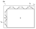
- FIG. 2 is a plan view of the thin film transistor substrate according to an embodiment of the present invention
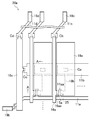
- 3 is an enlarged plan view of a pixel portion and a terminal portion of the thin film transistor substrate according to the embodiment of the present invention
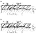
- FIG. 4 is a cross-sectional view of the thin film transistor substrate along the line AA in FIG. is there.
- the liquid crystal display device 50 includes a thin film transistor substrate 20a that is a display device substrate and a counter substrate 30 that is another display device substrate, and a thin film transistor substrate 20a and a counter substrate that are provided to face each other. 30 and a liquid crystal layer 40 which is a display medium layer provided between 30. Further, the liquid crystal display device 50 includes a sealing material 32 provided in a frame shape for adhering the thin film transistor substrate 20a and the counter substrate 30 to each other and enclosing the liquid crystal layer 40 between the thin film transistor substrate 20a and the counter substrate 30. I have.
- a display region D for displaying an image is defined in a portion inside the sealing material 32, and a terminal region T is formed in a portion protruding from the counter substrate 30 of the thin film transistor substrate 20a. It is prescribed.
- the thin film transistor substrate 20a includes an insulating substrate 10a, a plurality of scanning wirings 11a provided in the display region D so as to extend in parallel with each other on the insulating substrate 10a, A plurality of auxiliary capacitance lines 11b are provided between the scan lines 11a and extend in parallel to each other.
- the thin film transistor substrate 20a includes a plurality of signal wirings 16a provided so as to extend in parallel to each other in a direction orthogonal to each scanning wiring 11a, and each intersection of each scanning wiring 11a and each signal wiring 16a, that is, each pixel.
- Each includes a plurality of TFTs 5a provided for each, and an interlayer insulating film 17 provided so as to cover each TFT 5a.
- the thin film transistor substrate 20a is provided in a matrix on the interlayer insulating film 17, and a plurality of pixel electrodes 19a connected to the respective TFTs 5a and an alignment film (not shown) provided so as to cover the respective pixel electrodes 19a. And.
- the scanning wiring 11a is drawn out to the gate terminal region Tg of the terminal region T (see FIG. 1), and is connected to the gate terminal 19b in the gate terminal region Tg.
- the auxiliary capacity line 11b is connected to the auxiliary capacity terminal 19d via the auxiliary capacity main line 16c and the relay line 11d.
- the auxiliary capacity trunk line 16c is connected to the auxiliary capacity line 11b via the contact hole Cc formed in the gate insulating layer 12, and is connected to the relay line via the contact hole Cd formed in the gate insulating layer 12. 11d.
- the signal wiring 16a is led out as a relay wiring 11c to the source terminal region Ts in the terminal region T (see FIG. 1), and is connected to the source terminal 19c in the source terminal region Ts. Yes.
- the signal wiring 16a is connected to the relay wiring 11c through the contact hole Cb formed in the gate insulating layer 12, as shown in FIG.
- the TFT 5a has a bottom gate structure. As shown in FIGS. 3 and 4, the gate electrode 11aa provided on the insulating substrate 10a, and the gate insulating layer 12 provided so as to cover the gate electrode 11aa, And an oxide semiconductor layer 13a having a channel region C provided in an island shape so as to overlap with the gate electrode 11aa on the gate insulating layer 12.
- the TFT 5a includes a source electrode 16aa and a drain electrode 16b provided on the oxide semiconductor layer 13a so as to overlap the gate electrode 11aa and to face each other with the channel region C interposed therebetween.
- an interlayer insulating film 17 covering the source electrode 16aa and the drain electrode 16b (that is, the TFT 5a) is provided on the channel region C of the oxide semiconductor layer 13a.
- the gate electrode 11aa is a portion protruding to the side of the scanning wiring 11a.
- the source electrode 16aa is a portion protruding to the side of the signal wiring 16a.
- the source electrode 16aa is formed by a laminated film of the first conductive layer 14a and the second conductive layer 15a. It is configured.
- the drain electrode 16 b is configured by a laminated film of the first conductive layer 14 b and the second conductive layer 15 b, and is connected to the pixel via a contact hole Ca formed in the interlayer insulating film 17. It is connected to the electrode 19a. Further, the drain electrode 16b constitutes an auxiliary capacitance by overlapping with the auxiliary capacitance wiring 11b through the gate insulating layer 12.
- the oxide semiconductor layer 13a is formed of an oxide semiconductor film made of, for example, indium gallium zinc oxide (IGZO).
- IGZO indium gallium zinc oxide
- a channel protective layer (etching stopper layer) 25 for protecting the channel region C is provided in the channel region C of the oxide semiconductor layer 13a.
- the channel protective layer 25 By providing this channel protective layer 25, the channel region C of the oxide semiconductor layer 13a is not etched when the source electrode 16aa and the drain electrode 16b are formed by patterning by etching in a source / drain formation step described later. So that it can be protected.
- the counter substrate 30 includes an insulating substrate 10b, a black matrix 21 provided in a lattice shape on the insulating substrate 10b, and a red color provided between each lattice of the black matrix 21. And a color filter layer having a colored layer 22 such as a green layer and a blue layer.
- the counter substrate 30 includes a common electrode 23 provided so as to cover the color filter layer, a photo spacer 24 provided on the common electrode 23, and an alignment film (non-coated) provided so as to cover the common electrode 23. As shown).
- the liquid crystal layer 40 is made of, for example, a nematic liquid crystal material having electro-optical characteristics.
- the source driver ( A source signal is sent from the not-shown source signal 16a to the source electrode 16aa, and a predetermined charge is written to the pixel electrode 19a via the semiconductor layer 13a and the drain electrode 16b.
- a predetermined voltage is applied to the capacitor.
- liquid crystal display device 50 in each pixel, an image is displayed by adjusting the light transmittance of the liquid crystal layer 40 by changing the alignment state of the liquid crystal layer 40 according to the magnitude of the voltage applied to the liquid crystal layer 40. .
- the gate insulating layer 12 includes a first gate insulating layer 12a and a first gate insulating layer 12a provided on the insulating substrate 10a so as to cover the gate electrode 11aa.
- the second gate insulating layer 12b is provided on the oxide semiconductor layer 13a and is in contact with the oxide semiconductor layer 13a.
- the first gate insulating layer 12a is formed of a silicon nitride film (SiNx), and the second gate insulating layer 12b is formed of a silicon oxide film (SiOx).
- the second gate insulating layer 12b is formed by performing plasma treatment on the surface of the first gate insulating layer 12a made of silicon nitride.
- FIGS. 5 and 6 are explanatory views showing the manufacturing process of the TFT and the thin film transistor substrate in cross section
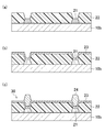
- FIG. 7 is an explanatory view showing the manufacturing process of the counter substrate in cross section.
- the manufacturing method of this embodiment includes a thin film transistor substrate manufacturing process, a counter substrate manufacturing process, and a liquid crystal injection process.
- a molybdenum film (thickness of about 150 nm) or the like is formed on the entire substrate of the insulating substrate 10a such as a glass substrate, a silicon substrate, or a heat-resistant plastic substrate by a sputtering method. Then, by performing photolithography, wet etching, and resist peeling and cleaning, as shown in FIGS. 3 and 5A, the scanning wiring 11a, the gate electrode 11aa, the auxiliary capacitance wiring 11b, and the relay wirings 11c and 11d are formed. Form.
- the molybdenum film having a single layer structure is exemplified as the metal film constituting the gate electrode 11aa.
- a metal such as an aluminum film, a tungsten film, a tantalum film, a chromium film, a titanium film, or a copper film is used.
- the gate electrode 11aa may be formed with a thickness of 50 nm to 500 nm using a film or a film made of such an alloy film or metal nitride.
- polyethylene terephthalate resin polyethylene naphthalate resin
- polyether sulfone resin acrylic resin
- polyimide resin polyimide resin
- a silicon nitride film (thickness of about 200 nm to 500 nm) is formed by plasma CVD on the entire substrate on which the scanning wiring 11a, the gate electrode 11aa, the auxiliary capacitance wiring 11b, and the relay wirings 11c and 11d are formed. Then, as shown in FIG. 5B, the first gate insulating layer 12a is formed so as to cover the gate electrode 11aa and the auxiliary capacitance line 11b.
- a second gate insulating layer 12b made of a silicon oxide film is formed on the first gate insulating layer 12a.
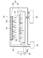
- FIG. 8 is a cross-sectional view showing the overall configuration of the plasma apparatus according to the embodiment of the present invention.
- the plasma apparatus 33 includes a plasma generation chamber (vacuum vessel) 34 and a plasma discharge generation unit 35 provided inside the plasma generation chamber 34. Then, the plasma apparatus 33 supplies part of the first gate insulating layer 12a to silicon oxide by supplying oxygen radicals to the surface of the first gate insulating layer 12a of the substrate to be processed 26 shown in FIG. 5B. Thus, the second gate insulating layer 12b made of a silicon oxide film is formed on the first gate insulating layer 12a.
- the plasma discharge generator 35 includes a pair of a cathode electrode (power electrode) 37 and an anode electrode (ground electrode) 36 that are disposed so as to face each other in the vertical direction in the plasma generation chamber 34. It has the electrode of.
- the anode electrode 36 and the cathode electrode 37 are installed in the plasma generation chamber 34 so as to be electrically insulated and parallel to each other.
- a high-frequency power source 42 that supplies power to the plasma discharge generation unit 35, and a gas supply unit 43 that supplies the source gas 41 into the plasma generation chamber 34
- a gas discharge unit 38 for discharging the gas in the plasma generation chamber 34 is provided.
- a gas supply pipe 39 for introducing the raw material gas 41 is formed between the anode electrode 36 and the cathode electrode 37.
- a plasma 27 is generated between the anode electrode 36 and the cathode electrode 37, and the generated plasma 27 generates a source gas (dinitrogen monoxide in the present embodiment) between the anode electrode 36 and the cathode electrode 37.
- a source gas dinitrogen monoxide in the present embodiment
- radicals oxygen radicals
- oxygen radicals are generated by decomposition of the raw material gas 41 by plasma.
- the oxygen radicals generated in this way are diffused to the surface of the first gate insulating layer 12a formed on the substrate to be processed 26, and a part of the first gate insulating layer 12a is changed to silicon oxide.
- a second gate insulating layer 12b made of a silicon oxide film is formed on the one gate insulating layer 12a.
- the source gas 41 is supplied from the gas supply unit 43 to the plasma generation chamber 34 while the substrate 26 is mounted on the anode electrode 36 and the inside of the plasma generation chamber 34 is depressurized by a vacuum pump or the like. Then, the high-frequency power source 42 is driven together with the introduction of the raw material gas 41 to apply a high-frequency voltage between the anode electrode 36 and the cathode electrode 37, thereby causing a raw material gas as a glow discharge phenomenon due to dielectric breakdown of the gas due to the generated electric field. 41 plasma states are produced.
- the oxygen radicals generated in this way diffuse to the substrate 26 to be processed and are supplied to the surface of the first gate insulating layer 12a formed on the substrate 26 to be processed, whereby the first gate insulating layer 12a.
- the second gate insulating layer 12b made of a silicon oxide film is formed on the first gate insulating layer 12a by replacing a part of the first gate insulating layer 12a with silicon oxide.
- the plasma apparatus 33 is also used when forming the first gate insulating layer 12a by forming a silicon nitride film by the above-described plasma CVD method. Therefore, since the second gate insulating layer 12b can be formed by changing the source gas supplied to the plasma device 33, it is not necessary to provide a separate device for forming the second gate insulating layer 12b. It becomes possible to suppress the cost increase.
- dinitrogen monoxide is used as a source gas
- surface treatment is performed by supplying oxygen radicals generated by atmospheric pressure plasma to the surface of the first gate insulating layer 12a, and then on the first gate insulating layer 12a.
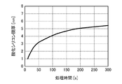
- the thickness of the formed silicon oxide film increases.
- a relatively short time It can be seen that the processing for 40 to 180 seconds may be performed. Note that when the processing time is short as described above, the number of substrates that can be processed per unit time can be increased, so that productivity can be improved and manufacturing cost can be suppressed.
- the thickness of the silicon oxide film (second gate insulating layer 12b) is preferably 3 to 5 nm. This is because when the thickness is less than 3 nm, the thickness of the silicon oxide film varies, and it may be difficult to effectively suppress the degradation of TFT characteristics. Further, when the thickness is larger than 5 nm, there is a possibility that the processing time becomes long.
- an interface stabilizing layer having a thickness of 50 to 5000 mm is formed by sputtering, but when the interface stabilizing layer is as thin as 50 to 100 mm, There is a problem that the film thickness of the interface stabilizing layer becomes non-uniform and it is difficult to satisfactorily suppress the deterioration of TFT characteristics.
- the productivity is improved without causing the disadvantage that the TFT characteristics are deteriorated due to the variation in the thickness of the silicon oxide film. It becomes possible.
- an oxide semiconductor film (thickness of about 30 nm to 100 nm) made of, for example, indium gallium zinc oxide is formed by sputtering, and then photolithography, wet etching, and resist are formed on the oxide semiconductor film. By performing peeling cleaning, an oxide semiconductor layer 13a is formed over the second gate insulating layer 12b as illustrated in FIG.
- the oxide semiconductor layer 12b is different from the case where an oxide semiconductor layer is provided over the gate insulating layer made of a silicon nitride film. It becomes possible to prevent the formation of impurity levels and fixed charges at the interface between the layer and the silicon oxide film. Accordingly, it is possible to suppress the deterioration of the characteristics of the TFT 5a by suppressing the fluctuation of the threshold voltage of the TFT 5a.
- a silicon nitride film, a silicon oxide film, a silicon nitride oxide film, or the like is formed over the entire substrate over which the oxide semiconductor layer 13a is formed by a plasma CVD method. Thereafter, by performing photolithography, etching, and resist peeling cleaning using the resist as a mask, a channel for protecting the channel region C in the channel region C of the oxide semiconductor layer 13a as shown in FIG.
- a protective layer (etching stopper layer) 25 is formed to a thickness of about 50 to 100 nm.
- a titanium film (thickness: 30 nm to 150 nm) and a copper film (thickness: about 50 nm to 400 nm) are sequentially formed on the entire substrate on which the oxide semiconductor layer 13a is formed by a sputtering method. Thereafter, photolithography and wet etching are performed on the copper film, and dry etching and resist peeling cleaning are performed on the titanium film, so that the signal wiring 16a (see FIG. 5F) is obtained. 3), the source electrode 16aa, the drain electrode 16b, and the auxiliary capacity trunk line 16c (see FIG. 3) are formed, and the channel region C of the semiconductor layer 13a is exposed.
- the source electrode 16aa and the drain electrode 16b are formed by dry etching on the oxide semiconductor layer 13a formed in the semiconductor layer forming step, and the channel region C of the oxide semiconductor layer 13a is exposed.
- the metal film constituting the source electrode 16aa and the drain electrode 16b a titanium film and a copper film having a laminated structure are exemplified.
- a metal such as an aluminum film, a tungsten film, a tantalum film, or a chromium film is used.
- the source electrode 16aa and the drain electrode 16b may be formed by a film, or a film of an alloy film or metal nitride thereof.
- etching process either dry etching or wet etching described above may be used. However, when processing a large area substrate, it is preferable to use dry etching.
- a fluorine-based gas such as CF 4 , NF 3 , SF 6 , or CHF 3
- a chlorine-based gas such as Cl 2 , BCl 3 , SiCl 4 , or CCl 4
- an oxygen-based gas or the like
- An inert gas such as helium or argon may be added.
- a silicon oxide film is formed by plasma CVD on the entire substrate on which the source electrode 16aa and the drain electrode 16b are formed (that is, the TFT 5a is formed), as shown in FIG.
- an interlayer insulating film 17 covering the TFT 5a is formed to a thickness of about 400 nm.
- a transparent conductive film such as an ITO film (thickness of about 50 nm to 200 nm) made of indium tin oxide, for example, is formed on the entire substrate on which the interlayer insulating film 17 is formed by sputtering.
- the pixel electrode 19a, the gate terminal 19b, the source terminal 19c, and the auxiliary capacitance terminal 19d are formed as shown in FIG. Form.
- the pixel electrode 19a is formed on the surface of the interlayer insulating film 17 so as to cover the surface of the contact hole Ca.
- the pixel electrode 19a is made of indium oxide containing tungsten oxide, indium zinc oxide, indium oxide containing titanium oxide, indium tin oxide, or the like. Can do. In addition to indium tin oxide (ITO), indium zinc oxide (IZO), indium tin oxide containing silicon oxide (ITSO), and the like can also be used.
- ITO indium tin oxide
- IZO indium zinc oxide
- ITSO indium tin oxide containing silicon oxide
- the conductive thin film is made of titanium, tungsten, nickel, gold, platinum, silver, aluminum, magnesium, calcium, lithium, or an alloy thereof. A film can be used, and this metal thin film can be used as the pixel electrode 19a.
- the thin film transistor substrate 20a shown in FIG. 4 can be manufactured.
- ⁇ Opposite substrate manufacturing process First, by applying a photosensitive resin colored in black, for example, by spin coating or slit coating to the entire substrate of the insulating substrate 10b such as a glass substrate, the coating film is exposed and developed to obtain a figure. As shown in FIG. 7A, the black matrix 21 is formed to a thickness of about 1.0 ⁇ m.
- a photosensitive resin colored in red, green, or blue is applied to the entire substrate on which the black matrix 21 is formed by spin coating or slit coating. Thereafter, the coating film is exposed and developed to form a colored layer 22 (for example, a red layer) of a selected color with a thickness of about 2.0 ⁇ m as shown in FIG. The same process is repeated for the other two colors to form the other two colored layers 22 (for example, a green layer and a blue layer) with a thickness of about 2.0 ⁇ m.
- the common electrode 23 has a thickness as shown in FIG. It is formed to have a thickness of about 50 nm to 200 nm.
- the photo spacer 24 is formed to a thickness of about 4 ⁇ m.
- the counter substrate 30 can be manufactured as described above.
- ⁇ Liquid crystal injection process> First, after applying a polyimide resin film to each surface of the thin film transistor substrate 20a produced in the thin film transistor substrate production process and the counter substrate 30 produced in the counter substrate production process by a printing method, Then, an alignment film is formed by performing baking and rubbing treatment.
- a sealing material made of UV (ultraviolet) curing and thermosetting resin is printed on the surface of the counter substrate 30 on which the alignment film is formed in a frame shape, a liquid crystal material is placed inside the sealing material. Dripping.
- the bonded body is released to atmospheric pressure, The front and back surfaces of the bonded body are pressurized.
- the unnecessary part is removed by dividing the bonding body which hardened the above-mentioned sealing material, for example by dicing.
- the liquid crystal display device 50 of the present embodiment can be manufactured.
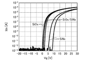
- FIG. 10 is an Ids-Vg characteristic diagram showing the relationship between the drain-source current (Ids) and the gate voltage (Vg) in the thin film transistor according to the embodiment of the present invention.
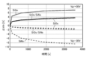
- FIG. 11 is a diagram showing a stress evaluation test result of the thin film transistor according to the embodiment of the present invention.
- measurement was performed by changing the gate voltage (Vg) in the range of ⁇ 20 to 30 V and setting the potential difference (Vds) between the drain and the source to 10 V. Further, in FIG. 11, measurement was performed by changing the gate voltage (Vg) to + 30V or ⁇ 30V with the substrate temperature set to 60 ° C. and the source voltage and drain voltage set to 0V.
- the S value (the value of Vg at which the drain current increases by an order of magnitude in the Vg ⁇ Vth region and calculated by ⁇ Vg / ⁇ log (Id) [unit: V / decade]) is small, It can also be seen that the hysteresis is small. Therefore, it can be seen that the characteristics of the TFT 5a are improved by using the gate insulating layer 12 of the present invention.
- the gate insulating layer 12 composed of the first gate insulating layer 12a formed of the silicon nitride film and the second gate insulating layer 12b formed of the silicon oxide film is used. Similar to the case of using a gate insulating layer formed of a silicon oxide film, the amount of change in threshold voltage ( ⁇ Vth) is small compared to the case of using a gate insulating layer formed of a silicon nitride film, and the reliability of the TFT 5a is improved. It turns out that the property becomes good.
- oxygen radicals are supplied to the surface of the first gate insulating layer 12a to A gate insulating layer constituted by the first gate insulating layer 12a and the second gate insulating layer 12b is formed by forming a second gate insulating layer 12b made of a silicon oxide film on the first gate insulating layer 12a. 12 is formed. In addition, the oxide semiconductor layer 13a is formed over the second gate insulating layer 12b.
- oxygen radicals generated by the plasma treatment are supplied. Therefore, since oxygen radicals are generated by plasma treatment, oxygen radicals can be generated by a simple method.
- oxygen radicals are generated by decomposition of dinitrogen monoxide gas with plasma. Accordingly, oxygen radicals can be generated by a simple method.
- the channel protective layer 25 that protects the channel region C is formed in the channel region C of the oxide semiconductor layer 13a. Therefore, in the step of forming the source electrode 16aa and the drain electrode 16b, patterning is performed by etching to protect the channel region C of the oxide semiconductor layer 13a from being etched when the source electrode 16aa and the drain electrode 16b are formed. It becomes possible to do.
- the oxide semiconductor layer is formed of an oxide semiconductor film made of indium gallium zinc oxide (IGZO). Accordingly, good characteristics such as high mobility and low off-state current can be obtained in the TFT 5a.
- IGZO indium gallium zinc oxide
- dinitrogen monoxide is used as the plasma source gas, but oxygen gas may be used instead of dinitrogen monoxide.
- a plasma state of the oxygen gas which is the source gas, is generated, which promotes dissociation of the oxygen gas and causes high-density radicals (oxygen radicals) to enter the source gas. Generated. Then, by supplying a source gas containing oxygen radicals to the surface of the first gate insulating layer 12a formed on the substrate to be processed 26, a part of the first gate insulating layer 12a is changed to silicon oxide, and the first gate is changed. A second gate insulating layer 12b made of a silicon oxide film can be formed on the insulating layer 12a.
- oxygen radicals can be generated by a simple method.
- the channel protective layer 25 is provided.
- the thin film transistor substrate 20a may adopt a channel etch structure in which the channel protective layer 25 is not provided.
- an oxide semiconductor film made of indium gallium zinc oxide (IGZO) or the like is used as the oxide semiconductor layer 13a.
- the oxide semiconductor layer 13a is not limited to this, and indium (In)
- a material made of a metal oxide containing at least one of gallium (Ga), aluminum (Al), copper (Cu), zinc (Zn), magnesium (Mg), and cadmium (Cd) may be used. Since the oxide semiconductor layer 13a formed using any of these materials has high mobility even when it is amorphous, the on-resistance of the switching element can be reduced. Therefore, the difference in output voltage at the time of data reading becomes large, and the S / N ratio can be improved.
- oxide semiconductor films such as InGaO 3 (ZnO) 5 , Mg x Zn 1-x O, Cd x Zn 1-x O, and CdO can be given. it can.
- an amorphous state, a polycrystalline state, or a non-crystalline state of ZnO to which one or more kinds of impurity elements of Group 1 element, Group 13 element, Group 14 element, Group 15 element, or Group 17 element are added is also possible to use a microcrystalline state in which a crystalline state and a polycrystalline state are mixed, or a material to which the above impurities are not added.
- the display device can be an organic EL (organic electro luminescence), electrophoresis (electrophoretic), PD (plasma display), PALC. (Plasma addressed liquid crystal display), inorganic EL (inorganic electroluminescence), FED (field emission display), SED (surface-conduction electron-emitter display), etc. It may be a display device.
- Examples of utilization of the present invention include a method for manufacturing a thin film transistor substrate using a semiconductor layer of an oxide semiconductor, a thin film transistor substrate manufactured by the method, and a display device.
Landscapes
- Thin Film Transistor (AREA)
- Liquid Crystal (AREA)
- Electroluminescent Light Sources (AREA)
Abstract
薄膜トランジスタ基板の製造方法あって、絶縁基板(10a)上にゲート電極(11aa)を形成する工程と、ゲート電極(11a)を覆うように窒化シリコン膜からなる第1ゲート絶縁層(12a)を形成した後、第1ゲート絶縁層(12a)の表面に対して酸素ラジカルを供給して表面処理を行い、第1ゲート絶縁層(12a)上に酸化シリコン膜からなる第2ゲート絶縁層(12b)を形成する工程と、第2ゲート絶縁層(12b)上に酸化物半導体層(12a)を形成する工程とを備える。
Description
本発明は、薄膜トランジスタに関し、特に、酸化物半導体の半導体層を用いた薄膜トランジスタ基板の製造方法およびその方法により製造された薄膜トランジスタ基板、表示装置に関する。
アクティブマトリクス基板では、画像の最小単位である各画素毎に、スイッチング素子として、例えば、薄膜トランジスタ(Thin Film Transistor、以下、「TFT」とも称する)が設けられている。
一般的なボトムゲート型のTFTは、例えば、絶縁基板上に設けられたゲート電極と、ゲート電極を覆うように設けられたゲート絶縁層と、ゲート絶縁層上にゲート電極に重なるように島状に設けられた半導体層と、半導体層上に互いに対峙するように設けられたソース電極及びドレイン電極とを備えている。
また、近年、アクティブマトリクス基板では、画像の最小単位である各画素のスイッチング素子として、アモルファスシリコンの半導体層を用いた従来の薄膜トランジスタに代わって、移動度に優れた酸化物半導体の半導体層(以下、「酸化物半導体層」とも称する。)を用いたTFTが提案されている。
この酸化物半導体層を用いたTFTでは、一般に、ゲート絶縁層として、CVD法で成膜される窒化シリコン膜が使用されている。しかし、ゲート絶縁層に窒化シリコン膜を使用すると、ゲート絶縁層上に設けられた酸化物半導体層と窒化シリコン膜との界面に、不純物準位や固定電荷が形成されやすいため、TFTの閾値電圧に変動が生じ、結果として、TFT特性が低下するという問題があった。
そこで、酸化物半導体層とゲート絶縁層との界面特性を向上させるための薄膜トランジスタ基板が提案されている。より具体的には、酸化物半導体層とゲート絶縁層との間に、3.0~8.0eVのバンドギャップを有する酸化物からなる界面安定化層を設けた薄膜トランジスタ基板が開示されている。そして、このような界面安定化層を設けることにより、酸化物半導体層の界面特性を向上することができると記載されている(例えば、特許文献1参照)。
しかし、上記特許文献1に記載の薄膜トランジスタ基板では、界面安定化層を形成するための成膜装置が別個に必要となるため、コストアップになるという問題があった。
また、酸化物半導体層を使用する場合、窒化シリコン膜の代わりに、酸化物半導体層との界面において、窒化シリコン膜に比し不純物準位や固定電荷といった電荷トラップが形成され難いと考えられる酸化シリコン膜を使用することも考えられる。
しかし、アモルファスシリコンを用いた従来の薄膜トランジスタ基板の製造工程においては、酸化シリコン膜を成膜するための成膜装置が設けられていないため、酸化物半導体層を用いた薄膜トランジスタ基板を製造する際に、酸化シリコン膜を形成するための別個の成膜装置を設ける必要があり、コストアップになるという問題があった。
そこで、本発明は上述の問題に鑑みてなされたものであり、酸化物半導体層を用いた薄膜トランジスタ基板において、閾値電圧の変動を抑制して、TFT特性の低下を効果的に抑制することができるとともに、コストアップを抑制することができる薄膜トランジスタ基板の製造方法およびその方法により製造された薄膜トランジスタ基板、表示装置を提供することを目的とする。
上記目的を達成するために、本発明の薄膜トランジスタ基板の製造方法は、絶縁基板と、絶縁基板に設けられたゲート電極と、ゲート電極を覆うように設けられたゲート絶縁層と、ゲート絶縁層上に設けられ、ゲート電極に重なるように設けられたチャネル領域を有する酸化物半導体層とを備えた薄膜トランジスタ基板の製造方法あって、絶縁基板上にゲート電極を形成するゲート電極形成工程と、ゲート電極を覆うように窒化シリコン膜からなる第1ゲート絶縁層を形成した後、第1ゲート絶縁層の表面に対して酸素ラジカルを供給して表面処理を行い、第1ゲート絶縁層上に酸化シリコン膜からなる第2ゲート絶縁層を形成することにより、第1ゲート絶縁層と第2ゲート絶縁層とにより構成されたゲート絶縁層を形成するゲート絶縁層形成工程と、第2ゲート絶縁層上に酸化物半導体層を形成する半導体層形成工程とを少なくとも備えることを特徴とする。
同構成によれば、酸化物半導体層と酸化シリコン膜からなる第2ゲート絶縁層との界面における不純物準位や固定電荷の形成を防止することが可能になる。その結果、薄膜トランジスタの閾値電圧の変動を抑制して、薄膜トランジスタの特性の低下を効果的に抑制することが可能になる。
また、例えば、プラズマ装置により、第1ゲート絶縁層を形成する場合、第1ゲート絶縁層を形成する際に使用するプラズマ装置に供給する原料ガスを変更することにより、第2ゲート絶縁層を形成することができるため、酸化シリコン膜からなる第2ゲート絶縁層を形成するために、別個の成膜装置を設ける必要がなく、コストアップを抑制することが可能になる。
本発明の薄膜トランジスタ基板の製造方法においては、表面処理は、プラズマ処理により発生した酸素ラジカルを供給する処理であってもよい。
同構成によれば、プラズマ処理により酸素ラジカルを発生させるため、簡単な方法で酸素ラジカルを発生させることできる。
本発明の薄膜トランジスタ基板の製造方法においては、酸素ラジカルは、一酸化二窒素ガスのプラズマによる分解により発生させたものであってもよい。
同構成によれば、簡単な方法で、酸素ラジカルを発生させることが可能になる。
本発明の薄膜トランジスタ基板の製造方法においては、酸素ラジカルは、酸素ガスのプラズマによる分解により発生させたものであってもよい。
同構成によれば、簡単な方法で、酸素ラジカルを発生させることが可能になる。
本発明の薄膜トランジスタ基板の製造方法においては、半導体層形成工程後、酸化物半導体層のチャネル領域にチャネル領域を保護するチャネル保護層を形成するチャネル保護層形成工程を更に備えてもよい。
同構成によれば、酸化物半導体層上にソース電極及びドレイン電極を形成する工程において、エッチングによりパターンニングして、ソース電極、ドレイン電極を形成する際に、酸化物半導体層のチャネル領域をエッチングしないように保護することが可能になる。
本発明の薄膜トランジスタ基板の製造方法においては、酸化物半導体層が、インジウム(In)、ガリウム(Ga)、アルミニウム(Al)、銅(Cu)、亜鉛(Zn)、マグネシウム(Mg)、及びカドミウム(Cd)からなる群より選ばれる少なくとも1種を含む金属酸化物からなってもよい。
同構成によれば、これらの材料からなる酸化物半導体層は、アモルファスであっても移動度が高いため、スイッチング素子のオン抵抗を小さくすることができる。
本発明の薄膜トランジスタ基板の製造方法においては、酸化物半導体層が、酸化インジウムガリウム亜鉛(IGZO)からなる酸化物半導体膜により形成されていてもよい。
同構成によれば、薄膜トランジスタにおいて、高移動度、低オフ電流という良好な特性を得ることができる。
本発明の薄膜トランジスタ基板は、本発明の薄膜トランジスタ基板の製造方法により製造されたものである。
同構成によれば、本発明の薄膜トランジスタ基板の製造方法と同じ効果を有する薄膜トランジスタ基板を得ることが可能になる。
また、本発明の薄膜トランジスタ基板は、薄膜トランジスタの閾値電圧の変動を抑制して、薄膜トランジスタの特性の低下を効果的に抑制することができ、コストアップを抑制することができるという優れた特性を備えている。従って、本発明の薄膜トランジスタ基板は、薄膜トランジスタ基板と、薄膜トランジスタ基板に対向して配置された対向基板と、薄膜トランジスタ基板及び対向基板の間に設けられた表示媒体層とを備える表示装置に好適に使用できる。また、本発明の表示装置は、表示媒体層が液晶層である表示装置に好適に使用できる。
本発明によれば、酸化物半導体層を用いた薄膜トランジスタ基板において、閾値電圧の変動を抑制して、TFT特性の低下を効果的に抑制することができるとともに、コストアップを抑制することができる。
(第1の実施形態)
以下、本発明の実施形態について、図面を参照しながら詳細に説明する。尚、本発明は以下の実施形態に限定されるものではない。
以下、本発明の実施形態について、図面を参照しながら詳細に説明する。尚、本発明は以下の実施形態に限定されるものではない。
図1は、本発明の実施形態に係る薄膜トランジスタ基板を有する液晶表示装置の断面図であり、図2は、本発明の実施形態に係る薄膜トランジスタ基板の平面図である。また、図3は、本発明の実施形態に係る薄膜トランジスタ基板の画素部及び端子部を拡大した平面図であり、図4は、図3中のA-A線に沿った薄膜トランジスタ基板の断面図である。
液晶表示装置50は、図1に示すように、互いに対向するように設けられた表示装置用基板である薄膜トランジスタ基板20a及び他の表示装置用基板である対向基板30と、薄膜トランジスタ基板20a及び対向基板30の間に設けられた表示媒体層である液晶層40とを備えている。また、液晶表示装置50は、薄膜トランジスタ基板20a及び対向基板30を互いに接着するとともに、薄膜トランジスタ基板20a及び対向基板30の間に液晶層40を封入するために枠状に設けられたシール材32とを備えている。
また、液晶表示装置50では、図1に示すように、シール材32の内側の部分に画像表示を行う表示領域Dが規定され、薄膜トランジスタ基板20aの対向基板30から突出する部分に端子領域Tが規定されている。
薄膜トランジスタ基板20aは、図2、図3及び図4に示すように、絶縁基板10aと、表示領域Dにおいて、絶縁基板10a上に互いに平行に延びるように設けられた複数の走査配線11aと、各走査配線11aの間にそれぞれ設けられ、互いに平行に延びる複数の補助容量配線11bとを備えている。また、薄膜トランジスタ基板20aは、各走査配線11aと直交する方向に互いに平行に延びるように設けられた複数の信号配線16aと、各走査配線11a及び各信号配線16aの交差部分毎、すなわち、各画素毎にそれぞれ設けられた複数のTFT5aと、各TFT5aを覆うように設けられた層間絶縁膜17とを備えている。また、薄膜トランジスタ基板20aは、層間絶縁膜17上にマトリクス状に設けられ、各TFT5aにそれぞれ接続された複数の画素電極19aと、各画素電極19aを覆うように設けられた配向膜(不図示)とを備えている。
走査配線11aは、図2及び図3に示すように、端子領域T(図1参照)のゲート端子領域Tgに引き出され、そのゲート端子領域Tgにおいて、ゲート端子19bに接続されている。
補助容量配線11bは、図3に示すように、補助容量幹線16c及び中継配線11dを介して補助容量端子19dに接続されている。ここで、補助容量幹線16cは、ゲート絶縁層12に形成されたコンタクトホールCcを介して補助容量配線11bに接続されているとともに、ゲート絶縁層12に形成されたコンタクトホールCdを介して中継配線11dに接続されている。
信号配線16aは、図2及び図3に示すように、端子領域T(図1参照)のソース端子領域Tsに中継配線11cとして引き出され、そのソース端子領域Tsにおいて、ソース端子19cに接続されている。
ここで、信号配線16aは、図3に示すように、ゲート絶縁層12に形成されたコンタクトホールCbを介して中継配線11cに接続されている。
TFT5aは、ボトムゲート構造を有しており、図3及び図4に示すように、絶縁基板10a上に設けられたゲート電極11aaと、ゲート電極11aaを覆うように設けられたゲート絶縁層12と、ゲート絶縁層12上でゲート電極11aaに重なるように島状に設けられたチャネル領域Cを有する酸化物半導体層13aとを備えている。また、TFT5aは、酸化物半導体層13a上にゲート電極11aaに重なるとともにチャネル領域Cを挟んで互いに対峙するように設けられたソース電極16aa及びドレイン電極16bとを備えている。
ここで、酸化物半導体層13aのチャネル領域C上には、ソース電極16aa及びドレイン電極16b(即ち、TFT5a)を覆う層間絶縁膜17が設けられている。
また、ゲート電極11aaは、図3に示すように、走査配線11aの側方への突出した部分である。また、ソース電極16aaは、図3に示すように、信号配線16aの側方への突出した部分であり、図4に示すように、第1導電層14a及び第2導電層15aの積層膜により構成されている。
さらに、ドレイン電極16bは、図3及び図4に示すように、第1導電層14b及び第2導電層15bの積層膜により構成され、層間絶縁膜17に形成されたコンタクトホールCaを介して画素電極19aに接続されている。また、ドレイン電極16bは、ゲート絶縁層12を介して補助容量配線11bと重なることにより補助容量を構成している。
また、酸化物半導体層13aは、例えば、酸化インジウムガリウム亜鉛(IGZO)等からなる酸化物半導体膜により形成されている。
また、本実施形態においては、図4に示すように、酸化物半導体層13aのチャネル領域Cに、当該チャネル領域Cを保護するためのチャネル保護層(エッチングストッパ層)25が設けられている。このチャネル保護層25を設けることにより、後述するソースドレイン形成工程において、エッチングによりパターンニングして、ソース電極16aa、ドレイン電極16bを形成する際に、酸化物半導体層13aのチャネル領域Cをエッチングしないように保護することが可能になる。
対向基板30は、後述する図7(c)に示すように、絶縁基板10bと、絶縁基板10b上に格子状に設けられたブラックマトリクス21並びにブラックマトリクス21の各格子間にそれぞれ設けられた赤色層、緑色層及び青色層などの着色層22を有するカラーフィルター層とを備えている。また、対向基板30は、そのカラーフィルター層を覆うように設けられた共通電極23と、共通電極23上に設けられたフォトスペーサ24と、共通電極23を覆うように設けられた配向膜(不図示)とを備えている。
液晶層40は、例えば、電気光学特性を有するネマチックの液晶材料などにより構成されている。
上記構成の液晶表示装置50では、各画素において、ゲートドライバ(不図示)からゲート信号が走査配線11aを介してゲート電極11aaに送られて、TFT5aがオン状態になったときに、ソースドライバ(不図示)からソース信号が信号配線16aを介してソース電極16aaに送られて、半導体層13a及びドレイン電極16bを介して、画素電極19aに所定の電荷が書き込まれる。
この際、薄膜トランジスタ基板20aの各画素電極19aと対向基板30の共通電極23との間において電位差が生じ、液晶層40、すなわち、各画素の液晶容量、及びその液晶容量に並列に接続された補助容量に所定の電圧が印加される。
そして、液晶表示装置50では、各画素において、液晶層40に印加する電圧の大きさによって液晶層40の配向状態を変えることにより、液晶層40の光透過率を調整して画像が表示される。
また、本実施形態においては、図4に示すように、ゲート絶縁層12は、絶縁基板10a上にゲート電極11aaを覆うように設けられた第1ゲート絶縁層12aと、第1ゲート絶縁層12a上に設けられ、酸化物半導体層13aと接する第2ゲート絶縁層12bとにより構成されている。
第1ゲート絶縁層12aは、窒化シリコン膜(SiNx)により形成されており、第2ゲート絶縁層12bは、酸化シリコン膜(SiOx)により形成されている。そして、本実施形態においては、第2ゲート絶縁層12bは、窒化シリコンからなる第1ゲート絶縁層12aの表面に対してプラズマ処理を施すことにより形成される構成となっている。
次に、本実施形態の液晶表示装置50の製造方法の一例について、図5~図7を用いて説明する。図5、図6は、TFT及び薄膜トランジスタ基板の製造工程を断面で示す説明図であり、図7は、対向基板の製造工程を断面で示す説明図である。なお、本実施形態の製造方法は、薄膜トランジスタ基板作製工程、対向基板作製工程及び液晶注入工程を備える。
まず、TFT及び薄膜トランジスタ基板作製工程について説明する。
<ゲート電極形成工程>
まず、ガラス基板、シリコン基板、耐熱性を有するプラスチック基板などの絶縁基板10aの基板全体に、スパッタリング法により、例えば、モリブテン膜(厚さ150nm程度)などを成膜した後に、そのモリブテン膜に対して、フォトリソグラフィ、ウエットエッチング及びレジストの剥離洗浄を行うことにより、図3、図5(a)に示すように、走査配線11a、ゲート電極11aa、補助容量配線11b、並びに中継配線11c,11dを形成する。
まず、ガラス基板、シリコン基板、耐熱性を有するプラスチック基板などの絶縁基板10aの基板全体に、スパッタリング法により、例えば、モリブテン膜(厚さ150nm程度)などを成膜した後に、そのモリブテン膜に対して、フォトリソグラフィ、ウエットエッチング及びレジストの剥離洗浄を行うことにより、図3、図5(a)に示すように、走査配線11a、ゲート電極11aa、補助容量配線11b、並びに中継配線11c,11dを形成する。
なお、本実施形態では、ゲート電極11aaを構成する金属膜として、単層構造のモリブテン膜を例示したが、例えば、アルミニウム膜、タングステン膜、タンタル膜、クロム膜、チタン膜、銅膜等の金属膜、または、これらの合金膜や金属窒化物による膜によりゲート電極11aaを、50nm~500nmの厚さで形成する構成としても良い。
また、上記プラスチック基板を形成する材料としては、例えば、ポリエチレンテレフタレート樹脂、ポリエチレンナフタレート樹脂、ポリエーテルサルフォン樹脂、アクリル樹脂、及びポリイミド樹脂を使用することができる。
<ゲート絶縁層形成工程>
まず、走査配線11a、ゲート電極11aa、補助容量配線11b、並びに中継配線11c,11dが形成された基板全体に、プラズマCVD法により、例えば、窒化シリコン膜(厚さ200nm~500nm程度)を成膜して、図5(b)に示すように、ゲート電極11aa、及び補助容量配線11bを覆うように第1ゲート絶縁層12aを形成する。
まず、走査配線11a、ゲート電極11aa、補助容量配線11b、並びに中継配線11c,11dが形成された基板全体に、プラズマCVD法により、例えば、窒化シリコン膜(厚さ200nm~500nm程度)を成膜して、図5(b)に示すように、ゲート電極11aa、及び補助容量配線11bを覆うように第1ゲート絶縁層12aを形成する。
次いで、窒化シリコンからなる第1ゲート絶縁層12aの表面に対してプラズマ処理により発生した酸素ラジカル(O2
-)を供給して表面処理を行うことにより、図5(c)に示すように、第1ゲート絶縁層12a上に酸化シリコン膜からなる第2ゲート絶縁層12bを形成する。
図8は、本発明の実施形態に係るプラズマ装置の全体構成を示す断面図である。
プラズマ装置33は、図8に示すように、プラズマ発生室(真空容器)34と、プラズマ発生室34の内部に設けられたプラズマ放電発生部35とを備えている。そして、プラズマ装置33は、図5(b)に示す被処理基板26の第1ゲート絶縁層12aの表面に酸素ラジカルを供給することにより、第1ゲート絶縁層12aの一部を酸化シリコンに変えて、第1ゲート絶縁層12a上に酸化シリコン膜からなる第2ゲート絶縁層12bを形成するように構成されている。
プラズマ放電発生部35は、図8に示すように、プラズマ発生室34内で上下方向に互いに対向するように配置されたカソード電極(電源電極)37とアノード電極(接地電極)36とからなる一対の電極を有している。なお、アノード電極36とカソード電極37は、プラズマ発生室34において、電気的に絶縁され、互いに平行となるように設置されている。
また、プラズマ発生室34の外部には、図8に示すように、プラズマ放電発生部35に電力を供給する高周波電源42と、原料ガス41をプラズマ発生室34内に供給するガス供給部43と、プラズマ発生室34内のガスを排出するガス排出部38とが設けられている。また、プラズマ発生室34には、アノード電極36とカソード電極37との間に、原料ガス41を導入するためのガス供給管39が形成されている。
そして、アノード電極36とカソード電極37との間にプラズマ27を発生させ、発生したプラズマ27により、アノード電極36とカソード電極37との間において、原料ガス(本実施形態においては、一酸化二窒素ガス)41の解離が促進されることにより、ラジカル(酸素ラジカル)が生成される。
即ち、本実施形態においては、原料ガス41のプラズマによる分解により酸素ラジカルを発生させる構成としている。
そして、このように生成された酸素ラジカルを被処理基板26に形成された第1ゲート絶縁層12aの表面にまで拡散させて、第1ゲート絶縁層12aの一部を酸化シリコンに変えて、第1ゲート絶縁層12a上に酸化シリコン膜からなる第2ゲート絶縁層12bを形成するように構成されている。
より具体的には、アノード電極36上に被処理基板26を装着して真空ポンプ等でプラズマ発生室34の内部を減圧にした状態で、ガス供給部43から原料ガス41をプラズマ発生室34に導入し、原料ガス41の導入とともに高周波電源42を駆動させてアノード電極36とカソード電極37との間に高周波電圧を印加することにより、発生した電界による気体の絶縁破壊によってグロー放電現象として原料ガス41のプラズマ状態を生じさせる。これにより、カソード電極37の近傍において比較的強い電界が形成されるカソードシース部や、その付近において、原料ガス41の解離が促進されて酸素ラジカルが生成される。そして、このように生成された酸素ラジカルが、被処理基板26にまで拡散し、被処理基板26に形成された第1ゲート絶縁層12aの表面に供給されることにより、第1ゲート絶縁層12aの一部を酸化シリコンに変えて、第1ゲート絶縁層12a上に酸化シリコン膜からなる第2ゲート絶縁層12bを形成するように構成されている。
なお、本実施形態においては、このプラズマ装置33は、上述のプラズマCVD法により窒化シリコン膜を成膜して、第1ゲート絶縁層12aを形成する際にも使用されるものである。従って、プラズマ装置33に供給する原料ガスを変更することにより、第2ゲート絶縁層12bを形成することができるため、第2ゲート絶縁層12bを形成するために、別個の装置を設ける必要がなく、コストアップを抑制することが可能になる。
図9は、一酸化二窒素を原料ガスとして使用し、第1ゲート絶縁層12aの表面に対して常圧プラズマにより発生した酸素ラジカルを供給して表面処理を行い、第1ゲート絶縁層12a上に酸化シリコン膜からなる第2ゲート絶縁層12bを形成した場合の処理時間と酸化シリコン膜の膜厚との関係を示す図である。
図9に示すように、処理時間が長くなるにつれて、形成される酸化シリコン膜の膜厚も大きくなるが、3~5nmの厚みを有する酸化シリコン膜を形成するためには、比較的短時間(40~180秒)の処理を行えば良いことが判る。なお、このように処理時間が短い場合、単位時間当たりに処理できる基板の数を増加させることができるため、生産性が向上するとともに、製造コストを抑制することができる。
また、本実施形態においては、酸化シリコン膜(第2ゲート絶縁層12b)の厚みが3~5nmであることが好ましい。これは、厚みが3nm未満の場合は、酸化シリコン膜の膜厚にバラツキが生じ、TFT特性の低下を効果的に抑制することが困難になるという不都合が生じる場合があるためである。また、厚みが5nmよりも大きい場合は、処理時間が長くなるという不都合が生じる場合があるためである。
即ち、上記従来技術の薄膜トランジスタ基板においては、スパッタリング法により、50~5000Åの厚みを有する界面安定化層を成膜する構成であるが、界面安定化層の厚みが50~100Åと薄い場合は、界面安定化層の膜厚が不均一になり、TFT特性の低下を良好に抑制することが困難になるという問題があった。
一方、本実施形態においては、酸化シリコン膜の厚みを3~5nmに設定することにより、酸化シリコン膜の膜厚のバラツキに起因するTFT特性の低下という不都合を生じることなく、生産性を向上させることが可能になる。
<半導体層形成工程>
その後、スパッタリング法により、例えば、酸化インジウムガリウム亜鉛からなる酸化物半導体膜(厚さ30nm~100nm程度)を成膜し、その後、その酸化物半導体膜に対して、フォトリソグラフィ、ウエットエッチング及びレジストの剥離洗浄を行うことにより、図5(d)に示すように、第2ゲート絶縁層12b上に酸化物半導体層13aを形成する。
その後、スパッタリング法により、例えば、酸化インジウムガリウム亜鉛からなる酸化物半導体膜(厚さ30nm~100nm程度)を成膜し、その後、その酸化物半導体膜に対して、フォトリソグラフィ、ウエットエッチング及びレジストの剥離洗浄を行うことにより、図5(d)に示すように、第2ゲート絶縁層12b上に酸化物半導体層13aを形成する。
この際、本実施形態においては、第2ゲート絶縁層12bが、酸化シリコン膜により形成されているため、窒化シリコン膜からなるゲート絶縁層上に酸化物半導体層を設ける場合と異なり、酸化物半導体層と酸化シリコン膜との界面における不純物準位や固定電荷の形成を防止することが可能になる。従って、TFT5aの閾値電圧の変動を抑制して、TFT5aの特性の低下を効果的に抑制することが可能になる。
<チャネル保護層形成工程>
次いで、酸化物半導体層13aが形成された基板全体に、プラズマCVD法により、例えば、窒化シリコン膜、酸化シリコン膜、窒化酸化シリコン膜などを成膜する。その後、レジストをマスクとしてフォトリソグラフィ、エッチング及びレジストの剥離洗浄を行うことにより、図5(e)に示すように、酸化物半導体層13aのチャネル領域Cに当該チェネル領域Cを保護するためのチャネル保護層(エッチングストッパ層)25を厚さ50~100nm程度に形成する。
次いで、酸化物半導体層13aが形成された基板全体に、プラズマCVD法により、例えば、窒化シリコン膜、酸化シリコン膜、窒化酸化シリコン膜などを成膜する。その後、レジストをマスクとしてフォトリソグラフィ、エッチング及びレジストの剥離洗浄を行うことにより、図5(e)に示すように、酸化物半導体層13aのチャネル領域Cに当該チェネル領域Cを保護するためのチャネル保護層(エッチングストッパ層)25を厚さ50~100nm程度に形成する。
<ソースドレイン形成工程>
さらに、酸化物半導体層13aが形成された基板全体に、スパッタリング法により、例えば、チタン膜(厚さ30nm~150nm)及び銅膜(厚さ50nm~400nm程度)などを順に成膜する。その後、その銅膜に対してフォトリソグラフィ及びウエットエッチングを行うとともに、そのチタン膜に対してドライエッチング、並びにレジストの剥離洗浄を行うことにより、図5(f)に示すように、信号配線16a(図3参照)、ソース電極16aa、ドレイン電極16b及び補助容量幹線16c(図3参照)を形成するとともに、半導体層13aのチャネル領域Cを露出させる。
さらに、酸化物半導体層13aが形成された基板全体に、スパッタリング法により、例えば、チタン膜(厚さ30nm~150nm)及び銅膜(厚さ50nm~400nm程度)などを順に成膜する。その後、その銅膜に対してフォトリソグラフィ及びウエットエッチングを行うとともに、そのチタン膜に対してドライエッチング、並びにレジストの剥離洗浄を行うことにより、図5(f)に示すように、信号配線16a(図3参照)、ソース電極16aa、ドレイン電極16b及び補助容量幹線16c(図3参照)を形成するとともに、半導体層13aのチャネル領域Cを露出させる。
即ち、本工程では、半導体層形成工程で形成された酸化物半導体層13a上に、ドライエッチングによりソース電極16aa及びドレイン電極16bを形成し、酸化物半導体層13aのチャネル領域Cを露出させる。
なお、本実施形態では、ソース電極16aa及びドレイン電極16bを構成する金属膜として、積層構造のチタン膜及び銅膜を例示したが、例えば、アルミニウム膜、タングステン膜、タンタル膜、クロム膜等の金属膜、または、これらの合金膜や金属窒化物による膜によりソース電極16aa及びドレイン電極16bを形成する構成としても良い。
また、エッチング加工としては、上述のドライエッチングまたはウェットエッチングのどちらを使用しても良いが、大面積基板を処理する場合は、ドライエッチングを使用する方が好ましい。エッチングガスとしては、CF4、NF3、SF6、CHF3等のフッ素系ガス、Cl2、BCl3、SiCl4、CCl4等の塩素系ガス、酸素系ガス等を使用することができ、ヘリウムやアルゴン等の不活性ガスを添加する構成としても良い。
<層間絶縁膜形成工程>
次いで、ソース電極16aa及びドレイン電極16bが形成された(即ち、TFT5aが形成された)基板の全体に、プラズマCVD法により、例えば、酸化シリコン膜を成膜し、図6(a)に示すように、TFT5aを覆う(即ち、酸化物半導体層13a、ソース電極16aa及びドレイン電極16bを覆う)層間絶縁膜17を厚さ400nm程度に形成する。
次いで、ソース電極16aa及びドレイン電極16bが形成された(即ち、TFT5aが形成された)基板の全体に、プラズマCVD法により、例えば、酸化シリコン膜を成膜し、図6(a)に示すように、TFT5aを覆う(即ち、酸化物半導体層13a、ソース電極16aa及びドレイン電極16bを覆う)層間絶縁膜17を厚さ400nm程度に形成する。
<開口部形成工程>
次いで、層間絶縁膜17に対して、露光及び現像を行うことにより、図6(b)に示すように、層間絶縁膜17に、ドレイン電極16bに達するコンタクトホールCaを形成する。
次いで、層間絶縁膜17に対して、露光及び現像を行うことにより、図6(b)に示すように、層間絶縁膜17に、ドレイン電極16bに達するコンタクトホールCaを形成する。
<画素電極形成工程>
最後に、層間絶縁膜17が形成された基板全体に、スパッタリング法により、例えば、インジウム錫酸化物からなるITO膜(厚さ50nm~200nm程度)などの透明導電膜を成膜した後に、その透明導電膜に対して、フォトリソグラフィ、ウエットエッチング及びレジストの剥離洗浄を行うことにより、図4に示すように、画素電極19a、ゲート端子19b、ソース端子19c及び補助容量端子19d(図3参照)を形成する。
最後に、層間絶縁膜17が形成された基板全体に、スパッタリング法により、例えば、インジウム錫酸化物からなるITO膜(厚さ50nm~200nm程度)などの透明導電膜を成膜した後に、その透明導電膜に対して、フォトリソグラフィ、ウエットエッチング及びレジストの剥離洗浄を行うことにより、図4に示すように、画素電極19a、ゲート端子19b、ソース端子19c及び補助容量端子19d(図3参照)を形成する。
この際、図4に示すように、画素電極19aは、コンタクトホールCaの表面を覆うように、層間絶縁膜17の表面上に形成される。
なお、画素電極19aは、透過型の液晶表示装置50を形成する場合は、酸化タングステンを含むインジウム酸化物やインジウム亜鉛酸化物、酸化チタンを含むインジウム酸化物やインジウム錫酸化物等を使用することができる。また、上述のインジウム錫酸化物(ITO)以外に、インジウム亜鉛酸化物(IZO)、酸化ケイ素を含有するインジウム錫酸化物(ITSO)等を使用することもできる。
また、反射型の液晶表示装置50を形成する場合は、反射性を有する金属薄膜として、チタン、タングステン、ニッケル、金、白金、銀、アルミニウム、マグネシウム、カルシウム、リチウム、及びこれらの合金からなる導電膜を使用し、この金属薄膜を画素電極19aとして使用する構成とすることができる。
以上のようにして、図4に示す薄膜トランジスタ基板20aを作製することができる。
<対向基板作製工程>
まず、ガラス基板などの絶縁基板10bの基板全体に、スピンコート法又はスリットコート法により、例えば、黒色に着色された感光性樹脂を塗布した後に、その塗布膜を露光及び現像することにより、図7(a)に示すように、ブラックマトリクス21を厚さ1.0μm程度に形成する。
まず、ガラス基板などの絶縁基板10bの基板全体に、スピンコート法又はスリットコート法により、例えば、黒色に着色された感光性樹脂を塗布した後に、その塗布膜を露光及び現像することにより、図7(a)に示すように、ブラックマトリクス21を厚さ1.0μm程度に形成する。
次いで、ブラックマトリクス21が形成された基板全体に、スピンコート法又はスリットコート法により、例えば、赤色、緑色又は青色に着色された感光性樹脂を塗布する。その後、その塗布膜を露光及び現像することにより、図7(a)に示すように、選択した色の着色層22(例えば、赤色層)を厚さ2.0μm程度に形成する。そして、他の2色についても同様な工程を繰り返して、他の2色の着色層22(例えば、緑色層及び青色層)を厚さ2.0μm程度に形成する。
さらに、各色の着色層22が形成された基板上に、スパッタリング法により、例えば、ITO膜などの透明導電膜を堆積することにより、図7(b)に示すように、共通電極23を厚さ50nm~200nm程度に形成する。
最後に、共通電極23が形成された基板全体に、スピンコート法又はスリットコート法により、感光性樹脂を塗布した後に、その塗布膜を露光及び現像することにより、図7(c)に示すように、フォトスペーサ24を厚さ4μm程度に形成する。
以上のようにして、対向基板30を作製することができる。
<液晶注入工程>
まず、上記薄膜トランジスタ基板作製工程で作製された薄膜トランジスタ基板20a、及び上記対向基板作製工程で作製された対向基板30の各表面に、印刷法によりポリイミドの樹脂膜を塗布した後に、その塗布膜に対して、焼成及びラビング処理を行うことにより、配向膜を形成する。
まず、上記薄膜トランジスタ基板作製工程で作製された薄膜トランジスタ基板20a、及び上記対向基板作製工程で作製された対向基板30の各表面に、印刷法によりポリイミドの樹脂膜を塗布した後に、その塗布膜に対して、焼成及びラビング処理を行うことにより、配向膜を形成する。
次いで、例えば、上記配向膜が形成された対向基板30の表面に、UV(ultraviolet)硬化及び熱硬化併用型樹脂などからなるシール材を枠状に印刷した後に、シール材の内側に液晶材料を滴下する。
さらに、上記液晶材料が滴下された対向基板30と、上記配向膜が形成された薄膜トランジスタ基板20aとを、減圧下で貼り合わせた後に、その貼り合わせた貼合体を大気圧に開放することにより、その貼合体の表面及び裏面を加圧する。
そして、上記貼合体において挟持されたシール材にUV光を照射した後に、その貼合体を加熱することによりシールを硬化させる。
最後に、上記シール材を硬化させた貼合体を、例えば、ダイシングにより分断することにより、その不要な部分を除去する。
以上のようにして、本実施形態の液晶表示装置50を製造することができる。
図10は、本発明の実施形態に係る薄膜トランジスタにおけるドレイン・ソース電流(Ids)とゲート電圧(Vg)との関係を示すIds-Vg特性図である。また、図11は、本発明の実施形態に係る薄膜トランジスタのストレス評価試験結果を示す図である。
なお、図10においては、ゲート電圧(Vg)を-20~30Vの範囲で変化させ、ドレインとソースとの間の電位差(Vds)を10Vに設定して測定を行った。また、図11においては、基板温度を60℃、ソース電圧及びドレイン電圧を0Vに設定した状態で、ゲート電圧(Vg)を+30V、または-30Vに変化させて測定を行った。
図10に示すように、窒化シリコン膜により形成された第1ゲート絶縁層12aと酸化シリコン膜により形成された第2ゲート絶縁層12bとにより構成されたゲート絶縁層12を使用した場合、酸化シリコン膜により形成されたゲート絶縁層を使用した場合と同様に、窒化シリコン膜により形成されたゲート絶縁層を使用する場合に比し、閾値電圧が低く、オン電流(例えば、Vg=20Vでのドレイン電流)が高く、S値(Vg<Vth領域において、ドレイン電流が1桁増加するVgの値であって、ΔVg/Δlog(Id)[単位:V/decade]により計算される値)が小さく、また、ヒステリシスも小さいことが判る。従って、本発明のゲート絶縁層12を使用することにより、TFT5aの特性が良好になることが判る。
また、図11に示すように、窒化シリコン膜により形成された第1ゲート絶縁層12aと酸化シリコン膜により形成された第2ゲート絶縁層12bとにより構成されたゲート絶縁層12を使用した場合、酸化シリコン膜により形成されたゲート絶縁層を使用した場合と同様に、窒化シリコン膜により形成されたゲート絶縁層を使用する場合に比し、閾値電圧の変化量(ΔVth)が小さく、TFT5aの信頼性が良好になることが判る。
以上に説明した本実施形態によれば、以下の効果を得ることができる。
(1)本実施形態においては、ゲート電極11aaを覆うように窒化シリコン膜からなる第1ゲート絶縁層12aを形成した後、第1ゲート絶縁層12aの表面に対して酸素ラジカルを供給して表面処理を行い、第1ゲート絶縁層12a上に酸化シリコン膜からなる第2ゲート絶縁層12bを形成することにより、第1ゲート絶縁層12aと第2ゲート絶縁層12bとにより構成されたゲート絶縁層12を形成する構成としている。また、第2ゲート絶縁層12b上に酸化物半導体層13aを形成する構成としている。従って、酸化物半導体層13aと酸化シリコン膜からなる第2ゲート絶縁層12bとの界面における不純物準位や固定電荷の形成を防止することが可能になるため、TFT5aの閾値電圧の変動を抑制して、TFT5aの特性の低下を効果的に抑制することが可能になる。
(2)また、酸化シリコン膜からなる第2ゲート絶縁層12bを形成するために、別個の成膜装置を設ける必要がないため、コストアップを抑制することが可能になる。
(3)本実施形態においては、第1ゲート絶縁層12aの表面処理を行う際に、プラズマ処理により発生した酸素ラジカルを供給する構成としている。従って、プラズマ処理により酸素ラジカルを発生させるため、簡単な方法で酸素ラジカルを発生させることできる。
(4)本実施形態においては、一酸化二窒素ガスのプラズマによる分解により酸素ラジカルを発生させる構成としている。従って、簡単な方法で、酸素ラジカルを発生させることが可能になる。
(5)本実施形態においては、酸化物半導体層13aを形成した後、酸化物半導体層13aのチャネル領域Cにチャネル領域Cを保護するチャネル保護層25を形成する構成としている。従って、ソース電極16aa及びドレイン電極16bを形成する工程において、エッチングによりパターンニングして、ソース電極16aa、ドレイン電極16bを形成する際に、酸化物半導体層13aのチャネル領域Cをエッチングしないように保護することが可能になる。
(6)本実施形態においては、酸化物半導体層が、酸化インジウムガリウム亜鉛(IGZO)からなる酸化物半導体膜により形成される構成としている。従って、TFT5aにおいて、高移動度、低オフ電流という良好な特性を得ることができる。
なお、上記実施形態は以下のように変更しても良い。
上記実施形態においては、プラズマの原料ガスとして一酸化二窒素を使用する構成としたが、一酸化二窒素の代わりに、酸素ガスを使用する構成としてもよい。この場合も、上述の実施形態の場合と同様に、原料ガスである酸素ガスのプラズマ状態が生じ、これにより、酸素ガスの解離が促進されて高密度のラジカル(酸素ラジカル)が原料ガス中に生成される。そして、酸素ラジカルを含む原料ガスを被処理基板26に形成された第1ゲート絶縁層12aの表面に供給することにより、第1ゲート絶縁層12aの一部を酸化シリコンに変えて、第1ゲート絶縁層12a上に酸化シリコン膜からなる第2ゲート絶縁層12bを形成することができる。
また、上述の一酸化二窒素を使用する場合と同様に、簡単な方法で、酸素ラジカルを発生させることが可能になる。
また、上記実施形態においては、チャネル保護層25を設ける構成としたが、図12に示すように、薄膜トランジスタ基板20aにおいて、当該チャネル保護層25を設けないチャネルエッチ構造を採用する構成としてもよい。
また、上記実施形態においては、酸化物半導体層13aとして、酸化インジウムガリウム亜鉛(IGZO)等からなる酸化物半導体膜を使用したが、酸化物半導体層13aはこれに限定されず、インジウム(In)、ガリウム(Ga)、アルミニウム(Al)、銅(Cu)、亜鉛(Zn)、マグネシウム(Mg)、カドミウム(Cd)のうち少なくとも1種を含む金属酸化物からなる材料を用いても良い。これらの材料からなる酸化物半導体層13aは、アモルファスであっても移動度が高いため、スイッチング素子のオン抵抗を小さくすることができる。従って、データ読み出し時の出力電圧の差が大きくなり、S/N比を向上させることができる。例えば、IGZO(In-Ga-Zn-O)の他に、InGaO3(ZnO)5、MgxZn1-xO、CdxZn1-xO、CdO等の酸化物半導体膜を挙げることができる。
また、1族元素、13族元素、14族元素、15族元素、または17族元素のうち1種、または複数種の不純物元素が添加されたZnOの非晶質状態、多結晶状態、または非晶質状態と多結晶状態が混在する微結晶状態のもの、あるいは上記不純物が添加されていないものを使用することもできる。
また、上記実施形態においては、表示装置として液晶表示装置に係るものについて示したが、表示装置は、有機EL(organic electro luminescence)、電気泳動(electrophoretic)、PD(plasma display;プラズマディスプレイ)、PALC(plasma addressed liquid crystal display;プラズマアドレス液晶ディスプレイ)、無機EL(inorganic electro luminescence)、FED(field emission display;電界放出ディスプレイ)、又はSED(surface-conduction electron-emitter display;表面電界ディスプレイ)等に係る表示装置であってもよい。
本発明の活用例としては、酸化物半導体の半導体層を用いた薄膜トランジスタ基板の製造方法およびその方法により製造された薄膜トランジスタ基板、表示装置が挙げられる。
5a 薄膜トランジスタ
10a 絶縁基板
11aa ゲート電極
12 ゲート絶縁層
12a 第1ゲート絶縁層
12b 第2ゲート絶縁層
13a 酸化物半導体層
16aa ソース電極
16b ドレイン電極
17 層間絶縁膜
18 平坦化膜
19a 画素電極
20a 薄膜トランジスタ基板
25 チャネル保護層
26 被処理基板
30 対向基板
31 プラズマ装置
33 プラズマ発生ユニット(プラズマ発生手段)
40 液晶層(表示媒体層)
41 原料ガス(酸素ガス)
50 液晶表示装置
C チャネル領域
Ca 開口部
10a 絶縁基板
11aa ゲート電極
12 ゲート絶縁層
12a 第1ゲート絶縁層
12b 第2ゲート絶縁層
13a 酸化物半導体層
16aa ソース電極
16b ドレイン電極
17 層間絶縁膜
18 平坦化膜
19a 画素電極
20a 薄膜トランジスタ基板
25 チャネル保護層
26 被処理基板
30 対向基板
31 プラズマ装置
33 プラズマ発生ユニット(プラズマ発生手段)
40 液晶層(表示媒体層)
41 原料ガス(酸素ガス)
50 液晶表示装置
C チャネル領域
Ca 開口部
Claims (10)
- 絶縁基板と、絶縁基板に設けられたゲート電極と、該ゲート電極を覆うように設けられたゲート絶縁層と、該ゲート絶縁層上に設けられ、前記ゲート電極に重なるように設けられたチャネル領域を有する酸化物半導体層とを備えた薄膜トランジスタ基板の製造方法あって、
前記絶縁基板上に前記ゲート電極を形成するゲート電極形成工程と、
前記ゲート電極を覆うように窒化シリコン膜からなる第1ゲート絶縁層を形成した後、該第1ゲート絶縁層の表面に対して酸素ラジカルを供給して表面処理を行い、前記第1ゲート絶縁層上に酸化シリコン膜からなる第2ゲート絶縁層を形成することにより、前記第1ゲート絶縁層と前記第2ゲート絶縁層とにより構成された前記ゲート絶縁層を形成するゲート絶縁層形成工程と、
該第2ゲート絶縁層上に前記酸化物半導体層を形成する半導体層形成工程と、
を少なくとも備えることを特徴とする薄膜トランジスタ基板の製造方法。 - 前記表面処理は、プラズマ処理により発生した前記酸素ラジカルを供給する処理であることを特徴とする請求項1に記載の薄膜トランジスタ基板の製造方法。
- 前記酸素ラジカルは、一酸化二窒素ガスのプラズマによる分解により発生させたものであることを特徴とする請求項2に記載の薄膜トランジスタ基板の製造方法。
- 前記酸素ラジカルは、酸素ガスのプラズマによる分解により発生させたものであることを特徴とする請求項2に記載の薄膜トランジスタ基板の製造方法。
- 前記半導体層形成工程後、前記酸化物半導体層のチャネル領域に該チャネル領域を保護するチャネル保護層を形成するチャネル保護層形成工程を更に備えることを特徴とする請求項1~請求項4のいずれか1項に記載の薄膜トランジスタ基板の製造方法。
- 前記酸化物半導体層が、インジウム(In)、ガリウム(Ga)、アルミニウム(Al)、銅(Cu)、亜鉛(Zn)、マグネシウム(Mg)、及びカドミウム(Cd)からなる群より選ばれる少なくとも1種を含む金属酸化物からなることを特徴とする請求項1~請求項5のいずれか1項に記載の薄膜トランジスタ基板の製造方法。
- 前記酸化物半導体層が、酸化インジウムガリウム亜鉛(IGZO)からなる酸化物半導体膜により形成されていることを特徴とする請求項6に記載の薄膜トランジスタ基板の製造方法。
- 請求項1~請求項7のいずれか1項に記載の製造方法により製造された薄膜トランジスタ基板。
- 請求項8に記載の前記薄膜トランジスタ基板と、
前記薄膜トランジスタ基板に対向して配置された対向基板と、
前記薄膜トランジスタ基板及び前記対向基板の間に設けられた表示媒体層と
を備えることを特徴とする表示装置。 - 前記表示媒体層が液晶層であることを特徴とする請求項9に記載の表示装置。
Priority Applications (1)
| Application Number | Priority Date | Filing Date | Title |
|---|---|---|---|
| JP2013503901A JPWO2012124281A1 (ja) | 2011-03-11 | 2012-03-02 | 薄膜トランジスタ基板の製造方法およびその方法により製造された薄膜トランジスタ基板、表示装置 |
Applications Claiming Priority (2)
| Application Number | Priority Date | Filing Date | Title |
|---|---|---|---|
| JP2011054624 | 2011-03-11 | ||
| JP2011-054624 | 2011-03-11 |
Publications (1)
| Publication Number | Publication Date |
|---|---|
| WO2012124281A1 true WO2012124281A1 (ja) | 2012-09-20 |
Family
ID=46830374
Family Applications (1)
| Application Number | Title | Priority Date | Filing Date |
|---|---|---|---|
| PCT/JP2012/001468 Ceased WO2012124281A1 (ja) | 2011-03-11 | 2012-03-02 | 薄膜トランジスタ基板の製造方法およびその方法により製造された薄膜トランジスタ基板、表示装置 |
Country Status (3)
| Country | Link |
|---|---|
| JP (1) | JPWO2012124281A1 (ja) |
| TW (1) | TW201243962A (ja) |
| WO (1) | WO2012124281A1 (ja) |
Citations (2)
| Publication number | Priority date | Publication date | Assignee | Title |
|---|---|---|---|---|
| JP2003086808A (ja) * | 2001-09-10 | 2003-03-20 | Masashi Kawasaki | 薄膜トランジスタおよびマトリクス表示装置 |
| JP2010182818A (ja) * | 2009-02-04 | 2010-08-19 | Sony Corp | 薄膜トランジスタおよび表示装置 |
Family Cites Families (4)
| Publication number | Priority date | Publication date | Assignee | Title |
|---|---|---|---|---|
| JP5036241B2 (ja) * | 2005-07-27 | 2012-09-26 | 株式会社半導体エネルギー研究所 | 半導体装置の作製方法 |
| JP4609797B2 (ja) * | 2006-08-09 | 2011-01-12 | Nec液晶テクノロジー株式会社 | 薄膜デバイス及びその製造方法 |
| JP5128792B2 (ja) * | 2006-08-31 | 2013-01-23 | 財団法人高知県産業振興センター | 薄膜トランジスタの製法 |
| JP5478166B2 (ja) * | 2008-09-11 | 2014-04-23 | 株式会社半導体エネルギー研究所 | 半導体装置の作製方法 |
-
2012
- 2012-03-02 WO PCT/JP2012/001468 patent/WO2012124281A1/ja not_active Ceased
- 2012-03-02 JP JP2013503901A patent/JPWO2012124281A1/ja active Pending
- 2012-03-07 TW TW101107746A patent/TW201243962A/zh unknown
Patent Citations (2)
| Publication number | Priority date | Publication date | Assignee | Title |
|---|---|---|---|---|
| JP2003086808A (ja) * | 2001-09-10 | 2003-03-20 | Masashi Kawasaki | 薄膜トランジスタおよびマトリクス表示装置 |
| JP2010182818A (ja) * | 2009-02-04 | 2010-08-19 | Sony Corp | 薄膜トランジスタおよび表示装置 |
Also Published As
| Publication number | Publication date |
|---|---|
| TW201243962A (en) | 2012-11-01 |
| JPWO2012124281A1 (ja) | 2014-07-17 |
Similar Documents
| Publication | Publication Date | Title |
|---|---|---|
| KR102710246B1 (ko) | 표시장치 | |
| US12100709B2 (en) | Display device | |
| US10211235B2 (en) | Display device and manufacturing method thereof | |
| JP5572072B2 (ja) | 表示装置 | |
| US8957418B2 (en) | Semiconductor device and display apparatus | |
| KR101690541B1 (ko) | 박막 트랜지스터의 제작 방법 및 표시 장치의 제작 방법 | |
| US20170256569A1 (en) | Semiconductor device and display device and manufacturing method thereof | |
| KR101637636B1 (ko) | 액티브 매트릭스 기판 및 그 제조방법, 그리고 표시패널 | |
| JP2020043346A (ja) | 表示装置 | |
| US20130188110A1 (en) | Thin film transistor substrate, method for producing the same, and display device | |
| US9825069B2 (en) | Array substrate manufacturing method | |
| KR20140050621A (ko) | 반도체장치 및 그 제조방법 | |
| KR20090024092A (ko) | 박막 트랜지스터의 제작 방법, 및 표시 장치의 제작 방법 | |
| US10050092B2 (en) | Array substrate, manufacturing method thereof and display device | |
| WO2014034617A1 (ja) | 回路基板及び表示装置 | |
| US8842229B2 (en) | Thin film transistor substrate, method for producing same, and display device | |
| WO2013008403A1 (ja) | 薄膜トランジスタ基板及びその製造方法 | |
| KR101960533B1 (ko) | 금속 산화물 반도체를 포함하는 박막 트랜지스터 기판 및 그 제조 방법 | |
| KR101808527B1 (ko) | 박막트랜지스터의 제조방법 | |
| CN105765709A (zh) | 阵列基板及其制备方法、显示面板、显示装置 | |
| US20110159618A1 (en) | Method for Manufacturing Oxide Thin Film Transistor and Method for Manufacturing Display Device | |
| WO2012124281A1 (ja) | 薄膜トランジスタ基板の製造方法およびその方法により製造された薄膜トランジスタ基板、表示装置 | |
| KR20090127687A (ko) | 투명 박막트랜지스터의 제조방법 | |
| KR101035921B1 (ko) | 폴리실리콘 박막트랜지스터 어레이 기판의 제조방법 | |
| KR102028980B1 (ko) | 박막 트랜지스터 기판의 제조 방법 |
Legal Events
| Date | Code | Title | Description |
|---|---|---|---|
| 121 | Ep: the epo has been informed by wipo that ep was designated in this application |
Ref document number: 12757724 Country of ref document: EP Kind code of ref document: A1 |
|
| ENP | Entry into the national phase |
Ref document number: 2013503901 Country of ref document: JP Kind code of ref document: A |
|
| NENP | Non-entry into the national phase |
Ref country code: DE |
|
| 122 | Ep: pct application non-entry in european phase |
Ref document number: 12757724 Country of ref document: EP Kind code of ref document: A1 |