WO2012121346A1 - 中性子線検出装置 - Google Patents
中性子線検出装置 Download PDFInfo
- Publication number
- WO2012121346A1 WO2012121346A1 PCT/JP2012/056009 JP2012056009W WO2012121346A1 WO 2012121346 A1 WO2012121346 A1 WO 2012121346A1 JP 2012056009 W JP2012056009 W JP 2012056009W WO 2012121346 A1 WO2012121346 A1 WO 2012121346A1
- Authority
- WO
- WIPO (PCT)
- Prior art keywords
- neutron beam
- scintillator
- single crystal
- crystal
- neutron
- Prior art date
Links
Images


Classifications
-
- G—PHYSICS
- G01—MEASURING; TESTING
- G01T—MEASUREMENT OF NUCLEAR OR X-RADIATION
- G01T3/00—Measuring neutron radiation
- G01T3/06—Measuring neutron radiation with scintillation detectors
-
- C—CHEMISTRY; METALLURGY
- C09—DYES; PAINTS; POLISHES; NATURAL RESINS; ADHESIVES; COMPOSITIONS NOT OTHERWISE PROVIDED FOR; APPLICATIONS OF MATERIALS NOT OTHERWISE PROVIDED FOR
- C09K—MATERIALS FOR MISCELLANEOUS APPLICATIONS, NOT PROVIDED FOR ELSEWHERE
- C09K11/00—Luminescent, e.g. electroluminescent, chemiluminescent materials
- C09K11/08—Luminescent, e.g. electroluminescent, chemiluminescent materials containing inorganic luminescent materials
- C09K11/77—Luminescent, e.g. electroluminescent, chemiluminescent materials containing inorganic luminescent materials containing rare earth metals
- C09K11/7728—Luminescent, e.g. electroluminescent, chemiluminescent materials containing inorganic luminescent materials containing rare earth metals containing europium
- C09K11/7732—Halogenides
- C09K11/7733—Halogenides with alkali or alkaline earth metals
-
- C—CHEMISTRY; METALLURGY
- C09—DYES; PAINTS; POLISHES; NATURAL RESINS; ADHESIVES; COMPOSITIONS NOT OTHERWISE PROVIDED FOR; APPLICATIONS OF MATERIALS NOT OTHERWISE PROVIDED FOR
- C09K—MATERIALS FOR MISCELLANEOUS APPLICATIONS, NOT PROVIDED FOR ELSEWHERE
- C09K11/00—Luminescent, e.g. electroluminescent, chemiluminescent materials
- C09K11/08—Luminescent, e.g. electroluminescent, chemiluminescent materials containing inorganic luminescent materials
- C09K11/77—Luminescent, e.g. electroluminescent, chemiluminescent materials containing inorganic luminescent materials containing rare earth metals
- C09K11/7728—Luminescent, e.g. electroluminescent, chemiluminescent materials containing inorganic luminescent materials containing rare earth metals containing europium
- C09K11/7734—Aluminates
-
- C—CHEMISTRY; METALLURGY
- C30—CRYSTAL GROWTH
- C30B—SINGLE-CRYSTAL GROWTH; UNIDIRECTIONAL SOLIDIFICATION OF EUTECTIC MATERIAL OR UNIDIRECTIONAL DEMIXING OF EUTECTOID MATERIAL; REFINING BY ZONE-MELTING OF MATERIAL; PRODUCTION OF A HOMOGENEOUS POLYCRYSTALLINE MATERIAL WITH DEFINED STRUCTURE; SINGLE CRYSTALS OR HOMOGENEOUS POLYCRYSTALLINE MATERIAL WITH DEFINED STRUCTURE; AFTER-TREATMENT OF SINGLE CRYSTALS OR A HOMOGENEOUS POLYCRYSTALLINE MATERIAL WITH DEFINED STRUCTURE; APPARATUS THEREFOR
- C30B15/00—Single-crystal growth by pulling from a melt, e.g. Czochralski method
-
- C—CHEMISTRY; METALLURGY
- C30—CRYSTAL GROWTH
- C30B—SINGLE-CRYSTAL GROWTH; UNIDIRECTIONAL SOLIDIFICATION OF EUTECTIC MATERIAL OR UNIDIRECTIONAL DEMIXING OF EUTECTOID MATERIAL; REFINING BY ZONE-MELTING OF MATERIAL; PRODUCTION OF A HOMOGENEOUS POLYCRYSTALLINE MATERIAL WITH DEFINED STRUCTURE; SINGLE CRYSTALS OR HOMOGENEOUS POLYCRYSTALLINE MATERIAL WITH DEFINED STRUCTURE; AFTER-TREATMENT OF SINGLE CRYSTALS OR A HOMOGENEOUS POLYCRYSTALLINE MATERIAL WITH DEFINED STRUCTURE; APPARATUS THEREFOR
- C30B29/00—Single crystals or homogeneous polycrystalline material with defined structure characterised by the material or by their shape
- C30B29/10—Inorganic compounds or compositions
- C30B29/12—Halides
-
- G—PHYSICS
- G21—NUCLEAR PHYSICS; NUCLEAR ENGINEERING
- G21K—TECHNIQUES FOR HANDLING PARTICLES OR IONISING RADIATION NOT OTHERWISE PROVIDED FOR; IRRADIATION DEVICES; GAMMA RAY OR X-RAY MICROSCOPES
- G21K4/00—Conversion screens for the conversion of the spatial distribution of X-rays or particle radiation into visible images, e.g. fluoroscopic screens
Definitions
- the present invention relates to a neutron beam detection apparatus used for detecting neutron beams, and more specifically, a thick neutron comprising a cordierite type fluoride single crystal containing 6 Li in an amount of 0.80 atom / nm 3 or more and containing only a certain amount of Eu.
- the present invention relates to a neutron beam detector provided with a scintillator for detecting a beam and a silicon photodiode.
- Neutron beam detectors are used in radiation control areas such as nuclear reactors and in the security field. Conventionally, detection devices using 3 He gas using 3 He (n, p) T reaction between 3 He and neutrons have been mainly used.
- Neutron beams are thermal neutron beams (about 0.025 eV), epithermal neutron beams (about 1 eV), slow neutron beams (0.03 to 100 eV), medium speed neutron beams (0.1 to 500 keV), depending on energy. It is classified as a fast neutron beam (500 keV or more).
- a high energy neutron beam for example, a fast neutron beam
- a method of detecting a fast neutron beam after decelerating it to a thermal neutron beam using a moderator such as polyethylene is used.
- a neutron beam detector using 3 He Rem counter and Bonner sphere spectrometer are used.
- Non-Patent Document 1 a detection device in which a 6 LiF film is formed on a light receiving surface of a silicon photodiode has been reported (Non-Patent Document 1).
- the detection apparatus uses lithium 6 ( 6 Li) that causes a nuclear reaction with thermal neutrons as in 3 He.
- the thermal neutron beam is detected as follows.
- ⁇ -rays are generated by the nuclear reaction between thermal neutron rays and 6 Li, and the ⁇ -rays are irradiated on the light receiving surface of the silicon photodiode. Can be detected.
- a detection device has not been put into practical use yet. This is because it is necessary to increase the thickness of the 6 LiF film in order to sufficiently obtain the detection efficiency of the neutron beam, but the 6 LiF film has a property of absorbing ⁇ rays and cannot be increased in thickness. If the 6 LiF film is thickened, most of the ⁇ rays generated by the nuclear reaction are absorbed while passing through the film, and as a result, the amount of ⁇ rays reaching the silicon photodiode is reduced.
- the neutron beam detection scintillator means a substance made of a substance that emits fluorescence when a neutron beam collides.
- the scintillator for detecting a neutron beam containing 6 Li emits light as follows. That is, when the scintillator is irradiated with a thermal neutron beam, the thermal neutron beam and 6 Li cause a nuclear reaction to generate ⁇ -rays, and the ⁇ -rays excite the luminescent central element to emit fluorescence.
- the neutron beam scintillator containing 6 Li can be thickened.
- This scintillator also has the property of absorbing ⁇ -rays, similar to the 6 LiF film, but in this scintillator, the ⁇ -rays are quickly converted into light emission, and this light is difficult to be absorbed in the scintillator.
- the generated scintillator is transparent to the extent that the generated fluorescence can reach the silicon photodiode, it is considered that the emitted light reaches the light receiving surface even when the thickness in the direction perpendicular to the light receiving surface is thick.
- a detection device combining a neutron beam scintillator containing 6 Li and a silicon photodiode has not been put into practical use yet.
- a silicon photodiode is highly sensitive to light having a long wavelength, particularly about 900 nm, but has low sensitivity to light having a short wavelength of 400 nm or less.
- 6 Li glass scintillator has been generally used as a neutron detection scintillator containing 6 Li.
- the emission wavelength of the scintillator is 395 nm, and the emission intensity at the wavelength is also low. Therefore, the conventional 6 Li glass scintillator is not suitable for combination with a silicon photodiode.
- Tb terbium-added gadolinium oxysulfide
- an emission wavelength of 540 nm can be cited, and neutron imaging by combining the scintillator with an image intensifier A machine has been proposed (Non-Patent Document 2).
- the effective atomic number of Tb: Gd 2 O 2 S is 61, and lithium calcium aluminum fluoride ⁇ (LiCaAlF 6 ) effective atomic number 14 ⁇ , lithium strontium aluminum fluoride ⁇ (LiSrAlF 6 ) effective atomic number 30 ⁇ , etc.
- Eu: 6 LiI europium-added lithium iodide
- Eu: 6 LiI can also be combined with a silicon photodiode, but it is difficult to process due to intense deliquescence and has a relatively high effective atomic number of 46, which is also effective for gamma rays. It was difficult to detect only the neutron beam.
- a scintillator for detecting neutrons made of a cordierite-type fluoride single crystal containing Eu has been proposed.
- Patent Document 1 Since the scintillator of Patent Document 1 emits long wavelength light by including the fourth periodic element, it can not only be combined with a silicon photodiode, but also emits short wavelength light by including Ce or / and Eu. It can also be combined with a photomultiplier tube.
- Patent Document 2 proposes a scintillator for detecting a neutron beam comprising a cordierite type fluoride single crystal containing at least two kinds of rare earth elements and containing 6 Li of 0.80 atom / nm 3 or more.
- the scintillator of Patent Document 2 contains Ce and / or Eu as a rare earth element, emits light with a short wavelength, and can be combined with a photomultiplier tube, and also contains a rare earth element other than Ce and Eu.
- Patent Document 3 a fluoride crystal containing lithium and a metal element having a valence of II or higher, containing 6 Li of 1.1 to 20 atoms / nm 3 , an effective atomic number of 10 to 40, and Eu A scintillator made of a metal fluoride crystal containing a lanthanoid such as
- the scintillators of Patent Documents 1 to 3 can be combined with a silicon photodiode, and light emission due to ⁇ rays hardly occurs.
- the detection efficiency of the neutron beam is determined by the ratio of the neutron beam that causes a nuclear reaction in the irradiated neutron beam, whether or not the ⁇ ray generated by the reaction between the neutron beam and 6 Li is absorbed in the scintillator, and the ⁇ ray Depends on a number of factors such as whether or not the light produced by the reaction between the luminescence center element and the luminescence center element is attenuated by concentration quenching.
- the performance as a scintillator is not necessarily improved as compared with the case where the thickness is thin. This is because there is a high possibility that the detection efficiency is lowered or the performance other than the detection efficiency is lowered due to the influence of concentration quenching, ease of processing, transparency of crystals constituting the scintillator, and the like. Therefore, by examining the types and thicknesses of the crystals that make up the appropriate constituent elements and basic structures, until the actual scintillator is manufactured and various performances as a scintillator are evaluated, what kind of scintillator can be obtained It is difficult to predict.
- An object of the present invention is to provide a neutron beam detection apparatus having a small and lightweight neutron beam detection apparatus having a neutron beam detection scintillator having sufficiently high neutron beam detection efficiency and little influence of ⁇ rays. .
- the present inventors have conducted intensive studies to solve the above problems.
- the fluorescence generated in the single crystal is silicon, contrary to expectations, although the wavelength is as short as about 370 nm. It was found that light can be received by a photodiode. This is presumably because the emission intensity of the short wavelength light is high.
- the single crystal has a lower effective atomic number than the conventional scintillator, and therefore, the neutron beam detection apparatus combining the scintillator made of the single crystal and the silicon photodiode has low sensitivity to ⁇ rays, It can be used as a neutron beam detector.
- the Eu content is kept within a certain range and the scintillator is thickened, the detection efficiency of neutron beams increases.
- a neutron beam detector comprising a scintillator for detecting a neutron beam made of a cordierite type fluoride single crystal and a silicon photodiode,
- the single crystal contains only Eu, and contains 6 Li of 0.80 atom / nm 3 or more, Further, the Eu content is 0.0025 to 0.05 mol%,
- a neutron beam detector is provided in which the scintillator has a thickness exceeding 1 mm.
- the single crystal contains Eu in a basic single crystal having a composition represented by LiCaAlF 6 , LiSrAlF 6 or LiCa 1-x Sr x AlF 6 (0 ⁇ x ⁇ 1). It is suitable.
- the present invention relates to a neutron beam detection apparatus comprising a scintillator for detecting neutron beam made of a cordierite type fluoride single crystal and a silicon photodiode, wherein the single crystal contains only Eu as a rare earth, and 6 Li
- the neutron beam detector is characterized in that it contains 0.80 atom / nm 3 or more, the Eu content is 0.0025 to 0.05 mol%, and the scintillator is thick. Silicon photodiodes are small and lightweight. Therefore, the neutron beam detection apparatus is useful as a small and light neutron beam detection apparatus, and is suitable for uses such as a survey meter used for determining the presence or absence of neutron beams in the environment.
- This figure is the schematic of the manufacturing apparatus by the Czochralski method of the crystal
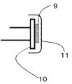
- This figure is a schematic diagram of the neutron beam detection apparatus of the present invention.
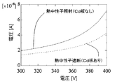
- This figure is a diagram of current-voltage characteristics of the neutron beam detection apparatus of Example 1 when irradiated with thermal neutron rays and shielded.
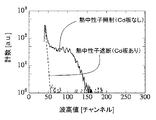
- This figure is a wave height distribution spectrum diagram of the neutron beam detection apparatus of Example 1 when the thermal neutron beam is irradiated and shielded.
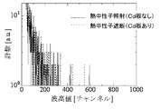
- This figure is a wave height distribution spectrum diagram of the neutron beam detection apparatus of Comparative Example 1 when the thermal neutron beam is irradiated and shielded.
- This figure is the wave height distribution spectrum figure of the neutron beam detection apparatus of the comparative example 2 when a thermal neutron beam is irradiated and shielded.
- This figure is the wave height distribution spectrum figure of the neutron beam detection apparatus of the comparative example 3 when a thermal neutron beam is irradiated and shielded.
- the neutron beam detection apparatus of the present invention comprises a scintillator having a thickness exceeding 1 mm and a silicon photodiode, the scintillator contains only Eu as a lanthanoid, and contains 6 Li of 0.80 atom / nm 3 or more. Furthermore, it consists of a cordierite-type fluoride single crystal having an Eu content of 0.0025 to 0.05 mol%.
- the term “corkyrite” refers to a naturally occurring LiCaAlF 6 compound and has a specific crystal structure.
- the term “corkyrite type” includes a compound having a structure similar to that of corkolite, in which an element in the compound is partially replaced by another element.
- a crystal having a basic structure of a single crystal of a compound represented by the chemical formula M X M Y M Z F 6 (hereinafter, referred to as a “corkyrite basic crystal”) is preferably used as the cordierite fluoride single crystal.
- M X always include Li, Li, Na, K, is at least one kind of element selected from the group consisting of Rb and Cs
- M Y is Ca, Mg, Ba, Sr, from Cd and Be
- M Z is at least one element selected from the group consisting of Al, Ga and In.
- M X are sure you include Li required to detect neutrons. Furthermore, when charge adjustment is performed, it is preferable to include Na.
- the corkyrite type single crystal is a hexagonal crystal belonging to the space group P31c, and can be easily identified by a powder X-ray diffraction technique.
- a single crystal of a compound represented by the chemical formula LiCaAlF 6 , LiSrAlF 6 or LiCa 1-x Sr x AlF 6 (0 ⁇ x ⁇ 1) is easy to produce a large crystal, and a scintillator It is preferable in that it has a high light emission intensity when used as.
- LiCaAlF 6 is most preferable because it has a small effective atomic number and low sensitivity to ⁇ rays.
- the 6 Li content of the cordierite-type fluoride single crystal used in the present invention is required to be 0.80 atom / nm 3 or more from the viewpoint of obtaining sensitivity to neutron rays, which is necessary as a scintillator for detecting neutron rays. Furthermore, in order to increase the sensitivity to neutron rays it is preferably set to the 6 Li content 4atom / nm 3 or more. The upper limit of the 6 Li content is 9 atoms / nm 3 .
- the 6 Li content in the cordierite type fluoride single crystal is theoretically about 9 atom / nm 3 at the maximum, and a 6 Li content higher than this cannot be obtained.
- the above 6 Li content refers to the number of Li elements contained per 1 nm 3 of the cordierite-type fluoride single crystal used in the present invention.
- the incident neutron beam causes a nuclear reaction with 6 Li to generate ⁇ -rays. Therefore, the 6 Li content affects the sensitivity to neutron beams, and the sensitivity to neutron beams increases as the 6 Li content increases.
- Such 6 Li content select a suitable for the composition of the crystalline compound which is a basic structure of the scintillator for neutron detection, or by adjusting the 6 Li content ratio of LiF or the like used as the Li raw material, as appropriate Can be adjusted.
- the 6 Li abundance ratio is the element ratio of 6 Li isotopes with respect to the total Li elements, and the natural abundance ratio is about 7.6%.
- a general-purpose material of the natural abundance ratio as a starting material As a method of adjusting the 6 Li content ratio, a general-purpose material of the natural abundance ratio as a starting material, a method of adjusting by concentrating the said starting material to the desired 6 Li abundance ratio, or pre desired 6 Li presence There is a method in which a concentrated raw material concentrated to a ratio or more is prepared, and the concentrated raw material and the general-purpose raw material are mixed and adjusted.
- the cordierite-type fluoride single crystal used in the present invention is a transparent crystal that is colorless or slightly colored and has good chemical stability. In addition, no deterioration in performance is observed when used for a short period of time under normal use conditions. Furthermore, mechanical strength and workability are also good, and it can be easily processed into a desired shape.
- the scintillator used for this invention can improve the detection sensitivity with respect to a neutron beam by thickening the thickness.
- the thickness of the scintillator indicates the length in the direction perpendicular to the surface to be bonded to the light receiving surface when the scintillator is bonded to the light receiving surface of the silicon photodiode.
- the shape of the scintillator is preferably a rectangular parallelepiped or a cube with the shortest side length exceeding 1 mm, or a disc or columnar shape with a length in the direction perpendicular to the circle exceeding 1 mm.
- the probability of the nuclear reaction between the neutron beam and 6 Li can be improved, and the detection efficiency of the neutron beam can be further increased, which is more preferable.
- the probability of causing a nuclear reaction between a neutron beam and 6 Li increases due to the increase in thickness, not only a thermal neutron beam having a low energy but also a neutron beam having a higher energy than a thermal neutron beam, for example, an epithermal neutron beam. There is also an advantage that it can be detected.
- the upper limit of the thickness is preferably about 200 mm.
- the conventionally known 6 LiF film has a problem of absorbing ⁇ rays inside, and cannot be made as thick as the scintillator of the present invention.
- ⁇ -rays generated by the nuclear reaction quickly react with the luminescent center element and are converted to light, so there is no problem, high neutron beam detection efficiency is obtained, and epithermal neutron beams are also detected. It is very beneficial in that it is possible.
- a specific calculation of the relationship between the thickness of the scintillator of the present invention and the probability of a nuclear reaction is as follows. That is, assuming that a scintillator containing 6 Li of about 9 atoms / nm 3 is irradiated with a thermal neutron beam of 0.025 eV, the reaction cross section of 6 Li and the neutron beam of this scintillator is 940 barn. Under these conditions, when the probability of a neutron beam that causes a nuclear reaction with 6 Li among the irradiated neutron beams is calculated, the probability when the thickness of the scintillator is 1 mm is about 60%.
- the probability when the thickness is 1.5 mm is about 70%, the probability when the thickness is 2 mm is about 80%, and the probability when the thickness is 4 mm is about 90%.
- a scintillator having a nuclear reaction probability exceeding 50% is suitable for practical use.
- the content of 6 Li in the scintillator is reduced or when the detection target is expanded to a high energy neutron beam, for example, an epithermal neutron beam of about 1 eV, it is preferable to make the scintillator thicker.
- the reaction cross section of this Li scintillator with 6 Li and 1 eV neutron beam is 188 barn.
- the thickness of the scintillator is 10 mm, it can be calculated that the probability of a neutron beam that causes a nuclear reaction with 6 Li in the irradiated neutron beam is about 70%.
- the cordierite-type fluoride single crystal used in the present invention contains Eu element in the cordierite-type basic crystal.
- the Eu element is presumed to be present in the inter-lattice of the cordierite-type basic crystal or by replacing some of the elements constituting the crystal, but the exact existence form is unknown.
- ⁇ rays generated by the reaction between the neutron beam and 6 Li react with the Eu element, and light emission containing light in a wavelength region of about 370 nm is obtained.
- Silicon photodiodes generally have the greatest sensitivity to light in the wavelength region of about 900 nm, but have low sensitivity to light in the short wavelength region.
- the silicon photodiode when a scintillator made of a cordierite-type fluoride single crystal containing Eu and a silicon photodiode are combined, the diode can receive the fluorescence emitted by the scintillator. This is considered to be because the intensity of light in the wavelength region of about 370 nm emitted from the scintillator of the present invention is high.
- the content of the Eu element in the cordierite-type fluoride single crystal used in the present invention is 0.0025 mol per mole of the cordierite-type fluoride single crystal used in the present invention from the viewpoint of obtaining a sufficient amount of light emission upon neutron irradiation. % Or more. Moreover, the content of Eu element is 0.05 mol% or less from the viewpoint that single crystal growth is easy and neutron beams with high energy such as epithermal neutron beams can be detected. If the content of Eu element is too large, white turbidity is likely to occur in the single crystal, making it difficult to grow the crystal. Further, it becomes difficult to grow a thick crystal, and it becomes impossible to manufacture a scintillator having a thickness that can detect a high-energy neutron beam.
- the content of Eu element is in the above range, even if the thickness of the scintillator is increased, the amount of emitted light does not decrease so much and the variation in signal intensity can be suppressed.
- the content of Eu element is increased from the above range, the light emission amount is greatly reduced when the thickness of the scintillator is increased, and the signal intensity varies. That is, in the present invention, from the viewpoint of increasing the detection efficiency for thermal neutron beams and detecting high energy neutron beams, the above amount of Eu is used and at the same time the thickness of the scintillator is increased. In general, when there is a lot of Eu in the scintillator, the distance between Eus becomes close.
- the scintillator When the scintillator is thin, there is no particular problem even if the Eu distance is short. However, when the scintillator is thick, the performance as a detection device deteriorates due to the effect of “self-absorption” in which the light emission attenuates. Specifically, when fluorescence is generated by a reaction between Eu and ⁇ rays at a position far from the silicon photodiode in the scintillator, the fluorescence collides with other Eu elements when passing through the scintillator and is attenuated. The Therefore, when the fluorescence is received by the diode, the emission intensity is lowered.
- the fluorescence generated at a position close to the diode immediately reaches the diode, so that it is not easily attenuated, and its emission intensity increases.
- the intensity of light received by the silicon photodiode varies greatly depending on the light emitting position, and the peak value of the electric signal from the silicon photodiode also varies greatly. If the peak values of the electrical signals are different, the range of the peak values indicating that the neutron beam can be detected has to be set wide, and inconveniences such as taking a long time to obtain the detection peak occur.
- the cordierite-type fluoride single crystal used in the present invention contains only Eu as a lanthanoid and does not contain a transition metal and other rare earth elements.
- transition metals mean Ti, V, Cr, Mn, Fe, Co, Ni, Cu and Zn
- other rare earth elements mean Ce, Pr, Nd, Er, Tm, Ho, Dy, Tb, Gd, Sm, Yb, La, Lu, Y, Sc and Pm are meant. This is because if the luminescent center element other than Eu is further contained, inconveniences such as light emission from Eu tend to decrease.
- the solidification rate is an index representing the position in the crystal growth direction, and is determined from the ratio of the weight of the solidified portion to the total weight of the raw material. That is, the position where the solidification rate is 0 represents the first crystallized portion of the obtained crystal, and the position where the solidification rate is 0.1 means using up to 10% by weight of the total weight of the molten raw material. Represents the crystallized part. In the Czochralski method, it is usually 30% by weight or less of the molten raw material that is crystallized.
- the position of the solidification rate 0 corresponds to the uppermost part of the crystal
- the position of the solidification ratio 0.3 corresponds to the lowermost part.
- the effective segregation coefficient the value described in the literature (for example, the growth coefficient may be adopted as an effective segregation coefficient is described in Growth of Ce-doped LiCaAlF 6 and LiSrAlF 6 single crystals by the Czochralski technique under CF 4 atmosphere). Since it varies depending on the method, it is preferable to use a value obtained in advance.
- the effective segregation coefficient of Eu with respect to LiCaAlF 6 obtained by the Czochralski method was 0.025.
- the Eu content (mol%) in the actual crystal can be confirmed by a general elemental analysis technique (for example, ICP mass spectrometry, ICP emission analysis).
- the manufacturing method of the cordierite-type fluoride single crystal used in the present invention is not particularly limited and can be manufactured by a known method, but is preferably manufactured by the Czochralski method.
- the Czochralski method By producing by the Czochralski method, it is possible to produce a cordierite-type fluoride single crystal having excellent quality such as transparency, and it is also possible to produce a large crystal having a diameter of several inches.
- a general method for producing a cordierite-type fluoride single crystal used in the present invention by the Czochralski method will be described with reference to FIG.
- the cordierite-type fluoride single crystal used in the present invention it is preferable to use EuF 3 , M X F, M Y F 2 and M Z F 3 as raw materials. Although these purity is not specifically limited, It is preferable that each is 99.99% or more. Moreover, it is preferable to use a mixed raw material obtained by mixing these raw materials in advance. By using such a mixed raw material, the purity of the crystal can be increased, and characteristics such as emission intensity are improved.
- the mixed raw material may be used in the form of powder or granules, or may be used after being sintered or melted and solidified in advance.
- Concentration concentration is 6 Li content of the scintillator is not particularly limited as long as it is a concentration such that 0.8atom / nm 3 or more, the larger the amount of 6 Li in the scintillator, the neutron beam was grown crystal Since the neutron beam detection efficiency at the time of using as a scintillator for a detection becomes high, the concentrated density
- EuF 3 is blended so as to have a content in the above-described range.
- the weighed value of EuF 3 is preferably set to be larger than the target Eu element content in consideration of the above-described segregation phenomenon.
- the segregation coefficient used when calculating the content of additive elements in the resulting crystal from the weighed value varies depending on the growth conditions such as the type of additive element and the growth rate. It is desirable to determine by examining.
- the raw material powder when using raw material powder with high volatility at high temperature, the raw material powder may be weighed more than the target content and mixed. Since the volatilization amount varies depending on crystal growth conditions (temperature, atmosphere, and process), it is desirable to determine the blending amount by examining the volatilization amount in advance.
- the raw material is filled in the crucible 1.
- the crucible 1, the heater 2, the heat insulating material 3, and the movable stage 4 are set as shown in FIG.
- a double crucible structure may be adopted by installing another crucible with a hole at the bottom on the crucible 1 and fixing the crucible to the heater 2 or the like.
- the seed crystal 5 is attached to the tip of the automatic diameter control device 6.
- a metal having a high melting point such as platinum can be used, but from the viewpoint that the crystallinity of the grown crystal is good, a single crystal having a crystal structure close to that of a cordierite type fluoride single crystal. Is preferably used.
- a LiCaAlF 6 single crystal having a rectangular parallelepiped shape having a size of about 6 mm ⁇ 6 mm ⁇ 30 mm, which is cut, ground, and polished so that a side of 30 mm is along the c-axis direction can be used.
- the automatic diameter control device 6 is a device for measuring the total weight of the seed crystal 5 and the grown crystal and adjusting the pulling speed of the seed crystal 5 from the measured value. When the pulling rate is adjusted, the diameter of the crystal to be grown can be controlled.
- the apparatus 6 may be a pulling apparatus load cell that is commercially available for crystal growth in the Czochralski method.
- the inside of the chamber 7 is evacuated to 1.0 ⁇ 10 ⁇ 3 Pa or less using an evacuation apparatus, and then an inert gas such as high purity argon is introduced into the chamber to perform gas replacement.
- the pressure in the chamber after gas replacement is not particularly limited, but atmospheric pressure is common.
- a solid scavenger such as zinc fluoride or a gas scavenger such as tetrafluoromethane in order to avoid adverse effects due to moisture that cannot be removed even by the gas replacement operation.
- a solid scavenger a method in which the scavenger is premixed in the raw material is suitable.
- a gas scavenger a method of mixing the scavenger with the inert gas and introducing it into the chamber is preferable.
- the raw material is heated and melted by the high frequency coil 8 and the heater 2.
- the heating method is not particularly limited.
- a resistance heating type carbon heater may be used as appropriate.
- the melted raw material melt is brought into contact with the seed crystal 5.
- the crystal is pulled up while adjusting the pulling speed with the automatic diameter control device 6.
- the movable stage 4 may be appropriately moved in the vertical direction in order to adjust the liquid level. While adjusting the output of the high-frequency coil appropriately, it is continuously pulled up, and when the desired length is reached, the crystal is separated from the liquid surface.
- the grown crystal may be annealed for the purpose of removing crystal defects caused by deficiency of fluorine atoms or thermal strain.
- the obtained corklite-type fluoride single crystal can be easily processed into a desired shape.
- a known cutting machine such as a blade saw or a wire saw, a grinding machine, or a polishing machine can be used without any limitation.
- the single crystal can be used as a scintillator by processing and polishing the single crystal into an appropriate shape for the photodetector.
- the shape of the scintillator of the present invention comprising the cordierite fluoride single crystal is not particularly limited, but preferably has a light emitting surface facing a silicon photodiode described later.
- the thickness in the direction perpendicular to the light exit surface needs to exceed 1 mm.
- the thickness of this scintillator it is good also considering the thickness of this scintillator as 1.5 mm or more, 2 mm or more, 4 mm or more, and 10 mm or more.
- the light exit surface is preferably optically polished. By having such a light emitting surface, light generated by the scintillator can be efficiently incident on the silicon photodiode.
- the shape of the light emitting surface is not limited, and a shape corresponding to the application such as a square having a length of several mm to several hundred mm or a circle having a diameter of several mm to several hundred mm is appropriately selected.
- the size is smaller than the light receiving surface of the silicon photodiode because less light is emitted without reaching the light receiving surface.
- the cordierite type fluoride single crystal used in the present invention manufactured as described above is combined with a silicon photodiode to form the neutron beam detection apparatus of the present invention. That is, the light (scintillation light) emitted from the neutron beam detection scintillator of the present invention is converted into an electric signal by a silicon photodiode by irradiating the neutron beam, and the presence and intensity of the neutron beam are captured as an electric signal.
- Any silicon photodiode can be used, but it is preferable to use an APD (avalanche photodiode) having an electric signal amplification function from the viewpoint of receiving light of the scintillator with high sensitivity.
- an avalanche photodiode S8664 series manufactured by Hamamatsu Photonics can be used.
- the light emission surface of the neutron beam detection scintillator of the present invention can be bonded to the light receiving surface of a silicon photodiode with an optional optical grease or the like to obtain a neutron beam detector.
- the light-receiving surface of the diode to which the scintillator is bonded may be covered with a light-shielding material of any material that is difficult to transmit light for the purpose of preventing light from entering the environment.
- the scintillator may be covered with a reflective material made of aluminum, Teflon (registered trademark), barium sulfate, or the like, except for the adhesive surface to the light receiving surface of the silicon photodiode. You may cover the whole with something that has both functions.
- the silicon photodiode can confirm the detection of the neutron beam by observing the output electric signal.
- the electric signal output from the silicon photodiode may be input to an amplifier, a multi-wave height analyzer, or the like and measured by photon counting (photon counting method). It is also possible to check the change in the current value by connecting to an arbitrary current measuring device (for example, a picoammeter) and confirm the change in the current value according to the change in the amount of received light.
- a voltage may be applied to the silicon photodiode in a reverse bias, and in that case, any measuring instrument capable of simultaneously performing voltage and current application and measurement (for example, KEITLEY 237 HIGH VOLTAG SOURCE MEASURE UNIT) may be used.
- the voltage value to be applied is preferably set according to the performance of the silicon photodiode and the flux of neutron to be measured.
- a voltage of 300 to 400V By measuring the relationship between the flux of thermal neutrons irradiated in advance and the current value at the set operating voltage, it can also be used as a neutron beam detector having quantitativeness.
- a neutron beam imaging apparatus can be obtained by bonding the crystal of the present invention to a position sensitive silicon photodiode such as a pixel APD or a CCD camera so as to cover a part or all of the photocathode. .
- An electric signal output from the position-sensitive silicon photodiode can be read out using an arbitrary interface, and may be controlled using a control program of a personal computer.
- Example 1 Manufacture of neutron beam detectors
- the manufacturing method of the neutron beam detection apparatus of this invention used in Example 1 is demonstrated.
- a corklite-type fluoride single crystal used in the present invention was manufactured.
- raw materials high purity fluoride powders of LiF, CaF 2 , AlF 3 and EuF 3 with a purity of 99.99% or more were used.
- LiF 6 Li content ratio was used as 95%.
- the crucible 1 the heater 2, and the heat insulating material 3, those made of high purity carbon were used.
- each raw material is as follows: LiF 393.1 g, CaF 2 1224.4 g, AlF 3 1317.0 g, EuF 3 65.5 g, And mixed well to obtain a mixed raw material.
- the mixed raw material was filled in the crucible 1.
- the crucible 1 filled with the mixed raw material was placed on the movable stage 4, and the heater 2 and the heat insulating material 3 were sequentially set around the crucible 1.
- the LiCaAlF 6 single crystal was cut, ground, and polished so that a side of 30 mm along the c-axis direction was formed in a 6 mm ⁇ 6 mm ⁇ 30 mm rectangular parallelepiped shape, and a seed crystal 5 was obtained.
- the seed crystal 5 was attached to the tip of an automatic diameter control device 6.
- the inside of the chamber 6 was evacuated to 5.0 ⁇ 10 ⁇ 4 Pa using an evacuation apparatus composed of an oil rotary pump and an oil diffusion pump. Thereafter, a mixed gas of tetrafluoromethane-argon was introduced into the chamber 7 until the pressure in the chamber reached atmospheric pressure, and gas replacement was performed. A high frequency current was applied to the high frequency coil 8, and the raw material was heated and melted by induction heating. The seed crystal 5 was moved and brought into contact with the liquid surface of the melted raw material melt. After adjusting the output of the heater 2 so that the temperature at which the part in contact with the seed crystal 5 is solidified, the automatic diameter control device 6 sets the target to a diameter of 55 mm and pulls up the crystal while automatically adjusting the pulling speed. It was.
- the crystal was continuously pulled up while appropriately moving the movable stage 4 and adjusting the output of the high-frequency coil as appropriate in order to adjust the liquid level to be constant. When the length became 60 mm, the crystal was cut off from the liquid surface. The crystal was cooled over 48 hours to obtain a LiCaAlF 6 single crystal containing Eu having a diameter of 55 mm and a length of 60 mm.
- the obtained crystal was cut with a wire saw equipped with a diamond wire, ground and mirror-polished, and processed into a rectangular parallelepiped shape of length ⁇ width ⁇ thickness of 10 mm ⁇ 10 mm ⁇ 2 mm.
- the crystals after processing, cut out from the from the [Equation 2] the content C s is (site of solidification rate g corresponding to an initial step in the single crystal growth is 0.01) 0.05 mol% and becomes part of Eu, the present invention A scintillator was obtained.
- the amount C 0 of Eu in the raw material was 2 mol%, and the value of the effective segregation coefficient k was 0.025.
- the 6 Li content in this portion was 8.3 atoms / nm 3 .
- the effective atomic number was 15.
- the obtained scintillator 9 for neutron beam detection is optically greased (Applied Koken Kogyo Co., Ltd. 6262A) on the light receiving surface of a silicon photodiode 10 (S8664-1010 manufactured by Hamamatsu Photonics).
- the neutron beam detection apparatus of the present invention was obtained by bonding and covering the whole with a light shielding material 11 made of a black vinyl sheet.
- a thermal neutron beam detection test was performed using the neutron beam detection apparatus of the present invention.
- the thermal neutron radiation source a sealed radiation source 252 Cf placed in a 50 mm thick polyethylene container was used.
- thermal neutron beam irradiation When the thermal neutron beam is irradiated without inserting anything between the thermal neutron beam source and the device (hereinafter referred to as thermal neutron beam irradiation), and when the thermal neutron beam is irradiated with the shielding plate inserted
- thermal neutron radiation shielding As the shielding plate, a Cd (cadmium) plate having a thickness of 1 mm that absorbs thermal neutron rays was used.
- the current value at the time of thermal neutron beam irradiation is larger than the value at the time of shielding.
- the current value at 350V was 2.13 ⁇ 10 ⁇ 8 A at the time of thermal neutron ray shielding, whereas at the time of thermal neutron beam irradiation 3.14 ⁇ 10 ⁇ 8 A. This indicates that the current value increases as the thermal neutron flux increases. From the above, it was confirmed that the thermal neutron beam can be detected by the neutron beam detection apparatus of the present invention by simple measurement of current-voltage characteristics.
- the pulse height distribution spectra at the time of thermal neutron beam irradiation and thermal neutron beam shielding were compared.
- the thermal neutron radiation source as described above, a 252 Cf sealed radiation source in a polyethylene container was used.
- the pulse height distribution spectrum was measured while applying a voltage of 3.2 V with a reverse bias.
- the electrical signal output from the neutron beam detection apparatus of the present invention is a pulse signal reflecting scintillation light.
- the pulse height represents the emission intensity of the scintillation light.
- the pulse waveform exhibits an attenuation curve based on the attenuation time constant of the scintillation light.
- FIG. 4 shows a wave height distribution spectrum at the time of thermal neutron beam irradiation and thermal neutron beam shielding.
- the horizontal axis of the pulse height distribution spectrum represents the peak value of the electric signal, that is, the emission intensity of the scintillation light.
- the vertical axis represents the frequency of the electrical signal indicating each peak value.
- a scintillator made of a single crystal of Ce 0.04%: LiCaAlF 6 was used.
- the effective atomic number was 15.
- the pulse height distribution spectrum was measured while applying a voltage of 310 V with a reverse bias, in the same manner as in Example 1, at the time of thermal neutron beam irradiation and thermal neutron beam shielding.
- a wave height distribution spectrum was obtained.
- FIG. 5 shows the obtained pulse height distribution spectrum.
- Each raw material is as follows: LiF 397.6g, 1238.7 g CaF 2 , AlF 3 1332.3 g, PrF 3 31.4 g, And a portion where the Pr content C s is 0.04 mol% from the above [Formula 2] (a portion where the solidification rate g corresponding to the initial stage in single crystal growth is 0.01).
- a neutron beam detector was manufactured in the same manner as in Example 1 except that the device was cut out from the above.
- the amount C 0 of Pr in the raw material was 1 mol%, and the value of the effective segregation coefficient k was 0.04.
- a scintillator made of a single crystal of Pr 0.04%: LiCaAlF 6 was used.
- the effective atomic number was 15.
- the pulse height distribution spectrum was measured while applying a voltage of 310 V with a reverse bias, in the same manner as in Example 1, at the time of thermal neutron beam irradiation and thermal neutron beam shielding.
- a wave height distribution spectrum was obtained.
- FIG. 6 shows the obtained pulse height distribution spectrum.
- each raw material is as follows: LiF 437.3g, YF 3 2545.5 g, CeF 3 17.2 g, Weighed as described, and, (site of solidification rate g corresponding to an initial step in the single crystal growth is 0.01) the resulting crystals Ce content than [Equation 2] C s is 0.5 mol% portion serving
- a neutron beam detector was manufactured in the same manner as in Example 1 except that the device was cut out from the above.
- the amount C 0 of Ce in the raw material was 0.5 mol%, and the value of the effective segregation coefficient k was 1.
- a scintillator composed of a single crystal of Ce 0.5%: LiYF 4 was used.
- the effective atomic number was 33.
- the pulse height distribution spectrum was measured while applying a voltage of 310 V with a reverse bias, in the same manner as in Example 1, at the time of thermal neutron beam irradiation and thermal neutron beam shielding.
- a wave height distribution spectrum was obtained.
- FIG. 7 shows the obtained pulse height distribution spectrum.
- Example 1 the wave height distribution spectrum at the time of thermal neutron beam irradiation and the wave height distribution spectrum at the time of thermal neutron beam shielding were clearly different (see FIG. 4). Specifically, the frequency of the electrical signal at each peak value (75 to 150 channels) at the time of thermal neutron beam irradiation is higher than that at the time of thermal neutron beam shielding, that is, each peak value (75 It was found that the frequency of electrical signals in ( ⁇ 150 channels) increases. On the other hand, in Comparative Examples 1 to 3, no clear difference was observed between thermal neutron beam irradiation and thermal neutron beam shielding, and the frequency of electrical signals was low in any case (see FIGS. 5 to 7).
- the neutron beam detection apparatus of the present invention can detect the thermal neutron beam.
- a scintillator used in the neutron beam detector a corkyrite type single crystal containing only Eu as a lanthanoid is suitable, and a crystal containing other rare earth such as Ce or Pr is not suitable. .
- the emission intensity at a short wavelength is high, but in a scintillator containing other elements, the emission intensity is considered to be low.
Abstract
Description
具体的には、特許文献1において、Ti等の第4周期元素を含み、且つ、6Liを0.80atom/nm3以上含有するコルキライト型フッ化物単結晶であって、更に、Ce又は/及びEuを含有するコルキライト型フッ化物単結晶からなる中性子線検出用シンチレーターを提案している。特許文献1のシンチレーターは、第4周期元素を含むことによって長波長の光を発するので、シリコンフォトダイオードと組み合わせることができるだけでなく、Ce又は/及びEuを含むことによって短波長の光を発するので、光電子増倍管とも組み合わせることができる。
特許文献2においては、少なくとも二種類の希土類元素を含有し、6Liを0.80atom/nm3以上含有するコルキライト型フッ化物単結晶からなる中性子線検出用シンチレーターを提案している。特許文献2のシンチレーターは、希土類元素としてCe及び/又はEuを含有することで、短波長の光を発し、光電子増倍管と組み合わせることができ、また、Ce、Eu以外の希土類元素を含有することで長波長の光を発し、シリコンフォトダイオードとも組み合わせることができる。
特許文献3においては、リチウム及びII価以上の金属元素を含むフッ化物結晶であって、1.1~20atom/nm3の6Liを含み、有効原子番号が10~40であり、且つ、Eu等のランタノイドを含む金属フッ化物結晶からなるシンチレーターを提案している。
中性子線の検出効率は、照射された中性子線のうち核反応を起こす中性子線の割合、中性子線と6Liとの反応により生じたα線がシンチレーター内で吸収されるか否か、及びα線と発光中心元素との反応で生じる光が濃度消光により減衰するか否か等の複数の要因により左右される。
従って、シンチレーターの厚みを厚くしたときに、薄い場合に比べて、必ずしもシンチレーターとしての性能が向上するとは限らない。濃度消光の及ぼす影響、加工容易性、シンチレーターを構成する結晶の透明性等により、検出効率が低下したり、或いは、検出効率以外の性能が低下する可能性が高いからである。そのため、適切な構成元素や基本構造をなす結晶の種類、厚み等を検討して、実際にシンチレーターを作製し、更にシンチレーターとしての各種性能を評価するまでは、どのような特徴のシンチレーターが得られるかを予測するのは困難である。
前記単結晶が、Euのみを含んでおり、かつ、6Liを0.80atom/nm3以上含有し、
さらに、Euの含有量が0.0025乃至0.05mol%であり、
前記シンチレーターの厚みが1mmを超えていることを特徴とする中性子線検出装置が提供される。
なお、コルキライトとは、天然に存在するLiCaAlF6化合物をいい、特有の結晶構造を有する。また、コルキライト型といった場合には、コルキライトに類似した構造を有する化合物であって、該化合物中の元素が他の元素に一部置き換わったものも含む。
当該コルキライト型単結晶は、空間群P31cに属する六方晶であって、粉末X線回折の手法によって容易に同定することができる。
前記コルキライト型基本結晶の中でも、化学式LiCaAlF6、LiSrAlF6又はLiCa1-xSrxAlF6(0<x<1)で表わされる化合物の単結晶が、大型の結晶を作製しやすく、また、シンチレーターとして用いる際の発光強度が高いという点で、好ましい。中でもLiCaAlF6は、有効原子番号が小さく、γ線に対する感度が低いため、最も好ましい。
有効原子番号=(ΣWiZi 4)1/4
式中、
Wiは、シンチレーターを構成する元素のうちのi番目の元素の質量
分率、
Ziは、シンチレーターを構成する元素のうちのi番目の元素の原子
番号、
で定義される指標である。
6Li含有量の上限は9atom/nm3である。コルキライト型フッ化物単結晶における6Li含有量は、理論上最大で9atom/nm3程度であり、これ以上の6Li含有量のものを得ることはできない。
本発明において、上記6Li含有量とは、本発明に用いるコルキライト型フッ化物単結晶1nm3あたりに含まれるLi元素の個数をいう。入射した中性子線は、6Liと核反応を起こしてα線を生じさせる。従って、該6Li含有量は中性子線に対する感度に影響し、6Li含有量が多いほど中性子線に対する感度が向上する。
6Li含有量=A×C×ρ×10-23/M 〔式1〕
式中、
Aは、アボガドロ数[6.02×10²³]、
Cは、Li元素中の6Li存在比率[%]、
ρは、本発明に用いるコルキライト型フッ化物単結晶の密度
[g/cm3]、
Mは、分子量[g/mol]、
によって求めることができる。
即ち、6Liを9atom/nm3程度含有するシンチレーターに、0.025eVの熱中性子線を照射すると仮定すると、このシンチレーターの、6Liと中性子線との反応断面積は940barnである。これらの条件の下、照射した中性子線のうち6Liと核反応を起こす中性子線の確率を算出すると、該シンチレーターの厚みが1mmのときの確率は約60%となる。厚みが1.5mmのときの確率は約70%であり、厚みが2mmのときの確率は約80%であり、厚みが4mmのときの確率は約90%である。一般に、核反応の確率が50%を超えるシンチレーターは、実用化に適している。
ただし、シンチレーター中の6Li含有量を少なくする場合や、エネルギーの高い中性子線、例えば約1eVの熱外中性子線まで検出対象を広げる場合は、シンチレーターをより厚い厚みにすることが好ましい。6Liを9atom/nm3含有する本発明のシンチレーターに、1eVの熱外中性子線を照射すると仮定すると、このシンチレーターの、6Liと1eVの中性子線との反応断面積は、188barnである。これらの条件の下、シンチレーターの厚みが10mmのとき、照射した中性子線のうち6Liと核反応を起こす中性子線の確率は約70%であることが、算出できる。
即ち、本発明においては、熱中性子線に対する検出効率を高めたり、高エネルギーの中性子線を検出するという観点から、上記の量のEuを用いると同時に、シンチレーターの厚みを厚くする。一般に、シンチレーター内にEuが多く存在すると、Eu同士の距離が近くなる。シンチレーターが薄い場合は、Euの距離が近くても特に問題は生じないが、シンチレーターが厚いと、発光が減衰する「自己吸収」という現象の影響により、検出装置としての性能が悪くなる。
具体的には、シンチレーター内のシリコンフォトダイオードから遠い位置において、Euとα線との反応により蛍光が生じると、該蛍光は、シンチレーター内を通過する際に他のEu元素に衝突し、減衰される。そのため、該蛍光を該ダイオードで受光する際に、発光強度が低くなる。逆に、ダイオードと近い位置で生じた蛍光は、すぐにダイオードに到達するので、減衰されにくく、その発光強度は高くなる。このように、発光位置によって、シリコンフォトダイオードが受光する光の強度が大きく異なり、シリコンフォトダイオードからの電気信号の波高値も大きく異なる。電気信号の波高値が異なると、中性子線が検出できていることを示す波高値の範囲を広く設定せねばならず、また、検出ピークを得るまでに長時間を要する、等の不都合が生じる。
Cs=kC0(1-g)k-1 〔式2〕
式中、
Csは本発明に用いるコルキライト型フッ化物単結晶中のEuの含有量
[mol%]、
kは実効偏析係数、
C0は原料中のEuの量[mol%]、
gは固化率、
に基づいて原料中のEu含有量(C0の値)を調整すれば、所望の量のEuを含有するコルキライト型フッ化物単結晶を容易に得ることができる。
尚、本発明において、固化率は、結晶の成長方向における位置を表す指標であり、原料全体の重量に対して固化している部分の重量が占める割合から求められる。即ち、固化率0の位置とは、得られた結晶のうち最初に結晶化された部分を表し、固化率0.1の位置とは、溶融原料全体の重量の10重量%までを使用して結晶化された部分を表す。チョクラルスキー法は通常、結晶化させるのは溶融原料の30重量%以下である。例えば、チョクラルスキー法により溶融原料の30重量%を結晶化して製造された結晶においては、固化率0の位置は結晶の最上部にあたり、固化率0.3の位置は最下部にあたる。
実際の結晶中のEuの含有量(mol%)は、一般的な元素分析の手法(例えば、ICP質量分析、ICP発光分析)によって確認できる。
以下、チョクラルスキー法によって本発明に用いるコルキライト型フッ化物単結晶を製造する際の、一般的な方法について、図1に基づき説明する。
EuF3は、前記した範囲の含有量となるように配合する。具体的には、EuF3の秤量値は、前記した偏析現象を考慮し、目標とするEu元素の含有量よりも多く設定することが好ましい。得られる結晶中の添加元素の含有量を秤量値から算出する際に用いる偏析係数は、添加元素の種類や成長速度など育成条件によって変動するため、結晶作製条件ごとに元素分析などで実際の濃度を調べて決定することが望ましい。
また、高温で揮発性が高い原料粉末を用いる場合は、該原料粉末を、目標とする含有量よりも多く秤量し、混合しても良い。揮発量は、結晶育成条件(温度・雰囲気・工程)によって異なるため、予め揮発量を調べて配合量を決めることが望ましい。
次に、種結晶5を自動直径制御装置6の先端に取り付ける。種結晶5としては、白金などの高融点の金属を用いることもできるが、育成した結晶の結晶性が良好であるという観点から、コルキライト型フッ化物単結晶もしくはそれと近い結晶構造を持った単結晶を用いることが好ましい。例えば、LiCaAlF6単結晶を6mm×6mm×30mm程度のサイズの直方体形状であって、30mmの辺がc軸方向に沿うように切断、研削、研磨したものを用いることができる。自動直径制御装置6は、種結晶5と育成された結晶との合計重量を測定し、その測定値から種結晶5の引き上げ速度を調整するための装置である。引き上げ速度を調整すると、育成する結晶の直径を制御することができる。該装置6では、チョクラルスキー法の結晶育成用に市販されている引上装置用ロードセルを用いることができる。
なお、前記光出射面の形状は限定されず、一辺の長さが数mm~数百mmの四角形、或いは直径が数mm~数百mmの円など、用途に応じた形状を適宜選択して用いることができるが、シリコンフォトダイオードの受光面よりも小さい方が、受光面に届かずに散逸する発光が少ないため、好ましい。
また、シリコンフォトダイオードに対向しない面には、アルミニウム或いはテフロン(登録商標)等からなる光反射膜を施すことが好ましい。シンチレーターで生じた光の散逸を防止することができるからである。
即ち、中性子線の照射により、本発明の中性子線検出用シンチレーターから発せられた光(シンチレーション光)を、シリコンフォトダイオードによって電気信号に変換することによって、中性子線の有無及び強度を電気信号として捉えることができる。
シリコンフォトダイオードとしては任意のものを用いることができるが、高感度にシンチレーターの光を受光できるという観点から、電気信号の増幅機能を有するAPD(アバランシェフォトダイオード)を用いることが好ましい。一例を挙げると、浜松ホトニクス社製アバランシェフォトダイオードS8664シリーズを用いることができる。
更に、ピクセルAPDやCCDカメラのように位置敏感型のシリコンフォトダイオードに、本発明の結晶を、光電面の一部または全部を覆うように接合することで、中性子線撮像装置とすることができる。位置敏感型のシリコンフォトダイオードから出力される電気信号は、任意のインターフェイスを用いて読み出すことができ、パーソナルコンピューターの制御用プログラムを用いて制御してもよい。
(中性子線検出装置の製造)
以下、実施例1で用いられる、本発明の中性子線検出装置の製造方法を説明する。
図1に示すチョクラルスキー法による結晶製造装置を用いて、本発明に用いるコルキライト型フッ化物単結晶を製造した。原料としては、純度が99.99%以上のLiF、CaF2、AlF3及びEuF3の高純度フッ化物粉末を用いた。なお、LiFとしては、6Li存在比率が95%のものを用いた。坩堝1、ヒーター2、及び断熱材3としては、高純度カーボン製のものを使用した。
まず、各原料を以下;
LiF 393.1g、
CaF2 1224.4g、
AlF3 1317.0g、
EuF3 65.5g、
の通りに秤量し、よく混合して混合原料を得た。該混合原料を坩堝1に充填した。
混合原料を充填した坩堝1を、可動ステージ4上に設置し、その周囲にヒーター2及び断熱材3を順次セットした。次にLiCaAlF6単結晶を、6mm×6mm×30mmの直方体形状で30mmの辺がc軸方向に沿うように切断、研削、研磨して、種結晶5を得た。該種結晶5を、自動直径制御装置6の先端に取り付けた。
高周波コイル8に高周波電流を印加し、誘導加熱によって原料を加熱して溶融させた。種結晶5を移動し、溶融した原料融液の液面に接触させた。種結晶5と接触した部分が凝固する温度となるようヒーター2の出力を調整した後、自動直径制御装置6により、直径55mmを目標に設定して、引き上げ速度を自動調整しながら、結晶を引き上げた。
液面高さが一定となるよう調整するため可動ステージ4を適宜動かしながら、且つ、高周波コイルの出力を適宜調整しながら、結晶を連続的に引き上げた。60mmの長さとなったところで、結晶を液面から切り離した。該結晶を48時間かけて冷却することで、直径55mm、長さ60mmの、Euを含有するLiCaAlF6単結晶を得た。
加工後の結晶を、前記〔式2〕より、Euの含有量Csが0.05mol%となる部分(単結晶育成において初期段階にあたる固化率gが0.01の部位)から切り出し、本発明のシンチレーターを得た。このとき、原料中のEuの量C0は2mol%であり、実効偏析係数kの値は0.025であった。〔式1〕より、この部分における6Li含有量は、8.3atom/nm3であった。有効原子番号は15であった。
次に、本発明の中性子線検出装置を用い、熱中性子線の検出試験を行った。熱中性子線源としては、密封線源の252Cfを50mm厚のポリエチレンの容器に入れたものを用いた。熱中性子線源と該装置の間に何も挿入せずに熱中性子線を照射する場合(以下、熱中性子線照射時と呼ぶ)、及び遮蔽板を挿入した状態で熱中性子線を照射する場合(以下、熱中性子線遮蔽時と呼ぶ)の、電流電圧特性及び波高分布スペクトルを測定した。遮蔽板としては、熱中性子線を吸収する厚み1mmのCd(カドミウム)の板を用いた。
本発明の中性子線検出装置を用いて、熱中性子線照射時、及び熱中性子線遮蔽時の電流電圧特性を比較した。
該中性子線検出装置は、電流計と接続して用いた。電流計としては、電圧を印加しながら電流値を読み取ることのできるKEITHLEY 237 HIGH VOLTAGE SOURCE MEASURE UNITを用いた。パーソナルコンピューター上の制御プログラムにより、逆バイアスで300~400Vの電圧を印加しながら電流値の計測を行い、電流電圧特性のグラフを描画した。
熱中性子線源としては、前記した通り、252Cf密封線源をポリエチレン容器に入れたものを用いた。図3に、熱中性子線照射時及び熱中性子線遮蔽時の、電流電圧特性を示す。熱中性子線照射時の電流値は、遮蔽時の値より大きく、例えば350Vにおける電流値は、熱中性子線遮蔽時は2.13×10⁻⁸Aだったのに対し、熱中性子線照射時は3.14×10⁻⁸Aであった。このことから、熱中性子のフラックスの増加に伴って電流値が増加することがわかった。
以上により、簡便な電流電圧特性の測定によって、本発明の中性子線検出装置で熱中性子線の検出が可能であることが確認された。
本発明の中性子線検出装置を用いて、熱中性子線照射時、及び熱中性子線遮蔽時の波高分布スペクトルを比較した。
熱中性子線源としては、前記した通り、252Cf密封線源をポリエチレン容器に入れたものを用いた。逆バイアスで3.2Vの電圧を印加しながら波高分布スペクトルを測定した。
本発明の中性子線検出装置より出力される電気信号は、シンチレーション光を反映したパルス状の信号である。パルスの波高は、シンチレーション光の発光強度を表す。また、パルスの波形は、シンチレーション光の減衰時定数に基づいた減衰曲線を呈する。出力された電気信号を、整形増幅器で整形及び増幅した後、多重波高分析器に入力して解析することで、波高分布スペクトルを作成した。
図4に、熱中性子線照射時及び熱中性子線遮蔽時の、波高分布スペクトルを示す。
該波高分布スペクトルの横軸は、電気信号の波高値、すなわちシンチレーション光の発光強度を表している。また、縦軸は各波高値を示した電気信号の頻度を表す。
各原料を以下;
LiF 397.7g、
CaF2 1238.7g、
AlF3 1332.4g、
CeF3 31.3g、
の通りに秤量し、且つ、得られた結晶を前記〔式2〕よりCe含有量Csが0.04mol%となる部分(単結晶育成において初期段階にあたる固化率gが0.01の部位)から切り出した以外、実施例1と同様にして中性子線検出装置を製造した。原料中のCeの量C0は1mol%であり、実効偏析係数kの値は0.04であった。該装置においては、Ce0.04%:LiCaAlF6の単結晶からなるシンチレーターが用いられた。有効原子番号は15であった。
得られた中性子線検出装置を用いて、逆バイアスで310Vの電圧を印加しながら波高分布スペクトルを測定した以外、実施例1と同様にして、熱中性子線照射時、及び熱中性子線遮蔽時の波高分布スペクトルを得た。図5に、得られた波高分布スペクトルを示す。
各原料を以下;
LiF 397.6g、
CaF2 1238.7g、
AlF3 1332.3g、
PrF3 31.4g、
の通りに秤量し、且つ、得られた結晶を前記〔式2〕よりPr含有量Csが0.04mol%となる部分(単結晶育成において初期段階にあたる固化率gが0.01の部位)から切り出した以外、実施例1と同様にして中性子線検出装置を製造した。原料中のPrの量C0は1mol%であり、実効偏析係数kの値は0.04であった。該装置においては、Pr0.04%:LiCaAlF6の単結晶からなるシンチレーターが用いられた。有効原子番号は15であった。
得られた中性子線検出装置を用いて、逆バイアスで310Vの電圧を印加しながら波高分布スペクトルを測定した以外、実施例1と同様にして、熱中性子線照射時、及び熱中性子線遮蔽時の波高分布スペクトルを得た。図6に、得られた波高分布スペクトルを示す。
各原料を以下;
LiF 437.3g、
YF3 2545.5g、
CeF3 17.2g、
の通りに秤量し、且つ、得られた結晶を前記〔式2〕よりCe含有量Csが0.5mol%となる部分(単結晶育成において初期段階にあたる固化率gが0.01の部位)から切り出した以外、実施例1と同様にして中性子線検出装置を製造した。原料中のCeの量C0は0.5mol%であり、実効偏析係数kの値は1であった。該装置においては、Ce0.5%:LiYF4の単結晶からなるシンチレーターが用いられた。有効原子番号は33であった。
得られた中性子線検出装置を用いて、逆バイアスで310Vの電圧を印加しながら波高分布スペクトルを測定した以外、実施例1と同様にして、熱中性子線照射時、及び熱中性子線遮蔽時の波高分布スペクトルを得た。図7に、得られた波高分布スペクトルを示す。
一方、比較例1~3では、熱中性子線照射時と熱中性子線遮蔽時とで、明瞭な差異は見られず、何れの場合も電気信号の頻度が少なかった(図5~7参照)。このことは、熱中性子線を照射しても、比較例1~3の中性線検出装置では、中性子線を検出することができないことを表している。
以上により、波高分布スペクトルの測定結果からも、本発明の中性子線検出装置で熱中性子線の検出が可能であることが確認された。また、中性子線検出装置に用いるシンチレーターとしては、ランタノイドとしてEuのみを含有させたコルキライト型単結晶が適しており、CeやPrといったその他の希土類を含有させた結晶は、適さないことが確認された。Euを含有させたシンチレーターの場合、短波長の発光強度が高いが、その他の元素を含有させたシンチレーターでは、発光強度が弱いことが原因であると考えられる。
2 ヒーター
3 断熱材
4 可動ステージ
5 種結晶
6 自動直径制御装置
7 チャンバー
8 高周波コイル
9 中性子線検出用シンチレーター
10 シリコンフォトダイオード
11 遮光材
Claims (2)
- コルキライト型フッ化物単結晶からなる中性子線検出用シンチレーターとシリコンフォトダイオードとを備えた中性子線検出装置であって、
前記単結晶が、ランタノイドとしてEuのみを含んでおり、かつ、6Liを0.80atom/nm3以上含有し、
更に、Euの含有量が0.0025乃至0.05mol%であり、
前記シンチレーターの厚みが1mmを超えていることを特徴とする中性子線検出装置。 - 前記単結晶が、LiCaAlF6、LiSrAlF6又はLiCa1-xSrxAlF6(0<x<1)で表わされる組成の基本単結晶中にEuを含有している、請求項1に記載の中性子線検出装置。
Priority Applications (3)
| Application Number | Priority Date | Filing Date | Title |
|---|---|---|---|
| EP12754361.9A EP2685286A4 (en) | 2011-03-08 | 2012-03-08 | NEUTRON BEAM DETECTION DEVICE |
| US13/985,963 US20130320217A1 (en) | 2011-03-08 | 2012-03-08 | Neutron detection device |
| JP2013503611A JPWO2012121346A1 (ja) | 2011-03-08 | 2012-03-08 | 中性子線検出装置 |
Applications Claiming Priority (2)
| Application Number | Priority Date | Filing Date | Title |
|---|---|---|---|
| JP2011-050731 | 2011-03-08 | ||
| JP2011050731 | 2011-03-08 |
Publications (1)
| Publication Number | Publication Date |
|---|---|
| WO2012121346A1 true WO2012121346A1 (ja) | 2012-09-13 |
Family
ID=46798300
Family Applications (1)
| Application Number | Title | Priority Date | Filing Date |
|---|---|---|---|
| PCT/JP2012/056009 WO2012121346A1 (ja) | 2011-03-08 | 2012-03-08 | 中性子線検出装置 |
Country Status (4)
| Country | Link |
|---|---|
| US (1) | US20130320217A1 (ja) |
| EP (1) | EP2685286A4 (ja) |
| JP (1) | JPWO2012121346A1 (ja) |
| WO (1) | WO2012121346A1 (ja) |
Cited By (2)
| Publication number | Priority date | Publication date | Assignee | Title |
|---|---|---|---|---|
| EP3064965A4 (en) * | 2013-10-28 | 2017-06-07 | Tokuyama Corporation | Neutron scintillator and neutron detector |
| WO2017158912A1 (ja) * | 2016-03-17 | 2017-09-21 | 株式会社日立製作所 | 放射線測定用プローブ |
Families Citing this family (5)
| Publication number | Priority date | Publication date | Assignee | Title |
|---|---|---|---|---|
| US9240523B2 (en) * | 2009-04-03 | 2016-01-19 | Osram Opto Semiconductors Gmbh | Method for producing an optoelectronic component, optoelectronic component, and component arrangement having a plurality of optoelectronic components |
| WO2013003349A2 (en) * | 2011-06-26 | 2013-01-03 | Schlumberger Canada Limited | Scintillator-based neutron detector for oilfield applications |
| JP6223881B2 (ja) * | 2014-03-18 | 2017-11-01 | 株式会社東芝 | 光検出器 |
| US10125312B2 (en) * | 2016-09-06 | 2018-11-13 | Ut-Battelle, Llc | Divalent-ion-doped single crystal alkali halide scintillators |
| US11774630B2 (en) | 2021-03-12 | 2023-10-03 | Baker Hughes Oilfield Operations Llc | Systems and methods for determining clean inelastic and capture spectra |
Citations (2)
| Publication number | Priority date | Publication date | Assignee | Title |
|---|---|---|---|---|
| WO2009119378A1 (ja) | 2008-03-24 | 2009-10-01 | 株式会社トクヤマ | 中性子検出用シンチレーターおよび中性子検出装置 |
| WO2011115179A1 (ja) * | 2010-03-19 | 2011-09-22 | 株式会社トクヤマ | 中性子検出用シンチレーター、中性子線検出器及び中性子線撮像装置 |
Family Cites Families (3)
| Publication number | Priority date | Publication date | Assignee | Title |
|---|---|---|---|---|
| US4636644A (en) * | 1984-05-01 | 1987-01-13 | Irt Corporation | Anti-parallax scintillator system for use with penetrating ionizing radiation |
| US20130214203A1 (en) * | 2010-11-02 | 2013-08-22 | Tohoku University | Metal fluoride crystal and light-emitting device |
| JPWO2012115234A1 (ja) * | 2011-02-24 | 2014-07-07 | 株式会社トクヤマ | 中性子検出用シンチレーター及び中性子線検出器 |
-
2012
- 2012-03-08 JP JP2013503611A patent/JPWO2012121346A1/ja not_active Withdrawn
- 2012-03-08 US US13/985,963 patent/US20130320217A1/en not_active Abandoned
- 2012-03-08 EP EP12754361.9A patent/EP2685286A4/en not_active Withdrawn
- 2012-03-08 WO PCT/JP2012/056009 patent/WO2012121346A1/ja active Application Filing
Patent Citations (2)
| Publication number | Priority date | Publication date | Assignee | Title |
|---|---|---|---|---|
| WO2009119378A1 (ja) | 2008-03-24 | 2009-10-01 | 株式会社トクヤマ | 中性子検出用シンチレーターおよび中性子検出装置 |
| WO2011115179A1 (ja) * | 2010-03-19 | 2011-09-22 | 株式会社トクヤマ | 中性子検出用シンチレーター、中性子線検出器及び中性子線撮像装置 |
Non-Patent Citations (3)
| Title |
|---|
| J. SCHELTEN, PHYSICAB: CONDENSED MATTER, vol. 234-236, 1997, pages 1084 - 1086 |
| K. NITTOH: "Nuclear Instruments and Methods in Physics Research Section A Accelerators", SPECTROMETERS, DETECTORS AND ASSOCIATED EQUIPMENT, vol. 605, no. 1-2, 2009, pages 107 - 110 |
| See also references of EP2685286A4 |
Cited By (2)
| Publication number | Priority date | Publication date | Assignee | Title |
|---|---|---|---|---|
| EP3064965A4 (en) * | 2013-10-28 | 2017-06-07 | Tokuyama Corporation | Neutron scintillator and neutron detector |
| WO2017158912A1 (ja) * | 2016-03-17 | 2017-09-21 | 株式会社日立製作所 | 放射線測定用プローブ |
Also Published As
| Publication number | Publication date |
|---|---|
| JPWO2012121346A1 (ja) | 2014-07-17 |
| EP2685286A4 (en) | 2014-09-10 |
| EP2685286A1 (en) | 2014-01-15 |
| US20130320217A1 (en) | 2013-12-05 |
Similar Documents
| Publication | Publication Date | Title |
|---|---|---|
| RU2494416C2 (ru) | Сцинтиллятор для детектирования нейтронов и нейтронный детектор | |
| WO2012011506A1 (ja) | ホスウィッチ型熱中性子検出器 | |
| WO2012121346A1 (ja) | 中性子線検出装置 | |
| WO2011145651A1 (ja) | 中性子線検出器、中性子線検出用シンチレーターおよび中性子線とγ線とを弁別する方法 | |
| WO2011136224A1 (ja) | 中性子用シンチレーターおよび中性子検出器 | |
| US9920243B2 (en) | Scintillator, radiation detector, and method for detecting radiation | |
| Glodo et al. | Mixed lutetium iodide compounds | |
| WO2011115179A1 (ja) | 中性子検出用シンチレーター、中性子線検出器及び中性子線撮像装置 | |
| JP5877417B2 (ja) | 中性子検出用シンチレーター及び中性子線検出器 | |
| JP5868329B2 (ja) | 中性子シンチレーター | |
| WO2012115234A1 (ja) | 中性子検出用シンチレーター及び中性子線検出器 | |
| JP5634285B2 (ja) | コルキライト型結晶、中性子検出用シンチレーター及び中性子線検出器 | |
| JP5889202B2 (ja) | 金属フッ化物共晶体、中性子用シンチレーター及び中性子撮像装置 | |
| JP5737978B2 (ja) | 中性子検出用シンチレーター及び中性子線検出器 | |
| JP5737974B2 (ja) | 中性子検出用シンチレーター及び中性子線検出器 | |
| Shah et al. | LaBr/sub 3: Ce scintillators for gamma ray spectroscopy | |
| WO2013161227A1 (ja) | 金属フッ化物結晶、発光素子、シンチレーター、中性子の検出方法及び金属フッ化物結晶の製造方法 | |
| WO2012026584A1 (ja) | 中性子検出用シンチレーター及び中性子線検出器 |
Legal Events
| Date | Code | Title | Description |
|---|---|---|---|
| 121 | Ep: the epo has been informed by wipo that ep was designated in this application |
Ref document number: 12754361 Country of ref document: EP Kind code of ref document: A1 |
|
| ENP | Entry into the national phase |
Ref document number: 2013503611 Country of ref document: JP Kind code of ref document: A |
|
| WWE | Wipo information: entry into national phase |
Ref document number: 13985963 Country of ref document: US Ref document number: 2012754361 Country of ref document: EP |
|
| NENP | Non-entry into the national phase |
Ref country code: DE |