WO2012121279A1 - 有機半導体層の製造方法、有機トランジスタの製造方法、有機トランジスタ、及び表示装置 - Google Patents
有機半導体層の製造方法、有機トランジスタの製造方法、有機トランジスタ、及び表示装置 Download PDFInfo
- Publication number
- WO2012121279A1 WO2012121279A1 PCT/JP2012/055780 JP2012055780W WO2012121279A1 WO 2012121279 A1 WO2012121279 A1 WO 2012121279A1 JP 2012055780 W JP2012055780 W JP 2012055780W WO 2012121279 A1 WO2012121279 A1 WO 2012121279A1
- Authority
- WO
- WIPO (PCT)
- Prior art keywords
- organic
- semiconductor layer
- solvent
- organic semiconductor
- layer
- Prior art date
- Legal status (The legal status is an assumption and is not a legal conclusion. Google has not performed a legal analysis and makes no representation as to the accuracy of the status listed.)
- Ceased
Links
Images















Classifications
-
- B—PERFORMING OPERATIONS; TRANSPORTING
- B82—NANOTECHNOLOGY
- B82Y—SPECIFIC USES OR APPLICATIONS OF NANOSTRUCTURES; MEASUREMENT OR ANALYSIS OF NANOSTRUCTURES; MANUFACTURE OR TREATMENT OF NANOSTRUCTURES
- B82Y10/00—Nanotechnology for information processing, storage or transmission, e.g. quantum computing or single electron logic
-
- H—ELECTRICITY
- H10—SEMICONDUCTOR DEVICES; ELECTRIC SOLID-STATE DEVICES NOT OTHERWISE PROVIDED FOR
- H10K—ORGANIC ELECTRIC SOLID-STATE DEVICES
- H10K71/00—Manufacture or treatment specially adapted for the organic devices covered by this subclass
- H10K71/10—Deposition of organic active material
- H10K71/12—Deposition of organic active material using liquid deposition, e.g. spin coating
- H10K71/15—Deposition of organic active material using liquid deposition, e.g. spin coating characterised by the solvent used
-
- H—ELECTRICITY
- H10—SEMICONDUCTOR DEVICES; ELECTRIC SOLID-STATE DEVICES NOT OTHERWISE PROVIDED FOR
- H10K—ORGANIC ELECTRIC SOLID-STATE DEVICES
- H10K71/00—Manufacture or treatment specially adapted for the organic devices covered by this subclass
- H10K71/40—Thermal treatment, e.g. annealing in the presence of a solvent vapour
- H10K71/441—Thermal treatment, e.g. annealing in the presence of a solvent vapour in the presence of solvent vapors, e.g. solvent vapour annealing
-
- H—ELECTRICITY
- H10—SEMICONDUCTOR DEVICES; ELECTRIC SOLID-STATE DEVICES NOT OTHERWISE PROVIDED FOR
- H10K—ORGANIC ELECTRIC SOLID-STATE DEVICES
- H10K10/00—Organic devices specially adapted for rectifying, amplifying, oscillating or switching; Organic capacitors or resistors having potential barriers
- H10K10/40—Organic transistors
- H10K10/46—Field-effect transistors, e.g. organic thin-film transistors [OTFT]
- H10K10/462—Insulated gate field-effect transistors [IGFETs]
- H10K10/464—Lateral top-gate IGFETs comprising only a single gate
-
- H—ELECTRICITY
- H10—SEMICONDUCTOR DEVICES; ELECTRIC SOLID-STATE DEVICES NOT OTHERWISE PROVIDED FOR
- H10K—ORGANIC ELECTRIC SOLID-STATE DEVICES
- H10K10/00—Organic devices specially adapted for rectifying, amplifying, oscillating or switching; Organic capacitors or resistors having potential barriers
- H10K10/40—Organic transistors
- H10K10/46—Field-effect transistors, e.g. organic thin-film transistors [OTFT]
- H10K10/462—Insulated gate field-effect transistors [IGFETs]
- H10K10/466—Lateral bottom-gate IGFETs comprising only a single gate
-
- H—ELECTRICITY
- H10—SEMICONDUCTOR DEVICES; ELECTRIC SOLID-STATE DEVICES NOT OTHERWISE PROVIDED FOR
- H10K—ORGANIC ELECTRIC SOLID-STATE DEVICES
- H10K85/00—Organic materials used in the body or electrodes of devices covered by this subclass
- H10K85/20—Carbon compounds, e.g. carbon nanotubes or fullerenes
- H10K85/211—Fullerenes, e.g. C60
Definitions
- the present invention relates to a method for producing an organic semiconductor layer made of organic molecules, a method for producing an organic transistor provided with the organic semiconductor layer, an organic transistor obtained by the production method, and a display device using the organic transistor.
- An organic transistor having an organic semiconductor layer is a printing technique such as an ink-jet method or a screen method or spin without using a vacuum process or a high-temperature process of 200 ° C. or higher that is generally used in the production of inorganic semiconductor devices such as silicon.
- An element can be manufactured using a solution process such as a coating method or a casting method. Therefore, the device can be manufactured on a large-area substrate or a flexible substrate made of plastic or the like.
- organic transistors have been attracting attention in recent years because they can reduce manufacturing costs and environmental burdens in device fabrication.
- the organic semiconductor layer is manufactured by a vacuum deposition method or a solution process.
- an organic semiconductor layer made of C60 fullerene is formed by a solution process according to the method described in Non-Patent Document 1
- the carrier mobility is about 0.21 cm 2 / Vs
- the C60 fullerene semiconductor layer is formed by vacuum deposition. It is lower than the carrier mobility (about 0.4 to 3.2 cm 2 / Vs) when formed, and is inferior in transistor characteristics.
- An aspect of the present invention has been made in view of the above circumstances, and a method for producing an organic semiconductor layer having excellent carrier mobility using a solution process, and a method for producing an organic transistor having the organic semiconductor layer
- An object of the present invention is to provide an organic transistor obtained by the manufacturing method and a display device using the organic transistor.
- the aspect of this invention provides the manufacturing method of the following organic-semiconductor layer, the manufacturing method of an organic transistor, an organic transistor, and a display apparatus.
- the manufacturing method of the organic conductor layer in 1 aspect of this invention melt
- the method further comprises forming a lyophilic portion for the organic solvent on the surface of the support, and applying the solution onto the support Doing may include applying the solution on the lyophilic portion.
- the organic molecule may be fullerene, and the organic solvent may be an aromatic hydrocarbon solvent.
- the method for producing an organic conductor layer in one embodiment of the present invention further includes forming a solvent repellent part and a lyophilic part for the organic solvent on the support, wherein the organic semiconductor layer is at least the solvophilic solvent.
- the organic semiconductor layer may be formed in a pattern shape on the part.
- the support includes forming a solvent repellent part and a lyophilic part for the organic solvent on the support, and at least a part of the solvent repellent part A micro region may be surrounded by the solvent part, and the organic semiconductor layer may be formed on the solvo part and the micro region.
- the solvent repellent part is made of a solvent repellent organic monomolecular film
- the lyophilic solvent part is made of a solvophilic organic monomolecular film. It may be.
- the method for producing an organic conductor layer in one embodiment of the present invention may further include heating the support and the organic semiconductor layer.
- a method of manufacturing an organic transistor according to another aspect of the present invention includes a gate electrode, a gate insulating layer, an organic semiconductor layer, and a source electrode and a drain electrically connected to the organic semiconductor layer on a substrate.
- the organic semiconductor layer is formed by dissolving an organic molecule in an organic solvent to produce a solution, and on the surface on which the organic semiconductor layer is formed, a parent solvent for the organic solvent Forming a part, applying the solution to at least the lyophilic part, and drying in a reduced pressure atmosphere to form an organic semiconductor layer.
- the gate electrode, the gate insulating layer, the organic semiconductor layer, the source electrode, and the drain electrode are formed on the substrate. Forming the gate electrode on the substrate, forming the gate insulating layer so as to cover at least a part of the gate electrode, and superimposing the organic layer on the gate electrode and the gate insulating layer. Forming a semiconductor layer.
- the gate electrode, the gate insulating layer, the organic semiconductor layer, the source electrode, and the drain electrode are formed on the substrate. Forming the organic semiconductor layer on the substrate, forming the gate insulating layer covering at least a part of the organic semiconductor layer, and overlapping the organic semiconductor layer and the gate insulating layer Forming the gate electrode.
- a method of manufacturing an organic transistor according to another aspect of the present invention includes forming a gate electrode and a gate insulating layer on a substrate in this order, and further including an organic semiconductor layer, a source electrode, and a drain electrode.
- the organic semiconductor layer is formed by dissolving organic molecules in an organic solvent to form a solution, and the solution is formed on the gate insulating layer or the source. Coating on the electrode and the drain electrode, and drying in a reduced pressure atmosphere to form an organic semiconductor layer.
- the organic molecule may be fullerene, and the organic solvent may be an aromatic hydrocarbon solvent.
- a patterning promoting layer having a solvent repellent part and a lyophilic part for the organic solvent is further formed before the organic semiconductor layer is formed.
- the organic semiconductor layer may be formed on at least the lyophilic solvent part, and the organic semiconductor layer may be patterned.
- a patterning promoting layer having a solvent repellent part and a lyophilic part for the organic solvent is formed before the organic semiconductor layer is formed. And at least a part of the minute region of the solvent-repellent part is surrounded by the lyophilic solvent part, and the organic semiconductor layer may be formed on the lyophilic solvent part and on the minute area.
- the solvent-repellent portion is made of a solvent-repellent organic monomolecular film
- the lyophilic portion is made of a solvophilic organic monomolecular film. May be.
- the method for producing an organic transistor according to another aspect of the present invention may further include heating the support and the organic semiconductor layer.
- a thin film according to still another aspect of the present invention includes a base layer and an organic semiconductor thin film in contact with the base layer, and the base layer is made of a material containing an aromatic ring, Further, it contains fullerene and is amorphous.
- An organic transistor according to still another aspect of the present invention includes at least a gate electrode, a gate insulating layer, a base layer, an organic semiconductor layer in contact with the base layer, a source electrode, and a drain electrode, and the base layer includes an aromatic ring.
- the organic semiconductor layer contains fullerene and is amorphous.
- a display device includes a circuit board in which the organic transistor is electrically connected, and a liquid crystal in which the organic transistor is electrically connected on the circuit board,
- the pixel includes an organic electroluminescence or electrophoretic pixel and a driver that sends an electric signal to the transistor.
- the aspect of the present invention by applying organic molecules dissolved in an organic solvent and drying in a reduced pressure atmosphere, aggregation of organic molecules and abnormal crystal growth in the obtained organic semiconductor layer are suppressed.
- the organic semiconductor layer is uniform and flat, the carrier mobility of the organic semiconductor layer can be improved in the same manner as the vacuum evaporation method.
- a solution process instead of the vacuum vapor deposition method, a desired organic semiconductor layer can be obtained more easily with less equipment without requiring a large vacuum device including a vapor deposition device.
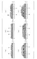
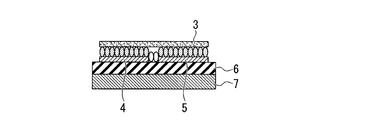
- a top gate type and top contact type organic transistor it is a mimetic diagram in case an organic semiconductor layer is not flat.
- a top gate type top contact type organic transistor it is a mimetic diagram in case an organic semiconductor layer is flat.
- FIG. 2 is a scanning electron micrograph of the surface of the organic semiconductor layer of Example 1.
- FIG. 2 is a scanning electron micrograph of the surface of an organic semiconductor layer of Comparative Example 1.
- 4 is a scanning electron micrograph of the surface of an organic semiconductor layer of Comparative Example 2.
- 2 is a scanning electron micrograph of a cross section of an organic semiconductor layer of Example 1.
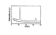
- FIG. 3 is a result of out-of-plane XRD (out-of-plane XRD) measurement of the organic semiconductor layer of Example 1.
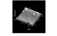
- FIG. 3 is a three-dimensional atomic force micrograph of the surface of an organic semiconductor layer of Example 2.
- 3 is a three-dimensional atomic force microscope photograph of the surface of an organic semiconductor layer of Example 3.
- FIG. 2 is a two-dimensional atomic force microscope photograph of the surface of an organic semiconductor layer of Example 2.
- FIG. 3 is a two-dimensional atomic force microscope photograph of the surface of an organic semiconductor layer of Example 3.
- FIG. 6 is a schematic diagram showing a pattern formed in Example 3.
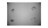
- FIG. 4 is a photograph showing a layer of a solution when the solution is applied in Example 3.
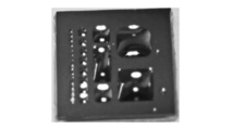
- FIG. 3 is a photograph showing an organic semiconductor layer obtained in Example 3.
- FIG. 6 is an optical micrograph of an organic semiconductor layer of Comparative Example 3.
- 6 is a schematic diagram of an organic transistor obtained in Example 4.
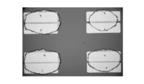
- FIG. 4 is an optical micrograph of an organic transistor of Example 4.
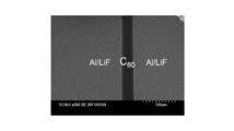
- 4 is a scanning electron micrograph of the surface of an organic transistor of Example 4.
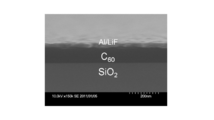
- 4 is a scanning electron micrograph of a cross section of an organic transistor of Example 4.
- FIG. 6 is a top schematic view showing an organic device produced in Example 5.
- FIG. 7 is a schematic cross-sectional view showing an organic device produced in Example 5.
- FIG. 6 is a schematic cross-sectional view of an organic semiconductor layer obtained in Example 6.
- FIG. 10 is a graph showing the transfer characteristics of an organic transistor obtained in Example 7.
- a method for producing an organic semiconductor layer includes preparing a solution by dissolving organic molecules in an organic solvent, applying the solution onto a support, and subjecting the support to a reduced-pressure atmosphere. And drying to form an organic semiconductor layer on the support.
- the manufacturing method of the organic-semiconductor layer in 1 aspect of this invention is demonstrated concretely. Note that the manufacturing method of the organic semiconductor layer in one embodiment of the present invention is not limited to the following specific examples.
- an organic semiconductor layer is formed on a support.
- the organic semiconductor layer 3 is formed on the entire surface of the support made of the substrate 1 having the oxide film 2.
- an organic molecule is dissolved in an organic solvent to prepare a solution (not shown).
- the organic molecule is not particularly limited as long as it can constitute an organic semiconductor, and materials that are usually used for the organic semiconductor layer of an organic transistor can be used.
- the organic semiconductor layer is a p-type semiconductor layer
- pentacene, rubrene, oligothiophene, polythiophene, dinaphthothiophene, or the like can be used
- the organic semiconductor layer is an n-type semiconductor layer.
- C60 fullerene, fluorinated pentacene, peryleneimide compound, or the like can be used.
- the organic molecules in the present embodiment are not limited to those comprising only the molecules constituting the organic semiconductor layer and responsible for the characteristics of the organic semiconductor layer.
- the solvent solubility of the molecules responsible for the characteristics of the organic semiconductor layer is not limited.
- a derivative of a molecule responsible for the characteristics of the organic semiconductor layer may be used as the organic molecule in the present embodiment.
- the electrical characteristics of the organic semiconductor layer may be impaired.
- the molecule constituting the organic semiconductor layer, not the derivative is the organic molecule of this embodiment.
- C60 fullerene is preferable because it has high carrier mobility and can realize high-speed operation of the organic transistor.
- the organic solvent is not particularly limited as long as it can dissolve the organic molecules to be used.
- an organic solvent used for forming an organic semiconductor layer by a solution process using an organic semiconductor material is used. be able to.
- Specific examples include aromatic hydrocarbon solvents such as monochlorobenzene, dichlorobenzene, trichlorobenzene, xylene, and tetralin.
- aromatic hydrocarbon solvents such as monochlorobenzene, dichlorobenzene, trichlorobenzene, xylene, and tetralin.
- trichlorobenzene is preferable as an organic solvent.
- the amount of the organic molecule dissolved in the organic solvent is not particularly limited and can be determined according to the type of the organic solvent and the organic molecule and the solvent temperature at the time of dissolution. It is preferably determined to be a solution. Since the solution is an unsaturated solution, that is, a solution having a relatively low concentration compared to the saturated solution, the solution immediately after being dropped on the substrate may cause aggregation of organic molecules, abnormal crystal growth, or fine crystal grains. It is possible to create a state where formation is difficult to occur. After that, by performing a decompression step, the solvent quickly evaporates, and organic molecules are deposited on the substrate before aggregation of organic molecules and abnormal crystal growth or microcrystal grain formation occur, thereby reducing the film thickness.
- the concentration is preferably about 0.1 to 1% by mass, which is lower than the saturation concentration of 1.5% by mass.
- the method for dissolving the organic molecule in the organic solvent is not particularly limited, and can be performed by a conventional method.
- a method such as rotating a stirrer in an organic solvent, heating the organic solvent, or allowing a solution containing the organic molecule to stand for a certain period of time in a state where the organic solvent and the organic molecule are in contact with each other.
- a solution in which organic molecules are more uniformly dispersed can be obtained.
- the filtration can be performed using a filter having a pore diameter of about 0.1 ⁇ m to 1.0 ⁇ m.
- the support is not particularly limited.
- the organic semiconductor layer is used for an organic transistor, a substrate; a substrate on which a source electrode and a drain electrode are stacked; a gate electrode and a gate insulating layer are stacked in this order.
- Substrate A substrate in which a gate electrode, a gate insulating layer, a source electrode, and a drain electrode are stacked in this order can be given.
- FIG. 1 shows an example in which a substrate 1 having a surface provided with an oxide film 2 is used as a support.
- the surface of the support prepared as shown in FIG. 1A (the substrate 1 provided with the oxide film 2 in FIG. 1A) is preferably cleaned in advance.
- the support can be washed by a conventional method. Specific examples include washing with water, washing with an organic solvent such as acetone, washing with UV-O 3 , and combinations of these washings.
- the method of applying the solution on the support is not particularly limited.
- These methods can be carried out using a known apparatus such as a spin coater or a spray coater.
- coat by discharging a solution to a support body using an inkjet.
- the amount of the solution applied onto the support is not particularly limited, and can be appropriately determined according to the layer thickness required for the organic semiconductor layer to be formed.
- the reduced pressure atmosphere in the present embodiment refers to an atmosphere filled with a gas having a lower pressure than atmospheric pressure.
- the pressure of the atmosphere during drying of the support is not particularly limited as long as it is lower than atmospheric pressure, and can be appropriately determined in consideration of the amount of the solution, the size of the substrate, etc. preferable.
- a high vacuum of 10 ⁇ 5 Pa to 0.1 Pa or a medium vacuum of 0.1 Pa to 100 Pa is preferable.
- the productivity (yield) of the organic semiconductor layer and the carrier mobility of the organic semiconductor layer Is preferable.
- the atmosphere around the support from atmospheric pressure to about 1 Pa to 10 Pa relatively slowly, the time until drying becomes longer, but the flatness of the formed organic semiconductor layer is further improved, which is preferable.
- the method of drying the support in a reduced-pressure atmosphere is not particularly limited.
- the support coated with the solution is allowed to stand in a sealed container equipped with a decompression facility, and the inside of the sealed container is decompressed. And then drying.
- a decompression facility or a sealed container a known decompression drying apparatus including an exhaust pump 11 such as a rotary pump or a mechanical booster pump can be used.
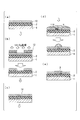
- the organic semiconductor layer made of organic molecules as shown in FIG. can get.
- the organic semiconductor layer thus obtained is uniform and flat, and has improved carrier mobility as well as the deposited film.
- the organic solvent is evaporated in a shorter time than when drying in the air without applying energy such as heat, It is considered that the above-described effects can be obtained without aggregation of organic molecules in the applied solution or abnormal crystal growth or microcrystal grain formation due to organic molecules in the layer even in organic molecules having high crystallinity.
- an organic semiconductor layer can be formed using an organic molecule solution having a relatively low concentration as described above, an organic molecule having low solubility in an organic solvent such as C60 fullerene is used. Even when used, the organic semiconductor layer can be easily produced by a solution process.
- the support has a solvent repellent part and a lyophilic part with respect to the organic solvent, whereby the organic semiconductor layer is formed on the lyophilic part, and is patterned. It will be.
- a solvent-repellent portion made of a 1,1,1,3,3,3-hexamethyldisilazane (HMDS) monomolecular film is formed on the surface of a substrate 1 having an oxide film 2 and trimethoxyphenyl.
- HMDS 1,1,1,3,3,3-hexamethyldisilazane
- the organic semiconductor layer 3 is formed only in a specific region of the support and has a pattern.
- a monomolecular film 12 made of HMDS is formed on a substrate 1 provided with an oxide film 2 (FIG. 2A), and then UV-O is passed through a metal mask 13 having an opening. 3 process is performed and the HMDS film
- TMPS monomolecular film 14 on the surface of the part
- the patterned substrate 1 having the solvent-repellent portion made of the HMDS monomolecular film 14 and the lyosolvent portion made of the TMPS monomolecular film 12 thus formed is used as a support.
- a solution prepared by dissolving organic molecules in an organic solvent is applied on the support (FIG. 2D).
- the applied solution selectively collects on the surface of the TMPS monomolecular film 14 exhibiting solvophilicity in accordance with the wettability (solvophilicity, solvent repellency) of the support surface.
- the support coated with the solution is dried in a reduced-pressure atmosphere, whereby the organic semiconductor layer 3 is formed only on the lyophilic portion, whereby the patterned organic semiconductor layer 3 is manufactured (FIG. 2). (E)).
- the solvent-repellent part and the parent solvent part are formed using HMDS and TMPS, but the method of forming the solvent-repellent part and the parent solvent part in the second embodiment is not limited to this.
- the size and shape of the solvent repellent part and the lyophilic part are not particularly limited, and can be appropriately determined according to the characteristics of the target organic semiconductor layer. For example, in the case of forming an organic semiconductor layer as shown in FIG. 3B described later, it is preferable to form a solvophilic portion having a size corresponding to the channel portion.
- a method of forming the solvent repellent part and the lyophilic solvent part for example, a method of chemically treating the surface of a substrate or the like using a solvent repellant compound and a solvophilic compound as shown in FIG. And a method of physically treating the surface of a substrate or the like using the above method.
- a solvent-repellent compound and a solvophilic compound is preferable because surface treatment can be easily performed.
- the solvent repellent compound and the lyophilic compound are not particularly limited, and can be appropriately determined according to the type of the organic solvent that dissolves the organic molecule. Specifically, when an aromatic hydrocarbon solvent such as trichlorobenzene is used as the organic solvent, an organic molecule having an aromatic group in a part of its structure can be a solvophilic compound. On the other hand, any aliphatic organic molecule having no aromatic group in its structure can be a solvent-repellent compound. Further, the solvophilic compound and the solvent-repellent compound remain in the lower layer of the obtained organic semiconductor layer as constituting a part of the support unless special treatment is performed.
- an aromatic hydrocarbon solvent such as trichlorobenzene
- any aliphatic organic molecule having no aromatic group in its structure can be a solvent-repellent compound.
- the solvophilic compound and the solvent repellent compound those having a property that does not hinder the functions of the organic semiconductor layer and the device to which the organic semiconductor layer is applied are preferable.
- the solvent-repellent part and the lyophilic part are provided on a silicon substrate with a SiO 2 oxide film, the solvent has the same properties as those of the silicon substrate and has Si atoms in its structure. It is preferable to use a compound satisfying the solvent repellency or solvophilicity.
- the solvent-repellent compound is used.
- HMDS octadecyltrichlorosilane, octadecyltrimethoxysilane, perfluoroalkylsilane and the like
- TMPS dimethoxydiphenylsilane, triphenylsilanol, phenethyltrichlorosilane and the like can be preferably used.
- the method for forming the solvent-repellent part and the parent-solvent part using the solvent-repellent compound and the solvophilic compound is not particularly limited, but any of the solvent-repellent compound and the solvophilic compound on the surface of the substrate or the like.
- a thin film is formed using either of these, and after removing a part of the formed thin film by selective irradiation with ultraviolet rays, ozone (O 3 ), etc., either the solvent repellent compound or the solvophilic compound is removed.
- a preferred method is to use and form a thin film made of any one of the other in the removal portion. Either the solvent repellent part or the lyophilic solvent part may be formed first.
- the thin film is not particularly limited, but it is preferably a relatively thin film so as not to impair the properties of the substrate and the like.
- a monomolecular film made of a compound or a solvophilic compound is preferred.
- the method for forming a thin film or monomolecular film is not particularly limited, and is formed by appropriately combining conventional methods such as a solution immersion method, a gas phase reaction method, a spin coating method / dip coating method, and a Langmuir Blodgett method. be able to. Note that the method disclosed in Japanese Patent Application Laid-Open No. 2009-212127 can be applied to the method for forming the patterned organic semiconductor layer.
- a compound capable of specifically binding to the member is added.
- a solvent repellent part and a lyophilic part can also be formed by using as a solvent repellent part forming compound or a lyophilic part forming compound.
- a thiol that specifically binds to gold is used to Appropriate thiols can be selected in view of the dipole moment and wettability to organic solvents.
- the organic solvent is an aromatic hydrocarbon solvent and the carrier is an electron and an n-type semiconductor
- the electric dipole moment is directed to the organic semiconductor layer from the source electrode and the drain electrode.
- it is a material which has an aromatic from a solvophilic viewpoint.
- Specific examples include 4-dimethylaminobenzenethiol, 4-aminobenzenethiol, 4-hydroxybenzenethiol, methylbenzenethiol, and the like.
- the carrier is a hole and is a p-type semiconductor, it is a material in which the direction of the electric dipole moment is directed from the organic semiconductor layer to the source electrode and the drain electrode, and similarly, a material having aromaticity.
- Specific examples include 4-nitrobenzenethiol and perfluorobenzenethiol. Note that this method is useful when a bottom contact type organic transistor is specifically manufactured when it is necessary to form an organic semiconductor layer on the source electrode and the drain electrode.
- the step of preparing the solution in the second embodiment is the same as that in the first embodiment.
- the support is changed so that the solution is concentrated only on the parent solvent part. It is preferable to cause the solution to flow on the support by tilting or the like.
- the step of forming the organic semiconductor layer in the second embodiment is the same as that in the first embodiment.
- an organic semiconductor layer formed in a pattern on the support is obtained.
- Such a patterned organic semiconductor layer is useful, for example, as an organic semiconductor layer constituting an organic transistor.
- FIG. 3A and FIG. 3B show a bottom gate type and top contact type organic material in which a substrate 1, a gate insulating layer 7, a gate electrode 6, an organic semiconductor layer 3, a source electrode 4 and a drain electrode 5 are laminated in this order. The case of a transistor is shown.
- a gate leakage current (arrow in the figure) flows from the source electrode 4 to the gate electrode 7 through the organic semiconductor layer 3. End up.
- the support has a solvent repellent part and a lyophilic part with respect to an organic solvent, and at least a small region of the solvent repellent part has the parent region.
- the organic semiconductor layer is formed on the lyophilic solvent part and on the minute region of the solvent repellent part.
- an organic semiconductor layer is formed by providing a support by providing a solvent repellent portion made of HMDS monomolecular film 12 and a lyosolvent portion made of TMPS 14 on the surface of the substrate 1 having the oxide film 2.
- 3 is formed only in a specific region of the support and has a pattern.
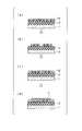
- a monomolecular film 14 made of TMPS is formed on the substrate 1 provided with the oxide film 2 (FIG. 4A), and then part of the TMPS film 14 is removed (FIG. 4). (B)). Thereafter, the surface of the part from which the TMPS film 14 has been removed is reacted with HMDS to form the HMDS monomolecular film 12 on the surface of the part ((c) of FIG. 4).
- the patterned substrate 1 having the solvent-repellent part made of the HMDS monomolecular film 12 and the lyosolvent part made of the TMPS monomolecular film 14 thus formed is used as a support. Use.
- FIG. 4A a monomolecular film 14 made of TMPS
- the support has a plurality of solvent-repellent parts and a plurality of solvent-repellent parts, and a part of the solvent-repellent part (the center part in (c) to (d) of FIG. 4) is It is a minute region surrounded by the lyophilic part.
- a solution prepared by dissolving organic molecules in an organic solvent is applied onto the support, and the support is dried in a reduced-pressure atmosphere, so that the micro solvent on the parent solvent part and the solvent repellent part is obtained.
- a patterned organic semiconductor layer 3 is manufactured (FIG. 4D).
- the fact that at least a part of the minute region of the solvent-repellent part is surrounded by the lyophilic solvent part means that the minute region that is a part or all of the solvent-repellent part is in the solvent part as shown in FIG. It means a state where at least about half of the sides surrounding the minute region are in contact with the lyophilic solvent part.
- an organic semiconductor layer is formed on the lyophilic portion and the microregion by the solvent repellent portion having the microregion as described above. After the solution is applied, the layer of the solution containing organic molecules is normally selectively present only on the parent solvent portion.
- a part of the solvent-repellent part surrounded by the lyophilic solvent part is minute, liquid droplets exist not only on the lyophilic part but also on the minute region.
- an organic-semiconductor layer is also formed on the micro area
- the size and area of the microregion are not particularly limited, and the solvophilicity of the solvophilic part used, the solvent repellency of the solvent repellent part used, the area and arrangement of the lyophilic part and the solvent repellent part, the surface of the organic solvent It can be appropriately determined in consideration of tension and the like.
- region means the area
- the formation method and material of the lyophilic part and the solvent repellent part and the pattern of the formed organic semiconductor layer according to the third embodiment are not limited to those shown in FIG.
- the method for forming the lyophilic portion and the solvent repellent portion in the third embodiment and FIG. 4 the step of preparing the solution, the step of applying the solution on the support, and the step of forming the organic semiconductor layer are the same as above. It is.
- an organic semiconductor layer can be formed not only on the lyophilic part of the support but also on a minute solvent-repellent part surrounded by the lyophilic part. .
- Such an organic semiconductor layer is useful when a partial region of a lower layer (layer having a function as a lyophilic solvent part or a solvent repellent part) in contact with the organic semiconductor layer is preferably solvent repellent for some reason. .
- a partial region of a lower layer layer having a function as a lyophilic solvent part or a solvent repellent part
- a bottom contact transistor described later with reference to FIG. Details of the configuration shown in the figure will be described later.
- an organic semiconductor layer is formed on the source electrode, the drain electrode, and between the source electrode and the drain electrode (the interface between the source electrode and the drain electrode and the gate insulating layer serves as a channel). Form.
- the organic semiconductor layer can be formed on the channel region even if the channel region is the solvent repellent portion.
- the size of the source electrode and the drain electrode is about 1000 ⁇ m long ⁇ about 400 ⁇ m wide, and the region of the channel portion is about 1000 ⁇ m long ⁇ about 5 ⁇ m to 40 ⁇ m wide, and is located in the solvophilic region of the source electrode and the drain electrode.
- the solvent repellent part region of the channel part is sufficiently small.
- the hydroxyl group functions as a carrier trap. Therefore, in order to improve the carrier mobility, it is known to modify the channel region to a hydrophobic surface. If the manufacturing method of the third embodiment is used, it is possible to introduce a solvent-repellent part into the channel region, and the surface of the solvent-repellent part is generally smaller in surface energy and larger in hydrophobicity than the surface of the lyophilic part. Improvement of carrier mobility can be realized.
- an organic semiconductor layer, a source electrode and a drain electrode are formed on a substrate in an arbitrary order, and further, a gate insulating layer and a gate electrode are formed in this order.
- the organic semiconductor layer is formed by dissolving an organic molecule in an organic solvent to prepare a solution, applying the solution on a substrate or a source electrode and a drain electrode, and drying in a reduced pressure atmosphere. Forming a semiconductor layer.
- the organic transistor manufactured according to the fourth embodiment is a top gate type in which the gate electrode is on the gate insulating layer.
- the organic transistor manufactured according to the fourth embodiment has a source on the organic semiconductor layer 3 even if the source electrode 4 and the drain electrode 5 are bottom contact type (FIG. 6A) in which the organic semiconductor layer 3 is formed below.
- the top contact type (FIG. 6B) for forming the electrode 4 and the drain electrode 5 may be used, or other types of organic transistors may be used.
- the organic semiconductor layer 3 is formed, whereby the bottom contact type organic transistor of FIG. 6A can be manufactured.
- the source electrode 4 and the drain electrode 5 are formed, whereby the top contact type organic transistor of FIG. 6B can be manufactured.
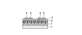
- FIG. 6A is a schematic diagram illustrating a top-gate and bottom-contact organic transistor.
- the source electrode 4 and the drain electrode 5 are formed on the substrate 1.
- the organic semiconductor layer 3 is formed, and the gate insulating layer 6 and the gate electrode 7 are formed in this order, whereby an organic transistor can be manufactured.
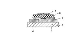
- the top gate type and top contact type organic transistor as shown in FIG. 6B is manufactured by the organic transistor manufacturing method of the fourth embodiment, after the organic semiconductor layer 3 is formed on the substrate 1.
- the organic transistor can be manufactured by forming the source electrode 4 and the drain electrode 5 and further forming the gate insulating layer 6 and the gate electrode 7 in this order.
- substrate 1 What is normally used as a board
- a metal substrate such as aluminum or iron; an inorganic material substrate other than a metal such as silicon, quartz, or glass; an organic resin material substrate such as polycarbonate, polyetheretherketone, polyimide, polyester, or polyethersulfone; Can be mentioned.
- an organic resin material substrate is preferable in consideration of application to a flexible device.
- the substrate 1 may be one in which electrodes such as ITO, gold, silver, copper, platinum, and chromium are formed on the surface, and another thin film is formed on the substrate surface or the electrode surface formed on the substrate. It may be formed.
- Examples of the other thin film include a gate insulating film made of an oxide film such as silicon dioxide (SiO 2 ).
- silicon is used as the substrate, gold is used as the source and drain electrodes, and a bottom contact type organic transistor is manufactured, that is, when the silicon substrate and the gold electrode are in direct contact, the silicon substrate and the gold electrode are generally used.
- an adhesion layer made of chromium, titanium, gold germanium nickel alloy, gold nickel alloy, etc. between the gold and the substrate (gold nickel alloy adhesion) (For example, refer to JP 2010-135542 A).
- the source electrode 4 and the drain electrode 5 are not particularly limited, and those usually used for these electrodes of a transistor can be used. Specifically, for example, gold (Au), silver (Ag), copper (Cu), platinum (Pt), palladium (Pd), iron (Fe), aluminum (Al), tantalum (Ta), chromium (Cr) Metal materials such as indium tin oxide (ITO), zinc oxide (ZnO), tin oxide (SnO 2 ) and other oxide conductors; transparent conductive material composed of indium oxide and zinc oxide, which are a kind of oxide conductors Etc. Further, an electrode made of an organic material such as polyaniline or polythiophene, or an electrode formed by applying a conductive ink can also be used.
- the organic semiconductor layer 3 is the same as described above.
- the method for forming the organic semiconductor layer 3 on the substrate 1 or on the source electrode 4 and the drain electrode 5 is the same as the method for manufacturing the organic semiconductor layer of the first embodiment.
- the “support” in the first embodiment is the substrate 1 or the substrate 1, the source electrode 4, and the drain electrode 5.
- the method of forming the source electrode 4 and the drain electrode 5 on the substrate 1 or the organic semiconductor layer 3 is not particularly limited. Specifically, for example, vacuum deposition or the like on the organic semiconductor layer via a mask is performed.
- the source electrode 4 and the drain electrode 5 can be formed by lithography.
- the gate insulating layer 6 is not particularly limited, and a material usually used for a gate insulating layer of a transistor can be used. Specifically, for example, inorganic oxides such as silicon dioxide (SiO 2 ), aluminum oxide (Al 2 O 3 ), and tantalum oxide (Ta 2 O 5 ); polyimide, polyethylene, polyethylene naphthalate, polyvinylphenol and the like And polymer materials.
- the gate insulating film may be a stacked layer of a silicon dioxide (SiO 2 ) film and any one of a Cytop layer, an HMDS layer, a TMPS layer, and a CYCLOTENE layer. Examples of the gate electrode 7 include those similar to the source electrode 4 and the drain electrode 5 described above.
- the method for forming the gate insulating layer 6 and the gate electrode 7 on the organic semiconductor layer 3 or on the source electrode 4 and the drain electrode 5 is not particularly limited, and specifically, for example, sputtering through a mask. After forming the gate insulating layer 6 by sputtering, the gate insulating layer 6 and the gate electrode 7 can be formed by sputtering the material of the gate electrode 7 from above.
- the organic semiconductor layer 3 is formed in the same manner as in the first embodiment, so that the organic semiconductor layer 3 constituting the organic transistor is uniform and flat and is deposited.
- the carrier mobility is improved as in the case of the film.
- the transistor characteristics of the organic transistor are excellent.
- the surface of the organic semiconductor layer 3 is flat, for example, a transistor exhibiting excellent characteristics when a top contact transistor is manufactured.
- a source electrode 4 and a drain electrode 5 are formed in an upper layer of the organic semiconductor layer 3, and a gap between these electrodes is formed.
- the manufacturing method of the organic transistor of 4th embodiment formation of the organic-semiconductor layer 3 can be performed similarly to said 2nd embodiment or 3rd embodiment.
- the patterning promoting layer before forming the organic semiconductor layer, the patterning promoting layer having a solvent repellent part and a lyophilic part for the organic solvent used for forming the organic semiconductor layer Forming.
- the patterning promoting layer has a solvent repellent part and a lyophilic part, and the formation thereof is the same as the method for forming the lyophilic part and the solvent repellent part of the second and third embodiments.
- the materials of the solvent repellent part and the lyophilic solvent part are the same as those shown in the second and third embodiments.
- the resulting organic semiconductor layer 3 is patterned by the patterning promoting layer located below the organic semiconductor layer 3. Can be used.
- the organic semiconductor layer 3 can be formed.
- the pattern of the organic semiconductor layer 3 may be a pattern in which the organic semiconductor layer 3 is formed only on the lyophilic portion of the patterning promoting layer as shown in the second embodiment.
- FIG. 8 shows a method of manufacturing a bottom contact type organic transistor having a patterning promoting layer.
- the example of FIG. 8 is an example in which the organic semiconductor layer 3 is formed on the solvophilic portion of the patterning promoting layer and on the minute solvent-repellent portion surrounded by the solvophilic portion.
- a substrate 1 provided with an oxide film 2, a source electrode 4 and a drain electrode 5 is prepared (FIG. 8A), and a monomolecular film 12 made of HMDS is formed on a part of the substrate 1. (FIG. 8B), the surface of the part where the HMDS film 12 is not formed and TMPS are reacted to form a TMPS monomolecular film 14 on the surface of the part (FIG.
- the HMDS monomolecular film 12 as the solvent repellent part and the TMPS monomolecular film 14 as the lyophilic part constitute a patterning promoting layer.
- a patterned organic semiconductor layer 3 is formed on the lyophilic portion and the minute regions of the solvent-repellent portion ((e) of FIG. 8).
- an organic transistor is manufactured by forming the gate insulating layer 6 and the gate electrode 7 ((f) of FIG. 8).
- the compound which forms a solvent repellent part and a lyophilic part is not limited to HMDS and TMPS in FIG.
- the gate leakage current can be reduced and the transistor characteristics can be improved as in the second and third embodiments.
- the method of manufacturing the organic transistor of the fourth embodiment having the patterning promoting layer shown in FIG. 8 as in the third embodiment, not only the solvophilic part but also the solvent part is surrounded.
- the organic semiconductor layer 3 can also be formed on the fine solvent-repellent portion. Therefore, in the bottom contact transistor, an organic semiconductor layer can be selectively formed on the source electrode 4, the drain electrode 5, and the channel, and the channel can be made to have solvent repellency. Can be made particularly excellent in the transformer characteristics.
- a gate electrode and a gate insulating layer are formed on a substrate so as to cover at least part of the gate electrode, and the organic semiconductor overlaps with the gate electrode and the gate insulating layer.
- Forming the layer and the source electrode and the drain electrode in any order, and forming the organic semiconductor layer comprises dissolving an organic molecule in an organic solvent to produce a solution, and the solution is formed on the gate insulating layer. Alternatively, it may be applied on the source electrode and the drain electrode and dried in a reduced pressure atmosphere to form an organic semiconductor layer.
- the organic transistor manufactured according to the fifth embodiment is a bottom gate type in which the gate electrode is on the substrate. Further, the organic transistor manufactured according to the fifth embodiment is a bottom contact type in which the source electrode and the drain electrode are formed below the organic semiconductor layer, but the top in which the source electrode and the drain electrode are formed on the organic semiconductor layer. It may be a contact type or another type of organic transistor.
- a bottom contact type organic transistor can be manufactured by forming an organic semiconductor layer after forming a source electrode and a drain electrode on a gate insulating layer.
- a top contact type organic transistor can be manufactured by forming a source electrode and a drain electrode after forming an organic semiconductor layer on a gate insulating layer.
- the substrate, the gate electrode, the gate insulating layer, the organic semiconductor layer, the source electrode and the drain electrode, and the manufacturing method thereof in the fifth embodiment are the same as those in the fourth embodiment.
- the organic transistor manufacturing method according to the fifth embodiment includes a solvent repellent part and a lyophilic part for an organic solvent used for forming the organic semiconductor layer before the organic semiconductor layer is formed. Forming an organic semiconductor layer in a pattern.
- the patterning promoting layer, the formation method thereof, and the pattern of the obtained organic semiconductor layer are the same as those in the fourth embodiment.
- an organic semiconductor layer that is uniform in yield and improved in carrier mobility can be obtained, so that the obtained organic transistor has excellent transistor characteristics.
- the gate leakage current can be reduced as described above, and the transistor characteristics can be improved.
- the transistor characteristics of the obtained organic transistor are particularly excellent. Can be.
- the organic transistor of the sixth embodiment is obtained by the method for manufacturing the organic transistor of the fourth or fifth embodiment, and is the same as the organic transistor described in the fourth or fifth embodiment.
- the characteristic evaluation of the organic transistor of this embodiment can be performed using a known method. Specifically, when the channel length is about 40 ⁇ m to 200 ⁇ m, about 30 V is applied between the source and drain, and when the gate insulating layer is about 300 nm, the gate voltage is about ⁇ 5 V to 30 V. By plotting the current value between the source and drain, it can be confirmed that the organic transistor satisfies general transistor requirements.
- the display device of the seventh embodiment includes the organic transistor obtained in the sixth embodiment, and a display layer electrically connected to the organic transistor and made of liquid crystal, organic electroluminescence, or electrophoresis.
- FIG. 9A shows a cross-sectional view of the display element of this embodiment when a liquid crystal display layer is provided.
- the drain electrode 22 of the organic transistor 21 of the sixth embodiment is electrically connected to the pixel electrode 25, and the display device includes a counter electrode 26 and a counter substrate 28 facing the pixel electrode 25. . Further, a display layer 27 is provided between the pixel electrode 25 and the counter electrode 26.
- the gate electrode 23 of each organic transistor 21 is electrically connected to the gate bus line 30, and the source electrode 24 is electrically connected to the source bus line 29. Further, the gate bus line 30 is connected to a scanning line driver 32 for sending an electric signal. The source bus line 29 is connected to a video signal driver 33 for sending a video signal.
- the controller 34 controls the operations of the scanning line driver 32 and the video signal driver 33 based on the CPU 35.
- the power supply circuit 36 supplies power to the scanning line driver 32 and the video signal driver 33.
- the display device of the seventh embodiment can have the same configuration as the conventional display device except that the organic transistor of the fourth or fifth embodiment is used, and includes a circuit board, liquid crystal, organic electroluminescence, and electricity. Electrophoretic pixels and drivers are not particularly limited, and known and commonly used ones can be used.
- Example 1 In the same manner as in the first embodiment, an organic semiconductor layer was manufactured by the manufacturing method shown in the schematic diagram of FIG. As Example 1, first, a silicon substrate on which a 300 nm-thick thermal silicon oxide film (SiO 2 ) is formed is prepared as a support for forming an organic semiconductor layer, and organic solvent cleaning with acetone, pure water cleaning, and UV are performed. The support was washed with a combination of -O 3 washing.
- a solution for forming an organic semiconductor layer on the support was prepared. Specifically, 0.5 mass% C60 fullerene was added to trichlorobenzene, which is an aromatic hydrocarbon solvent, and allowed to stand at room temperature for 24 hours to dissolve C60 fullerene, and then a filter having a pore size of 0.2 ⁇ m was used. Then, the C60 fullerene solution containing no solid component was prepared by removing the solid component C60 fullerene that was not completely dissolved. Subsequently, the solution was taken in a syringe or the like, and a predetermined amount was dropped onto the support to form a solution layer on the support.
- trichlorobenzene which is an aromatic hydrocarbon solvent
- the support on which the solution layer was formed was placed in a vacuum container, the gas in the container was evacuated using a rotary pump, and the pressure in the container was reduced to 5 Pa without controlling the temperature in the container.
- a stainless steel pressure vessel having a volume of 1 L was used as the decompression vessel, and RV12 (manufactured by Edwards) was used as the rotary pump. It took about 10 seconds to reach a pressure of 3 kPa or less.
- the support was left in the container, and the organic solvent was desorbed from the solution layer and dried for about 10 minutes to produce an organic semiconductor layer made of C60 fullerene as a solute on the support. .
- Example 2 C60 fullerene was vapor-deposited on the same support as in Example 1, and an organic semiconductor layer made of C60 fullerene was produced on the support.
- the degree of vacuum at this time was 10 ⁇ 5 Pa, the deposition rate was 0.02 nm / s, and the film thickness was 60 nm.
- Example 1 (Observation with surface scanning electron microscope) The surface of the obtained organic semiconductor layer was observed with a scanning electron microscope (SEM).
- SEM scanning electron microscope
- Example 1 As shown in FIG. 10, a uniform organic semiconductor layer was formed. In addition, although a lump portion of about several tens of nm was observed partially, a uniform and flat thin film was formed between these lumpes.
- Comparative Example 1 As shown in FIG. 11, a plate-like single crystal having a thickness of about 1.5 ⁇ m was observed, and it was found that the C60 fullerene was a crystallized flake.
- Comparative Example 2 as shown in FIG.
- the organic semiconductor layer of Example 1 had no periodic structure showing crystallinity in the film thickness direction. From the cross-sectional scanning electron microscope image shown in FIG. 13 and the result of out-of-plane XRD shown in FIG. 14, the organic semiconductor layer of Example 1 has a grain boundary (crystal grain boundary). In addition, since there was no periodic structure showing crystallinity in the film thickness direction, it was confirmed that the film was amorphous, not single crystal or polycrystalline.
- Example 2 The uniformity and flatness of the organic semiconductor layer due to the difference in the pressure reduction rate during the production of the organic semiconductor layer were examined.
- An organic semiconductor layer was manufactured in the same manner as in Example 1 except that a stainless steel pressure vessel having a volume of about 72 L was used as the decompression vessel and the exhaust speed was reduced. In this example, it took about 1 minute to reach 3 kPa or less. After completion of the depressurization, the support was left in the container, and the organic solvent was desorbed from the solution layer and dried for about 10 minutes to produce an organic semiconductor layer made of C60 fullerene as a solute on the support. .
- Example 1 (Observation with atomic force microscope) The organic semiconductor layers obtained in Examples 1 and 2 were observed using an atomic force microscope (AFM).
- the flatness was high.
- the carrier mobility of the organic semiconductor layer of this example which will be described later, is about four times higher than the carrier mobility of Non-Patent Document 1. That is, according to the manufacturing method of this example, an organic semiconductor layer having both high flatness and high carrier mobility can be obtained.
- Example 3 The formation of the organic semiconductor layer when the solvent repellent part and the lyophilic part were formed on the support was examined.
- a 300 nm silicon substrate with a SiO 2 film (14 mm ⁇ 14 mm) that was cleaned in the same manner as in Example 1 was prepared, and the surface of the SiO 2 film of the silicon substrate was repellent with respect to an aromatic hydrocarbon solvent.
- a monomolecular film made of HMDS exhibiting properties was formed. Specifically, HMDS and a substrate are placed in a sealed container, and a monomolecular film made of HMDS bonded to the SiO 2 surface is formed on the substrate by placing the substrate in an atmosphere of 120 ° C. for 10 minutes and exposing the substrate to HMDS vapor. did.
- a metal mask having an opening was placed on the substrate on which the HMDS monomolecular film was formed, and the surface on the metal mask side was treated with UV-O 3 to remove HMDS molecules in the metal mask opening.
- a metal mask shown in FIG. 19 capable of forming a target pattern was used.
- the square pattern 32 formed from the TMPS portion in FIG. 19 is 4 mm square, 2 mm square, 1 mm square, and 0.5 mm square from the right.
- the portion other than the TMPS portion is a region 31 where the HMDS portion is formed.
- TMPS showing solvophilicity with respect to the aromatic hydrocarbon solvent on the surface of the SiO 2 film from which HMDS has been removed
- the substrate and TMPS are placed in a sealed container.
- a monomolecular film made of TMPS chemically bonded to the SiO 2 film surface was produced in the region where the HMDS was removed by treatment at 120 ° C. for 45 minutes.
- TMPS does not come into contact with the SiO 2 film surface of the substrate and chemically bond.
- a patterned region of the HMDS surface showing liquid repellency with respect to the aromatic hydrocarbon solvent and the TMPS surface showing solvophilicity was formed on the surface of the SiO 2 film on the substrate.
- a C60 solution using trichlorobenzene as a solvent was dropped on a substrate modified with TMPS / HMDS molecules using a syringe in a similar manner as in Example 1 to form a solution layer on the substrate. .
- the solution on the substrate is selectively collected on the surface of the TMPS molecule treated with TMPS / HMDS molecules and exhibiting solvophilicity due to the difference in solvent wettability.
- Example 3 after dropping C60 droplets on the substrate, the substrate surface is tilted to cause the solution on the substrate surface to flow, and as shown in the photograph of FIG. 20, selectively onto the substrate surface modified by TMPS. A layer of solution was formed.
- a substrate having a C60 fullerene solution layer selectively formed on the TMPS region of the substrate surface was introduced into a vacuum container as in Example 1, and the gas in the container was evacuated to reduce the pressure to about 5 Pa at room temperature. Thereafter, drying was performed for about 10 minutes. A photograph of the substrate after drying is shown in FIG. It was confirmed that an organic semiconductor layer composed of C60 was selectively formed in the region where the solution layer was formed.
- FIG. 22 shows the substrate surface of the organic semiconductor layer produced by the method of Comparative Example 3. As shown in FIG. 22, C60 fullerene aggregates were deposited in a local region, and a uniform and flat organic semiconductor layer as obtained in Example 3 could not be obtained. That is, a uniform and flat organic semiconductor thin film can be obtained by performing a pressure reduction step after applying the solution.
- Example 4 an organic transistor as shown in FIG. 23 was manufactured by forming the source electrode 4 and the drain electrode 5 on the organic semiconductor layer 3 of Example 3 above. Note that the silicon substrate and SiO 2 of the support in Example 3 were used for the lower layer of the gate electrode 7 and the gate insulating layer 6 made of SiO 2 in this example. In the organic transistor of this example, the organic semiconductor layer 3 made of C60 was formed using the method of Example 3 above.
- Al / LiF is deposited on the organic semiconductor layer 3 as a source electrode 4 and a drain electrode 5, and LiF is deposited to a thickness of 1 nm at a thickness of 0.02 nm / s in an atmosphere having a degree of vacuum of about 10 ⁇ 4 through a metal mask.
- Al was deposited at a thickness of 60 nm with a thickness of 0.2 to 0.4 nm / s.
- An optical micrograph of the obtained organic transistor is shown in FIG. In FIG. 24, an oval region surrounded by a line is an organic semiconductor layer (vertical 1 mm ⁇ width 2 mm; thickness 60 nm) made of C60 fullerene. It was confirmed that the two rectangular regions overlapping the elliptical region in FIG.
- the scanning electron beam microscope image of the surface of the obtained organic transistor is shown in FIG. As shown in FIG. 25, it was confirmed that the surface of the obtained organic transistor had no grain boundary like the scanning electron microscope image of the deposited film shown in FIG. Furthermore, in the scanning electron microscope image of the cross section of the organic transistor shown in FIG. 26, the interface between C60 and Al / LiF is less uneven, and the organic semiconductor layer is highly flat even after the source and drain electrodes are formed. It was confirmed that the sex was maintained.
- FIG. 28 shows the result of plotting the current value between the source and drain when 10 V, 20 V, or 30 V is applied between the source and drain and the drain voltage is applied from 0 to 30 V.
- FIG. 29A is a schematic top view.
- FIG. 29B is a schematic sectional view taken along the arrow in FIG. 29A.
- patterning of the source electrode 4 and the drain electrode 5 was performed using gold on the substrate 1 made of silicon and SiO 2 having the gate electrode 7 and the gate insulating layer 6 by photolithography. .
- the pattern of the source electrode 4 and the drain electrode 5 is 1.0 mm ⁇ 0.4 mm, and the distance (channel length) between the electrodes is 5 ⁇ m to 40 ⁇ m.
- the silicon substrate 1 provided with the source electrode 4, the drain electrode 5, the gate insulating film 6 made of SiO 2 , the gate electrode 7, and the oxide film was subjected to HMDS treatment in the same manner as in Example 4. Since HMDS does not react with gold, a solvent-repellent portion is selectively formed only in a portion where the gate insulating film 6 (SiO 2 film) on the silicon substrate 1 is exposed. Next, a solvophilic portion was selectively formed only on the source electrode 4 and the drain electrode 5 using 4-dimethylaminobenzenethiol, which is a molecule having a thiol group that selectively reacts with gold.
- Example 1 Thereafter, a 0.5 mass% trichlorobenzene solution of C60 fullerene obtained in the same manner as in Example 1 was applied.
- the applied solution tends to accumulate selectively on the source electrode 4 and the drain electrode 5 as in the case of Example 4 described above, but the channel length is very large compared to the area of the source electrode 4 and the drain electrode 5. Since it is short, the solution also covers the channel which is the solvent repellent part, and as a result, the entire source electrode 4 and drain electrode 5 are covered with one solution layer.
- the substrate 1 covered with the solution layer was dried under reduced pressure in the same manner as in Example 1. As a result, the solution dried rapidly, and a uniform thin film was formed on the solvent-repellent surface (channel portion). . That is, since a solvent-repellent surface can be introduced into the channel portion, carrier mobility can be improved.
- Example 6 In this example, an organic semiconductor layer made of C60 fullerene was formed, and the relationship between the wettability of the support surface, the exhaust speed when the organic semiconductor layer was dried under reduced pressure, and the yield of film formation was evaluated.
- a silicon substrate (hereinafter also referred to as a substrate) on which a thermal silicon oxide film (SiO 2 film) 6 having a thickness of 35 nm was formed was prepared as the support 1 for forming the organic semiconductor layer 3.
- a layer (underlayer) 8 having different wettability with respect to the aromatic hydrocarbon solvent was formed.
- a Cytop layer, an HMDS layer, a TMPS layer, and a CYCLOTENE layer were used.
- the organic semiconductor layer 3 was formed on the base layer 8. The substrate was cleaned by the same method as in Example 1.
- the Cytop layer was formed by diluting a commercially available Cytop stock solution with a dedicated solvent, applying about 65 ⁇ l of the obtained diluted solution on the substrate 1, and spin-coating at 500 rpm for 5 seconds and then at 3000 rpm for 40 seconds. Further, the substrate on which the Cytop layer was formed was heated at 100 ° C. for 30 minutes and then at 250 ° C. for 1 hour.
- the CYCLOTENE layer was diluted by mixing a commercially available CYCLOTENE stock solution in a dedicated solvent T1100 at a mass ratio of 1: 9. About 65 ⁇ l of the obtained diluted solution was applied onto a substrate, and spin-coated at 500 rpm for 5 seconds and then at 3000 rpm for 40 seconds to form a film.
- the substrate on which the CYCLOTENE layer was formed was heated at 100 ° C. for 30 minutes and then at 250 ° C. for 1 hour.
- HMDS layer HMDS and a substrate were placed in a sealed container, placed in an atmosphere of 120 ° C. for 10 minutes, and the substrate was exposed to HMDS vapor to form a HMDS monomolecular film bonded to the surface of the SiO 2 film 6.
- TMPS layer TMPS and the substrate were put in a sealed container, placed in an atmosphere of 120 ° C. for 10 minutes, and the substrate was exposed to TMPS vapor to form a TMPS monomolecular film bonded to the surface of the SiO 2 film 6.
- a static contact angle of a 0.5 wt% C60 trichlorobenzene solution was measured.
- the contact angles of each Cytop layer, HMDS layer, TMPS layer, and CYCLOTENE layer were 66 °, 49 °, 16 °, and 10 °, respectively.
- a C60 fullerene solution was prepared in the same manner as in Example 1. This C60 fullerene solution was filled in an ink jet machine, and discharged at 15 locations on the underlayer 8 at an interval of about 1.6 mm with a discharge amount of 60 nl.
- the substrate 1 coated with the C60 fullerene solution was dried under reduced pressure using the same stainless steel pressure resistant container and rotary pump as in the example.
- the exhaust speed at the time of drying under reduced pressure was controlled by adjusting the degree of opening and closing of the pressure reducing valve as the speed in the time from reaching atmospheric pressure to 10 Pa.
- the formed organic semiconductor layer 3 was observed with an optical microscope, and those having a good thin film as shown in FIG. 21 were counted. Thus, the yield was calculated when the organic semiconductor layer 3 formed on each Cytop layer, HMDS layer, TMPS layer, and CYCLOTENE layer was decompressed at each exhaust speed.
- FIG. 31 shows the relationship between the deposition yield of the organic semiconductor layer 3, the wettability of the surface of each Cytop layer, HMDS layer, TMPS layer, and CYCLOTENE layer, and the vacuum rate of vacuum drying.
- the contact angle is, for example, 50 ° or less, even when the time to reach 10 Pa is about 10 seconds, for example, when the exhaust speed is high, the yield reaches 100%. It was.
- the organic semiconductor layer 3 can be formed with a high yield of 70% or more even when the exhaust speed is low if the contact angle is 16 ° or less and the wettability is good. In other words, it was found that the organic semiconductor layer can be formed with a high yield even under conditions using a pump having a low ultimate vacuum and poor performance.
- the organic semiconductor layer can be formed at a high yield by increasing the exhaust speed, for example, the time to reach 10 Pa is approximately 10 seconds. I found it possible.
- the organic semiconductor layer 3 can be formed with a high yield by appropriately controlling the wettability of the surface of the base layer 8 formed on the substrate 1 and the exhaust speed at the time of drying under reduced pressure.
- Example 7 the organic transistor shown in FIG. 32 was produced.
- a silicon substrate was used as the gate electrode, and a silicon oxide film (SiO 2 film) and a CYCLOTENE layer were formed on the silicon substrate.
- the SiO 2 film and the CYCLOTENE layer are gate insulating films.
- Example 6 Using the same method as in Example 6, a C60 fullerene solution was ejected at 10 locations on the CYCLOTENE layer by an inkjet method and dried under reduced pressure to form an organic semiconductor layer 3 made of C60 fullerene.
- the exhaust speed at the time of drying under reduced pressure required 30 seconds to 80 seconds to reach 10 Pa from atmospheric pressure.
- the silicon substrate on which the organic semiconductor layer was formed was heated on a hot plate at 140 ° C. for 10 minutes to remove a part of the remaining solvent.
- Al was deposited as a source electrode 4 and a drain electrode 5 through a metal mask in an atmosphere with a degree of vacuum of about 10 ⁇ 4 Pa at a rate of 1 ⁇ m / sec to a thickness of 60 nm.
- the silicon substrate on which the source electrode 4 and the drain electrode 5 were formed was heated on a hot plate at 140 ° C. for 10 minutes to remove most of the remaining solvent. As a result, 10 organic transistors were completed on the same substrate.
- the transistor characteristics of 10 organic transistors were evaluated in the same manner as in Example 4. As a result, as shown in FIG. 33, the organic transistor of this example shows good n-type transistor characteristics, and its mobility is 2.4 cm 2 / Vs at the maximum, which is higher than that of Example 4. Indicated.
- the average mobility of the 10 organic transistors obtained in this example was 2.2 cm 2 / Vs, and the average error was ⁇ 0.15 cm 2 / Vs.
- the average threshold voltage was 0.52V, and the average error was ⁇ 0.1V, indicating a small variation.
- the method for producing an organic thin film according to an aspect of the present invention can be suitably used in the field of organic device production.
Landscapes
- Engineering & Computer Science (AREA)
- Manufacturing & Machinery (AREA)
- Chemical & Material Sciences (AREA)
- Nanotechnology (AREA)
- Physics & Mathematics (AREA)
- Mathematical Physics (AREA)
- Theoretical Computer Science (AREA)
- Crystallography & Structural Chemistry (AREA)
- Thin Film Transistor (AREA)
Abstract
有機半導体層の製造方法は、有機分子を有機溶媒に溶解して溶液を作製することと、前記溶液を、支持体上に塗布することと、前記支持体上の前記溶液を減圧雰囲気下で乾燥し、前記支持体上に有機半導体層を形成することを含む。
Description
本発明は、有機分子からなる有機半導体層の製造方法、前記有機半導体層を備えた有機トランジスタの製造方法、前記製造方法により得られる有機トランジスタ、及び前記有機トランジスタを用いた表示装置に関する。
本願は、2011年3月7日に、日本に出願された特願2011-049662号に基づき優先権を主張し、その内容をここに援用する。
本願は、2011年3月7日に、日本に出願された特願2011-049662号に基づき優先権を主張し、その内容をここに援用する。
有機半導体層を備える有機トランジスタは、シリコン等の無機半導体デバイスの作製において、一般的に用いられる真空プロセスや、200℃以上の高温プロセスを用いることなく、インクジェット法やスクリーン法などの印刷技術やスピンコート法、キャスト法等の溶液プロセスを用いて素子作製が可能である。そのため、大面積基板上や、プラスチック等からなるフレキシブル基板上に素子作製が可能である。更に、有機トランジスタは、デバイス作製における製造コストや環境負荷の低減が可能であることから近年注目されている。
通常、有機半導体層は、真空蒸着法や溶液プロセスにより製造されている。真空蒸着法の場合、作製する基板サイズに応じたサイズの真空機器が必要であるため、設備の制約により基板の大型化が困難である。そこで、大型基板にも有機半導体層が簡便に作製可能な、溶液プロセスによる有機半導体層の製造が望まれている。
通常、有機半導体層は、真空蒸着法や溶液プロセスにより製造されている。真空蒸着法の場合、作製する基板サイズに応じたサイズの真空機器が必要であるため、設備の制約により基板の大型化が困難である。そこで、大型基板にも有機半導体層が簡便に作製可能な、溶液プロセスによる有機半導体層の製造が望まれている。
近年では、C60フラーレンからなる有機半導体層を用いて電界効果トランジスタとした場合に高いキャリア移動度が得られることから、C60に代表されるフラーレンは、n型の有機半導体材料として期待されている。
しかしながら、フラーレンは各種溶媒に対する溶解性が低いことから、通常の溶液プロセスによる塗布膜形成が困難である。最近では、単純なスピンコート法により、C60フラーレンを用いた溶液プロセスによる有機トランジスタの製造が試みられている(例えば非特許文献1参照)。
しかしながら、フラーレンは各種溶媒に対する溶解性が低いことから、通常の溶液プロセスによる塗布膜形成が困難である。最近では、単純なスピンコート法により、C60フラーレンを用いた溶液プロセスによる有機トランジスタの製造が試みられている(例えば非特許文献1参照)。
Sungら、「Flexible Fullerene Field-Effect Transistors Fabricated Through Solution Processing」、Advanced Materials、第47巻、第21号、4845~4849頁、2009年12月。
しかしながら、上記非特許文献1記載の方法により、溶液プロセスでC60フラーレンからなる有機半導体層を形成した場合、そのキャリア移動度は0.21cm2/Vs程度と、真空蒸着法によりC60フラーレン半導体層を形成した場合のキャリア移動度(0.4~3.2cm2/Vs程度)よりも低く、トランジスタ特性に劣る。
本発明の態様は上記事情に鑑みてなされたものであって、溶液プロセスを用いて、キャリア移動度に優れた有機半導体層を製造する方法、前記有機半導体層を備えた有機トランジスタを製造する方法、前記製造方法により得られる有機トランジスタ、及び前記有機トランジスタを用いた表示装置を提供することを目的とする。
本発明の態様は上記事情に鑑みてなされたものであって、溶液プロセスを用いて、キャリア移動度に優れた有機半導体層を製造する方法、前記有機半導体層を備えた有機トランジスタを製造する方法、前記製造方法により得られる有機トランジスタ、及び前記有機トランジスタを用いた表示装置を提供することを目的とする。
本発明者らは、上記課題を解決すべく鋭意研究した結果、有機分子を有機溶媒に溶解して塗布した後、減圧雰囲気下で乾燥することにより、層中における有機分子の凝集や異常な結晶成長が抑制され、均一且つ平坦な層が形成される結果、キャリア移動度の向上した有機半導体層が得られることを見出した。
すなわち、本発明の態様は以下の有機半導体層の製造方法、有機トランジスタの製造方法、有機トランジスタ、及び表示装置を提供するものである。
すなわち、本発明の態様は以下の有機半導体層の製造方法、有機トランジスタの製造方法、有機トランジスタ、及び表示装置を提供するものである。
(1)本発明の一態様における有機導体層の製造方法は、有機分子を有機溶媒に溶解して溶液を作製することと、前記溶液を、支持体上に塗布することと、前記支持体上の前記溶液を減圧雰囲気下で乾燥することと、前記支持体上に有機半導体層を形成すること、を含む。
(2)本発明の一態様における有機導体層の製造方法において、さらに、前記支持体の表面上に、前記有機溶媒に対する親溶媒部を形成することを有し、前記溶液を支持体上に塗布することは、前記親溶媒部上に前記溶液を塗布することを含んでいてもよい。
(3)本発明の一態様における有機導体層の製造方法において、前記有機分子がフラーレンであり、前記有機溶媒が芳香族炭化水素系溶剤であってもよい。(4)本発明の一態様における有機導体層の製造方法は、さらに前記支持体に前記有機溶媒に対する撥溶媒部と親溶媒部とを形成することを含み、前記有機半導体層が少なくとも前記親溶媒部上に形成され、前記有機半導体層がパターン状となるよう形成されてもよい。
(4)本発明の一態様における有機導体層の製造方法において、前記支持体に、前記有機溶媒に対する撥溶媒部と親溶媒部とを形成することを含み、前記撥溶媒部の少なくとも一部の微小領域が前記親溶媒部に囲まれており、前記有機半導体層が前記親溶媒部上と、前記微小領域上とに形成されてもよい。
(5)本発明の一態様における有機導体層の製造方法において、前記撥溶媒部が、撥溶媒性の有機単分子膜からなり、前記親溶媒部が、親溶媒性の有機単分子膜からなっていてもよい。
(6)本発明の一態様における有機導体層の製造方法は、さらに前記支持体及び前記有機半導体層を加熱することを含んでいてもよい。
(7)本発明の他の態様における有機トランジスタの製造方法は、基板上に、ゲート電極と、ゲート絶縁層と、有機半導体層と、前記有機半導体層と電気的に接続されたソース電極及びドレイン電極とを形成することを含み、前記有機半導体層の形成は、有機分子を有機溶媒に溶解して溶液を作製することと、 前記有機半導体層が形成される表面に、前記有機溶媒に対する親溶媒部を形成することと、前記溶液を少なくとも前記親溶媒部に塗布することと、減圧雰囲気下で乾燥し、有機半導体層を形成することと、を含む。
(8)本発明の他の態様における有機トランジスタの製造方法において、前記基板上に、前記ゲート電極と、前記ゲート絶縁層と、前記有機半導体層と、前記ソース電極及び前記ドレイン電極と形成することは、前記基板上に前記ゲート電極を形成することと、前記ゲート電極の少なくとも一部を覆うように前記ゲート絶縁層を形成することと、前記ゲート電極および前記ゲート絶縁層に重畳して前記有機半導体層を形成すること、を含んでいてもよい。
(9)本発明の他の態様における有機トランジスタの製造方法において、前記基板上に、前記ゲート電極と、前記ゲート絶縁層と、前記有機半導体層と、前記ソース電極及び前記ドレイン電極と形成することは、前記基板上に前記有機半導体層を形成することと、前記前記有機半導体層の少なくとも一部を覆って前記ゲート絶縁層を形成することと、前記前記有機半導体層および前記ゲート絶縁層に重畳して前記ゲート電極を形成すること、を含んでいてもよい。
(10)本発明の他の態様における有機トランジスタの製造方法は、基板上に、ゲート電極とゲート絶縁層とをこの順番で形成することと、さらに、有機半導体層と、ソース電極及びドレイン電極とを任意の順番で形成することを含み、前記有機半導体層の形成は、有機分子を有機溶媒に溶解して溶液を作製することと、前記溶液を、前記ゲート絶縁層上に、又は、前記ソース電極及び前記ドレイン電極上に塗布することと、減圧雰囲気下で乾燥し、有機半導体層を形成することと、を含む。
(11)本発明の他の態様における有機トランジスタの製造方法において、前記有機分子がフラーレンであり、前記有機溶媒が芳香族炭化水素系溶剤であってもよい。
(12)本発明の他の態様における有機トランジスタの製造方法は、さらに、有機半導体層を形成する前に、前記有機溶媒に対する撥溶媒部と親溶媒部とを有するパターン化促進層を形成することを含み、前記有機半導体層が少なくとも前記親溶媒部上に形成され、前記有機半導体層がパターン状となってもよい。
(13)本発明の他の態様における有機トランジスタの製造方法において、さらに、有機半導体層を形成する前に、前記有機溶媒に対する撥溶媒部と親溶媒部とを有するパターン化促進層を形成することを含み、前記撥溶媒部の少なくとも一部の微小領域が該親溶媒部に囲まれており、前記有機半導体層が前記親溶媒部上と、前記微小領域上とに形成されてもよい。
(14)本発明の他の態様における有機トランジスタの製造方法において、前記撥溶媒部が、撥溶媒性の有機単分子膜からなり、前記親溶媒部が、親溶媒性の有機単分子膜からなってもよい。
(15)本発明の他の態様における有機トランジスタの製造方法は、さらに、前記支持体及び有機半導体層を加熱することを含んでいてもよい。
(16)本発明のさらに他の態様における薄膜は、下地層と、前記下地層に接する有機半導体薄膜と、を備え、前記下地層は、芳香環を含む材料から構成され、前記有機半導体薄膜は、フラーレンを含み、さらに非晶質である。
(17)本発明のさらに他の態様における有機トランジスタは、少なくともゲート電極、ゲート絶縁層、下地層、前記下地層と接する有機半導体層、ソース電極、ドレイン電極を備え、前記下地層は、芳香環を含む材料から構成され、前記有機半導体層は、フラーレンを含み、さらに非晶質である。
(18)本発明のさらに他の態様における表示装置は、上述の有機トランジスタが、電気的に接続された回路基板と、前記回路基板上で、前記有機トランジスタと電気的に接続された、液晶、有機エレクトロルミネッセンス、または電気泳動方式の画素と、前記トランジスタに電気信号を送るドライバとを含む。
(2)本発明の一態様における有機導体層の製造方法において、さらに、前記支持体の表面上に、前記有機溶媒に対する親溶媒部を形成することを有し、前記溶液を支持体上に塗布することは、前記親溶媒部上に前記溶液を塗布することを含んでいてもよい。
(3)本発明の一態様における有機導体層の製造方法において、前記有機分子がフラーレンであり、前記有機溶媒が芳香族炭化水素系溶剤であってもよい。(4)本発明の一態様における有機導体層の製造方法は、さらに前記支持体に前記有機溶媒に対する撥溶媒部と親溶媒部とを形成することを含み、前記有機半導体層が少なくとも前記親溶媒部上に形成され、前記有機半導体層がパターン状となるよう形成されてもよい。
(4)本発明の一態様における有機導体層の製造方法において、前記支持体に、前記有機溶媒に対する撥溶媒部と親溶媒部とを形成することを含み、前記撥溶媒部の少なくとも一部の微小領域が前記親溶媒部に囲まれており、前記有機半導体層が前記親溶媒部上と、前記微小領域上とに形成されてもよい。
(5)本発明の一態様における有機導体層の製造方法において、前記撥溶媒部が、撥溶媒性の有機単分子膜からなり、前記親溶媒部が、親溶媒性の有機単分子膜からなっていてもよい。
(6)本発明の一態様における有機導体層の製造方法は、さらに前記支持体及び前記有機半導体層を加熱することを含んでいてもよい。
(7)本発明の他の態様における有機トランジスタの製造方法は、基板上に、ゲート電極と、ゲート絶縁層と、有機半導体層と、前記有機半導体層と電気的に接続されたソース電極及びドレイン電極とを形成することを含み、前記有機半導体層の形成は、有機分子を有機溶媒に溶解して溶液を作製することと、 前記有機半導体層が形成される表面に、前記有機溶媒に対する親溶媒部を形成することと、前記溶液を少なくとも前記親溶媒部に塗布することと、減圧雰囲気下で乾燥し、有機半導体層を形成することと、を含む。
(8)本発明の他の態様における有機トランジスタの製造方法において、前記基板上に、前記ゲート電極と、前記ゲート絶縁層と、前記有機半導体層と、前記ソース電極及び前記ドレイン電極と形成することは、前記基板上に前記ゲート電極を形成することと、前記ゲート電極の少なくとも一部を覆うように前記ゲート絶縁層を形成することと、前記ゲート電極および前記ゲート絶縁層に重畳して前記有機半導体層を形成すること、を含んでいてもよい。
(9)本発明の他の態様における有機トランジスタの製造方法において、前記基板上に、前記ゲート電極と、前記ゲート絶縁層と、前記有機半導体層と、前記ソース電極及び前記ドレイン電極と形成することは、前記基板上に前記有機半導体層を形成することと、前記前記有機半導体層の少なくとも一部を覆って前記ゲート絶縁層を形成することと、前記前記有機半導体層および前記ゲート絶縁層に重畳して前記ゲート電極を形成すること、を含んでいてもよい。
(10)本発明の他の態様における有機トランジスタの製造方法は、基板上に、ゲート電極とゲート絶縁層とをこの順番で形成することと、さらに、有機半導体層と、ソース電極及びドレイン電極とを任意の順番で形成することを含み、前記有機半導体層の形成は、有機分子を有機溶媒に溶解して溶液を作製することと、前記溶液を、前記ゲート絶縁層上に、又は、前記ソース電極及び前記ドレイン電極上に塗布することと、減圧雰囲気下で乾燥し、有機半導体層を形成することと、を含む。
(11)本発明の他の態様における有機トランジスタの製造方法において、前記有機分子がフラーレンであり、前記有機溶媒が芳香族炭化水素系溶剤であってもよい。
(12)本発明の他の態様における有機トランジスタの製造方法は、さらに、有機半導体層を形成する前に、前記有機溶媒に対する撥溶媒部と親溶媒部とを有するパターン化促進層を形成することを含み、前記有機半導体層が少なくとも前記親溶媒部上に形成され、前記有機半導体層がパターン状となってもよい。
(13)本発明の他の態様における有機トランジスタの製造方法において、さらに、有機半導体層を形成する前に、前記有機溶媒に対する撥溶媒部と親溶媒部とを有するパターン化促進層を形成することを含み、前記撥溶媒部の少なくとも一部の微小領域が該親溶媒部に囲まれており、前記有機半導体層が前記親溶媒部上と、前記微小領域上とに形成されてもよい。
(14)本発明の他の態様における有機トランジスタの製造方法において、前記撥溶媒部が、撥溶媒性の有機単分子膜からなり、前記親溶媒部が、親溶媒性の有機単分子膜からなってもよい。
(15)本発明の他の態様における有機トランジスタの製造方法は、さらに、前記支持体及び有機半導体層を加熱することを含んでいてもよい。
(16)本発明のさらに他の態様における薄膜は、下地層と、前記下地層に接する有機半導体薄膜と、を備え、前記下地層は、芳香環を含む材料から構成され、前記有機半導体薄膜は、フラーレンを含み、さらに非晶質である。
(17)本発明のさらに他の態様における有機トランジスタは、少なくともゲート電極、ゲート絶縁層、下地層、前記下地層と接する有機半導体層、ソース電極、ドレイン電極を備え、前記下地層は、芳香環を含む材料から構成され、前記有機半導体層は、フラーレンを含み、さらに非晶質である。
(18)本発明のさらに他の態様における表示装置は、上述の有機トランジスタが、電気的に接続された回路基板と、前記回路基板上で、前記有機トランジスタと電気的に接続された、液晶、有機エレクトロルミネッセンス、または電気泳動方式の画素と、前記トランジスタに電気信号を送るドライバとを含む。
本発明の態様によれば、有機溶媒に溶解した有機分子を塗布し、減圧雰囲気下で乾燥することにより、得られる有機半導体層内における有機分子の凝集や異常な結晶成長が抑制される。結果として、有機半導体層が均一且つ平坦となることにより、有機半導体層のキャリア移動度を真空蒸着法と同等に向上させることができる。
また、真空蒸着法に代えて溶液プロセスを適用することにより、蒸着装置を内包した大型の真空装置を必要とせず、少ない設備でより簡便に所望の有機半導体層を得ることができる。
また、真空蒸着法に代えて溶液プロセスを適用することにより、蒸着装置を内包した大型の真空装置を必要とせず、少ない設備でより簡便に所望の有機半導体層を得ることができる。
《有機半導体層の製造方法》
本発明の一態様における有機半導体層の製造方法は、有機分子を有機溶媒に溶解して溶液を作製することと、前記溶液を、支持体上に塗布することと、前記支持体を減圧雰囲気下で乾燥し、前記支持体上に有機半導体層を形成することと、を有する。
以下、本発明の一態様における有機半導体層の製造方法について、具体的に説明する。なお、本発明の一態様における有機半導体層の製造方法は以下の具体例に限定されるものではない。
本発明の一態様における有機半導体層の製造方法は、有機分子を有機溶媒に溶解して溶液を作製することと、前記溶液を、支持体上に塗布することと、前記支持体を減圧雰囲気下で乾燥し、前記支持体上に有機半導体層を形成することと、を有する。
以下、本発明の一態様における有機半導体層の製造方法について、具体的に説明する。なお、本発明の一態様における有機半導体層の製造方法は以下の具体例に限定されるものではない。
(第一実施形態)
第一実施形態の有機半導体層の製造方法は、支持体上に有機半導体層が形成されるものである。
以下、図1を用いて第一実施形態の具体例を説明する。図1の例では、酸化膜2を備えた基板1からなる支持体の表面全体に有機半導体層3が形成されている。
第一実施形態の有機半導体層の製造方法は、支持体上に有機半導体層が形成されるものである。
以下、図1を用いて第一実施形態の具体例を説明する。図1の例では、酸化膜2を備えた基板1からなる支持体の表面全体に有機半導体層3が形成されている。
具体的にはまず、有機分子を有機溶媒に溶解して溶液を作製する(図示せず)。
有機分子としては、有機半導体を構成しうるものであれば特に限定されるものではなく、通常、有機トラジスタの有機半導体層に用いられる材料を使用することができる。
具体的には例えば、有機半導体層をp型半導体層とする場合であれば、ペンタセン、ルブレン、オリゴチオフェン、ポリチオフェン、ジナフトチオフェン等を用いることができ、有機半導体層をn型半導体層とする場合であれば、C60フラーレン、フッ化ペンタセン、ペリレンイミド化合物等を用いることができる。
本実施形態における有機分子は、有機半導体層を構成し、有機半導体層の特性を担う分子のみからなるものに限定されるものではなく、例えば、有機半導体層の特性を担う分子の溶剤溶解性を向上させることを目的として、有機半導体層の特性を担う分子の誘導体を本実施形態における有機分子として用いてもよい。しかしながら、誘導体を用いた場合、有機半導体層の電気特性が損なわれるおそれがある。且つ、本実施形態の方法であれば比較的低い濃度の溶液を用いて有機分子の溶液プロセスを行うことが可能である。そのため、誘導体ではなく、有機半導体層を構成する分子を即ち本実施形態の有機分子とすることが好ましい。
なかでも、C60フラーレンはキャリアの移動度が高く、有機トランジスタの高速動作を実現できるため好ましい。
有機分子としては、有機半導体を構成しうるものであれば特に限定されるものではなく、通常、有機トラジスタの有機半導体層に用いられる材料を使用することができる。
具体的には例えば、有機半導体層をp型半導体層とする場合であれば、ペンタセン、ルブレン、オリゴチオフェン、ポリチオフェン、ジナフトチオフェン等を用いることができ、有機半導体層をn型半導体層とする場合であれば、C60フラーレン、フッ化ペンタセン、ペリレンイミド化合物等を用いることができる。
本実施形態における有機分子は、有機半導体層を構成し、有機半導体層の特性を担う分子のみからなるものに限定されるものではなく、例えば、有機半導体層の特性を担う分子の溶剤溶解性を向上させることを目的として、有機半導体層の特性を担う分子の誘導体を本実施形態における有機分子として用いてもよい。しかしながら、誘導体を用いた場合、有機半導体層の電気特性が損なわれるおそれがある。且つ、本実施形態の方法であれば比較的低い濃度の溶液を用いて有機分子の溶液プロセスを行うことが可能である。そのため、誘導体ではなく、有機半導体層を構成する分子を即ち本実施形態の有機分子とすることが好ましい。
なかでも、C60フラーレンはキャリアの移動度が高く、有機トランジスタの高速動作を実現できるため好ましい。
有機溶媒としては、用いる有機分子を溶解しうるものであれば特に限定されるものではなく、通常、有機半導体材料を用いて溶液プロセスにより有機半導体層を形成する際に用いられる有機溶媒を使用することができる。
具体的には例えば、モノクロロベンゼン、ジクロロベンゼン、トリクロロベンゼン、キシレン、テトラリン等の芳香族炭化水素系溶剤が挙げられる。なかでも、有機分子としてC60フラーレンを用いる場合であれば、有機溶媒としてはトリクロロベンゼンが好ましい。
具体的には例えば、モノクロロベンゼン、ジクロロベンゼン、トリクロロベンゼン、キシレン、テトラリン等の芳香族炭化水素系溶剤が挙げられる。なかでも、有機分子としてC60フラーレンを用いる場合であれば、有機溶媒としてはトリクロロベンゼンが好ましい。
有機溶媒に溶解する有機分子の量は特に限定されるものでななく、有機溶媒と有機分子との種類や溶解時の溶媒温度に応じて決定することができるが、作製される溶液が不飽和溶液となるように決定されることが好ましい。溶液が不飽和溶液、つまり、飽和溶液に比して比較的濃度の低い溶液であることにより、基板上に滴下された直後の溶液は、有機分子同士の凝集や異常な結晶成長又は微結晶粒形成が起こり難い状態を作ることができる。
そして、その後、減圧工程を行うことで、速やかに溶媒が揮発し、有機分子同士の凝集や、異常な結晶成長又は微結晶粒形成が起こる前に、基板上に有機分子が析出し、薄膜化するため、均一且つ平坦で良好な有機半導体層を形成することができる。具体的には例えば、C60フラーレンをトリクロロベンゼンに溶解する場合であれば、飽和濃度の1.5質量%に比べて低い、0.1~1質量%程度の濃度とすることが好ましい。
そして、その後、減圧工程を行うことで、速やかに溶媒が揮発し、有機分子同士の凝集や、異常な結晶成長又は微結晶粒形成が起こる前に、基板上に有機分子が析出し、薄膜化するため、均一且つ平坦で良好な有機半導体層を形成することができる。具体的には例えば、C60フラーレンをトリクロロベンゼンに溶解する場合であれば、飽和濃度の1.5質量%に比べて低い、0.1~1質量%程度の濃度とすることが好ましい。
有機分子を有機溶媒に溶解させる方法は特に限定されるものではなく、常法により行うことができる。
また、溶解させる際、有機溶媒中で攪拌子を回転させる、有機溶媒を加熱する、有機溶媒と有機分子とが接触した状態で有機分子を含む溶液を一定時間静置する等の方法を用いることで、有機分子がより均一に分散した溶液とすることができる。
また、溶解させる際、有機溶媒中で攪拌子を回転させる、有機溶媒を加熱する、有機溶媒と有機分子とが接触した状態で有機分子を含む溶液を一定時間静置する等の方法を用いることで、有機分子がより均一に分散した溶液とすることができる。
さらに、得られた溶液をろ過し、完全に溶解していない固形成分を除去して溶液をさらに均一なものとすることも好ましい。このとき、ろ過は0.1μm~1.0μm程度の孔径を有するフィルタを用いて行うことができる。
次に、上記のようにして得られた溶液を、支持体上に塗布する。
支持体としては特に限定されないが、例えば、当該有機半導体層を有機トランジスタに用いる場合であれば、基板;ソース電極及びドレイン電極が積層された基板;ゲート電極及びゲート絶縁層がこの順に積層された基板;ゲート電極、ゲート絶縁層、ソース電極及びドレイン電極がこの順に積層された基板等が挙げられる。図1では表面に酸化膜2が設けられた基板1を支持体として用いた例を示す。有機トランジスタを作製する場合の上記のような支持体となりうる基板、層及び電極について、並びに、これら層や電極を形成する方法は、後述する有機トランジスタの製造方法において説明する。
支持体としては特に限定されないが、例えば、当該有機半導体層を有機トランジスタに用いる場合であれば、基板;ソース電極及びドレイン電極が積層された基板;ゲート電極及びゲート絶縁層がこの順に積層された基板;ゲート電極、ゲート絶縁層、ソース電極及びドレイン電極がこの順に積層された基板等が挙げられる。図1では表面に酸化膜2が設けられた基板1を支持体として用いた例を示す。有機トランジスタを作製する場合の上記のような支持体となりうる基板、層及び電極について、並びに、これら層や電極を形成する方法は、後述する有機トランジスタの製造方法において説明する。
図1の(a)のように準備された支持体(図1の(a)では酸化膜2の設けられた基板1)は、予めその表面が洗浄されていることが好ましい。支持体の洗浄は常法により行うことができるが、具体的には例えば、水による洗浄、アセトン等の有機溶媒による洗浄、UV-O3による洗浄、これら洗浄の組み合わせ等が挙げられる。
溶液を支持体上に塗布する方法は特に限定されるものではないが、例えば、ノズルから溶液を支持体全面に噴射する方法や、ノズルから溶液を支持体中央部に滴下した後、該支持体を高速で回転させる又は傾ける方法により、図1の(b)のように支持体全体に溶液を塗布することができる。これらの方法は、公知のスピンコーター、スプレーコーター等の装置を用いて実施できる。
また、インクジェットを用いて、支持体に溶液を吐出することで塗布することもできる。
支持体上に塗布する溶液の量は特に限定されるものではなく、形成する有機半導体層に要求される層の厚みに応じて適宜決定することができる。
また、インクジェットを用いて、支持体に溶液を吐出することで塗布することもできる。
支持体上に塗布する溶液の量は特に限定されるものではなく、形成する有機半導体層に要求される層の厚みに応じて適宜決定することができる。
次いで、図1の(c)に示すように溶液が塗布された支持体を減圧雰囲気下で乾燥する。
本実施形態における減圧雰囲気とは、大気圧に比して低い圧力の気体で満たされた雰囲気をいう。
支持体乾燥時の雰囲気の圧力は、大気圧よりも低いものであれば特に限定されず、溶液量、基板の大きさ等を考慮して適宜決定することができるが、1kPa以下であることが好ましい。10-5Pa~0.1Paの高真空又は0.1Pa~100Paの中真空であることが好ましい。なかでも、支持体周囲の雰囲気を大気圧から急速に1Pa~10Pa程度まで減圧し、短時間で乾燥させることにより、有機半導体層の製造性(歩留)、及び前記有機半導体層のキャリア移動度が向上するため好ましい。また、支持体周囲の雰囲気を大気圧から比較的ゆっくりと1Pa~10Pa程度まで減圧することにより、乾燥までの時間は長くなるが、形成される有機半導体層の平坦性がより向上するため、好ましい。
支持体を減圧雰囲気下で乾燥する方法は特に限定されるものではないが、例えば、減圧設備を備えた密閉容器内に溶液が塗布された支持体を静置し、前記密閉容器内を減圧して乾燥させる方法が挙げられる。減圧設備や密閉容器としては、ロータリーポンプ、メカニカルブースターポンプ等の排気ポンプ11を備える公知の減圧乾燥装置を用いることができる。
本実施形態における減圧雰囲気とは、大気圧に比して低い圧力の気体で満たされた雰囲気をいう。
支持体乾燥時の雰囲気の圧力は、大気圧よりも低いものであれば特に限定されず、溶液量、基板の大きさ等を考慮して適宜決定することができるが、1kPa以下であることが好ましい。10-5Pa~0.1Paの高真空又は0.1Pa~100Paの中真空であることが好ましい。なかでも、支持体周囲の雰囲気を大気圧から急速に1Pa~10Pa程度まで減圧し、短時間で乾燥させることにより、有機半導体層の製造性(歩留)、及び前記有機半導体層のキャリア移動度が向上するため好ましい。また、支持体周囲の雰囲気を大気圧から比較的ゆっくりと1Pa~10Pa程度まで減圧することにより、乾燥までの時間は長くなるが、形成される有機半導体層の平坦性がより向上するため、好ましい。
支持体を減圧雰囲気下で乾燥する方法は特に限定されるものではないが、例えば、減圧設備を備えた密閉容器内に溶液が塗布された支持体を静置し、前記密閉容器内を減圧して乾燥させる方法が挙げられる。減圧設備や密閉容器としては、ロータリーポンプ、メカニカルブースターポンプ等の排気ポンプ11を備える公知の減圧乾燥装置を用いることができる。
第一実施形態の有機半導体層の製造方法によれば、減圧雰囲気下で溶液が塗布された支持体を乾燥することにより、図1の(d)に示すような有機分子からなる有機半導体層が得られる。
このようにして得られる有機半導体層は、均一且つ平坦で、蒸着膜と同等にキャリア移動度が向上したものとなる。この理由は明らかではないが、本実施形態の有機半導体層の製造方法では、熱等のエネルギーをかけることなく、且つ、大気中で乾燥する場合よりも短時間で有機溶媒の蒸発を行うため、塗布した溶液中の有機分子の凝集や、結晶性が高い有機分子においても層内の有機分子による異常な結晶成長又は微結晶粒形成が起こらず、上記のような効果が得られると考えられる。
また、本実施形態の方法によれば、上述のように比較的低い濃度の有機分子溶液を用いて、有機半導体層の形成ができるため、例えばC60フラーレン等の有機溶媒溶解性の低い有機分子を用いた場合にも、溶液プロセスにより簡便に有機半導体層を作製できる。
このようにして得られる有機半導体層は、均一且つ平坦で、蒸着膜と同等にキャリア移動度が向上したものとなる。この理由は明らかではないが、本実施形態の有機半導体層の製造方法では、熱等のエネルギーをかけることなく、且つ、大気中で乾燥する場合よりも短時間で有機溶媒の蒸発を行うため、塗布した溶液中の有機分子の凝集や、結晶性が高い有機分子においても層内の有機分子による異常な結晶成長又は微結晶粒形成が起こらず、上記のような効果が得られると考えられる。
また、本実施形態の方法によれば、上述のように比較的低い濃度の有機分子溶液を用いて、有機半導体層の形成ができるため、例えばC60フラーレン等の有機溶媒溶解性の低い有機分子を用いた場合にも、溶液プロセスにより簡便に有機半導体層を作製できる。
(第二実施形態)
図2に示す第二実施形態の有機半導体層の製造方法は、支持体が有機溶媒に対する撥溶媒部と親溶媒部とを有することにより、有機半導体層が親溶媒部上に形成され、パターン状となるものである。
図2に示す第二実施形態の有機半導体層の製造方法は、支持体が有機溶媒に対する撥溶媒部と親溶媒部とを有することにより、有機半導体層が親溶媒部上に形成され、パターン状となるものである。
以下、図2を用いて第二実施形態の具体例を説明する。図2の例では、酸化膜2を備えた基板1の表面に、1,1,1,3,3,3-ヘキサメチルジシラザン(HMDS)単分子膜からなる撥溶媒部と、トリメトキシフェニルシラン(TMPS)からなる親溶媒部とを設けて支持体とすることにより、有機半導体層3が、支持体の特定の領域のみに形成され、パターン状となっている。
具体的にはまず、酸化膜2を備えた基板1上に、HMDSからなる単分子膜12を形成した後(図2の(a))、開口部を有するメタルマスク13を介してUV-O3処理を行い、開口部のHMDS膜を除去する(図2の(b))。その後、HMDS膜が除去された部位の表面とTMPSとを反応させ、該部位の表面にTMPS単分子膜14を形成する(図2の(c))。図2の例では、このようにして形成された、HMDS単分子膜14からなる撥溶媒部と、TMPS単分子膜12からなる親溶媒部とを有する、パターン化された基板1を支持体として用いる。
次いで、有機分子を有機溶媒に溶解して作製された溶液を、上記支持体上に塗布する(図2の(d))。塗布された溶液は、支持体表面の濡れ性(親溶媒性、撥溶媒性)に従って、親溶媒性を示すTMPS単分子膜14表面に選択的に集まる。その後、溶液が塗布された支持体を減圧雰囲気下で乾燥することにより、有機半導体層3が親溶媒部上のみに形成されることで、パターン状の有機半導体層3が製造される(図2の(e))。
次いで、有機分子を有機溶媒に溶解して作製された溶液を、上記支持体上に塗布する(図2の(d))。塗布された溶液は、支持体表面の濡れ性(親溶媒性、撥溶媒性)に従って、親溶媒性を示すTMPS単分子膜14表面に選択的に集まる。その後、溶液が塗布された支持体を減圧雰囲気下で乾燥することにより、有機半導体層3が親溶媒部上のみに形成されることで、パターン状の有機半導体層3が製造される(図2の(e))。
図2の例では、HMDSとTMPSとを用いて撥溶媒部及び親溶媒部を形成したが、第二実施形態における撥溶媒部及び親溶媒部の形成方法はこれに限られるものではない。
また、撥溶媒部及び親溶媒部の大きさや形状は特に限定されるものではなく、目的とする有機半導体層の特性等に応じて適宜決定することができる。例えば、後述する図3Bのような有機半導体層を形成する場合であれば、チャネル部に相当する大きさの親溶媒部を形成することが好ましい。
撥溶媒部と親溶媒部との形成方法としては、例えば、図2のように撥溶媒性の化合物と親溶媒性の化合物とを用いて基板等の表面を化学的に処理する方法;エッチング等の手法を用いて基板等の表面を物理的に処理する方法等が挙げられる。なかでも、撥溶媒性化合物及び親溶媒性化合物を用いた場合、容易に表面処理を行うことができるため好ましい。
また、撥溶媒部及び親溶媒部の大きさや形状は特に限定されるものではなく、目的とする有機半導体層の特性等に応じて適宜決定することができる。例えば、後述する図3Bのような有機半導体層を形成する場合であれば、チャネル部に相当する大きさの親溶媒部を形成することが好ましい。
撥溶媒部と親溶媒部との形成方法としては、例えば、図2のように撥溶媒性の化合物と親溶媒性の化合物とを用いて基板等の表面を化学的に処理する方法;エッチング等の手法を用いて基板等の表面を物理的に処理する方法等が挙げられる。なかでも、撥溶媒性化合物及び親溶媒性化合物を用いた場合、容易に表面処理を行うことができるため好ましい。
撥溶媒性化合物、親溶媒性化合物としては特に限定されるものではなく、有機分子を溶解する有機溶媒の種類に応じて適宜決定することができる。具体的には、有機溶媒としてトリクロロベンゼン等の芳香族炭化水素系溶媒を用いる場合であれば、芳香族基をその構造の一部に有する有機分子が親溶媒性化合物となりうる。一方、芳香族基をその構造内に有しない脂肪族の有機分子であれば撥溶媒性化合物となりうる。
また、親溶媒性化合物や撥溶媒性化合物は、特別の処理を行わない限り、支持体の一部を構成するものとして、得られた有機半導体層の下層に残存する。そのため、親溶媒性化合物、撥溶媒性化合物としては、有機半導体層や前記有機半導体層を適用する装置等の機能を妨げない性質を有するものが好ましい。例えば、SiO2酸化膜付きシリコン基板上に撥溶媒部及び親溶媒部を設ける場合であれば、前記シリコン基板と同様の性質を有する、Si原子をその構造内に有し、且つ、上述した溶媒との撥溶媒性または親溶媒性を満たす化合物を用いることが好ましい。具体的には、モノクロロベンゼン、ジクロロベンゼン、トリクロロベンゼン等を有機溶媒として用い、SiO2酸化膜の形成されたシリコン基板上に撥溶媒部及び親溶媒部を設ける場合であれば、撥溶媒性化合物としては、HMDS、オクタデシルトリクロロシラン、オクタデシルトリメトキシシラン、パーフルオロアルキルシラン等、親溶媒性化合物としては、TMPS、ジメトキシジフェニルシラン、トリフェニルシラノール、フェネチルトリクロロシラン等を好ましく用いることができる。
また、親溶媒性化合物や撥溶媒性化合物は、特別の処理を行わない限り、支持体の一部を構成するものとして、得られた有機半導体層の下層に残存する。そのため、親溶媒性化合物、撥溶媒性化合物としては、有機半導体層や前記有機半導体層を適用する装置等の機能を妨げない性質を有するものが好ましい。例えば、SiO2酸化膜付きシリコン基板上に撥溶媒部及び親溶媒部を設ける場合であれば、前記シリコン基板と同様の性質を有する、Si原子をその構造内に有し、且つ、上述した溶媒との撥溶媒性または親溶媒性を満たす化合物を用いることが好ましい。具体的には、モノクロロベンゼン、ジクロロベンゼン、トリクロロベンゼン等を有機溶媒として用い、SiO2酸化膜の形成されたシリコン基板上に撥溶媒部及び親溶媒部を設ける場合であれば、撥溶媒性化合物としては、HMDS、オクタデシルトリクロロシラン、オクタデシルトリメトキシシラン、パーフルオロアルキルシラン等、親溶媒性化合物としては、TMPS、ジメトキシジフェニルシラン、トリフェニルシラノール、フェネチルトリクロロシラン等を好ましく用いることができる。
撥溶媒性化合物及び親溶媒性化合物を用いて、撥溶媒部及び親溶媒部を形成する方法は特に限定されるものではないが、基板等の表面に撥溶媒性化合物及び親溶媒性化合物のいずれか一方を用いて薄膜を形成し、形成された薄膜の一部を、紫外線、オゾン(O3)等の選択的照射により除去した後、撥溶媒性化合物及び親溶媒性化合物のいずれか他方を用いて除去部に前記いずれか他方からなる薄膜を形成する方法が好ましい方法として挙げられる。撥溶媒部と親溶媒部とはいずれを先に形成してもよい。
撥溶媒部及び親溶媒部を化合物の薄膜によって形成する場合、薄膜としては特に限定されるものではないが、基板等の特性を損なわないため、比較的薄い膜であることが好ましく、撥溶媒性化合物又は親溶媒性化合物からなる単分子膜であることが好ましい。また、薄膜や単分子膜の形成方法は特に限定されるものではなく、溶液浸漬法、気相反応法、スピンコート法・ディップコート法、ラングミュアブロジェット法等の常法を適宜組み合わせて形成することができる。なお、パターン状の有機半導体層の形成方法については、特開2009-212127に開示された方法を適用することもできる。
また、支持体が複数の部材からなり、且つ、前記複数の部材中のある特定の部材部分にのみ撥溶媒部又は親溶媒部を形成する場合は、前記部材に特異的に結合しうる化合物を撥溶媒部形成用化合物又は親溶媒部形成用化合物として用いて、撥溶媒部及び親溶媒部を形成することもできる。
具体的には例えば、支持体最表面の一部が電極等の金からなり、前記金部分にのみ親溶媒部を形成する場合であれば、金に特異的に結合するチオール類を用い、電気双極子モーメント及び有機溶媒に対する濡れ性を考慮して、適切なチオールを選択することができる。
例えば、有機溶剤が芳香族炭化水素系溶剤であり、且つ、キャリアが電子で、n型半導体である場合は、電気双極子モーメントの向きがソース電極およびドレイン電極から有機半導体層へ向く材料で、且つ、親溶媒性の観点から芳香族を有している材料であることが好ましい。
具体的には、4-ジメチルアミノベンゼンチオール、4-アミノベンゼンチオール、4-ヒドロキシベンゼンチオールやメチルベンゼンチオール等が挙げられる。また、キャリアがホールで、p型半導体である場合は、電気双極子モーメントの向きが有機半導体層からソース電極およびドレイン電極へ向く材料で、且つ、同様に、芳香族を有している材料であることが好ましい。具体的には、4-ニトロベンゼンチオール、パーフルオロベンゼンチオールが挙げられる。
なお、この方法は、ソース電極およびドレイン電極上に有機半導体層を形成する必要性が生じる場合、具体的には、ボトムコンタクト型の有機トランジスタを製造する際に有用である。
具体的には例えば、支持体最表面の一部が電極等の金からなり、前記金部分にのみ親溶媒部を形成する場合であれば、金に特異的に結合するチオール類を用い、電気双極子モーメント及び有機溶媒に対する濡れ性を考慮して、適切なチオールを選択することができる。
例えば、有機溶剤が芳香族炭化水素系溶剤であり、且つ、キャリアが電子で、n型半導体である場合は、電気双極子モーメントの向きがソース電極およびドレイン電極から有機半導体層へ向く材料で、且つ、親溶媒性の観点から芳香族を有している材料であることが好ましい。
具体的には、4-ジメチルアミノベンゼンチオール、4-アミノベンゼンチオール、4-ヒドロキシベンゼンチオールやメチルベンゼンチオール等が挙げられる。また、キャリアがホールで、p型半導体である場合は、電気双極子モーメントの向きが有機半導体層からソース電極およびドレイン電極へ向く材料で、且つ、同様に、芳香族を有している材料であることが好ましい。具体的には、4-ニトロベンゼンチオール、パーフルオロベンゼンチオールが挙げられる。
なお、この方法は、ソース電極およびドレイン電極上に有機半導体層を形成する必要性が生じる場合、具体的には、ボトムコンタクト型の有機トランジスタを製造する際に有用である。
第二実施形態における溶液を作製する工程は、上記第一実施形態と同様である。
第二実施形態における溶液を支持体上に塗布する工程では、上記第一実施形態と同様に支持体上に溶液を塗布した後、溶液が親溶媒部上のみに集約されるよう、支持体を傾ける等して溶液を支持体上で流動させることが好ましい。また、塗布時に溶液が親溶媒部上のみに付着するように、インクジェット印刷装置等の塗布領域を微細に決定可能な装置を用いて塗布してもよい。
第二実施形態における有機半導体層を形成する工程は、上記第一実施形態と同様である。
第二実施形態における溶液を支持体上に塗布する工程では、上記第一実施形態と同様に支持体上に溶液を塗布した後、溶液が親溶媒部上のみに集約されるよう、支持体を傾ける等して溶液を支持体上で流動させることが好ましい。また、塗布時に溶液が親溶媒部上のみに付着するように、インクジェット印刷装置等の塗布領域を微細に決定可能な装置を用いて塗布してもよい。
第二実施形態における有機半導体層を形成する工程は、上記第一実施形態と同様である。
第二実施形態の有機半導体層の製造方法によれば、支持体上にパターン状に形成された有機半導体層が得られる。このようなパターン状の有機半導体層は、例えば、有機トランジスタを構成する有機半導体層として有用である。例えば、図3Aおよび図3Bには、基板1、ゲート絶縁層7、ゲート電極6、有機半導体層3、ソース電極4及びドレイン電極5をこの順に積層してなるボトムゲート型且つトップコンタクト型の有機トランジスタの場合を示す。図3Aに示すように有機半導体層3がゲート電極6の全面にわたって形成されると、有機半導体層3を介してソース電極4からゲート電極7へのゲートリーク電流(図中の矢印)が流れてしまう。このようなゲートリーク電流は、近年のトランジスタの微細化に伴うゲート絶縁層の薄膜化によって顕著となっており、その解決策が求められている。一方、図3Bに示すように有機半導体層3がゲート電極の一部にのみ形成されると、有機半導体層3が形成された部分からのみゲートリーク電流が流れるため、ゲートリーク電流を低減することができ、トランジスタ特性を向上させることができる。
(第三実施形態)
図4に示す第三実施形態の有機半導体層の製造方法においては、支持体が有機溶媒に対する撥溶媒部と親溶媒部とを有し、前記撥溶媒部の少なくとも一部の微小領域が前記親溶媒部に囲まれていることにより、有機半導体層が親溶媒部上、及び撥溶媒部の該微小領域上に形成される。
図4に示す第三実施形態の有機半導体層の製造方法においては、支持体が有機溶媒に対する撥溶媒部と親溶媒部とを有し、前記撥溶媒部の少なくとも一部の微小領域が前記親溶媒部に囲まれていることにより、有機半導体層が親溶媒部上、及び撥溶媒部の該微小領域上に形成される。
以下、図4を用いて第三実施形態の具体例を説明する。図4の例では、酸化膜2を備えた基板1の表面に、HMDS単分子膜12からなる撥溶媒部と、TMPS14からなる親溶媒部とを設けて支持体とすることにより、有機半導体層3が、支持体の特定の領域のみに形成され、パターン状となっている。
具体的にはまず、酸化膜2を備えた基板1上に、TMPSからなる単分子膜14を形成した後(図4の(a))、前記TMPS膜14の一部を除去する(図4の(b))。その後、TMPS膜14が除去された部位の表面とHMDSとを反応させ、該部位の表面にHMDS単分子膜12を形成する(図4の(c))。図4の例では、このようにして形成された、HMDS単分子膜12からなる撥溶媒部と、TMPS単分子膜14からなる親溶媒部とを有する、パターン化された基板1を支持体として用いる。図4では、複数の親溶媒部と複数の撥溶媒部とを支持体が有し、前記撥溶媒部の一部(図4の(c)~図4の(d)中、中央部)は親溶媒部に囲まれた微小領域となっている。
次いで、有機分子を有機溶媒に溶解して作製された溶液を、上記支持体上に塗布し、前記支持体を減圧雰囲気下で乾燥することにより、親溶媒部上及び撥溶媒部の微小領域上に、パターン状の有機半導体層3が製造される(図4の(d))。
次いで、有機分子を有機溶媒に溶解して作製された溶液を、上記支持体上に塗布し、前記支持体を減圧雰囲気下で乾燥することにより、親溶媒部上及び撥溶媒部の微小領域上に、パターン状の有機半導体層3が製造される(図4の(d))。
第三実施形態において、撥溶媒部の少なくとも一部の微小領域が親溶媒部に囲まれるとは、図5で示すように、撥溶媒部の一部又は全部である微小領域が親溶媒部に挟まれており、且つ、前記微小領域を囲む辺の少なくとも半分程度が親溶媒部と接している状態をいう。
第三実施形態では、撥溶媒部が上記のような微小領域を有することにより、親溶媒部上及び微小領域上に有機半導体層が形成される。溶液を塗布した後、有機分子を含む溶液の層は、本来であれば、親溶媒部上のみに選択的に存在する。しかしながら、前記親溶媒部に囲まれた撥溶媒部の一部が微小なものであった場合には、親溶媒部のみならず前記微小領域上にも溶液の液滴が存在する。そして、本実施形態では前記溶液が塗布された支持体を減圧雰囲気下で急速に乾燥することため、撥溶媒部の微小領域上にも有機半導体層が形成されると考えられる。
微小領域の大きさや面積は特に限定されるものではなく、用いる親溶媒部の親溶媒性、用いる撥溶媒部の撥溶媒性、親溶媒部と撥溶媒部との面積や配置、有機溶媒の表面張力等を考慮して適宜決定することができる。また、微小領域とは、親溶媒部の面積に対して、1/10程度小さい面積の領域をいう。
第三実施形態では、撥溶媒部が上記のような微小領域を有することにより、親溶媒部上及び微小領域上に有機半導体層が形成される。溶液を塗布した後、有機分子を含む溶液の層は、本来であれば、親溶媒部上のみに選択的に存在する。しかしながら、前記親溶媒部に囲まれた撥溶媒部の一部が微小なものであった場合には、親溶媒部のみならず前記微小領域上にも溶液の液滴が存在する。そして、本実施形態では前記溶液が塗布された支持体を減圧雰囲気下で急速に乾燥することため、撥溶媒部の微小領域上にも有機半導体層が形成されると考えられる。
微小領域の大きさや面積は特に限定されるものではなく、用いる親溶媒部の親溶媒性、用いる撥溶媒部の撥溶媒性、親溶媒部と撥溶媒部との面積や配置、有機溶媒の表面張力等を考慮して適宜決定することができる。また、微小領域とは、親溶媒部の面積に対して、1/10程度小さい面積の領域をいう。
第三実施形態の親溶媒部及び撥溶媒部の形成方法及び材料、並びに形成される有機半導体層のパターンは図4のものに限定されるものではない。また、第三実施形態及び図4における親溶媒部及び撥溶媒部を形成する方法、溶液を作製する工程、溶液を支持体上に塗布する工程、並びに有機半導体層を形成する工程は、上記同様である。
第三実施形態の有機半導体層の製造方法によれば、支持体の親溶媒部上のみならず、親溶媒部に囲まれた微小な撥溶媒部上にも有機半導体層を形成することができる。このような有機半導体層は、有機半導体層の接する下層(親溶媒部、撥溶媒部としての機能を有する層)の一部領域が何らかの理由により撥溶媒性を呈することが好ましい場合に有用である。
このような場合としては、例えば、図6A等で後述するボトムコンタクト型トランジスタを製造する場合が考えられる。図に示す構成についての詳細は後述する。ボトムコンタクト型トランジスタでは、ソース電極、ドレイン電極上、及びソース電極とドレイン電極との間(ソース電極とドレイン電極との間の、ゲート絶縁層との界面がチャネルとなる。)に有機半導体層を形成する。このとき、ソース電極及びドレイン電極の表面を親溶媒部としておけば、チャネルとなる領域が撥溶媒部であったとしても、チャネル領域上にも、有機半導体層を形成することができる。ここで、ソース電極及びドレイン電極の大きさは、縦1000μm×横400μm程度であり、チャネル部の領域は、縦1000μm×横5μm~40μm程度であり、ソース電極及びドレイン電極の親溶媒性領域に比べ、チャネル部の撥溶媒部領域は充分小さい。
ところで、有機トランジスタにおいて、一般に用いられる無機酸化膜からなるゲート絶縁層のチャネル領域に水酸基が存在した場合、水酸基がキャリアトラップとして働く。そのため、キャリア移動度を向上させるためには、チャネル領域を疎水性表面に改質することで知られている。第三実施形態の製造方法を用いれば、チャネル領域に撥溶媒部を導入することが可能であり、撥溶媒部表面は、親溶媒部表面に比べ、一般に表面エネルギーが小さく、疎水性が大きいため、キャリア移動度の向上を実現することができる。
このような場合としては、例えば、図6A等で後述するボトムコンタクト型トランジスタを製造する場合が考えられる。図に示す構成についての詳細は後述する。ボトムコンタクト型トランジスタでは、ソース電極、ドレイン電極上、及びソース電極とドレイン電極との間(ソース電極とドレイン電極との間の、ゲート絶縁層との界面がチャネルとなる。)に有機半導体層を形成する。このとき、ソース電極及びドレイン電極の表面を親溶媒部としておけば、チャネルとなる領域が撥溶媒部であったとしても、チャネル領域上にも、有機半導体層を形成することができる。ここで、ソース電極及びドレイン電極の大きさは、縦1000μm×横400μm程度であり、チャネル部の領域は、縦1000μm×横5μm~40μm程度であり、ソース電極及びドレイン電極の親溶媒性領域に比べ、チャネル部の撥溶媒部領域は充分小さい。
ところで、有機トランジスタにおいて、一般に用いられる無機酸化膜からなるゲート絶縁層のチャネル領域に水酸基が存在した場合、水酸基がキャリアトラップとして働く。そのため、キャリア移動度を向上させるためには、チャネル領域を疎水性表面に改質することで知られている。第三実施形態の製造方法を用いれば、チャネル領域に撥溶媒部を導入することが可能であり、撥溶媒部表面は、親溶媒部表面に比べ、一般に表面エネルギーが小さく、疎水性が大きいため、キャリア移動度の向上を実現することができる。
《有機トランジスタの製造方法》
(第四実施形態)
第四実施形態の有機トランジスタの製造方法は、基板上に、有機半導体層と、ソース電極及びドレイン電極とを任意の順番で形成するし、さらに、ゲート絶縁層とゲート電極とをこの順番で形成することからなる。前記有機半導体層の形成は、有機分子を有機溶媒に溶解して溶液を作製し、前記溶液を、基板上に、又は、ソース電極及びドレイン電極上に塗布し、減圧雰囲気下で乾燥し、有機半導体層を形成することを含む。
(第四実施形態)
第四実施形態の有機トランジスタの製造方法は、基板上に、有機半導体層と、ソース電極及びドレイン電極とを任意の順番で形成するし、さらに、ゲート絶縁層とゲート電極とをこの順番で形成することからなる。前記有機半導体層の形成は、有機分子を有機溶媒に溶解して溶液を作製し、前記溶液を、基板上に、又は、ソース電極及びドレイン電極上に塗布し、減圧雰囲気下で乾燥し、有機半導体層を形成することを含む。
第四実施形態により製造される有機トランジスタは、ゲート電極がゲート絶縁層上にあるトップゲート型である。また、第四実施形態により製造される有機トランジスタは、ソース電極4及びドレイン電極5が有機半導体層3下部に形成されるボトムコンタクト型(図6A)であっても、有機半導体層3上にソース電極4及びドレイン電極5を形成するトップコンタクト型(図6B)であっても、その他のタイプの有機トランジスタであってもよい。基板1上にソース電極4及びドレイン電極5を形成した後、有機半導体層3を形成することにより、図6Aのボトムコンタクト型の有機トランジスタを製造することができる。基板1上に有機半導体層3を形成した後、ソース電極4及びドレイン電極5を形成することにより、図6Bのトップコンタクト型の有機トランジスタを製造することができる。
以下、図6A及び図6Bを用いて第四実施形態の具体例を説明する。
上記のように図6Aは、トップゲート型且つボトムコンタクト型の有機トランジスタを示す概略図である。
第四実施形態の有機トランジスタの製造方法を用いて図6Aのようなトップゲート型且つボトムコンタクト型の有機トランジスタを製造する場合であれば、基板1上に、ソース電極4及びドレイン電極5を形成した後、有機半導体層3を形成し、さらに、ゲート絶縁層6とゲート電極7とをこの順番で形成することにより、有機トランジスタを製造することができる。
また、第四実施形態の有機トランジスタの製造方法によって、図6Bのようなトップゲート型且つトップコンタクト型の有機トランジスタを製造する場合であれば、基板1上に、有機半導体層3を形成した後、ソース電極4及びドレイン電極5を形成し、さらに、ゲート絶縁層6とゲート電極7とをこの順番で形成することにより、有機トランジスタを製造することができる。
上記のように図6Aは、トップゲート型且つボトムコンタクト型の有機トランジスタを示す概略図である。
第四実施形態の有機トランジスタの製造方法を用いて図6Aのようなトップゲート型且つボトムコンタクト型の有機トランジスタを製造する場合であれば、基板1上に、ソース電極4及びドレイン電極5を形成した後、有機半導体層3を形成し、さらに、ゲート絶縁層6とゲート電極7とをこの順番で形成することにより、有機トランジスタを製造することができる。
また、第四実施形態の有機トランジスタの製造方法によって、図6Bのようなトップゲート型且つトップコンタクト型の有機トランジスタを製造する場合であれば、基板1上に、有機半導体層3を形成した後、ソース電極4及びドレイン電極5を形成し、さらに、ゲート絶縁層6とゲート電極7とをこの順番で形成することにより、有機トランジスタを製造することができる。
基板1としては特に限定されるものではなく、通常、有機トランジスタの基板として用いられるものを使用することができる。具体的には例えば、アルミニウム、鉄等の金属基板;シリコン、石英、ガラス等の金属以外の無機材料基板;ポリカーボネート、ポリエーテルエーテルケトン、ポリイミド、ポリエステル、ポリエーテルスルホン等の有機樹脂材料基板等が挙げられる。なかでも、フレキシブルデバイスへの応用を考慮すると、有機樹脂材料基板が好ましい。
基板1は、その表面にITO、金、銀、銅、白金、クロム等の電極を形成されたものであってもよく、基板表面、又は基板上に形成した電極表面に、さらに他の薄膜が形成されたものであってもよい。他の薄膜としては、二酸化シリコン(SiO2)等の酸化膜からなるゲート絶縁膜等が挙げられる。なお、基板としてシリコンを用い、ソース電極及びドレイン電極として金を用い、且つボトムコンタクト型の有機トランジスタを製造する場合、つまり、シリコン基板と金電極とが直接接する場合、一般的にシリコン基板と金とは密着性が弱いため、密着性向上のために、金と基板との間に、クロム、チタン、金ゲルマニウムニッケル合金、金ニッケル合金等からなる密着層を入れることが好ましい(金ニッケル合金密着層については、たとえば特開2010-135542号公報参照)。
基板1は、その表面にITO、金、銀、銅、白金、クロム等の電極を形成されたものであってもよく、基板表面、又は基板上に形成した電極表面に、さらに他の薄膜が形成されたものであってもよい。他の薄膜としては、二酸化シリコン(SiO2)等の酸化膜からなるゲート絶縁膜等が挙げられる。なお、基板としてシリコンを用い、ソース電極及びドレイン電極として金を用い、且つボトムコンタクト型の有機トランジスタを製造する場合、つまり、シリコン基板と金電極とが直接接する場合、一般的にシリコン基板と金とは密着性が弱いため、密着性向上のために、金と基板との間に、クロム、チタン、金ゲルマニウムニッケル合金、金ニッケル合金等からなる密着層を入れることが好ましい(金ニッケル合金密着層については、たとえば特開2010-135542号公報参照)。
ソース電極4、ドレイン電極5としては特に限定されるものではなく、通常、トランジスタのこれら電極に用いられるものを使用することができる。具体的には例えば、金(Au)、銀(Ag)、銅(Cu)、白金(Pt)、パラジウム(Pd)、鉄(Fe)、アルミニウム(Al)、タンタル(Ta)、クロム(Cr)等の金属材料;酸化インジウムスズ(ITO)、酸化亜鉛(ZnO)、酸化スズ(SnO2)等の酸化物導電体;酸化物導電体の一種である酸化インジウムと酸化亜鉛とからなる透明導電材料等が挙げられる。また、ポリアニリン、ポリチオフェン等の有機材料からなる電極、又は、導電性インキを塗布して形成した電極も用いることができる。
有機半導体層3としては、上記同様である。
基板1上又はソース電極4及びドレイン電極5上に、有機半導体層3を形成する方法は、上記第一実施形態の有機半導体層の製造方法と同様である。第一実施形態における「支持体」は、この場合、基板1、又は、基板1、ソース電極4及びドレイン電極5となる。
基板1上又はソース電極4及びドレイン電極5上に、有機半導体層3を形成する方法は、上記第一実施形態の有機半導体層の製造方法と同様である。第一実施形態における「支持体」は、この場合、基板1、又は、基板1、ソース電極4及びドレイン電極5となる。
基板1上又は有機半導体層3上に、ソース電極4及びドレイン電極5を形成する方法は特に限定されるものではなく、具体的には例えば、有機半導体層上に、マスクを介した真空蒸着やリソグラフィーにより、ソース電極4及びドレイン電極5を形成することができる。
ゲート絶縁層6としては特に限定されるものではなく、通常、トランジスタのゲート絶縁層に用いられる材料を使用することができる。具体的には例えば、二酸化シリコン(SiO2)、酸化アルミニウム(Al2O3)、酸化タンタル(Ta2O5)、のような無機酸化物;ポリイミド、ポリエチレン、ポリエチレンナフタレート、ポリビニルフェノールのようなポリマー材料等が挙げられる。また、ゲート絶縁膜は、二酸化シリコン(SiO2)膜と、Cytop層、HMDS層、TMPS層、およびCYCLOTENE層のいずれか一層との積層であってもよい。
ゲート電極7としては、上記ソース電極4、ドレイン電極5と同様のものが挙げられる。
有機半導体層3上、又は、ソース電極4及びドレイン電極5上にゲート絶縁層6とゲート電極7とを形成する方法は特に限定されるものではなく、具体的には例えば、マスクを介したスパッタリングによりゲート絶縁層6を形成した後、ゲート電極7の材料をその上からスパッタリングすることにより、ゲート絶縁層6及びゲート電極7を形成することができる。
ゲート電極7としては、上記ソース電極4、ドレイン電極5と同様のものが挙げられる。
有機半導体層3上、又は、ソース電極4及びドレイン電極5上にゲート絶縁層6とゲート電極7とを形成する方法は特に限定されるものではなく、具体的には例えば、マスクを介したスパッタリングによりゲート絶縁層6を形成した後、ゲート電極7の材料をその上からスパッタリングすることにより、ゲート絶縁層6及びゲート電極7を形成することができる。
第四実施形態の有機トランジスタの製造方法によれば、上記第一実施形態と同様にして有機半導体層3を形成することによって、前記有機トランジスタを構成する有機半導体層3が均一且つ平坦で、蒸着膜と同等にキャリア移動度が向上したものとなる。有機半導体層3のキャリア移動度が向上することにより、有機トランジスタのトランジスタ特性が優れたものとなる。
また、有機半導体層3の表面が平坦であることにより、例えばトップコンタクト型のトランジスタを製造した際に優れた特性を示すトランジスタとなる。具体的には、図7A及び図7Bに示すようなトップゲート型且つトップコンタクト型の有機トランジスタの場合、有機半導体層3の上層にソース電極4及びドレイン電極5が形成され、これら電極の間がチャネルとして機能する。このような有機トランジスタにおいて、図7Aに示すように有機半導体層3が平滑でない場合、チャネル部が平滑でないこととなり、キャリアトラップが増加するため、トランジスタ特性に劣るものとなる。一方、図7Bに示すように、有機半導体層3が平滑であれば、チャネルも平滑なものとなり、トランジスタ特性に優れる。
また、有機半導体層3の表面が平坦であることにより、例えばトップコンタクト型のトランジスタを製造した際に優れた特性を示すトランジスタとなる。具体的には、図7A及び図7Bに示すようなトップゲート型且つトップコンタクト型の有機トランジスタの場合、有機半導体層3の上層にソース電極4及びドレイン電極5が形成され、これら電極の間がチャネルとして機能する。このような有機トランジスタにおいて、図7Aに示すように有機半導体層3が平滑でない場合、チャネル部が平滑でないこととなり、キャリアトラップが増加するため、トランジスタ特性に劣るものとなる。一方、図7Bに示すように、有機半導体層3が平滑であれば、チャネルも平滑なものとなり、トランジスタ特性に優れる。
また、第四実施形態の有機トランジスタの製造方法では、有機半導体層3の形成を、前記第二実施形態又は第三実施形態と同様に行うことができる。
具体的には、第四実施形態の有機トランスタの製造方法において、有機半導体層を形成する前に、有機半導体層の形成に用いる有機溶媒に対する撥溶媒部と親溶媒部とを有するパターン化促進層を形成することを含むことができる。
具体的には、第四実施形態の有機トランスタの製造方法において、有機半導体層を形成する前に、有機半導体層の形成に用いる有機溶媒に対する撥溶媒部と親溶媒部とを有するパターン化促進層を形成することを含むことができる。
ここでパターン化促進層は撥溶媒部と親溶媒部とを有するものであって、その形成は、第二、第三実施形態の親溶媒部及び撥溶媒部の形成方法と同様である。また、撥溶媒部及び親溶媒部の材料も、第二、第三実施形態で示したものと同様である。
第二実施形態と同様にして有機半導体層3を形成する前にパターン化促進層を形成することにより、有機半導体層3の下層に位置するパターン化促進層によって、得られる有機半導体層3をパターン状とすることができる。
また、第三実施形態と同様にして有機半導体層3を形成する前にパターン化促進層を形成することにより、親溶媒部上のみならず、親溶媒部に囲まれた微小な撥溶媒部上にも有機半導体層3を形成することができる。
有機半導体層3のパターンは、前記第二実施形態で示したような、パターン化促進層の親溶媒部上のみに有機半導体層3が形成されるパターンであってもよく、前記第三実施形態で示したような、パターン化促進層の親溶媒部上、及び親溶媒部に囲まれた微小な撥溶媒部上に有機半導体層3が形成されるパターンであってもよい。
第二実施形態と同様にして有機半導体層3を形成する前にパターン化促進層を形成することにより、有機半導体層3の下層に位置するパターン化促進層によって、得られる有機半導体層3をパターン状とすることができる。
また、第三実施形態と同様にして有機半導体層3を形成する前にパターン化促進層を形成することにより、親溶媒部上のみならず、親溶媒部に囲まれた微小な撥溶媒部上にも有機半導体層3を形成することができる。
有機半導体層3のパターンは、前記第二実施形態で示したような、パターン化促進層の親溶媒部上のみに有機半導体層3が形成されるパターンであってもよく、前記第三実施形態で示したような、パターン化促進層の親溶媒部上、及び親溶媒部に囲まれた微小な撥溶媒部上に有機半導体層3が形成されるパターンであってもよい。
具体例として、図8にパターン化促進層を有するボトムコンタクト型の有機トランジスタの製造方法を示す。図8の例は、パターン化促進層の親溶媒部上、及び親溶媒部に囲まれた微小な撥溶媒部上に有機半導体層3が形成される例である。
まず、酸化膜2、ソース電極4及びドレイン電極5を備えた基板1を準備し(図8の(a))、前記基板1上の一部に、HMDSからなる単分子膜12を形成した後(図8の(b))、HMDS膜12が形成されていない部位の表面とTMPSとを反応させ、前記部位の表面にTMPS単分子膜14を形成する(図8の(c))。この撥溶媒部であるHMDS単分子膜12及び親溶媒部であるTMPS単分子膜14とから、パターン化促進層が構成される。
このようにして形成されたパターン化促進層上に、予め有機分子を有機溶媒に溶解して作製された溶液を塗布し(図8の(d))、基板減圧雰囲気下で乾燥することにより、親溶媒部上及び撥溶媒部の微小領域上に、パターン状の有機半導体層3が形成される(図8の(e))。その後、ゲート絶縁層6及びゲート電極7を形成することで、有機トランジスタが製造される(図8の(f))。
なお、撥溶媒部、親溶媒部を形成する化合物は、図8中のHMDS、TMPSに限定されるものではない。
まず、酸化膜2、ソース電極4及びドレイン電極5を備えた基板1を準備し(図8の(a))、前記基板1上の一部に、HMDSからなる単分子膜12を形成した後(図8の(b))、HMDS膜12が形成されていない部位の表面とTMPSとを反応させ、前記部位の表面にTMPS単分子膜14を形成する(図8の(c))。この撥溶媒部であるHMDS単分子膜12及び親溶媒部であるTMPS単分子膜14とから、パターン化促進層が構成される。
このようにして形成されたパターン化促進層上に、予め有機分子を有機溶媒に溶解して作製された溶液を塗布し(図8の(d))、基板減圧雰囲気下で乾燥することにより、親溶媒部上及び撥溶媒部の微小領域上に、パターン状の有機半導体層3が形成される(図8の(e))。その後、ゲート絶縁層6及びゲート電極7を形成することで、有機トランジスタが製造される(図8の(f))。
なお、撥溶媒部、親溶媒部を形成する化合物は、図8中のHMDS、TMPSに限定されるものではない。
上記のようなパターン化促進層を有する第四実施形態の有機トランジスタの製造方法によれば、上記第二、第三実施形態と同様に、ゲートリーク電流を低減することができ、トランジスタ特性を向上させることができる。
また、特に図8に示すパターン化促進層を有する第四実施形態の有機トランジスタの製造方法によれば、上記第三実施形態と同様に、親溶媒部上のみならず、親溶媒部に囲まれた微小な撥溶媒部上にも有機半導体層3を形成することができる。そのため、ボトムコンタクト型トランジスタにおいて、ソース電極4、ドレイン電極5及びチャネル上に選択的に有機半導体層を形成し、且つ、チャネルを撥溶媒性とすることができ、上述した理由により得られる有機トランジスタを特にトランスタ特性に優れたものとすることができる。
また、特に図8に示すパターン化促進層を有する第四実施形態の有機トランジスタの製造方法によれば、上記第三実施形態と同様に、親溶媒部上のみならず、親溶媒部に囲まれた微小な撥溶媒部上にも有機半導体層3を形成することができる。そのため、ボトムコンタクト型トランジスタにおいて、ソース電極4、ドレイン電極5及びチャネル上に選択的に有機半導体層を形成し、且つ、チャネルを撥溶媒性とすることができ、上述した理由により得られる有機トランジスタを特にトランスタ特性に優れたものとすることができる。
(第五実施形態)
第五実施形態の有機トランジスタの製造方法は、基板上に、ゲート電極と、ゲート電極の少なくとも一部を覆うようにゲート絶縁層を形成し、さらに、ゲート電極およびゲート絶縁層と重畳する有機半導体層と、ソース電極及びドレイン電極とを任意の順番で形成することを含み、前記有機半導体層の形成は、有機分子を有機溶媒に溶解して溶液を作製し、前記溶液を、ゲート絶縁層上に、又は、ソース電極及びドレイン電極上に塗布し、減圧雰囲気下で乾燥し、有機半導体層を形成することを含む。
第五実施形態の有機トランジスタの製造方法は、基板上に、ゲート電極と、ゲート電極の少なくとも一部を覆うようにゲート絶縁層を形成し、さらに、ゲート電極およびゲート絶縁層と重畳する有機半導体層と、ソース電極及びドレイン電極とを任意の順番で形成することを含み、前記有機半導体層の形成は、有機分子を有機溶媒に溶解して溶液を作製し、前記溶液を、ゲート絶縁層上に、又は、ソース電極及びドレイン電極上に塗布し、減圧雰囲気下で乾燥し、有機半導体層を形成することを含む。
第五実施形態により製造される有機トランジスタは、ゲート電極が基板上にあるボトムゲート型である。また、第五実施形態により製造される有機トランジスタは、ソース電極及びドレイン電極が有機半導体層下部に形成されるボトムコンタクト型であっても、有機半導体層上にソース電極及びドレイン電極を形成するトップコンタクト型であっても、その他のタイプの有機トランジスタであってもよい。ゲート絶縁層上にソース電極及びドレイン電極を形成した後、有機半導体層を形成することにより、ボトムコンタクト型の有機トランジスタを製造することができる。ゲート絶縁層上に有機半導体層を形成した後、ソース電極及びドレイン電極を形成することにより、トップコンタクト型の有機トランジスタを製造することができる。
第五実施形態における基板、ゲート電極、ゲート絶縁層、有機半導体層、ソース電極及びドレイン電極、並びに、これらの製造方法は、上記第四実施形態と同様である。
また、上記第四実施形態と同様に、第五実施形態における有機トランジスタの製造方法は、有機半導体層を形成する前に、有機半導体層の形成に用いる有機溶媒に対する撥溶媒部と親溶媒部とを有するパターン化促進層を形成することを含み、有機半導体層をパターン状とすることができる。パターン化促進層、その形成方法、及び得られる有機半導体層のパターンについては上記第四実施形態と同様である。
また、上記第四実施形態と同様に、第五実施形態における有機トランジスタの製造方法は、有機半導体層を形成する前に、有機半導体層の形成に用いる有機溶媒に対する撥溶媒部と親溶媒部とを有するパターン化促進層を形成することを含み、有機半導体層をパターン状とすることができる。パターン化促進層、その形成方法、及び得られる有機半導体層のパターンについては上記第四実施形態と同様である。
第五実施形態の有機トランジスタの製造方法によれば、歩留り良く均一で、キャリア移動度が向上した有機半導体層が得られるため、得られる有機トランジスタのトランジスタ特性が優れたものとなる。
また、第五実施形態の有機トランジスタの製造方法において、パターン化促進層の形成を含む場合には、上記同様にゲートリーク電流を低減することができ、トランジスタ特性を向上させることができる。さらに、ボトムコンタクト型トランジスタで、ソース電極およびドレイン電極上を親溶媒部とし、チャネル部を親溶媒部に囲まれた微小な撥溶媒部とした場合は、得られる有機トランジスタのトランジスタ特性を特に優れたものとすることができる。
また、第五実施形態の有機トランジスタの製造方法において、パターン化促進層の形成を含む場合には、上記同様にゲートリーク電流を低減することができ、トランジスタ特性を向上させることができる。さらに、ボトムコンタクト型トランジスタで、ソース電極およびドレイン電極上を親溶媒部とし、チャネル部を親溶媒部に囲まれた微小な撥溶媒部とした場合は、得られる有機トランジスタのトランジスタ特性を特に優れたものとすることができる。
《有機トランジスタ》
(第六実施形態)
第六実施形態の有機トランジスタは、上記第四又は第五実施形態の有機トランジスタの製造方法により得られるものであって、上記第四又は第五実施形態において説明した有機トランジスタと同様である。
なお、本実施形態の有機トランジスタの特性評価は、周知の方法を用いて行うことができる。具体的には、チャネル長が40μm~200μm程度の場合には、ソース-ドレイン間に30V程度を印加し、ゲート絶縁層が300nm程度の場合にはゲート電圧を-5V~30V程度印加した時のソース-ドレイン間の電流値をプロットすることにより、前記有機トランジスタが一般的なトランジスタ要求特性を満たすことが確認できる。
(第六実施形態)
第六実施形態の有機トランジスタは、上記第四又は第五実施形態の有機トランジスタの製造方法により得られるものであって、上記第四又は第五実施形態において説明した有機トランジスタと同様である。
なお、本実施形態の有機トランジスタの特性評価は、周知の方法を用いて行うことができる。具体的には、チャネル長が40μm~200μm程度の場合には、ソース-ドレイン間に30V程度を印加し、ゲート絶縁層が300nm程度の場合にはゲート電圧を-5V~30V程度印加した時のソース-ドレイン間の電流値をプロットすることにより、前記有機トランジスタが一般的なトランジスタ要求特性を満たすことが確認できる。
《表示装置》
(第七実施形態)
第七実施形態の表示装置は、上記第六実施形態で得られる有機トランジスタと、前記有機トランジスタと電気的に接続された、液晶、有機エレクトロルミネッセンス、または電気泳動方式からなる表示層とを備えている。
図9Aは、本実施形態の表示素子で、液晶の表示層を備えたときの断面図を示したものである。前記表示装置において、上記第六実施形態の有機トランジスタ21のドレイン電極22は、画素電極25と電気的に接続され、表示装置は画素電極25に対向した対向電極26及び対向基板28を備えている。さらに、画素電極25と対向電極26との間に、表示層27が設けられている。また、図9Bに示すように、それぞれの有機トランジスタ21のゲート電極23はゲートバスライン30と電気的に接続し、ソース電極24はソースバスライン29と電気的に接続している。さらに、前記ゲートバスライン30は電気信号を送る走査線用ドライバ32と接続されている。前記ソースバスライン29は映像信号を送る映像信号用ドライバ33と接続されている。コントローラ34は、CPU35に基づき、走査線用ドライバ32と映像信号用ドライバ33の動作を制御する。電源回路36は、走査線用ドライバ32と映像信号用ドライバ33に電力を供給する。
第七実施形態の表示装置は、上記第四又は第五実施形態の有機トランジスタを用いること以外は、従来の表示装置と同様の構成とすることができ、回路基板、液晶、有機エレクトロルミネッセンス、電気泳動方式の画素、ドライバは特に限定されるものではなく、公知慣用のものを用いることができる。
(第七実施形態)
第七実施形態の表示装置は、上記第六実施形態で得られる有機トランジスタと、前記有機トランジスタと電気的に接続された、液晶、有機エレクトロルミネッセンス、または電気泳動方式からなる表示層とを備えている。
図9Aは、本実施形態の表示素子で、液晶の表示層を備えたときの断面図を示したものである。前記表示装置において、上記第六実施形態の有機トランジスタ21のドレイン電極22は、画素電極25と電気的に接続され、表示装置は画素電極25に対向した対向電極26及び対向基板28を備えている。さらに、画素電極25と対向電極26との間に、表示層27が設けられている。また、図9Bに示すように、それぞれの有機トランジスタ21のゲート電極23はゲートバスライン30と電気的に接続し、ソース電極24はソースバスライン29と電気的に接続している。さらに、前記ゲートバスライン30は電気信号を送る走査線用ドライバ32と接続されている。前記ソースバスライン29は映像信号を送る映像信号用ドライバ33と接続されている。コントローラ34は、CPU35に基づき、走査線用ドライバ32と映像信号用ドライバ33の動作を制御する。電源回路36は、走査線用ドライバ32と映像信号用ドライバ33に電力を供給する。
第七実施形態の表示装置は、上記第四又は第五実施形態の有機トランジスタを用いること以外は、従来の表示装置と同様の構成とすることができ、回路基板、液晶、有機エレクトロルミネッセンス、電気泳動方式の画素、ドライバは特に限定されるものではなく、公知慣用のものを用いることができる。
<実施例1、比較例1~2>
有機半導体層の製造方法の違いによる、有機半導体層の製膜性、均一性及び平坦性、並びに、前記有機半導体層を用いて得られる有機トランジスタの特性について検討した。
[実施例1]
上記第一実施形態と同様にして、図1の概略図に示す製造方法により有機半導体層を製造した。
実施例1としてまず、有機半導体層を形成する支持体として、膜厚300nmの熱酸化シリコン膜(SiO2)が形成されたシリコン基板を準備し、アセトンによる有機溶媒洗浄、純水洗浄、及びUV-O3洗浄を組み合わせて支持体の洗浄を行った。
次に前記支持体上に有機半導体層を形成するための溶液を準備した。具体的には、芳香族炭化水素系溶媒であるトリクロロベンゼンに0.5質量%のC60フラーレンを加え、室温で24時間放置してC60フラーレンを溶解させた後、孔径0.2μmのフィルタを用いて、完全に溶解しなかった固形成分のC60フラーレンを除去することで、固形成分を含まないC60フラーレン溶液を作製した。
続いて、前記溶液をシリンジ等に取り、前記支持体上へ一定量を滴下することで、支持体上に溶液の層を形成した。その後、前記溶液の層を形成した支持体を減圧容器内に設置し、ロータリーポンプを用いて容器内の気体を排気し、容器内の温度制御は行わず、圧力5Paまで減圧した。減圧容器としては容積1Lのステンレス製耐圧容器を用い、ロータリーポンプとしてはRV12(Edwards社製)を用いた。3kPa以下の圧力に到達するまでには10秒程度を要した。減圧完了後、容器内に該支持体を放置し、溶液の層から有機溶媒を脱離させて約10分間乾燥することで、支持体上に溶質であるC60フラーレンからなる有機半導体層を製造した。
有機半導体層の製造方法の違いによる、有機半導体層の製膜性、均一性及び平坦性、並びに、前記有機半導体層を用いて得られる有機トランジスタの特性について検討した。
[実施例1]
上記第一実施形態と同様にして、図1の概略図に示す製造方法により有機半導体層を製造した。
実施例1としてまず、有機半導体層を形成する支持体として、膜厚300nmの熱酸化シリコン膜(SiO2)が形成されたシリコン基板を準備し、アセトンによる有機溶媒洗浄、純水洗浄、及びUV-O3洗浄を組み合わせて支持体の洗浄を行った。
次に前記支持体上に有機半導体層を形成するための溶液を準備した。具体的には、芳香族炭化水素系溶媒であるトリクロロベンゼンに0.5質量%のC60フラーレンを加え、室温で24時間放置してC60フラーレンを溶解させた後、孔径0.2μmのフィルタを用いて、完全に溶解しなかった固形成分のC60フラーレンを除去することで、固形成分を含まないC60フラーレン溶液を作製した。
続いて、前記溶液をシリンジ等に取り、前記支持体上へ一定量を滴下することで、支持体上に溶液の層を形成した。その後、前記溶液の層を形成した支持体を減圧容器内に設置し、ロータリーポンプを用いて容器内の気体を排気し、容器内の温度制御は行わず、圧力5Paまで減圧した。減圧容器としては容積1Lのステンレス製耐圧容器を用い、ロータリーポンプとしてはRV12(Edwards社製)を用いた。3kPa以下の圧力に到達するまでには10秒程度を要した。減圧完了後、容器内に該支持体を放置し、溶液の層から有機溶媒を脱離させて約10分間乾燥することで、支持体上に溶質であるC60フラーレンからなる有機半導体層を製造した。
[比較例1]
減圧乾燥を行わず、大気中(室温:22℃程度)で48時間かけて乾燥させた以外は上記実施例1と同様にして、有機半導体層の製造を試みた。
減圧乾燥を行わず、大気中(室温:22℃程度)で48時間かけて乾燥させた以外は上記実施例1と同様にして、有機半導体層の製造を試みた。
[比較例2]
実施例1と同様の支持体に対して、C60フラーレンを蒸着し、支持体上にC60フラーレンからなる有機半導体層を製造した。このときの真空度は10-5Paで、蒸着速度0.02nm/sで、膜厚は60nmとした。
実施例1と同様の支持体に対して、C60フラーレンを蒸着し、支持体上にC60フラーレンからなる有機半導体層を製造した。このときの真空度は10-5Paで、蒸着速度0.02nm/sで、膜厚は60nmとした。
(表面走査型電子顕微鏡による観察)
得られた有機半導体層の表面を走査型電子顕微鏡(SEM)により観察した。
実施例1では、図10に示すように、均一な有機半導体層が形成されていた。なお、部分的に数十nm程度の塊部分が観察されたが、これらの塊の間は均一且つ平坦な薄膜となっていた。一方、比較例1では、図11に示すように、厚さ1.5μm程度の板状の単結晶が観察され、C60フラーレンが結晶化した薄片であることが分かった。
また、比較例2では、図12に示すようにC60フラーレンの微小結晶からなるグレイン及び結晶粒界(グレインバウンダリ)が多数観察され、実施例1の有機半導体層に比して表面の凹凸が大きい有機半導体層であることが明らかである。比較例2のような有機半導体層をトップゲート型有機トランジスタに適用した場合、図7Aのようにチャネルの平滑性が損なわれ、キャリア移動度が低下すると考えられる。
なお、別途本発明者らが検討したところ、比較例1において、加熱して溶液の乾燥を行った場合、C60フラーレンの結晶化が進みすぎるため、表面の凹凸が大きいものとなった(図示せず)。
得られた有機半導体層の表面を走査型電子顕微鏡(SEM)により観察した。
実施例1では、図10に示すように、均一な有機半導体層が形成されていた。なお、部分的に数十nm程度の塊部分が観察されたが、これらの塊の間は均一且つ平坦な薄膜となっていた。一方、比較例1では、図11に示すように、厚さ1.5μm程度の板状の単結晶が観察され、C60フラーレンが結晶化した薄片であることが分かった。
また、比較例2では、図12に示すようにC60フラーレンの微小結晶からなるグレイン及び結晶粒界(グレインバウンダリ)が多数観察され、実施例1の有機半導体層に比して表面の凹凸が大きい有機半導体層であることが明らかである。比較例2のような有機半導体層をトップゲート型有機トランジスタに適用した場合、図7Aのようにチャネルの平滑性が損なわれ、キャリア移動度が低下すると考えられる。
なお、別途本発明者らが検討したところ、比較例1において、加熱して溶液の乾燥を行った場合、C60フラーレンの結晶化が進みすぎるため、表面の凹凸が大きいものとなった(図示せず)。
(断面走査型電子顕微鏡による観察)
実施例1の有機半導体層の断面をSEMにより観察したところ、図13に示すように、十分に平坦な有機半導体層が形成されていた。
上記の結果からも、本実施例の製造方法を行うことで、これまで一般的に用いられてきた蒸着法や、溶液塗布法に比べて、均一且つ平坦な有機半導体薄膜を得ることができる。
実施例1の有機半導体層の断面をSEMにより観察したところ、図13に示すように、十分に平坦な有機半導体層が形成されていた。
上記の結果からも、本実施例の製造方法を行うことで、これまで一般的に用いられてきた蒸着法や、溶液塗布法に比べて、均一且つ平坦な有機半導体薄膜を得ることができる。
(X線回折による結晶性の評価)
実施例1及び比較例1の有機半導体層の面外X線回折(out-of-plane XRD)測定を行った。その結果を図14に示す。図14中、実施例1の有機半導体の測定結果を実線で示し、比較例1の有機半導体の測定結果を破線で示す。
図14に示すように、比較例1のC60フラーレンの板状の単結晶膜では、2θが10.9°、21.8°で、C60フラーレンのそれぞれ(111)、(222)の格子面に由来する回折ピークが観測された。しかしながら、実施例1の有機半導体層では回折ピークが観測されなかった。つまり、実施例1の有機半導体層では、膜厚方向において結晶性を示す周期構造がないことがわかった。
図13に示す断面走査型電子顕微鏡像、及び図14の面外X線回折(out-of-plane XRD)の結果より、実施例1の有機半導体層は、グレインバウンダリー(結晶粒界)が無く、膜厚方向に結晶性を示す周期構造がないことから、単結晶でも多結晶でもなく、非晶質であることが確認された。
実施例1及び比較例1の有機半導体層の面外X線回折(out-of-plane XRD)測定を行った。その結果を図14に示す。図14中、実施例1の有機半導体の測定結果を実線で示し、比較例1の有機半導体の測定結果を破線で示す。
図14に示すように、比較例1のC60フラーレンの板状の単結晶膜では、2θが10.9°、21.8°で、C60フラーレンのそれぞれ(111)、(222)の格子面に由来する回折ピークが観測された。しかしながら、実施例1の有機半導体層では回折ピークが観測されなかった。つまり、実施例1の有機半導体層では、膜厚方向において結晶性を示す周期構造がないことがわかった。
図13に示す断面走査型電子顕微鏡像、及び図14の面外X線回折(out-of-plane XRD)の結果より、実施例1の有機半導体層は、グレインバウンダリー(結晶粒界)が無く、膜厚方向に結晶性を示す周期構造がないことから、単結晶でも多結晶でもなく、非晶質であることが確認された。
<実施例2>
有機半導体層製造時の減圧速度の違いによる、有機半導体層の均一性及び平坦性について検討した。
減圧容器としては容積72L程度のステンレス製耐圧容器を用いて排気速度を遅くした以外は実施例1と同様にして、有機半導体層を製造した。なお、本例では3kPa以下に到達するまでに1分程度要した。減圧完了後、容器内に前記支持体を放置し、溶液の層から有機溶媒を脱離させて約10分間乾燥することで、支持体上に溶質であるC60フラーレンからなる有機半導体層を製造した。
有機半導体層製造時の減圧速度の違いによる、有機半導体層の均一性及び平坦性について検討した。
減圧容器としては容積72L程度のステンレス製耐圧容器を用いて排気速度を遅くした以外は実施例1と同様にして、有機半導体層を製造した。なお、本例では3kPa以下に到達するまでに1分程度要した。減圧完了後、容器内に前記支持体を放置し、溶液の層から有機溶媒を脱離させて約10分間乾燥することで、支持体上に溶質であるC60フラーレンからなる有機半導体層を製造した。
(原子間力顕微鏡による観察)
実施例1及び2により得られた有機半導体層を、原子間力顕微鏡(AFM)を用いて観察した。実施例1の3次元像を図15に、実施例2の3次元像を図16に示し、実施例1の2次元像を図17に、実施例2の2次元像を図18に示す。
図15~17の結果から、実施例1により得られた有機半導体層は多少の凹凸を有するのに対し、実施例2により得られた有機半導体層は非常に平坦であることが確認できた。
また、平坦性を測定したところ、実施例1の有機半導体層の平坦部分(図15中の白矢頭)はRa=0.230nmであり、実施例1の有機半導体層の隆起部分(図15中の黒矢頭)はRa=2.15nmであった。一方、実施例2の有機半導体層(図16中の黒矢頭)はRa=0.182nmであった。つまり、実施例2に示すように減圧速度を調節することで、均一性および平坦性の高い有機半導体層を得ることができる。
また、比較例2で得られたC60フラーレンの蒸着膜の平坦性を原子間力顕微鏡により評価したところ、Ra=0.8~1.0nm程度であり、本実施例の製造方法により得られた有機半導体層の方が、平坦性が高いことを確認した。更に、非特許文献1に記載された溶液プロセスによれば、得られる有機半導体層の平坦性は、Ra=0.28nm以上であり、本実施例の製造方法から得られる有機半導体層の方が、平坦性が高かった。また、後述する本実施例の有機半導体層のキャリア移動度は、非特許文献1のキャリア移動度よりも4倍程度高いことが分っている。つまり、本実施例の作製方法によれば、高い平坦性と高いキャリア移動度を両立する有機半導体層を得ることができる。
実施例1及び2により得られた有機半導体層を、原子間力顕微鏡(AFM)を用いて観察した。実施例1の3次元像を図15に、実施例2の3次元像を図16に示し、実施例1の2次元像を図17に、実施例2の2次元像を図18に示す。
図15~17の結果から、実施例1により得られた有機半導体層は多少の凹凸を有するのに対し、実施例2により得られた有機半導体層は非常に平坦であることが確認できた。
また、平坦性を測定したところ、実施例1の有機半導体層の平坦部分(図15中の白矢頭)はRa=0.230nmであり、実施例1の有機半導体層の隆起部分(図15中の黒矢頭)はRa=2.15nmであった。一方、実施例2の有機半導体層(図16中の黒矢頭)はRa=0.182nmであった。つまり、実施例2に示すように減圧速度を調節することで、均一性および平坦性の高い有機半導体層を得ることができる。
また、比較例2で得られたC60フラーレンの蒸着膜の平坦性を原子間力顕微鏡により評価したところ、Ra=0.8~1.0nm程度であり、本実施例の製造方法により得られた有機半導体層の方が、平坦性が高いことを確認した。更に、非特許文献1に記載された溶液プロセスによれば、得られる有機半導体層の平坦性は、Ra=0.28nm以上であり、本実施例の製造方法から得られる有機半導体層の方が、平坦性が高かった。また、後述する本実施例の有機半導体層のキャリア移動度は、非特許文献1のキャリア移動度よりも4倍程度高いことが分っている。つまり、本実施例の作製方法によれば、高い平坦性と高いキャリア移動度を両立する有機半導体層を得ることができる。
<実施例3>
支持体上に撥溶媒部及び親溶媒部を形成した場合の、有機半導体層の形成について検討した。
まず、実施例1と同様に洗浄を行った300nmのSiO2膜付シリコン基板(14mm×14mm)を準備し、このシリコン基板のSiO2膜表面に、芳香族炭化水素系溶媒に対して撥溶媒性を示すHMDSからなる単分子膜を形成した。具体的には、HMDSと基板とを密閉容器内に入れ、120℃の雰囲気下に10分間置きHMDS蒸気に基板を曝すことでSiO2表面と結合したHMDSからなる単分子膜を基板上に形成した。
次に、HMDS単分子膜を形成した基板上に開口部を有するメタルマスクを被せ、メタルマスク側の表面をUV-O3処理することによってメタルマスク開口部内のHMDS分子を除去した。本実施例では、図19に示す、目的のパターンを形成しうるメタルマスクを用いた。図19中のTMPS部から形成される正方形パターン32は、右から4mm角、2mm角、1mm角、0.5mm角である。TMPS部以外の部分はHMDS部が形成される領域31である。
続いて、HMDSが除去されたSiO2膜表面に、芳香族炭化水素系溶媒に対して親溶媒性を示すTMPSからなる単分子膜を形成するために、基板とTMPSとを密閉容器内に入れ、120℃、45分間処理することによって前記HMDSが除去された領域に、SiO2膜表面と化学結合したTMPSからなる単分子膜を作製した。この時、HMDSが除去された領域以外は先程作製したHMDSからなる単分子膜が形成されているので、TMPSが基板のSiO2膜表面と接触し、化学結合することはない。このようにして、基板上のSiO2膜表面に芳香族炭化水素系溶媒に対して撥液性を示すHMDS表面と親溶媒性を示すTMPS表面のパターン化された領域が形成された。
TMPS/HMDS分子により修飾された基板上に、実施例1と同様に、溶媒としてトリクロロベンゼンを用いたC60溶液を、シリンジを用いて一定量、溶液を滴下し基板上に溶液の層を形成した。基板上の溶液はTMPS/HMDS分子により処理された、それぞれの溶媒濡れ性の違いによって親溶媒性を示すTMPS分子の表面に選択的に集まることになる。
本実施例3では基板上にC60液滴を滴下した後、基板を傾ける等することで基板表面の溶液を流動させ、図20の写真に示すようにTMPSにより修飾された基板表面に選択的に溶液の層を形成した。
基板表面のTMPS領域上に選択的にC60フラーレン溶液の層が形成された基板を、実施例1と同様に減圧容器内に導入し、容器内の気体を排気して室温で5Pa程度まで減圧した後、約10分間の乾燥を行った。乾燥させた後の基板の写真を図21に示す。溶液の層が形成された領域に選択的にC60からなる有機半導体層が形成されることを確認した。
支持体上に撥溶媒部及び親溶媒部を形成した場合の、有機半導体層の形成について検討した。
まず、実施例1と同様に洗浄を行った300nmのSiO2膜付シリコン基板(14mm×14mm)を準備し、このシリコン基板のSiO2膜表面に、芳香族炭化水素系溶媒に対して撥溶媒性を示すHMDSからなる単分子膜を形成した。具体的には、HMDSと基板とを密閉容器内に入れ、120℃の雰囲気下に10分間置きHMDS蒸気に基板を曝すことでSiO2表面と結合したHMDSからなる単分子膜を基板上に形成した。
次に、HMDS単分子膜を形成した基板上に開口部を有するメタルマスクを被せ、メタルマスク側の表面をUV-O3処理することによってメタルマスク開口部内のHMDS分子を除去した。本実施例では、図19に示す、目的のパターンを形成しうるメタルマスクを用いた。図19中のTMPS部から形成される正方形パターン32は、右から4mm角、2mm角、1mm角、0.5mm角である。TMPS部以外の部分はHMDS部が形成される領域31である。
続いて、HMDSが除去されたSiO2膜表面に、芳香族炭化水素系溶媒に対して親溶媒性を示すTMPSからなる単分子膜を形成するために、基板とTMPSとを密閉容器内に入れ、120℃、45分間処理することによって前記HMDSが除去された領域に、SiO2膜表面と化学結合したTMPSからなる単分子膜を作製した。この時、HMDSが除去された領域以外は先程作製したHMDSからなる単分子膜が形成されているので、TMPSが基板のSiO2膜表面と接触し、化学結合することはない。このようにして、基板上のSiO2膜表面に芳香族炭化水素系溶媒に対して撥液性を示すHMDS表面と親溶媒性を示すTMPS表面のパターン化された領域が形成された。
TMPS/HMDS分子により修飾された基板上に、実施例1と同様に、溶媒としてトリクロロベンゼンを用いたC60溶液を、シリンジを用いて一定量、溶液を滴下し基板上に溶液の層を形成した。基板上の溶液はTMPS/HMDS分子により処理された、それぞれの溶媒濡れ性の違いによって親溶媒性を示すTMPS分子の表面に選択的に集まることになる。
本実施例3では基板上にC60液滴を滴下した後、基板を傾ける等することで基板表面の溶液を流動させ、図20の写真に示すようにTMPSにより修飾された基板表面に選択的に溶液の層を形成した。
基板表面のTMPS領域上に選択的にC60フラーレン溶液の層が形成された基板を、実施例1と同様に減圧容器内に導入し、容器内の気体を排気して室温で5Pa程度まで減圧した後、約10分間の乾燥を行った。乾燥させた後の基板の写真を図21に示す。溶液の層が形成された領域に選択的にC60からなる有機半導体層が形成されることを確認した。
[比較例3]
C60溶液を塗布後、減圧乾燥を行わず、大気中(室温:22℃程度)で48時間かけて乾燥させた以外は上記実施例3と同様にして、有機半導体層の製造を試みた。
C60溶液を塗布後、減圧乾燥を行わず、大気中(室温:22℃程度)で48時間かけて乾燥させた以外は上記実施例3と同様にして、有機半導体層の製造を試みた。
(光学顕微鏡による観察)
得られた有機半導体層を光学顕微鏡により観察した。
図22は、比較例3の手法で作製した有機半導体層の基板表面を観察したものである。
図22に示すように、局所的な領域に、C60フラーレンの凝集物が析出し、実施例3で得られるような均一で且つ平坦な有機半導体層を得る事ができなかった。つまり、溶液塗布後に減圧工程を行うことで、均一で且つ平坦な有機半導体薄膜を得ることができる。
得られた有機半導体層を光学顕微鏡により観察した。
図22は、比較例3の手法で作製した有機半導体層の基板表面を観察したものである。
図22に示すように、局所的な領域に、C60フラーレンの凝集物が析出し、実施例3で得られるような均一で且つ平坦な有機半導体層を得る事ができなかった。つまり、溶液塗布後に減圧工程を行うことで、均一で且つ平坦な有機半導体薄膜を得ることができる。
<実施例4>
本実施例では、上記実施例3の有機半導体層3上にソース電極4及びドレイン電極5を形成することで、図23で示すような有機トランジスタを作製した。尚、本実施例のゲート電極7およびSiO2からなるゲート絶縁層6の下層には、上記実施例3における支持体のシリコン基板およびSiO2を用いた。
本実施例の有機トランジスタは、上記実施例3の手法を用いて、C60からなる有機半導体層3を形成した。さらに、前記有機半導体層3上に、ソース電極4及びドレイン電極5としてAl/LiFを、メタルマスクを介して真空度10-4程度の雰囲気下、LiFを0.02nm/sで厚さ1nm蒸着した後、Alを0.2~0.4nm/sで厚さ60nm蒸着した。
得られた有機トランジスタの光学顕微鏡写真を図24に示す。図24中、線で囲まれた楕円形の領域内が、C60フラーレンからなる有機半導体層(縦1mm×横2mm程度;厚さ60nm程度)である。図24中の楕円領域と重複する2つの長方形の領域が、それぞれソース電極及びドレイン電極であり、有機半導体層上にソース電極及びドレイン電極が形成されていることを確認した。
また、得られた有機トランジスタの表面の走査型電子線顕微鏡像を図25に示す。図25に示すように、得られた有機トランジスタの表面は、図12に示した蒸着膜の走査型電子線顕微鏡像のようなグレインバウンダリが無く、均質な表面形状であることを確認した。さらに、図26に示す有機トランジスタの断面の走査型電子線顕微鏡像では、C60とAl/LiFとの界面に凹凸が少なく、ソース電極及びドレイン電極が形成された後でも、有機半導体層の高い平坦性が保たれていることを確認した。
本実施例では、上記実施例3の有機半導体層3上にソース電極4及びドレイン電極5を形成することで、図23で示すような有機トランジスタを作製した。尚、本実施例のゲート電極7およびSiO2からなるゲート絶縁層6の下層には、上記実施例3における支持体のシリコン基板およびSiO2を用いた。
本実施例の有機トランジスタは、上記実施例3の手法を用いて、C60からなる有機半導体層3を形成した。さらに、前記有機半導体層3上に、ソース電極4及びドレイン電極5としてAl/LiFを、メタルマスクを介して真空度10-4程度の雰囲気下、LiFを0.02nm/sで厚さ1nm蒸着した後、Alを0.2~0.4nm/sで厚さ60nm蒸着した。
得られた有機トランジスタの光学顕微鏡写真を図24に示す。図24中、線で囲まれた楕円形の領域内が、C60フラーレンからなる有機半導体層(縦1mm×横2mm程度;厚さ60nm程度)である。図24中の楕円領域と重複する2つの長方形の領域が、それぞれソース電極及びドレイン電極であり、有機半導体層上にソース電極及びドレイン電極が形成されていることを確認した。
また、得られた有機トランジスタの表面の走査型電子線顕微鏡像を図25に示す。図25に示すように、得られた有機トランジスタの表面は、図12に示した蒸着膜の走査型電子線顕微鏡像のようなグレインバウンダリが無く、均質な表面形状であることを確認した。さらに、図26に示す有機トランジスタの断面の走査型電子線顕微鏡像では、C60とAl/LiFとの界面に凹凸が少なく、ソース電極及びドレイン電極が形成された後でも、有機半導体層の高い平坦性が保たれていることを確認した。
次に、得られた有機トランジスタのトランジスタ特性の評価を行った。
具体的には、測定は窒素雰囲気下で行い、ソース-ドレイン間に30Vを印加し、ゲート電圧を-5~30V印加した時のソース-ドレイン間の電流値をプロットした結果を図27に示す。また、ソース-ドレイン間に10V、20V又は30Vを印加し、ドレイン電圧を0~30V印加した時のソース-ドレイン間の電流値をプロットした結果を図28に示す。
これらの結果、本実施例の有機トランジスタは、良好なn型トランジスタ特性を示し、その移動度は0.86cm2/Vsであることが分かった。
従来法により製造されるC60フラーレン有機半導体層を用いた有機トランジスタのトランジスタ特性(キャリア移動度)としては、以下のようなものが報告されている。
・従来成膜性を向上させるため、ポリマー中にC60を分散された膜の移動度:0.01cm2/Vs(Appl.Phys.Lett.86,052104.2005年)。
・フラーレン誘導体の移動度:4.3×10⁻⁵-0.21cm2/Vs(Adv.Mater.22,3876-3892、2010年)。
・C60フラーレン蒸着膜の移動度:0.4-3.2cm2/Vs(Adv.Mater.22,4204-4208、2010年)。
・C60フラーレンHWE(Hot wall epitaxy):0.6-6.0cm2/Vs(Appl.Phys.Lett.90,213512、2007年)。
つまり、本実施例により得られる有機半導体層を用いた有機トランジスタは、前述の溶液塗布法や、従来の蒸着法もしくはその他の手法に比しても同等又は高いキャリア移動度を実現することができることが明らかとなった。
具体的には、測定は窒素雰囲気下で行い、ソース-ドレイン間に30Vを印加し、ゲート電圧を-5~30V印加した時のソース-ドレイン間の電流値をプロットした結果を図27に示す。また、ソース-ドレイン間に10V、20V又は30Vを印加し、ドレイン電圧を0~30V印加した時のソース-ドレイン間の電流値をプロットした結果を図28に示す。
これらの結果、本実施例の有機トランジスタは、良好なn型トランジスタ特性を示し、その移動度は0.86cm2/Vsであることが分かった。
従来法により製造されるC60フラーレン有機半導体層を用いた有機トランジスタのトランジスタ特性(キャリア移動度)としては、以下のようなものが報告されている。
・従来成膜性を向上させるため、ポリマー中にC60を分散された膜の移動度:0.01cm2/Vs(Appl.Phys.Lett.86,052104.2005年)。
・フラーレン誘導体の移動度:4.3×10⁻⁵-0.21cm2/Vs(Adv.Mater.22,3876-3892、2010年)。
・C60フラーレン蒸着膜の移動度:0.4-3.2cm2/Vs(Adv.Mater.22,4204-4208、2010年)。
・C60フラーレンHWE(Hot wall epitaxy):0.6-6.0cm2/Vs(Appl.Phys.Lett.90,213512、2007年)。
つまり、本実施例により得られる有機半導体層を用いた有機トランジスタは、前述の溶液塗布法や、従来の蒸着法もしくはその他の手法に比しても同等又は高いキャリア移動度を実現することができることが明らかとなった。
<実施例5>
図29A及び図29Bに示す有機半導体層を有する有機デバイスを作製した。図29Aは、上面模式図である。図29Bは、図29Aの矢印における断面模式図である。
上記実施例と同様に、ゲート電極7及びゲート絶縁層6を備えたシリコン及びSiO2からなる基板1上に、フォトリソグラフィ法により、金を用いてソース電極4及びドレイン電極5のパターニングを行った。ソース電極4及びドレイン電極5のパターンは1.0mm×0.4mm、電極間の距離(チャンネル長)は5μm~40μmである。
前記ソース電極4、ドレイン電極5、SiO2からなるゲート絶縁膜6、ゲート電極7及び酸化膜を備えたシリコン基板1に対し、上記実施例4と同様にHMDS処理を行った。HMDSは金とは反応しないため、シリコン基板1上のゲート絶縁膜6(SiO2膜)が露出した部分のみに、選択的に撥溶媒部が形成される。次いで、金と選択的に反応するチオール基を有する分子である、4-ジメチルアミノベンゼンチオールを用いて、ソース電極4及びドレイン電極5上のみに、選択的に親溶媒部を形成した。
その後、上記実施例1と同様にして得られたC60フラーレンの0.5質量%トリクロロベンゼン溶液を塗布した。塗布された溶液は、上記実施例4と同様に、ソース電極4及びドレイン電極5の上に選択的に溜まろうとするが、ソース電極4及びドレイン電極5の面積に比してチャネル長が非常に短いため、溶液は撥溶媒部であるチャネル上も覆い、結果としてソース電極4及びドレイン電極5全体が一つの溶液の層で覆われる。
前記溶液の層で覆われた基板1を、実施例1と同様にして減圧乾燥した結果、溶液は急速に乾燥するため、撥溶媒性の表面(チャンネル部分)にも均一な薄膜が形成された。つまり、チャネル部に撥溶媒性の表面を導入することができるため、キャリア移動度の向上が実現される。
図29A及び図29Bに示す有機半導体層を有する有機デバイスを作製した。図29Aは、上面模式図である。図29Bは、図29Aの矢印における断面模式図である。
上記実施例と同様に、ゲート電極7及びゲート絶縁層6を備えたシリコン及びSiO2からなる基板1上に、フォトリソグラフィ法により、金を用いてソース電極4及びドレイン電極5のパターニングを行った。ソース電極4及びドレイン電極5のパターンは1.0mm×0.4mm、電極間の距離(チャンネル長)は5μm~40μmである。
前記ソース電極4、ドレイン電極5、SiO2からなるゲート絶縁膜6、ゲート電極7及び酸化膜を備えたシリコン基板1に対し、上記実施例4と同様にHMDS処理を行った。HMDSは金とは反応しないため、シリコン基板1上のゲート絶縁膜6(SiO2膜)が露出した部分のみに、選択的に撥溶媒部が形成される。次いで、金と選択的に反応するチオール基を有する分子である、4-ジメチルアミノベンゼンチオールを用いて、ソース電極4及びドレイン電極5上のみに、選択的に親溶媒部を形成した。
その後、上記実施例1と同様にして得られたC60フラーレンの0.5質量%トリクロロベンゼン溶液を塗布した。塗布された溶液は、上記実施例4と同様に、ソース電極4及びドレイン電極5の上に選択的に溜まろうとするが、ソース電極4及びドレイン電極5の面積に比してチャネル長が非常に短いため、溶液は撥溶媒部であるチャネル上も覆い、結果としてソース電極4及びドレイン電極5全体が一つの溶液の層で覆われる。
前記溶液の層で覆われた基板1を、実施例1と同様にして減圧乾燥した結果、溶液は急速に乾燥するため、撥溶媒性の表面(チャンネル部分)にも均一な薄膜が形成された。つまり、チャネル部に撥溶媒性の表面を導入することができるため、キャリア移動度の向上が実現される。
<実施例6>
本実施例では、C60フラーレンからなる有機半導体層を形成し、支持体表面の濡れ性と、有機半導体層の減圧乾燥の際の排気速度と、成膜の歩留まりとの関係を評価した。
本実施例では、C60フラーレンからなる有機半導体層を形成し、支持体表面の濡れ性と、有機半導体層の減圧乾燥の際の排気速度と、成膜の歩留まりとの関係を評価した。
図30に示すように、有機半導体層3を形成する支持体1として、膜厚35nmの熱酸化シリコン膜(SiO2膜)6が形成されたシリコン基板(以下基板ともいう)を準備した。熱酸化シリコン膜6の表面に、芳香族炭化水素系溶媒に対して濡れ性の異なる層(下地層)8を形成した。下地層8として、Cytop層、HMDS層、TMPS層、CYCLOTENE層を用いた。有機半導体層3を前記下地層8の上に形成した。
なお、基板の洗浄は、実施例1と同様の方法で行った。
なお、基板の洗浄は、実施例1と同様の方法で行った。
Cytop層は、市販のCytop原液を専用の溶媒で希釈し、得られた希釈溶液を基板1上に65μl程度塗布し、500rpmで5秒間、次いで3000rpmで40秒間スピンコートして成膜した。さらに、Cytop層の成膜された基板を100℃で30分間、次いで250℃で1時間加熱した。
CYCLOTENE層は、市販のCYCLOTENE原液を専用の溶媒T1100に質量比1:9で混合し、希釈した。得られた希釈溶液を基板上に65μl程度塗布し、500rpmで5秒間、次いで3000rpmで40秒間スピンコートして成膜した。さらに、CYCLOTENE層の成膜された基板を100℃で30分間、次いで250℃で1時間加熱した。
HMDS層は、HMDSと基板とを密封容器内に入れ、120℃の雰囲気下に10分間置き、HMDS蒸気に基板を曝すことで、SiO2膜6表面と結合したHMDS単分子膜を形成した。
TMPS層は、TMPSと基板とを密封容器内に入れ、120℃の雰囲気下に10分間置き、TMPS蒸気に基板を曝すことで、SiO2膜6表面と結合したTMPS単分子膜を形成した。
CYCLOTENE層は、市販のCYCLOTENE原液を専用の溶媒T1100に質量比1:9で混合し、希釈した。得られた希釈溶液を基板上に65μl程度塗布し、500rpmで5秒間、次いで3000rpmで40秒間スピンコートして成膜した。さらに、CYCLOTENE層の成膜された基板を100℃で30分間、次いで250℃で1時間加熱した。
HMDS層は、HMDSと基板とを密封容器内に入れ、120℃の雰囲気下に10分間置き、HMDS蒸気に基板を曝すことで、SiO2膜6表面と結合したHMDS単分子膜を形成した。
TMPS層は、TMPSと基板とを密封容器内に入れ、120℃の雰囲気下に10分間置き、TMPS蒸気に基板を曝すことで、SiO2膜6表面と結合したTMPS単分子膜を形成した。
形成した各層の濡れ性評価として、0.5wt%C60トリクロロベンゼン溶液の静的接触角を測定した。各Cytop層、HMDS層、TMPS層、CYCLOTENE層の接触角は、それぞれ66°、49°、16°、10°であった。
次に、下地層8を有する基板1上に、C60フラーレンからなる有機半導体層を形成した。C60フラーレン溶液は、実施例1と同様の方法で作製した。このC60フラーレン溶液をインクジェット機に充填し、吐出量60nlで、下地層8上に約1.6mm間隔で15箇所吐出した。
次に、実施例と同様のステンレス製耐圧容器およびロータリーポンプを用いて、C60フラーレン溶液の塗布された基板1を減圧乾燥した。なお、減圧乾燥の際の排気速度は、大気圧から10Paに達するまでの時間における速度とし、減圧バルブの開閉度合いを調整することで制御した。形成された有機半導体層3を光学顕微鏡で観察し、図21で示すような、良好な薄膜が形成されているものをカウントした。これにより、各Cytop層、HMDS層、TMPS層、CYCLOTENE層上に形成した有機半導体層3の、各排気速度で減圧したときの歩留まりを算出した。
図31は、有機半導体層3の成膜歩留まりと、各Cytop層、HMDS層、TMPS層、CYCLOTENE層の表面の濡れ性と、減圧乾燥の排気速度の関係を示す。図31に示すように、接触角が、例えば50°以下の条件では、10Paに達する時間が、例えば10秒程度と排気速度が高い場合であっても、歩留まりは100%を達成することがわかった。一方で、接触角が、例えば16°以下と濡れ性が良好な条件であれば、排気速度が低くても、70%以上の高い歩留まりで有機半導体層3を形成することができることがわかった。つまり、到達真空度が低く、性能の悪いポンプを用いた条件においても、高い歩留まりで有機半導体層を成膜することが可能であることがわかった。
また、接触角が、例えば66°と大きく、濡れ性が悪い条件でも、10Paに達する時間が例えば10秒程度と、排気速度を高くすることで、高い歩留まりで有機半導体層を成膜することが可能であることがわかった。
以上のように、基板1上に形成した下地層8の表面の濡れ性および減圧乾燥の際の排気速度を適切に制御することで、高い歩留まりで有機半導体層3を成膜することができる。
<実施例7>
本実施例では、図32に示す有機トランジスタを作製した。ゲート電極としてシリコン基板を用い、このシリコン基板上に酸化シリコン膜(SiO2膜)およびCYCLOTENE層を形成した。SiO2膜およびCYCLOTENE層は、ゲート絶縁膜である。
本実施例では、図32に示す有機トランジスタを作製した。ゲート電極としてシリコン基板を用い、このシリコン基板上に酸化シリコン膜(SiO2膜)およびCYCLOTENE層を形成した。SiO2膜およびCYCLOTENE層は、ゲート絶縁膜である。
実施例6と同様の方法を用いて、CYCLOTENE層上の10箇所に、C60フラーレン溶液をインクジェット法により吐出し、減圧乾燥することでC60フラーレンからなる有機半導体層3を形成した。なお、減圧乾燥の際の排気速度は、大気圧から10Paに達するまで30秒間から80秒間を要した。
上記有機半導体層が形成されたシリコン基板を、ホットプレートにて140℃で10分間加熱し、残存する溶媒の一部を除去した。
有機半導体層3上に、ソース電極4およびドレイン電極5として、Alをメタルマスクを介して真空度10-4Pa程度の雰囲気下、1Å/secの速度で、厚さ60nmとなるよう蒸着した。
ソース電極4およびドレイン電極5が形成されたシリコン基板を、ホットプレートにて140℃で10分間加熱し、残存する溶媒のほとんどを除去した。これにより、同一基板上に、10個の有機トランジスタが完成した。
10個の有機トランジスタのトランジスタ特性を実施例4と同様の方法で評価した。その結果、図33に示すように、本実施例の有機トランジスタは、良好なn型トランジスタ特性を示し、その移動度は最高で2.4cm2/Vsであり、実施例4よりも高い値を示した。
また、本実施例により得られた10個の有機トランジスタの平均移動度は、2.2cm2/Vsであり、その平均誤差は±0.15cm2/Vsであった。平均閾値電圧は、0.52Vであり、その平均誤差は±0.1Vと、ばらつきが小さい値となった。
本実施例で示したように、濡れ性が良好な表面で、減圧乾燥時の排気速度を最適化することにより、歩留まりが高く、且つ、膜質が均一な有機半導体層が得られることがわかった。
本発明の態様における有機薄膜の製造方法は、有機デバイス製造の分野において好適に利用することができる。
1…基板
2…酸化膜
3…有機半導体層
4…ソース電極
5…ドレイン電極
6…ゲート絶縁層
7…ゲート電極
8…下地層
2…酸化膜
3…有機半導体層
4…ソース電極
5…ドレイン電極
6…ゲート絶縁層
7…ゲート電極
8…下地層
Claims (20)
- 有機分子を有機溶媒に溶解して溶液を作製することと、
前記溶液を、支持体上に塗布することと、
前記支持体上の前記溶液を減圧雰囲気下で乾燥し、前記支持体上に有機半導体層を形成することを含む有機半導体層の製造方法。 - さらに、前記支持体の表面上に、前記有機溶媒に対する親溶媒部を形成することを有し、
前記溶液を支持体上に塗布することは、前記親溶媒部上に前記溶液を塗布することを含む請求項1記載の有機半導体層の製造方法。 - 前記有機分子がフラーレンであり、前記有機溶媒が芳香族炭化水素系溶剤である請求項1記載の有機半導体層の製造方法。
- さらに、前記支持体に、前記有機溶媒に対する撥溶媒部と親溶媒部とを形成することを含み、
前記有機半導体層が少なくとも前記親溶媒部上に形成され、前記有機半導体層がパターン状となるよう形成される請求項1に記載の有機半導体層の製造方法。 - 前記撥溶媒部が、撥溶媒性の有機単分子膜からなり、前記親溶媒部が、親溶媒性の有機単分子膜からなる請求項4に記載の有機半導体層の製造方法。
- さらに、前記支持体に、前記有機溶媒に対する撥溶媒部と親溶媒部とを形成することを含み、
前記撥溶媒部の少なくとも一部の微小領域が前記親溶媒部に囲まれており、
前記有機半導体層が前記親溶媒部上と、前記微小領域上とに形成される請求項1に記載の有機半導体層の製造方法。 - 前記撥溶媒部が、撥溶媒性の有機単分子膜からなり、前記親溶媒部が、親溶媒性の有機単分子膜からなる請求項6に記載の有機半導体層の製造方法。
- さらに、前記支持体及び前記有機半導体層を加熱することを含む請求項1に記載の有機半導体層の製造方法。
- 基板上に、ゲート電極と、ゲート絶縁層と、有機半導体層と、前記有機半導体層と電気的に接続されたソース電極及びドレイン電極と形成することを含み、
前記有機半導体層の形成は、
有機分子を有機溶媒に溶解して溶液を作製することと、
前記有機半導体層が形成される表面に、前記有機溶媒に対する親溶媒部を形成することと、
前記溶液を少なくとも前記親溶媒部に塗布することと、
減圧雰囲気下で乾燥し、有機半導体層を形成すること、を含むこと有機トランジスタの製造方法。 - 前記基板上に、前記ゲート電極と、前記ゲート絶縁層と、前記有機半導体層と、前記ソース電極及び前記ドレイン電極と形成することは、
前記基板上に前記ゲート電極を形成することと、
前記ゲート電極の少なくとも一部を覆うように前記ゲート絶縁層を形成することと、
前記ゲート電極および前記ゲート絶縁層に重畳して前記有機半導体層を形成すること、を含む請求項9記載の有機トランジスタの製造方法。 - 前記基板上に、前記ゲート電極と、前記ゲート絶縁層と、前記有機半導体層と、前記ソース電極及び前記ドレイン電極と形成することは、
前記基板上に前記有機半導体層を形成することと、
前記有機半導体層の少なくとも一部を覆って前記ゲート絶縁層を形成することと、
前記有機半導体層および前記ゲート絶縁層に重畳して前記ゲート電極を形成すること、を含む請求項9記載の有機トランジスタの製造方法。 - 前記有機分子がフラーレンであり、前記有機溶媒が芳香族炭化水素系溶剤である請求項9記載の有機トランジスタの製造方法。
- さらに、有機半導体層を形成する前に、前記有機溶媒に対する撥溶媒部と親溶媒部とを有するパターン化促進層を形成することを含み、
前記有機半導体層が少なくとも前記親溶媒部上に形成され、前記有機半導体層がパターン状となる請求項9に記載の有機トランジスタの製造方法。 - 前記撥溶媒部が、撥溶媒性の有機単分子膜からなり、前記親溶媒部が、親溶媒性の有機単分子膜からなる請求項13に記載の有機トランジスタの製造方法。
- さらに、有機半導体層を形成する前に、前記有機溶媒に対する撥溶媒部と親溶媒部とを有するパターン化促進層を形成することを含み、
前記撥溶媒部の少なくとも一部の微小領域が前記親溶媒部に囲まれており、
前記有機半導体層が前記親溶媒部上と、前記微小領域上とに形成される請求項9に記載の有機トランジスタの製造方法。 - 前記撥溶媒部が、撥溶媒性の有機単分子膜からなり、前記親溶媒部が、親溶媒性の有機単分子膜からなる請求項15に記載の有機トランジスタの製造方法。
- さらに、前記支持体及び有機半導体層を加熱することを含む請求項9に記載の有機トランジスタの製造方法。
- 下地層と、前記下地層に接する有機半導体薄膜と、を備え、
前記下地層は、芳香環を含む材料から構成され、
前記有機半導体薄膜は、フラーレンを含み、さらに非晶質である薄膜。 - 少なくともゲート電極、ゲート絶縁層、下地層、前記下地層と接する有機半導体層、ソース電極、ドレイン電極を備え、
前記下地層は、芳香環を含む材料から構成され、
前記有機半導体層は、フラーレンを含み、さらに非晶質である有機トランジスタ。 - 請求項19に記載の有機トランジスタが、電気的に接続された回路基板と、前記回路基板上で、前記有機トランジスタと電気的に接続された、液晶、有機エレクトロルミネッセンス、または電気泳動方式の画素と、前記トランジスタに電気信号を送るドライバとを含む表示装置。
Applications Claiming Priority (2)
| Application Number | Priority Date | Filing Date | Title |
|---|---|---|---|
| JP2011-049662 | 2011-03-07 | ||
| JP2011049662 | 2011-03-07 |
Publications (1)
| Publication Number | Publication Date |
|---|---|
| WO2012121279A1 true WO2012121279A1 (ja) | 2012-09-13 |
Family
ID=46798235
Family Applications (1)
| Application Number | Title | Priority Date | Filing Date |
|---|---|---|---|
| PCT/JP2012/055780 Ceased WO2012121279A1 (ja) | 2011-03-07 | 2012-03-07 | 有機半導体層の製造方法、有機トランジスタの製造方法、有機トランジスタ、及び表示装置 |
Country Status (1)
| Country | Link |
|---|---|
| WO (1) | WO2012121279A1 (ja) |
Cited By (1)
| Publication number | Priority date | Publication date | Assignee | Title |
|---|---|---|---|---|
| CN103236503A (zh) * | 2013-04-22 | 2013-08-07 | 国家纳米科学中心 | 一种聚合物太阳能电池及其制备方法 |
Citations (3)
| Publication number | Priority date | Publication date | Assignee | Title |
|---|---|---|---|---|
| WO2008090828A1 (ja) * | 2007-01-22 | 2008-07-31 | Konica Minolta Holdings, Inc. | 有機薄膜トランジスタ、その製造方法及び有機半導体デバイス |
| JP2009212127A (ja) * | 2008-02-29 | 2009-09-17 | Dainippon Printing Co Ltd | 有機トランジスタの製造方法および有機トランジスタ |
| WO2010101161A1 (ja) * | 2009-03-03 | 2010-09-10 | 三菱化学株式会社 | フラーレン膜の製造方法およびフラーレン膜 |
-
2012
- 2012-03-07 WO PCT/JP2012/055780 patent/WO2012121279A1/ja not_active Ceased
Patent Citations (3)
| Publication number | Priority date | Publication date | Assignee | Title |
|---|---|---|---|---|
| WO2008090828A1 (ja) * | 2007-01-22 | 2008-07-31 | Konica Minolta Holdings, Inc. | 有機薄膜トランジスタ、その製造方法及び有機半導体デバイス |
| JP2009212127A (ja) * | 2008-02-29 | 2009-09-17 | Dainippon Printing Co Ltd | 有機トランジスタの製造方法および有機トランジスタ |
| WO2010101161A1 (ja) * | 2009-03-03 | 2010-09-10 | 三菱化学株式会社 | フラーレン膜の製造方法およびフラーレン膜 |
Non-Patent Citations (1)
| Title |
|---|
| T. MINARI ET AL.: "Selective organization of solution-processed organic field-effect transistors", APPLIED PHYSICS LETTERS, vol. 92, 28 April 2008 (2008-04-28), pages 173301 - 1-3 * |
Cited By (1)
| Publication number | Priority date | Publication date | Assignee | Title |
|---|---|---|---|---|
| CN103236503A (zh) * | 2013-04-22 | 2013-08-07 | 国家纳米科学中心 | 一种聚合物太阳能电池及其制备方法 |
Similar Documents
| Publication | Publication Date | Title |
|---|---|---|
| JP4247377B2 (ja) | 薄膜トランジスタ及びその製造方法 | |
| JP2006135109A (ja) | 電子デバイス、電子デバイスの製造方法および電子機器 | |
| CN114808136A (zh) | 一种基于液桥现象制备大面积有机单晶阵列的方法 | |
| CN1825548B (zh) | 形成导电图案的方法、薄膜晶体管及其制造方法 | |
| TWI514570B (zh) | 場效電晶體,其製造方法及使用其等之電子裝置 | |
| KR101069585B1 (ko) | 표면처리된 잉크젯 프린트용 기판 | |
| WO2007125950A1 (ja) | 有機半導体薄膜および有機半導体デバイス | |
| WO2008093854A1 (ja) | 薄膜半導体装置の製造方法および薄膜半導体装置 | |
| JP2008205284A (ja) | 有機電界効果トランジスタおよびその製造方法 | |
| Lin et al. | Improved performances of inkjet-printed poly (3-hexylthiophene) organic thin-film transistors by inserting an ionic self-assembled monolayer | |
| Giri et al. | Selective solution shearing deposition of high performance TIPS-pentacene polymorphs through chemical patterning | |
| US9263686B2 (en) | Method of manufacturing organic thin film transistor having organic polymer insulating layer | |
| JP6179930B2 (ja) | 半導体膜の製造方法、半導体膜及び電界効果トランジスタ | |
| JP5463631B2 (ja) | 有機トランジスタ材料および有機電界効果型トランジスタ | |
| Onojima et al. | Bottom-contact organic field-effect transistors based on single-crystalline domains of 6, 13-bis (triisopropylsilylethynyl) pentacene prepared by electrostatic spray deposition | |
| JP2012174805A (ja) | 有機トランジスタ、表示装置及び有機トランジスタの製造方法 | |
| KR20120031582A (ko) | 스프레이 방식을 이용한 박막트랜지스터 및 전자회로를 제조하는 방법 | |
| JP2010141161A (ja) | 有機半導体装置およびその製造方法 | |
| WO2013084676A1 (ja) | 有機トランジスタ及びその製造方法 | |
| Zhang et al. | Brush-controlled oriented growth of TCNQ microwire arrays for field-effect transistors | |
| WO2012121279A1 (ja) | 有機半導体層の製造方法、有機トランジスタの製造方法、有機トランジスタ、及び表示装置 | |
| KR20140121540A (ko) | 유기절연체와 유기반도체 사이의 비정질의 금속산화물 층간-박막을 이용한 유기 박막 트랜지스터 | |
| JP2007027525A (ja) | 半導体装置の製造方法、および半導体装置、ならびに絶縁膜の形成方法 | |
| Onojima et al. | Fabrication of 6, 13-bis (triisopropylsilylethynyl) pentacene films by electrostatic spray deposition for bottom-contact organic field-effect transistors | |
| JP5481893B2 (ja) | 有機トランジスタアクティブ基板、有機トランジスタアクティブ基板の製造方法および有機トランジスタアクティブ基板を用いた電気泳動ディスプレイ |
Legal Events
| Date | Code | Title | Description |
|---|---|---|---|
| 121 | Ep: the epo has been informed by wipo that ep was designated in this application |
Ref document number: 12754534 Country of ref document: EP Kind code of ref document: A1 |
|
| NENP | Non-entry into the national phase |
Ref country code: DE |
|
| 122 | Ep: pct application non-entry in european phase |
Ref document number: 12754534 Country of ref document: EP Kind code of ref document: A1 |
|
| NENP | Non-entry into the national phase |
Ref country code: JP |