WO2012121039A1 - 薄膜太陽電池の検査装置、薄膜太陽電池の検査方法、薄膜太陽電池の製造方法、および薄膜太陽電池の製造システム - Google Patents
薄膜太陽電池の検査装置、薄膜太陽電池の検査方法、薄膜太陽電池の製造方法、および薄膜太陽電池の製造システム Download PDFInfo
- Publication number
- WO2012121039A1 WO2012121039A1 PCT/JP2012/054723 JP2012054723W WO2012121039A1 WO 2012121039 A1 WO2012121039 A1 WO 2012121039A1 JP 2012054723 W JP2012054723 W JP 2012054723W WO 2012121039 A1 WO2012121039 A1 WO 2012121039A1
- Authority
- WO
- WIPO (PCT)
- Prior art keywords
- terminal
- solar cell
- film solar
- insulating substrate
- thin
- Prior art date
- Legal status (The legal status is an assumption and is not a legal conclusion. Google has not performed a legal analysis and makes no representation as to the accuracy of the status listed.)
- Ceased
Links
Images








Classifications
-
- H—ELECTRICITY
- H02—GENERATION; CONVERSION OR DISTRIBUTION OF ELECTRIC POWER
- H02S—GENERATION OF ELECTRIC POWER BY CONVERSION OF INFRARED RADIATION, VISIBLE LIGHT OR ULTRAVIOLET LIGHT, e.g. USING PHOTOVOLTAIC [PV] MODULES
- H02S50/00—Monitoring or testing of PV systems, e.g. load balancing or fault identification
- H02S50/10—Testing of PV devices, e.g. of PV modules or single PV cells
-
- Y—GENERAL TAGGING OF NEW TECHNOLOGICAL DEVELOPMENTS; GENERAL TAGGING OF CROSS-SECTIONAL TECHNOLOGIES SPANNING OVER SEVERAL SECTIONS OF THE IPC; TECHNICAL SUBJECTS COVERED BY FORMER USPC CROSS-REFERENCE ART COLLECTIONS [XRACs] AND DIGESTS
- Y02—TECHNOLOGIES OR APPLICATIONS FOR MITIGATION OR ADAPTATION AGAINST CLIMATE CHANGE
- Y02E—REDUCTION OF GREENHOUSE GAS [GHG] EMISSIONS, RELATED TO ENERGY GENERATION, TRANSMISSION OR DISTRIBUTION
- Y02E10/00—Energy generation through renewable energy sources
- Y02E10/50—Photovoltaic [PV] energy
Definitions
- the present invention relates to a thin film solar cell inspection device, a thin film solar cell inspection method, a thin film solar cell manufacturing method, and a thin film solar cell manufacturing system.
- a thin-film solar cell generates electromotive force between a positive electrode and a negative electrode of a photoelectric conversion element by making light such as sunlight enter a photoelectric conversion element using a semiconductor material.
- Thin film solar cell modules are often installed outdoors, and insulation performance between the photoelectric conversion element and other members is required so that leakage does not occur even if it is struck by rain.
- a thin film solar cell indicates a structure having at least a transparent electrode layer, a semiconductor layer, and a back electrode layer on a substrate, and a photoelectric conversion element includes a transparent electrode layer, a semiconductor layer, and a back electrode. The element which consists of layers is shown.
- the thin film solar cell module indicates a state where the thin film solar cell is sealed.
- Patent Document 1 shows a general structure of a thin film solar cell.
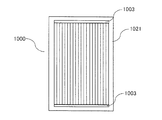
- FIG. 26 is a plan view of the thin film solar cell
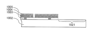
- FIG. 27 is an enlarged sectional view of the vicinity of the end of the thin film solar cell.
- a thin-film solar cell 1000 disclosed in Patent Document 1 has a structure in which a region 1021 (an insulating portion in Patent Document 1) where the insulating substrate is exposed at the peripheral edge of the insulating substrate 1002 exists.
- a transparent electrode layer 1003, a semiconductor layer 1004, and a back electrode layer 1005 are formed over the insulating substrate 1002, and then the transparent electrode layer 1003, the semiconductor layer 1004, and A method of exposing an insulating substrate by removing a part of the back electrode layer 1005 is disclosed.
- the region 1021 where the insulating substrate is exposed is a portion that becomes a part of the insulating portion between the photoelectric conversion element portion and the metal frame when the thin film solar cell module is manufactured, and originally exists on the insulating substrate.
- some material residue may be present even if each layer is removed by laser light. If there is a residue, when it is a solar cell module, sufficient insulation performance cannot be obtained between the photoelectric conversion element and a member such as a metal frame.
- the thin-film solar cell module As described above, it is not sufficient for the thin-film solar cell module to provide an insulating portion in terms of design, and it is necessary to actually inspect and confirm the insulating performance. It is better to inspect the insulation performance earlier in the manufacturing process and find the nonconforming product than to measure the insulation performance after mounting the metal frame around the thin film solar cell and find the nonconforming product. This is desirable. This is because the non-conforming product does not need to be subjected to subsequent manufacturing processes.
- Patent Document 2 Japanese Patent Application Laid-Open No. 2005-236051 is an example of a method for inspecting insulation performance before a metal frame is attached to a thin film solar cell.
- a method for inspecting a thin film solar cell module (photoelectric conversion panel in Patent Document 2) in which a transparent support substrate, a photoelectric conversion element, and a moisture-proof sheet obtained by sandwiching a metal thin film with a resin thin film are stacked in this order.
- inspection of the insulation performance of a thin film solar cell module by inspecting the insulation performance between the circuit of a photoelectric conversion element, and the metal thin film of a moisture-proof sheet is disclosed.
- a nonconforming product can be found before the metal frame is attached to the thin film solar cell. Since the insulation performance is measured by using the metal thin film in the moisture-proof sheet covering the photoelectric conversion element and the photoelectric conversion panel as an electrode material, it is easy to inspect the insulation performance for the entire surface of the solar cell module body. And can be done quickly.
- JP 2008-109041 A Japanese Patent Laid-Open No. 2005-236051
- the conventional method for inspecting the insulation performance of the entire surface only measures the whole surface, so it is possible to determine whether or not there is a defective insulation part, but the approximate position of the defective insulation part is not known. there were.
- the present invention has been made in view of the above problems, and its purpose is to specify the location of an insulation failure portion in the inspection of the insulation performance of the peripheral portion of a thin film solar cell.
- the thin-film solar cell inspection apparatus, the thin-film solar cell inspection method, the thin-film solar cell manufacturing method, and the thin-film solar cell manufacturing system of the present invention employ the following configurations.
- a thin-film solar cell inspection apparatus includes an insulating substrate, a transparent electrode layer, a semiconductor layer, and a back electrode layer sequentially stacked on the insulating substrate, and is insulated at a peripheral portion of the insulating substrate.
- An inspection apparatus for a thin-film solar cell having a region where a substrate is exposed.
- the inspection apparatus for a thin-film solar cell includes a first terminal that contacts at least one of the transparent electrode layer or the back electrode layer, a second terminal that contacts at least one of the region where the insulating substrate is exposed or the outer peripheral edge of the insulating substrate, A voltage applying unit that applies a voltage between the first terminal and the second terminal; a current detecting unit that detects a current flowing between the first terminal and the second terminal; and a moving mechanism. At least one of the first terminal or the second terminal is divided into a plurality of individual terminals. The moving mechanism moves each individual terminal.
- an inspection apparatus for a thin-film solar cell includes an insulating substrate, a transparent electrode layer, a semiconductor layer, and a back electrode layer that are sequentially stacked on the insulating substrate, and the insulating substrate is provided at the periphery of the insulating substrate. It is an inspection apparatus of the thin film solar cell which has the area
- the inspection apparatus for a thin-film solar cell includes a first terminal that contacts at least one of the transparent electrode layer or the back electrode layer, a second terminal that contacts at least one of the region where the insulating substrate is exposed or the outer peripheral edge of the insulating substrate, A third terminal that is in contact with a region where the insulating substrate is exposed between a portion where one terminal abuts and a portion where the second terminal abuts, and two of the first terminal, the second terminal, and the third terminal.
- a voltage application unit that applies a voltage between two terminals, a current detection unit that detects a current flowing between the terminals to which the voltage is applied, and a moving mechanism are provided.
- the third terminal is divided into a plurality of individual terminals. The moving mechanism moves each individual terminal.
- the individual terminals are divided for each side of the insulating substrate.
- At least one of the first terminal, the second terminal, and the third terminal is divided into a plurality of portions in the length direction of the side on at least one side of the insulating substrate. Yes.
- a method for inspecting a thin-film solar cell includes an insulating substrate, a transparent electrode layer, a semiconductor layer, and a back electrode layer that are sequentially stacked on the insulating substrate, and is insulated at a peripheral portion of the insulating substrate. It is an inspection method for an inspection apparatus to inspect a thin film solar cell having a region where a substrate is exposed.
- the inspection apparatus includes a first terminal that contacts at least one of the transparent electrode layer and the back electrode layer, and a second terminal that contacts at least one of the region where the insulating substrate is exposed or the outer peripheral end of the insulating substrate. At least one of the first terminal and the second terminal is divided into a plurality of individual terminals and is moved by a moving mechanism.
- the inspection method includes an abutting process for abutting one of the individual terminals, an abutting process for abutting a terminal corresponding to the abutted terminal, and an insulation for inspecting insulation performance between the abutted terminals. And a performance inspection process.
- a method for inspecting a thin-film solar cell includes an insulating substrate, a transparent electrode layer, a semiconductor layer, and a back electrode layer that are sequentially stacked on the insulating substrate, and is insulated at a peripheral portion of the insulating substrate. It is an inspection method for an inspection apparatus to inspect a thin film solar cell having a region where a substrate is exposed.
- the inspection apparatus has a first terminal that contacts at least one of the transparent electrode layer or the back electrode layer, a second terminal that contacts at least one of the region where the insulating substrate is exposed or the outer peripheral edge of the insulating substrate, and the first terminal.
- the inspection method includes an abutting process for abutting one of the individual terminals, an abutting process for abutting the first terminal or the second terminal corresponding to the abutting terminal, and insulation performance between the abutting terminals.
- the method for inspecting a thin film solar cell performs an abutting step for abutting all the individual terminals, an abutting step for abutting the terminals corresponding to the individual terminals, and an insulation performance between the abutted terminals. Compare the insulation performance inspection process with the reference value that holds the inspection result in advance, determine whether to contact each individual terminal individually, and contact each individual terminal according to the result of the determination process And a contacting step.
- the method for manufacturing a thin film solar cell includes an insulating substrate, a transparent electrode layer sequentially laminated on the insulating substrate, a semiconductor layer, a back electrode layer, and a thin film having a region where the insulating substrate is exposed at a peripheral portion of the insulating substrate. It has the test
- the method for manufacturing a thin-film solar cell includes a removal step of removing a cause of defective insulation.
- the removal process is performed based on the result of the inspection process.
- the thin-film solar cell manufacturing system includes a thin-film solar cell inspection apparatus according to the present invention, and a thin-film solar cell removal apparatus that removes an insulation failure cause existing in a region where the insulating substrate is exposed at the peripheral edge of the insulating substrate.
- the control unit of the removal device controls the processing unit based on the inspection information from the inspection device.
- inspection apparatus It is a figure which shows the combination of the terminal to which the voltage is applied of the inspection apparatus of the thin film solar cell in the 3rd Embodiment of this invention.
- FIG. 1 is an explanatory diagram of a thin-film solar cell inspection apparatus according to this embodiment.
- the thin film solar cell inspection apparatus according to the present embodiment is an inspection apparatus for inspecting the thin film solar cell 100 for the insulating performance of the region 21 where the insulating substrate is exposed.
- the thin film solar cell 100 includes an insulating substrate 2 having a main surface 2s, and a photoelectric conversion element including a transparent electrode layer 3, a semiconductor layer 4, and a back electrode layer 5 sequentially stacked on the main surface 2s of the insulating substrate 2.
- a photoelectric conversion element including a transparent electrode layer 3, a semiconductor layer 4, and a back electrode layer 5 sequentially stacked on the main surface 2s of the insulating substrate 2.
- the peripheral portion of the insulating substrate 2 there is a region 21 where the insulating substrate 2 where the main surface 2 s of the insulating substrate 2 is exposed is exposed.
- the inspection apparatus includes first terminals 611 and 612 that are a plurality of individual terminals for contacting the back surface electrode layer 5, a second terminal 62 for contacting the outer peripheral edge of the insulating substrate, a first terminal 611, 612 flows through the moving mechanisms 711 and 712, the voltage applying unit 8 for applying a voltage between the first terminal and the second terminal, and the two terminals to which the voltage is applied by the voltage applying unit 8. And a current detection unit 9 for detecting current.
- the outer peripheral edge of the insulating substrate is the end surface of the insulating substrate.
- the moving mechanism is a mechanism for bringing a terminal and an inspection object into contact with or apart from each other, and does not represent only a case where the terminal moves in a vertical direction with respect to the main surface 2s of the substrate, but includes a case where the terminal and the inspection object move with an angle.
- the inspection device uses the moving mechanisms 711 and 712 so as to separate the first terminal 611. That is, there are two first terminals, but there is one first terminal that is in contact with the back electrode layer 5 when a voltage is applied.
- the voltage application part 8 and the electric current detection part 9 in FIG. 1 are shown typically. There may be two voltage application units 8 and current detection units 9 corresponding to the first terminals 611 and 612, respectively, and one voltage application unit 8 and current detection unit 9 may be divided into conductive wires. And may be connected to both of the two first terminals. It is desirable to share it because the parts of the inspection apparatus can be reduced and the cost of the apparatus can be reduced.
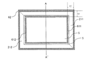
- FIG. 2 is a schematic plan view of the thin film solar cell and the terminal of the inspection device as viewed from above the inspection device.
- the first terminal for contacting the back electrode layer is composed of two terminals, a first terminal 611 and a first terminal 612, and the second terminal 62 for contacting the outer peripheral edge of the insulating substrate is insulated. It is integrally formed along the outer peripheral edge of the substrate.
- FIG. 1 corresponds to a cross section taken along the line AA ′ in FIG.
- the distance t1 between the first terminal 611 and the second terminal 62 is about 12 mm.
- the moving mechanism may also be attached to the second terminal 62.
- the inspection apparatus can bring the second terminal into contact with the outer peripheral edge of the insulating substrate from the back electrode layer side of the thin-film solar cell by providing a moving mechanism on the second terminal 62.
- the inspection apparatus may be provided with a mechanism that moves to the left and right so that the second terminal contacts the outer peripheral edge of the insulating substrate from the end surface side of the substrate.
- FIG. 3 is an explanatory diagram of combinations of different terminals to which a voltage is applied. Similar to FIG. 1, a cross section taken along the line AA ′ in FIG. 2 corresponds to FIG. 3.
- the voltage applying unit 8 can apply a voltage to the combinations C ⁇ b> 1 and C ⁇ b> 2 by causing the inspection device to bring either the first terminal 611 or 612 into contact with the back electrode 5.
- the inspection apparatus applies a voltage between the first terminal 611 and the second terminal 62 or between the first terminal 612 and the second terminal 62 and detects a current flowing between the two terminals. Insulation performance can be inspected. That is, since the first terminal is divided into two parts instead of a single body, the inspection apparatus has an insulation failure portion in either the region 211 or 212 where the peripheral insulating substrate shown in FIG. 2 is exposed. It can be specified.
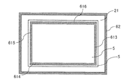
- FIG. 4 is a plan view of the thin film solar cell and the terminal of the inspection device according to the modification of the first embodiment when viewed from above the inspection device. 4 is different from FIG. 2 in that the first terminal is divided into four corresponding to the number of sides. Since each of the first terminals 613, 614, 615, and 616, which are individual terminals, has a moving mechanism, the inspection apparatus can inspect the insulation performance for each side. Such a thin-film solar cell inspection apparatus can specify which side of the region where the insulating substrate is exposed has an insulation failure portion.
- the first terminal is desirably divided into three.
- the terminal is desirably divided into the number of sides corresponding to each side of the insulating substrate.
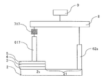
- FIG. 5 shows a thin-film solar cell inspection apparatus according to a modification of the first embodiment.
- the same thin-film solar cell inspection apparatus as that in FIG. 1 is used, an example is shown in which the second terminal 62a abuts on the main surface 2s of the region 21 where the insulating substrate at the peripheral edge of the insulating substrate is exposed.
- the first terminal 617 contacts the transparent electrode layer 3 by the moving mechanism 717 as in FIG. Since the inspection apparatus can shorten the distance between the first terminal 617 and the second terminal 62a by bringing the second terminal 62a into contact with the main surface 2s of the insulating substrate 2, the insulation performance can be measured more accurately. It becomes possible to do.
- FIG. 6 shows a thin-film solar cell inspection apparatus according to a modification of the first embodiment.
- the same thin-film solar cell inspection apparatus as that in FIG. 1 is used, an example in which the first terminal 618 contacts the transparent electrode layer 3 by the moving mechanism 718 is shown. It differs from the example shown so far in that the transparent electrode layer 3 of the thin film solar cell protrudes to the outer peripheral side from the photoelectric conversion layer 4 and the back electrode layer 5.
- the other points are the same, and the same action and effect can be obtained even when the first terminal 618 is brought into contact with the transparent electrode layer 3.
- the first terminal since the first terminal only needs to be electrically connected to the photoelectric conversion element, the first terminal may be in contact with either the transparent electrode layer or the back electrode layer. In other words, at least a part of the first terminal only needs to be in contact with the electrode of the thin film solar cell.
- the inspection device is configured such that the first terminal and the second terminal are in contact with the transparent electrode layer. Since the distance to the terminal is shortened, the insulation performance can be accurately measured. Moreover, if a load is applied to the back electrode layer, the semiconductor layer of the photoelectric conversion element may be scratched, and a short circuit may occur between the transparent electrode layer and the back electrode layer. In order to avoid a short circuit, it is desirable to contact the terminal with the transparent electrode layer.
- the inspection apparatus causes the first terminal to abut the transparent electrode layer on the side having the protruding structure. Other sides may be in contact with the back electrode layer. The reason is that it is possible to avoid a short circuit between the transparent electrode layer and the back electrode layer due to scratches on the semiconductor layer of the photoelectric conversion element.
- the thin-film solar cell to be inspected does not necessarily have to be completed as a photoelectric conversion element in which all of the transparent electrode layer, the semiconductor layer, and the back electrode layer are formed. Good. This is the same in other embodiments.
- the inspection apparatus for a thin-film solar cell according to the second embodiment will be described below with reference to the drawings.
- the inspection apparatus according to the second embodiment is different from the first embodiment in that the first terminal is an integral type and the second terminal is divided and has a moving function.
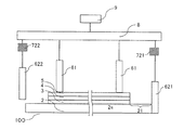
- FIG. 7 is an explanatory diagram when a thin film solar cell is inspected by an inspection apparatus including second terminals 621 and 622 which are a plurality of individual terminals, and each individual terminal includes moving mechanisms 721 and 722.
- the first terminal 61 is an integral type.
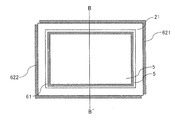
- FIG. 8 is an explanatory diagram when the terminals of the thin-film solar cell inspection device shown in FIG. 7 are viewed from the upper side of the inspection device.
- the BB ′ cross section of FIG. 8 corresponds to FIG.
- the inspection apparatus according to the second embodiment differs from the inspection apparatus according to the first embodiment only in the types of terminals to be divided, and the operations and effects are the same. Moreover, even if both the first terminal and the second terminal are divided, the operation and effect are the same.
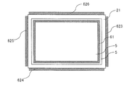
- FIG. 9 is a plan view when a terminal of the inspection device for a thin-film solar cell according to a modification of the second embodiment is viewed from above the inspection device.
- the second terminal is divided into four corresponding to the number of sides. Since each of the second terminals 623, 624, 625, and 626, which are a plurality of individual terminals, has a moving mechanism, the inspection apparatus according to the present embodiment can inspect the insulation performance for each side.
- the difference from the example described with reference to FIG. 4 in the first embodiment is only whether the divided terminals are the first terminal or the second terminal. This is the same as described with reference to FIG. Therefore, the terminal of the inspection apparatus divided into the number of sides corresponding to each side of the insulating substrate of the thin-film solar cell may be either the first terminal or the second terminal, or the first terminal and the second terminal. Both are good.
- the inspection apparatus according to the third embodiment differs from the inspection apparatus according to the first embodiment in that the first terminal and the second terminal are integrated, the third terminal is provided, and The three terminals are divided into a plurality of individual terminals, each having a moving mechanism.
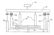
- FIG. 10 is an explanatory diagram of a thin-film solar cell inspection apparatus according to this embodiment.
- the inspection apparatus includes a first terminal 61 for contacting the back electrode layer 5, a second terminal 62 for contacting the outer peripheral edge of the insulating substrate, and an individual terminal contacting the region 21 where the insulating substrate is exposed.
- the voltage application unit 81 applies a voltage between two terminals selected from a total of four terminals, three types of first terminal 61, second terminal 62, third terminal 631, and third terminal 632. To do.
- the third terminal 632 is separated when the third terminal 631 is in contact with the region 21 where the insulating substrate is exposed, and the third terminal 631 is separated when the third terminal 632 is in contact.
- the moving mechanisms 731 and 732 are used.
- Each or both of the first terminal 61 and the second terminal 62 may have a moving mechanism.
- the voltage application part 81 and the electric current detection part 91 in FIG. 10 are shown typically.
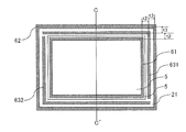
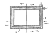
- FIG. 11 is a plan view of the terminal of the thin-film solar cell inspection device according to the third embodiment as viewed from above the inspection device.
- the third terminal that contacts the region 21 where the insulating substrate is exposed is divided into a third terminal 631 and a third terminal 632, and the first terminal 61 and the second terminal 62 are integrated.
- the distance t2 between the first terminal 61 and the third terminal 631 is 5 mm
- the distance t3 between the third terminal 631 and the second terminal 62 is 6 mm.
- the width of the third terminal 631 is 1 mm.
- FIG. 10 corresponds to a cross section taken along the line CC ′ in FIG.
- the inspection apparatus knows which part of the peripheral portion of the insulating substrate has the defective insulation portion by contacting only one of the third terminal 631 and the third terminal 632 with the region 21 where the insulating substrate is exposed. Can do.
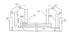
- FIG. 12 is an explanatory diagram of a combination of terminals to which a voltage is applied.
- the voltage application unit 81 can apply a voltage to the combinations C1, C2, C3, C2 ′, and C3 ′. It is desirable for the inspection apparatus to apply a voltage to all the combinations of these terminals and measure the current, but this is not a requirement.
- the inspection apparatus can specify the location of the defective insulation portion more finely by applying the voltage sequentially to both the combinations C1 and C2.
- the inspection apparatus can perform a finer inspection by applying a voltage to the combination C3, and can increase the accuracy of the insulation inspection.
- the inspection device selects the terminal used for measurement. May be.
- FIG. 11 shows the case where the third terminal is divided into two from the rectangular frame
- the third terminal may be divided into four corresponding to each side of the insulating substrate. Since the third terminal is divided corresponding to each side, the inspection apparatus can specify the location where the defective insulation portion exists, and thus the apparatus for removing the defective insulation is efficient. It is possible to remove the defective insulation portion well.
- FIG. 13 shows a thin-film solar cell inspection apparatus according to a modification of the third embodiment.
- the third terminal of the thin-film solar cell inspection device is divided into a plurality of individual terminals, and a plurality of third terminals exist in parallel to each side.
- the first terminal 61 and the second terminal 62 are integrated.
- the distance t4 between the first terminal 61 and the third terminal 634a was 3 mm
- the distance t5 between the third terminal 634a and the third terminal 634b was 3 mm
- the distance t6 between the third terminal 634b and the second terminal 62 was 4 mm.
- the width of the third terminal is 1 mm.
- the inspection device becomes more accurate with insufficient insulation performance. Can be specified. However, if the number of third terminals is increased too much, the structure of the inspection apparatus becomes complicated, and therefore the number of third terminals is preferably about two.
- the third terminal moves
- either or both of the first terminal and the second terminal may be individually divided to have a moving mechanism.
- the inspection apparatus may have a common moving mechanism so that the first terminal and the third terminal can be moved simultaneously.
- terminal division examples and shape examples that can be applied to the first to third embodiments will be described.
- 14 to 16 are examples of the division of the first terminal, the second terminal, and the third terminal. These examples can be used in any of the first to third embodiments.
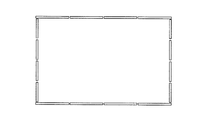
- the terminal may have a shape divided into two or four in each side.
- 14 and 15 exemplify a form in which the terminals are divided into the same number on all sides, but the present invention is not limited to this, and the terminals on each side are divided into different numbers. Also good.
- the inspection device may be arranged with columnar terminals.
- the terminal may be a prism instead of a cylinder.
- the terminals need not have the same shape along all sides of the substrate, and may be a combination of the examples shown so far.
- the inspection device in which the terminals are finely divided from the rectangular frame shape and provided with a moving mechanism in each of the terminals is a peripheral portion of the insulating substrate of the thin film solar cell, and the location of the defective insulation portion is described in more detail. Can be identified.
- the inspection apparatus can estimate which process has a problem by specifying the location of the defective insulation portion, the inspection apparatus can also be used to identify the cause of the failure in the manufacturing process.
- the first terminal is divided into the number of individual terminals corresponding to each side, and the second terminal is divided in structure, but when it is brought into contact with the insulating substrate It is explanatory drawing when the terminals are contacting.
- the configuration shown in FIG. 17 can be used in any of the first to third embodiments.
- the first terminals 619a, 619b, 619c, 619d and the second terminals 629a, 629b, 629c, 629d exist so as to correspond to each side.
- the difference from the example shown in FIG. 4 is that although the second terminal is divided into four structurally, the four terminals are adjacent if they are brought into contact with the insulating substrate. This is the point where the terminals to be touched.
- the maintenance is easier than the integrated terminal, and even if the terminal is damaged, it is possible to cope with a part of the replacement.
- FIG. 17 described the case of the second terminal.
- the first terminal may be the first terminal or both the first terminal and the second terminal may be adjacent to each other when they are divided in structure and contact with each other.
- FIGS. 18A and 18B the location where the second terminal contacts when the end of the insulating substrate 2 of the thin-film solar cell has a semicircular shape will be described.
- the configuration shown in FIGS. 18A and 18B can be used in any of the first to third embodiments.
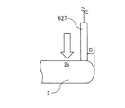
- the inspection apparatus when the second terminal 627 is brought into contact with the insulating substrate 2 with respect to the substrate having a semicircular end, the second terminal 628 is placed on the end surface of the insulating substrate 2 as shown in FIG. By abutting, it is possible to surely abut the true end.
- FIG. 18B when the second terminal 627 is brought into contact with the main surface of the insulating substrate 2, the main surface 2s must be brought into contact with a flat portion, and the inspection apparatus is , The distance D from the true end is measured inside.
- the end of the insulating substrate has a semicircular shape, but it is not limited to a semicircular shape.
- a glass substrate is often used as the insulating substrate, and in that case, the end portion is chamfered from the viewpoint of safety in the manufacturing process.
- the inspection device abuts the second terminal from the side as shown in FIG. 18A from the viewpoint that it can surely abut the true end.
- a conductive film may be laminated on the substrate end face. More specifically, a metal layer made of Ag, Al, or the like used as a back electrode layer that wraps around the end face of the insulating substrate when SnO 2 is generally used as a transparent electrode layer of a thin film solar cell. In addition, there is a wraparound during the formation of a transparent conductive film such as ZnO that may be formed between the semiconductor layer and the metal layer. From the viewpoint that the inspection apparatus measures the insulation performance more accurately including the state of the end face, it is desirable that the second terminal is brought into contact with the side face.
- the inspection apparatus can stabilize the position of the insulating substrate by bringing the second terminal into contact with the end surface of the insulating substrate from the side surface. Therefore, it is not necessary to prepare a separate member for fixing the substrate, and the effect of reducing the cost of the inspection apparatus can be obtained.
- FIG. 19 is a diagram illustrating an example of the shape of the terminal of the inspection apparatus according to the present embodiment.
- the configuration shown in FIG. 19 can be used in the first embodiment and the second embodiment.
- the inspection terminal may have a different shape for the first terminal and the second terminal.
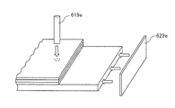
- the first terminal 619e may have a rod shape
- the second terminal 629e may have a plate shape that extends long.
- the inspection apparatus has a long extending plate in which a rod-shaped member as a first terminal is brought into contact with the back electrode from a direction perpendicular to the main surface 2s of the substrate, and is arranged in parallel with each side of the insulating substrate as a second terminal.
- a plurality of shaped terminals are arranged along each side of the insulating substrate of the thin film solar cell and are in contact with the insulating substrate from the side.
- the first terminal contacts the electrode of the thin-film solar cell. Therefore, even if the terminal is in the form of a bar, electrical connection is sufficiently possible, and the use of the bar can avoid complication of the inspection apparatus. Further, the second terminal has a plate-like shape that extends long, and thus has an effect of increasing the measurement accuracy of the inspection and measurement of the insulation performance. In addition, since the inspection device causes the second terminal to contact the insulating substrate from the side, the substrate fixing member of the inspection device is not necessary, and the number of components of the inspection device can be reduced.
- FIG. 20 is a diagram illustrating an example of the shape of the terminal of the inspection apparatus according to the present embodiment.
- the configuration shown in FIG. 20 can be used in the third embodiment.
- the first terminal 619f has a rod shape
- the second terminal 629f and the third terminals 638a and 638b have a plate shape extending long.
- the inspection device can measure with higher accuracy by making the third terminal into a plate shape extending long. The reason is that the larger the area that the third terminal is in contact with the region where the insulating substrate is exposed, the higher the possibility that it will come into contact with a cause of poor insulation that causes a decrease in insulation.
- the inspection apparatus causes the first terminal 619f to contact the back electrode layer 5 of the thin-film solar cell from the direction perpendicular to the surface of the insulating substrate, the second terminal 629f to contact the end surface of the insulating substrate from the side, and the third terminal 638a. , 638b is brought into contact with the region 21 where the insulating substrate at the periphery of the substrate is exposed from a direction perpendicular to the surface of the insulating substrate.
- a total of eight terminals are arranged, two for each side as first terminals, and a total of four plate-like terminals divided into four so as to correspond to each side as second terminals.
- a total of eight plate-like terminals divided into four pieces corresponding to each side as two third terminals are arranged in parallel to each side.
- the inspection apparatus in which the terminals are arranged in this way can measure with high accuracy while preventing an increase in cost of the apparatus.
- FIG. 21 is a flowchart of a method for inspecting a thin-film solar cell according to this embodiment.
- the inspection method for a thin film solar cell according to the present embodiment is an inspection method for inspecting a thin film solar cell for an insulating performance of an insulating portion at a peripheral portion of a substrate and identifying a location where insulation is insufficient.
- At least one of the first terminals is in contact with the electrode layer of the thin-film solar cell (S is a step; the same applies hereinafter) and the second terminal is connected to the inspection method.
- Step S2 for contacting the outer peripheral edge of the substrate;
- Voltage application step S3 for applying a voltage between the contacted terminals;
- Current detection step S4 for detecting a current between the terminals;
- a step S5 for separating the first terminal, a step S6 for bringing the other one of the first terminals into contact with the electrode layer, a voltage applying step S7 for applying a voltage between the terminals, and a current detecting step S8 for detecting a current between the terminals.
- the voltage application step S3 and the current detection step S4, or the voltage application step S7 and the current detection step S8 are collectively referred to as an insulation performance inspection step.
- Step S1 is a step in which one of the first terminals contacts the back electrode layer or the transparent electrode layer of the thin film solar cell, and the other first terminals are in a separated state.
- Steps S1 and S2 are not necessarily performed in this order, and step S1 may be performed after step S2. Moreover, process S1 and process S2 may be performed simultaneously.
- the voltage application step S3 and the current detection step S4 may be performed a plurality of times for each different combination of terminals, and each time the selected combination of terminals is changed, as a preparation, the steps S1 and S2 The necessary steps are performed.
- the current detection step S4 is performed after the application is started by the voltage application step S3 and before the application is finished. Therefore, the current detection step S4 is performed during a part of the time zone during which the voltage application step S3 is performed. In this way, the inspection device applies a voltage for each combination by bringing a plurality of terminals into contact with each other and inspects whether or not a current flows, so that where the insulation failure occurs is on the substrate. Can know.
- FIG. 22 shows another example of a method for inspecting a thin film solar cell according to the present embodiment.
- a difference from the inspection method shown in FIG. 21 is that there is a step of determining whether or not the first terminals are brought into contact individually.
- the inspection method includes a step S11 in which all of the first terminals which are a plurality of individual terminals are brought into contact with the electrode layer, a step S12 in which the corresponding second terminal is brought into contact with the outer peripheral edge of the substrate, and a substrate peripheral portion of the thin film solar cell.
- a voltage application step S13 for applying a voltage to the whole
- a current detection step S14 for detecting a current flowing between the terminals
- a current value detected in step S14 is compared with a reference value held in advance, and a plurality of results are obtained.
- determining step S15 for determining whether or not the first terminals, which are individual terminals, are brought into contact with each other.
- step S15 if the detected current is less than the reference value, the inspection is terminated, and if it is greater than the reference value, it is determined that the next step in the inspection method is to be performed. This is because if the voltage is applied to the entire periphery of the thin-film solar cell and the detected current value is small, the inspection apparatus can determine that there is no defective insulation in the region where the insulating substrate is exposed. That is, the inspection apparatus determines whether the insulation performance between the terminals is sufficient. More specifically, the inspection apparatus applies a voltage of 6000 V between the first terminal and the second terminal, and determines that the inspection is completed when a current of 50 ⁇ A or more is not detected. The inspection apparatus can select thin-film solar cells that do not need to determine where insulation failure has occurred by performing the processes of steps S11 to S15, and increase production efficiency by eliminating unnecessary processes. be able to.
- the step S16 when the inspection apparatus determines that the first terminals, which are individual terminals, are brought into contact with each other, the step S16 of bringing one of the first terminals into contact with the electrode layer and the corresponding second terminal A step S17 for contacting the outer peripheral edge of the substrate, a voltage applying step S18 for applying a voltage between the two contacted terminals, and a current detecting step S19 for detecting a current between the terminals are performed.
- the inspection method shown in FIG. 22 is more preferable than the inspection method shown in FIG. 21 because the insulation inspection of the peripheral edge of the substrate of the thin film solar cell can be performed efficiently.
- FIG. 23 is a flowchart of a method for inspecting a thin-film solar cell according to this embodiment.
- the inspection method includes a step S21 in which the first terminal is brought into contact with the electrode layer of the thin film solar cell or the second terminal is brought into contact with the outer peripheral edge of the substrate, and one of the third terminals, which are individual terminals, is insulated at the periphery of the substrate.
- Step S25 for separating the contacted third terminal from the region where the insulating substrate is exposed, Step S26 for bringing the other third terminal into contact with the region where the insulating substrate is exposed, and applying a voltage between the terminals.
- Voltage application step S27 and current detection step S28 for detecting the current between the terminals.
- the voltage application step S23 and the current detection step S24, or the voltage application step S27 and the current detection step S28 are collectively referred to as an insulation performance inspection step.
- step S21 the inspection apparatus causes the first terminal to contact the back electrode layer or the transparent electrode layer of the thin film solar cell, or causes the second terminal to contact the substrate outer peripheral edge.
- step S22 one of the plurality of third terminals, which are individual terminals, is in contact with the insulating region where the insulating substrate at the peripheral edge of the thin film solar cell is exposed, and the other third terminals are not in contact. State. Steps S21 and S22 are not necessarily performed in this order, and the order may be changed. Steps S21 and S22 may be performed simultaneously. However, before the voltage application step S23 is performed, it is necessary that two necessary terminals to be applied with voltage are in contact with the corresponding locations.
- Steps S23 and S24 may be performed a plurality of times for each different combination of terminals, and each time a combination of selected terminals is changed, a necessary step from among steps S21 and S22 is performed as a preparation. It may be done.
- the current detection step S24 is performed after the application is started by the voltage application step S23 and before the application is finished. Therefore, step S24 is performed during a part of the time zone during which step S23 is performed.
- the inspection device knows where the insulation defect occurs on the board by inspecting whether the current flows by applying a voltage for each combination by bringing a plurality of terminals into contact with each other. Can do.
- the inspection method according to the present embodiment may further include a step of determining whether or not the terminals need to be brought into contact individually.
- FIG. 24 is a flowchart of the method for manufacturing the thin-film solar cell according to this embodiment.
- the manufacturing method includes a carry-in process S31, a photoelectric conversion element formation process S32, an insulation region formation process S33, an inspection process S34, a determination process S35, an insulation failure cause removal process S36, and a power generation performance evaluation process S37. Unloading step S38.
- the thin film solar cell 100 described with reference to FIG. 1 shows a state in which the insulating region forming step S33 has been performed, and will be referred to in the description of the following steps.
- a carrying-in apparatus (not shown) carries in the insulating substrate 2 in the production line of a thin film solar cell.
- the photoelectric conversion element forming apparatus (not shown) forms the photoelectric conversion element by sequentially laminating the transparent electrode layer 3, the semiconductor layer 4, and the back electrode layer 5 on the insulating substrate 2. .
- Each layer is formed by a method such as plasma CVD, sputtering, or vapor deposition by the photoelectric conversion element forming apparatus.
- the photoelectric conversion element formation apparatus does not necessarily form all of the transparent electrode layer 3, the semiconductor layer 4, and the back surface electrode layer 5 in the photoelectric conversion element formation step S32.
- the photoelectric conversion element forming apparatus performs the processes after the formation of the semiconductor layer 4 in the photoelectric conversion element forming process S32. May be performed.
- the insulating region forming apparatus uses the insulating region forming apparatus to remove the transparent electrode layer 3, the semiconductor layer 4, and the back electrode layer 5 in the predetermined region at the peripheral portion of the insulating substrate 2. By removing, the region 21 where the insulating substrate is exposed is formed.
- the insulating region forming apparatus is, for example, a polishing apparatus using a rotating polishing disk, a blast apparatus that removes a film by spraying grains, or a laser processing apparatus that evaporates a film by irradiating a laser.
- the inspection apparatus shown in the first to third embodiments inspects the insulating performance of the peripheral portion of the thin film solar cell.
- the inspection result is compared with the reference value, and the thin-film solar cell that is determined to have insufficient insulation performance is referred to as an insulation failure cause removal step S36 (hereinafter also simply referred to as “removal step S36”). Turn.
- the thin film solar cell determined to have sufficient insulation performance is subjected to the power generation performance evaluation step S37.
- the defective insulation cause removing device removes the defective insulation cause of the thin-film solar cell in which the position of the defective insulation portion is specified.
- the cause of poor insulation include wraparound during film formation of the transparent electrode layer, semiconductor layer and / or back electrode layer, and residues during formation of the region 21 where the insulating substrate is exposed.
- the removal device is, for example, a polishing device, a blast device or a laser processing device, a wiping device that removes a cause of insulation failure by wiping with a cloth soaked with a liquid such as pure water or an organic solvent.
- the removal device can be replaced by the insulating region forming device used in the insulating region forming step S33.
- the operating conditions of the apparatus such as shortening the processing time, pressing during polishing and lowering the laser irradiation energy, etc. It is desirable to make changes.
- laser processing can shorten the processing time with linear processing rather than processing with an angle that bends at a right angle, so the side where the insulation performance is insufficient is located on which side. It is desirable to specify whether it exists.
- the solar simulator that evaluates the power generation performance by irradiating pseudo-sunlight evaluates the power generation performance of the thin-film solar cell.
- a conveying apparatus may convey a thin film solar cell to test
- the unloading device unloads the thin film solar cell. Thereafter, other performance inspections and manufacturing processes of the thin-film solar cell module are performed as necessary.
- the removal device when there are few thin film solar cells for which the removal step S36 is determined to be necessary, the removal device is installed independently of the production line in which the devices of other processes are installed so as to be able to carry in series. It may be. In this case, it is only necessary to install an independent transport device that can be transported between the inspection device and the removal device, while being installed so as to be transportable between the inspection device and the power generation performance evaluation device. Or you may provide the storage shelf which temporarily stores a thin film solar cell, without installing an independent conveying apparatus, and may convey to a removal apparatus from a storage shelf.
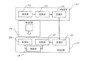
- FIG. 25 shows a schematic explanatory diagram of a thin-film solar cell manufacturing system according to this embodiment.
- This system includes an inspection device K1, an insulation failure cause removal device Z1, and a transfer device H1.
- the inspection device K1 includes an inspection unit K2, a storage unit K3, and a communication unit K4.
- the insulation failure cause removing device Z1 (hereinafter also referred to as “removing device Z1”) includes a communication unit Z2, a storage unit Z3, a control unit Z4, and a processing unit Z5.
- the communication unit K4 of the inspection device and the communication unit Z2 of the removal device Z1 transmit information to each other.
- the transport device H1 transports the thin-film solar cell between the inspection device K1 and the removal device Z1.
- the inspection unit K2 of the inspection apparatus uses any of the inspection apparatuses shown in the first to third embodiments.
- the inspection device K1 stores the inspection information detected by the inspection unit K2 in the storage unit K3.
- the inspection information includes position information that identifies the location of the defective insulation and thin film solar cell identification information that can identify the thin film solar cell.
- the inspection device K1 and the removal device Z1 are connected to be communicable with each other.
- the inspection information stored in the storage unit K3 of the inspection device K1 is transmitted from the communication unit K4 of the inspection device K1 to the communication unit Z2 of the removal device Z1, and the removal device Z1 stores the received inspection information in the storage unit Z3. .
- the control unit Z4 of the removal device Z1 corresponds to the transferred thin film solar cell by the identification information included in the stored inspection information. Identify the test results. Further, the control unit Z4 specifies a place where the removal is performed based on the position information that specifies the location of the defective insulation contained in the inspection information. Based on the inspection information, the control unit Z4 of the removal device Z1 controls the processing unit Z5 to remove the cause of defective insulation.
- the inspection device K1 and the removal device Z1 are connected so as to be directly communicable.
- the inspection device K1 and the removal device are not included in a control device (not shown) that controls the entire thin-film solar cell manufacturing system.
- the devices Z1 may be connected so as to be able to communicate with each other.
- the inspection device K1 relays the control device that controls the entire manufacturing system of the thin-film solar cell, and transmits inspection information to the removal device Z1.
- the inspection device according to the prior art can detect the presence or absence of the cause of insulation failure, the location where the cause of insulation failure exists cannot be specified.
- the portion 21 needs to be subjected to insulation cause substance removal processing.
- the inspection device K1 specifies the position where the cause of insulation failure exists, and the removal device Z1 performs the removal process only on the place where the cause of insulation failure exists.
- the processing time for removing the causal agent can be shortened. Therefore, the manufacturing method according to the present embodiment can improve the manufacturing efficiency of the thin film solar cell.
- the present invention can be widely applied to a thin film solar cell inspection device, a thin film solar cell inspection method, a thin film solar cell manufacturing method, and a thin film solar cell manufacturing system in general.
Landscapes
- Photovoltaic Devices (AREA)
Abstract
薄膜太陽電池の絶縁性能の検査において、絶縁不良部の箇所がわからないという問題があった。よって、絶縁不良部の箇所を特定した上で絶縁不良原因物の除去を行うことができず、薄膜太陽電池の生産性があがらないという問題があった。本発明に係る薄膜太陽電池の検査装置(K1)は、端子が複数の個別端子に分割され、かつそれぞれが移動機構(711~738)を備えており、個別端子それぞれを当接させることを特徴としている。この検査装置を用いて、薄膜太陽電池の絶縁性能の検査を行うことにより、絶縁不良部の箇所を特定することができる。
Description
本発明は、薄膜太陽電池の検査装置、薄膜太陽電池の検査方法、薄膜太陽電池の製造方法、および薄膜太陽電池の製造システムに関する。
薄膜太陽電池は、半導体材料を利用した光電変換素子に太陽光等の光を入射させることによって、光電変換素子の正極と負極との間に起電力を生じさせるものである。薄膜太陽電池モジュールは、屋外に設置されることが多く、雨に打たれるなどしても漏電が生じないよう、光電変換素子と他の部材との間での絶縁性能が求められている。本願において、薄膜太陽電池とは、基板上に、少なくとも透明電極層、半導体層及び裏面電極層を有する構造をもつものを示しており、光電変換素子とは、透明電極層、半導体層及び裏面電極層からなる素子を示している。薄膜太陽電池モジュールとは、薄膜太陽電池を封止した状態を示している。
薄膜太陽電池の周辺部分に金属フレームを取り付けた薄膜太陽電池モジュールを製造する場合、規格の一つであるIEC61730によれば、例えばシステム電圧が1000Vの場合に、8.4mm以上の絶縁部分を光電変換素子部と金属フレームとの間に設けなければならないことが規定されている。
特開2008-109041号公報(特許文献1)に、薄膜太陽電池の一般的な構造が示されている。図26は薄膜太陽電池の平面図であり、図27は薄膜太陽電池の端部近傍の拡大断面図である。特許文献1に示された薄膜太陽電池1000は、絶縁基板1002の周縁部に絶縁基板が露出する領域1021(特許文献1では、絶縁部分)が存在する構造となっている。絶縁基板が露出する領域1021を形成する方法として、絶縁基板1002の上に、透明電極層1003、半導体層1004、裏面電極層1005を形成した後、レーザ光により透明電極層1003、半導体層1004及び裏面電極層1005の一部を除去することで、絶縁基板を露出させる方法が開示されている。絶縁基板が露出する領域1021は、薄膜太陽電池モジュールを製造したとき、光電変換素子部と金属フレームとの間の絶縁部分の一部になる箇所であり、本来ならば絶縁基板上に何も存在しない状態となっているべきであるが、実際には、レーザ光で各層の除去を行っても、何らかの材料の残渣が存在することがある。残渣があると、太陽電池モジュールとしたとき、光電変換素子と金属フレーム等の部材との間で十分な絶縁性能が得られなくなる。
このように、薄膜太陽電池モジュールは、設計上、絶縁部分を設けるだけでは十分とはいえず、実際に検査を行い、絶縁性能を確認する必要がある。薄膜太陽電池の周辺部分に金属フレームを装着した後に、絶縁性能を測定して不適合品を見つけるより、製造工程のより早い段階で絶縁性能の検査を行って不適合品を見つけるほうが、生産効率の向上という点からは望ましい。不適合品については以降の製造工程を施さずに済むためである。
薄膜太陽電池に金属フレームを装着する前の段階での、絶縁性能の検査方法のひとつとして、特開2005-236051号公報(特許文献2)があげられる。透明支持基板と、光電変換素子と、金属薄膜を樹脂薄膜で挟みこんでなる防湿シートとを、この順番で積層してなる薄膜太陽電池モジュール(特許文献2では、光電変換パネル)の検査方法であって、薄膜太陽電池モジュールの絶縁性能の検査を、光電変換素子の回路と、防湿シートの金属薄膜との間の絶縁性能を検査することによって行う検査方法が開示されている。この方法を用いれば、薄膜太陽電池に金属フレームを装着する前の段階で不適合品を発見できる。光電変換素子と光電変換パネルを覆っている防湿シート中の金属薄膜を電極材料として利用して、絶縁性能を測定しているので、太陽電池モジュール本体の表面全体についての絶縁性能の検査を容易、かつ迅速に行うことができる。
しかしながら、従来の表面全体についての絶縁性能の検査を行う方法では、全体測定しか行っていないため、絶縁不良部が有るか無いかは判断できるものの、絶縁不良部のおおよその位置もわからないという問題があった。
本発明は上記の問題に鑑みてなされたものであり、その目的は、薄膜太陽電池の周縁部の絶縁性能の検査において、絶縁不良部の箇所を特定することである。
上記課題を解決するために、本発明の薄膜太陽電池の検査装置、薄膜太陽電池の検査方法、薄膜太陽電池の製造方法、薄膜太陽電池の製造システムは、以下の構成を採用する。
すなわち、ある実施の形態に従うと、薄膜太陽電池の検査装置は、絶縁基板と、絶縁基板上に順次積層させた透明電極層、半導体層、裏面電極層とを含み、絶縁基板の周縁部に絶縁基板が露出する領域を有する薄膜太陽電池の検査装置である。薄膜太陽電池の検査装置は、透明電極層又は裏面電極層の少なくとも一方に当接する第1端子と、絶縁基板が露出する領域又は絶縁基板の外周端の少なくとも一方に当接する第2端子と、第1端子と第2端子との間に電圧を印加する電圧印加部と、第1端子と第2端子との間に流れる電流を検出する電流検出部と、移動機構とを備える。第1端子または第2端子の少なくとも一方は、複数の個別端子に分割される。移動機構は、個別端子をそれぞれ移動させる。
他の実施の形態に従うと、薄膜太陽電池の検査装置は、絶縁基板と、絶縁基板上に順次積層させた透明電極層、半導体層、裏面電極層とを含み、絶縁基板の周縁部に絶縁基板が露出する領域を有する薄膜太陽電池の検査装置である。薄膜太陽電池の検査装置は、透明電極層又は裏面電極層の少なくとも一方に当接する第1端子と、絶縁基板が露出する領域又は絶縁基板の外周端の少なくとも一方に当接する第2端子と、第1端子の当接する箇所と第2端子の当接する箇所との間であって、絶縁基板が露出する領域に当接する第3端子と、第1端子、第2端子及び第3端子のうちの2つの端子の間に電圧を印加する電圧印加部と、電圧を印加した端子間に流れる電流を検出する電流検出部と、移動機構とを備える。第3端子は、複数の個別端子に分割される。移動機構は、個別端子をそれぞれ移動させる。
好ましくは、薄膜太陽電池の検査装置において、個別端子は、絶縁基板の辺毎に分割されている。
好ましくは、薄膜太陽電池の検査装置において、第1端子、第2端子、第3端子の少なくとも1つの端子は、絶縁基板の少なくとも1つの辺において、辺の長さ方向に対し複数に分割されている。
さらに他の実施の形態に従うと、薄膜太陽電池の検査方法は、絶縁基板と、絶縁基板上に順次積層させた透明電極層、半導体層、裏面電極層とを含み、絶縁基板の周縁部に絶縁基板が露出する領域を有する薄膜太陽電池を検査装置が検査するための検査方法である。検査装置は、透明電極層又は裏面電極層の少なくとも一方に当接する第1端子と、絶縁基板が露出する領域又は絶縁基板の外周端の少なくとも一方に当接する第2端子とを備える。第1端子、第2端子の少なくとも一方の端子は複数の個別端子に分割され、移動機構によりそれぞれ移動するものである。検査方法は、個別端子の1つを、当接させる当接工程と、当接した端子に対応する端子を、当接させる当接工程と、当接した端子間の絶縁性能の検査を行う絶縁性能検査工程とを有する。
さらに他の実施の形態に従うと、薄膜太陽電池の検査方法は、絶縁基板と、絶縁基板上に順次積層させた透明電極層、半導体層、裏面電極層とを含み、絶縁基板の周縁部に絶縁基板が露出する領域を有する薄膜太陽電池を検査装置が検査するための検査方法である。検査装置は、透明電極層又は裏面電極層の少なくとも一方に当接する第1端子と、絶縁基板が露出する領域又は絶縁基板の外周端の少なくとも一方に当接する第2端子と、第1端子が当接する箇所と第2端子が当接する箇所の間であって、絶縁基板が露出する領域に当接する第3端子とを備える。第3端子は複数の個別端子に分割され、移動機構によりそれぞれ移動するものである。検査方法は、個別端子の1つを、当接させる当接工程と、当接する端子に対応する第1端子または第2端子を当接させる当接工程と、当接した端子間の絶縁性能の検査を行う絶縁性能検査工程とを有する。
好ましくは、薄膜太陽電池の検査方法は、個別端子すべてを当接させる当接工程と、個別端子と対応する端子を当接させる当接工程と、当接した端子間の絶縁性能の検査を行う絶縁性能検査工程と、検査結果を予め保持する基準値と比較し、個別端子を個別に当接させるか否かを判断する判断工程と、判断工程の結果に応じて個別端子を個別に当接させる当接工程とをさらに有する。
好ましくは、薄膜太陽電池の製造方法は、絶縁基板と、絶縁基板上に順次積層された透明電極層、半導体層、裏面電極層と、絶縁基板の周縁部に絶縁基板が露出する領域を有する薄膜太陽電池に対して、本発明にかかわる薄膜太陽電池の検査方法によって検査を行う検査工程を有する。
好ましくは、薄膜太陽電池の製造方法は、絶縁不良原因物を除去する除去工程を有する。除去工程は、検査工程の結果に基づいて実施される。
好ましくは、薄膜太陽電池の製造システムは、本発明にかかわる薄膜太陽電池の検査装置と、絶縁基板の周縁部の絶縁基板が露出する領域に存在する絶縁不良原因物を除去する除去装置を含む薄膜太陽電池の製造システムであって、検査装置からの検査情報に基づいて、除去装置の制御部が処理部を制御する。
上記構成によれば、薄膜太陽電池の絶縁基板の周縁部の絶縁性能の検査において、絶縁不良部がある箇所を特定することができるという効果を奏する。
この発明の上記および他の目的、特徴、局面および利点は、添付の図面と関連して理解されるこの発明に関する次の詳細な説明から明らかとなるであろう。
以下、図面を参照しつつ、本発明の実施の形態について説明する。以下の説明では、同一の部品には同一の符号を付してある。それらの名称および機能も同じである。したがって、それらについての詳細な説明は繰り返さない。
〔第1の実施形態〕
第1の実施形態に係る薄膜太陽電池の検査装置は、図面を参照して説明すると、以下のとおりである。
第1の実施形態に係る薄膜太陽電池の検査装置は、図面を参照して説明すると、以下のとおりである。
図1は、本実施形態に係る薄膜太陽電池の検査装置の説明図である。本実施形態に係る薄膜太陽電池の検査装置は、薄膜太陽電池100に対して、絶縁基板が露出する領域21の絶縁性能を検査するための検査装置である。尚、薄膜太陽電池100は、主表面2sを有する絶縁基板2と、絶縁基板2の主表面2sに順次積層された透明電極層3、半導体層4、裏面電極層5からなる光電変換素子とを含み、絶縁基板2の周縁部に、絶縁基板2の主表面2sが露出する絶縁基板が露出する領域21を有する。
検査装置は、裏面電極層5に当接させるための複数の個別端子である第1端子611、612と、絶縁基板の外周端に当接させるための第2端子62と、第1端子611、612それぞれを移動させる移動機構711、712と、第1端子と第2端子の間に電圧を印加するための電圧印加部8と、電圧印加部8によって電圧を印加した2つの端子の間に流れる電流を検出する電流検出部9とを備える。絶縁基板の外周端とは、絶縁基板の端面のことである。移動機構とは、端子と検査対象物を互いに当接または離間させる機構であり、基板の主表面2sに対し、垂直方向に動く場合のみを表すものではなく、角度をもって動く場合も含まれる。
個別端子の1つである第1端子611が裏面電極層5に当接しているときには、もう1つの個別端子である第1端子612は離間し、第1端子612が裏面電極層5に当接しているときには、第1端子611を離間させるように、検査装置は、移動機構711及び712を用いる。すなわち、第1端子は2つあるが、電圧を印加する際に裏面電極層5に当接している第1端子は1つということになる。なお、図1における電圧印加部8及び電流検出部9は、模式的に示したものである。電圧印加部8及び電流検出部9は、第1端子611と612に、それぞれ個別に対応して2つあってもよく、1つの電圧印加部8及び電流検出部9を、分岐された導電配線にて2つの第1端子の両方に接続し、共有していてもよい。共有としたほうが、検査装置の部品を減らすことができ、装置の低コスト化が可能となるため望ましい。
図2は、薄膜太陽電池と検査装置の端子とを、検査装置の上方からみた場合の平面模式図である。裏面電極層に当接させるための第1端子は、第1端子611と第1端子612の2つから構成されており、絶縁基板の外周端に当接させるための第2端子62は、絶縁基板の外周端に沿って一体に構成されている。図2中のA-A´断面を示したものが図1に該当する。第1端子611と第2端子62との距離t1は、約12mmである。
なお、絶縁基板が露出する領域を211と212とに分離して示しているが、これは後で本実施形態の効果を説明するための便宜上のものであり、実際の絶縁基板上で分離されているわけではない。
移動機構は、第2端子62にも付いていてもよい。検査装置は、第2端子62に移動機構を設けることで、第2端子を、薄膜太陽電池の裏面電極層側から絶縁基板外周端に、当接させることができる。また、検査装置は、第2端子に、基板の端面側から絶縁基板外周端に当接するように、左右に動く機構を設けてもよい。
図3は、電圧印加される異なる端子の組合せの説明図である。図1と同様に、図2中のA-A´断面を示したものが図3に該当する。検査装置が、第1端子611または612のいずれかを裏面電極5に当接させることによって、電圧印加部8は、組合せC1、C2に電圧を印加することができる。検査装置は、第1端子611と第2端子62との間、または第1端子612と第2端子62との間に、電圧を印加し、2つの端子の間に流れる電流を検出することで、絶縁性能を検査することができる。すなわち、第1端子が一体物ではなく、2つに分割されているため、検査装置は、図2で示した周縁部の絶縁基板が露出する領域211もしくは212のどちらの領域に絶縁不良部があるかを特定することができる。
図4は、第1の実施形態の変形例に係る薄膜太陽電池と検査装置の端子とを、検査装置の上方からみた場合の平面図である。図4は、図2と異なり、第1端子が辺の数に対応して4個に分割されている。個別端子である第1端子613、614、615及び616のそれぞれに移動機構がついているため、検査装置は、辺ごとに絶縁性能を検査することができる。このような薄膜太陽電池の検査装置は、絶縁基板が露出する領域のどの辺に絶縁不良部があるかを特定することができる。
端子を細かく分割すればするほど、検査装置は、絶縁不十分な箇所をより正確に特定することが可能となる。しかし、端子の分割は、検査装置の複雑化を伴うため、双方のバランスを考えると、絶縁性能が不十分な辺を特定できる検査装置が望ましい。例えば、三角形の薄膜太陽電池であれば、第1端子は3個に分割することが望ましい。いいかえると、端子は、絶縁基板の各辺に対応して辺の数に分割されていることが望ましい。
図5は、第1の実施形態の変形例に係る薄膜太陽電池の検査装置である。ここでは、図1と同じ薄膜太陽電池の検査装置を用いているものの、第2端子62aが、絶縁基板の周縁部の絶縁基板が露出する領域21の主表面2sで当接する例を示す。第1端子617は、図1と同じように、移動機構717により透明電極層3に当接する。検査装置は、第2端子62aを絶縁基板2の主表面2sで当接させることで、第1端子617と第2端子62aとの距離を短くすることができるため、より精度よく絶縁性能を測定することが可能となる。
図6は、第1の実施形態の変形例に係る薄膜太陽電池の検査装置である。ここでは、図1と同じ薄膜太陽電池の検査装置を用いているものの、第1端子618が、移動機構718により透明電極層3に当接する例を示す。ここまでに示した例とは、薄膜太陽電池の透明電極層3が、光電変換層4及び裏面電極層5よりも外周側へ突出している点で異なる。この点以外については同じであり、第1端子618を透明電極層3に当接させても、同じ作用・効果が得られる。第1端子は、光電変換素子と電気的につながれば良いので、透明電極層と裏面電極層のどちらに接していてもよい。言い換えれば、第1端子は、少なくとも端子の一部が薄膜太陽電池の電極に当接していればよいことになる。
周辺部において、透明電極層が、半導体層及び裏面電極層より突出した構造の薄膜太陽電池の場合、検査装置は、第1端子を透明電極層に当接させたほうが、第1端子と第2端子との距離が短くなるため、精度よく絶縁性能を測定することができる。また、裏面電極層に負荷をかけると光電変換素子の半導体層にキズができ、透明電極層と裏面電極層との間で短絡がおきる可能性がある。短絡を避けるために、透明電極層に端子を接触させるほうが望ましい。
薄膜太陽電池の構造として、すべての辺において透明電極層が突出した構造をとっていない場合、検査装置は、突出した構造をとっている辺では第1端子を透明電極層に当接させ、それ以外の辺では裏面電極層に当接させればよい。その理由は、光電変換素子の半導体層にキズができることによる、透明電極層と裏面電極層との間の短絡を避けることができるためである。尚、検査対象とする薄膜太陽電池は、必ずしも透明電極層、半導体層、裏面電極層のすべてが形成された光電変換素子として完成されたものである必要はなく、未完成のものであってもよい。このことは、他の実施形態においても同様である。
〔第2の実施形態〕
第2の実施形態に係る薄膜太陽電池の検査装置は、図面を参照して説明すると、以下のとおりである。第2の実施形態に係る検査装置が、第1の実施形態と異なる点は、第1端子が一体型である点、第2端子が分割されかつ移動機能を備えている点である。
第2の実施形態に係る薄膜太陽電池の検査装置は、図面を参照して説明すると、以下のとおりである。第2の実施形態に係る検査装置が、第1の実施形態と異なる点は、第1端子が一体型である点、第2端子が分割されかつ移動機能を備えている点である。
図7は、複数の個別端子である第2端子621、622を含み、それぞれの個別端子が移動機構721、722を含む検査装置によって、薄膜太陽電池の検査を行う場合の説明図である。第1端子61は一体型である。
図8は、図7に示された薄膜太陽電池の検査装置の端子を検査装置の上側からみた場合の説明図である。図8のB-B´断面が、図7に対応する。第2の実施形態に係る検査装置が第1の実施形態の検査装置と異なるのは、分割する端子の種類のみであり、作用・効果は同じである。また、第1端子、第2端子の両方が分割されていても、作用・効果は同じである。
図9は、第2の実施形態の変形例に係る薄膜太陽電池の検査装置の端子を、検査装置の上側からみた場合の平面図である。第2端子は辺の数に対応して4個に分割されている。複数の個別端子である第2端子623、624、625及び626のそれぞれに移動機構がついているため、本実施形態に係る検査装置は、辺ごとに絶縁性能を検査することができる。
また、第1の実施形態で、図4を用いて説明した例との違いは、分割している端子が第1端子か、第2端子かという点のみであり、作用および効果は、図4を用いて説明した場合と、同様である。したがって、薄膜太陽電池の絶縁基板の各辺に対応して、辺の数に分割される検査装置の端子は、第1端子または第2端子のいずれでもよいし、第1端子と第2端子の両方でもよい。
〔第3の実施形態〕
第3の実施形態に係る薄膜太陽電池の検査装置は、図面を参照して説明すると、以下のとおりである。第3の実施形態に係る検査装置が、第1の実施形態に係る検査装置と異なる点は、第1端子および第2端子が一体型である点、第3端子を設けている点、かつ第3端子が複数の個別端子に分割されそれぞれに移動機構を備えている点である。
第3の実施形態に係る薄膜太陽電池の検査装置は、図面を参照して説明すると、以下のとおりである。第3の実施形態に係る検査装置が、第1の実施形態に係る検査装置と異なる点は、第1端子および第2端子が一体型である点、第3端子を設けている点、かつ第3端子が複数の個別端子に分割されそれぞれに移動機構を備えている点である。
図10は、本実施形態に係る薄膜太陽電池の検査装置の説明図である。
検査装置は、裏面電極層5に当接させるための第1端子61と、絶縁基板の外周端に当接させるための第2端子62と、絶縁基板が露出する領域21に当接させる個別端子である第3端子631、632と、第3端子631、632それぞれを移動させる移動機構731、732と、電圧印加部81と、端子間に流れる電流を検出する電流検出部91とを備えている。電圧印加部81は、第1端子61、第2端子62、第3端子631、第3端子632の3種類、計4個の端子の中から選択される2つの端子の間に、電圧を印加する。検査装置は、第3端子631が、絶縁基板が露出する領域21に当接しているときには、第3端子632は離間し、第3端子632が当接しているときには、第3端子631は離間するように、移動機構731及び732を用いる。第1端子61、第2端子62のそれぞれ又は両方には、移動機構がついていてもよい。なお、図10における電圧印加部81及び電流検出部91は、模式的に示したものである。
検査装置は、裏面電極層5に当接させるための第1端子61と、絶縁基板の外周端に当接させるための第2端子62と、絶縁基板が露出する領域21に当接させる個別端子である第3端子631、632と、第3端子631、632それぞれを移動させる移動機構731、732と、電圧印加部81と、端子間に流れる電流を検出する電流検出部91とを備えている。電圧印加部81は、第1端子61、第2端子62、第3端子631、第3端子632の3種類、計4個の端子の中から選択される2つの端子の間に、電圧を印加する。検査装置は、第3端子631が、絶縁基板が露出する領域21に当接しているときには、第3端子632は離間し、第3端子632が当接しているときには、第3端子631は離間するように、移動機構731及び732を用いる。第1端子61、第2端子62のそれぞれ又は両方には、移動機構がついていてもよい。なお、図10における電圧印加部81及び電流検出部91は、模式的に示したものである。
図11は、第3の実施形態に係る薄膜太陽電池の検査装置の端子を、検査装置の上側からみた場合の平面図である。絶縁基板が露出する領域21に当接する第3端子は、第3端子631と第3端子632の二つに分割されており、第1端子61および第2端子62は一体型である。第1端子61と第3端子631との距離t2は5mm、第3端子631と第2端子62との距離t3は6mmである。第3端子631の幅は1mmである。図11中のC-C´断面を示したものが図10に該当する。
検査装置は、第3端子631または第3端子632のいずれか一方のみ絶縁基板が露出する領域21に当接させることにより、絶縁基板の周縁部のどの箇所に絶縁不良部があるのかを知ることができる。
図12は、電圧印加される端子の組合せの説明図である。第3端子631または632のいずれかを領域21に当接させることによって、電圧印加部81は、組合せC1、C2、C3、C2´、C3´に電圧を印加することができる。検査装置は、これらの端子の組合せすべてに電圧を印加し、電流を測定することが望ましいが、必須要件ではない。
検査装置は、組み合わせC1およびC2の両方に順に電圧を印加することで、よりきめ細かく絶縁不良部の箇所を特定することができる。加えて、検査装置は、組み合わせC3にも電圧を印加することでさらにきめ細かく検査することができ、絶縁検査の精度をあげることができる。また、十分な絶縁がとれない場所が予測できる場合、絶縁検査を行う箇所が決まっている場合等、基板の周縁部すべてを検査する必要がない場合は、検査装置は、測定に用いる端子を選択してもよい。
図11には、第3端子が長方形の枠から2つに分割された場合について示したが、第3端子が、絶縁基板の各辺に対応して、4個に分割されていてもよい。第3端子が、各辺に対応して分割されていることで、検査装置は、絶縁不良部の存在する箇所を特定することが可能となるため、絶縁不良を除去するための装置が、効率よく絶縁不良部の除去を行うことが可能となる。
図13は、第3の実施形態の変形例に係る薄膜太陽電池の検査装置である。薄膜太陽電池の検査装置の第3端子が、複数の個別端子に分割され、各辺に対し平行に複数存在している。各辺に対し平行に2つずつ合計8個の第3端子634a、634b、635a、635b、636a、636b、637a、及び637bが存在している。第1端子61および第2端子62は一体型である。第1端子61と第3端子634aとの距離t4は3mm、第3端子634aと第3端子634bとの距離t5は3mm、第3端子634bと第2端子62との距離t6は4mmとした。第3端子の幅は1mmである。
基板周縁部の絶縁基板が露出する領域の幅が許す範囲内で、各辺に対し平行に存在する第3端子の数を増やせば増やすほど、検査装置は、精度よく絶縁性能の不十分な箇所の特定をすることができる。ただし、第3端子の数を多くしすぎると検査装置の構造が煩雑になることから、第3端子の数は2個程度がよい。
第3の実施形態においては、第3端子が移動する場合について述べたが、あわせて第1端子、第2端子のいずれか又は両方が個別に分割され、移動機構をもっていてもよい。検査装置は、第1端子および第3端子の移動を同時に行えるように、共通の移動機構をもっていてもよい。これらを共通化することにより、装置構造が簡素化され、装置コストを削減することができるとともに、装置メンテナンス負荷軽減の効果が得られる。
以下に、第1から第3の実施の形態に適用できる端子の分割例、形状の例等について説明する。
図14から図16は、第1端子、第2端子及び第3端子の分割の例である。これらの例は、第1の実施形態から第3の実施形態のいずれにおいても、用いることができる。
図14または図15に示すように、端子は各辺の中で2分割、あるいは、4分割された形状でもよい。図14および図15は、すべての辺において端子が同じ数に分割されている形態を例示しているが、本発明はそれに限定されず、それぞれの辺の端子がそれぞれ異なる数に分割されていてもよい。
また、図16に示すように、検査装置は、円柱状の端子を並べるものであってもよい。端子は、円柱ではなく、角柱であってもよい。また、端子は、基板のすべての辺にそって同じ形状をしている必要はなく、これまで示した例の組合せでもよい。
端子が、長方形の枠状のものから細かく分割されており、かつ、それぞれに移動機構を備えている検査装置は、薄膜太陽電池の絶縁基板の周縁部で、絶縁不良部の箇所をより詳細に特定することができる。
一例として、絶縁性能が十分に得られない辺が予測されている状況においては、その辺に対応する端子のみ細かく分割した検査装置を用いて、さらに絶縁不良部を詳細に特定することも可能である。検査装置は、絶縁不良部の箇所を特定することで、どの工程で問題がおきているのかを推定することができるため、製造工程の不良発生原因をつきとめることにつなげることもできる。
図17は、第1端子が、各辺に対応するように辺の数の個別端子に分割されており、第2端子は、構造上は分割されているが、絶縁基板に当接させたときには端子同士は接している場合の説明図である。図17に示された構成は、第1の実施形態から第3の実施形態のいずれにおいても、用いることができる。
各辺に対応するように、第1端子619a、619b、619c、619d及び第2端子629a、629b、629c、629dが存在する。第1の実施の形態において、図4を用いて示した例と異なる点は、第2端子が構造上は4個に分割されているものの、4個とも絶縁基板に当接させた場合、隣接する端子同士が接する点である。構造上は分割した構造とすることで、一体型の端子よりも、メンテナンスが容易であり、端子が破損した場合も、一部の交換で対応することが可能となる。
図17では、第2端子の場合について述べた。他の局面において、構造上は分割され、当接したときに隣接する端子同士が接するのは、第1端子でもよく、第1端子と第2端子の両方でもよい。
図18Aと図18Bとを用いて、薄膜太陽電池の絶縁基板2の端部が半円形状となっている場合に、第2端子が当接する箇所について説明する。図18Aおよび図18Bに示された構成は、第1の実施形態から第3の実施形態のいずれにおいても用いることができる。
検査装置は、端部が半円形状になっている基板に対して第2端子627を絶縁基板2に当接させる場合、図18Aに示すように、第2端子628を絶縁基板2の端面に当接させることによって、確実に真の端に当接させることが可能となる。これに対し、図18Bのように、絶縁基板2の主表面上に、第2端子627を当接させようとすると、主表面2sが平坦な部分に当接せざるを得なくなり、検査装置は、真の端部から距離Dだけ内側で測定することになる。
図18Aおよび図18Bには、絶縁基板の端部が半円形状となっている場合を示したが、半円形状に限定されるものではない。例えば、薄膜太陽電池の場合、絶縁基板としてガラス基板を用いることが多く、その場合、製造工程における安全性の観点から端部は面取りを行っている。面取りを行ったガラス基板を用いる場合には、確実に真の端に当接することができるという観点から、検査装置は、図18Aのように第2端子を側面から当接させることが望ましい。
薄膜太陽電池が理想的な状態であれば、絶縁基板の端面には、導電性のあるものは存在しないはずである。しかしながら、透明電極層、裏面電極層の形成過程において、基板端面に導電膜が積層されていることがある。より具体的には、薄膜太陽電池の透明電極層として一般的に使用されているSnO2の成膜時の絶縁基板端面への回り込み、裏面電極層として用いられているAg、Al等の金属層、半導体層と金属層との間に成膜することのあるZnO等の透明導電膜の成膜時の回り込みがある。検査装置が、端面の状態も含めてより精度よく絶縁性能を測定するという観点からも、第2端子は、側面から当接させることが望ましい。
また、検査装置は、第2端子を絶縁基板の端面に対し側面から当接させることにより、絶縁基板の位置を安定させることができる。したがって、基板を固定させるための部材を別に用意する必要がなく、検査装置の低コスト化という効果が得られる。
図19は、本実施形態に係る検査装置の端子の形状の一例を示す図である。図19に示された構成は、第1の実施形態及び第2の実施形態で用いることができる。
検査端子は、第1端子と第2端子とが別の形状であってもよい。例えば、図19に示したように、第1端子619eは棒状であって、第2端子629eは長く延在する板状の形状であってもよい。検査装置は、第1端子として、棒状のものを基板の主表面2sに対し垂直な方向から裏面電極に当接させ、第2端子として絶縁基板の各辺に平行に配置した長く延在する板状の形状の端子を、薄膜太陽電池の絶縁基板の各辺に沿って複数ならべ、側方から絶縁基板に当接させている。
第1端子が当接するのは、薄膜太陽電池の電極である。したがって、端子が棒状であっても電気的接続は十分に可能であり、棒状とすることで検査装置の複雑化を避けることができる。また、第2端子は長く延在する板状の形状とすることで、絶縁性能の検査測定の測定精度をあげるという効果がある。また、検査装置が側方から第2端子を絶縁基板に当接させることで、検査装置の基板固定部材が不要になるため、検査装置の部品の数を減らすことが可能となる。
図20は、本実施形態に係る検査装置の端子の形状の一例を示す図である。図20に示された構成は、第3の実施形態で用いることができる。
第1端子619fは棒状であって、第2端子629f及び第3端子638a、638bは長く延在する板状の形状である。検査装置は、第3端子を長く延在する板状の形状とすることで、より精度よく測定することが可能となる。その理由は、第3端子が、絶縁基板が露出する領域に接する面積が大きいほど、絶縁性を低下させる要因となる絶縁不良原因物に接する可能性が高くなるためである。検査装置は、第1端子619fを絶縁基板表面に垂直な方向から薄膜太陽電池の裏面電極層5に当接させ、第2端子629fを絶縁基板端面に側方から当接させ、第3端子638a、638bを絶縁基板表面に垂直な方向から基板周縁の絶縁基板が露出する領域21に当接させている。
図20における検査装置は、第1端子として各辺に対し2個ずつ計8個配置し、第2端子として各辺に対応するように4個に分割された板状の端子を計4個配置し、第3端子として各辺に対応するように4個に分割された板状の端子を各辺に平行に2個ずつ計8個配置したものである。このように端子が配置された検査装置は、装置の高コスト化を防ぎながら、精度よく測定することが可能となる。
〔第4の実施形態〕
第1又は第2の実施形態に係る検査装置を用いた検査方法は、図面を参照して説明すると、以下のとおりである。
第1又は第2の実施形態に係る検査装置を用いた検査方法は、図面を参照して説明すると、以下のとおりである。
図21は、本実施形態に係る薄膜太陽電池の検査方法のフロー図である。本実施形態に係る薄膜太陽電池の検査方法は、薄膜太陽電池に対して、基板周縁部の絶縁部分の絶縁性能の検査を行い、絶縁が不十分な箇所を特定するための検査方法である。
図21に示すように、検査方法は、少なくとも、第1端子のうちの1つを薄膜太陽電池の電極層に当接させる工程S1(Sはステップを表す。以下同様)と、第2端子を基板外周端に当接させる工程S2と、当接した端子間に電圧を印加する電圧印加工程S3と、端子間の電流を検出する電流検出工程S4と、当接させた第1端子を電極層から離間させる工程S5と、第1端子の他のひとつを電極層に当接させる工程S6と、端子間に電圧を印加する電圧印加工程S7と、端子間の電流を検出する電流検出工程S8とを含む。ここでは、電圧印加工程S3および電流検出工程S4、または電圧印加工程S7および電流検出工程S8をあわせて、絶縁性能検査工程とする。
工程S1は、第1端子のうちのひとつが薄膜太陽電池の裏面電極層または透明電極層に当接する工程であり、他の第1端子は離間した状態をさしている。工程S1とS2は、必ずしもこの順番に行われる必要はなく、工程S2の後に工程S1が行われてもよい。また、工程S1と工程S2とは同時に行われてもよい。ただし、電圧印加工程S3が行われる前には、電圧印加の対象となる必要な2つの端子が、それぞれ対応する箇所に当接していることが必要である。電圧印加工程S3と電流検出工程S4は、端子の異なる組合せごとに複数回行われるものであってもよく、選択される端子の組合せが変わる度に、その前準備として、工程S1、S2のうちから必要な工程が行われる。電流検出工程S4は、電圧印加工程S3によって印加が開始された後かつ印加が終了する前に行われる。したがって、電圧印加工程S3が行われている間の一部の時間帯に電流検出工程S4が行われることになる。このように、検査装置は、複数の端子を個別に当接させて組合せごとに電圧を印加して電流が流れるかどうかを検査することで、絶縁不良が生じている箇所が、基板のどこにあるのかを知ることができる。
図22は、本実地形態に係る薄膜太陽電池の検査方法の他の例である。図21を用いて示した検査方法と異なる点は、第1端子を個別に当接させるかどうかを判断する工程があるということである。
検査方法は、複数の個別端子である第1端子のすべてを電極層に当接させる工程S11と、対応する第2端子を基板外周端に当接させる工程S12と、薄膜太陽電池の基板周縁部全体に対して電圧を印加する電圧印加工程S13と、端子間に流れる電流を検出する電流検出工程S14と、工程S14で検出された電流値を予め保持した基準値と比較し、その結果によって複数の個別端子である第1端子をそれぞれ当接させるか否かを判断する判断工程S15とを含む。判断工程S15では、検出された電流が基準値未満であれば検査を終了し、基準値以上であれば、検査方法における次の工程にすすむと判断する。それは、薄膜太陽電池の周縁部全体に電圧を印加し、検出された電流値が小さければ、検査装置が、絶縁基板が露出する領域において絶縁不良部がないと判断することができるためである。すなわち、検査装置は、端子間の絶縁性能が十分か否かを判断する。より具体的には、検査装置は、第1端子と第2端子の間に6000Vの電圧を印加し、50μA以上の電流が検出されなかったときには、検査終了と判断する。検査装置は、工程S11~S15の処理を行うことにより、どこで絶縁不良がおきているかを判断する必要がない薄膜太陽電池を選別することができ、無駄な工程をなくすことで、生産効率をあげることができる。
判断工程S15で、検査装置が、個別端子である第1端子をそれぞれ当接させると判断した場合には、第1端子のひとつを電極層に当接させる工程S16と、対応する第2端子を基板外周端に当接させる工程S17と、当接した2つの端子間に電圧を印加させる電圧印加工程S18と、端子間の電流を検出する電流検出工程S19とを行う。
薄膜太陽電池の基板周縁部の絶縁性の検査を効率よく行うことができるため、図21に示した検査方法よりも、図22に示した検査方法のほうが望ましい。
〔第5の実施形態〕
第3の実施形態に係る検査装置を用いた検査方法は、図面を参照して説明すると、以下のとおりである。
第3の実施形態に係る検査装置を用いた検査方法は、図面を参照して説明すると、以下のとおりである。
図23は、本実施形態に係る薄膜太陽電池の検査方法のフロー図である。検査方法は、第1端子を薄膜太陽電池の電極層に当接させる、又は第2端子を基板外周端に当接させる工程S21と、個別端子である第3端子のひとつを基板周縁部の絶縁基板が露出する領域に当接させる工程S22と、当接した端子の間に電圧を印加する電圧印加工程S23と、電圧を印加した2つの端子の間に流れる電流を検出する電流検出工程S24と、当接させた第3端子を絶縁基板が露出する領域から離間させる工程S25と、第3端子の他のひとつを絶縁基板が露出する領域に当接させる工程S26と、端子間に電圧を印加する電圧印加工程S27と、端子間の電流を検出する電流検出工程S28とを含む。ここでは、電圧印加工程S23および電流検出工程S24、または電圧印加工程S27および電流検出工程S28をあわせて、絶縁性能検査工程とする。
工程S21においては、検査装置は、第1端子を薄膜太陽電池の裏面電極層または透明電極層に当接させる、又は第2端子を基板外周端に当接させる。工程S22は、複数の個別端子である第3端子のうちのひとつが、薄膜太陽電池の基板周縁部の絶縁基板が露出する絶縁領域に当接しており、他の第3端子は当接していない状態である。工程S21、S22は、必ずしもこの順番に行われる必要はなく、順番が入れ替わってもよい。また、工程S21、S22は同時に行われてもよい。ただし、電圧印加工程S23が行われる前には、電圧印加の対象となる必要な2つの端子が、それぞれ対応する箇所に当接していることが必要である。工程S23とS24は、端子の異なる組合せごとに複数回行われるものであってもよく、選択される端子の組合せが変わる度に、その前準備として、工程S21、S22のうちから必要な工程が行われてもよい。電流検出工程S24は、電圧印加工程S23によって印加が開始された後かつ印加が終了する前に行われる。したがって、工程S23が行われている間の一部の時間帯に工程S24が行われることになる。検査装置は、複数の端子を個別に当接させて組合せごとに電圧を印加して電流が流れるかどうかを検査することで、絶縁不良をおこしている箇所が、基板のどこにあるのかを知ることができる。
また、第4の実施形態において図22を用いて説明したように、本実施形態に係る検査方法は、端子を個別に当接させる必要があるかどうか判断する工程をさらに備えていてもよい。
〔第6の実施形態〕
本実施形態に係る薄膜太陽電池の製造方法および製造システムは、図面を参照して説明すると、以下のとおりである。
本実施形態に係る薄膜太陽電池の製造方法および製造システムは、図面を参照して説明すると、以下のとおりである。
図24は、本実施形態に係る薄膜太陽電池の製造方法のフロー図である。製造方法は、搬入工程S31と、光電変換素子形成工程S32と、絶縁領域形成工程S33と、検査工程S34と、判断工程S35と、絶縁不良原因物除去工程S36と、発電性能評価工程S37と、搬出工程S38とを含む。第1の実施形態において、図1を用いて説明した薄膜太陽電池100は、絶縁領域形成工程S33まで行った状態を示しており、以下の工程の説明で参照する。
搬入工程S31において、搬入装置(図示しない)は、薄膜太陽電池の製造ライン内に絶縁基板2を搬入する。
光電変換素子形成工程S32において、光電変換素子形成装置(図示しない)は、絶縁基板2上に透明電極層3、半導体層4、裏面電極層5を順次積層することで、光電変換素子を形成する。光電変換素子形成装置により、各層は、プラズマCVD、スパッタリング、蒸着等の方法で形成される。なお、光電変換素子形成装置は、光電変換素子形成工程S32において、透明電極層3、半導体層4、裏面電極層5のすべてを形成する必然性はない。例えば、搬入工程S31において、搬入装置が、透明電極層3が形成された絶縁基板2を搬入する場合は、光電変換素子形成装置は、光電変換素子形成工程S32において、半導体層4形成以降の工程を行ってもよい。
絶縁領域形成工程S33において、絶縁領域形成装置(図示しない)は、絶縁基板2の周縁部分の所定の領域における透明電極層3、半導体層4、裏面電極層5を、絶縁領域形成装置を用いて除去し、絶縁基板が露出する領域21を形成する。絶縁領域形成装置は、例えば、回転する研磨ディスクを用いた研磨装置、粒を吹き付けて膜を除去するブラスト装置、レーザを照射して膜を蒸散させるレーザ加工装置である。
検査工程S34において、第1の実施形態から第3の実施形態において示した検査装置は、薄膜太陽電池の周縁部の絶縁性能を検査する。
判断工程S35において、検査結果を基準値と比較し、絶縁性能が十分ではないと判断された薄膜太陽電池は、絶縁不良原因物除去工程S36(以下、単に「除去工程S36」とも称す。)にまわす。十分な絶縁性能があると判断された薄膜太陽電池は、発電性能評価工程S37を行うことになる。
除去工程S36において、絶縁不良原因物除去装置(以下、単に「除去装置」とも称す。)は、絶縁不良部の位置が特定された薄膜太陽電池の絶縁不良原因物の除去を行う。絶縁不良原因物としては、例えば、透明電極層、半導体層及び/又は裏面電極層の成膜時の回り込み、絶縁基板が露出する領域21形成時の残渣等がある。除去装置は、例えば、研磨装置、ブラスト装置またはレーザ加工装置、純水や有機溶剤などの液体を染みこませた布等で拭くことで絶縁不良原因物を除去するふき取り装置等である。なお、除去装置を絶縁領域形成工程S33で用いた絶縁領域形成装置によって代替することもできる。代替する場合、絶縁基板2へ負荷がかかり損傷することを防ぐため、絶縁不良原因物を除去する際には、処理時間の短縮、研磨時の押圧やレーザ照射エネルギーを下げる等の装置動作条件の変更を行うことが望ましい。レーザ加工装置を用いる場合、レーザ加工は、直角に曲がるような角度のある加工をするよりも、直線加工のほうが加工時間を短くすることができるため、絶縁性能が不十分な箇所がどの辺に存在するかを、特定しておくことが望ましい。
発電性能評価工程S37において、疑似太陽光を照射して発電性能を評価するソーラシミュレータは、薄膜太陽電池の発電性能を評価する。なお、除去工程S36の後、再び、搬送装置が薄膜太陽電池を検査工程S34に搬送し、検査装置が絶縁性能の検査を行ってもよい。
搬出工程S38において、搬出装置は、薄膜太陽電池を搬出する。この後、必要に応じて、他の性能検査や、薄膜太陽電池モジュールの製造工程を行う。
本実施形態の製造方法において、除去工程S36が必要と判断された薄膜太陽電池が少ない場合は、除去装置は、他工程の装置が一連に搬送可能に設置された製造ラインから独立させて設置されていてもよい。この場合、検査装置と発電性能評価装置との間を搬送可能に設置するとともに、検査装置と除去装置との間で搬送できる独立した搬送装置を設置すればよい。または、独立した搬送装置を設置せず、薄膜太陽電池を一時的に保管する保管棚を設け、保管棚から除去装置へ搬送してもよい。
図25に、本実施形態に係る薄膜太陽電池の製造システムの概略説明図を示す。本システムは、検査装置K1、絶縁不良原因物除去装置Z1、及び搬送装置H1からなる。検査装置K1は、検査部K2と記憶部K3と通信部K4とからなる。絶縁不良原因物除去装置Z1(以下、「除去装置Z1」とも称す。)は、通信部Z2と記憶部Z3と制御部Z4と処理部Z5とからなる。検査装置の通信部K4と除去装置Z1の通信部Z2とは互いに情報の伝達を行う。搬送装置H1は、検査装置K1と除去装置Z1との間で薄膜太陽電池の搬送を行う。
検査装置の検査部K2は、第1の実施形態から第3の実施形態において示したいずれかの検査装置が用いられる。検査装置K1は、検査部K2にて検出された検査情報を、記憶部K3に記憶する。検査情報は、絶縁不良物の箇所を特定する位置情報と、薄膜太陽電池を識別できる薄膜太陽電池識別情報とを含む。検査装置K1と除去装置Z1とは互いに通信可能に接続されている。検査装置K1の記憶部K3に記憶された検査情報は、検査装置K1の通信部K4から除去装置Z1の通信部Z2に送信され、除去装置Z1は、受信した検査情報を記憶部Z3に記憶する。除去装置Z1の制御部Z4は、薄膜太陽電池が検査装置K1から除去装置Z1の処理部Z5に搬送されたとき、記憶された検査情報に含まれる識別情報によって、搬送された薄膜太陽電池に対応する検査結果を特定する。さらに、制御部Z4は、検査情報に含まれる、絶縁不良物の箇所を特定する位置情報によって、除去を実施する場所を特定する。検査情報に基づき、除去装置Z1の制御部Z4が、処理部Z5を制御し、絶縁不良原因物除去を実施する。
なお、ここまで、検査装置K1と除去装置Z1とが直接通信可能に接続されたときについて示したが、薄膜太陽電池の製造システム全体を制御する制御装置(図示せず)に検査装置K1および除去装置Z1がそれぞれ通信可能に接続されてもよい。この場合、検査装置K1は、薄膜太陽電池の製造システム全体を制御する制御装置を中継して検査情報を除去装置Z1に送信することになる。
従来技術による検査装置では絶縁不良原因物の有無は検出できるものの、絶縁不良原因物の存在する位置を特定することができないため、除去装置では絶縁不良原因物の存在しない部分も含めて全ての絶縁部分21について、絶縁原因物除去処理を行う必要があった。それに対して、本実施形態に係る製造方法では、検査装置K1が絶縁不良原因物の存在する位置を特定し、除去装置Z1が絶縁不良原因物の存在する箇所のみ除去処理を行うため、絶縁不良原因物除去の処理時間を短くすることができる。よって、本実施形態に係る製造方法は、薄膜太陽電池の製造効率を向上させることができる。
以上、第1の実施形態から第6の実施形態で、具体的に説明を行ったが、本発明はそれらに限定されるものではない。上述した実施形態にそれぞれ開示された技術的手段を適宜組み合わせて得られる実施形態についても本発明の技術的範囲に含まれる。
本発明は、薄膜太陽電池の検査装置、薄膜太陽電池の検査方法、薄膜太陽電池の製造方法、薄膜太陽電池の製造システム全般に広く適用することができる。
100 薄膜太陽電池、2 絶縁基板、2s 絶縁基板の主表面、21,211,212 絶縁基板が露出する領域、3 透明電極層、4 半導体層、5 裏面電極層、61,611,612,613,614,615,616,617,618,619a,619b,619c,619d,619e,619f 第1端子、62,62a,621,622,623,624,625,626,627,628,629a,629b,629c,629d,629e,629f 第2端子、631,632,634a,634b,635a,635b,636a,636b,637a,637b,638a,639b 第3端子、711,712,717,718,721,722,731,732,733,734,735,736,737,738 移動機構、8,81 電圧印加部、9,91 電流検出部、C1,C2,C3,C2´,C3´ 電圧印加の組合せ、D 絶縁基板の端からの距離、K1 検査装置、K2 検査装置の検査部、K3 検査装置の記憶部、K4 検査装置の通信部、Z1 絶縁不良原因物除去装置、Z2 絶縁不良原因物除去装置の通信部、Z3 絶縁不良原因物除去装置の記憶部、Z4 絶縁不良原因物除去装置の制御部、Z5 絶縁不良原因物除去装置の処理部、H1 搬送装置。
Claims (10)
- 絶縁基板(2)と、前記絶縁基板上に順次積層させた透明電極層(3)、半導体層(4)、裏面電極層(5)とを含み、前記絶縁基板の周縁部に絶縁基板が露出する領域(21,211,212)を有する薄膜太陽電池の検査装置(K1)であって、
前記薄膜太陽電池の透明電極層又は裏面電極層の少なくとも一方に当接する第1端子(61,611~619)と、
前記絶縁基板が露出する領域又は前記絶縁基板の外周端の少なくとも一方に当接する第2端子(62,621~629)と、
前記第1端子と前記第2端子との間に電圧を印加する電圧印加部(8,81)と、
前記第1端子と前記第2端子との間に流れる電流を検出する電流検出部(9,91)と、
移動機構(711~738)とを備え、
前記第1端子または前記第2端子の少なくとも一方は、複数の個別端子に分割され、
前記移動機構は、前記個別端子をそれぞれ移動させる、薄膜太陽電池の検査装置。 - 絶縁基板(2)と、前記絶縁基板上に順次積層させた透明電極層(3)、半導体層(4)、裏面電極層(5)とを含み、前記絶縁基板の周縁部に絶縁基板が露出する領域(21,211,212)を有する薄膜太陽電池の検査装置であって、
前記薄膜太陽電池の透明電極層又は裏面電極層の少なくとも一方に当接する第1端子(61,611~619)と、
前記絶縁基板が露出する領域又は前記絶縁基板の外周端の少なくとも一方に当接する第2端子(62,621~629)と、
前記第1端子の当接する箇所と前記第2端子の当接する箇所との間であって、前記絶縁基板が露出する領域に当接する第3端子(631~639)と、
前記第1端子、前記第2端子及び前記第3端子のうちの2つの端子の間に電圧を印加する電圧印加部(8,81)と、
電圧を印加した端子間に流れる電流を検出する電流検出部(9,91)と、
移動機構(711~738)とを備え、
前記第3端子は、複数の個別端子に分割され、
前記移動機構は、前記個別端子をそれぞれ移動させる、薄膜太陽電池の検査装置。 - 前記個別端子は、前記絶縁基板の辺毎に分割されている、請求項1または2に記載の薄膜太陽電池の検査装置。
- 前記第1端子、前記第2端子、前記第3端子の少なくとも1つの端子は、前記絶縁基板の少なくとも1つの辺において、辺の長さ方向に対し複数に分割されている、請求項1~3のいずれかに記載の薄膜太陽電池の検査装置。
- 絶縁基板と、前記絶縁基板上に順次積層させた透明電極層(3)、半導体層(4)、裏面電極層(5)とを含み、前記絶縁基板の周縁部に絶縁基板が露出する領域(21,211,212)を有する薄膜太陽電池を検査装置が検査するための検査方法であって、
前記検査装置は、
前記透明電極層又は前記裏面電極層の少なくとも一方に当接する第1端子(61,611~619)と、
前記絶縁基板が露出する領域又は前記絶縁基板の外周端の少なくとも一方に当接する第2端子(62,621~629)とを備え、
前記第1端子、前記第2端子の少なくとも一方の端子は複数の個別端子に分割され、移動機構(711~738)によりそれぞれ移動するものであり、
前記検査方法は、
前記個別端子の1つを、当接させる当接工程と、
前記当接した端子に対応する端子を、当接させる当接工程と、
当接した端子間の絶縁性能の検査を行う絶縁性能検査工程とを有する薄膜太陽電池の検査方法。 - 絶縁基板と、前記絶縁基板上に順次積層させた透明電極層(3)、半導体層(4)、裏面電極層(5)とを含み、前記絶縁基板の周縁部に絶縁基板が露出する領域(21,211,212)を有する薄膜太陽電池を検査装置が検査するための検査方法であって、
前記検査装置は、
前記透明電極層又は前記裏面電極層の少なくとも一方に当接する第1端子(61,611~619)と、
前記絶縁基板が露出する領域又は前記絶縁基板の外周端の少なくとも一方に当接する第2端子(62,621~629)と、
前記第1端子が当接する箇所と前記第2端子が当接する箇所の間であって、前記絶縁基板が露出する領域に当接する第3端子(631~639)とを備え、
第3端子は複数の個別端子に分割され、移動機構(711~738)によりそれぞれ移動するものであり、
前記検査方法は、
前記個別端子の1つを、当接させる当接工程と、
前記当接する端子に対応する第1端子または第2端子を当接させる当接工程と、
当接した端子間の絶縁性能の検査を行う絶縁性能検査工程とを有する薄膜太陽電池の検査方法。 - 前記薄膜太陽電池の検査方法において、
前記個別端子すべてを当接させる当接工程と、
前記個別端子と対応する端子を当接させる当接工程と、
当接した端子間の絶縁性能の検査を行う絶縁性能検査工程と、
検査結果を予め保持する基準値と比較し、前記個別端子を個別に当接させるか否かを判断する判断工程と、
前記判断工程の結果に応じて前記個別端子を個別に当接させる当接工程とをさらに有する請求項5または6に記載の薄膜太陽電池の検査方法。 - 絶縁基板と、前記絶縁基板上に順次積層された透明電極層(3)、半導体層(4)、裏面電極層(5)と、
前記絶縁基板の周縁部に絶縁基板が露出する領域(21,211,212)を有する薄膜太陽電池(100)に対して、請求項5~7のいずれかに記載の薄膜太陽電池の検査方法によって検査を行う検査工程を有する薄膜太陽電池の製造方法。 - 前記薄膜太陽電池の製造方法は、
絶縁不良原因物を除去する除去工程を有し、
前記除去工程は、前記検査工程の結果に基づいて実施される請求項8記載の薄膜太陽電池の製造方法。 - 請求項1~4のいずれかに記載の薄膜太陽電池の検査装置(K1)と、絶縁基板の周縁部の絶縁基板が露出する領域(21,211,212)に存在する絶縁不良原因物を除去する除去装置(Z1)を含む薄膜太陽電池の製造システムであって、
前記検査装置からの検査情報に基づいて、前記除去装置の制御部(Z4)が処理部(Z5)を制御する薄膜太陽電池の製造システム。
Applications Claiming Priority (2)
| Application Number | Priority Date | Filing Date | Title |
|---|---|---|---|
| JP2011-049005 | 2011-03-07 | ||
| JP2011049005A JP2014099425A (ja) | 2011-03-07 | 2011-03-07 | 薄膜太陽電池の検査装置、薄膜太陽電池の検査方法、薄膜太陽電池の製造方法、および薄膜太陽電池の製造システム |
Publications (1)
| Publication Number | Publication Date |
|---|---|
| WO2012121039A1 true WO2012121039A1 (ja) | 2012-09-13 |
Family
ID=46798007
Family Applications (1)
| Application Number | Title | Priority Date | Filing Date |
|---|---|---|---|
| PCT/JP2012/054723 Ceased WO2012121039A1 (ja) | 2011-03-07 | 2012-02-27 | 薄膜太陽電池の検査装置、薄膜太陽電池の検査方法、薄膜太陽電池の製造方法、および薄膜太陽電池の製造システム |
Country Status (2)
| Country | Link |
|---|---|
| JP (1) | JP2014099425A (ja) |
| WO (1) | WO2012121039A1 (ja) |
Cited By (1)
| Publication number | Priority date | Publication date | Assignee | Title |
|---|---|---|---|---|
| CN105340082A (zh) * | 2013-07-10 | 2016-02-17 | 法国圣戈班玻璃厂 | 具有电绝缘的模块载体的太阳能模块以及用于制造所述太阳能模块的方法 |
Families Citing this family (1)
| Publication number | Priority date | Publication date | Assignee | Title |
|---|---|---|---|---|
| JP6779668B2 (ja) * | 2016-05-31 | 2020-11-04 | ソーラーフロンティア株式会社 | 絶縁検査装置 |
Citations (3)
| Publication number | Priority date | Publication date | Assignee | Title |
|---|---|---|---|---|
| JP2001345472A (ja) * | 2000-03-29 | 2001-12-14 | Canon Inc | 太陽電池モジュールの検査方法、検査装置及び製造方法、太陽光発電システムの点検方法及び点検装置、並びに絶縁抵抗測定器及び耐電圧試験器 |
| JP2004047838A (ja) * | 2002-07-12 | 2004-02-12 | Kanegafuchi Chem Ind Co Ltd | 太陽電池モジュール検査装置または検査方法 |
| JP2009206279A (ja) * | 2008-02-27 | 2009-09-10 | Sharp Corp | 薄膜太陽電池およびその製造方法 |
-
2011
- 2011-03-07 JP JP2011049005A patent/JP2014099425A/ja not_active Withdrawn
-
2012
- 2012-02-27 WO PCT/JP2012/054723 patent/WO2012121039A1/ja not_active Ceased
Patent Citations (3)
| Publication number | Priority date | Publication date | Assignee | Title |
|---|---|---|---|---|
| JP2001345472A (ja) * | 2000-03-29 | 2001-12-14 | Canon Inc | 太陽電池モジュールの検査方法、検査装置及び製造方法、太陽光発電システムの点検方法及び点検装置、並びに絶縁抵抗測定器及び耐電圧試験器 |
| JP2004047838A (ja) * | 2002-07-12 | 2004-02-12 | Kanegafuchi Chem Ind Co Ltd | 太陽電池モジュール検査装置または検査方法 |
| JP2009206279A (ja) * | 2008-02-27 | 2009-09-10 | Sharp Corp | 薄膜太陽電池およびその製造方法 |
Cited By (2)
| Publication number | Priority date | Publication date | Assignee | Title |
|---|---|---|---|---|
| CN105340082A (zh) * | 2013-07-10 | 2016-02-17 | 法国圣戈班玻璃厂 | 具有电绝缘的模块载体的太阳能模块以及用于制造所述太阳能模块的方法 |
| JP2016531537A (ja) * | 2013-07-10 | 2016-10-06 | サン−ゴバン グラス フランス | 電気絶縁モジュール支持体を備えたソーラーモジュールおよびこれの製造方法 |
Also Published As
| Publication number | Publication date |
|---|---|
| JP2014099425A (ja) | 2014-05-29 |
Similar Documents
| Publication | Publication Date | Title |
|---|---|---|
| US20110148432A1 (en) | Method and device for checking the electrical insulation as well as a method and system for producing photovoltaic modules | |
| US8049521B2 (en) | Solar parametric testing module and processes | |
| US20120248335A1 (en) | Method and apparatus for inspecting solar cell | |
| US20130019942A1 (en) | Solar cell panel inspection device, method for inspecting solar cell panel, method for manufacturing solar cell panel, and solar cell panel | |
| KR102222776B1 (ko) | 도금 장치, 도금 방법, 기판 홀더, 저항 측정 모듈, 및 기판 홀더를 검사하는 방법 | |
| WO2010091025A2 (en) | Metrology and inspection suite for a solar production line | |
| JP2009105401A (ja) | 薄膜光電池装置のためのプロセステスタ及びテスティング技法 | |
| JP5134479B2 (ja) | 光電変換装置モジュールの検査装置 | |
| Hacke et al. | Survey of potential-induced degradation in thin-film modules | |
| US8884288B1 (en) | Semiconductor structure with means for testing metal-insulator-metal capacitors | |
| JP4781948B2 (ja) | 太陽電池電極用検査装置及び太陽電池電極の検査方法 | |
| US20100330711A1 (en) | Method and apparatus for inspecting scribes in solar modules | |
| CN108037476A (zh) | 一种智能电能表失效分析的方法 | |
| WO2012121039A1 (ja) | 薄膜太陽電池の検査装置、薄膜太陽電池の検査方法、薄膜太陽電池の製造方法、および薄膜太陽電池の製造システム | |
| US8878562B2 (en) | Solar battery panel inspection apparatus for inspecting the insulation state in the outer circumferential insulating region of a solar battery panel, method of inspecting, and method of manufacturing | |
| US9245810B2 (en) | Electrical and opto-electrical characterization of large-area semiconductor devices | |
| US11175257B2 (en) | Solid state sensor for metal ion detection and trapping in solution | |
| JP2013120842A (ja) | 光電変換装置の検査方法及び検査装置 | |
| CN119232080A (zh) | 光伏组件诱导衰减的测试方法、系统、设备及存储介质 | |
| WO2011024750A1 (ja) | 太陽電池の評価方法及び評価装置 | |
| WO2014081694A1 (en) | Detecting defects within photovoltaic modules | |
| JP7398097B2 (ja) | 太陽電池の検査装置および検査方法 | |
| Gossla et al. | Leakage current and performance loss of thin film solar modules | |
| JP2010038639A (ja) | 半導体デバイスの信頼性評価方法、および半導体デバイスの信頼性評価装置 | |
| CN103645692B (zh) | 晶圆作业控制系统 |
Legal Events
| Date | Code | Title | Description |
|---|---|---|---|
| 121 | Ep: the epo has been informed by wipo that ep was designated in this application |
Ref document number: 12754233 Country of ref document: EP Kind code of ref document: A1 |
|
| NENP | Non-entry into the national phase |
Ref country code: DE |
|
| 122 | Ep: pct application non-entry in european phase |
Ref document number: 12754233 Country of ref document: EP Kind code of ref document: A1 |
|
| NENP | Non-entry into the national phase |
Ref country code: JP |