WO2012117602A1 - 結晶化指数取得装置および結晶化指数取得方法 - Google Patents
結晶化指数取得装置および結晶化指数取得方法 Download PDFInfo
- Publication number
- WO2012117602A1 WO2012117602A1 PCT/JP2011/072219 JP2011072219W WO2012117602A1 WO 2012117602 A1 WO2012117602 A1 WO 2012117602A1 JP 2011072219 W JP2011072219 W JP 2011072219W WO 2012117602 A1 WO2012117602 A1 WO 2012117602A1
- Authority
- WO
- WIPO (PCT)
- Prior art keywords
- crystallization index
- silicon film
- dielectric function
- crystallization
- microcrystalline silicon
- Prior art date
- Legal status (The legal status is an assumption and is not a legal conclusion. Google has not performed a legal analysis and makes no representation as to the accuracy of the status listed.)
- Ceased
Links
Images






Classifications
-
- G—PHYSICS
- G01—MEASURING; TESTING
- G01N—INVESTIGATING OR ANALYSING MATERIALS BY DETERMINING THEIR CHEMICAL OR PHYSICAL PROPERTIES
- G01N21/00—Investigating or analysing materials by the use of optical means, i.e. using sub-millimetre waves, infrared, visible or ultraviolet light
- G01N21/17—Systems in which incident light is modified in accordance with the properties of the material investigated
- G01N21/21—Polarisation-affecting properties
- G01N21/211—Ellipsometry
-
- H—ELECTRICITY
- H10—SEMICONDUCTOR DEVICES; ELECTRIC SOLID-STATE DEVICES NOT OTHERWISE PROVIDED FOR
- H10P—GENERIC PROCESSES OR APPARATUS FOR THE MANUFACTURE OR TREATMENT OF DEVICES COVERED BY CLASS H10
- H10P74/00—Testing or measuring during manufacture or treatment of wafers, substrates or devices
- H10P74/20—Testing or measuring during manufacture or treatment of wafers, substrates or devices characterised by the properties tested or measured, e.g. structural or electrical properties
- H10P74/203—Structural properties, e.g. testing or measuring thicknesses, line widths, warpage, bond strengths or physical defects
-
- G—PHYSICS
- G01—MEASURING; TESTING
- G01N—INVESTIGATING OR ANALYSING MATERIALS BY DETERMINING THEIR CHEMICAL OR PHYSICAL PROPERTIES
- G01N21/00—Investigating or analysing materials by the use of optical means, i.e. using sub-millimetre waves, infrared, visible or ultraviolet light
- G01N21/17—Systems in which incident light is modified in accordance with the properties of the material investigated
- G01N21/21—Polarisation-affecting properties
- G01N21/211—Ellipsometry
- G01N2021/213—Spectrometric ellipsometry
Definitions
- the present invention relates to a technique for obtaining a crystallization index indicating the degree of crystallization in a microcrystalline silicon film formed on an object.
- a silicon film is formed on a glass substrate by CVD (Chemical Vapor Deposition) method or the like.
- CVD Chemical Vapor Deposition
- the silicon film an amorphous silicon film, a microcrystalline silicon film in which an amorphous component and a crystal component are mixed, or the like is used.
- Japanese Patent Application Laid-Open No. 11-317433 relates to a technique for measuring the particle size of crystal particles of a polycrystalline semiconductor film.
- the dielectric constant of a polycrystalline semiconductor thin film (evaluation sample) to be evaluated is obtained based on the measurement result by a spectroscopic ellipsometer.
- the dielectric constant of the evaluation sample is compared with the dielectric constants of a plurality of types of polycrystalline semiconductor thin films (standard samples) whose average particle diameter is known, and the correlation with the full width at half maximum of the peak value of the dielectric constant calculated thereby is calculated.
- the particle size of the evaluation sample is obtained.
- the dielectric function becomes complicated due to the mixture of the amorphous component and the crystal component.
- the degree of crystallization that is, the ratio between the amorphous component and the crystalline component
- the number of parameters to be analyzed becomes extremely large, and the optical characteristics of the microcrystalline silicon film are increased. It is difficult to obtain characteristics accurately.
- 11-317433 proposes to obtain the grain size of a crystal particle by paying attention to the peak value of the dielectric constant of the polycrystalline semiconductor thin film, but ignores portions other than the peak value of the dielectric constant. Therefore, there is a limit to improving the calculation accuracy of the particle size.
- Raman spectroscopy As a method for nondestructively measuring the degree of crystallization in the microcrystalline silicon film, Raman spectroscopy is known.
- the measurable film thickness is determined by the wavelength of the laser beam used for measurement, so even if the degree of crystallization varies in the film thickness direction as in a microcrystalline silicon film.
- the degree of crystallization assumed to be uniform in the film thickness direction is obtained.
- the film thickness of the measurement target is thicker or thinner than a predetermined measurable film thickness, the degree of crystallization cannot be obtained correctly.
- the film thickness cannot be measured by Raman spectroscopy.
- the present invention is directed to a crystallization index acquisition apparatus that acquires a crystallization index indicating a degree of crystallization in a microcrystalline silicon film formed on an object, and easily and accurately acquires a crystallization index. It is an object.
- a crystallization index acquisition apparatus obtains a measurement dielectric function from a spectrum ellipsometer and a measurement spectrum acquired by performing measurement on a microcrystalline silicon film on an object with the spectrum ellipsometer, and
- a calculation unit for obtaining a crystallization index by changing the value of a parameter group included in the theoretical dielectric function of the crystalline silicon film and fitting the theoretical dielectric function to the measured dielectric function, and the theoretical dielectric function includes: , Expressed by synthesizing a plurality of partial dielectric function models including a high energy peak model that contributes to a peak on the high energy side of two peaks of the imaginary part in the dielectric function of the crystalline silicon film, The amplitude of the energy peak model is included, the amplitude is expressed by the crystallization index, Also at least one parameter of the function model are represented by the crystallization index, during the fitting, by the crystallization index is changed, the parameter represented by the crystallization index is changed.
- the crystallization index can
- the film thickness of the microcrystalline silicon film is also changed during the fitting, and the film thickness is obtained together with the crystallization index.
- each of the plurality of partial dielectric function models includes at least one parameter expressed by the crystallization index. More preferably, each parameter of the parameter group is expressed by the crystallization index.
- the arithmetic unit changes the volume fraction using an effective medium theory including a void volume fraction assumed as a parameter in the fitting in the microcrystalline silicon film.
- an effective medium theory including a void volume fraction assumed as a parameter in the fitting in the microcrystalline silicon film.
- the calculation unit divides the microcrystalline silicon film into a plurality of layers in the film thickness direction, and performs the fitting by changing the crystallization index and the volume fraction for each of the plurality of layers. Is called.
- the present invention is also directed to a crystallization index acquisition method for acquiring a crystallization index indicating the degree of crystallization in a microcrystalline silicon film formed on an object.
- the crystallization index acquisition method includes: a) obtaining a measurement spectrum by measuring a microcrystalline silicon film on an object with a spectroscopic ellipsometer, and obtaining a measurement dielectric function from the measurement spectrum; b) A step of obtaining a crystallization index by changing a value of a parameter group included in the theoretical dielectric function of the microcrystalline silicon film and fitting the theoretical dielectric function to the measured dielectric function, Is expressed by synthesizing a plurality of partial dielectric function models including a high energy peak model that contributes to a peak on the high energy side of two peaks of the imaginary part in the dielectric function of the crystalline silicon film, and the parameter group includes the parameter The amplitude of the high energy peak model is included, the amplitude is expressed by the crystallization index, and other partial dielectric functions At least one parameter of
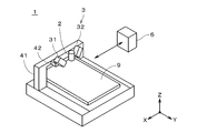
- FIG. 1 is a perspective view showing a crystallization index acquisition apparatus 1 according to an embodiment of the present invention.
- the crystallization index acquisition apparatus 1 is an apparatus that acquires a crystallization index indicating the degree of crystallization in a microcrystalline silicon film formed on a glass substrate 9 for a thin film silicon solar cell that is an object.
- the size of the glass substrate 9 is, for example, 1 to 2 m (meter) square.
- the crystallization index acquisition apparatus 1 includes an imaging unit 2 that images a glass substrate 9, a spectroscopic ellipsometer 3 for acquiring a measurement spectrum described later, a Y-direction moving unit 41 that can move in the Y direction in FIG.
- the computer 6 includes an X-direction moving unit 42 that can move in the X-direction, a CPU that performs various arithmetic processes, a memory that stores various types of information, and the like. It plays a role as a control unit for controlling the configuration.
- the X direction moving unit 42 is provided on the Y direction moving unit 41, and the imaging unit 2 and the spectroscopic ellipsometer 3 are fixed to the X direction moving unit 42.
- the light irradiation position by the spectroscopic ellipsometer 3 can be freely arranged at each position on the glass substrate 9.
- the spectroscopic ellipsometer 3 includes an illuminating unit 31 and a light receiving unit 32 arranged above the glass substrate 9 (on the (+ Z) side in FIG. 1), and is irradiated with polarized white light from the illuminating unit 31 toward the glass substrate 9. Then, the light receiving unit 32 receives the reflected light from the glass substrate 9.
- the light receiving unit 32 includes an analyzer that receives the reflected light and a spectroscope that acquires the spectral intensity of the reflected light. The rotational position of the analyzer and the spectral intensity of the reflected light acquired by the spectroscope are supplied to the computer 6. Is output.
- the phase difference between the p-polarized component and the s-polarized component and the reflection amplitude ratio angle are obtained as the polarization states of light having a plurality of frequencies (or wavelengths). That is, the frequency spectrum of the phase difference and the reflection amplitude ratio angle (hereinafter collectively referred to as “measurement spectrum”) is acquired.
- FIG. 2 is a diagram showing the configuration of the computer 6.
- the computer 6 has a general computer system configuration in which a CPU 61 that performs various arithmetic processes, a ROM 62 that stores basic programs, and a RAM 63 that stores various information are connected to a bus line.
- the bus line further includes a fixed disk 65 for storing information, a display 66 for displaying various information, a keyboard 67a and a mouse 67b for receiving input from an operator, an optical disk, a magnetic disk, a magneto-optical disk, and the like.
- a reading / writing device 68 that reads information from or writes information to the recording medium 60, and a communication unit 69 that communicates with the outside via an interface (I / F) as appropriate. Connected.
- the computer 6 reads the program 600 from the recording medium 60 via the reading / writing device 68 in advance and stores it in the fixed disk 65.
- the program 600 is copied to the RAM 63 and the CPU 61 executes arithmetic processing according to the program 600 in the RAM 63 (that is, when the computer executes the program), the computer 6 performs processing as an arithmetic unit described later. I do.
- FIG. 3 is a block diagram showing a functional configuration realized by the CPU 61, the ROM 62, the RAM 63, the fixed disk 65, and the like when the CPU 61 operates according to the program 600.
- the measurement dielectric function calculation unit 71 and the crystallization index calculation unit 73 of the calculation unit 7 are functions realized by the CPU 61 and the like
- the storage unit 72 is a function realized by the fixed disk 65 and the like.
- the function of the calculating part 7 may be implement
- a plurality of microcrystalline silicon films having different degrees of crystallization have conditions other than the ratio between the flow rate of monosilane and the flow rate of hydrogen (for example, the temperature at the time of film formation, the flow rate of other gases, and plasma generation). (Voltage) may be changed.
- FIG. 4 shows the dielectric function of these microcrystalline silicon films.
- the value of the hydrogen dilution rate R which is a value obtained by dividing the flow rate of hydrogen at the time of formation of the microcrystalline silicon film by the flow rate of monosilane, on the line indicating the imaginary part ⁇ 2 of the dielectric function of each microcrystalline silicon film.
- FIG. 4 the imaginary part of the dielectric function of the crystalline silicon film substantially having no amorphous component is also shown with the symbol “c-Si”.
- the dielectric function shown in FIG. 4 is obtained from the measured spectrum acquired by the spectroscopic ellipsometer 3, and is obtained without using the Tauc-Lorentz model or Harmonic model described later.
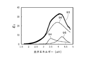
- a plurality of circles in FIG. 5 indicate a dielectric function (hereinafter referred to as “measurement dielectric function”) obtained from a spectrum measured by the spectroscopic ellipsometer 3, and a line 93 represents a theoretical dielectric function that models the dielectric function.
- the theoretical dielectric function 93 includes a partial dielectric function model 94 contributing to the low energy peak 91 (see FIG. 4), a partial dielectric function model 95 contributing to the high energy peak 92 (see FIG. 4), and the low energy peak 91 and high energy. This is expressed by synthesizing a partial dielectric function model 96 that models other than those that contribute to the energy peak 92.
- the partial dielectric function models 94 to 96 are referred to as “low energy peak model 94”, “high energy peak model 95”, and “background model 96”, respectively.
- the Tauc-Lorentz model is used as the low energy peak model 94 and the background model 96
- the Harmonic model is used as the high energy peak model 95.
- the theoretical dielectric function 93 matches the measured dielectric function with high accuracy. Therefore, it is understood that the dielectric function of the microcrystalline silicon film can be accurately expressed by synthesizing the low energy peak model 94, the high energy peak model 95, and the background model 96.
- the microcrystalline silicon film formed at the above hydrogen dilution rate R 20, 30, 50, 70, 100, respectively.
- the relationship between the parameters of the three partial dielectric function models (ie, the low energy peak model, the high energy peak model, and the background model) and the crystallization index ⁇ is stored in the storage unit 72 (see FIG. 3).
- or FIG. H is a graph showing the relationship between each parameter and the crystallization index ⁇ .
- or FIG. C represents the relationship between the band gap Eg, full width at half maximum C and amplitude A of the low energy peak model, and the crystallization index ⁇ , respectively.
- FIG. D shows the relationship between the full width at half maximum C of the high energy peak model and the crystallization index ⁇ .
- or FIG. H represents the relationship between the band gap Eg, the full width at half maximum C, the energy En at the peak position, the amplitude A, and the crystallization index ⁇ , respectively.
- each parameter of the parameter group is shown in FIG. A thru
- the amplitude of the high energy peak model is proportional to the crystallization index ⁇ as described above, and is not shown.
- each parameter is expressed as a function of the crystallization index ⁇ .
- the relationship between each parameter included in the theoretical dielectric function and the crystallization index ⁇ may be stored in the storage unit 72 in a tabular format, for example.
- FIG. 8 is a diagram showing a flow of processing for obtaining the crystallization index ⁇ of the microcrystalline silicon film on the glass substrate 9.
- the spectroscopic ellipsometer 3 places the glass substrate 9 on a predetermined position of the microcrystalline silicon film.
- a measurement spectrum is acquired by performing measurement on the surface (step S11).
- a measured dielectric function is obtained from the measured spectrum by the measured dielectric function computing unit 71 (see FIG. 3) of the computing unit 7 (step S12).
- the crystallization index calculation unit 73 calculates the value of the parameter group (that is, the parameters shown in FIGS. 7A to 7.H) included in the theoretical dielectric function of the microcrystalline silicon film, and The theoretical dielectric function is fitted to the measured dielectric function by changing the thickness value of the microcrystalline silicon film.
- the crystallization index ⁇ is changed during the fitting to be expressed by the crystallization index ⁇ (in the present embodiment, it is expressed as a function of the crystallization index ⁇ ).
- the value of each parameter in the parameter group is changed.
- the value of the crystallization index ⁇ and the thickness value at which the theoretical dielectric function is closest to the measured dielectric function are obtained (step S13).
- each parameter of the parameter group included in the theoretical dielectric function of the microcrystalline silicon film is expressed by the crystallization index ⁇ , and each crystallization index ⁇ is changed to change each parameter.
- the parameter value is changed to fit the theoretical dielectric function to the measured dielectric function.
- the crystallization index ⁇ of the microcrystalline silicon film can be easily and rapidly obtained as compared with the case where the fitting is performed by individually changing each parameter of the parameter group included in the theoretical dielectric function.
- a local solution may be obtained, but by expressing each parameter with a crystallization index ⁇ , the parameter can be prevented from taking a local solution. Fitting can be performed easily and accurately.
- the crystallization index ⁇ can be obtained with higher accuracy. Further, by changing the film thickness of the microcrystalline silicon film at the time of fitting, the film thickness can be easily and accurately obtained together with the crystallization index ⁇ . In addition, according to the request
- a plurality of partial dielectric function models that is, a low energy peak model, a high energy peak model, and a background model
- a crystallization index acquisition apparatus 1 a plurality of partial dielectric function models (that is, a low energy peak model, a high energy peak model, and a background model) used for the synthesis of a theoretical dielectric function by obtaining the crystallization index ⁇ .
- the crystallization index acquisition apparatus 1 it is not always necessary that all parameters of the parameter group included in the theoretical dielectric function are expressed by the crystallization index ⁇ .
- Each of the plurality of partial dielectric function models is represented by the crystallization index ⁇ . It is only necessary to include at least one parameter expressed by.
- all partial dielectric function models, each of which is a part of the theoretical dielectric function are expressed by the crystallization index ⁇ , so that the possibility that the parameter takes a local solution can be reduced. As a result, fitting can be performed easily and accurately.
- the microcrystalline silicon film By the way, in the microcrystalline silicon film, crystallization proceeds during the film forming process on the target, so that the portion near the target of the microcrystalline silicon film is closer to the crystal grain boundary than the portion far from the target. There are many crystal grain boundaries. Therefore, even if the film formation conditions such as the hydrogen dilution rate R are the same, the microcrystalline silicon film has a different dielectric function depending on the film thickness.
- the dielectric function in FIG. 9 is obtained from the spectrum measured by the spectroscopic ellipsometer 3.
- a line 81 and a line 82 indicate a real part ⁇ 1 and an imaginary part ⁇ 2 in the dielectric function of a microcrystalline silicon film having a thickness of 345 mm, respectively.
- a line 83 and a line 84 respectively show a real part ⁇ 1 and an imaginary part ⁇ 2 in the dielectric function of the microcrystalline silicon film having a thickness of 165 mm.
- the peak position of the dielectric function in the microcrystalline silicon film with a film thickness of 165 mm is almost the same as the peak position of the dielectric function in the microcrystalline silicon film with a film thickness of 345 mm in both the real part ⁇ 1 and imaginary part ⁇ 2.
- the amplitude of the dielectric function in the microcrystalline silicon film with a thickness of 165 mm is smaller than the amplitude of the dielectric function in the microcrystalline silicon film with a thickness of 345 mm. This is presumably because the number of crystal grain boundaries in the microcrystalline silicon film having a thickness of 165 mm is larger than that in the microcrystalline silicon film having a thickness of 345 mm.
- the increase / decrease in grain boundaries in the microcrystalline silicon film can be interpreted as the increase / decrease in voids in the microcrystalline silicon film.
- the volume fraction of voids assumed to be generated in the microcrystalline silicon film due to the grain boundary is fmSiC
- the dielectric function of the microcrystalline silicon film having a reference thickness of 345 mm is ⁇ ref
- the dielectric function ⁇ h of a microcrystalline silicon film having a thickness of 165 mm is considered to satisfy Equation 1 by the effective medium approximation.
- the f m SiC in Equation 1 is attributable to the volume fraction of voids assumed to be due to the presence of crystal grain boundaries in the microcrystalline silicon film having a thickness of 345 mm and the presence of crystal grain boundaries in the microcrystalline silicon film having a thickness of 165 mm. Then, it may be regarded as a difference from the assumed void volume fraction.
- the crystallization index acquisition apparatus 1 is necessary when the target for acquiring the crystallization index ⁇ is a relatively thin microcrystalline silicon film in the fitting by the crystallization index calculator 73 (see FIG. 3) in step S13 of FIG. Accordingly, the theory of the microcrystalline silicon film can be obtained by changing the volume fraction f mSiC using the effective medium theory (in this embodiment, effective medium approximation) including the void volume fraction f mSiC as a parameter. The amplitude of the dielectric function is changed.
- the microcrystalline silicon film having a thickness of 345 mm could be accurately fitted without using the effective medium theory.
- the fitting accuracy was lowered when the effective medium theory was not used, and the fitting could be performed with high accuracy by using the effective medium theory.
- the crystallization index ⁇ of the two types of microcrystalline silicon films is approximately equal, and the void volume fraction fmSiC in the microcrystalline silicon film having a thickness of 165 mm is 1 based on the microcrystalline silicon film having a thickness of 345 mm. It was 9%.
- the crystallization index acquisition apparatus 1 can accurately determine the crystallization index ⁇ by using the effective medium theory even when the microcrystalline silicon film is relatively thin. As a result, ellipsometry analysis of a relatively thin microcrystalline silicon film can be performed easily and with high accuracy.
- the microcrystalline silicon film 5 on the glass substrate 9 is first layer 51, second layer 52, Dividing into a plurality of layers of the third layer 53 and the fourth layer 54 (that is, assuming that the microcrystalline silicon film 5 is formed by laminating the plurality of layers in the film thickness direction), step S13 Fitting in is performed.
- step S13 Fitting in addition to the plurality of layers 51 to 54, minute unevenness (hereinafter referred to as “surface layer 55”) on the surface of the microcrystalline silicon film 5 is considered in the fitting.
- each of the first layer 51, the second layer 52, the third layer 53, and the fourth layer 54 is caused by the presence of crystal grain boundaries as in the above-described microcrystalline silicon film having a thickness of 165 mm. Then, using an effective medium theory that takes into account voids assumed to be generated in the microcrystalline silicon film, the crystallization index ⁇ , the film thickness, and the volume fraction of voids of each layer are changed.
- the effective medium theory is used, assuming that the microcrystalline silicon film having the same crystallization index ⁇ as that of the fourth layer 54 and the air layer exist by the same volume, and the crystallization index ⁇ and Change the film thickness. Then, while making these changes, fitting is performed between the synthetic theoretical dielectric function obtained by synthesizing the theoretical dielectric functions of the first layer 51 to the fourth layer 54 and the surface layer 55 and the measured dielectric function.
- Table 1 shows the crystallization index ⁇ , the film thickness, and the void volume fraction of each layer obtained by performing the above-described fitting on the microcrystalline silicon film 5 having a film thickness of about 800 mm.
- FIG. A and FIG. B is a diagram showing a polarization state of the microcrystalline silicon film 5.
- FIG. A and FIG. A plurality of circles in B indicate ⁇ and ⁇ (that is, measurement spectra) measured by the spectroscopic ellipsometer 3, and solid lines indicate theoretical spectra of ⁇ and ⁇ determined by the above-described fitting, respectively.
- the value of the crystallization index ⁇ is the smallest in the first layer 51 closest to the glass substrate 9 and increases as the distance from the glass substrate 9 increases. Further, the volume fraction of voids is largest in the first layer 51 closest to the glass substrate 9 and decreases as the distance from the glass substrate 9 increases. This is consistent with the property of the microcrystalline silicon film that crystallization proceeds during the film forming process on the object.
- the microcrystalline silicon film is divided into a plurality of layers in the film thickness direction, and the crystallization index ⁇ , the film thickness, and the volume fraction of voids are changed for each of the plurality of layers.
- the fitting may be performed with the film thickness of each layer fixed. Even in this case, the distribution of the crystallization index ⁇ of the relatively thick film can be obtained with high accuracy.
- the number of divisions in the film thickness direction of the microcrystalline silicon film may be changed as appropriate. Further, when the influence of the surface layer 55 is relatively small, the surface layer 55 may not be considered.
- each parameter of the parameter group included in the theoretical dielectric function of each layer obtained by dividing the microcrystalline silicon film is expressed by the crystallization index ⁇ of each layer, and the crystallization index ⁇ is changed.
- the value of each parameter is changed to fit the theoretical dielectric function to the measured dielectric function.
- a model different from the above embodiment may be used as the low energy peak model, the high energy peak model, and the background model.
- a Tauc-Lorentz model may be used as the high energy peak model.
- the parameters of the partial dielectric function model other than the parameters indicated by H are expressed by the crystallization index ⁇ , and may be changed along with the change of the crystallization index ⁇ when fitting the theoretical dielectric function to the measured dielectric function.
- the theoretical dielectric function is not necessarily expressed by synthesizing the low energy peak model, the high energy peak model, and the background model, and a plurality of partial dielectrics including the high energy peak model. It may be expressed by synthesizing a function model. Also for the parameter group whose value is changed during fitting, it is not necessary that all parameters of the parameter group are expressed by the crystallization index ⁇ , the amplitude of the high energy peak model included in the parameter group, and the above It is sufficient that at least one parameter of another partial dielectric function model included in the plurality of partial dielectric function models is expressed by the crystallization index ⁇ . Thereby, the crystallization index ⁇ of the microcrystalline silicon film can be obtained easily and accurately.
- the crystallization index acquisition apparatus 1 can acquire the crystallization index ⁇ of a microcrystalline silicon film formed on various objects such as a substrate for a solar cell other than the glass substrate 9 and a plastic film. .
- the microcrystalline silicon film may be formed by a method other than the CVD method.
Landscapes
- Physics & Mathematics (AREA)
- Health & Medical Sciences (AREA)
- Life Sciences & Earth Sciences (AREA)
- Chemical & Material Sciences (AREA)
- Analytical Chemistry (AREA)
- Biochemistry (AREA)
- General Health & Medical Sciences (AREA)
- General Physics & Mathematics (AREA)
- Immunology (AREA)
- Pathology (AREA)
- Investigating Or Analysing Materials By Optical Means (AREA)
- Crystals, And After-Treatments Of Crystals (AREA)
- Testing Or Measuring Of Semiconductors Or The Like (AREA)
Abstract
結晶化指数取得装置(1)では、微結晶シリコン膜(5)の理論誘電関数(93)を複数の部分誘電関数モデルの合成として表現し、微結晶シリコン膜(5)における結晶化の程度を示す結晶化指数κが、複数の部分誘電関数モデルのうち、結晶シリコン膜の誘電関数における虚部の高エネルギー側のピーク(92)に寄与する高エネルギーピークモデル(95)の振幅に基づいて設定される。そして、複数の部分誘電関数モデルに含まれるパラメータ群の各パラメータを結晶化指数κにより表現し、結晶化指数κを変更することにより各パラメータの値を変更し、分光エリプソメータ(3)により取得された測定誘電関数に対する理論誘電関数(93)のフィッティングが行われる。これにより、微結晶シリコン膜(5)の結晶化指数κを容易かつ精度良く求めることができる。
Description
本発明は、対象物上に形成された微結晶シリコン膜における結晶化の程度を示す結晶化指数を取得する技術に関する。
近年、地球環境問題への注目の高まりにより、クリーンな太陽光を利用する太陽電池の開発が行われており、特に、大面積化および低コスト化が可能な薄膜シリコン太陽電池が次世代の太陽電池として注目されている。薄膜シリコン太陽電池の製造では、CVD(Chemical Vapor Deposition)法等によりガラス基板上にシリコン膜が形成される。シリコン膜としては、アモルファスシリコン膜や、アモルファス成分と結晶成分とが混在する微結晶シリコン膜等が利用される。
特開平11-317433号公報は、多結晶半導体膜の結晶粒子の粒径を測定する技術に関する。特開平11-317433号公報の検査方法では、評価対象の多結晶半導体薄膜(評価試料)の誘電率が、分光エリプソメータによる測定結果に基づいて求められる。そして、評価試料の誘電率が、平均粒径が既知の複数種類の多結晶半導体薄膜(標準試料)の誘電率と比較され、これにより算出された誘電率のピーク値の半値全幅との相関を取ることにより、評価試料の粒径が求められる。
ところで、微結晶シリコン膜では、アモルファス成分と結晶成分との混在により、誘電関数が複雑になる。また、微結晶シリコン膜は、成膜の際に、膜厚の増加に従って結晶化の程度(すなわち、アモルファス成分と結晶成分の割合)が変化する。このため、微結晶シリコン膜のエリプソメトリー解析を行う際に、結晶化の程度を精度良く求めつつ解析を行おうとすると、解析すべきパラメータ数が非常に多くなってしまい、微結晶シリコン膜の光学特性を精度良く求めることが困難である。例えば、特開平11-317433号公報では、多結晶半導体薄膜の誘電率のピーク値に注目して結晶粒子の粒径を求めることが提案されているが、誘電率のピーク値以外の部分を無視することになるため、粒径の算出精度を向上することに限界がある。
また、微結晶シリコン膜における結晶化の程度を非破壊にて測定する方法としては、ラマン分光法が知られている。しかしながら、ラマン分光法では、測定に使用するレーザ光の波長によって測定可能な膜厚が決定されるため、微結晶シリコン膜のように膜厚方向で結晶化の程度が変化する場合であっても、膜厚方向において均一であるものと仮定された結晶化の程度を求めることになる。また、測定対象の膜厚が、測定可能な所定の膜厚よりも厚い場合や薄い場合、結晶化の程度を正しく求めることができない。さらに、ラマン分光法では、膜厚を測定することができない。
本発明は、対象物上に形成された微結晶シリコン膜における結晶化の程度を示す結晶化指数を取得する結晶化指数取得装置に向けられており、結晶化指数を容易かつ精度良く取得することを目的としている。
本発明に係る結晶化指数取得装置は、分光エリプソメータと、前記分光エリプソメータにて対象物上の微結晶シリコン膜に対して測定を行うことにより取得された測定スペクトルから測定誘電関数を求め、前記微結晶シリコン膜の理論誘電関数に含まれるパラメータ群の値を変更して前記理論誘電関数の前記測定誘電関数に対するフィッティングを行うことにより、結晶化指数を求める演算部とを備え、前記理論誘電関数が、結晶シリコン膜の誘電関数における虚部の2つのピークのうち高エネルギー側のピークに寄与する高エネルギーピークモデルを含む複数の部分誘電関数モデルを合成することにより表現され、前記パラメータ群に前記高エネルギーピークモデルの振幅が含まれ、前記振幅が前記結晶化指数にて表現され、他の部分誘電関数モデルの少なくとも1つのパラメータも前記結晶化指数にて表現され、前記フィッティングの際に、前記結晶化指数が変更されることにより、前記結晶化指数にて表現されるパラメータが変更される。結晶化指数取得装置では、結晶化指数を容易かつ精度良く取得することができる。
好ましくは、前記演算部において、前記フィッティングの際に前記微結晶シリコン膜の膜厚も変更され、前記結晶化指数と共に前記膜厚も求められる。
他の好ましい実施の形態では、前記複数の部分誘電関数モデルのそれぞれが、前記結晶化指数にて表現される少なくとも1つのパラメータを含む。より好ましくは、前記パラメータ群の各パラメータが、前記結晶化指数にて表現される。
他の好ましい実施の形態では、前記演算部が、前記フィッティングにおいて、微結晶シリコン膜中に生じると仮定したボイドの体積分率をパラメータとして含む有効媒質理論を用い、前記体積分率を変更することにより、前記理論誘電関数の振幅を変更する。より好ましくは、前記演算部により、微結晶シリコン膜を膜厚方向において複数の層に分割し、前記複数の層のそれぞれについて、前記結晶化指数および前記体積分率を変更して前記フィッティングが行われる。
本発明は、また、対象物上に形成された微結晶シリコン膜における結晶化の程度を示す結晶化指数を取得する結晶化指数取得方法にも向けられている。前記結晶化指数取得方法は、a)分光エリプソメータにて対象物上の微結晶シリコン膜に対して測定を行うことにより測定スペクトルを取得し、前記測定スペクトルから測定誘電関数を求める工程と、b)前記微結晶シリコン膜の理論誘電関数に含まれるパラメータ群の値を変更して前記理論誘電関数の前記測定誘電関数に対するフィッティングを行うことにより、結晶化指数を求める工程とを備え、前記理論誘電関数が、結晶シリコン膜の誘電関数における虚部の2つのピークのうち高エネルギー側のピークに寄与する高エネルギーピークモデルを含む複数の部分誘電関数モデルを合成することにより表現され、前記パラメータ群に前記高エネルギーピークモデルの振幅が含まれ、前記振幅が前記結晶化指数にて表現され、他の部分誘電関数モデルの少なくとも1つのパラメータも前記結晶化指数にて表現され、前記フィッティングの際に、前記結晶化指数が変更されることにより、前記結晶化指数にて表現されるパラメータが変更される。
上述の目的および他の目的、特徴、態様および利点は、添付した図面を参照して以下に行うこの発明の詳細な説明により明らかにされる。
図1は、本発明の一の実施の形態に係る結晶化指数取得装置1を示す斜視図である。結晶化指数取得装置1は、対象物である薄膜シリコン太陽電池用のガラス基板9上に形成された微結晶シリコン膜中における結晶化の程度を示す結晶化指数を取得する装置である。ガラス基板9のサイズは、例えば1~2m(メートル)角である。
結晶化指数取得装置1は、ガラス基板9上を撮像する撮像部2、後述の測定スペクトルを取得するための分光エリプソメータ3、図1中のY方向に移動可能なY方向移動部41、図1中のX方向に移動可能なX方向移動部42、並びに、各種演算処理を行うCPUや各種情報を記憶するメモリ等により構成されたコンピュータ6を備え、コンピュータ6は結晶化指数取得装置1の各構成を制御する制御部としての役割を果たす。X方向移動部42はY方向移動部41上に設けられ、X方向移動部42には、撮像部2および分光エリプソメータ3が固定される。結晶化指数取得装置1では、分光エリプソメータ3による光の照射位置をガラス基板9上の各位置に自在に配置することが可能となっている。
分光エリプソメータ3は、ガラス基板9の上方(図1中の(+Z)側)に配置される照明部31および受光部32を備え、照明部31からガラス基板9に向けて偏光した白色光が照射され、受光部32にてガラス基板9からの反射光が受光される。受光部32は、反射光が入射する検光子および反射光の分光強度を取得する分光器を有し、検光子の回転位置、および、分光器により取得された反射光の分光強度がコンピュータ6へと出力される。コンピュータ6では、複数の振動数(または、波長)の光のそれぞれの偏光状態として、p偏光成分とs偏光成分との位相差および反射振幅比角が求められる。すなわち、位相差および反射振幅比角の振動数スペクトル(以下、「測定スペクトル」と総称する。)が取得される。
図2は、コンピュータ6の構成を示す図である。コンピュータ6は、各種演算処理を行うCPU61、基本プログラムを記憶するROM62および各種情報を記憶するRAM63をバスラインに接続した一般的なコンピュータシステムの構成となっている。バスラインにはさらに、情報記憶を行う固定ディスク65、各種情報の表示を行うディスプレイ66、操作者からの入力を受け付けるキーボード67aおよびマウス67b、光ディスク、磁気ディスク、光磁気ディスク等のコンピュータ読み取り可能な記録媒体60から情報の読み取りを行ったり記録媒体60に情報の書き込みを行う読取/書込装置68、並びに、外部との通信を行う通信部69が、適宜、インターフェイス(I/F)を介する等して接続される。
コンピュータ6には、事前に読取/書込装置68を介して記録媒体60からプログラム600が読み出され、固定ディスク65に記憶される。そして、プログラム600がRAM63にコピーされるとともにCPU61がRAM63内のプログラム600に従って演算処理を実行することにより(すなわち、コンピュータがプログラムを実行することにより)、コンピュータ6が、後述の演算部としての処理を行う。
図3は、CPU61がプログラム600に従って動作することにより、CPU61、ROM62、RAM63、固定ディスク65等が実現する機能構成を示すブロック図である。図3において、演算部7の測定誘電関数演算部71および結晶化指数演算部73がCPU61等により実現される機能であり、記憶部72が固定ディスク65等により実現される機能である。なお、演算部7の機能は専用の電気的回路により実現されてもよく、部分的に電気的回路が用いられてもよい。
次に、結晶化指数取得装置1における結晶化指数の測定原理について述べる。ここでは、CVD工程において、原料ガスであるモノシラン(SiH4)の流量と水素(H2)の流量との割合を変更しつつ、複数のシリコン基板上に微結晶シリコン膜を順次形成することにより、結晶化の程度が互いに異なる複数の微結晶シリコン膜が準備されているものとする。そして、これらの微結晶シリコン膜について、結晶化指数取得装置1の分光エリプソメータ3にて取得された測定スペクトルから誘電関数が求められる。なお、結晶化の程度が異なる複数の微結晶シリコン膜は、モノシランの流量と水素の流量との割合以外の条件(例えば、成膜時の温度や他のガスの流量、プラズマを発生させるための電圧)を変更することにより作製されてもよい。
図4は、これらの微結晶シリコン膜の誘電関数を示す図である。誘電関数εは、実部であるε1と虚部であるε2とを含む複素関数にて表現され(すなわち、虚数単位をiとして(ε=ε1+iε2))、図4の縦軸は誘電関数の虚部ε2を示し、横軸は振動数に対応する光子エネルギーを示している。図4では、各微結晶シリコン膜の誘電関数の虚部ε2を示す線に、当該微結晶シリコン膜の形成時における水素の流量をモノシランの流量で割った値である水素希釈率Rの値(R=10,30,50,100)を付している。また、図4では、アモルファス成分を実質的に有しない結晶シリコン膜の誘電関数の虚部も、「c-Si」の符号を付して共に示す。なお、図4の誘電関数は、分光エリプソメータ3にて取得された測定スペクトルから求められたものであり、後述するTauc-LorentzモデルやHarmonicモデルを用いることなく求めたものである。
図4に示す誘電関数のうち、R=10の誘電関数では、結晶シリコン膜の誘電関数における虚部の2つのピーク91,92に対応する成分はほとんど存在しないが、R=30,50,100の各誘電関数では、低エネルギー側のピーク91および高エネルギー側のピーク92(以下、「低エネルギーピーク91」および「高エネルギーピーク92」という。)に対応する変化が、光子エネルギーが3.4eVおよび4.25eVの近傍に存在する。これは、成膜時の水素希釈率Rが大きい微結晶シリコン膜では、膜中の結晶成分の割合が増大し、結晶成分に起因するピーク91,92の影響が顕在化することによるものと考えられる。
図5は、R=50の微結晶シリコン膜の誘電関数を解析した結果を示すものである。図5中の複数の丸印は、分光エリプソメータ3による測定スペクトルから求められた誘電関数(以下、「測定誘電関数」という。)を示し、線93は、誘電関数をモデル化した理論誘電関数を示す。理論誘電関数93は、低エネルギーピーク91(図4参照)に寄与する部分誘電関数モデル94、高エネルギーピーク92(図4参照)に寄与する部分誘電関数モデル95、並びに、低エネルギーピーク91および高エネルギーピーク92に寄与するもの以外をモデル化した部分誘電関数モデル96を合成することにより表現される。
以下の説明では、部分誘電関数モデル94~96をそれぞれ、「低エネルギーピークモデル94」、「高エネルギーピークモデル95」および「バックグラウンドモデル96」という。本実施の形態では、低エネルギーピークモデル94およびバックグラウンドモデル96として、Tauc-Lorentzモデルを用い、高エネルギーピークモデル95として、Harmonicモデルが用いられる。
図5に示すように、理論誘電関数93は、測定誘電関数に精度良く一致している。したがって、低エネルギーピークモデル94、高エネルギーピークモデル95およびバックグラウンドモデル96を合成することにより、微結晶シリコン膜の誘電関数を精度良く表現できることが理解される。
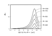
ここで、上記3つの部分誘電関数モデルのうち、高エネルギーピークモデルに注目する。図6は、水素希釈率R=20,30,70,100にてそれぞれ成膜された微結晶シリコン膜について、図5に示すR=50の微結晶シリコン膜と同様に解析し、得られた3つの部分誘電関数モデルのうち高エネルギーピークモデルを図示したものである。図6では、図5に示すR=50の微結晶シリコン膜の高エネルギーピークモデルも共に示す。また、図6では、各微結晶シリコン膜の高エネルギーピークモデルを示す線に、各微結晶シリコン膜の形成時における水素希釈率Rの値を付している。
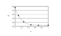
図6に示すように、高エネルギーピークモデルの振幅は、水素希釈率Rが大きくなるに従って、すなわち、微結晶シリコン膜中の結晶成分の割合が増大するに従って漸次増大する。そこで、微結晶シリコン膜における結晶化の程度を示す結晶化指数κを、R=100の高エネルギーピークモデルの振幅に対する各Rの高エネルギーピークモデルの振幅の割合として設定する。具体的には、R=100のときに結晶化指数κは1となり、Rが小さくなるに従ってκも小さくなり、R=0のときにκも0となる。高エネルギーピークモデルの振幅は、結晶化指数κに正比例する。
結晶化指数取得装置1では、測定対象となる微結晶シリコン膜の測定の事前処理として、上述の水素希釈率R=20,30,50,70,100にてそれぞれ成膜された微結晶シリコン膜の3つの部分誘電関数モデル(すなわち、低エネルギーピークモデル、高エネルギーピークモデルおよびバックグラウンドモデル)のパラメータと、結晶化指数κとの関係が、記憶部72(図3参照)に記憶される。
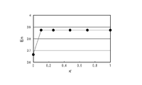
図7.Aないし図7.Hはそれぞれ、各パラメータと結晶化指数κとの関係を示す図である。図7.Aないし図7.Cはそれぞれ、低エネルギーピークモデルのバンドギャップEg、半値全幅Cおよび振幅Aと結晶化指数κとの関係を示す。図7.Dは、高エネルギーピークモデルの半値全幅Cと結晶化指数κとの関係を示す。図7.Eないし図7.Hはそれぞれ、バックグラウンドモデルのバンドギャップEg、半値全幅C、ピーク位置のエネルギーEnおよび振幅Aと結晶化指数κとの関係を示す。
結晶化指数取得装置1では、これらのパラメータ、および、結晶化指数κの設定基準である高エネルギーピークモデルの振幅が、後述するフィッティングの際に値が変更される理論誘電関数のパラメータ群となる。パラメータ群の各パラメータは、図7.Aないし図7.Hに示す関係にて、結晶化指数κにて表現される。なお、高エネルギーピークモデルの振幅は、上述のように結晶化指数κに比例しており、図示は省略する。本実施の形態では、各パラメータが、結晶化指数κの関数として表現される。図7.Aないし図7.Hでは、記憶部72に記憶される上記関数を実線にて示す。理論誘電関数に含まれる各パラメータと結晶化指数κとの関係は、例えば、表形式にて記憶部72に記憶されてもよい。
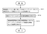
図8は、ガラス基板9上の微結晶シリコン膜の結晶化指数κを取得する処理の流れを示す図である。結晶化指数取得装置1では、結晶化指数κが未知の微結晶シリコン膜が設けられたガラス基板9が搬入されると、分光エリプソメータ3にてガラス基板9上の微結晶シリコン膜の所定位置に対して測定を行うことにより測定スペクトルが取得される(ステップS11)。続いて、演算部7の測定誘電関数演算部71(図3参照)により、上記測定スペクトルから測定誘電関数が求められる(ステップS12)。
次に、結晶化指数演算部73(図3参照)により、微結晶シリコン膜の理論誘電関数に含まれる上記パラメータ群(すなわち、図7.Aないし図7.Hに示すパラメータ)の値、および、微結晶シリコン膜の膜厚の値を変更して、理論誘電関数の測定誘電関数に対するフィッティングが行われる。結晶化指数取得装置1では、当該フィッティングの際に、結晶化指数κが変更されることにより、結晶化指数κにより表現される(本実施の形態では、結晶化指数κの関数として表現される)上記パラメータ群の各パラメータの値が変更される。そして、理論誘電関数が測定誘電関数に最も近くなる結晶化指数κの値および膜厚の値が求められる(ステップS13)。
以上に説明したように、結晶化指数取得装置1では、微結晶シリコン膜の理論誘電関数に含まれるパラメータ群の各パラメータを結晶化指数κにより表現し、結晶化指数κを変更することにより各パラメータの値を変更して理論誘電関数の測定誘電関数に対するフィッティングが行われる。これにより、理論誘電関数に含まれるパラメータ群の各パラメータを個別に変更してフィッティングを行う場合に比べて、微結晶シリコン膜の結晶化指数κを容易かつ迅速に求めることができる。また、上記各パラメータを個別に変更する場合、局所解を求めてしまうおそれがあるが、各パラメータを結晶化指数κにて表現することにより、パラメータが局所解を取ることを防止することができ、フィッティングを容易かつ精度良く行うことができる。
さらに、上述のように、理論誘電関数全体を測定誘電関数全体に対してフィッティングすることにより、理論誘電関数の一部の値(例えば、ピーク値)のみを測定誘電関数の対応する値に合わせる場合に比べて、結晶化指数κをより精度良く求めることができる。また、フィッティングの際に微結晶シリコン膜の膜厚も変更されることにより、当該膜厚も結晶化指数κと共に容易かつ精度良く求めることができる。なお、結晶化指数取得装置1の使用者の要求に応じて、求められた結晶化指数κおよび膜厚のうち、膜厚のみが出力されてもよい。
結晶化指数取得装置1では、結晶化指数κが求められることにより、理論誘電関数の合成に利用される複数の部分誘電関数モデル(すなわち、低エネルギーピークモデル、高エネルギーピークモデルおよびバックグラウンドモデル)の各パラメータも精度良く求められ、高精度な理論誘電関数を得ることができる。その結果、微結晶シリコン膜のエリプソメトリー解析を容易かつ高精度に行うことが可能となる。
結晶化指数取得装置1では、必ずしも、理論誘電関数に含まれるパラメータ群の全てのパラメータが結晶化指数κにて表現される必要はなく、複数の部分誘電関数モデルのそれぞれが、結晶化指数κにて表現される少なくとも1つのパラメータを含んでいればよい。これにより、それぞれが理論誘電関数の一部である全ての部分誘電関数モデルが結晶化指数κにより表現されることになるため、パラメータが局所解を取る可能性を低減することができる。その結果、フィッティングを容易かつ精度良く行うことができる。
ところで、微結晶シリコン膜では、対象物上における成膜工程中に結晶化が進行するため、微結晶シリコン膜の対象物に近い部位では、対象物から遠い部位に比べて、結晶粒の境界である結晶粒界が多くなる。このため、水素希釈率R等の成膜条件が同じであっても、微結晶シリコン膜は、その膜厚によって誘電関数が異なる。
図9は、水素希釈率R=50にて成膜された膜厚345Å(オングストローム)の微結晶シリコン膜、および、膜厚165Åの微結晶シリコン膜の誘電関数を示す図である。図9中の誘電関数は、分光エリプソメータ3による測定スペクトルから求められたものである。線81および線82はそれぞれ、膜厚345Åの微結晶シリコン膜の誘電関数における実部ε1および虚部ε2を示す。線83および線84はそれぞれ、膜厚165Åの微結晶シリコン膜の誘電関数における実部ε1および虚部ε2を示す。
図9に示すように、膜厚165Åの微結晶シリコン膜における誘電関数のピーク位置は、実部ε1および虚部ε2共に、膜厚345Åの微結晶シリコン膜における誘電関数のピーク位置とほぼ一致しており、膜厚165Åの微結晶シリコン膜における誘電関数の振幅は、膜厚345Åの微結晶シリコン膜における誘電関数の振幅に比べて小さい。これは、膜厚165Åの微結晶シリコン膜中の結晶粒界が、膜厚345Åの微結晶シリコン膜に比べて多いことに起因すると考えられる。微結晶シリコン膜中の結晶粒界の増減は、微結晶シリコン膜中のボイドの増減と解釈することができる。
そこで、結晶粒界に起因して微結晶シリコン膜中に生じると仮定したボイドの体積分率をfmSiC、基準とする膜厚345Åの微結晶シリコン膜の誘電関数をεref、真空の誘電関数をεbとして、膜厚165Åの微結晶シリコン膜の誘電関数εhは、有効媒質近似により数1を満たすとものと考える。

数1中のfmSiCは、膜厚345Åの微結晶シリコン膜における結晶粒界の存在に起因すると仮定したボイドの体積分率と、膜厚165Åの微結晶シリコン膜における結晶粒界の存在に起因すると仮定したボイドの体積分率との差と捉えられてもよい。
結晶化指数取得装置1では、図8のステップS13における結晶化指数演算部73(図3参照)によるフィッティングにおいて、結晶化指数κを取得する対象が比較的薄い微結晶シリコン膜の場合等、必要に応じて、上記ボイドの体積分率fmSiCをパラメータとして含む有効媒質理論(本実施の形態では、有効媒質近似)を用い、体積分率fmSiCを変更することにより、微結晶シリコン膜の理論誘電関数の振幅が変更される。
上述の膜厚が異なる2種類の微結晶シリコン膜を例に取ると、膜厚345Åの微結晶シリコン膜については、上記有効媒質理論を用いることなく、精度良くフィッティングを行うことができた。また、膜厚165Åの微結晶シリコン膜については、有効媒質理論を用いない場合は、フィッティングの精度が低下し、上記有効媒質理論を用いることにより、精度良くフィッティングを行うことができた。その結果、2種類の微結晶シリコン膜の結晶化指数κはおよそ等しくなり、膜厚165Åの微結晶シリコン膜におけるボイドの体積分率fmSiCは、膜厚345Åの微結晶シリコン膜を基準として、1.9%となった。このように、結晶化指数取得装置1では、微結晶シリコン膜が比較的薄い場合であっても、有効媒質理論を用いることにより、結晶化指数κを精度良く求めることができる。その結果、比較的薄い微結晶シリコン膜のエリプソメトリー解析を容易かつ高精度に行うことが可能となる。
次に、微結晶シリコン膜が比較的厚い場合の結晶化指数κの算出について説明する。上述のように、微結晶シリコン膜では、対象物上における成膜工程中に結晶化が進行するため、微結晶シリコン膜の対象物に近い部位では、対象物から遠い部位に比べて、結晶粒の境界である結晶粒界が多くなり、ボイドの体積分率fmSiCも大きくなる。また、微結晶シリコン膜が比較的厚い場合、微結晶シリコン膜の対象物に近い部位は、対象物から遠い部位に比べて結晶化指数κが小さくなる。
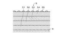
そこで、結晶化指数演算部73では、図10に示すように、ガラス基板9上の微結晶シリコン膜5を、膜厚方向においてガラス基板9に近い方から第1層51、第2層52、第3層53および第4層54の複数の層に分割して(すなわち、微結晶シリコン膜5は、当該複数の層が膜厚方向に積層されたものであると仮定して)、ステップS13におけるフィッティングが行われる。本実施の形態では、当該フィッティングにおいて、上記複数の層51~54に加えて、微結晶シリコン膜5の表面の微小な凹凸(以下、「表面層55」という。)についても考慮する。
具体的には、第1層51、第2層52、第3層53および第4層54のそれぞれについて、上述の膜厚165Åの微結晶シリコン膜と同様に、結晶粒界の存在に起因して微結晶シリコン膜中に生じると仮定したボイドを考慮する有効媒質理論を用い、各層の結晶化指数κ、膜厚およびボイドの体積分率をそれぞれ変更する。また、表面層55については、第4層54と同様の結晶化指数κを有する微結晶シリコン膜と空気の層とが同体積ずつ存在すると仮定して有効媒質理論を用い、結晶化指数κおよび膜厚をそれぞれ変更する。そして、これらの変更を行いつつ、第1層51~第4層54、および、表面層55の理論誘電関数を合成した合成理論誘電関数と、測定誘電関数とのフィッティングが行われる。
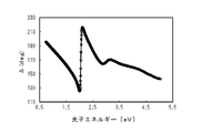
表1は、膜厚約800Åの微結晶シリコン膜5について上述のフィッティングを行って求められた各層の結晶化指数κ、膜厚およびボイドの体積分率を示す。また、図11.Aおよび図11.Bはそれぞれ、微結晶シリコン膜5の偏光状態を示す図である。図11.Aおよび図11.B中の複数の丸印は、分光エリプソメータ3により測定されたΨおよびΔ(すなわち、測定スペクトル)を示し、実線はそれぞれ、上述のフィッティングにより求められたΨおよびΔの理論スペクトルを示す。
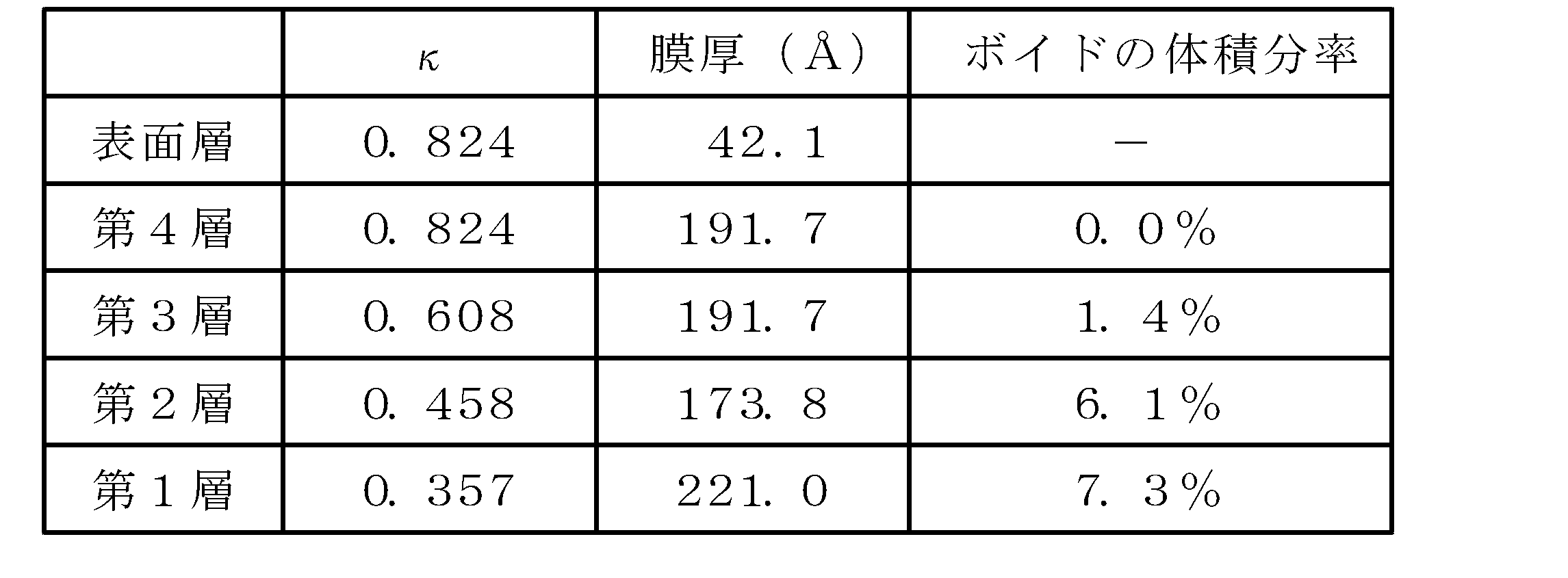
表1に示すように、結晶化指数κの値は、ガラス基板9に最も近い第1層51が最も小さく、ガラス基板9から離れるに従って大きくなる。また、ボイドの体積分率は、ガラス基板9に最も近い第1層51が最も大きく、ガラス基板9から離れるに従って小さくなる。これは、対象物上における成膜工程中に結晶化が進行するという微結晶シリコン膜の性質に合致している。また、図11.Aおよび図11.Bに示すように、結晶化指数演算部73により求められた微結晶シリコン膜5の偏光状態に関する理論スペクトルは、分光エリプソメータ3による測定スペクトルに精度良く一致している。
このように、結晶化指数取得装置1では、微結晶シリコン膜を膜厚方向において複数の層に分割し、複数の層のそれぞれについて、結晶化指数κ、膜厚およびボイドの体積分率を変更してフィッティングが行われることにより、比較的厚い膜の結晶化指数κの分布および膜厚を、精度良く求めることができる。結晶化指数取得装置1では、当該フィッティングは、各層の膜厚を固定して行われてもよい。この場合であっても、比較的厚い膜の結晶化指数κの分布を精度良く求めることができる。なお、微結晶シリコン膜の膜厚方向における分割数は、適宜変更されてよい。また、表面層55による影響が比較的小さい場合には、表面層55については考慮しなくてもよい。
ところで、比較的厚い微結晶シリコン膜の解析を行う場合、微結晶シリコン膜の各層において、理論誘電関数に含まれるパラメータ群の各パラメータを個別に変更してフィッティングを行おうとすると、パラメータ数が非常に多くなってしまい、結晶化指数κの算出に多大な時間を要したり、パラメータが局所解を取ってしまうおそれがある。これに対し、結晶化指数取得装置1では、微結晶シリコン膜を分割した各層の理論誘電関数に含まれるパラメータ群の各パラメータを、各層の結晶化指数κにより表現し、結晶化指数κを変更することにより各パラメータの値を変更して理論誘電関数の測定誘電関数に対するフィッティングが行われる。これにより、比較的厚い微結晶シリコン膜の結晶化指数κを容易かつ迅速に求めることができる。その結果、比較的厚い微結晶シリコン膜のエリプソメトリー解析を容易かつ高精度に行うことが可能となる。
以上、本発明の実施の形態について説明してきたが、本発明は上記実施の形態に限定されるものではなく、様々な変更が可能である。
例えば、低エネルギーピークモデル、高エネルギーピークモデルおよびバックグラウンドモデルとして、上記実施の形態とは異なるモデルが用いられてもよい。例えば、高エネルギーピークモデルとして、Tauc-Lorentzモデルが用いられてもよい。
結晶化指数取得装置1では、図7.Aないし図7.Hに示すパラメータ以外の部分誘電関数モデルのパラメータが、結晶化指数κにより表現され、理論誘電関数の測定誘電関数に対するフィッティングの際に、結晶化指数κの変更に伴って変更されてよい。
結晶化指数取得装置1では、理論誘電関数は、必ずしも、低エネルギーピークモデル、高エネルギーピークモデルおよびバックグラウンドモデルを合成することにより表現される必要はなく、高エネルギーピークモデルを含む複数の部分誘電関数モデルを合成することにより表現されていればよい。フィッティングの際に値が変更されるパラメータ群についても、パラメータ群の全てのパラメータが結晶化指数κにて表現される必要はなく、当該パラメータ群に含まれる高エネルギーピークモデルの振幅、および、上記複数の部分誘電関数モデルに含まれる他の部分誘電関数モデルの少なくとも1つのパラメータが結晶化指数κにて表現されていればよい。これにより、微結晶シリコン膜の結晶化指数κを容易かつ精度良く取得することができる。
結晶化指数取得装置1では、ガラス基板9以外の太陽電池用の基板や、プラスチックフィルム等、様々な対象物上に形成された微結晶シリコン膜の結晶化指数κを取得することが可能である。また、微結晶シリコン膜は、CVD法以外の手法にて形成されたものであってよい。
発明を詳細に描写して説明したが、既述の説明は例示的であって限定的なものではない。したがって、本発明の範囲を逸脱しない限り、多数の変形や態様が可能であるといえる。
1 結晶化指数取得装置
3 分光エリプソメータ
5 微結晶シリコン膜
7 演算部
9 ガラス基板
51 第1層
52 第2層
53 第3層
54 第4層
55 表面層
91 低エネルギーピーク
92 高エネルギーピーク
93 理論誘電関数
94 低エネルギーピークモデル
95 高エネルギーピークモデル
96 バックグラウンドモデル
S11~S13 ステップ
3 分光エリプソメータ
5 微結晶シリコン膜
7 演算部
9 ガラス基板
51 第1層
52 第2層
53 第3層
54 第4層
55 表面層
91 低エネルギーピーク
92 高エネルギーピーク
93 理論誘電関数
94 低エネルギーピークモデル
95 高エネルギーピークモデル
96 バックグラウンドモデル
S11~S13 ステップ
Claims (14)
- 対象物(9)上に形成された微結晶シリコン膜(5)における結晶化の程度を示す結晶化指数を取得する結晶化指数取得装置(1)であって、
分光エリプソメータ(3)と、
前記分光エリプソメータ(3)にて対象物(9)上の微結晶シリコン膜(5)に対して測定を行うことにより取得された測定スペクトルから測定誘電関数を求め、前記微結晶シリコン膜(5)の理論誘電関数(93)に含まれるパラメータ群の値を変更して前記理論誘電関数(93)の前記測定誘電関数に対するフィッティングを行うことにより、結晶化指数を求める演算部と、
を備え、
前記理論誘電関数(93)が、結晶シリコン膜の誘電関数における虚部の2つのピーク(91,92)のうち高エネルギー側のピーク(92)に寄与する高エネルギーピークモデル(95)を含む複数の部分誘電関数モデルを合成することにより表現され、
前記パラメータ群に前記高エネルギーピークモデル(95)の振幅が含まれ、前記振幅が前記結晶化指数にて表現され、他の部分誘電関数モデルの少なくとも1つのパラメータも前記結晶化指数にて表現され、
前記フィッティングの際に、前記結晶化指数が変更されることにより、前記結晶化指数にて表現されるパラメータが変更される。 - 請求項1に記載の結晶化指数取得装置(1)であって、
前記演算部において、前記フィッティングの際に前記微結晶シリコン膜(5)の膜厚も変更され、前記結晶化指数と共に前記膜厚も求められる。 - 請求項1または2に記載の結晶化指数取得装置(1)であって、
前記複数の部分誘電関数モデルのそれぞれが、前記結晶化指数にて表現される少なくとも1つのパラメータを含む。 - 請求項3に記載の結晶化指数取得装置(1)であって、
前記パラメータ群の各パラメータが、前記結晶化指数にて表現される。 - 請求項1ないし4のいずれかに記載の結晶化指数取得装置(1)であって、
前記演算部が、前記フィッティングにおいて、微結晶シリコン膜(5)中に生じると仮定したボイドの体積分率をパラメータとして含む有効媒質理論を用い、前記体積分率を変更することにより、前記理論誘電関数(93)の振幅を変更する。 - 請求項5に記載の結晶化指数取得装置(1)であって、
前記演算部により、微結晶シリコン膜(5)を膜厚方向において複数の層に分割し、前記複数の層のそれぞれについて、前記結晶化指数および前記体積分率を変更して前記フィッティングが行われる。 - 請求項1ないし6のいずれかに記載の結晶化指数取得装置(1)であって、
前記対象物(9)が、太陽電池用の基板である。 - 対象物(9)上に形成された微結晶シリコン膜(5)における結晶化の程度を示す結晶化指数を取得する結晶化指数取得方法であって、
a)分光エリプソメータ(3)にて対象物(9)上の微結晶シリコン膜(5)に対して測定を行うことにより測定スペクトルを取得し、前記測定スペクトルから測定誘電関数を求める工程と、
b)前記微結晶シリコン膜(5)の理論誘電関数(93)に含まれるパラメータ群の値を変更して前記理論誘電関数(93)の前記測定誘電関数に対するフィッティングを行うことにより、結晶化指数を求める工程と、
を備え、
前記理論誘電関数(93)が、結晶シリコン膜の誘電関数における虚部の2つのピーク(91,92)のうち高エネルギー側のピーク(92)に寄与する高エネルギーピークモデル(95)を含む複数の部分誘電関数モデルを合成することにより表現され、
前記パラメータ群に前記高エネルギーピークモデル(95)の振幅が含まれ、前記振幅が前記結晶化指数にて表現され、他の部分誘電関数モデルの少なくとも1つのパラメータも前記結晶化指数にて表現され、
前記フィッティングの際に、前記結晶化指数が変更されることにより、前記結晶化指数にて表現されるパラメータが変更される。 - 請求項8に記載の結晶化指数取得方法であって、
前記b)工程において、前記フィッティングの際に前記微結晶シリコン膜(5)の膜厚も変更され、前記結晶化指数と共に前記膜厚も求められる。 - 請求項8または9に記載の結晶化指数取得方法であって、
前記複数の部分誘電関数モデルのそれぞれが、前記結晶化指数にて表現される少なくとも1つのパラメータを含む。 - 請求項10に記載の結晶化指数取得方法であって、
前記パラメータ群の各パラメータが、前記結晶化指数にて表現される。 - 請求項8ないし11のいずれかに記載の結晶化指数取得方法であって、
前記b)工程において、前記フィッティングの際に、微結晶シリコン膜(5)中に生じると仮定したボイドの体積分率をパラメータとして含む有効媒質理論を用い、前記体積分率を変更することにより、前記理論誘電関数(93)の振幅を変更する。 - 請求項12に記載の結晶化指数取得方法であって、
前記b)工程において、微結晶シリコン膜(5)を膜厚方向において複数の層に分割し、前記複数の層のそれぞれについて、前記結晶化指数および前記体積分率を変更して前記フィッティングが行われる。 - 請求項8ないし13のいずれかに記載の結晶化指数取得方法であって、
前記対象物(9)が、太陽電池用の基板である。
Applications Claiming Priority (2)
| Application Number | Priority Date | Filing Date | Title |
|---|---|---|---|
| JP2011045940A JP5787252B2 (ja) | 2011-03-03 | 2011-03-03 | 結晶化指数取得装置および結晶化指数取得方法 |
| JP2011-045940 | 2011-03-03 |
Publications (1)
| Publication Number | Publication Date |
|---|---|
| WO2012117602A1 true WO2012117602A1 (ja) | 2012-09-07 |
Family
ID=46757552
Family Applications (1)
| Application Number | Title | Priority Date | Filing Date |
|---|---|---|---|
| PCT/JP2011/072219 Ceased WO2012117602A1 (ja) | 2011-03-03 | 2011-09-28 | 結晶化指数取得装置および結晶化指数取得方法 |
Country Status (3)
| Country | Link |
|---|---|
| JP (1) | JP5787252B2 (ja) |
| TW (1) | TWI481850B (ja) |
| WO (1) | WO2012117602A1 (ja) |
Cited By (1)
| Publication number | Priority date | Publication date | Assignee | Title |
|---|---|---|---|---|
| CN113483677A (zh) * | 2021-06-18 | 2021-10-08 | 中国科学院上海技术物理研究所 | 一种基于椭偏仪的原位薄膜性质参数实时表征方法 |
Citations (2)
| Publication number | Priority date | Publication date | Assignee | Title |
|---|---|---|---|---|
| WO2003073515A1 (en) * | 2002-02-28 | 2003-09-04 | National Institute Of Advanced Industrial Science And Technology | Thin-film solar cell and its production method |
| WO2009145068A1 (ja) * | 2008-05-26 | 2009-12-03 | 三菱電機株式会社 | 薄膜形成装置および半導体膜製造方法 |
Family Cites Families (5)
| Publication number | Priority date | Publication date | Assignee | Title |
|---|---|---|---|---|
| JP3816440B2 (ja) * | 1993-03-29 | 2006-08-30 | 富士通株式会社 | シリコン酸化膜の評価方法及び半導体装置の製造方法 |
| JP3465539B2 (ja) * | 1997-06-25 | 2003-11-10 | 信越半導体株式会社 | 半導体シリコン結晶中の酸素濃度評価方法及び装置 |
| KR20020092231A (ko) * | 2001-06-01 | 2002-12-11 | 가부시끼가이샤 도시바 | 막질 검사 방법과 막질 검사 장치 |
| TW577135B (en) * | 2002-10-21 | 2004-02-21 | Au Optronics Corp | Die size control for polysilicon film and the inspection method thereof |
| JP4363368B2 (ja) * | 2005-06-13 | 2009-11-11 | 住友電気工業株式会社 | 化合物半導体部材のダメージ評価方法、及び化合物半導体部材の製造方法 |
-
2011
- 2011-03-03 JP JP2011045940A patent/JP5787252B2/ja not_active Expired - Fee Related
- 2011-09-28 WO PCT/JP2011/072219 patent/WO2012117602A1/ja not_active Ceased
- 2011-11-09 TW TW100140835A patent/TWI481850B/zh not_active IP Right Cessation
Patent Citations (2)
| Publication number | Priority date | Publication date | Assignee | Title |
|---|---|---|---|---|
| WO2003073515A1 (en) * | 2002-02-28 | 2003-09-04 | National Institute Of Advanced Industrial Science And Technology | Thin-film solar cell and its production method |
| WO2009145068A1 (ja) * | 2008-05-26 | 2009-12-03 | 三菱電機株式会社 | 薄膜形成装置および半導体膜製造方法 |
Cited By (1)
| Publication number | Priority date | Publication date | Assignee | Title |
|---|---|---|---|---|
| CN113483677A (zh) * | 2021-06-18 | 2021-10-08 | 中国科学院上海技术物理研究所 | 一种基于椭偏仪的原位薄膜性质参数实时表征方法 |
Also Published As
| Publication number | Publication date |
|---|---|
| TWI481850B (zh) | 2015-04-21 |
| JP5787252B2 (ja) | 2015-09-30 |
| JP2012181165A (ja) | 2012-09-20 |
| TW201237391A (en) | 2012-09-16 |
Similar Documents
| Publication | Publication Date | Title |
|---|---|---|
| US12366533B2 (en) | Hybrid metrology method and system | |
| US11835447B1 (en) | Method for measuring characteristic of thin film | |
| Larsen et al. | Interference effects in photoluminescence spectra of Cu2ZnSnS4 and Cu (In, Ga) Se2 thin films | |
| JP2011027461A (ja) | パターン形状計測方法、半導体装置の製造方法、およびプロセス制御システム | |
| TWI582404B (zh) | 用於薄膜之組成量測 | |
| CN113483677A (zh) | 一种基于椭偏仪的原位薄膜性质参数实时表征方法 | |
| JP5787252B2 (ja) | 結晶化指数取得装置および結晶化指数取得方法 | |
| JP3983093B2 (ja) | 分光エリプソメータを用いた多結晶化合物半導体の組成決定方法 | |
| TW200949230A (en) | A method for determining an optical property of an optical layer | |
| JP5397693B2 (ja) | 水素含有率取得装置および水素含有率取得方法 | |
| TWI473986B (zh) | 碳含有率取得裝置及碳含有率取得方法 | |
| Holfelder et al. | Complementary methodologies for thin film characterization in one tool–a novel instrument for 450 mm wafers | |
| Cook et al. | Spectroscopic ellipsometry for in-line monitoring of silicon nitrides | |
| Rastgou et al. | Comparison of thin-film thickness measurements using ellipsometry and reflectometry with uniform samples | |
| Halagačka et al. | In situ spectroscopic ellipsometry study of low-temperature epitaxial silicon growth | |
| Kenaz et al. | Mapping single-shot angle-resolved spectroscopic micro-ellipsometry with sub-5 microns lateral resolution | |
| Márquez Navarro et al. | Optical Properties of Reactive RF Magnetron Sputtered Polycrystalline Cu3N Thin Films Determined by UV/Visible/NIR Spectroscopic Ellipsometry: An Eco-Friendly Solar Light Absorber | |
| TWI457536B (zh) | 膜形狀取得裝置及膜形狀取得方法 | |
| Fried et al. | Application of a dual-spectral-range, divergent-beam spectroscopic ellipsometer for high-speed mapping of large-area, laterally-inhomogeneous, photovoltaic multilayers | |
| JP2013171023A (ja) | 炭素含有率取得装置および炭素含有率取得方法 | |
| Yacoot et al. | Review of x-ray and optical thin film measurement methods and transfer artefacts. |
Legal Events
| Date | Code | Title | Description |
|---|---|---|---|
| 121 | Ep: the epo has been informed by wipo that ep was designated in this application |
Ref document number: 11860052 Country of ref document: EP Kind code of ref document: A1 |
|
| NENP | Non-entry into the national phase |
Ref country code: DE |
|
| 122 | Ep: pct application non-entry in european phase |
Ref document number: 11860052 Country of ref document: EP Kind code of ref document: A1 |