WO2012115076A1 - 導電性粒子、導電性粒子の製造方法、異方性導電材料及び接続構造体 - Google Patents
導電性粒子、導電性粒子の製造方法、異方性導電材料及び接続構造体 Download PDFInfo
- Publication number
- WO2012115076A1 WO2012115076A1 PCT/JP2012/054050 JP2012054050W WO2012115076A1 WO 2012115076 A1 WO2012115076 A1 WO 2012115076A1 JP 2012054050 W JP2012054050 W JP 2012054050W WO 2012115076 A1 WO2012115076 A1 WO 2012115076A1
- Authority
- WO
- WIPO (PCT)
- Prior art keywords
- conductive
- conductive particles
- layer
- particles
- nickel
- Prior art date
- Legal status (The legal status is an assumption and is not a legal conclusion. Google has not performed a legal analysis and makes no representation as to the accuracy of the status listed.)
- Ceased
Links
Images

Classifications
-
- H—ELECTRICITY
- H01—ELECTRIC ELEMENTS
- H01B—CABLES; CONDUCTORS; INSULATORS; SELECTION OF MATERIALS FOR THEIR CONDUCTIVE, INSULATING OR DIELECTRIC PROPERTIES
- H01B1/00—Conductors or conductive bodies characterised by the conductive materials; Selection of materials as conductors
- H01B1/20—Conductive material dispersed in non-conductive organic material
-
- H—ELECTRICITY
- H01—ELECTRIC ELEMENTS
- H01R—ELECTRICALLY-CONDUCTIVE CONNECTIONS; STRUCTURAL ASSOCIATIONS OF A PLURALITY OF MUTUALLY-INSULATED ELECTRICAL CONNECTING ELEMENTS; COUPLING DEVICES; CURRENT COLLECTORS
- H01R13/00—Details of coupling devices of the kinds covered by groups H01R12/70 or H01R24/00 - H01R33/00
- H01R13/02—Contact members
- H01R13/03—Contact members characterised by the material, e.g. plating, or coating materials
-
- H—ELECTRICITY
- H01—ELECTRIC ELEMENTS
- H01B—CABLES; CONDUCTORS; INSULATORS; SELECTION OF MATERIALS FOR THEIR CONDUCTIVE, INSULATING OR DIELECTRIC PROPERTIES
- H01B1/00—Conductors or conductive bodies characterised by the conductive materials; Selection of materials as conductors
- H01B1/02—Conductors or conductive bodies characterised by the conductive materials; Selection of materials as conductors mainly consisting of metals or alloys
-
- H—ELECTRICITY
- H10—SEMICONDUCTOR DEVICES; ELECTRIC SOLID-STATE DEVICES NOT OTHERWISE PROVIDED FOR
- H10W—GENERIC PACKAGES, INTERCONNECTIONS, CONNECTORS OR OTHER CONSTRUCTIONAL DETAILS OF DEVICES COVERED BY CLASS H10
- H10W72/00—Interconnections or connectors in packages
-
- H—ELECTRICITY
- H10—SEMICONDUCTOR DEVICES; ELECTRIC SOLID-STATE DEVICES NOT OTHERWISE PROVIDED FOR
- H10W—GENERIC PACKAGES, INTERCONNECTIONS, CONNECTORS OR OTHER CONSTRUCTIONAL DETAILS OF DEVICES COVERED BY CLASS H10
- H10W72/00—Interconnections or connectors in packages
- H10W72/30—Die-attach connectors
Definitions
- the present invention relates to, for example, conductive particles that can be used for connection between electrodes, and more particularly, to conductive particles having base particles and a conductive layer provided on the surface of the base particles. Moreover, this invention relates to the manufacturing method of the said electroconductive particle, the anisotropic conductive material using the said electroconductive particle, and a connection structure.
- Anisotropic conductive materials such as anisotropic conductive paste and anisotropic conductive film are widely known.
- anisotropic conductive materials conductive particles are dispersed in a binder resin.
- the anisotropic conductive material is used for connection between an IC chip and a flexible printed circuit board, connection between an IC chip and a circuit board having an ITO electrode, and the like. For example, after disposing an anisotropic conductive material between the electrode of the IC chip and the electrode of the circuit board, these electrodes can be electrically connected by heating and pressing.
- Patent Document 1 discloses a conductive material having resin fine particles and a metal coating layer formed by electroless plating on the surface of the resin fine particles. Particles are disclosed.
- the pulverized product obtained by peeling and pulverizing the metal coating layer of 1 g of conductive particles is dispersed in 100 mL of distilled water, placed in a continuous extractor and boiled for 10 hours to obtain an extract, and then the extract is used.
- the amount of ions contained in the solution filtered through a 0.1 ⁇ m membrane filter is defined. Specifically, it is specified that the content of halogen ions per 1 g of conductive particles is 30 ⁇ g or less and the content of alkali metal ions is 50 ⁇ g or less.
- Electroconductive particles used for connection between electrodes in electronic devices and the like are required to be resistant to thermal degradation even when used in harsh environments. That is, there is a demand for sufficiently ensuring conduction reliability between electrodes connected by conductive particles.
- Patent Document 1 the content of halogen ions and alkali metal ions per gram of conductive particles is less than the above upper limit, so that even under severe conditions such as high temperature and high humidity and long-term continuous use, the metal It is described that the coating layer does not corrode and the conductivity is difficult to decrease, and that the counter electrode and the semiconductor element are less affected by corrosion and deterioration.
- connection structure When the connection structure is formed using the conductive particles described in Patent Document 1 for connection between the electrodes, when the connection structure is exposed to high temperature and high humidity, the conductivity between the electrodes is reduced. The decrease can be suppressed to some extent. On the other hand, development of conductive particles that can further suppress the elution of trace ions derived from conductive particles under high temperature and high humidity is required. For example, in connection structures using conductive particles, development of conductive particles capable of sufficiently suppressing unexpected malfunctions is required.
- the conductive particles may adversely affect the curability of the binder resin. That is, when an anisotropic conductive material is used for connection between electrodes and is thermoset under a predetermined condition, sufficient curability may not be obtained even by heating during thermocompression bonding, and desired curing characteristics may not be obtained. is there.
- An object of the present invention is to maintain good electrical connection between electrodes even when the connection structure is exposed to severe conditions such as high temperature and high humidity when the connection structure is formed by connecting the electrodes. At the same time, it is an object to provide conductive particles that suppress unexpected malfunctions in the connection structure, a method for producing the conductive particles, an anisotropic conductive material using the conductive particles, and a connection structure.
- a limited object of the present invention is to inhibit the curing of the binder resin caused by the conductive particles even if the conductive particles and the binder resin are mixed and coexisted in order to constitute an anisotropic conductive material. It is an object of the present invention to provide conductive particles that are not easily generated, a method for producing the conductive particles, and an anisotropic conductive material and a connection structure using the conductive particles.
- the substrate includes a base particle and a conductive layer, the conductive layer has a nickel layer provided on the surface of the base particle, and the entire nickel layer contains alkali metal.
- Conductive particles having an amount of more than 0 ⁇ g / g and an alkali metal content of 80 ⁇ g / g or less in the region of the outer surface of the nickel layer having a thickness of 30 nm are provided.
- the nickel layer is a nickel layer formed by an electroless plating reaction using an electroless plating solution containing a nickel salt and an alkali metal-containing reducing agent. is there.
- the alkali metal contains sodium.
- the nickel layer is formed by an electroless plating reaction using an electroless plating solution containing a nickel salt and sodium hypophosphite. It is.
- the conductive layer further includes a metal layer provided on the surface of the nickel layer.
- the conductive particle has a protrusion on the outer surface of the conductive layer.
- an insulating material disposed on the surface of the conductive layer is further provided.
- the insulating substance is an insulating particle.
- the content of the alkali metal in the entire nickel layer is more than 0 ⁇ g / g and 50 ⁇ g / g or less.
- a step of forming a nickel layer by an electroless plating reaction using an electroless plating solution containing a nickel salt and an alkali metal-containing reducing agent on the surface of the substrate particles is not more than 4 times the nickel ion concentration (mol / L) in the electroless plating solution.
- the content of alkali metal in the entire nickel layer exceeds 0 ⁇ g / g, and the content of alkali metal in the region of 30 nm thickness on the outer surface of the nickel layer is 80 ⁇ g / g.
- a method for producing conductive particles which provides the following conductive particles.
- the alkali metal contains sodium.
- an electroless plating solution containing a nickel salt and sodium hypophosphite is used as the electroless plating solution.
- conductive particles in which the content of the alkali metal in the entire nickel layer exceeds 0 ⁇ g / g and is 50 ⁇ g / g or less are obtained.
- the anisotropic conductive material according to the present invention includes conductive particles configured according to the present invention and a binder resin.
- a connection structure includes a first connection target member, a second connection target member, and a connection part that electrically connects the first and second connection target members,
- the connecting portion is formed of conductive particles configured according to the present invention, or is formed of an anisotropic conductive material including the conductive particles and a binder resin.
- the conductive particles according to the present invention include base particles and a conductive layer, the conductive layer has a nickel layer provided on the surface of the base particles, and the content of alkali metal in the entire nickel layer Is more than 0 ⁇ g / g, and the content of alkali metal in the region of 30 nm thickness of the outer surface of the nickel layer is 80 ⁇ g / g or less. Therefore, a connection structure using conductive particles for connection between electrodes is provided. When exposed to harsh conditions such as high temperature and high humidity, eluted ions derived from conductive particles can be suppressed. Therefore, the operation reliability of the connection structure can be improved.
- the alkali metal ion concentration (mol / L) in the electroless plating solution at the end of the electroless plating reaction is the nickel ion concentration (mol / L) in the electroless plating solution.
- L) When the electroless plating reaction is terminated at 4 times or less, the alkali metal content in the entire nickel layer exceeds 0 ⁇ g / g, and the outer surface of the nickel layer has a thickness of 30 nm. Conductive particles with an alkali metal content of 80 ⁇ g / g or less are obtained, so that when the connection structure is exposed to harsh conditions such as high temperature and high humidity, the ions eluted from the conductive particles are suppressed. It is possible to obtain conductive particles that can improve the operational reliability of the connection structure.
- FIG. 1 is a cross-sectional view showing conductive particles according to an embodiment of the present invention.
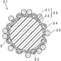
- FIG. 2 is a cross-sectional view showing conductive particles according to another embodiment of the present invention.
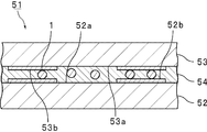
- FIG. 3 is a front sectional view schematically showing a connection structure using conductive particles according to an embodiment of the present invention.
- FIG. 1 is a cross-sectional view showing conductive particles according to an embodiment of the present invention.
- the conductive layer 3 is provided on the surface of the base particle 2.
- the conductive layer 3 has a nickel layer 11 provided on the surface of the base particle 2 and a metal layer 12 provided on the surface of the nickel layer 11.
- the conductive particles 1 may further include an insulating material disposed on the surface of the conductive layer 3.
- the metal layer 12 may not be provided.
- the metal layer 12 is preferably provided from the viewpoint of low resistance and the viewpoint of further suppressing the decrease in conductivity under severe conditions. That is, the conductive particles according to the present invention preferably have a metal layer provided on the surface of the nickel layer.
- the metal layer is a layer different from the nickel layer.
- a palladium layer may be formed, or a metal layer other than the palladium layer may be formed.
- the insulating substance is preferably an insulating resin layer or insulating particles.
- FIG. 2 is a cross-sectional view showing conductive particles according to another embodiment of the present invention.
- the conductive particle 21 includes a base particle 2 and a conductive layer 22.
- the conductive layer 22 is provided on the surface of the base particle 2.
- the conductive layer 22 has a nickel layer 31 provided on the surface of the base particle 2 and a metal layer 32 provided on the surface of the nickel layer 31.
- the conductive particle 21 includes a plurality of core substances 23 on the surface of the base particle 2.
- the nickel layer 31 and the conductive layer 22 cover the core material 23. By covering the core material 23 with the conductive layer 22, the conductive particles 21 have a plurality of protrusions 24 on the surface.
- the conductive particles 21 include a plurality of insulating substances 25 disposed on the surface of the conductive layer 22, that is, on the surface of the metal layer 32.
- the insulating substance 25 is an insulating particle.
- the insulating particles are preferably insulating resin particles. Instead of the insulating particles, an insulating resin layer may be arranged on the surface of the conductive layer 22.
- the conductive particles may include an insulating material disposed on the surface of the conductive layer.
- the conductive particles may include an insulating material attached on the surface of the conductive layer.
- the surface of the conductive layer may be covered with an insulating resin layer.
- the main feature of the conductive particles according to the present invention is that the alkali metal content A in the entire nickel layer exceeds 0 ⁇ g / g, and the alkali metal content B in the region of the nickel layer outer surface thickness of 30 nm is 80 ⁇ g / g or less.
- the content B is 0 ⁇ g / g or more, and may be 0 ⁇ g / g.
- the conductive structure is used when the connection structure using the conductive particles for connection between the electrodes is exposed to severe conditions. Elution ions derived from particles can be suppressed.
- connection structure when the connection structure is exposed to high temperature and high humidity, the eluted ions derived from the conductive particles can be suppressed.
- the conductive particles and the binder resin are mixed and coexisted.
- the binder resin it is difficult for the binder resin to be hardened due to the conductive particles.
- the content B is preferably 60 ⁇ g / g or less, more preferably 50 ⁇ g / g or less.
- the content B indicates the content of an alkali metal contained in a region having a thickness of 30 nm on the outer surface of the nickel layer with respect to the weight of the entire region having a thickness of 30 nm on the outer surface of the nickel layer.
- the region having a thickness of 30 nm on the outer surface of the nickel layer is, in other words, a region extending from the outer surface of the nickel layer to a distance of 30 nm inward in the thickness direction.
- the alkali metal content A in the entire nickel layer is preferably more than 0 ⁇ g / g and 50 ⁇ g / g or less.
- the alkali metal examples include lithium, sodium, potassium, rubidium and cesium.
- sodium ions and potassium ions are likely to be mixed and cause problems. Since the effect of the present invention can be obtained more remarkably, the alkali metal preferably contains sodium or potassium, and more preferably contains sodium.
- the nickel layer is preferably a nickel layer formed by an electroless plating reaction using an electroless plating solution containing a nickel salt and an alkali metal-containing reducing agent.
- the nickel layer is formed by an electroless plating reaction using an electroless plating solution containing a nickel salt and sodium hypophosphite (reducing agent). A layer is preferred.
- Examples of the substrate particles include resin particles, inorganic particles, organic-inorganic hybrid particles, and metal particles.
- the base material particles are preferably resin particles formed of a resin.
- the conductive particles are generally compressed after the conductive particles are arranged between the electrodes.
- the substrate particles are resin particles, the conductive particles are easily deformed by compression, and the contact area between the conductive particles and the electrode is increased. For this reason, the conduction
- the resin for forming the resin particles include polyolefins such as polyethylene, polypropylene, polystyrene, polyvinyl chloride, polyvinylidene chloride, polypropylene, polyisobutylene, and polybutadiene; acrylic resins such as polymethyl methacrylate and polymethyl acrylate; Polymerize one or more of alkylene terephthalate, polysulfone, polycarbonate, polyamide, phenol formaldehyde resin, melamine formaldehyde resin, benzoguanamine formaldehyde resin, urea formaldehyde resin, and various polymerizable monomers having ethylenically unsaturated groups. The polymer obtained by the above is used. By polymerizing one or more of various polymerizable monomers having an ethylenically unsaturated group, it is possible to design and synthesize resin particles having any compression property suitable for a
- the monomer having an ethylenically unsaturated group includes a non-crosslinkable monomer and a crosslinkable monomer. And so on.
- non-crosslinkable monomer examples include styrene monomers such as styrene and ⁇ -methylstyrene; carboxyl group-containing monomers such as (meth) acrylic acid, maleic acid, and maleic anhydride; (Meth) acrylate, ethyl (meth) acrylate, propyl (meth) acrylate, butyl (meth) acrylate, 2-ethylhexyl (meth) acrylate, lauryl (meth) acrylate, cetyl (meth) acrylate, stearyl (meth) acrylate, cyclohexyl ( Alkyl (meth) acrylates such as meth) acrylate and isobornyl (meth) acrylate; acids such as 2-hydroxyethyl (meth) acrylate, glycerol (meth) acrylate, polyoxyethylene (meth) acrylate and glycidyl (meth) acrylate Atom
- crosslinkable monomer examples include tetramethylolmethane tetra (meth) acrylate, tetramethylolmethane tri (meth) acrylate, tetramethylolmethane di (meth) acrylate, trimethylolpropane tri (meth) acrylate, and dipenta Erythritol hexa (meth) acrylate, dipentaerythritol penta (meth) acrylate, glycerol tri (meth) acrylate, glycerol di (meth) acrylate, (poly) ethylene glycol di (meth) acrylate, (poly) propylene glycol di (meth) Polyfunctional (meth) acrylates such as acrylate, (poly) tetramethylene di (meth) acrylate, 1,4-butanediol di (meth) acrylate; triallyl (iso) cyanurate, tri Lil
- the resin particles can be obtained by polymerizing the polymerizable monomer having an ethylenically unsaturated group by a known method. Examples of this method include a method of suspension polymerization in the presence of a radical polymerization initiator and a method of polymerizing a non-crosslinked seed particle by swelling a monomer together with a radical polymerization initiator.
- the substrate particles are inorganic particles or organic-inorganic hybrid particles
- examples of the inorganic material for forming the substrate particles include silica and carbon black. Although it does not specifically limit as the particle
- grains obtained by performing are mentioned.
- the substrate particles are metal particles
- examples of the metal for forming the metal particles include silver, copper, nickel, silicon, gold, and titanium.
- the substrate particles are preferably not metal particles.
- the average particle diameter of the substrate particles is preferably 1 ⁇ m or more, more preferably 2 ⁇ m or more, preferably 100 ⁇ m or less, more preferably 50 ⁇ m or less, still more preferably 30 ⁇ m or less, and particularly preferably 5 ⁇ m or less.
- the average particle diameter of the substrate particles is equal to or more than the above lower limit, the conduction reliability between the electrodes is further enhanced.
- interval between electrodes can be narrowed as the average particle diameter of a base particle is below the said upper limit.
- the above average particle diameter indicates the number average particle diameter.
- the average particle size can be measured using, for example, a Coulter counter (manufactured by Beckman Coulter).
- the average thickness of the nickel layer is 30 nm or more, preferably more than 30 ⁇ m, more preferably 45 nm or more, still more preferably 60 nm or more, preferably 1000 nm or less, more preferably 800 nm or less.
- the conductivity of the conductive particles is further increased.
- the average thickness of the nickel layer is not more than the above upper limit, the stress at the interface due to the difference in thermal expansion coefficient between the base particle and the nickel layer is relaxed, and the nickel layer becomes difficult to peel from the base particle.
- a method for forming a nickel layer on the surface of the substrate particles a method for forming a nickel layer by electroless plating is suitable.
- the average thickness of the metal layer is preferably 5 nm or more, more preferably 10 nm or more, preferably 500 nm or less, more preferably 400 nm. It is as follows. When the average thickness of the metal layer is not less than the above lower limit, the conductivity of the conductive particles is further increased. Furthermore, when the average thickness of the metal layer is not less than the above lower limit, the surface of the nickel layer can be relatively uniformly covered with the metal layer. For this reason, electroconductive particle becomes high tolerance with respect to an external environment, and a nickel layer becomes difficult to deteriorate. Therefore, the conductivity of the entire conductive layer in the conductive particles can be further increased. When the average thickness of the metal layer is not more than the above upper limit, the cost of the conductive particles is reduced.
- an electroless plating solution containing a metal-containing compound such as a palladium salt and a reducing agent is used, and the metal layer is electrolessly plated.
- a method of forming a metal layer by electroplating As a method for forming the metal layer (the palladium layer or the like) on the surface of the nickel layer, an electroless plating solution containing a metal-containing compound such as a palladium salt and a reducing agent is used, and the metal layer is electrolessly plated. And a method of forming a metal layer by electroplating.
- examples of the metal for constituting the metal layer include gold, silver, copper, platinum, zinc, iron, lead, tin, aluminum, Examples include cobalt, indium, chromium, titanium, antimony, germanium, cadmium, bismuth, thallium, tin-lead alloy, tin-copper alloy, tin-silver alloy, and tin-lead-silver alloy.
- tin-doped indium oxide (ITO) may be used as the metal.
- ITO tin-doped indium oxide
- the said metal only 1 type may be used, 2 or more types may be used together, and an alloy may be sufficient as it.
- the conductive particles according to the present invention preferably have protrusions on the surface.
- the conductive particles preferably have protrusions on the outer surface of the conductive layer, preferably have protrusions on the outer surface of the nickel layer, preferably have protrusions on the outer surface of the metal layer, and the outer surface of the palladium layer. It is preferable to have a protrusion on the surface. It is preferable that there are a plurality of protrusions.
- An oxide film is often formed on the surface of the electrode connected by the conductive particles. When conductive particles having protrusions are used, the oxide film is effectively eliminated by the protrusions by placing the conductive particles between the electrodes and pressing them.
- an electrode and the conductive layer of electroconductive particle can be contacted still more reliably, and the connection resistance between electrodes can be made low.
- the conductive particles have an insulating material on the surface, or when the conductive particles are dispersed in a binder resin and used as an anisotropic conductive material, the conductive particles and the conductive particles The resin between the electrodes can be effectively eliminated. For this reason, the conduction
- a method of forming protrusions on the surface of the conductive particles a method of forming a conductive layer by electroless plating after attaching a core substance to the surface of the base particles, and electroless plating on the surface of the base particles
- Examples include a method of forming a conductive layer by, attaching a core substance, and further forming a conductive layer by electroless plating.
- a method for attaching the core substance to the surface of the base particle for example, a conductive substance that becomes the core substance is added to the dispersion of the base particle, and the core substance is added to the surface of the base particle, for example, A method of accumulating and adhering by van der Waals force, and adding a conductive substance as a core substance to the container containing the base particle, and then the core on the surface of the base particle by mechanical action such as rotation of the container Examples include a method of attaching a substance. Especially, since the quantity of the core substance to adhere is easy to control, the method of making a core substance accumulate and adhere on the surface of the base particle in a dispersion liquid is preferable.
- Examples of the conductive substance constituting the core substance include metals, metal oxides, conductive nonmetals such as graphite, and conductive polymers.
- Examples of the conductive polymer include polyacetylene. Among them, metal is preferable because conductivity can be increased.
- Examples of the metal include gold, silver, copper, platinum, zinc, iron, lead, tin, aluminum, cobalt, indium, nickel, chromium, titanium, antimony, bismuth, germanium and cadmium, and tin-lead.
- Examples thereof include alloys composed of two or more metals such as alloys, tin-copper alloys, tin-silver alloys, and tin-lead-silver alloys. Of these, nickel, copper, silver or gold is preferable.
- the metal constituting the core material may be the same as or different from the metal constituting the conductive layer.
- Examples of the metal oxide include alumina, silica and zirconia.
- the core substance is applied to the surface of the nickel plating metal layer after the nickel plating process or to the surface of the metal plating layer such as palladium on the nickel layer by physical or mechanical impact. You may use the method of making it adhere. In this case, a physical or mechanical hybridization method may be used. In the physical or mechanical hybridization method, a hybridizer or the like is used.
- the conductive particles according to the present invention preferably include an insulating material disposed on the surface of the conductive layer (the metal layer such as the nickel layer or the palladium layer).
- the metal layer such as the nickel layer or the palladium layer.
- the conductive particles when used for connection between the electrodes, a short circuit between adjacent electrodes can be prevented.
- an insulating material is present between the plurality of electrodes, so that it is possible to prevent a short circuit between electrodes adjacent in the lateral direction instead of between the upper and lower electrodes.
- the insulating substance between the conductive layer of an electroconductive particle and an electrode can be easily excluded by pressurizing electroconductive particle with two electrodes in the case of the connection between electrodes.
- the insulating substance is preferably an insulating resin layer or insulating particles.
- the insulating particles are preferably insulating resin particles.
- the insulating material include polyolefins, (meth) acrylate polymers, (meth) acrylate copolymers, block polymers, thermoplastic resins, crosslinked thermoplastic resins, thermosetting resins, and water-soluble resins. Etc.
- thermoplastic resin examples include vinyl polymers and vinyl copolymers.
- thermosetting resin an epoxy resin, a phenol resin, a melamine resin, etc.
- water-soluble resin examples include polyvinyl alcohol, polyacrylic acid, polyacrylamide, polyvinyl pyrrolidone, polyethylene oxide, and methyl cellulose.
- the conductive particles according to the present invention include insulating particles attached to the surface of the conductive layer.
- the conductive particles when used for the connection between the electrodes, not only can the short circuit between the laterally adjacent electrodes be further prevented, but also the connection resistance between the connected upper and lower electrodes can be further reduced. Can do.
- Examples of methods for attaching insulating particles to the surface of the conductive layer include chemical methods and physical or mechanical methods.
- the chemical method for example, as disclosed in WO2003 / 25955A1, insulating particles are attached on the conductive layer of the metal surface particles by a heteroaggregation method using van der Waals force or electrostatic force, and further required.
- a chemical bonding method may be mentioned.
- the physical or mechanical method include spray drying, hybridization, electrostatic adhesion, spraying, dipping, and vacuum deposition.
- a method of attaching an insulating substance to the surface of the conductive layer through a chemical bond is preferable because the insulating substance is difficult to be detached.
- the particle diameter of the insulating particles is preferably 1/5 or less of the particle diameter of the conductive particles. In this case, the particle diameter of the insulating particles does not become too large, and the electrical connection by the conductive layer is more reliably achieved. When the particle diameter of the insulating particles is 1/5 or less of the particle diameter of the conductive particles, the insulating particles are efficiently adsorbed on the surface of the conductive layer when the insulating particles are adhered by the hetero-aggregation method. Can do.
- the particle diameter of the insulating particles is preferably 5 nm or more, more preferably 10 nm or more, preferably 1000 nm or less, more preferably 500 nm or less.
- the particle diameter of the insulating particles When the particle diameter of the insulating particles is equal to or larger than the lower limit, the distance between adjacent conductive particles becomes larger than the electron hopping distance, and leakage hardly occurs. When the particle diameter of the insulating particles is not more than the above upper limit, the pressure and the amount of heat required for thermocompression bonding are reduced.
- the particle size CV value of the insulating particles is preferably 20% or less.
- the CV value of the particle diameter is calculated by the following formula.
- Particle size CV value (%) standard deviation of particle size / average particle size ⁇ 100
- the particle size distribution can be measured with a particle size distribution meter before coating the metal surface particles, and can be measured with image analysis of SEM photographs after coating.
- the insulating material coverage is preferably 5% or more, and preferably 70% or less.
- the coverage with the insulating material is the area of the portion covered with the insulating material in the entire surface area of the metal surface particles.
- the coverage is 5% or more, adjacent conductive particles are more reliably insulated by an insulating substance.
- the coverage is 70% or less, it is not necessary to apply heat and pressure more than necessary when connecting the electrodes, and the performance of the binder resin can be suppressed from being reduced by the excluded insulating substance.
- the insulating particles are not particularly limited, but known inorganic particles and organic polymer particles are applicable.
- the inorganic particles include insulating inorganic particles such as alumina, silica, and zirconia.
- the organic polymer particles are preferably resin particles obtained by (co) polymerizing one or more monomers having an unsaturated double bond.
- the monomer having an unsaturated double bond include (meth) acrylic acid; methyl (meth) acrylate, ethyl (meth) acrylate, propyl (meth) acrylate, butyl (meth) acrylate, and 2-ethylhexyl (meth).
- the insulating particles have a polar functional group in order to adhere to the conductive layer of the conductive particles by heteroaggregation.
- the polar functional group include an ammonium group, a sulfonium group, a phosphate group, and a hydroxysilyl group.
- the polar functional group can be introduced by copolymerizing a monomer having the polar functional group and an unsaturated double bond.
- Examples of the monomer having an ammonium group include N, N-dimethylaminoethyl methacrylate, N, N-dimethylaminopropyl acrylamide, and N, N, N-trimethyl-N-2-methacryloyloxyethylammonium chloride. It is done.
- Examples of the monomer having a sulfonium group include phenyldimethylsulfonium methylsulfate methacrylate.
- Examples of the monomer having a phosphoric acid group include acid phosphooxyethyl methacrylate, acid phosphooxypropyl methacrylate, acid phosphooxypolyoxyethylene glycol monomethacrylate, and acid phosphooxypolyoxypropylene glycol monomethacrylate.
- Examples of the monomer having a hydroxysilyl group include vinyltrihydroxysilane and 3-methacryloxypropyltrihydroxysilane.
- a method using a radical initiator having a polar group as an initiator when the monomer having an unsaturated double bond is polymerized may be mentioned. It is done.
- the radical initiator include 2,2′-azobis ⁇ 2-methyl-N- [2- (1-hydroxy-butyl)]-propionamide ⁇ , 2,2′-azobis [2- (2- Imidazolin-2-yl) propane], 2,2′-azobis (2-amidinopropane) and salts thereof.
- the method for producing conductive particles according to the present invention includes a step of forming a nickel layer on the surface of a base particle by an electroless plating reaction using an electroless plating solution containing a nickel salt and an alkali metal-containing reducing agent. (Electroless plating step).
- the alkali metal ion concentration (mol / L) in the electroless plating solution at the end of the electroless plating reaction is the same as that in the electroless plating solution at the end of the electroless plating reaction.
- the nickel ion concentration (mol / L) is 4 times or less, the electroless plating reaction is terminated.
- conductive particles in which the content of the alkali metal in the entire nickel layer exceeds 0 ⁇ g / g and the content B of the alkali metal in the region of 30 nm thickness on the outer surface of the nickel layer is 80 ⁇ g / g or less are obtained. .
- the content A of the alkali metal exceeds 0 ⁇ g / g.
- the alkali metal ion concentration includes alkali metal ions in the electroless plating solution.
- the nickel ion concentration includes nickel ions in the electroless plating solution.
- conductive particles in which the content A of the alkali metal in the entire nickel layer exceeds 0 ⁇ g / g and is 50 ⁇ g / g or less are obtained.
- the nickel ion concentration in the electroless plating solution decreases as the thickness of the nickel layer increases. It was noted that the alkali metal ion concentration in the electroless plating solution was increased. As a result, in the nickel layer, the alkali metal ion concentration tends to increase from the inner surface to the outer surface, and the alkali metal content in the vicinity of the outer surface of the nickel layer is particularly high.
- the electroless plating reaction is terminated before the alkali metal ion concentration (mol / L) in the electroless plating solution at the end of the electroless plating reaction becomes too high. .
- the inventors have determined that the alkali metal ion concentration (mol / L) in the electroless plating solution at the end of the electroless plating reaction is the nickel ion concentration in the electroless plating solution at the end of the electroless plating reaction. It has been found that the content of alkali metal in the vicinity of the outer surface of nickel can be controlled so as not to increase by terminating the electroless plating reaction when it is 4 times or less (mol / L). As a result, the alkali metal content B in the 30 nm thick region of the outer surface of the nickel layer is reduced. As a result of the content B being reduced, the content A of the alkali metal in the entire nickel layer is also reduced.
- the electroless plating reaction when performing an electroless plating reaction, the electroless plating reaction is allowed to proceed until the nickel in the plating solution is sufficiently consumed. This is to make effective use of nickel. However, when the electroless plating reaction proceeds to the general nickel consumption in this way, the amount of alkali metal contained in the nickel layer increases. In the method for producing conductive particles according to the present invention, even if nickel is not sufficiently consumed, the plating reaction is actively terminated, and the content B of alkali metal near the outer surface of nickel is reduced. Preferably, the alkali metal content A in the entire nickel layer is also reduced.
- an etching process and a catalytic process are performed prior to the electroless plating process.
- an example of a method for forming a nickel layer on the surface of the resin particles by electroless plating will be described in more detail.
- an oxidizing agent such as chromic acid, a sulfuric acid-chromic acid mixed solution or a permanganic acid solution, a strong acid such as hydrochloric acid or sulfuric acid, a strong alkaline solution such as sodium hydroxide or potassium hydroxide, and various other commercially available etching agents.
- Etc. are used to form minute irregularities on the surface of the resin particles. This enhances the adhesion of the nickel layer.
- a liquid agent containing a halogen ion it is preferable to perform sufficient washing so that no halogen remains.
- a catalyst layer serving as a starting point for forming a plating layer by electroless plating is formed on the surface of the resin particles.
- the surface of the resin particle is activated with an acid solution or an alkali solution
- a method of depositing palladium for example, a method of depositing palladium.
- the reducing agent sodium hypophosphite, potassium hypophosphite, dimethylamine borane or the like is used.
- a nickel plating bath electroless plating solution containing a nickel salt and an alkali metal-containing reducing agent
- nickel By immersing the resin particles in the nickel plating bath, nickel can be deposited on the surface of the resin particles on which the catalyst is formed.
- a phosphorus-based reducing agent is preferably used as the alkali metal-containing reducing agent.
- sodium hypophosphite or potassium hypophosphite is preferably used.
- the alkali metal-containing reducing agent is preferably a sodium-containing reducing agent or a potassium-containing reducing agent, and is preferably a sodium-containing reducing agent.
- the method for producing conductive particles according to the present invention preferably further includes a step of forming a metal layer (electroless plating step) using an electroless plating solution containing a metal on the surface of the nickel layer. More preferably, the method for producing conductive particles according to the present invention further includes a step of forming a palladium layer on the surface of the nickel layer using an electroless plating solution containing palladium.
- the anisotropic conductive material according to the present invention includes the above-described conductive particles and a binder resin.
- the binder resin is not particularly limited.
- As the binder resin a known insulating resin is used.
- a polymerization catalyst or a curing catalyst is blended.
- a polymerization initiator or a curing agent is blended with the binder resin.
- the binder resin is preferably a curable resin.
- the anisotropic conductive material preferably contains a polymerization initiator or a curing agent.
- the curable resin is preferably an epoxy resin.
- the anisotropic conductive material preferably includes a curing agent, and more preferably includes an anionic curing agent.
- an anisotropic conductive film often uses a curing system including an epoxy resin and an anionic curing agent.
- Conventional conductive particles that do not control the alkali metal content B in the vicinity of the outer surface tend to cause problems such as curing delay and poor curing in such a curing system.
- the detailed mechanism is unknown, it is considered that the anion component generated in the curing process of these curing systems interacts with alkali metal ions derived from the conductive particles to inhibit the curing reaction. .
- Even in a curing system other than an anionic system unexpected curing failure or curing abnormality such as gelation may occur.
- the alkali metal ions are eluted from the pinholes and crevices of the metal, or the portions where the underlying nickel layer is exposed due to non-uniform plating, and the above-described hardening inhibition occurs.
- the anisotropic conductive material includes, for example, a filler, an extender, a softener, a plasticizer, a polymerization catalyst, a curing catalyst, a colorant, an antioxidant, and a heat stabilizer. Further, various additives such as a light stabilizer, an ultraviolet absorber, a lubricant, an antistatic agent and a flame retardant may be contained.
- the method for dispersing the conductive particles in the binder resin is not particularly limited, and a conventionally known dispersion method can be used.
- Examples of a method for dispersing the conductive particles in the binder resin include a method in which the conductive particles are added to the binder resin and then kneaded and dispersed with a planetary mixer or the like. The conductive particles are dispersed in water. Alternatively, after uniformly dispersing in an organic solvent using a homogenizer or the like, it is added to the binder resin and kneaded with a planetary mixer or the like, and the binder resin is diluted with water or an organic solvent. Then, the method of adding the said electroconductive particle, kneading with a planetary mixer etc. and disperse
- distributing is mentioned.
- the anisotropic conductive material according to the present invention can be used as an anisotropic conductive paste and an anisotropic conductive film.
- the anisotropic conductive material according to the present invention is an anisotropic conductive film
- a film-like adhesive not containing conductive particles is laminated on the anisotropic conductive film containing conductive particles. Also good.
- the anisotropic conductive paste and the anisotropic conductive film include anisotropic conductive ink, anisotropic conductive adhesive and anisotropic conductive sheet.
- the content of the binder resin is preferably 10% by weight or more, more preferably 30% by weight or more, still more preferably 50% by weight or more, particularly preferably 70% by weight or more, preferably It is 99.99 weight% or less, More preferably, it is 99.9 weight% or less.
- the content of the binder resin is not less than the above lower limit and not more than the above upper limit, the conductive particles can be efficiently disposed between the electrodes, and the conduction reliability between the electrodes can be further enhanced.
- the content of the conductive particles is preferably 0.01% by weight or more, more preferably 0.1% by weight or more, preferably 20% by weight or less, more preferably 10% by weight. % Or less.
- the content of the conductive particles is not less than the above lower limit and not more than the above upper limit, the conduction reliability between the electrodes is further enhanced.
- connection structure can be obtained by connecting the connection target members using the conductive particles according to the present invention or using an anisotropic conductive material containing the conductive particles and a binder resin.
- connection structure includes a first connection target member, a second connection target member, and a connection part connecting the first and second connection target members, the connection part of the present invention.
- a connection structure formed of conductive particles or an anisotropic conductive material containing the conductive particles and a binder resin is preferable.
- the connection portion itself is conductive particles. That is, the first and second connection target members are connected by the conductive particles.
- FIG. 3 is a front sectional view schematically showing a connection structure using conductive particles according to an embodiment of the present invention.
- a connection structure 51 shown in FIG. 3 includes a first connection target member 52, a second connection target member 53, and a connection portion 54 connecting the first and second connection target members 52 and 53.
- the connection portion 54 is formed by curing an anisotropic conductive material including the conductive particles 1.
- the conductive particles 1 are schematically shown for convenience of illustration. Instead of the conductive particles 1, conductive particles 21 may be used.
- a plurality of electrodes 52 b are provided on the upper surface 52 a (front surface) of the first connection target member 52.
- a plurality of electrodes 53 b are provided on the lower surface 53 a (front surface) of the second connection target member 53.
- the electrode 52 b and the electrode 53 b are electrically connected by one or a plurality of conductive particles 1. Therefore, the first and second connection target members 52 and 53 are electrically connected by the conductive particles 1.
- the manufacturing method of the connection structure is not particularly limited.
- the anisotropic conductive material is disposed between the first connection target member and the second connection target member to obtain a laminate, and then the laminate is heated. And a method of applying pressure.
- the pressurizing pressure is about 9.8 ⁇ 10 4 to 4.9 ⁇ 10 6 Pa.
- the heating temperature is about 120 to 220 ° C.
- connection target member examples include electronic components such as semiconductor chips, capacitors, and diodes, and circuit boards such as printed boards, flexible printed boards, and glass boards.
- the electrode provided on the connection target member examples include metal electrodes such as a gold electrode, a nickel electrode, a tin electrode, an aluminum electrode, a copper electrode, a molybdenum electrode, and a tungsten electrode.
- the electrode is preferably a gold electrode, a nickel electrode, a tin electrode, or a copper electrode.
- the connection target member is a glass substrate, the electrode is preferably an aluminum electrode, a copper electrode, a molybdenum electrode, or a tungsten electrode.
- the electrode formed only with aluminum may be sufficient and the electrode by which the aluminum layer was laminated
- the material for the metal oxide layer include indium oxide doped with a trivalent metal element and zinc oxide doped with a trivalent metal element. Examples of the trivalent metal element include Sn, Al, and Ga.
- Example 1 Electroless nickel plating step Divinylbenzene resin particles having an average particle diameter of 4 ⁇ m were treated with a 10 wt% solution of an ion adsorbent for 5 minutes, and then treated with a 0.01 wt% palladium sulfate aqueous solution for 5 minutes. Thereafter, dimethylamine borane was added for reduction treatment, filtration, and washing to obtain resin particles to which palladium was attached.
- An electroless plating solution containing 34% by weight of nickel sulfate hexahydrate, 24% by weight of sodium hypophosphite monohydrate, 15% by weight of ammonia and 5% by weight of succinic acid (the concentration of sodium mol in the electroless plating solution is The nickel mol concentration was 2 times or less).
- the electroless plating solution was continuously dropped into the slurry and stirred to advance the plating reaction.
- the plating reaction was completed when the sodium ion concentration in the electroless plating solution was 2.5 times the nickel ion concentration. In this way, a nickel layer was formed on the surface of the resin particles to obtain nickel plated particles.
- the nickel layer had a thickness of 0.1 ⁇ m.
- Electroless palladium plating step 10 g of the obtained nickel-plated particles were dispersed in 500 mL of ion-exchanged water using an ultrasonic treatment machine to obtain a particle suspension. While stirring the suspension at 50 ° C., 0.02 mol / L of palladium sulfate, 0.04 mol / L of ethylenediamine as a complexing agent, 0.06 mol / L of sodium formate as a reducing agent, and pH 10.0 containing a crystal modifier. The electroless plating solution was gradually added to perform electroless palladium plating. When the thickness of the palladium layer reached 0.03 ⁇ m, the electroless palladium plating was finished. Next, by washing and vacuum drying, conductive particles having a palladium layer formed on the surface of the nickel layer were obtained.
- Example 2 In the electroless nickel plating step, when the sodium ion concentration in the electroless plating solution at the end of the electroless plating reaction is 3.3 times the nickel ion concentration, Example 1 except that the plating reaction is ended. Similarly, nickel plating particles were obtained.
- Example 3 In the electroless nickel plating step, Example 1 except that the plating reaction was terminated when the sodium ion concentration in the electroless plating solution at the end of the electroless plating reaction was 4.0 times the nickel ion concentration. Similarly, nickel plating particles were obtained.
- Example 4 Electroless nickel plating step (step of forming protrusions on the surface of the nickel layer) 1-1) Palladium adhesion step 10 g of divinylbenzene resin particles having an average particle diameter of 4 ⁇ m were prepared. The resin particles were etched and washed with water. Next, resin particles were added to 100 mL of a palladium-catalyzed solution containing 8% by weight of a palladium catalyst and stirred. Thereafter, resin particles were added to a 0.5 wt% dimethylamine borane solution having a pH of 6, filtered, and washed to obtain resin particles having palladium attached thereto.
- Electroless palladium plating step Conductive particles having a palladium layer formed on the surface of the nickel layer are obtained by performing the same electroless palladium plating step as in Example 1 using 10 g of the obtained nickel plating particles. Obtained. The obtained conductive particles had protrusions on the surface.
- the conductive particles were obtained in the same manner as in Example 4 except that the change was made to). The obtained conductive particles had protrusions on the surface.
- Example 6 Preparation of insulating resin particles A 1000 mL separable flask equipped with a four-necked separable cover, a stirring blade, a three-way cock, a condenser tube and a temperature probe was charged with 100 mmol of methyl methacrylate and N, N, N- Ion exchange of a monomer composition containing 1 mmol of trimethyl-N-2-methacryloyloxyethylammonium chloride and 1 mmol of 2,2′-azobis (2-amidinopropane) dihydrochloride so that the solid content is 5% by weight After weighing in water, the mixture was stirred at 200 rpm and polymerized at 70 ° C. for 24 hours in a nitrogen atmosphere. After completion of the reaction, freeze drying was performed to obtain insulating resin particles having an ammonium group on the surface, an average particle diameter of 220 nm, and a CV value of 10%.
- the insulating resin particles were dispersed in ion exchange water under ultrasonic vibration to obtain a 10 wt% aqueous dispersion of insulating resin particles.
- Example 5 10 g of conductive particles having protrusions on the surface obtained in Example 5 were dispersed in 500 mL of ion-exchanged water, 4 g of an aqueous dispersion of insulating resin particles was added, and the mixture was stirred at room temperature for 6 hours. After filtration with a 3 ⁇ m mesh filter, the particles were further washed with methanol and dried to obtain conductive particles having insulating resin particles attached thereto.
- the conductive particles were obtained in the same manner as in Example 1 except that the above was changed.
- Example 8 Except having changed the electroconductive particle obtained in Example 5 into the electroconductive particle obtained in Example 1, it carried out similarly to Example 6, and obtained the electroconductive particle to which the insulating resin particle adhered.
- Example 9 Conductive particles with insulating resin particles adhered in the same manner as in Example 6 except that the conductive particles obtained in Example 5 were changed to conductive particles having protrusions on the surface obtained in Example 4. Got.
- Example 10 Except having changed the electroconductive particle obtained in Example 5 into the electroconductive particle obtained in Example 7, it carried out similarly to Example 6, and obtained the electroconductive particle to which the insulating resin particle adhered.
- Example 11 In the electroless palladium plating step, the same as in Example 1 except that the complexing agent was changed to an electroless plating solution having a pH of 9.0 containing 35 mmol / L of ethylenediamine, 50 mmol / L of sodium formate as a reducing agent, and a crystal modifier. Thus, conductive particles having a palladium layer formed on the surface of the nickel layer were obtained.
- Example 12 In the same manner as in Example 1, except that sodium hypophosphite monohydrate in the electroless nickel plating step of Example 1 was changed to potassium hypophosphite monohydrate, palladium was deposited on the surface of the nickel layer. The electroconductive particle in which the layer was formed was obtained.
- Example 13 Conductive particles (nickel plated particles) in which a nickel layer is formed on the surface of the resin particles in the same manner as in Example 1, except that the electroless palladium plating step following the electroless nickel plating step of Example 1 was not performed. Got.
- Example 14 A nickel layer is formed on the surface of the resin particles in the same manner as in Example 4 except that the electroless palladium plating step following the electroless nickel plating step of Example 4 is not performed. Particles (nickel plating particles) were obtained.
- Example 1 In the electroless nickel plating step, when the sodium ion concentration in the electroless plating solution at the end of the electroless plating reaction is 4.2 times the nickel ion concentration, Example 1 is the same as in Example 1 except that the plating reaction is ended. Similarly, nickel plating particles were obtained.
- the obtained particles were washed with distilled water and methanol and then classified to obtain resin particles having an average particle size of 4.1 ⁇ m and a coefficient of variation of 5.0%.
- Etching was performed by dispersing 10 g of the obtained resin particles in a pre-dip solution for powder plating (Okuno Pharmaceutical Co., Ltd.) and stirring at 30 ° C. for 30 minutes. After washing with water, the solution was added to 100 ml of a Pd catalyst containing 1% by weight of palladium sulfate and stirred at 30 ° C. for 30 minutes to adsorb palladium ions to the particles. The particles were collected by filtration and washed with water, and then added to a 0.5% by weight dimethylamine borane solution (adjusted to pH 6.0) to obtain resin particles with activated Pd.
- a particle suspension was obtained by adding 500 ml of distilled water to the obtained Pd activated resin particles and sufficiently dispersing using an ultrasonic processor. While stirring this suspension at 50 ° C., an electroless plating solution (pH: 7.5) consisting of nickel sulfate (hexahydrate) 50 g / L, sodium hypophosphite 40 g / L, and citric acid 50 g / L. was added gradually and electroless nickel plating was performed. When the metal coating layer became approximately 0.10 ⁇ m, the addition of the electroless plating solution was stopped, and after substitution with alcohol, the particles were vacuum dried to obtain conductive particles.
- an electroless plating solution pH: 7.5
- the addition of the electroless plating solution was stopped, and after substitution with alcohol, the particles were vacuum dried to obtain conductive particles.
- Comparative Example 4 After etching 10 g of the resin particles obtained in Comparative Example 3 in the same manner as in Comparative Example 3, a catalyst comprising 10 mL of a Pd catalyst containing tin chloride (Okuno Pharmaceutical Co., Ltd., catalyst), 10 mL of 37% hydrochloric acid, and 10 mL of ethanol. It was added to the liquid and stirred at 30 ° C. for 30 minutes. The particles were collected by filtration, washed with 100 mL of 5% sulfuric acid, and then washed with water to obtain resin particles in which Pd was activated. The particles were electroless nickel-plated in the same manner as in Comparative Example 3, substituted with alcohol, and then vacuum dried to obtain conductive particles.
- a catalyst comprising 10 mL of a Pd catalyst containing tin chloride (Okuno Pharmaceutical Co., Ltd., catalyst), 10 mL of 37% hydrochloric acid, and 10 mL of ethanol. It was added to the liquid and stirred at 30
- Comparative Example 5 The conductive particles obtained in Comparative Example 4 were dispersed again in 1000 mL of distilled water (specific resistance 18 M ⁇ ), and were stirred and washed at 121 ° C. for 10 hours under a pressure of 0.1 MPa in the same manner as in Comparative Example 3 to obtain conductive particles. Obtained.
- Comparative Example 6 The conductive particles obtained in Comparative Example 5 were stirred and washed at 121 ° C. for 10 hours under a pressure of 0.1 MPa to obtain conductive particles.
- spacers for liquid crystal display elements are spread on the alignment film side of one glass substrate so as to be 100 to 200 pieces per 1 mm 2 using a dry spreader (DISPA- ⁇ R, manufactured by Nissin Engineering Co., Ltd.). did. Further, after forming a peripheral sealant around the other glass substrate so as to expose the drive electrode, the glass substrate on which spacers are dispersed is arranged so as to face the rubbing direction at 90 °, and the two glass substrates Were pasted together. Then, it processed at 160 degreeC for 90 minute (s), the sealing agent was hardened, and the empty cell (screen which does not contain a liquid crystal) was produced. An STN type liquid crystal containing a chiral agent (“RDP-95873” manufactured by DIC) was injected into the resulting empty cell, and then the injection port was closed with a sealant to produce an STN type liquid crystal display device. For 30 minutes.
- the drive IC used was a STN-LCD common driver (LC41385KBR) manufactured by Sanyo Semiconductor.
- An anisotropic conductive material was prepared for mounting the driving IC. That is, an anisotropic conductive paste containing 10 parts by weight of each conductive particle obtained in Examples and Comparative Examples and 90 parts by weight of XAP-0289 (manufactured by Kyocera Chemical Co.) containing a binder resin was prepared.
- connection structure was left for 100 hours in a non-energized state at 40 ° C. and a humidity of 90%. A lighting test of the connection structure (liquid crystal display element) after being left was performed, and the failure rate of 4000 connection structures was evaluated.
- ⁇ Failure rate is less than 0.05% ⁇ : Failure rate is 0.05% or more, less than 0.25% ⁇ : Failure rate is 0.25% or more
Landscapes
- Physics & Mathematics (AREA)
- Chemical & Material Sciences (AREA)
- Dispersion Chemistry (AREA)
- Spectroscopy & Molecular Physics (AREA)
- Conductive Materials (AREA)
- Chemically Coating (AREA)
- Non-Insulated Conductors (AREA)
- Powder Metallurgy (AREA)
Abstract
Description
本発明に係る導電性粒子の製造方法は、基材粒子の表面上に、ニッケル塩とアルカリ金属含有還元剤とを含む無電解めっき液を用いて、無電解めっき反応によりニッケル層を形成する工程(無電解めっき工程)を備える。
本発明に係る異方性導電材料は、上述した導電性粒子と、バインダー樹脂とを含む。上記バインダー樹脂は特に限定されない。上記バインダー樹脂として、公知の絶縁性の樹脂が用いられる。
本発明に係る導電性粒子を用いて又は該導電性粒子とバインダー樹脂とを含む異方性導電材料を用いて、接続対象部材を接続することにより、接続構造体を得ることができる。
(1)無電解ニッケルめっき工程
平均粒子径4μmのジビニルベンゼン樹脂粒子を、イオン吸着剤の10重量%溶液により5分間処理し、次に硫酸パラジウム0.01重量%水溶液により5分間処理した。その後、ジメチルアミンボランを加えて還元処理し、ろ過し、洗浄することにより、パラジウムが付着された樹脂粒子を得た。
得られたニッケルめっき粒子10gを、超音波処理機により、イオン交換水500mLに分散させ、粒子懸濁液を得た。この懸濁液を50℃で攪拌しながら、硫酸パラジウム0.02mol/L、錯化剤としてエチレンジアミン0.04mol/L、還元剤として蟻酸ナトリウム0.06mol/L及び結晶調整剤を含むpH10.0の無電解めっき液を徐々に添加し、無電解パラジウムめっきを行った。パラジウム層の厚みが0.03μmになった時点で無電解パラジウムめっきを終了した。次に、洗浄し、真空乾燥することにより、ニッケル層の表面にパラジウム層が形成された導電性粒子を得た。
無電解ニッケルめっき工程において、無電解めっき反応終了時の上記無電解めっき液中のナトリウムイオン濃度がニッケルイオン濃度の3.3倍であるときに、めっき反応を終了したこと以外は実施例1と同様にして、ニッケルめっき粒子を得た。
無電解ニッケルめっき工程において、無電解めっき反応終了時の上記無電解めっき液中のナトリウムイオン濃度がニッケルイオン濃度の4.0倍であるときに、めっき反応を終了したこと以外は実施例1と同様にして、ニッケルめっき粒子を得た。
(1)無電解ニッケルめっき工程(ニッケル層の表面に突起を形成する工程)
1-1)パラジウム付着工程
平均粒子径4μmのジビニルベンゼン樹脂粒子10gを用意した。この樹脂粒子をエッチングし、水洗した。次に、パラジウム触媒を8重量%含むパラジウム触媒化液100mL中に樹脂粒子を添加し、攪拌した。その後、pH6の0.5重量%ジメチルアミンボラン液に樹脂粒子を添加し、ろ過し、洗浄して、パラジウムが付着された樹脂粒子を得た。
パラジウムが付着された樹脂粒子をイオン交換水300mL中で3分間攪拌し、分散させ、分散液を得た。次に、金属ニッケル粒子スラリー(三井金属社製「2020SUS」、平均粒子径200nm)1gを3分間かけて上記分散液に添加し、芯物質が付着された樹脂粒子を得た。
芯物質が付着された樹脂粒子にイオン交換水500mLを加え、樹脂粒子を十分に分散させて懸濁液を得た。この懸濁液を攪拌しながら、硫酸ニッケル6水和物50g/L、次亜リン酸ナトリウム1水和物30g/L及びクエン酸50g/Lを含むpH5.0の無電解ニッケルめっき液を徐々に添加し、無電解ニッケルめっきを行った。無電解めっき液中のナトリウムイオン濃度がニッケルイオン濃度の2.5倍であるときに、めっき反応を終了した。このようにして、樹脂粒子の表面にニッケル層を形成し、表面に突起を有するニッケルめっき粒子を得た。なお、ニッケル層の厚みは、0.1μmであった。
得られたニッケルめっき粒子10gを用いて、実施例1と同様の無電解パラジウムめっき工程を行うことにより、ニッケル層の表面にパラジウム層が形成された導電性粒子を得た。得られた導電性粒子は、表面に突起を有していた。
ジビニルベンゼン樹脂粒子を、1,4-ブタンジオールジアクリレートと、テトラメチロールメタンテトラアクリレートとの共重合樹脂粒子(1,4-ブタンジオールジアクリレート:テトラメチロールメタンテトラアクリレート=95重量%:5重量%)に変更したこと以外は、実施例4と同様にして導電性粒子を得た。得られた導電性粒子は、表面に突起を有していた。
(1)絶縁性樹脂粒子の作製
4ツ口セパラブルカバー、攪拌翼、三方コック、冷却管及び温度プローブが取り付けられた1000mLのセパラブルフラスコに、メタクリル酸メチル100mmolと、N,N,N-トリメチル-N-2-メタクリロイルオキシエチルアンモニウムクロライド1mmolと、2,2’-アゾビス(2-アミジノプロパン)二塩酸塩1mmolとを含むモノマー組成物を固形分率が5重量%となるようにイオン交換水に秤取した後、200rpmで攪拌し、窒素雰囲気下70℃で24時間重合を行った。反応終了後、凍結乾燥して、表面にアンモニウム基を有し、平均粒子径220nm及びCV値10%の絶縁性樹脂粒子を得た。
ジビニルベンゼン樹脂粒子を、1,4-ブタンジオールジアクリレートと、テトラメチロールメタンテトラアクリレートとの共重合樹脂粒子(1,4-ブタンジオールジアクリレート:テトラメチロールメタンテトラアクリレート=95重量%:5重量%)に変更したこと以外は、実施例1と同様にして導電性粒子を得た。
実施例5で得られた導電性粒子を実施例1で得られた導電性粒子に変更したこと以外は、実施例6と同様にして絶縁性樹脂粒子が付着した導電性粒子を得た。
実施例5で得られた導電性粒子を実施例4で得られた表面に突起を有する導電性粒子に変更したこと以外は、実施例6と同様にして絶縁性樹脂粒子が付着した導電性粒子を得た。
実施例5で得られた導電性粒子を実施例7で得られた導電性粒子に変更したこと以外は、実施例6と同様にして絶縁性樹脂粒子が付着した導電性粒子を得た。
無電解パラジウムめっき工程において、錯化剤としてエチレンジアミン35mmol/L、還元剤として蟻酸ナトリウム50mmol/L及び結晶調整剤を含むpH9.0の無電解めっき液に変更したこと以外は、実施例1と同様にしてニッケル層の表面にパラジウム層が形成された導電性粒子を得た。
実施例1の無電解ニッケルめっき工程における次亜リン酸ナトリウム1水和物を、次亜リン酸カリウム1水和物に変更したこと以外は、実施例1と同様にしてニッケル層の表面にパラジウム層が形成された導電性粒子を得た。
実施例1の無電解ニッケルめっき工程に続く無電解パラジウムめっき工程を行わなかったこと以外は、実施例1と同様にして樹脂粒子の表面にニッケル層が形成された導電性粒子(ニッケルめっき粒子)を得た。
実施例4の無電解ニッケルめっき工程に続く無電解パラジウムめっき工程を行わなかったこと以外は、実施例4と同様にして樹脂粒子の表面にニッケル層が形成されており、表面に突起を有する導電性粒子(ニッケルめっき粒子)を得た。
無電解ニッケルめっき工程において、無電解めっき反応終了時の上記無電解めっき液中のナトリウムイオン濃度がニッケルイオン濃度の4.2倍であるときに、めっき反応を終了したこと以外は実施例1と同様にして、ニッケルめっき粒子を得た。
無電解ニッケルめっき工程において、無電解めっき反応終了時の上記無電解めっき液中のナトリウムイオン濃度がニッケルイオン濃度の10倍であるときに、めっき反応を終了したこと以外は実施例1と同様にして、ニッケルめっき粒子を得た。
ポリビニルアルコールの3%水溶液800重量部に、ジビニルベンゼン70重量部、トリメチロールプロパントリ(メタ)アクリレート30重量部、過酸化ベンゾイル2重量部の混合液を加えてホモジナイザーにて撹拌して粒度調整を行った。その後撹拌しながら窒素気流下にて80℃まで昇温し、15時間反応を行い、粒子を得た。
比較例3で得られた樹脂粒子10gを、比較例3と同様にエッチングした後、塩化スズを含有するPd触媒(奥野製薬社製、キャタリスト)10mL、37%塩酸10mL、エタノール10mLからなる触媒液に添加し、30℃で30分間攪拌させた。この粒子を濾取後、5%硫酸100mLで洗浄後水洗してPdを活性化させた樹脂粒子を得た。この粒子を比較例3と同様にして無電解ニッケルめっきし、アルコール置換した後、真空乾燥させ導電性粒子を得た。さらに、得られた導電性粒子1gを比較例3と同様にして蒸留水1000mL(比抵抗18MΩ)に分散させ、0.1MPaの加圧下、121℃で10時間攪拌洗浄した。その後、濾別乾燥して、導電性粒子を得た。
比較例4で得られた導電性粒子を再度蒸留水1000mL(比抵抗18MΩ)に分散させ、比較例3と同様にして0.1MPaの加圧下、121℃で10時間攪拌洗浄し導電性粒子を得た。
比較例5で得られた導電性粒子を0.1MPaの加圧下、121℃で10時間攪拌洗浄し導電性粒子を得た。
(1)ニッケル層におけるアルカリ金属(ナトリウムとカリウムとを含む)、ナトリウム及びカリウムの含有量
集束イオンビームを用いて、得られた導電性粒子の薄膜切片を作製した。透過型電子顕微鏡FE-TEM(日本電子社製「JEM-2010FEF」)を用いて、エネルギー分散型X線分析装置(EDS)により、得られた導電性粒子におけるニッケル層全体におけるアルカリ金属の含有量A、ナトリウムの含有量A及びカリウムの含有量Aと、ニッケル層の外表面の厚み30nmの領域におけるアルカリ金属の含有量B、ナトリウムの含有量B及びカリウムの含有量Bとを測定した。
〔STN型液晶表示素子の駆動部が導電性粒子により接続された接続構造体におけるIC作動不良の評価〕
一対の透明ガラス基板(150mm×150mm厚さ0.4mm)の一面に、CVD法によりSiO2膜を蒸着した後、SiO2膜の表面全体にスパッタリングによりITO膜を形成した。一方の基板の外周に駆動電極を形成した。形成されたITO膜付きガラス基板に、スピンコート法によりポリイミド配向膜(日産化学社製「SE-3510」)を塗布し、280℃で90分間焼成することによりポリイミド配向膜を形成した後、このガラス基板をラビング処理した。次に、一方のガラス基板の配向膜側に、液晶表示素子用スペーサを、乾式散布機(日清エンジニアリング社製、DISPA-μR)を用いて、1mm2当たり100~200個となるように散布した。また、他方のガラス基板の周辺に、駆動電極を露出させる形で周辺シール剤を形成した後、スペーサを散布したガラス基板とラビング方向が90°になるように対向配置させ、2枚のガラス基板を貼り合わせた。その後、160℃で90分間処理してシール剤を硬化させ、空セル(液晶の入ってない画面)を作製した。得られた空セルに、カイラル剤入りのSTN型液晶(DIC社製「RDP-95873」)を注入した後、注入口をシール剤で塞いでSTN型液晶表示素子を作製し、更に、120℃で30分間熱処理した。
◎:故障率が0.05%未満
○:故障率が0.05%以上、0.25%未満
×:故障率が0.25%以上
導電性粒子の溶出イオンによるバインダー樹脂の硬化性を評価するために、実施例及び比較例で得られた各導電性粒子10重量部と、XAP-0289(京セラケミカル社製)90重量部とを含む異方性導電ペーストを用意した。
得られたペーストをITOガラスに塗布し、FPC(PI製、配線材料はCu/Ni/Au)を貼り合わせ、ACF圧着機(大橋製作所製「BD-03」)で温度170℃、圧力2Mpa、時間10秒、又は20秒の条件で熱圧着をした。圧着操作を行った後に接着状態を観察し、バインダー樹脂の硬化性を下記の基準で判定した。
○:圧着時間10秒で完全に硬化している
△:圧着時間10秒では硬化が不十分で簡単に剥離するが、圧着時間20秒では完全に硬化している
×:圧着時間20秒で硬化が不十分で、簡単に剥離が生じる

2…基材粒子
3…導電層
11…ニッケル層
12…金属層
21…導電性粒子
22…導電層
23…芯物質
24…突起
25…絶縁性物質
31…ニッケル層
32…金属層
51…接続構造体
52…第1の接続対象部材
52a…上面
52b…電極
53…第2の接続対象部材
53a…下面
53b…電極
54…接続部
Claims (15)
- 基材粒子と導電層とを備え、
前記導電層が、前記基材粒子の表面上に設けられたニッケル層を有し、
前記ニッケル層全体におけるアルカリ金属の含有量が0μg/gを超え、かつ
前記ニッケル層の外表面の厚み30nmの領域におけるアルカリ金属の含有量が、80μg/g以下である、導電性粒子。 - 前記ニッケル層が、ニッケル塩とアルカリ金属含有還元剤とを含む無電解めっき液を用いて、無電解めっき反応により形成されたニッケル層である、請求項1に記載の導電性粒子。
- 前記アルカリ金属がナトリウムを含む、請求項1又は2に記載の導電性粒子。
- 前記ニッケル層が、ニッケル塩と次亜リン酸ナトリウムとを含む無電解めっき液を用いて、無電解めっき反応により形成されたニッケル層である、請求項1~3のいずれか1項に記載の導電性粒子。
- 前記導電層が、前記ニッケル層の表面上に配置された金属層をさらに有する、請求項1~4のいずれか1項に記載の導電性粒子。
- 前記導電層の外表面に突起を有する、請求項1~5のいずれか1項に記載の導電性粒子。
- 前記導電層の表面上に配置された絶縁性物質をさらに備える、請求項1~6のいずれか1項に記載の導電性粒子。
- 前記絶縁性物質が絶縁性粒子である、請求項7に記載の導電性粒子。
- 前記ニッケル層全体における前記アルカリ金属の含有量が0μg/gを超え、50μg/g以下である、請求項1~8のいずれか1項に記載の導電性粒子。
- 基材粒子の表面上に、ニッケル塩とアルカリ金属含有還元剤とを含む無電解めっき液を用いて、無電解めっき反応によりニッケル層を形成する工程を備え、
無電解めっき反応終了時の前記無電解めっき液中のアルカリ金属イオン濃度(mol/L)が、前記無電解めっき液中のニッケルイオン濃度(mol/L)の4倍以下であるときに、無電解めっき反応を終了させることにより、前記ニッケル層全体におけるアルカリ金属の含有量が0μg/gを超え、かつ前記ニッケル層の外表面の厚み30nmの領域におけるアルカリ金属の含有量が80μg/g以下である導電性粒子を得る、導電性粒子の製造方法。 - 前記アルカリ金属がナトリウムを含む、請求項10に記載の導電性粒子の製造方法。
- 前記無電解めっき液として、ニッケル塩と次亜リン酸ナトリウムとを含む無電解めっき液を用いる、請求項10又は11に記載の導電性粒子の製造方法。
- 前記ニッケル層全体における前記アルカリ金属の含有量が0μg/gを超え、50μg/g以下である導電性粒子を得る、請求項10~12のいずれか1項に記載の導電性粒子の製造方法。
- 請求項1~9のいずれか1項に記載の導電性粒子と、バインダー樹脂とを含む、異方性導電材料。
- 第1の接続対象部材と、第2の接続対象部材と、前記第1,第2の接続対象部材を電気的に接続している接続部とを備え、
前記接続部が請求項1~9のいずれか1項に記載の導電性粒子により形成されているか、又は該導電性粒子とバインダー樹脂とを含む異方性導電材料により形成されている、接続構造体。
Priority Applications (3)
| Application Number | Priority Date | Filing Date | Title |
|---|---|---|---|
| CN201280002349.8A CN103069504B (zh) | 2011-02-23 | 2012-02-21 | 导电性粒子、导电性粒子的制造方法、各向异性导电材料及连接结构体 |
| JP2012512109A JP5114607B2 (ja) | 2011-02-23 | 2012-02-21 | 導電性粒子、導電性粒子の製造方法、異方性導電材料及び接続構造体 |
| KR1020127028544A KR101232433B1 (ko) | 2011-02-23 | 2012-02-21 | 도전성 입자, 도전성 입자의 제조 방법, 이방성 도전 재료 및 접속 구조체 |
Applications Claiming Priority (2)
| Application Number | Priority Date | Filing Date | Title |
|---|---|---|---|
| JP2011-037134 | 2011-02-23 | ||
| JP2011037134 | 2011-02-23 |
Publications (1)
| Publication Number | Publication Date |
|---|---|
| WO2012115076A1 true WO2012115076A1 (ja) | 2012-08-30 |
Family
ID=46720853
Family Applications (1)
| Application Number | Title | Priority Date | Filing Date |
|---|---|---|---|
| PCT/JP2012/054050 Ceased WO2012115076A1 (ja) | 2011-02-23 | 2012-02-21 | 導電性粒子、導電性粒子の製造方法、異方性導電材料及び接続構造体 |
Country Status (5)
| Country | Link |
|---|---|
| JP (1) | JP5114607B2 (ja) |
| KR (1) | KR101232433B1 (ja) |
| CN (1) | CN103069504B (ja) |
| TW (1) | TWI394174B (ja) |
| WO (1) | WO2012115076A1 (ja) |
Cited By (7)
| Publication number | Priority date | Publication date | Assignee | Title |
|---|---|---|---|---|
| WO2014054572A1 (ja) * | 2012-10-02 | 2014-04-10 | 積水化学工業株式会社 | 導電性粒子、導電材料及び接続構造体 |
| JP2015005503A (ja) * | 2013-05-22 | 2015-01-08 | 積水化学工業株式会社 | 接続構造体 |
| JP2015028920A (ja) * | 2013-06-26 | 2015-02-12 | 積水化学工業株式会社 | 接続構造体 |
| JP2015197955A (ja) * | 2014-03-31 | 2015-11-09 | 日立化成株式会社 | 導電粒子 |
| WO2016052130A1 (ja) * | 2014-09-30 | 2016-04-07 | デクセリアルズ株式会社 | 異方性導電フィルム、及び接続方法 |
| EP2926406A4 (en) * | 2012-11-30 | 2016-07-20 | Electric Power Res Inst | IMPROVED ELECTRIC CONTACT CONDUCTIVITY OVER SURFACE DOTING |
| WO2019066081A1 (ja) * | 2017-09-29 | 2019-04-04 | 日鉄ケミカル&マテリアル株式会社 | 複合体粒子及びその製造方法、複合体粒子組成物、接合材及び接合方法、並びに接合体 |
Families Citing this family (7)
| Publication number | Priority date | Publication date | Assignee | Title |
|---|---|---|---|---|
| CN104619754B (zh) * | 2012-12-28 | 2017-06-09 | 积水化学工业株式会社 | 有机无机杂化粒子、导电性粒子、导电材料及连接结构体 |
| JP6210723B2 (ja) * | 2013-05-08 | 2017-10-11 | 三井金属鉱業株式会社 | 銀コートニッケル粒子及びその製造方法 |
| CN104426416B (zh) * | 2013-08-30 | 2016-12-28 | 纳米新能源(唐山)有限责任公司 | 应用半导体复合材料的摩擦发电机 |
| TWI783938B (zh) * | 2016-06-22 | 2022-11-21 | 日商積水化學工業股份有限公司 | 連接結構體、含金屬原子之粒子及連接用組成物 |
| KR102831886B1 (ko) * | 2018-12-28 | 2025-07-08 | 엘지디스플레이 주식회사 | 디스플레이장치 |
| CN113805388B (zh) * | 2021-08-25 | 2023-05-30 | Tcl华星光电技术有限公司 | 框胶材料、液晶显示面板和显示装置 |
| CN115343595A (zh) * | 2022-07-06 | 2022-11-15 | 陈涛 | 测试用垂直导电胶及其加工方法 |
Citations (2)
| Publication number | Priority date | Publication date | Assignee | Title |
|---|---|---|---|---|
| JP2004014409A (ja) * | 2002-06-10 | 2004-01-15 | Sekisui Chem Co Ltd | 導電性微粒子、導電性微粒子の製造方法及び異方性導電材料 |
| WO2005004172A1 (ja) * | 2003-07-07 | 2005-01-13 | Sekisui Chemical Co., Ltd. | 被覆導電性粒子、異方性導電材料及び導電接続構造体 |
Family Cites Families (4)
| Publication number | Priority date | Publication date | Assignee | Title |
|---|---|---|---|---|
| CN100437838C (zh) * | 2003-07-07 | 2008-11-26 | 积水化学工业株式会社 | 包覆导电性粒子、各向异性导电材料以及导电连接结构体 |
| KR100722493B1 (ko) * | 2005-09-02 | 2007-05-28 | 제일모직주식회사 | 절연 전도성 미립자 및 이를 이용한 이방 전도성 접착필름 |
| KR20080088082A (ko) * | 2007-03-28 | 2008-10-02 | 주식회사 엘지화학 | 이방성 도전접속재료용 도전성입자 및 이를 포함하는이방성 도전접속재료 |
| CN101927343B (zh) * | 2010-08-09 | 2012-10-03 | 山东天诺光电材料有限公司 | 一种镀镍铝粉的制备方法 |
-
2012
- 2012-02-21 JP JP2012512109A patent/JP5114607B2/ja active Active
- 2012-02-21 KR KR1020127028544A patent/KR101232433B1/ko active Active
- 2012-02-21 CN CN201280002349.8A patent/CN103069504B/zh active Active
- 2012-02-21 WO PCT/JP2012/054050 patent/WO2012115076A1/ja not_active Ceased
- 2012-02-23 TW TW101106074A patent/TWI394174B/zh active
Patent Citations (2)
| Publication number | Priority date | Publication date | Assignee | Title |
|---|---|---|---|---|
| JP2004014409A (ja) * | 2002-06-10 | 2004-01-15 | Sekisui Chem Co Ltd | 導電性微粒子、導電性微粒子の製造方法及び異方性導電材料 |
| WO2005004172A1 (ja) * | 2003-07-07 | 2005-01-13 | Sekisui Chemical Co., Ltd. | 被覆導電性粒子、異方性導電材料及び導電接続構造体 |
Cited By (14)
| Publication number | Priority date | Publication date | Assignee | Title |
|---|---|---|---|---|
| CN110000372A (zh) * | 2012-10-02 | 2019-07-12 | 积水化学工业株式会社 | 导电性粒子、导电材料及连接结构体 |
| JP5636118B2 (ja) * | 2012-10-02 | 2014-12-03 | 積水化学工業株式会社 | 導電性粒子、導電材料及び接続構造体 |
| CN104471650A (zh) * | 2012-10-02 | 2015-03-25 | 积水化学工业株式会社 | 导电性粒子、导电材料及连接结构体 |
| KR20150063962A (ko) * | 2012-10-02 | 2015-06-10 | 세키스이가가쿠 고교가부시키가이샤 | 도전성 입자, 도전 재료 및 접속 구조체 |
| WO2014054572A1 (ja) * | 2012-10-02 | 2014-04-10 | 積水化学工業株式会社 | 導電性粒子、導電材料及び接続構造体 |
| KR102095823B1 (ko) | 2012-10-02 | 2020-04-01 | 세키스이가가쿠 고교가부시키가이샤 | 도전성 입자, 도전 재료 및 접속 구조체 |
| EP2926406A4 (en) * | 2012-11-30 | 2016-07-20 | Electric Power Res Inst | IMPROVED ELECTRIC CONTACT CONDUCTIVITY OVER SURFACE DOTING |
| JP2015005503A (ja) * | 2013-05-22 | 2015-01-08 | 積水化学工業株式会社 | 接続構造体 |
| JP2015028920A (ja) * | 2013-06-26 | 2015-02-12 | 積水化学工業株式会社 | 接続構造体 |
| JP2015197955A (ja) * | 2014-03-31 | 2015-11-09 | 日立化成株式会社 | 導電粒子 |
| WO2016052130A1 (ja) * | 2014-09-30 | 2016-04-07 | デクセリアルズ株式会社 | 異方性導電フィルム、及び接続方法 |
| WO2019066081A1 (ja) * | 2017-09-29 | 2019-04-04 | 日鉄ケミカル&マテリアル株式会社 | 複合体粒子及びその製造方法、複合体粒子組成物、接合材及び接合方法、並びに接合体 |
| JPWO2019066081A1 (ja) * | 2017-09-29 | 2020-10-22 | 日鉄ケミカル&マテリアル株式会社 | 複合体粒子及びその製造方法、複合体粒子組成物、接合材及び接合方法、並びに接合体 |
| JP7245165B2 (ja) | 2017-09-29 | 2023-03-23 | 日鉄ケミカル&マテリアル株式会社 | 複合体粒子及びその製造方法、複合体粒子組成物、接合材及び接合方法、並びに接合体 |
Also Published As
| Publication number | Publication date |
|---|---|
| JP5114607B2 (ja) | 2013-01-09 |
| TW201239909A (en) | 2012-10-01 |
| KR20120127546A (ko) | 2012-11-21 |
| KR101232433B1 (ko) | 2013-02-12 |
| JPWO2012115076A1 (ja) | 2014-07-07 |
| CN103069504A (zh) | 2013-04-24 |
| TWI394174B (zh) | 2013-04-21 |
| CN103069504B (zh) | 2015-08-12 |
Similar Documents
| Publication | Publication Date | Title |
|---|---|---|
| JP5114607B2 (ja) | 導電性粒子、導電性粒子の製造方法、異方性導電材料及び接続構造体 | |
| JP6470810B2 (ja) | 絶縁性粒子付き導電性粒子、導電材料及び接続構造体 | |
| JP5054232B2 (ja) | 導電性粒子、異方性導電材料及び接続構造体 | |
| JP4052832B2 (ja) | 導電性微粒子、導電性微粒子の製造方法及び異方性導電材料 | |
| JP6165626B2 (ja) | 導電性粒子、導電材料及び接続構造体 | |
| JP5636118B2 (ja) | 導電性粒子、導電材料及び接続構造体 | |
| JP6165625B2 (ja) | 導電性粒子、導電材料及び接続構造体 | |
| WO2013094637A1 (ja) | 導電性粒子、導電材料及び接続構造体 | |
| JP6431411B2 (ja) | 絶縁性粒子付き導電性粒子、導電材料及び接続構造体 | |
| JP6151990B2 (ja) | 絶縁性粒子付き導電性粒子、導電材料及び接続構造体 | |
| JP2014026971A (ja) | 導電性粒子、導電材料及び接続構造体 | |
| JP6478308B2 (ja) | 導電性粒子、導電材料及び接続構造体 | |
| JP4714719B2 (ja) | 導電性微粒子の製造方法 | |
| JP6577723B2 (ja) | 絶縁性粒子付き導電性粒子、導電材料及び接続構造体 | |
| JP6423687B2 (ja) | 導電性粒子、導電材料及び接続構造体 | |
| JP6066734B2 (ja) | 導電性粒子、導電材料及び接続構造体 |
Legal Events
| Date | Code | Title | Description |
|---|---|---|---|
| WWE | Wipo information: entry into national phase |
Ref document number: 201280002349.8 Country of ref document: CN |
|
| WWE | Wipo information: entry into national phase |
Ref document number: 2012512109 Country of ref document: JP |
|
| 121 | Ep: the epo has been informed by wipo that ep was designated in this application |
Ref document number: 12749233 Country of ref document: EP Kind code of ref document: A1 |
|
| ENP | Entry into the national phase |
Ref document number: 20127028544 Country of ref document: KR Kind code of ref document: A |
|
| NENP | Non-entry into the national phase |
Ref country code: DE |
|
| 122 | Ep: pct application non-entry in european phase |
Ref document number: 12749233 Country of ref document: EP Kind code of ref document: A1 |