WO2012111814A1 - 配線基板およびその製造方法ならびに半導体装置 - Google Patents
配線基板およびその製造方法ならびに半導体装置 Download PDFInfo
- Publication number
- WO2012111814A1 WO2012111814A1 PCT/JP2012/053843 JP2012053843W WO2012111814A1 WO 2012111814 A1 WO2012111814 A1 WO 2012111814A1 JP 2012053843 W JP2012053843 W JP 2012053843W WO 2012111814 A1 WO2012111814 A1 WO 2012111814A1
- Authority
- WO
- WIPO (PCT)
- Prior art keywords
- layer
- metal
- substrate
- insulating layer
- forming
- Prior art date
- Legal status (The legal status is an assumption and is not a legal conclusion. Google has not performed a legal analysis and makes no representation as to the accuracy of the status listed.)
- Ceased
Links
Images







Classifications
-
- H—ELECTRICITY
- H10—SEMICONDUCTOR DEVICES; ELECTRIC SOLID-STATE DEVICES NOT OTHERWISE PROVIDED FOR
- H10W—GENERIC PACKAGES, INTERCONNECTIONS, CONNECTORS OR OTHER CONSTRUCTIONAL DETAILS OF DEVICES COVERED BY CLASS H10
- H10W90/00—Package configurations
-
- H—ELECTRICITY
- H10—SEMICONDUCTOR DEVICES; ELECTRIC SOLID-STATE DEVICES NOT OTHERWISE PROVIDED FOR
- H10W—GENERIC PACKAGES, INTERCONNECTIONS, CONNECTORS OR OTHER CONSTRUCTIONAL DETAILS OF DEVICES COVERED BY CLASS H10
- H10W70/00—Package substrates; Interposers; Redistribution layers [RDL]
- H10W70/01—Manufacture or treatment
- H10W70/05—Manufacture or treatment of insulating or insulated package substrates, or of interposers, or of redistribution layers
- H10W70/095—Manufacture or treatment of insulating or insulated package substrates, or of interposers, or of redistribution layers of vias therein
-
- H—ELECTRICITY
- H10—SEMICONDUCTOR DEVICES; ELECTRIC SOLID-STATE DEVICES NOT OTHERWISE PROVIDED FOR
- H10W—GENERIC PACKAGES, INTERCONNECTIONS, CONNECTORS OR OTHER CONSTRUCTIONAL DETAILS OF DEVICES COVERED BY CLASS H10
- H10W70/00—Package substrates; Interposers; Redistribution layers [RDL]
- H10W70/60—Insulating or insulated package substrates; Interposers; Redistribution layers
- H10W70/62—Insulating or insulated package substrates; Interposers; Redistribution layers characterised by their interconnections
- H10W70/63—Vias, e.g. via plugs
- H10W70/635—Through-vias
-
- H—ELECTRICITY
- H10—SEMICONDUCTOR DEVICES; ELECTRIC SOLID-STATE DEVICES NOT OTHERWISE PROVIDED FOR
- H10W—GENERIC PACKAGES, INTERCONNECTIONS, CONNECTORS OR OTHER CONSTRUCTIONAL DETAILS OF DEVICES COVERED BY CLASS H10
- H10W70/00—Package substrates; Interposers; Redistribution layers [RDL]
- H10W70/60—Insulating or insulated package substrates; Interposers; Redistribution layers
- H10W70/67—Insulating or insulated package substrates; Interposers; Redistribution layers characterised by their insulating layers or insulating parts
- H10W70/68—Shapes or dispositions thereof
- H10W70/685—Shapes or dispositions thereof comprising multiple insulating layers
-
- H—ELECTRICITY
- H10—SEMICONDUCTOR DEVICES; ELECTRIC SOLID-STATE DEVICES NOT OTHERWISE PROVIDED FOR
- H10W—GENERIC PACKAGES, INTERCONNECTIONS, CONNECTORS OR OTHER CONSTRUCTIONAL DETAILS OF DEVICES COVERED BY CLASS H10
- H10W72/00—Interconnections or connectors in packages
- H10W72/50—Bond wires
- H10W72/531—Shapes of wire connectors
- H10W72/536—Shapes of wire connectors the connected ends being ball-shaped
-
- H—ELECTRICITY
- H10—SEMICONDUCTOR DEVICES; ELECTRIC SOLID-STATE DEVICES NOT OTHERWISE PROVIDED FOR
- H10W—GENERIC PACKAGES, INTERCONNECTIONS, CONNECTORS OR OTHER CONSTRUCTIONAL DETAILS OF DEVICES COVERED BY CLASS H10
- H10W72/00—Interconnections or connectors in packages
- H10W72/50—Bond wires
- H10W72/531—Shapes of wire connectors
- H10W72/5363—Shapes of wire connectors the connected ends being wedge-shaped
-
- H—ELECTRICITY
- H10—SEMICONDUCTOR DEVICES; ELECTRIC SOLID-STATE DEVICES NOT OTHERWISE PROVIDED FOR
- H10W—GENERIC PACKAGES, INTERCONNECTIONS, CONNECTORS OR OTHER CONSTRUCTIONAL DETAILS OF DEVICES COVERED BY CLASS H10
- H10W72/00—Interconnections or connectors in packages
- H10W72/851—Dispositions of multiple connectors or interconnections
- H10W72/874—On different surfaces
- H10W72/884—Die-attach connectors and bond wires
-
- H—ELECTRICITY
- H10—SEMICONDUCTOR DEVICES; ELECTRIC SOLID-STATE DEVICES NOT OTHERWISE PROVIDED FOR
- H10W—GENERIC PACKAGES, INTERCONNECTIONS, CONNECTORS OR OTHER CONSTRUCTIONAL DETAILS OF DEVICES COVERED BY CLASS H10
- H10W90/00—Package configurations
- H10W90/701—Package configurations characterised by the relative positions of pads or connectors relative to package parts
- H10W90/731—Package configurations characterised by the relative positions of pads or connectors relative to package parts of die-attach connectors
- H10W90/732—Package configurations characterised by the relative positions of pads or connectors relative to package parts of die-attach connectors between stacked chips
-
- H—ELECTRICITY
- H10—SEMICONDUCTOR DEVICES; ELECTRIC SOLID-STATE DEVICES NOT OTHERWISE PROVIDED FOR
- H10W—GENERIC PACKAGES, INTERCONNECTIONS, CONNECTORS OR OTHER CONSTRUCTIONAL DETAILS OF DEVICES COVERED BY CLASS H10
- H10W90/00—Package configurations
- H10W90/701—Package configurations characterised by the relative positions of pads or connectors relative to package parts
- H10W90/731—Package configurations characterised by the relative positions of pads or connectors relative to package parts of die-attach connectors
- H10W90/734—Package configurations characterised by the relative positions of pads or connectors relative to package parts of die-attach connectors between a chip and a stacked insulating package substrate, interposer or RDL
-
- H—ELECTRICITY
- H10—SEMICONDUCTOR DEVICES; ELECTRIC SOLID-STATE DEVICES NOT OTHERWISE PROVIDED FOR
- H10W—GENERIC PACKAGES, INTERCONNECTIONS, CONNECTORS OR OTHER CONSTRUCTIONAL DETAILS OF DEVICES COVERED BY CLASS H10
- H10W90/00—Package configurations
- H10W90/701—Package configurations characterised by the relative positions of pads or connectors relative to package parts
- H10W90/751—Package configurations characterised by the relative positions of pads or connectors relative to package parts of bond wires
- H10W90/754—Package configurations characterised by the relative positions of pads or connectors relative to package parts of bond wires between a chip and a stacked insulating package substrate, interposer or RDL
Definitions
- the present invention relates to a wiring board, a manufacturing method thereof, and a semiconductor device, and more particularly to a technique specialized in the structure of the wiring board.
- a high-density semiconductor device semiconductor package in which a plurality of semiconductor chips are stacked to realize a three-dimensional mounting structure.
- a semiconductor device for example, a large number of electronic components such as an integrated circuit, a resistor, and a capacitor are fixed on the surface of a plate-like or film-like substrate, and the electronic circuit is connected by wiring between the components. It constitutes.
- a build-up board manufactured by a method of repeating lamination, drilling, circuit formation and the like for each layer is widely used.
- a circuit formation process in a build-up substrate there is one in which an insulating layer is formed by laminating a film-like resin (see Patent Document 1).
- a plurality of semiconductor chips are connected to one substrate by wire bonding, stacked, and packaged (see Patent Document 2).
- a semiconductor chip having an electrode (pad) at the center is used, when trying to wire bond each semiconductor chip and the substrate, the wire itself is crushed by the adhesive layer for bonding each semiconductor chip. As a result, there is a problem that the electrical characteristics deteriorate.
- a wiring board called an “interposer” is used for rewiring from the center pad of the semiconductor chip to the outside (for expanding the pitch of the electrodes of the semiconductor chip).
- interposers are also used to improve the electrical characteristics and durability of the semiconductor package itself, examples of which are disclosed in Patent Documents 2 and 3 and the like.
- an interposer (11) is inserted between semiconductor chips (1) to solve the problem of power supply noise (see paragraphs 0027 to 0033, FIG. 3, etc.).
- an interposer (6) is interposed between semiconductor chips (5, 8) to evaluate durability performance (see paragraphs 0058, 0065, Table 3, Table 4, FIG. 2 and the like). ).
- the electrical connection between the semiconductor chip and the interposer is generally performed by simply providing a solder bump and melting (reflowing) it on at least one external connection electrode of the semiconductor chip or the interposer.
- the solder flows, the insulating layer cannot be secured, and reflow cracks may occur.
- electromigration may occur, and the resistance may increase at the connection portion between the semiconductor chip and the interposer.
- the present invention has been proposed in order to solve the above-described problems of the prior art, and the object thereof is a wiring board capable of suppressing the occurrence of reflow cracks and the occurrence of electromigration, a method for manufacturing the same, and It is an object of the present invention to provide a semiconductor device using such a wiring board.
- Another object of the present invention is to provide a multilayer wiring board, a method of manufacturing the same, and a semiconductor device that have high impedance matching due to flatness and a high degree of freedom in design, and can be mounted at high density.
- a resin-made substrate serving as a base, a wiring pattern formed on the substrate, and an insulating layer covering a part of the wiring pattern,
- a post made of a metal mainly composed of copper at a predetermined position on the wiring pattern, and a post connected to a semiconductor chip, and the post penetrating the substrate. It stands on the top.
- the MD (Machine Direction) direction which is the flow direction of the substrate and the TD direction (Transverse Direction) which is the vertical direction of the substrate are set to the same strength. Accordingly, it is possible to provide a flat multilayer wiring board with less warping even when an insulating layer is built up on the board.
- the upper and lower surfaces of the substrate have a vertically symmetrical structure, there is no warpage of the substrate, and at the same time, low thermal expansion can be realized. Even if the substrate is a large size, mounting displacement does not occur.
- the insulating layer is formed by casting.
- the build-up of the insulating layer is performed by casting (solution casting method), so that no physical pressure is applied to the film, so that the orientation of the polymer does not occur, and the strength and optical properties are increased.
- the insulating layer marketed as a film is a standard product and has a predetermined thickness, it can be formed to an arbitrary thickness by casting the insulating layer as described above, and for example, an inclined structure is also produced. Is possible. Therefore, it is possible to prevent the product from being enlarged due to unnecessary insulating layer thickness.
- the thickness considering signal delay can be arbitrarily set, and a CTE (Linear Expansion Coefficient) material suitable for the circuit density and purpose can be used for the insulating layer, thereby increasing the degree of freedom in design.
- CTE Linear Expansion Coefficient
- the occurrence of reflow cracks and electromigration can be suppressed.
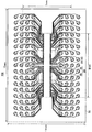
- FIG. 2 is a plan view showing a schematic overall configuration of the semiconductor device of FIG. 1.
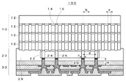
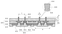
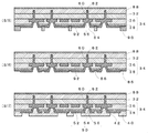
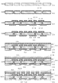
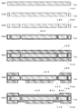
- 1 is a cross-sectional view showing a schematic configuration of a semiconductor device according to a first embodiment. It is sectional drawing which shows schematic structure of the interposer concerning 1st Embodiment. It is drawing which shows schematically the manufacturing method of the interposer of FIG.
- FIG. 5 is a diagram schematically illustrating a method of manufacturing the interposer of FIG. 3, schematically illustrating a subsequent process of FIG. 4.
- FIG. 6 is a diagram schematically illustrating a method of manufacturing the interposer of FIG. 3, schematically illustrating a subsequent process of FIG. 5. It is sectional drawing which shows schematic structure of the interposer concerning 2nd Embodiment.
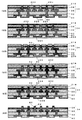
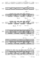
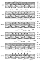
- FIG. 19 is a diagram illustrating a method for manufacturing a multilayer wiring board according to a fourth embodiment, and is a diagram illustrating a subsequent process of FIG. 18. It is sectional drawing which shows the structure of the multilayer wiring board which concerns on 5th Embodiment. It is drawing which shows the manufacturing method of the multilayer wiring board which concerns on 5th Embodiment.
- FIG. 19 is a diagram illustrating a method for manufacturing a multilayer wiring board according to a fourth embodiment, and is a diagram illustrating a subsequent process of FIG. 18. It is sectional drawing which shows the structure of the multilayer wiring board which concerns on 5th Embodiment. It is drawing which shows the manufacturing method of the multilayer wiring board which concerns on 5th Embodiment.
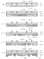
- FIG. 22 is a diagram illustrating a method for manufacturing a multilayer wiring board according to a fifth embodiment, and is a diagram illustrating a subsequent process of FIG. 21. It is sectional drawing which shows the structure of the multilayer wiring board which concerns on 6th Embodiment. It is drawing which shows the manufacturing method of the multilayer wiring board which concerns on 6th Embodiment. It is drawing which shows the manufacturing method of the multilayer wiring board which concerns on 6th Embodiment, Comprising: It is drawing which shows the subsequent process of FIG. It is drawing which shows the manufacturing method of the multilayer wiring board which concerns on 6th Embodiment, Comprising: It is drawing which shows the subsequent process of FIG.
- the present invention can be regarded as an invention related to a multilayer wiring board, and can also be regarded as a manufacturing method and a semiconductor device for manufacturing the multilayer wiring board. Therefore, in the following, for each embodiment, first, the configuration of the semiconductor device will be described, the configuration of the multilayer wiring board will be specifically described, and the method for manufacturing the multilayer wiring board will be further described.
- the semiconductor device (100) is a semiconductor package having a so-called TSV (Through Silicon Via) structure, and mainly includes a semiconductor chip stacked body 10, a controller 20, and an interposer 30 as shown in FIG.
- TSV Three Silicon Via
- the semiconductor chip laminate 10 is formed by laminating a plurality of Si semiconductor chips 12.
- Each semiconductor chip 12 functions as a DRAM (Dynamic Random Access Memory).
- Each semiconductor chip 12 is formed with a through hole 14 (Via), and a through electrode 16 is formed through the through hole 14.
- Each semiconductor chip 12 is electrically connected to another semiconductor chip 12 and the controller 20 through the through electrode 16.
- the controller 20 has a semiconductor chip 22 made of Si.
- a through hole 24 (Via) is also formed in the semiconductor chip 22, and a through electrode 26 is formed through the through hole 24.
- the semiconductor chip 22 is sealed with an underfill 28.
- the controller 20 is electrically connected to the semiconductor chip stack 10 and the interposer 30 through the through electrode 26.
- the interposer 30 is a wiring board for expanding the pitch of the electrodes of the semiconductor chip 22.
- the interposer 30 is a so-called solder bump interposer in which bumps are formed on a flexible flexible substrate.
- the interposer 30 has a resin substrate 32 as a base.
- substrate 32 is comprised from the polyimide resin, the phenol resin, the epoxy resin, the polyester resin, the fluororesin etc., for example, Preferably it is comprised from the polyimide resin.
- the insulating layer 34 is formed below the substrate 32.
- the insulating layer 34 is composed of an adhesive layer 36 and a reinforcing film 38.
- the adhesive layer 36 is made of, for example, an epoxy adhesive or a polyimide adhesive, and is preferably made of an epoxy adhesive.
- the reinforcing film 38 is made of, for example, a polyimide resin film.
- An insulating layer 40 is formed below the insulating layer 34.
- the insulating layer 40 is a layer formed from a solder resist.
- a wiring pattern 50 having a three-dimensional structure is formed on the substrate 32 from the adhesive layer 36 to the insulating layer 40 of the insulating layer 34.
- the wiring pattern 50 is made of a metal whose main component is copper.
- the “metal having copper as a main component” may be copper alone or an alloy in which nickel, cobalt, iron or the like is added to copper.
- the amount of nickel or the like added to copper is preferably 20% or less.
- the wiring pattern 50 is mainly composed of a lower wiring portion 52, a connecting wiring portion 54, and an upper wiring portion 56. In order to make the following description easy to understand, the wiring pattern 50 is divided into these parts, but these parts are actually formed integrally.
- the lower wiring part 52 is covered with the insulating layer 40.
- the insulating layer 40 is patterned in a predetermined pattern, and a part of the lower wiring portion 52 is exposed from the opening 42 of the insulating layer 40.
- the exposed portion of the lower wiring portion 52 functions as an external connection electrode, solder balls or the like are formed on the exposed portion, and the semiconductor device 100 is mounted on a circuit board such as a motherboard.
- the connecting wiring part 54 is formed so as to penetrate the reinforcing film 38.
- the connecting wiring part 54 is connected to the lower wiring part 52 and the upper wiring part 56 and connects these wiring parts.
- the upper wiring part 56 is formed in the adhesive layer 36.
- a post 60 is formed on the upper wiring portion 56.
- the post 60 is erected on the wiring pattern 50 while penetrating the substrate 32.
- the front end portion (top portion 64) of the post 60 is slightly exposed from the substrate 32.
- the substrate 32 covers the side surface of the post 60 in a state where the tip end portion (top portion 64) of the post protrudes, and functions as a protective layer for protecting the post 60.
- a solder bump 62 is formed on the post 60.
- the solder bump 62 is a protruding electrode for electrically flip-chip connection with an electronic device such as a semiconductor chip, and is made of, for example, a tin-silver alloy.
- the post 60 has a tapered shape (reverse taper shape) from the top 64 toward the base 66.
- the top part 64 is a part connected to the semiconductor chip 22 of the controller 20 via the solder bumps 62.
- the base 66 is a part connected to the upper wiring part 56 of the wiring pattern 50.
- the diameter of the top portion 64 is +10 to 20 ⁇ m with respect to the diameter of the electrode 29 (see FIG. 2, described later) of the semiconductor chip 22, and the diameter of the base portion 66 is ⁇ 10 ⁇ m with respect to the diameter of the electrode 29 of the semiconductor chip 22. is there.
- the top portion 64 of the post 60 has a larger area when viewed in plan than the base portion 66, and can prevent displacement between electrodes when connected to the semiconductor chip 22.
- the base portion 66 of the post 60 has a smaller area when viewed in plan than the top portion 64.
- a base metal layer is formed at the interface between the substrate 32, the insulating layer 34, the insulating layer 40, and the wiring pattern 50, or at the interface between the substrate 32 and the post 60.
- the adhesion of the wiring pattern 50 and the post 60 to the substrate 32 is improved.
- the base metal layer is made of, for example, a nickel chromium alloy or copper.
- the package size (interposer 30) is 11 mm ⁇ 15 mm.
- the chip size (semiconductor chip 12) is 7 mm ⁇ 8 mm.
- the diameter a of the through electrode 16 is 20 ⁇ m.
- the pitch b between the through electrodes 16 is 35 ⁇ m.
- the diameter c of the through electrode 26 is 20 ⁇ m.
- the pitch d between the through electrodes 26 is 70 ⁇ m.
- the diameter e of the post 60 is approximately 20 ⁇ m.
- the pitch f between the solder bumps 62 is 70 ⁇ m.
- a pitch g between the external connection electrodes (solder balls) is 800 ⁇ m.
- the height h of the solder bump 62 is 5 ⁇ m.
- the height i of the post 60 is 35 ⁇ m.
- the thickness j of the substrate 32 is 25 ⁇ m.
- the height k of the connecting wiring portion 54 of the wiring pattern 50 is 38 ⁇ m.
- the pitch b between the through electrodes 16 of the semiconductor chip 12 is expanded from 35 ⁇ m to 70 ⁇ m by the controller 20 (semiconductor chip 22), and the pitch d between the through electrodes 26 of the semiconductor chip 22 is increased.
- 30 greatly expands from 70 ⁇ m to 800 ⁇ m.
- the controller 20 (semiconductor chip 22) has an electrode 29 protruding from the bottom surface toward the interposer 30 side.
- the total H (see FIG. 2) of the height of the electrode 29 of the semiconductor chip 22 and the height of the post 60 of the interposer 30 is preferably 35 ⁇ m or more, and more preferably 50 ⁇ m or more.
- either the electrode 29 of the semiconductor chip 22 or the post 60 of the interposer 30 may be higher, but preferably the post 60 is raised to secure the height of the post 60 by 35 ⁇ m or more.
- the post 60 is raised to secure the height of the post 60 by 35 ⁇ m or more.
- the electrode 29 of the semiconductor chip 22 is composed only of the pad electrode, and no bump or the like is formed on the electrode 29.
- the interposer 30 is manufactured by a roll-to-roll method in which a long substrate 32 wound around a predetermined roll is conveyed so as to be wound around another roll, and the wiring pattern 30 and the like are formed in the conveyance process. .
- a dry film 70 made of resin is laminated on the substrate 32, and the dry film 70 is cured by exposure (S1). Thereafter, a through hole 72 is formed at a predetermined position of the substrate 32 and the dry film 70 using a laser, and the smear (scraped) is removed (S2).
- metal is sputtered on the substrate 32 and the dry film 70 to form the metal underlayer 74 (S3).
- a resin dry film 76 is laminated on the metal base layer 74 on the lower surface side of the substrate 32, and the dry film 76 is exposed and developed using a mask having a pattern corresponding to the upper wiring portion 56. Cover with a resin layer (dry film 76) of a predetermined pattern (S4).
- the metal base layer 74 exposed from the dry film 76 is plated with a metal containing copper as a main component to form a metal layer 78 on the metal base layer 74 and the through hole 72 is also filled with the metal layer 79. (S5).
- a resin dry film 80 is attached on the metal layer 78 and the dry film 76 on the lower surface side of the substrate 32, and the metal base layer 74 and the metal layer 78 on the upper surface side of the dry film 70 are removed by etching (S6). ).
- a post 60 composed of the metal layer 79 is formed.
- the laser output is adjusted and gradually lowered from above to form the through hole 72 in a tapered shape (reverse taper shape).
- a tapered post 60 can be formed (see the enlarged portion in FIG. 3).
- solder is plated on the posts 60 to form solder bumps 62 (S7), and the dry films 70, 76, and 80 formed on the substrate 32 are peeled off (S8).
- a resin dry film 82 is applied to the substrate 32, and the portion of the metal base layer 74 covered with the dry film 76 is removed by etching (S9). As a result, the upper wiring portion 56 of the wiring pattern 50 composed of the metal layer 78 is formed.
- an adhesive is applied to the lower surface side of the substrate 32 to form an adhesive layer 36, a reinforcing film 38 is laminated on the adhesive layer 36, and the upper wiring portion 56 is covered with the insulating layer 34 (S10).
- the adhesive layer 36 is cured by heating, and the dry film 82 is peeled off (S11).
- a through hole 84 is formed using a laser until the upper wiring portion 56 is exposed at a predetermined position of the insulating layer 34, and the smear (scraped) is removed (S12).
- a metal base layer 86 is formed by sputtering a metal on the insulating layer 34, the through hole 84, and the upper wiring portion 56 (S13).
- a dry film 88 made of resin is laminated on the substrate 32, and a dry film 90 made of resin is also laminated on the metal base layer 86, and a mask having a pattern corresponding to the lower wiring portion 52 and the connecting wiring portion 54 is used.
- the dry film 90 is exposed and developed, and the metal base layer 86 is covered with a resin layer (dry film 90) having a predetermined pattern (S14).
- the metal base layer 86 exposed from the dry film 90 is plated with a metal containing copper as a main component, and the metal base layer 86 is formed on the metal base layer 86, the through hole 84, and the upper wiring portion 56.
- the dry film 90 is peeled off (S16).
- the metal base layer 86 covered with the dry film 90 is removed by etching. As a result, the lower wiring portion 52 and the connection wiring portion 54 of the wiring pattern 50 constituted by the metal layer 92 are formed.
- the dry film 88 is peeled off.
- a resin solder resist is laminated on the insulating layer 34, the lower wiring portion 52, and the connecting wiring portion 54 to form the insulating layer 40, and the insulating layer 40 is exposed and developed using a mask having a predetermined pattern (S17). .
- S17 a mask having a predetermined pattern
- an opening 42 is formed in the insulating layer 40, and a part of the lower wiring portion 52 is exposed from the opening 42 (an external connection electrode is formed).
- the interposer 30 can be manufactured through the processes of S1 to S17.
- the post 60 is formed on the interposer 30, and the formed portion is filled with the resin such as the substrate 32 and the underfill 28. Therefore, the semiconductor device 100 is mounted on a circuit board such as a motherboard. In this case, the stress is relieved and the occurrence of reflow cracks can be suppressed.
- the second embodiment is different from the first embodiment in the configuration of the interposer, and other configurations are the same as those in the first embodiment.
- the insulating layer 34 is formed on the upper portion of the substrate 32, and the insulating layer 40 is formed on the lower portion of the substrate 32.
- the post 60 is erected on the upper wiring portion 56 of the wiring pattern 50 in a state of penetrating the insulating layer 34 (particularly the reinforcing film 38).
- the insulating layer 34 covers the side surface of the post 60 in a state where the tip portion (top portion 64) of the post 60 protrudes, and the insulating layer 34 functions as a protective layer for protecting the post 60.
- a method for manufacturing the interposer 200 will be described.
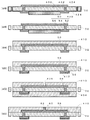
- a through-hole 210 is formed at a predetermined position of the substrate 32 using a laser, and the smear (scratch) is removed (S21). Thereafter, metal is sputtered onto the substrate 32 to form the metal underlayer 212 (S22).
- a metal mainly composed of copper is plated at a predetermined position of the metal base layer 212 to form the metal layer 214 on the metal base layer, and the through hole 210 is also filled with the metal layer 216 (S23).
- the metal base layer 212 exposed from the metal layer 214 is removed by etching (S24). As a result, a wiring pattern 50 composed of the metal layer 214 and the metal layer 216 is formed.
- an adhesive is applied to the upper surface side of the substrate 32 to form an adhesive layer 36, a reinforcing film 38 is laminated on the adhesive layer 36, and the upper wiring portion 56 of the wiring pattern 50 is covered with the insulating layer 34.
- a resin solder resist is laminated on the lower surface side of the substrate 32 to form the insulating layer 40, and the lower wiring portion 52 of the wiring pattern 50 is covered with the insulating layer 40 (S25).
- a resin dry film 218 is stuck on the insulating layer 34 and exposed to cure the dry film 218 (S26).
- a through hole 220 is formed using a laser until the upper wiring portion 56 is exposed at a predetermined position of the dry film 218 and the insulating layer 34, and the lower wiring portion 52 is also formed at a predetermined position of the insulating layer 40 using a laser.
- Through-holes (openings 42) are formed until they are exposed, and these smears (shavings) are removed (S27).
- metal is sputtered on the dry film 218 and the through-hole 220 to form the metal base layer 222, and metal is also sputtered on the insulating layer 40 and the opening 42 to form the metal base layer 224.
- S28 metal is sputtered on the insulating layer 40 and the opening 42 to form the metal base layer 224.
- a resin dry film 226 is affixed to the metal underlayer 224, a metal mainly composed of copper is plated on the metal underlayer 222, a metal layer 228 is formed in the metal underlayer 222, and the through hole 220 is formed.
- the metal layer 230 is filled (S29).
- the metal base layer 222 and the metal layer 228 on the dry film 218 are removed by etching (S30). As a result, the post 60 composed of the metal layer 230 is formed.
- solder is plated on the posts 60 to form solder bumps 62, the dry film 232 is laminated on the solder bumps 62 and the dry film 218, and exposed to cure the dry film 232 (S31).
- the dry film 226 formed on the metal underlayer 224 is peeled off (S32).
- the metal underlayer 224 is removed by etching, and the dry films 218 and 232 on the insulating layer 34 are peeled off simultaneously (S33).
- the interposer 200 can be manufactured through the processes of S21 to S33.
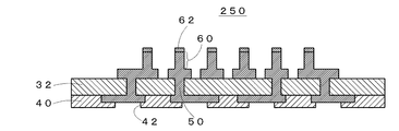
- the interposer 240 in FIG. 10 or the interposer 250 in FIG. 11 may be used.
- an insulating layer 242 is formed instead of the adhesive layer 36 and the reinforcing film 38 of the interposer 200.
- the insulating layer 242 is made of, for example, a polyimide resin.
- the interposer 240 instead of forming the adhesive layer 36 and attaching the reinforcing film 38 in S25, a liquid resin is cast on the substrate 32 and the upper wiring portion 56 and cured. Good.
- the adhesive layer 36 is not formed and the reinforcing film 38 is not pasted in S25, and the dry film 218 is pasted directly on the substrate 32 and the upper wiring portion 26 in S26. That's fine.
- the third embodiment is different from the first embodiment mainly in the following points, and other configurations have the same configurations as those of the first embodiment.
- the semiconductor device 300 is a semiconductor package having a so-called DDP (Double Die Package) structure, in which two semiconductor chips 310 of the same type are stacked and packaged.
- DDP Double Die Package
- the semiconductor device 300 includes a printed circuit board 320 having a size larger than that of the semiconductor chip 310. Bonding pads 322 are formed on the surface of the printed circuit board 320. Electrode pads 324 are formed on the back surface of the printed circuit board 320, and solder balls 326 are formed on the electrode pads 324.
- a semiconductor chip 310 is mounted on the printed circuit board 320 via an adhesive layer 330.
- An electrode 312 is formed on the semiconductor chip 310.
- the electrode 312 is made of, for example, copper, gold, solder, or the like.
- the semiconductor chip 310 is flip-chip connected to the interposer 400 with the electrode 312 facing upward.
- the semiconductor chip 310 and the interposer 400 are further laminated via an adhesive layer 340.
- External connection electrodes 402 are formed outside each interposer 400. Each external connection electrode 402 is electrically connected to the bonding pad 322 of the printed circuit board 320 by a bonding wire 350.
- the semiconductor chips 310 stacked as described above are sealed together with the bonding wires 350 by the sealing resin 360.
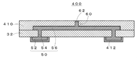
- the interposer 400 is also based on the substrate 32.
- An insulating layer 410 is formed on the substrate 32.
- the insulating layer 410 is made of, for example, an epoxy resin.
- the post 60 is erected on the upper wiring portion 56 of the wiring pattern 50 in a state of penetrating the insulating layer 410.
- the insulating layer 410 covers the side surface of the post 60, and the insulating layer 410 functions as a protective layer for protecting the post 60.
- the lower wiring part 52 of the wiring pattern 50 is covered with a metal layer 412 to form an external connection electrode 402.
- the metal layer 412 has a configuration in which, for example, nickel or gold is laminated.
- the substrate 32 is prepared (S41), and holes 420 for engaging with the transfer roller are opened at predetermined intervals by punching on the side edges of the substrate 32 (S42).
- a through hole 422 is formed at a predetermined position of the substrate 32 by using a laser, and the smear (shaving) is removed and washed (S43). Thereafter, a metal base layer 424 is formed by sputtering metal on the substrate 32 (S44).
- dry films 426 and 428 made of resin are laminated on both surfaces of the substrate 32 (S45), and exposed and developed using a mask having a shape corresponding to the upper wiring portion 56 and the lower wiring portion 52 of the wiring pattern 50 (S46). ). Thereafter, the metal base layer 424 exposed from the dry films 426 and 428 is plated with a metal containing copper as a main component to form the metal layer 430 on the metal base layer 424, and the metal layer 432 is also formed in the through hole 422. Fill (S47).
- the dry films 426 and 428 are peeled off (S48), and the metal base layer 424 covered with the dry films 426 and 428 is removed by etching (S49).
- a wiring pattern 50 (upper wiring portion 56, lower wiring portion 52, and connecting wiring portion 54) composed of the metal layer 430 and the metal layer 432 is formed.
- a resin adhesive (or insulating layer) is attached to the upper surface side of the substrate 32 to form the insulating layer 410 (S50).
- a metal layer 412 is formed by plating the lower wiring portion 52 with a metal (S51).
- a resin dry film 434 is attached to the lower surface side of the substrate 32, and a through hole 436 is formed at a predetermined position of the insulating layer 410 using a laser until the upper wiring portion 56 is exposed. ) Is removed (S52).
- a metal having copper as a main component is plated on the upper wiring portion 56 exposed from the through-hole 436 to form a post 60, and further solder is plated on the post 60 to form a solder bump 62.
- a dry film is formed. 434 is peeled off (S53).
- the interposer 400 can be manufactured through the processes of S41 to S53.
- Sample example (1) Production of Sample A semiconductor device (TSV structure) having the same configuration as that shown in FIG. 2 and a semiconductor device (DPP structure) having the same configuration as that shown in FIG. 12 were manufactured and used as samples.
- TSV structure semiconductor device having the same configuration as that shown in FIG. 2
- DPP structure semiconductor device having the same configuration as that shown in FIG. 12 were manufactured and used as samples.
- the semiconductor device with a package size of 5 mm square and 10 mm square was prepared. While appropriately changing the mode and height of the electrode of the semiconductor chip, the height of the post of the interposer, etc., depending on the combination, samples 1 to 12 (see Table 1), samples 13 to 22 (see Table 2) and Differentiated.
- the height of the post when comparing each sample 1 to 16, in the samples 1 to 8 where the height of the post on the interposer side is 35 ⁇ m or more, there is no occurrence of reflow crack, and in order to prevent the occurrence of reflow crack, the height of the post It can be seen that it is useful to set the thickness to 35 ⁇ m or more.
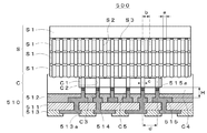
- the semiconductor device 500 of this embodiment is a semiconductor package having a so-called TSV (Through Silicon Via) structure, and as shown in FIG. 16, a multilayer wiring substrate 510, a semiconductor chip stack S, a multilayer wiring substrate 510, and a semiconductor chip. And a controller C disposed between the stacked body S and the laminated body S.
- TSV Three Silicon Via
- the semiconductor chip stack S is formed by stacking a plurality of Si semiconductor chips S1.
- Each semiconductor chip S1 functions as a DRAM (Dynamic Random Access Memory).
- Each semiconductor chip S1 has a through hole S2 (Via), and a through electrode S3 is formed through the through hole S2.
- Each semiconductor chip S1 is electrically connected to another semiconductor chip S1 and the controller C through the through electrode S3.
- the controller C is composed of a Si semiconductor chip C1.
- a through hole C2 (Via) is also formed in the semiconductor chip C1, and a through electrode C3 is formed through the through hole C2 (Via ().
- the semiconductor chip C1 is sealed with underfill C4.
- the controller C is electrically connected to the semiconductor chip stacked body S and the multilayer wiring board 510 through the through electrode C3.
- the multilayer wiring board 510 is a wiring board for expanding the electrode pitch of the semiconductor chip C1.
- the multilayer wiring board 510 is a multilayer wiring board with so-called solder bumps in which bumps are formed on a flexible flexible board.
- the multilayer wiring board 510 has a resin substrate 511 serving as a base.
- the substrate 511 can be formed of any resin such as glass, silicone, polyimide resin, phenol resin, epoxy resin, polyester resin, or fluorine resin. In this embodiment, it is preferable to form with glass, silicone, or a polyimide resin.
- the multilayer wiring board 510 includes an insulating layer 512 on the upper side of the substrate 511 and an insulating layer 513 on the lower side of the substrate 511 in contrast to this. These insulating layers are formed of a polyimide resin, and are formed by building up the substrate 511 by casting (solution casting method).
- one or both of the insulating layers 512 and 513 built up have the same strength in the MD (Machine Direction) direction which is the flow direction of the substrate and in the TD direction (Transverse Direction) which is the vertical direction of the substrate. It becomes possible to do.
- the viscosity that is a precursor of the polyimide resin in order to prevent the generation of voids (laminated voids, that is, the area where there should be no resin or adhesive), the viscosity that is a precursor of the polyimide resin.
- a low-varnish varnish is filled between the circuits, dried, and then a highly viscous varnish is cast.
- This varnish casting (coating and curing) is performed a plurality of times in order to obtain flatness.
- the viscosity of each varnish and the number of castings are appropriately set according to L / S (circuit density), circuit thickness, and CTE inclination.
- the insulating layer formed by such casting maintains adhesion with the wiring pattern and does not cause voids.
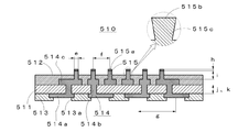
- a wiring pattern 514 having a three-dimensional structure is formed from the insulating layer 512 to the insulating layer 513.
- the wiring pattern 514 is made of a metal whose main component is copper.
- the “metal having copper as a main component” may be copper alone or an alloy in which nickel, cobalt, iron or the like is added to copper. When a metal containing copper as a main component is used as an alloy, the amount of nickel or the like added to copper is preferably 20% or less.
- the wiring pattern 514 mainly includes a lower wiring portion 514a, a connecting wiring portion 514b, and an upper wiring portion 514c. In order to make the following description easy to understand, the wiring pattern 514 is partitioned into these parts, but these parts are actually formed integrally.
- the lower wiring portion 514a is covered with an insulating layer 513.
- the insulating layer 513 is patterned in a predetermined pattern, and a part of the lower wiring portion 514a is exposed from the opening 513a of the insulating layer 513.
- the exposed portion of the lower wiring portion 514a functions as an external connection electrode, solder balls or the like are formed on the exposed portion, and the semiconductor device 500 is mounted on a circuit board such as a motherboard.
- the connecting wiring portion 514b is formed so as to penetrate the insulating layer 513 and the substrate 511, and is connected to the lower wiring portion 514a and the upper wiring portion 514c at the upper and lower end portions to connect these wiring portions.
- the upper wiring portion 514 c is formed in the insulating layer 512.
- a post 515 is formed on the upper wiring portion 514c.
- the post 515 is erected on the wiring pattern 514 while penetrating the insulating layer 512.
- the tip portion (top portion 515 b) of the post 515 is exposed from the insulating layer 512.
- the insulating layer 512 covers the side surface of the post 515 in a state where the tip end portion (top portion 515 b) of the post protrudes, and functions as a protective layer that protects the post 515.
- a solder bump 515 a is formed on the post 515.
- the solder bump 515a is a protruding electrode for electrically flip-chip connection with an electronic device such as a semiconductor chip, and is made of, for example, a tin-silver-copper alloy.
- the post 515 has a tapered shape (reverse taper shape) from the top 515b toward the base 515c.
- the top portion 515b is a portion connected to the semiconductor chip C1 of the controller C through the solder bump 515a.
- the base portion 515 c is a portion connected to the upper wiring portion 514 c of the wiring pattern 514.
- the diameter of the top portion 515b is +10 to 520 ⁇ m with respect to the diameter of the electrode C5 (FIG. 16) of the semiconductor chip C1
- the diameter of the base portion 515c is ⁇ 10 ⁇ m with respect to the diameter of the electrode C5 of the semiconductor chip C1.
- the top portion 515b of the post 515 has a larger area when viewed in plan than the base portion 515c, and can prevent displacement between electrodes when connected to the semiconductor chip C1.
- the base portion 515c of the post 515 has a smaller area when viewed in plan than the top portion 515b.
- a base metal layer is formed at the interface between the substrate 511, the insulating layer 512, the insulating layer 513 and the wiring pattern 514, and the interface between the insulating layer 512 and the post 515.
- Such a base metal layer enhances the adhesion of the wiring pattern 514 and the post 515 to the substrate 511 and the like.
- This base metal layer is made of, for example, a nickel chromium alloy or copper.
- the package size (multilayer wiring board 510) is 11 mm ⁇ 515 mm.
- the chip size (semiconductor chip C1) is 7 mm ⁇ 8 mm.
- the diameter a of the through electrode C3 is 20 ⁇ m.
- the pitch b between the through electrodes C3 is 35 ⁇ m.
- the diameter c of the through electrode C3 is 20 ⁇ m.
- the pitch d between the through electrodes C3 is 70 ⁇ m.
- the diameter e of the post 515 is approximately 20 ⁇ m.
- the pitch f between the solder bumps 515a is 70 ⁇ m.
- a pitch g between the external connection electrodes (solder balls) is 800 ⁇ m.
- the height h of the solder bump 515a is 5 ⁇ m.
- the height i of the post 515 is 35 ⁇ m.
- the thickness j of the substrate 511 is 38 ⁇ m.
- the height k of the connection wiring part 514b of the wiring pattern 514 is 38 ⁇ m.
- the controller C semiconductor chip C1
- the controller C semiconductor chip C1
- an electrode C5 protruding from the bottom surface toward the multilayer wiring board 510 side.
- the total H (see FIG. 16) of the height of the electrode C5 of the semiconductor chip C1 and the height of the post 515 of the multilayer wiring board 510 is preferably 535 ⁇ m or more, more preferably 50 ⁇ m or more.
- either the electrode C5 of the semiconductor chip C1 or the post 515 of the multilayer wiring board 510 may be high, but the post 515 is preferably made high to secure the height of the post 515 of 35 ⁇ m or more.
- the post 515 is preferably made high to secure the height of the post 515 of 35 ⁇ m or more. This is because (i) it is troublesome to manufacture the electrode C5 for each semiconductor chip C1 (for each sheet) to secure the height on the semiconductor chip C1 side, whereas on the multilayer wiring board 510 side This is because the post 515 can be easily manufactured by the roll-to-roll method if the height is to be secured.
- the electrode C5 of the semiconductor chip C1 is composed only of a pad electrode, and no bump or the like is formed on the electrode C5.
- a metal containing copper as a main component is plated at a predetermined position of the metal base layer B1 to form the metal layer ML1 on the metal base layer, and the through hole A1 is also filled with the metal layer ML2 (S3).
- the metal base layer B1 exposed from the metal layer ML1 is removed by etching (S4).
- a wiring pattern 514 (a lower wiring portion 514a, a connecting wiring portion 514b, and an upper wiring portion 514c) composed of the metal layer ML1 and the metal layer ML2 is formed.
- an insulating layer 512 made of polyimide resin is formed on the wiring pattern 514 (upper wiring portion 514 c) on the upper surface side of the substrate 511 by casting, and the upper wiring portion 514 c of the wiring pattern 514 is covered with the insulating layer 512.
- an insulating layer 513 made of polyimide resin is formed on the wiring pattern by casting on the lower surface side of the substrate 511, and the lower wiring portion 514a of the wiring pattern 514 is covered with the insulating layer 513 (S5).
- a low-viscosity varnish that is a polyimide resin precursor is filled between the circuits and dried, and then the high-viscosity is obtained. Cast the varnish. This casting is performed a plurality of times in order to obtain flatness.
- a resin dry film D1 is stuck on the insulating layer 512, and the dry film D1 is cured by exposure (S6).
- a through-hole A2 is formed using a laser until the upper wiring portion 514c is exposed at a predetermined position of the dry film D1 and the insulating layer 512.
- a through hole (opening 513a) is formed at a predetermined position of the insulating layer 513 using a laser until the lower wiring portion 514a is exposed, and these smears are removed (S7).
- metal is sputtered on the dry film D1 and the through hole A2 to form the metal base layer B2, and metal is also sputtered on the insulating layer 513 and the opening 513a to form the metal base layer B3.
- S8 metal is sputtered on the dry film D1 and the through hole A2 to form the metal base layer B2, and metal is also sputtered on the insulating layer 513 and the opening 513a to form the metal base layer B3.
- a dry film D2 made of resin is attached to the metal base layer B3, a metal containing copper as a main component is plated on the metal base layer B2, a metal layer ML3 is formed on the metal base layer B2, and a through hole is further formed.
- A2 is also filled with the metal layer ML4 (S9).
- the metal base layer B2 and the metal layer ML3 on the dry film D1 are removed by etching (S10). As a result, a post 515 composed of the metal layer ML4 is formed.
- solder is plated on the post 515 to form a solder bump 515a
- a dry film D3 is laminated on the solder bump 515a and the dry film D1, and the dry film D3 is cured by exposure (S11).
- the dry film D2 formed on the metal base layer B3 is peeled off (S12).
- the metal base layer B3 is removed by etching, and the dry films D1 and D3 on the insulating layer 512 are simultaneously peeled off (S13).
- the multilayer wiring board 510 can be manufactured through the processes of S1 to S13.
- [4-4. effect] (Board warpage reduction effect)
- the multilayer wiring substrate 510 and the semiconductor device 500 including the multilayer wiring substrate 510 described above by casting, in the insulating layers 512 and 513, the MD direction that is the flow direction of the substrate 511 and the TD direction that is the vertical direction of the substrate 511. And can have the same strength. Therefore, even if the insulating layers 512 and 513 are formed on both surfaces of the substrate 511 by build-up, warpage of the substrate 511 due to this can be reduced. In particular, the warpage of the substrate 511 can be more effectively reduced by configuring all of the insulating layers including the substrate 511 using the same material.
- any or all of the insulating layers 512 and 513 including the substrate 511 in polyimide resin it is possible to provide the multilayer wiring substrate 510 having good heat resistance, a low dielectric constant, and a low linear expansion coefficient.
- the multilayer wiring board 510 made of such a polyimide resin has high rigidity, can be handled in the same way as a glass epoxy board, and becomes a flexible board that does not require a carrier. Therefore, it is possible to cope with conventional transfer equipment, and it is also possible to cope with a reflow method. Furthermore, it is possible to manufacture a multilayer wiring board 510 that is less expensive than an epoxy insulating material.
- the build-up of the insulating layers 512 and 513 is performed by casting (solution casting), so that no physical pressure is applied to the film, so that the orientation of the polymer does not occur, and the strength, optical characteristics, etc. There is no directionality.
- the insulating layer marketed as a film is a standard product and has a predetermined thickness
- an arbitrary thickness can be formed.
- an inclined structure can be produced. Therefore, it is possible to prevent the product from being enlarged due to unnecessary insulating layer thickness.
- the thickness considering signal delay can be arbitrarily set, and a CTE (Linear Expansion Coefficient) material suitable for the circuit density and purpose can be used for the insulating layer, thereby increasing the degree of freedom in design.
- CTE Linear Expansion Coefficient
- the semiconductor package mounting structure is laminated in the order of LSI chip / NCP (Non Conductive Paste) / interposer / underfill / motherboard.
- the CTE is small (3 to 5 ppm) in the LSI chip and large in the mother board. Therefore, in this embodiment, for example, in a semiconductor package, a material having a small CTE is selected on the insulating layer 512 side (LSI chip side) and a material having a large CTE on the insulating layer 513 side (motherboard side) in the multilayer wiring board 510. Select.
- the load on the primary (connection to the LSI chip) and secondary (connection to the motherboard) connection terminals can be reduced. In this way, it is possible to provide the multilayer wiring board 510 with extremely high design freedom.
- the amount of heat applied to the resin is lower than in the melt extrusion molding method (melting like a film-like resin is unnecessary), and the amount of heat stabilizer added can be reduced. Further, the curl condition can be adjusted by setting the melting temperature during casting.
- the insulating layers 512 and 513 having high thickness accuracy and excellent smoothness, transparency and gloss can be formed.
- the fifth embodiment is different from the fourth embodiment in the configuration of the multilayer wiring board, and the other configurations are the same as those in the fourth embodiment. Therefore, the fifth embodiment is different from the fourth embodiment below. Only the point will be described. Further, even in the configuration of the multilayer wiring board, the description in the fourth embodiment is used for points not particularly mentioned.
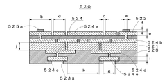
- the multilayer wiring board 520 of this embodiment includes an insulating layer 522 on the upper side of the substrate 521, and includes an insulating layer 523 on the lower side of the substrate 521 in contrast thereto. Similar to the fourth embodiment, these insulating layers are formed of a polyimide resin, and are formed by building up the substrate 521 using casting. Either or both of the insulating layers 522 and 523 thus built up can have the same strength in the MD direction which is the flow direction of the substrate and in the TD direction which is the vertical direction of the substrate.
- a wiring pattern 524 having a three-dimensional structure is formed on the substrate 521 from the insulating layer 522 to the insulating layer 523.
- the wiring pattern 524 mainly includes an uppermost wiring portion 524a, an upper wiring portion 524b, a connection wiring portion 524c, a lower wiring portion 524d, and a lowermost wiring portion 524e.
- the wiring pattern 524 is partitioned into these parts, but these parts are actually formed integrally.
- the lower wiring portion 524d and the lowermost wiring portion 524e are covered with the insulating layer 523, and a part of the lowermost wiring portion 524e is exposed from the opening 523a of the insulating layer 523.
- An exposed portion of the lowermost wiring portion 524e functions as an external connection electrode, solder balls or the like are formed on the exposed portion, and the semiconductor device 500 is mounted on a circuit board such as a motherboard.
- the connecting wiring part 524c is formed so as to penetrate the substrate 521, and is connected to the upper wiring part 524b and the lower wiring part 524d at the upper and lower end parts to connect these wiring parts.
- the upper wiring part 524b is covered with an insulating layer 522, and the uppermost wiring part 524a connected to the upper wiring part 524b is exposed on the upper part of the insulating layer 522.
- the insulating layer 522 is in a state where the uppermost wiring portion 524a is protruded.
- Solder bumps 525 are formed on the uppermost wiring part 524a, and the uppermost wiring part 524a is a part connected to the semiconductor chip C1 of the controller C through the solder bumps 525.
- the solder bump 525 is a protruding electrode for electrically flip-chip connection with an electronic device such as a semiconductor chip, and is made of, for example, a tin-silver-copper alloy.
- the substrate 521, the insulating layer 522, the interface between the insulating layer 523 and the wiring pattern 524, and the base metal layer are formed.
- This base metal layer is made of, for example, a nickel chromium alloy or copper.
- the diameter of the via hole formed in the insulating layer 522 is designed in the range of 15 ⁇ m to 100 ⁇ m.
- the width of the via land is designed to be larger than 160 ⁇ m.
- the space between the uppermost wiring portions 524a is designed to be larger than 15 ⁇ m.
- the line width is designed to be greater than 15 ⁇ m.
- the thickness of the uppermost wiring part 524a is designed to be smaller than 18 ⁇ m.
- the thickness of the solder bump 525 is designed in the range of 2 to 8 ⁇ m.
- the pitch between the openings 523a in the lowermost wiring part 524e is designed to be smaller than 250 ⁇ m.
- the thickness of the lowermost wiring part 524e is designed to be smaller than 18 ⁇ m.
- the thickness of the substrate 521 is designed to be 12.5, 5, 25, 38, 40, or 50 ⁇ m.
- a dry film D1 made of resin is laminated on the metal base layer B1 on the lower surface side of the substrate 521, and the dry film D1 is formed using a mask having a pattern corresponding to the upper wiring portion 524b, the connecting wiring portion 524c, and the lower wiring portion 524d. Formed by exposure and development. Thereby, metal base layer B1 will be coat
- a metal mainly composed of copper is plated at a predetermined position of the metal base layer B1 exposed from the dry film D1, and metal layers ML1 and ML2 are formed on the metal base layer B1 (S4). Thereafter, the dry film D1 and the metal base layer B1 at the position of the dry film D1 are removed by etching (S5). As a result, a part of the wiring pattern 524 composed of the metal layer ML1 and the metal layer ML2 (upper wiring part 524b, connection wiring part 524c, and lower wiring part 524d) is formed.
- polyimide resin is cast as insulating layers 522 and 523 on both the upper surface side and the lower surface side of the substrate 521. Further, a through hole A2 is formed in a predetermined position of the insulating layers 522 and 523 using a laser until the wiring pattern 524 is exposed, and the smear (scratch) is removed (S6). Thereafter, metal is sputtered on the insulating layers 522 and 523 to form the metal base layer B2 (S7).
- a dry film D2 made of resin is stuck on the insulating layers 522 and 523, and the dry film D2 is cured by exposure (S8).
- a metal containing copper as a main component is plated at predetermined positions of the insulating layers 522 and 523 to form metal layers ML3 and ML4 on the insulating layers 522 and 523 (S9).
- the dry film D2 and the metal base layer B2 at the position of the dry film D2 are removed by etching (S10).
- the uppermost wiring part 524a is formed from the metal layer ML3, and the lowermost wiring part 524e is formed from the metal layer ML4.
- a dry film D3 made of resin is laminated on the upper and lower surfaces of the substrate 521 and the wiring portion, and a pattern corresponding to the solder bump 525 is exposed using a mask to cure the dry film D3.
- a solder bump 525 made of tin-silver-copper alloy is formed on the uppermost wiring portion 524a of the wiring pattern 524 provided on the insulating layer 522 (S11).
- the solder bump 525 is a protruding electrode for electrically flip-chip connection with an electronic device such as a semiconductor chip.
- the dry film D3 formed on the substrate 521 is peeled off (S12).
- the multilayer wiring board 520 can be manufactured through the processes of S1 to S13.
- the insulating layer 522 and 523 are built up on the substrate 521, the insulating layer is formed on the wiring pattern 524 by casting.
- the freedom degree of design such as the thickness of an insulating layer
- manufacture of a multilayer substrate can be performed easily. Therefore, the degree of freedom of design in via-on-via or filled via, high-density mounting, interlayer reliability, and layer thickness stability are high, and impedance matching due to flatness can be obtained.
- the connection strength can be improved by using filled vias.
- the sixth embodiment is different from the fourth and fifth embodiments in the configuration of the multilayer wiring board, but the other configurations are the same as those in the fourth and fifth embodiments. Only differences from the fourth and fifth embodiments will be described. In addition, regarding the configuration of the multilayer wiring board, the description in the fourth and fifth embodiments is used for points not particularly mentioned.
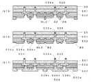
- an insulating layer 532 is formed below a resin substrate 531 serving as a base, and an insulating layer 533 is further formed below the insulating layer 532. Is formed. These insulating layers are formed of a polyimide resin, and are formed by building up the substrate 531 using casting.
- either or both of the insulating layers 532 and 513 are built up in this way, so that the MD (Machine Direction) direction, which is the flow direction of the substrate, and the vertical direction of the substrate are the same.
- the intensity can be made the same in the TD direction (Transverse Direction).
- a wiring pattern 534 having a three-dimensional structure is formed from the insulating layer 532 to the insulating layer 533.
- the wiring pattern 534 mainly includes an upper wiring portion 534a, a connection wiring portion 534b, and a lower wiring portion 534c.
- the wiring pattern 534 is partitioned into these portions, but these portions are actually formed integrally.
- the upper wiring portion 534 a is formed in the insulating layer 532.
- a post 535 is formed on the upper wiring portion 534a.
- the post 535 is erected on the wiring pattern 534 so as to penetrate the substrate 531.
- the front end portion (top portion 535 b) of the post 535 is slightly exposed from the substrate 531.
- the substrate 531 covers the side surface of the post 535 in a state where the tip end portion (top portion 535b) of the post protrudes, and functions as a protective layer for protecting the post 535.
- connection wiring part 534 b is formed so as to penetrate the substrate 531 and the insulating layer 532.
- the connection wiring part 534b is connected to the upper wiring part 534a and the lower wiring part 534c, and connects these wiring parts.
- the lower wiring portion 534c is covered with an insulating layer 533.
- the insulating layer 533 is patterned in a predetermined pattern, and a part of the lower wiring portion 534c is exposed from the opening 533a of the insulating layer 533.
- An exposed portion of the lower wiring portion 534c functions as an external connection electrode.
- a solder ball or the like is formed on the exposed portion, and the semiconductor device 500 is mounted on a circuit board such as a mother board.
- solder bump 535a is formed on the post 535.
- the solder bump 535a is a protruding electrode for electrically flip-chip connection with an electronic device such as a semiconductor chip, and is made of, for example, a tin-silver-copper alloy.
- a base metal layer is formed at the interface between the substrate 531, the insulating layer 532, the insulating layer 533 and the wiring pattern 534, and the interface between the substrate 531 and the post 535.
- a base metal layer enhances the adhesion of the wiring pattern 534 and the post 535 to the substrate 531 and the like.
- This base metal layer is made of, for example, a nickel chromium alloy or copper.
- the package size (multilayer wiring board 530) is 11 mm ⁇ 515 mm.
- the diameter e of the post 535 is approximately 20 ⁇ m.
- the pitch f between the solder bumps 535a is 70 ⁇ m.
- a pitch g between the external connection electrodes (solder balls) is 800 ⁇ m.
- the height h of the solder bump 535a is 5 ⁇ m.
- the height i of the post 535 is 35 ⁇ m.
- the thickness j of the substrate 531 is 25 ⁇ m.
- the height k of the connection wiring part 534b of the wiring pattern 534 is 38 ⁇ m.
- the controller C semiconductor chip C1 is formed with an electrode C5 protruding from the bottom surface toward the multilayer wiring board 530 side.
- the total H (see FIG. 16) of the height of the electrode C5 of the semiconductor chip C1 and the height of the post 535 of the multilayer wiring board 530 is preferably 35 ⁇ m or more, and more preferably 50 ⁇ m or more.
- the multilayer wiring substrate 530 is manufactured by a roll-to-roll method in which a long substrate 531 wound around a predetermined roll is conveyed so that it is wound around another roll, and a wiring pattern 534 and the like are formed in the conveyance process. Is done.
- a dry film D1 made of resin is laminated on a substrate 531 and exposed to cure the dry film D1 (S1). Thereafter, a through-hole A1 is formed at a predetermined position of the substrate 531 and the dry film D1 using a laser, and the smear (shavings) is removed (S2).
- metal is sputtered on the substrate 531 and the dry film D1 to form the metal base layer B1 (S3).
- a dry film D2 made of resin is laminated on the metal base layer B1 on the lower surface side of the substrate 531.
- the dry film D2 is exposed and developed with a pattern corresponding to the upper wiring portion 534a, and the metal base layer B1 is covered with a resin layer (dry film D2) having a predetermined pattern (S4).
- a metal base layer B1 on the dry film D1 and a metal base layer B1 exposed from the dry film D2 are plated with a metal containing copper as a main component to form a metal layer ML1 on the metal base layer B1.
- the metal layer ML2 is filled into the through hole A1 (S5).
- a resin dry film D3 is attached on the metal layer ML1 and the dry film D2 on the lower surface side of the substrate 531, and the metal base layer B1 and the metal layer ML1 on the upper surface side of the dry film D1 are etched and removed (S6). ).
- a post 535 composed of the metal layer ML1 is formed.
- the laser output is adjusted and gradually lowered from the upper side to the lower side, and the through hole A1 is formed in a tapered shape (reverse taper shape).
- a tapered post 535 can be formed (see the enlarged portion in FIG. 23).
- solder is plated on the post 535 to form a solder bump 535a (S7), and the dry films D1, D2, D3 formed on the substrate 531 are peeled off (S8).
- a resin dry film D4 is attached to the substrate 531, and the metal base layer B1 covered with the dry film D2 on the lower surface of the substrate 531 is removed by etching (S9). .
- an upper wiring portion 534a of the wiring pattern 534 composed of the metal layer ML2 is formed.
- the insulating layer 532 is built up on the lower surface side of the substrate 531 by casting, and the upper wiring portion 534a of the wiring pattern 534 is covered with the insulating layer 532 (S10).
- the dry film D4 is peeled off (S11).
- the through-hole A2 is formed using a laser until the upper wiring portion 534a is exposed at a predetermined position of the insulating layer 532, and the smear (scratch) is removed (S12).
- a metal base layer B2 is formed by sputtering metal on the insulating layer 532, the through hole A2, and the upper wiring portion 534a (S13).
- a dry film D5 made of resin is laminated on the substrate 531.
- a dry film D6 made of resin is laminated on the metal base layer B2. Then, the dry film D6 is exposed and developed using a mask having a pattern corresponding to the lower wiring portion 534c and the connecting wiring portion 534b, and the metal base layer B2 is covered with a resin layer (dry film D6) having a predetermined pattern (S14).
- the metal base layer B2 exposed from the dry film D6 is plated with a metal mainly composed of copper, and the metal layer ML2 is formed on the metal base layer B2, the through hole A2, and the upper wiring portion 534a.
- the dry film D6 is peeled off (S16).
- the metal base layer B2 covered with the dry film D6 is removed by etching.
- the lower wiring portion 534c and the connection wiring portion 534b of the wiring pattern 534 composed of the metal layer ML2 are formed.
- the dry film D5 is peeled off, and the insulating layer 532, the lower wiring portion 534c and the connection wiring portion 534b are formed with an insulating layer 533 by casting with polyimide resin without using a solder resist, and using a laser, By forming the opening 533a in the insulating layer 533, a part of the lower wiring portion 534c is exposed from the opening 533a (an external connection electrode is formed) (S17).
- the multilayer wiring board 530 can be manufactured through the processes of S1 to S17.
- the insulating layers 532 and 533 are built up on the substrate 531, so that the MD direction that is the flow direction of the substrate 531, The strength can be made the same in the TD direction which is the vertical direction of the substrate 531. Thereby, the curvature of the substrate 531 can be reduced. In particular, the warpage of the substrate 531 can be more effectively reduced by configuring all the insulating layers including the substrate 531 with the same material.
- the substrate 531 By forming any or all of the insulating layers 532 and 533 including the substrate 531 on a polyimide resin, the substrate 531 having good heat resistance, a low dielectric constant, and a low linear expansion coefficient can be provided. Further, by using polyimide resin and not using an epoxy insulating material and a solder resist, it becomes possible to achieve good heat resistance, low dielectric constant and low linear expansion coefficient, and the substrate 531 has a large size. There is no mounting deviation.
- the insulating layers 532 and 533 are built up by casting, no physical pressure is applied to the film, so that no orientation of the polymer occurs, and there is no directionality in strength, optical characteristics, and the like.
- a first aspect of the present invention includes a resin-made substrate serving as a base, a wiring pattern formed on the substrate, and an insulating layer covering a part of the wiring pattern.
- a post composed of a metal having copper as a main component, a post connected to a semiconductor chip is erected, and the post is erected on the wiring pattern in a state of penetrating the substrate.
- a featured wiring board is provided.
- the wiring pattern includes: a resin substrate serving as a base; a wiring pattern formed on the substrate; and an insulating layer covering a part of the wiring pattern.
- a post composed of a metal having copper as a main component is connected to a semiconductor chip, and the post is erected on the wiring pattern in a state of penetrating the insulating layer.
- a wiring board is provided.
- the step of forming the first through hole at a predetermined position of the resin substrate, the step of forming the first metal base layer on the substrate, and the one surface side of the substrate A step of coating the first metal underlayer with a first resin layer having a predetermined pattern, and a first main component of which is copper as the first metal underlayer exposed from the first resin layer.
- a step of forming a first through hole at a predetermined position of a resin substrate, a step of forming a first metal underlayer on the substrate, and the first metal Forming a first metal layer having a predetermined pattern mainly composed of copper on the underlayer, removing the first metal underlayer exposed from the first metal layer, and removing the first metal layer from the first metal layer.
- a method of manufacturing a wiring board is provided.
- the semiconductor chip in the semiconductor device in which a plurality of semiconductor chips having through electrodes are stacked on the wiring board of the first aspect or the second aspect, includes the semiconductor chip.
- An electrode connected to the wiring board is formed, and the total of the height of the post of the wiring board and the height of the electrode of the semiconductor chip is 35 ⁇ m or more.
- the semiconductor chip in the semiconductor device in which a plurality of semiconductor chips are mounted on the wiring substrate of the first aspect or the second aspect, one by one, includes the semiconductor chip.
- An electrode connected to the wiring board is formed, and the total of the height of the post of the wiring board and the height of the electrode of the semiconductor chip is 35 ⁇ m or more.
- a resin-made substrate serving as a base, a wiring pattern formed on the substrate, and a symmetrical build-up on both surfaces of the substrate are formed while covering the wiring pattern.
- a method for manufacturing a multilayer wiring board according to the seventh aspect wherein the first through hole is formed at a predetermined position of the resin substrate, and the upper and lower surfaces of the substrate. Forming a first metal underlayer on the first metal underlayer, forming a first metal layer mainly composed of copper at a predetermined position of the first metal underlayer, and mainly forming copper in the first through hole.
- the MD (Machine Direction) direction which is the flow direction of the substrate and the TD direction (Transverse Direction) which is the vertical direction of the substrate are set to the same strength. Accordingly, it is possible to provide a flat multilayer wiring board with less warping even when an insulating layer is built up on the board.
- the upper and lower surfaces of the substrate have a vertically symmetrical structure, there is no warpage of the substrate, and at the same time, low thermal expansion can be realized. Even if the substrate is a large size, mounting displacement does not occur.
- a ninth aspect of the present invention is characterized in that, in the seventh aspect, the insulating layer is formed by casting.
- the build-up of the insulating layer is performed by casting (solution casting method), so that no physical pressure is applied to the film, so that the orientation of the polymer does not occur.
- the insulating layer marketed as a film is a standard product and has a predetermined thickness, it can be formed to an arbitrary thickness by casting the insulating layer as described above, and for example, an inclined structure is also produced. Is possible. Therefore, it is possible to prevent the product from being enlarged due to unnecessary insulating layer thickness.
- the thickness considering signal delay can be arbitrarily set, and a CTE (Linear Expansion Coefficient) material suitable for the circuit density and purpose can be used for the insulating layer, thereby increasing the degree of freedom in design.
- CTE Linear Expansion Coefficient
- a tenth aspect of the present invention is characterized in that, in the seventh or eighth aspect, both the substrate and the insulating layer are made of a polyimide resin.
- any or all of the insulating layer including the substrate By forming any or all of the insulating layer including the substrate with a polyimide resin, it is possible to provide a multilayer wiring substrate having good heat resistance, a low dielectric constant, and a low linear expansion coefficient. Also, by using polyimide resin and not using epoxy insulating material and solder resist, it becomes possible to achieve good heat resistance, low dielectric constant and low linear expansion coefficient, and there is no mounting deviation even on a large board .
- a multilayer wiring board made of such a polyimide resin has high rigidity, can be handled in the same manner as a conventional glass epoxy board, and becomes a flexible board that does not require a carrier. Therefore, it is possible to cope with conventional transfer equipment, and it is also possible to cope with a reflow method. Furthermore, an inexpensive multilayer wiring board can be manufactured as compared with an epoxy-based insulating material.
- a semiconductor device including the multilayer wiring board according to the seventh or eighth aspect, the semiconductor chip stacked body, and the multilayer wiring according to the seventh or eighth aspect. It is comprised from a board
- SYMBOLS 10 Semiconductor chip laminated body 12 ... Semiconductor chip 14 ... Through-hole 16 ... Through-electrode 20 ... Controller 22 ... Semiconductor chip 24 ... Through-hole 26 ... Through-electrode 28 ... Underfill 30 ... Interposer 32 ... Substrate 34 ... Insulating layer 36 ... Adhesion Agent layer 38 ... Reinforcing film 40 ... Insulating layer 42 ... Opening portion 50 ... Wiring pattern 52 ... Lower wiring portion 54 ... Connecting wiring portion 56 ... Upper wiring portion 60 ... Post 62 ... Solder bump 64 ... Top 66 ... Base 70 ... Dry film 72 ... Through hole 74 ... Metal underlayer 76 ...
- Electrode pad 326 ... Solder balls 330 and 340 ... Adhesive layer 350 ... Bonding wire 360 ... Sealing resin 400 ... Interposer 410 ... Insulating layer 412 ... Metal layer 420 ... Hole 422 ... Through hole 424 ... Metal base layer 426 428 ... Dry films 430, 432 ... Metal layer 434 ... Dry film 500 ... Semiconductor device 510 ... Multilayer wiring substrate 511 ... Substrate 512, 513 ... Insulating layer 513a ... Opening 514 ... Wiring pattern 514a ... Lower wiring portion 514b ... Connection wiring portion 14c ... Upper wiring portion 515 ... Post 515a ... Solder bump 515b ... Top 515c ...
- Base portion 520 Multilayer wiring board 521 ... Substrate 522a, 523 ... Insulating layer 523a ... Opening 524 ... Wiring pattern 524a ... Top wiring portion 524b ... Upper wiring Portion 524c ... Connecting wiring portion 524d ... Lower wiring portion 524e ... Lower wiring portion 525 ... Solder bump 530 ... Multilayer wiring substrate 531 ... Substrate 532a, 533 ... Insulating layer 533a ... Opening portion 534 ... Wiring pattern 534a ... Upper wiring portion 534b ... Connecting wiring portion 534c ... Lower wiring portion 535 ... Post 535a ... Solder bump 535b ... Top portion A1, A2 ... Through hole B1-B3 ...
- Metal base layer C Controller C1 ... Chip C2 ... Through hole C3 ... Through electrode C4 ... Underfill C5 ... Electrodes D1 to D6 ... Dry films ML1 to ML4 ... Metal layer S ... Semiconductor chip laminated body S1... Semiconductor chip S2.
Landscapes
- Production Of Multi-Layered Print Wiring Board (AREA)
Abstract
リフロークラックの発生やエレクトロマイグレーションの発生を抑制する。平坦性によるインピーダンス整合及び設計自由度が高く、高密度実装が可能な配線基板及びその製造方法並びに半導体装置を提供する。インターポーザ30は、ベースとなる樹脂製の基板32と、基板32上に形成された配線パターン50と、配線パターン50の一部を被覆する絶縁層40とを有している。配線パターン50上の所定位置には、銅を主成分とした金属から構成され、半導体チップと接続されるポスト60が立設され、ポスト60が基板32を貫通した状態で配線パターン50上に立設されている。
Description
本発明は配線基板およびその製造方法ならびに半導体装置に関し、特に配線基板の構造に特化した技術に関する。
近年の電子機器の高密度化に伴い、複数枚の半導体チップを積層して3次元実装構造を実現した高密度の半導体装置(半導体パッケージ)が開発されている。このような半導体装置は、例えば、板状又はフィルム状の基板の表面に、集積回路、抵抗器、コンデンサー等の多数の電子部品を固定し、その部品間を配線で接続することで電子回路を構成するものである。
このような半導体装置を形成する多層配線基板として、層毎に積層、穴あけ加工、回路形成などを繰り返す工法にて作製されたビルドアップ基板が普及している。ビルドアップ基板における回路形成過程では、絶縁層を、フィルム状の樹脂をラミネートして形成しているものがある(特許文献1参照)。
また、たとえば、上記の半導体装置の一形態として、複数枚の半導体チップをそれぞれ1つの基板にワイヤーボンディングで接続して積層させ、パッケージ化することがおこなわれている(特許文献2参照)。しかし、センターに電極(パッド)を有する半導体チップを用いるような場合において、各半導体チップと基板とをワイヤーボンディングしようとすると、各半導体チップを接着するための接着剤層により、ワイヤ自体が押し潰されて電気特性が悪くなるという問題がある。
そこで、このような場合に、半導体チップのセンターパッドから外側に再配線をおこなうため(半導体チップの電極のピッチ拡張のため)に「インターポーザ」といわれる配線基板が用いられている。
最近では、インターポーザは半導体パッケージ自体の電気的特性や耐久性を向上させるためにも使用されており、その例が特許文献2,3などに開示されている。特許文献2の技術によれば、半導体チップ(1)間にインターポーザ(11)を挿入し、電源ノイズの問題を解決しようとしている(段落0027~0033,図3など参照)。特許文献3の技術によれば、半導体チップ(5,8)間にインターポーザ(6)を介在させ、耐久性能を評価している(段落0058,段落0065,表3,表4,図2など参照)。
ところで、半導体チップとインターポーザとの電気的な接続は、一般的には、半導体チップまたはインターポーザの少なくとも一方の外部接続電極に対し、単に半田バンプを設けてこれを溶融(リフロー)することによりおこなわれる。このような接続構造では、半田が流れて絶縁層の厚みが確保できず、リフロークラックが生じる可能性がある。さらには、上述した半導体チップの多段化やファインピッチ化に伴い、エレクトロマイグレーションが生じ、半導体チップとインターポーザとの接続部分で抵抗が上がるという可能性もある。
また、近年益々薄型化が進む多層配線基板においては、電子部品を実装する際の取扱い上、基板の剛性を維持することが課題となっており、上記文献における多層配線基板においても、高剛性で取扱いの容易さを狙っている。しかしながら、上記の従来技術では、基板の絶縁層にフィルム状の樹脂をラミネートする際に配向が生じ、配線基板に反りが起きる原因となっていた。
本発明は、以上のような従来技術の課題を解決するために提案されたものであり、その目的は、リフロークラックの発生やエレクトロマイグレーションの発生を抑制することができる配線基板およびその製造方法ならびにそのような配線基板を利用した半導体装置を提供することにある。
また、本発明の他の目的は、平坦性によるインピーダンス整合及び設計自由度が高く、高密度実装が可能な多層配線基板及びその製造方法並びに半導体装置を提供することにある。
上記課題を解決するため、本発明の多層配線基板の好ましい態様では、ベースとなる樹脂製の基板と、前記基板上に形成された配線パターンと、前記配線パターンの一部を被覆する絶縁層とを有し、前記配線パターン上の所定位置には、銅を主成分とした金属から構成され、半導体チップと接続されるポストが立設され、前記ポストが前記基板を貫通した状態で前記配線パターン上に立設されている。
本発明の多層配線基板の他の好ましい態様では、ベースとなる樹脂製の基板と、前記基板上に形成された配線パターンと、前記配線パターンを被覆しつつ、前記基板の両面に対称にビルドアップして形成した絶縁層と、を有し、前記絶縁層は、MD方向及びTD方向において強度が同じである。
以上の態様では、絶縁層において、基板の流れ方向であるMD(Machine Direction )方向と、基板の垂直方向であるTD方向(Transverse Direction )とを、同じ強度に設定した。これにより、基板に絶縁層をビルドアップしても反りの少ない平坦性ある多層配線基板を提供することができる。また、基板の上面と下面において上下対称構造とすることで基板の反りがなく、同時に低熱膨張を実現可能であり、大きなサイズの基板であっても、実装ずれが生じることがない。
好ましくは、上記態様において、前記絶縁層は、キャスティングにより形成したことを特徴とする。この態様では、絶縁層をビルドアップするに当たって、キャスティング(溶液流延法(solution casting))により行うことで、フィルムに物理的な圧力を加えないため高分子の配向が起こらず、強度や光学特性などに方向性が生じない。また、フィルムとして市販されている絶縁層は、規格品で、厚さが決まっているが、上記態様のとおり、絶縁層をキャスティングすることで、任意の厚みを形成でき、また例えば傾斜構造も作製可能である。そのため、不要な絶縁層厚さによる製品の肥大化も防止できる。また、信号の遅延を考慮した厚さを任意に設定することや、絶縁層として回路密度や目的にあったCTE(線膨張係数)の材料を用いることができ、設計の自由度が高まる。
本発明によれば、リフロークラックの発生やエレクトロマイグレーションの発生を抑制することができる。また、平坦性によるインピーダンス整合及び設計自由度が高く、高密度実装が可能な多層配線基板及びその製造方法並びに半導体装置を提供することができる。
以下、図面を参照しながら本発明の好ましい実施形態について説明する。上述の通り、本発明は、多層配線基板に係る発明として捉えることが可能であるとともに、この多層配線基板を作製する製造方法、半導体装置として捉えることも可能である。そこで、以下、実施形態ごとに、まず、半導体装置の構成を説明した上で、多層配線基板の構成を具体的に説明し、さらに、多層配線基板の製造方法について説明することとする。
[1.第1の実施形態]
半導体装置(100)は、いわゆるTSV(Through Silicon Via)構造を有する半導体パッケージであり、図1に示すとおり、主に半導体チップ積層体10、コントローラ20およびインターポーザ30から構成されている。
半導体装置(100)は、いわゆるTSV(Through Silicon Via)構造を有する半導体パッケージであり、図1に示すとおり、主に半導体チップ積層体10、コントローラ20およびインターポーザ30から構成されている。
図2に示すとおり、半導体チップ積層体10は、複数枚のSi製の半導体チップ12が積層され構成されている。各半導体チップ12は、DRAM(Dynamic Random Access Memory)として機能するものである。各半導体チップ12には貫通孔14(Via)が形成されており、貫通孔14を通じて貫通電極16が形成されている。各半導体チップ12は、貫通電極16を通じて他の半導体チップ12やコントローラ20と電気的に接続されている。
コントローラ20は、Si製の半導体チップ22を有している。半導体チップ22にも貫通孔24(Via)が形成されており、貫通孔24を通じて貫通電極26が形成されている。半導体チップ22は、アンダーフィル28により封止されている。コントローラ20は、貫通電極26を通じて半導体チップ積層体10やインターポーザ30と電気的に接続されている。
インターポーザ30は、半導体チップ22の電極のピッチ拡張のための配線基板である。インターポーザ30は、可撓性のフレキシブル基板にバンプが形成されたいわゆる半田バンプ付きインターポーザである。
図3に示すとおり、インターポーザ30は、ベースとなる樹脂製の基板32を有している。基板32は、たとえばポリイミド樹脂、フェノール樹脂、エポキシ樹脂、ポリエステル樹脂、フッ素樹脂などから構成されており、好ましくはポリイミド樹脂から構成される。
基板32の下部には、絶縁層34が形成されている。絶縁層34は、接着剤層36と補強フィルム38とから構成されている。接着剤層36は、たとえばエポキシ系接着剤やポリイミド系接着剤などから構成されており、好ましくはエポキシ系接着剤から構成される。補強フィルム38は、たとえばポリイミド樹脂製のフィルムから構成されている。
絶縁層34の下部には、絶縁層40が形成されている。絶縁層40は、ソルダーレジストから形成された層である。
基板32上には、絶縁層34の接着剤層36から絶縁層40にかけて3次元的構造を有する配線パターン50が形成されている。配線パターン50は、銅を主成分とした金属で構成されている。
「銅を主成分とする金属」とは、銅単体であってもよいし、銅に対してニッケル、コバルト、鉄などが添加された合金であってもよい。銅を主成分とする金属を合金とする場合、銅に対するニッケルなどの添加量は好ましくは20%以下である。
配線パターン50は主に、下部配線部52、連結配線部54および上部配線部56から構成されている。以後の説明をわかりやすくするために、配線パターン50をこれら部位に区画しているが、これら部位は実際には一体に形成されている。
下部配線部52は、絶縁層40に被覆されている。絶縁層40は、所定パターンにパターニングされており、下部配線部52の一部が絶縁層40の開口部42から露出している。下部配線部52の露出部が外部接続電極として機能するようになっており、当該露出部に半田ボールなどが形成され、半導体装置100がマザーボードなどの回路基板に実装される。
連結配線部54は、補強フィルム38を貫通するように形成されている。連結配線部54は、下部配線部52と上部配線部56とに接続され、これら配線部を連結している。
上部配線部56は、接着剤層36中に形成されている。上部配線部56には、ポスト60が形成されている。ポスト60は、基板32を貫通した状態で配線パターン50上に立設されている。ポスト60の先端部(頂部64)は、基板32からわずかに露出している。基板32は、ポストの先端部(頂部64)を突出させた状態でポスト60の側面を被覆しており、ポスト60を保護する保護層として機能している。
ポスト60上には、半田バンプ62が形成されている。半田バンプ62は、半導体チップなどの電子デバイスと電気的にフリップチップ接続するための突起電極であり、たとえばスズ-銀合金から構成されている。
図3拡大部に示すとおり、ポスト60は、頂部64から基部66に向けて先細の形状(逆テーパ状)を呈している。頂部64は、半田バンプ62を介してコントローラ20の半導体チップ22と接続される部位である。基部66は、配線パターン50の上部配線部56と接続された部位である。たとえば、頂部64の径は、半導体チップ22の電極29(図2,後述参照)の径に対し+10~20μmであり、基部66の径は、半導体チップ22の電極29の径に対し±10μmである。
ポスト60がこのような形状を呈するため、ポスト60の頂部64は、基部66より平面視したときの面積が広く、半導体チップ22との接続時における電極間の位置ずれを防止することができる。その一方、ポスト60の基部66は、頂部64より平面視したときの面積が狭く、ポスト60の形成時に上部配線部56との間の位置ずれや、ポスト60が所望の上部配線部56の隣の上部配線部56に誤って接続されるのを防止することができる。
なお、図3では省略しているが、基板32、絶縁層34および絶縁層40と配線パターン50との界面や、基板32とポスト60との界面には、下地金属層が形成されており、配線パターン50やポスト60の基板32などに対する接着性が高められている。当該下地金属層は、たとえばニッケルクロム合金や銅などから構成されている。
以上の構成を有する半導体装置100の各種寸法は、たとえば、下記のとおりに設計されている(図1~図3参照)。
パッケージサイズ(インターポーザ30)は、11mm×15mmである。
チップサイズ(半導体チップ12)は、7mm×8mmである。
貫通電極16の直径aは、20μmである。
貫通電極16間のピッチbは、35μmである。
貫通電極26の直径cは、20μmである。
貫通電極26間のピッチdは、70μmである。
ポスト60の直径eは、ほぼ20μmである。
半田バンプ62間のピッチfは、70μmである。
外部接続電極(半田ボール)間のピッチgは、800μmである。
半田バンプ62の高さhは、5μmである。
ポスト60の高さiは、35μmである。
基板32の厚みjは、25μmである。
配線パターン50の連結配線部54の高さkは、38μmである。
パッケージサイズ(インターポーザ30)は、11mm×15mmである。
チップサイズ(半導体チップ12)は、7mm×8mmである。
貫通電極16の直径aは、20μmである。
貫通電極16間のピッチbは、35μmである。
貫通電極26の直径cは、20μmである。
貫通電極26間のピッチdは、70μmである。
ポスト60の直径eは、ほぼ20μmである。
半田バンプ62間のピッチfは、70μmである。
外部接続電極(半田ボール)間のピッチgは、800μmである。
半田バンプ62の高さhは、5μmである。
ポスト60の高さiは、35μmである。
基板32の厚みjは、25μmである。
配線パターン50の連結配線部54の高さkは、38μmである。
このように半導体装置100によれば、半導体チップ12の貫通電極16間のピッチbがコントローラ20(半導体チップ22)により35μmから70μmに拡張され、半導体チップ22の貫通電極26間のピッチdがインターポーザ30により70μmから800μmに大幅に拡張される。
ここで、半導体装置100において、コントローラ20(半導体チップ22)には底面からインターポーザ30側に向けて突出する電極29が形成されている。この半導体チップ22の電極29の高さとインターポーザ30のポスト60の高さとの合計H(図2参照)は、好ましくは35μm以上であり、さらに好ましくは50μm以上である。
この場合に、半導体チップ22の電極29とインターポーザ30のポスト60とでいずれが高くてもよいが、好ましくはポスト60を高くしてポスト60の高さを35μm以上確保する。これは(i)半導体チップ22側で高さを確保しようとすると、半導体チップ22ごとに(枚葉ごとに)電極29を製造しなければならず手間がかかるのに対し、インターポーザ30側で高さを確保しようとするほうがロールツーロール方式で容易にポスト60を製造することができるからであり、(ii)半導体チップ22とインターポーザ30の歩留まりを考慮すると、インターポーザ30側で高さを確保したほうがトータルの歩留まりがよいからである。
したがって、好ましくは、半導体チップ22の電極29はパッド電極のみから構成し、電極29にはバンプなどを形成しないのがよい。
続いて、インターポーザ30の製造方法について説明する。
インターポーザ30は、所定のロールに巻かれた長尺の基板32が別のロールに巻き取られるように搬送され、その搬送過程で配線パターン30などが形成されるロールツーロール方式により、製造される。
インターポーザ30は、所定のロールに巻かれた長尺の基板32が別のロールに巻き取られるように搬送され、その搬送過程で配線パターン30などが形成されるロールツーロール方式により、製造される。
具体的には、はじめに、図4に示すとおり、基板32に樹脂製のドライフィルム70をラミネートし、露光してドライフィルム70を硬化させる(S1)。その後、レーザを用いて基板32およびドライフィルム70の所定位置に貫通孔72を形成し、そのスミア(削りかす)を除去する(S2)。
その後、基板32およびドライフィルム70に金属をスパッタリングして金属下地層74を形成する(S3)。その後、基板32の下面側の金属下地層74に樹脂製のドライフィルム76をラミネートし、上部配線部56に対応するパターンのマスクを用いてドライフィルム76を露光・現像し、金属下地層74を所定パターンの樹脂層(ドライフィルム76)で被覆する(S4)。
その後、ドライフィルム76から露出している金属下地層74に銅を主成分とする金属をめっきし、金属下地層74に金属層78を形成するとともに、貫通孔72にも金属層79を充填する(S5)。その後、基板32の下面側の金属層78およびドライフィルム76上に樹脂製のドライフィルム80を貼付し、ドライフィルム70の上面側の金属下地層74および金属層78をエッチングして除去する(S6)。その結果、金属層79から構成されるポスト60が形成される。
なお、S2の処理では、レーザの出力を調整して上方から下方にかけて徐々に低下させ、貫通孔72を先細状(逆テーパ状)に形成する。その結果、先細状のポスト60を形成することができる(図3拡大部参照)。
その後、ポスト60に半田をめっきして半田バンプ62を形成し(S7)、基板32に形成されたドライフィルム70,76,80を剥離する(S8)。その後、図5に示すとおり、基板32に樹脂製のドライフィルム82を貼付するとともに、ドライフィルム76で被覆されていた部分の金属下地層74をエッチングして除去する(S9)。その結果、金属層78から構成される配線パターン50の上部配線部56が形成される。
その後、基板32の下面側に接着剤を塗布して接着剤層36を形成し、さらに接着剤層36上に補強フィルム38をラミネートし、上部配線部56を絶縁層34で被覆する(S10)。その後、加熱して接着剤層36を硬化させるとともに、ドライフィルム82を剥離する(S11)。その後、レーザを用いて絶縁層34の所定位置に上部配線部56が露出するまで貫通孔84を形成し、そのスミア(削りかす)を除去する(S12)。
その後、絶縁層34、貫通孔84および上部配線部56に金属をスパッタリングして金属下地層86を形成する(S13)。その後、基板32に樹脂製のドライフィルム88をラミネートするとともに、金属下地層86にも樹脂製のドライフィルム90をラミネートし、下部配線部52および連結配線部54に対応するパターンのマスクを用いてドライフィルム90を露光・現像し、金属下地層86を所定パターンの樹脂層(ドライフィルム90)で被覆する(S14)。
その後、図6に示すとおり、ドライフィルム90から露出している金属下地層86に銅を主成分とする金属をめっきし、金属下地層86、貫通孔84および上部配線部56に金属層92を形成する(S15)。その後、ドライフィルム90を剥離する(S16)。その後、ドライフィルム90で被覆されていた金属下地層86をエッチングして除去する。その結果、金属層92から構成される配線パターン50の下部配線部52および連結配線部54が形成される。
その後、ドライフィルム88を剥離する。その後、絶縁層34、下部配線部52および連結配線部54に樹脂製のソルダーレジストをラミネートして絶縁層40を形成し、所定パターンのマスクを用いて絶縁層40を露光・現像する(S17)。その結果、絶縁層40に開口部42が形成され、下部配線部52の一部が開口部42から露出する(外部接続電極が形成される。)。
以上のS1~S17の処理を経てインターポーザ30を製造することができる。
以上のS1~S17の処理を経てインターポーザ30を製造することができる。
以上の半導体装置100によれば、インターポーザ30にポスト60が形成され、その形成部分が基板32やアンダーフィル28などの樹脂で満たされているから、半導体装置100をマザーボードなどの回路基板に実装しようとした場合に、応力が緩和されリフロークラックの発生を抑制することができる。
さらに、インターポーザ30にポスト60が形成され、コントローラ20の半導体チップ22とインターポーザ30の配線パターン50との間に所定の間隔が確保されるから、エレクトロマイグレーションの発生も抑制することができる。
[2.第2の実施形態]
第2の実施形態は、インターポーザの構成において第1の実施形態と異なるものであり、それ他の構成については、第1の実施形態と同様である。
第2の実施形態は、インターポーザの構成において第1の実施形態と異なるものであり、それ他の構成については、第1の実施形態と同様である。
図7に示すとおり、本実施形態にかかるインターポーザ200では、基板32の上部に絶縁層34が形成され、基板32の下部に絶縁層40が形成されている。
ポスト60は、絶縁層34(特に補強フィルム38)を貫通した状態で配線パターン50の上部配線部56に立設されている。
インターポーザ200では、絶縁層34がポスト60の先端部(頂部64)を突出させた状態でポスト60の側面を被覆しており、絶縁層34はポスト60を保護する保護層として機能している。
続いて、インターポーザ200の製造方法について説明する。
はじめに、図8に示すとおり、レーザを用いて基板32の所定位置に貫通孔210を形成し、そのスミア(削りかす)を除去する(S21)。その後、基板32に金属をスパッタリングして金属下地層212を形成する(S22)。
はじめに、図8に示すとおり、レーザを用いて基板32の所定位置に貫通孔210を形成し、そのスミア(削りかす)を除去する(S21)。その後、基板32に金属をスパッタリングして金属下地層212を形成する(S22)。
その後、金属下地層212の所定位置に銅を主成分とする金属をめっきし、金属下地層に金属層214を形成するとともに、貫通孔210にも金属層216を充填する(S23)。その後、金属層214から露出している金属下地層212をエッチングして除去する(S24)。その結果、金属層214および金属層216から構成される配線パターン50が形成される。
その後、基板32の上面側に接着剤を塗布して接着剤層36を形成し、さらに接着剤層36上に補強フィルム38をラミネートし、配線パターン50の上部配線部56を絶縁層34で被覆する。併せて、基板32の下面側に樹脂製のソルダーレジストをラミネートして絶縁層40を形成し、配線パターン50の下部配線部52を絶縁層40で被覆する(S25)。
その後、絶縁層34上に樹脂製のドライフィルム218を貼付し、露光してドライフィルム218を硬化させる(S26)。その後、レーザを用いてドライフィルム218および絶縁層34の所定位置に上部配線部56が露出するまで貫通孔220を形成するとともに、レーザを用いて絶縁層40の所定位置にも下部配線部52が露出するまで貫通孔(開口部42)を形成し、それらスミア(削りかす)を除去する(S27)。
その後、図9に示すとおり、ドライフィルム218および貫通孔220に金属をスパッタリングして金属下地層222を形成するとともに、絶縁層40および開口部42にも金属をスパッタリングして金属下地層224を形成する(S28)。その後、金属下地層224に樹脂製のドライフィルム226を貼付するとともに、金属下地層222に銅を主成分とする金属をめっきし、金属下地層222に金属層228を形成するとともに、貫通孔220にも金属層230を充填する(S29)。その後、ドライフィルム218上の金属下地層222および金属層228をエッチングして除去する(S30)。その結果、金属層230から構成されるポスト60が形成される。
その後、ポスト60に半田をめっきして半田バンプ62を形成し、半田バンプ62およびドライフィルム218上にドライフィルム232をラミネートし、露光してドライフィルム232を硬化させる(S31)。その後、金属下地層224に形成されたドライフィルム226を剥離する(S32)。その後、金属下地層224をエッチングして除去し、絶縁層34上のドライフィルム218,232を同時に剥離する(S33)。
以上のS21~S33の処理を経てインターポーザ200を製造することができる。
以上のS21~S33の処理を経てインターポーザ200を製造することができる。
なお、インターポーザ200に代えて、図10のインターポーザ240や図11のインターポーザ250を使用してもよい。図10のインターポーザ240では、インターポーザ200の接着剤層36および補強フィルム38に代えて、絶縁層242が形成されている。絶縁層242は、たとえばポリイミド樹脂から構成されている。
インターポーザ240を製造する場合には、S25において接着剤層36を形成して補強フィルム38を貼付するのに代えて、基板32および上部配線部56上に液状の樹脂をキャスティングして硬化させればよい。
図11のインターポーザ250では、インターポーザ200の接着剤層36および補強フィルム38に相当する部材がない。
インターポーザ250を製造する場合には、S25において接着剤層36を形成して補強フィルム38を貼付することはせず、S26において基板32および上部配線部26上に直接的にドライフィルム218を貼付すればよい。
[3.第3の実施形態]
第3の実施形態は、主に下記の点で第1の実施形態と異なっており、それ他の構成は第1の実施形態と同様の構成を有している。
第3の実施形態は、主に下記の点で第1の実施形態と異なっており、それ他の構成は第1の実施形態と同様の構成を有している。
図12に示すとおり、半導体装置300は、いわゆるDDP(Double Die Package)構造を有する半導体パッケージであって、2枚の同種類の半導体チップ310を積層してパッケージしたものである。
半導体装置300は、半導体チップ310よりサイズが大きいプリント基板320を有している。プリント基板320の表面には、ボンディングパッド322が形成されている。プリント基板320の裏面には、電極パッド324が形成され、電極パッド324には半田ボール326が形成されている。
プリント基板320上には、接着剤層330を介して半導体チップ310が実装されている。半導体チップ310には、電極312が形成されている。電極312は、たとえば銅や金、半田などから構成されている。半導体チップ310は、電極312を上方に向けた状態でインターポーザ400にフリップチップ接続されている。インターポーザ400上には、接着剤層340を介してさらに半導体チップ310およびインターポーザ400が積層されている。
各インターポーザ400の外側には、外部接続電極402が形成されている。各外部接続電極402は、ボンディングワイヤ350によりプリント基板320のボンディングパッド322に電気的に接続されている。
半導体装置300では、上述のように積層された半導体チップ310が、ボンディングワイヤ350とともに封止樹脂360により封止されている。
図13に示すとおり、インターポーザ400でも基板32がベースとなっている。基板32上には絶縁層410が形成されている。絶縁層410は、たとえばエポキシ樹脂から構成されている。
ポスト60は、絶縁層410を貫通した状態で、配線パターン50の上部配線部56に立設されている。
インターポーザ400でも、絶縁層410がポスト60の側面を被覆しており、絶縁層410はポスト60を保護する保護層として機能している。
配線パターン50の下部配線部52は、金属層412で被覆され、外部接続電極402を構成している。金属層412は、たとえばニッケルや金などが積層された構成を有している。
続いて、インターポーザ400の製造方法について説明する。
はじめに、図14に示すとおり、基板32を準備し(S41)、基板32の側縁部に対して搬送用ローラに係止するための孔420をパンチングにより所定間隔で開ける(S42)。
はじめに、図14に示すとおり、基板32を準備し(S41)、基板32の側縁部に対して搬送用ローラに係止するための孔420をパンチングにより所定間隔で開ける(S42)。
その後、レーザを用いて基板32の所定位置に貫通孔422を形成し、そのスミア(削りかす)を除去し洗浄する(S43)。その後、基板32に金属をスパッタリングして金属下地層424を形成する(S44)。
その後、基板32の両面に樹脂製のドライフィルム426,428をラミネートし(S45)、配線パターン50の上部配線部56および下部配線部52に対応する形状のマスクを用いて露光し現像する(S46)。その後、ドライフィルム426,428から露出している金属下地層424に銅を主成分とする金属をめっきし、金属下地層424に金属層430を形成するとともに、貫通孔422にも金属層432を充填する(S47)。
その後、図15に示すとおり、ドライフィルム426,428を剥離し(S48)、ドライフィルム426,428に被覆されていた金属下地層424をエッチングして除去する(S49)。その結果、金属層430および金属層432から構成された配線パターン50(上部配線部56、下部配線部52および連結配線部54)が形成される。
その後、基板32の上面側に樹脂製の接着剤(または絶縁層)を貼付して絶縁層410を形成する(S50)。その後、下部配線部52に金属をめっきして金属層412を形成する(S51)。その後、基板32の下面側に樹脂製のドライフィルム434を貼付するとともに、レーザを用いて絶縁層410の所定位置に上部配線部56が露出するまで貫通孔436を形成し、そのスミア(削りかす)を除去する(S52)。その後、貫通孔436から露出する上部配線部56に銅を主成分とする金属をめっきしてポスト60を形成し、さらにポスト60に半田をめっきして半田バンプ62を形成し、最後にドライフィルム434を剥離する(S53)。
以上のS41~S53の処理を経てインターポーザ400を製造することができる。
以上のS41~S53の処理を経てインターポーザ400を製造することができる。
[サンプル例]
(1)サンプルの作製
図2と同様の構成を有する半導体装置(TSV構造)と、図12と同様の構成を有する半導体装置(DPP構造)とを製造して、これらをサンプルとした。
(1)サンプルの作製
図2と同様の構成を有する半導体装置(TSV構造)と、図12と同様の構成を有する半導体装置(DPP構造)とを製造して、これらをサンプルとした。
半導体装置としてパッケージサイズが5mm角のものと10mm角のものとを準備した。半導体チップの電極の態様やその高さ、インターポーザのポストの高さなどを適宜変更しながら、その組み合わせに応じて、サンプル1~12(表1参照),サンプル13~22(表2参照)と区別した。
表1および表2中、サンプル2,4,6,8,10,12,14,16の「(注)」は、半導体チップ側でパッド電極を使用しており、そのパッド電極の半導体チップからの突出長さを表している。
(2)サンプルの評価
(2.1)リフロークラック試験
各サンプルをリフロー処理し、リフロー処理後のクラックの有無を観察した。
観察結果を表1および表2に示す。
表1および表2中、○,△,×の基準は、下記のとおりである。
「○」…5mm角,10mm角ともにクラックがない
「△」…5mm角ではクラックはないが、10mm角では1個以上のパッケージでクラックが発生している
「×」…5mm角,10mm角ともに1個以上のパッケージでクラックが発生している
(2.1)リフロークラック試験
各サンプルをリフロー処理し、リフロー処理後のクラックの有無を観察した。
観察結果を表1および表2に示す。
表1および表2中、○,△,×の基準は、下記のとおりである。
「○」…5mm角,10mm角ともにクラックがない
「△」…5mm角ではクラックはないが、10mm角では1個以上のパッケージでクラックが発生している
「×」…5mm角,10mm角ともに1個以上のパッケージでクラックが発生している
(2.2)長期信頼性試験(エレクトロマイグレーション)
各サンプルにおいて、初期状態と一定環境(110℃,85%RH,1.95V,500時間)に放置した後とで、抵抗値を測定した。抵抗値の増加が10%以内であれば「○」と、10%を上回った場合は「×」と評価した。
評価結果を表1および表2に示す。
各サンプルにおいて、初期状態と一定環境(110℃,85%RH,1.95V,500時間)に放置した後とで、抵抗値を測定した。抵抗値の増加が10%以内であれば「○」と、10%を上回った場合は「×」と評価した。
評価結果を表1および表2に示す。

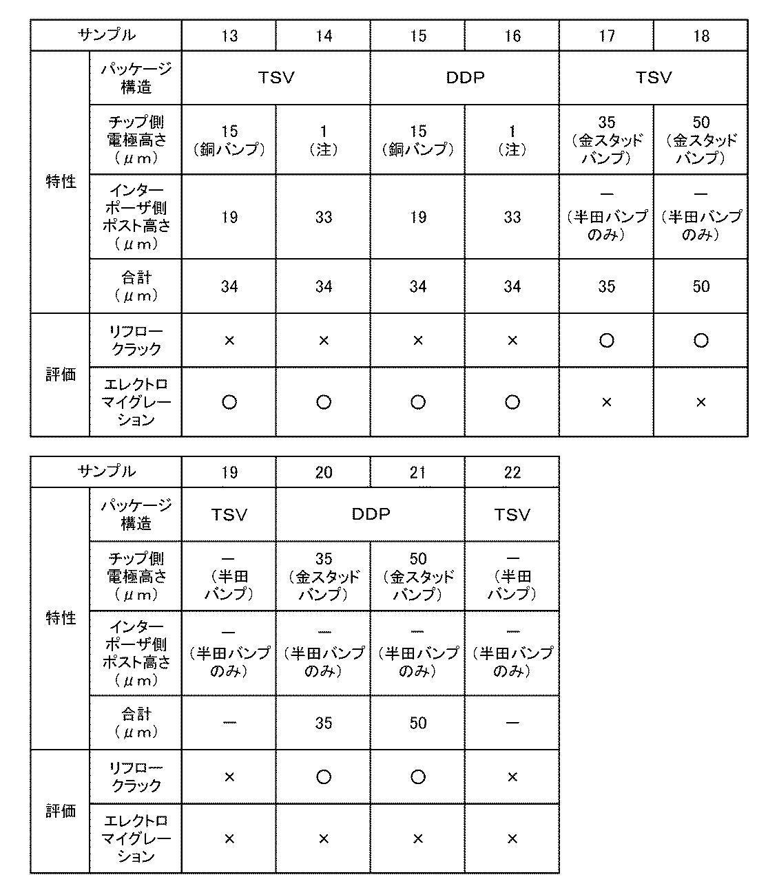
(3)まとめ
表1および表2に示すとおり、サンプル1~16とサンプル17~22とを比較すると、インターポーザ側にポストを形成したサンプル1~16では、長期信頼性試験において良好な結果が得られており、長期信頼性の向上のためには、インターポーザにポストを形成するのが有用であることがわかる。
表1および表2に示すとおり、サンプル1~16とサンプル17~22とを比較すると、インターポーザ側にポストを形成したサンプル1~16では、長期信頼性試験において良好な結果が得られており、長期信頼性の向上のためには、インターポーザにポストを形成するのが有用であることがわかる。
特に、各サンプル1~16を比較すると、インターポーザ側のポストの高さが35μm以上であるサンプル1~8では、リフロークラックの発生もなく、リフロークラックの発生を防止する上では、ポストの高さを35μm以上とするのが有用であることがわかる。
[4.第4の実施形態]
[4-1.半導体装置の構成]
本実施形態の半導体装置500は、いわゆるTSV(Through Silicon Via )構造を有する半導体パッケージであり、図16に示すとおり、多層配線基板510と、半導体チップ積層体Sと、多層配線基板510と半導体チップ積層体Sとの間に配置されるコントローラCと、とから構成される。
[4-1.半導体装置の構成]
本実施形態の半導体装置500は、いわゆるTSV(Through Silicon Via )構造を有する半導体パッケージであり、図16に示すとおり、多層配線基板510と、半導体チップ積層体Sと、多層配線基板510と半導体チップ積層体Sとの間に配置されるコントローラCと、とから構成される。
図16に示すとおり、半導体チップ積層体Sは、複数枚のSi製の半導体チップS1が積層され構成されている。各半導体チップS1は、DRAM(Dynamic Random Access Memory)として機能するものである。各半導体チップS1には貫通孔S2(Via)が形成されており、貫通孔S2を通じて貫通電極S3が形成されている。各半導体チップS1は、貫通電極S3を通じて他の半導体チップS1やコントローラCと電気的に接続されている。
コントローラCは、Si製の半導体チップC1からなる。半導体チップC1にも貫通孔C2(Via)が形成されており、貫通孔C2(Via )を通じて貫通電極C3が形成されている。半導体チップC1は、アンダーフィルC4により封止されている。コントローラCは、貫通電極C3を通じて半導体チップ積層体Sや多層配線基板510と電気的に接続されている。
[4-2.多層配線基板の構成]
多層配線基板510は、半導体チップC1の電極ピッチ拡張のための配線基板である。多層配線基板510は、可撓性のフレキシブル基板にバンプが形成されたいわゆる半田バンプ付き多層配線基板である。
多層配線基板510は、半導体チップC1の電極ピッチ拡張のための配線基板である。多層配線基板510は、可撓性のフレキシブル基板にバンプが形成されたいわゆる半田バンプ付き多層配線基板である。
図16及び図17に示すとおり、多層配線基板510は、ベースとなる樹脂製の基板511を有している。基板511は、たとえばガラス、シリコーン、ポリイミド樹脂、フェノール樹脂、エポキシ樹脂、ポリエステル樹脂、フッ素樹脂など、いかなる樹脂によっても形成可能である。本実施形態においては、ガラス、シリコーン又はポリイミド樹脂により形成するのが好ましい。
多層配線基板510は、基板511の上部に絶縁層512を備え、これと対称に基板511の下部に絶縁層513を備える。これらの絶縁層は、ポリイミド樹脂により形成されており、基板511に対してキャスティング(溶液流延法(solution casting ))によりビルドアップして形成される。
これによりビルドアップされた絶縁層512,513のいずれか又は両方が、基板の流れ方向であるMD(Machine Direction )方向と、基板の垂直方向であるTD方向(Transverse Direction )とにおいて強度を同じにすることが可能となる。
ここで、本実施形態の絶縁層のキャスティングにおいては、ボイド(積層ボイド、すなわち通常あるべきエリアに樹脂又は接着剤がないこと。)の発生を防止するために、ポリイミド樹脂の前駆体である粘度の低いワニスを回路間に充填し乾燥後、粘度の高いワニスをキャスティングする。このワニスのキャスティング(塗布、硬化)は、平坦性を出すために複数回行う。なお、各ワニスの粘度、キャスティング回数は、L/S(回路密度)や回路厚み、CTEの傾斜具合に応じて適宜設定する。このようなキャスティングにより形成される絶縁層は、配線パターンとの密着性を維持し、ボイドを生じさせない。
基板511上には、絶縁層512から絶縁層513にかけて3次元的構造を有する配線パターン514が形成されている。配線パターン514は、銅を主成分とした金属で構成されている。「銅を主成分とする金属」とは、銅単体であってもよいし、銅に対してニッケル、コバルト、鉄などが添加された合金であってもよい。銅を主成分とする金属を合金とする場合、銅に対するニッケルなどの添加量は好ましくは20%以下である。
配線パターン514は主に、下部配線部514a、連結配線部514bおよび上部配線部514cから構成されている。以後の説明を分かり易くするために、配線パターン514をこれら部位に区画しているが、これら部位は実際には一体に形成されている。
下部配線部514aは、絶縁層513に被覆されている。絶縁層513は、所定パターンにパターニングされており、下部配線部514aの一部が絶縁層513の開口部513aから露出している。下部配線部514aの露出部が外部接続電極として機能するようになっており、当該露出部に半田ボールなどが形成され、半導体装置500がマザーボードなどの回路基板に実装される。
連結配線部514bは、絶縁層513及び基板511を貫通するように形成され、上下端部において下部配線部514aと上部配線部514cとに接続され、これら配線部を連結している。
上部配線部514cは、絶縁層512中に形成されている。上部配線部514cには、ポスト515が形成されている。ポスト515は、絶縁層512を貫通した状態で配線パターン514上に立設されている。ポスト515の先端部(頂部515b)は、絶縁層512から露出している。絶縁層512は、ポストの先端部(頂部515b)を突出させた状態でポスト515の側面を被覆しており、ポスト515を保護する保護層として機能している。
ポスト515上には、半田バンプ515aが形成されている。半田バンプ515aは、半導体チップなどの電子デバイスと電気的にフリップチップ接続するための突起電極であり、たとえばスズ-銀-銅合金から構成されている。
図17の拡大部に示すとおり、ポスト515は、頂部515bから基部515cに向けて先細り形状(逆テーパ状)を呈している。頂部515bは、半田バンプ515aを介してコントローラCの半導体チップC1と接続される部位である。基部515cは、配線パターン514の上部配線部514cと接続された部位である。たとえば、頂部515bの径は、半導体チップC1の電極C5(図16)の径に対し+10~520μmであり、基部515cの径は、半導体チップC1の電極C5の径に対し±10μmである。
ポスト515がこのような形状を呈するため、ポスト515の頂部515bは、基部515cより平面視したときの面積が広く、半導体チップC1との接続時における電極間の位置ずれを防止することができる。その一方、ポスト515の基部515cは、頂部515bより平面視したときの面積が狭く、ポスト515の形成時に上部配線部514cとの位置ずれや、ポスト515が所望の上部配線部514cの隣の上部配線部514cに誤って接続されるのを防止することができる。
なお、図17では省略しているが、基板511、絶縁層512および絶縁層513と配線パターン514との界面や、絶縁層512とポスト515との界面には、下地金属層が形成されている。このような下地金属層により、配線パターン514やポスト515の基板511などに対する接着性が高められている。この下地金属層は、たとえばニッケルクロム合金や銅などから構成されている。
以上の構成を有する半導体装置500の各種寸法は、たとえば、下記のとおりに設計されている(図16~図17参照)。
パッケージサイズ(多層配線基板510)は、11mm×515mmである。
チップサイズ(半導体チップC1)は、7mm×8mmである。
貫通電極C3の直径aは、20μmである。
貫通電極C3間のピッチbは、35μmである。
貫通電極C3の直径cは、20μmである。
貫通電極C3間のピッチdは、70μmである。
ポスト515の直径eは、ほぼ20μmである。
半田バンプ515a間のピッチfは、70μmである。
外部接続電極(半田ボール)間のピッチgは、800μmである。
半田バンプ515aの高さhは、5μmである。
ポスト515の高さiは、35μmである。
基板511の厚みjは、38μmである。
配線パターン514の連結配線部514bの高さkは、38μmである。
パッケージサイズ(多層配線基板510)は、11mm×515mmである。
チップサイズ(半導体チップC1)は、7mm×8mmである。
貫通電極C3の直径aは、20μmである。
貫通電極C3間のピッチbは、35μmである。
貫通電極C3の直径cは、20μmである。
貫通電極C3間のピッチdは、70μmである。
ポスト515の直径eは、ほぼ20μmである。
半田バンプ515a間のピッチfは、70μmである。
外部接続電極(半田ボール)間のピッチgは、800μmである。
半田バンプ515aの高さhは、5μmである。
ポスト515の高さiは、35μmである。
基板511の厚みjは、38μmである。
配線パターン514の連結配線部514bの高さkは、38μmである。
ここで、半導体装置500において、コントローラC(半導体チップC1)には底面から多層配線基板510側に向けて突出する電極C5が形成されている。この半導体チップC1の電極C5の高さと多層配線基板510のポスト515の高さとの合計H(図16参照)は、好ましくは535μm以上であり、さらに好ましくは50μm以上である。
この場合に、半導体チップC1の電極C5と多層配線基板510のポスト515とでいずれが高くてもよいが、好ましくはポスト515を高くしてポスト515の高さを35μm以上確保する。これは(i)半導体チップC1側で高さを確保しようとすると、半導体チップC1ごとに(枚葉ごとに)電極C5を製造しなければならず手間がかかるのに対し、多層配線基板510側で高さを確保しようとする方がロールツーロール方式で容易にポスト515を製造することができるからである。また、(ii)半導体チップC1と多層配線基板510の歩留まりを考慮すると、多層配線基板510側で高さを確保したほうがトータルの歩留まりが良いからである。従って、好ましくは、半導体チップC1の電極C5はパッド電極のみから構成し、電極C5にはバンプなどを形成しないのが良い。
[4-3.多層配線基板の製造方法]
続いて、多層配線基板510の製造方法について説明する。
図18に示すとおり、レーザを用いて基板511の所定位置に貫通孔A1を形成し、そのスミア(削りかす)を除去する(S1)。その後、基板511に金属をスパッタリングして金属下地層B1を形成する(S2)。
続いて、多層配線基板510の製造方法について説明する。
図18に示すとおり、レーザを用いて基板511の所定位置に貫通孔A1を形成し、そのスミア(削りかす)を除去する(S1)。その後、基板511に金属をスパッタリングして金属下地層B1を形成する(S2)。
その後、金属下地層B1の所定位置に銅を主成分とする金属をめっきし、金属下地層に金属層ML1を形成するとともに、貫通孔A1にも金属層ML2を充填する(S3)。その後、金属層ML1から露出している金属下地層B1をエッチングして除去する(S4)。その結果、金属層ML1および金属層ML2から構成される配線パターン514(下部配線部514a、連結配線部514bおよび上部配線部514c)が形成される。
その後、基板511の上面側の配線パターン514(上部配線部514c)上にキャスティングにより、ポリイミド樹脂よりなる絶縁層512を形成し、配線パターン514の上部配線部514cを絶縁層512で被覆する。併せて、基板511の下面側にも、配線パターン上にキャスティングによりポリイミド樹脂よりなる絶縁層513を形成し、配線パターン514の下部配線部514aを絶縁層513で被覆する(S5)。
ここで、本実施形態の絶縁層のキャスティングにおいては、上述のとおり、ボイドの発生を防止するために、ポリイミド樹脂の前駆体である粘度の低いワニスを回路間に充填し乾燥後、粘度の高いワニスをキャスティングする。このキャスティングは、平坦性を出すために複数回行う。
その後、絶縁層512上に樹脂製のドライフィルムD1を貼付し、露光してドライフィルムD1を硬化させる(S6)。その後、レーザを用いてドライフィルムD1および絶縁層512の所定位置に上部配線部514cが露出するまで貫通孔A2を形成する。それとともに、レーザを用いて絶縁層513の所定位置にも下部配線部514aが露出するまで貫通孔(開口部513a)を形成し、それらスミア(削りかす)を除去する(S7)。
その後、図19に示すとおり、ドライフィルムD1および貫通孔A2に金属をスパッタリングして金属下地層B2を形成するとともに、絶縁層513および開口部513aにも金属をスパッタリングして金属下地層B3を形成する(S8)。その後、金属下地層B3に樹脂製のドライフィルムD2を貼付するとともに、金属下地層B2に銅を主成分とする金属をめっきし、金属下地層B2に金属層ML3を形成し、さらに、貫通孔A2にも金属層ML4を充填する(S9)。その後、ドライフィルムD1上の金属下地層B2および金属層ML3をエッチングして除去する(S10)。その結果、金属層ML4から構成されるポスト515が形成される。
その後、ポスト515に半田をめっきして半田バンプ515aを形成し、半田バンプ515aおよびドライフィルムD1上にドライフィルムD3をラミネートし、露光してドライフィルムD3を硬化させる(S11)。その後、金属下地層B3に形成されたドライフィルムD2を剥離する(S12)。その後、金属下地層B3をエッチングして除去し、絶縁層512上のドライフィルムD1,D3を同時に剥離する(S13)。
以上のS1~S13の処理を経て多層配線基板510を製造することができる。
以上のS1~S13の処理を経て多層配線基板510を製造することができる。
[4-4.効果]
(基板の反り低減効果)
以上の多層配線基板510及びそれを備えた半導体装置500によれば、キャスティングすることで、絶縁層512,513において、基板511の流れ方向であるMD方向と、基板511の垂直方向であるTD方向とにおいて強度を同じにすることができる。そのため、基板511の両面に絶縁層512,513をビルドアップにより形成したとしても、これによる基板511の反りを低減することができる。特に、基板511を含む絶縁層のすべてを同じ材料により構成することにより、基板511の反りをより効果的に低減することができる。
(基板の反り低減効果)
以上の多層配線基板510及びそれを備えた半導体装置500によれば、キャスティングすることで、絶縁層512,513において、基板511の流れ方向であるMD方向と、基板511の垂直方向であるTD方向とにおいて強度を同じにすることができる。そのため、基板511の両面に絶縁層512,513をビルドアップにより形成したとしても、これによる基板511の反りを低減することができる。特に、基板511を含む絶縁層のすべてを同じ材料により構成することにより、基板511の反りをより効果的に低減することができる。
また、上下絶縁層512及び513を、対称構造とすることで基板511の反りがなく、同時に低熱膨張を実現することができる。そのため、大きなサイズの基板であっても、実装ずれが生じることがない。
(ポリイミド樹脂を用いた効果)
基板511を含む、絶縁層512,513のいずれか又はすべてをポリイミド樹脂に形成することで、良好な耐熱性と低誘電率、低線膨張係数からなる多層配線基板510を提供することができる。また、ポリイミド樹脂を用いて、エポキシ系絶縁材料及びソルダーレジストを使用しないことで、良好な耐熱性、低誘電率及び低線膨張率を実現することが可能となり、基板511が大きな場合でも、実装ずれがない。
基板511を含む、絶縁層512,513のいずれか又はすべてをポリイミド樹脂に形成することで、良好な耐熱性と低誘電率、低線膨張係数からなる多層配線基板510を提供することができる。また、ポリイミド樹脂を用いて、エポキシ系絶縁材料及びソルダーレジストを使用しないことで、良好な耐熱性、低誘電率及び低線膨張率を実現することが可能となり、基板511が大きな場合でも、実装ずれがない。
このようなポリイミド樹脂により作製した多層配線基板510は、剛性が高く、ガラスエポキシ基板と同様の扱いが可能で、キャリア不要なフレキシブル基板となる。そのため、従来の搬送設備にて対応が可能で、リフロー方式にも対応することができる。さらに、エポキシ系絶縁材料に比較して、安価な多層配線基板510を作製することができる。
(配線パターン上にキャスティングで絶縁層を形成する効果)
絶縁層512,513をビルドアップするに当たって、キャスティング(溶液流延法(solution casting))により行うことで、フィルムに物理的な圧力を加えないため高分子の配向が起こらず、強度や光学特性などに方向性が生じない。
絶縁層512,513をビルドアップするに当たって、キャスティング(溶液流延法(solution casting))により行うことで、フィルムに物理的な圧力を加えないため高分子の配向が起こらず、強度や光学特性などに方向性が生じない。
また、フィルムとして市販されている絶縁層は、規格品で、厚さが決まっているが、本実施形態のように、絶縁層512,513をキャスティングすることで、任意の厚みを形成でき、また例えば傾斜構造も作製可能である。そのため、不要な絶縁層厚さによる製品の肥大化も防止できる。また、信号の遅延を考慮した厚さを任意に設定することや、絶縁層として回路密度や目的にあったCTE(線膨張係数)の材料を用いることができ、設計の自由度が高まる。
半導体パッケージ実装構造は、上述のように、LSIチップ/NCP(Non Conductive Paste )/インターポーザー/アンダーフィル/マザーボードの順で積層されている。このうち、LSIチップにおいてCTEは小さく(3~5ppm)、マザーボードにおいて大きい。そこで、本実施形態では、例えば、半導体パッケージでは、多層配線基板510において、絶縁層512側(LSIチップ側)にCTEの小さい材料を選択し、絶縁層513側(マザーボード側)にCTEの大きい材料を選択する。これにより、1次(LSIチップとの接続)、2次(マザーボードとの接続)接続端子への負荷を軽減できる。このように設計の自由度が極めて高い多層配線基板510を提供することができる。
また、キャスティングでは、溶融押出成型法に比べ樹脂にかける熱量が低く(フィルム状樹脂のような溶融も不要)、熱安定剤などの添加量を低減できる。また、キャスティング時の溶融温度の設定によりカール具合を調整することができる。
また、このようなキャスティングにより、溶液をろ過する工程を設置できるため樹脂の塊(フィッシュアイ)が発生せず、キズもつきにくいため、絶縁層512,513に用いるための透明性の高いフィルムを成型できる。
このように、絶縁層512,513の成形にキャスティングを用いることで、厚み精度が高く、平滑性、透明性、光沢性に優れた絶縁層512,513を形成できるといったメリットがある。なお、このようにキャスティングを用いることで、融点が高く押出成形が難しいポリイミドフィルムによって絶縁層512,513を形成することが容易となる。
[5.第5の実施形態]
第5の実施形態は、多層配線基板の構成において第4の実施形態と異なるものであり、その他の構成については、第4の実施形態と同様であるので、以下では第4の実施形態と異なる点についてのみ説明する。また、多層配線基板の構成であっても、特に言及しない点については、第4の実施形態における説明を援用するものとする。
第5の実施形態は、多層配線基板の構成において第4の実施形態と異なるものであり、その他の構成については、第4の実施形態と同様であるので、以下では第4の実施形態と異なる点についてのみ説明する。また、多層配線基板の構成であっても、特に言及しない点については、第4の実施形態における説明を援用するものとする。
[5-1.多層配線基板の構成]
図20に示すとおり、本実施形態の多層配線基板520は、基板521の上部に絶縁層522を備え、これと対称に基板521の下部に絶縁層523を備える。これらの絶縁層は、第4の実施形態と同様、ポリイミド樹脂により形成されており、基板521に対してキャスティングを用いてビルドアップして形成される。このようにビルドアップされた絶縁層522,523のいずれか又は両方が、基板の流れ方向であるMD方向と、基板の垂直方向であるTD方向とにおいて強度を同じにすることができる。
図20に示すとおり、本実施形態の多層配線基板520は、基板521の上部に絶縁層522を備え、これと対称に基板521の下部に絶縁層523を備える。これらの絶縁層は、第4の実施形態と同様、ポリイミド樹脂により形成されており、基板521に対してキャスティングを用いてビルドアップして形成される。このようにビルドアップされた絶縁層522,523のいずれか又は両方が、基板の流れ方向であるMD方向と、基板の垂直方向であるTD方向とにおいて強度を同じにすることができる。
基板521上には、絶縁層522から絶縁層523にかけて3次元的構造を有する配線パターン524が形成されている。配線パターン524は主に、最上部配線部524a、上部配線部524b、連結配線部524c、下部配線部524dおよび最下部配線部524eから構成されている。ここでは、第4の実施形態と同様、説明の便宜上、配線パターン524をこれら部位に区画しているが、これら部位は実際には一体に形成されている。
下部配線部524d及び最下部配線部524eは、絶縁層523に被覆され、最下部配線部524eの一部が絶縁層523の開口部523aから露出している。最下部配線部524eの露出部が外部接続電極として機能するようになっており、当該露出部に半田ボールなどが形成され、半導体装置500がマザーボードなどの回路基板に実装される。
連結配線部524cは、基板521を貫通するように形成され、上下端部において上部配線部524bと下部配線部524dとに接続され、これら配線部を連結している。
上部配線部524bは絶縁層522に被覆されており、この上部配線部524bと接続した最上部配線部524aは、絶縁層522の上部に露出して配置されている。絶縁層522は、最上部配線部524aを突出させた状態となっている。
最上部配線部524a上には、半田バンプ525が形成され、最上部配線部524aは、半田バンプ525を介してコントローラCの半導体チップC1と接続される部位である。半田バンプ525は、半導体チップなどの電子デバイスと電気的にフリップチップ接続するための突起電極であり、たとえばスズ-銀-銅合金から構成されている。
なお、第4の実施形態と同様、基板521、絶縁層522および絶縁層523と配線パターン524との界面や、下地金属層が形成されている。このような下地金属層により、配線パターン524の基板521などに対する接着性が高められている。この下地金属層は、たとえばニッケルクロム合金や銅などから構成されている。
以上の構成を有する多層配線基板520の各種寸法は、たとえば、下記のとおりに設計されている(図20参照)。
(a)絶縁層522に形成されたビアホールの直径は、15μm~100μmの範囲で設計される。
(b)ビアランドの幅は、160μmより大きく設計される。
(c)最上部配線部524a間のスペースは、15μmより大きく設計される。
(d)ラインの幅は、15μmより大きく設計される。
(e)最上部配線部524aの厚さは、18μmより小さく設計される。
(f)半田バンプ525の厚さは、2~8μmの範囲で設計される。
(g)最下部配線部524eにおける開口部523a間のピッチは、250μmより小さく設計される。
(h)最下部配線部524eの厚さは、18μmより小さく設計される。
(i)基板521の厚さは、12.5,5,25,38,40,50μmのいずれかにより設計される。
(a)絶縁層522に形成されたビアホールの直径は、15μm~100μmの範囲で設計される。
(b)ビアランドの幅は、160μmより大きく設計される。
(c)最上部配線部524a間のスペースは、15μmより大きく設計される。
(d)ラインの幅は、15μmより大きく設計される。
(e)最上部配線部524aの厚さは、18μmより小さく設計される。
(f)半田バンプ525の厚さは、2~8μmの範囲で設計される。
(g)最下部配線部524eにおける開口部523a間のピッチは、250μmより小さく設計される。
(h)最下部配線部524eの厚さは、18μmより小さく設計される。
(i)基板521の厚さは、12.5,5,25,38,40,50μmのいずれかにより設計される。
[5-2.多層配線基板の製造方法]
続いて、多層配線基板520の製造方法について説明する。
図21に示すとおり、レーザを用いて基板521の所定位置に貫通孔A1を形成し、そのスミア(削りかす)を除去する(S1)。その後、基板521に金属をスパッタリングして金属下地層B1を形成する(S2)。
続いて、多層配線基板520の製造方法について説明する。
図21に示すとおり、レーザを用いて基板521の所定位置に貫通孔A1を形成し、そのスミア(削りかす)を除去する(S1)。その後、基板521に金属をスパッタリングして金属下地層B1を形成する(S2)。
その後、基板521の下面側の金属下地層B1に樹脂製のドライフィルムD1をラミネートし、上部配線部524b、連結配線部524c及び下部配線部524dに対応するパターンのマスクを用いてドライフィルムD1を露光・現像することによって形成する。これにより、金属下地層B1を所定パターンの樹脂層(ドライフィルムD1)で被覆することとなる(S3)。
その後、ドライフィルムD1から露出している金属下地層B1の所定位置に銅を主成分とする金属をめっきし、金属下地層B1に金属層ML1及びML2を形成する(S4)。その後、ドライフィルムD1及びドライフィルムD1の位置にある金属下地層B1をエッチングして除去する(S5)。その結果、金属層ML1および金属層ML2から構成される配線パターン524の一部(上部配線部524b、連結配線部524c及び下部配線部524d)が形成される。
その後、基板521の上面側と下面側との双方に、ポリイミド樹脂を絶縁層522及び523としてキャスティングする。さらに、レーザを用いて絶縁層522及び523の所定位置に、配線パターン524が露出するまで貫通孔A2を形成し、そのスミア(削りかす)を除去する(S6)。その後、絶縁層522及び523に金属をスパッタリングして金属下地層B2を形成する(S7)。
その後、絶縁層522及び523上に樹脂製のドライフィルムD2を貼付し、露光してドライフィルムD2を硬化させる(S8)。その後、図22に示すように、絶縁層522及び523の所定位置に銅を主成分とする金属をめっきし、絶縁層522及び523に金属層ML3及びML4を形成する(S9)。その後、ドライフィルムD2と、ドライフィルムD2の位置にある金属下地層B2をエッチングして除去する(S10)。これにより、金属層ML3から最上部配線部524aが形成され、金属層ML4から最下部配線部524eが形成される。
その後、基板521の上面及び下面側と、配線部に樹脂製のドライフィルムD3をラミネートし、半田バンプ525に対応するパターンを、マスクを用いて露光してドライフィルムD3を硬化させる。その後、絶縁層522上に設けられた配線パターン524の最上部配線部524a上に、スズ-銀-銅合金からなる半田バンプ525が形成される(S11)。半田バンプ525は、半導体チップなどの電子デバイスと電気的にフリップチップ接続するための突起電極である。その後、基板521に形成されたドライフィルムD3を剥離する(S12)。
その後、基板下面側にポリイミド樹脂をキャスティングする(絶縁層523の残存部分の形成)。さらに絶縁層523の所定位置に、レーザを用いて最下部配線層524eが露出するまで貫通孔523aを形成し、そのスミア(削りかす)を除去する(S13)。
以上のS1~S13の処理を経て多層配線基板520を製造することができる。
以上のS1~S13の処理を経て多層配線基板520を製造することができる。
[5-3.効果]
以上のような本実施形態における多層配線基板520によれば、基板521に対して絶縁層522及び523をビルドアップするに際して、配線パターン524上にキャスティングにより絶縁層を形成する。これにより、絶縁層の厚みなど、設計の自由度が高いので、多層基板の作製を容易に行うことができる。そのため、ビア・オン・ビアやフィルドビアでの設計自由度、高密度実装、層間信頼性、層厚安定が高く、平坦性によるインピーダンス整合を得ることもできる。また、本実施形態の多層配線基板では、フィルドビアを用いることにより、接続強度を良好にすることができる。
以上のような本実施形態における多層配線基板520によれば、基板521に対して絶縁層522及び523をビルドアップするに際して、配線パターン524上にキャスティングにより絶縁層を形成する。これにより、絶縁層の厚みなど、設計の自由度が高いので、多層基板の作製を容易に行うことができる。そのため、ビア・オン・ビアやフィルドビアでの設計自由度、高密度実装、層間信頼性、層厚安定が高く、平坦性によるインピーダンス整合を得ることもできる。また、本実施形態の多層配線基板では、フィルドビアを用いることにより、接続強度を良好にすることができる。
[6.第6の実施形態]
第6の実施形態は、多層配線基板の構成において第4及び第5の実施形態と異なるものであるが、その他の構成については、第4及び第5の実施形態と同様であるので、以下では第4及び第5の実施形態と異なる点についてのみ説明する。また、多層配線基板の構成についても、特に言及しない点については第4及び第5の実施形態における説明を援用するものとする。
第6の実施形態は、多層配線基板の構成において第4及び第5の実施形態と異なるものであるが、その他の構成については、第4及び第5の実施形態と同様であるので、以下では第4及び第5の実施形態と異なる点についてのみ説明する。また、多層配線基板の構成についても、特に言及しない点については第4及び第5の実施形態における説明を援用するものとする。
[6-1.多層配線基板の構成]
図23に示すように、本実施形態に係る多層配線基板530は、ベースとなる樹脂製の基板531の下部に、絶縁層532が形成され、この絶縁層532の下部にさらに、絶縁層533が形成されている。これらの絶縁層は、ポリイミド樹脂により形成されており、基板531に対してキャスティングを用いてビルドアップして形成される。
図23に示すように、本実施形態に係る多層配線基板530は、ベースとなる樹脂製の基板531の下部に、絶縁層532が形成され、この絶縁層532の下部にさらに、絶縁層533が形成されている。これらの絶縁層は、ポリイミド樹脂により形成されており、基板531に対してキャスティングを用いてビルドアップして形成される。
第4の実施形態において説明したのと同様、このように絶縁層532,513のいずれか又は両方がビルドアップされることで、基板の流れ方向であるMD(Machine Direction )方向と、基板の垂直方向であるTD方向(Transverse Direction )とにおいて強度を同じにすることができる。
基板531上では、絶縁層532から絶縁層533にかけて3次元的構造を有する配線パターン534が形成されている。配線パターン534は主に、上部配線部534a、連結配線部534bおよび下部配線部534cから構成されている。ここでは、第4及び第5の実施形態と同様、説明の便宜上、配線パターン534をこれら部位に区画しているが、これら部位は実際には一体に形成されている。
上部配線部534aは、絶縁層532中に形成されている。上部配線部534aには、ポスト535が形成されている。ポスト535は、基板531を貫通した状態で配線パターン534上に立設されている。ポスト535の先端部(頂部535b)は、基板531からわずかに露出している。基板531は、ポストの先端部(頂部535b)を突出させた状態でポスト535の側面を被覆しており、ポスト535を保護する保護層として機能している。
連結配線部534bは、基板531及び絶縁層532を貫通するように形成されている。連結配線部534bは、上部配線部534aと下部配線部534cとに接続され、これら配線部を連結している。
下部配線部534cは、絶縁層533に被覆されている。絶縁層533は、所定パターンにパターニングされており、下部配線部534cの一部が絶縁層533の開口部533aから露出している。下部配線部534cの露出部が外部接続電極として機能するようになっており、当該露出部に半田ボールなどが形成され、半導体装置500がマザーボードなどの回路基板に実装される。
ポスト535上には、半田バンプ535aが形成されている。半田バンプ535aは、半導体チップなどの電子デバイスと電気的にフリップチップ接続するための突起電極であり、たとえばスズ-銀-銅合金から構成されている。
なお、第4の実施形態と同様、基板531、絶縁層532および絶縁層533と配線パターン534との界面や、基板531とポスト535との界面には、下地金属層が形成されている。このような下地金属層により、配線パターン534やポスト535の基板531などに対する接着性が高められている。この下地金属層は、たとえばニッケルクロム合金や銅などから構成されている。
以上の構成を有する多層配線基板530の各種寸法は、たとえば、下記のとおりに設計されている(図23及び図24参照)。
パッケージサイズ(多層配線基板530)は、11mm×515mmである。
ポスト535の直径eは、ほぼ20μmである。
半田バンプ535a間のピッチfは、70μmである。
外部接続電極(半田ボール)間のピッチgは、800μmである。
半田バンプ535aの高さhは、5μmである。
ポスト535の高さiは、35μmである。
基板531の厚みjは、25μmである。
配線パターン534の連結配線部534bの高さkは、38μmである。
パッケージサイズ(多層配線基板530)は、11mm×515mmである。
ポスト535の直径eは、ほぼ20μmである。
半田バンプ535a間のピッチfは、70μmである。
外部接続電極(半田ボール)間のピッチgは、800μmである。
半田バンプ535aの高さhは、5μmである。
ポスト535の高さiは、35μmである。
基板531の厚みjは、25μmである。
配線パターン534の連結配線部534bの高さkは、38μmである。
ここで、半導体装置500において、コントローラC(半導体チップC1)には底面から多層配線基板530側に向けて突出する電極C5が形成されている。この半導体チップC1の電極C5の高さと多層配線基板530のポスト535の高さとの合計H(図16参照)は、好ましくは35μm以上であり、さらに好ましくは50μm以上である。
[6-2.多層配線基板の製造方法]
続いて、多層配線基板530の製造方法について説明する。
多層配線基板530は、所定のロールに巻かれた長尺の基板531が別のロールに巻き取られるように搬送され、その搬送過程で配線パターン534などが形成されるロールツーロール方式により、製造される。
続いて、多層配線基板530の製造方法について説明する。
多層配線基板530は、所定のロールに巻かれた長尺の基板531が別のロールに巻き取られるように搬送され、その搬送過程で配線パターン534などが形成されるロールツーロール方式により、製造される。
具体的には、はじめに、図24に示すとおり、基板531に樹脂製のドライフィルムD1をラミネートし、露光してドライフィルムD1を硬化させる(S1)。その後、レーザを用いて基板531およびドライフィルムD1の所定位置に貫通孔A1を形成し、そのスミア(削りかす)を除去する(S2)。
その後、基板531およびドライフィルムD1に金属をスパッタリングして金属下地層B1を形成する(S3)。その後、基板531の下面側の金属下地層B1に樹脂製のドライフィルムD2をラミネートする。そして、上部配線部534aに対応するパターンでドライフィルムD2を露光・現像し、金属下地層B1を所定パターンの樹脂層(ドライフィルムD2)で被覆する(S4)。
その後、ドライフィルムD1上の金属下地層B1とドライフィルムD2から露出している金属下地層B1とに、銅を主成分とする金属をめっきし、金属下地層B1上に金属層ML1を形成するとともに、貫通孔A1にも金属層ML2を充填する(S5)。その後、基板531の下面側の金属層ML1およびドライフィルムD2上に樹脂製のドライフィルムD3を貼付し、ドライフィルムD1の上面側の金属下地層B1および金属層ML1をエッチングして除去する(S6)。その結果、金属層ML1から構成されるポスト535が形成される。
なお、S2の処理では、レーザの出力を調整して上方から下方にかけて徐々に低下させ、貫通孔A1を先細り形状(逆テーパ状)に形成する。その結果、先細り形状のポスト535を形成することができる(図23拡大部参照)。
その後、ポスト535に半田をめっきして半田バンプ535aを形成し(S7)、基板531に形成されたドライフィルムD1,D2,D3を剥離する(S8)。
その後、図25に示すとおり、基板531に樹脂製のドライフィルムD4を貼付するとともに、基板531の下面においてドライフィルムD2で被覆されていた部分の金属下地層B1をエッチングして除去する(S9)。その結果、金属層ML2から構成される配線パターン534の上部配線部534aが形成される。その後、基板531の下面側にキャスティングにより、絶縁層532をビルドアップし、配線パターン534の上部配線部534aを絶縁層532で被覆する(S10)。
その後、ドライフィルムD4を剥離する(S11)。続いて、レーザを用いて絶縁層532の所定位置に上部配線部534aが露出するまで貫通孔A2を形成し、そのスミア(削りかす)を除去する(S12)。
その後、絶縁層532、貫通孔A2および上部配線部534aに金属をスパッタリングして金属下地層B2を形成する(S13)。その後、基板531に樹脂製のドライフィルムD5をラミネートする。これとともに、金属下地層B2にも樹脂製のドライフィルムD6をラミネートする。そして、下部配線部534cおよび連結配線部534bに対応するパターンのマスクを用いてドライフィルムD6を露光・現像し、金属下地層B2を所定パターンの樹脂層(ドライフィルムD6)で被覆する(S14)。
その後、図26に示すとおり、ドライフィルムD6から露出している金属下地層B2に銅を主成分とする金属をめっきし、金属下地層B2、貫通孔A2および上部配線部534aに金属層ML2を形成する(S15)。その後、ドライフィルムD6を剥離する(S16)。その後、ドライフィルムD6で被覆されていた金属下地層B2をエッチングして除去する。その結果、金属層ML2から構成される配線パターン534の下部配線部534cおよび連結配線部534bが形成される。
その後、ドライフィルムD5を剥離し、絶縁層532、下部配線部534cおよび連結配線部534bに、ソルダーレジストを使用せずにポリイミド樹脂によりキャスティングを用いて絶縁層533を形成し、レーザを用いて、絶縁層533に開口部533aが形成することで、下部配線部534cの一部が開口部533aから露出する(外部接続電極が形成される。)(S17)。
以上のS1~S17の処理を経て多層配線基板530を製造することができる。
以上のS1~S17の処理を経て多層配線基板530を製造することができる。
[6-3.効果]
以上のような本実施形態の多層配線基板530によれば、第4の実施形態同様、基板531上に絶縁層532,533をビルドアップしたことで、基板531の流れ方向であるMD方向と、基板531の垂直方向であるTD方向とにおいて強度を同じにすることできる。これにより、基板531の反りを低減することができる。特に、基板531を含む絶縁層のすべてを同じ材料により構成することにより、基板531の反りをより効果的に低減することができる。
以上のような本実施形態の多層配線基板530によれば、第4の実施形態同様、基板531上に絶縁層532,533をビルドアップしたことで、基板531の流れ方向であるMD方向と、基板531の垂直方向であるTD方向とにおいて強度を同じにすることできる。これにより、基板531の反りを低減することができる。特に、基板531を含む絶縁層のすべてを同じ材料により構成することにより、基板531の反りをより効果的に低減することができる。
基板531を含む、絶縁層532,533のいずれか又はすべてをポリイミド樹脂に形成することで、良好な耐熱性と低誘電率、低線膨張係数からなる基板531を提供することができる。また、ポリイミド樹脂を用いて、エポキシ系絶縁材料及びソルダーレジストを使用しないことで、良好な耐熱性、低誘電率及び低線膨張率を実現することが可能となり、基板531が大きなサイズであっても、実装ずれがない。
さらに、絶縁層532,533をビルドアップするに当たって、キャスティングにより行うことで、フィルムに物理的な圧力を加えないため高分子の配向が起こらず、強度や光学特性などに方向性が生じない。
[7.本発明の実施形態のまとめ]
本発明の第1の態様は、ベースとなる樹脂製の基板と、前記基板上に形成された配線パターンと、前記配線パターンの一部を被覆する絶縁層とを有し、前記配線パターン上の所定位置には、銅を主成分とした金属から構成され、半導体チップと接続されるポストが立設され、前記ポストが前記基板を貫通した状態で前記配線パターン上に立設されていることを特徴とする配線基板が提供される。
本発明の第1の態様は、ベースとなる樹脂製の基板と、前記基板上に形成された配線パターンと、前記配線パターンの一部を被覆する絶縁層とを有し、前記配線パターン上の所定位置には、銅を主成分とした金属から構成され、半導体チップと接続されるポストが立設され、前記ポストが前記基板を貫通した状態で前記配線パターン上に立設されていることを特徴とする配線基板が提供される。
本発明の第2の態様によれば、ベースとなる樹脂製の基板と、前記基板上に形成された配線パターンと、前記配線パターンの一部を被覆する絶縁層とを有し、前記配線パターン上の所定位置には、銅を主成分とした金属から構成され、半導体チップと接続されるポストが立設され、前記ポストが前記絶縁層を貫通した状態で前記配線パターン上に立設されていることを特徴とする配線基板が提供される。
本発明の第3の態様によれば、樹脂製の基板の所定位置に第1の貫通孔を形成する工程と、前記基板に第1の金属下地層を形成する工程と、前記基板の一面側の前記第1の金属下地層を所定パターンの第1の樹脂層で被覆する工程と、前記第1の樹脂層から露出している前記第1の金属下地層に銅を主成分とする第1の金属層を形成するとともに、前記第1の貫通孔に銅を主成分とする第2の金属層を充填する工程と、前記基板の前記第1の樹脂層が形成された面の反対面に形成された前記第1の金属下地層および前記第1の金属層を除去し、前記第2の金属層から構成されるポストを形成する工程と、前記第1の樹脂層を除去する工程と、前記第1の樹脂層で被覆されていた部分の前記第1の金属下地層を除去し、前記第1の金属層から構成される配線パターンの一部を形成する工程と、前記配線パターンの一部を被覆する第1の絶縁層を形成する工程と、前記第1の絶縁層の所定位置に前記配線パターンの一部が露出するまで第2の貫通孔を形成する工程と、前記第1の絶縁層に第2の金属下地層を形成する工程と、前記第2の金属下地層を所定パターンの第2の樹脂層で被覆する工程と、前記第2の樹脂層から露出している前記第2の金属下地層に銅を主成分とする第3の金属層を形成する工程と、前記第2の樹脂層を除去する工程と、前記第2の樹脂層で被覆されていた部分の前記第2の金属下地層を除去し、前記第3の金属層から構成される配線パターンの残り部分を形成する工程と、前記配線パターンの残り部分を第2の絶縁層で被覆する工程と、を有することを特徴とする配線基板の製造方法が提供される。
本発明の第4の態様によれば、樹脂製の基板の所定位置に第1の貫通孔を形成する工程と、前記基板に第1の金属下地層を形成する工程と、前記第1の金属下地層に銅を主成分とする所定パターンの第1の金属層を形成する工程と、前記第1の金属層から露出した前記第1の金属下地層を除去し、前記第1の金属層から構成される配線パターンを形成する工程と、前記基板の両面に絶縁層をそれぞれ形成し、前記配線パターンを第1の絶縁層と第2の絶縁層とで被覆する工程と、前記第1の絶縁層の所定位置に前記配線パターンが露出するまで第2の貫通孔を形成する工程と、前記第1の絶縁層と前記第2の貫通孔とに第2の金属下地層を形成する工程と、前記第2の金属下地層に銅を主成分とする第2の金属層を形成するとともに、前記第2の貫通孔に銅を主成分とする第3の金属層を充填する工程と、前記第1の絶縁層上の前記第2の金属下地層および第2の金属層を除去し、前記第3の金属層から構成されるポストを形成する工程と、を有することを特徴とする配線基板の製造方法が提供される。
本発明の第5の態様によれば、貫通電極を有する複数枚の半導体チップを、上記第1の態様又は上記第2の態様の配線基板上に積層した半導体装置において、前記半導体チップには前記配線基板と接続される電極が形成され、前記配線基板のポストの高さと前記半導体チップの電極の高さとの合計が35μm以上であることを特徴とする半導体装置が提供される。
本発明の第6の態様によれば、複数枚の半導体チップを、1枚ごとに、上記第1の態様又は上記第2の態様の配線基板に実装した半導体装置において、前記半導体チップには前記配線基板と接続される電極が形成され、前記配線基板のポストの高さと前記半導体チップの電極の高さとの合計が35μm以上であることを特徴とする半導体装置が提供される。
本発明の第7の態様は、ベースとなる樹脂製の基板と、前記基板上に形成された配線パターンと、前記配線パターンを被覆しつつ、前記基板の両面に対称にビルドアップして形成した絶縁層と、を有し、前記絶縁層は、MD方向及びTD方向において強度が同じであることを特徴とする。
本発明の第8の態様は、上記第7の態様の多層配線基板の製造方法であって、樹脂製の基板の所定位置に第1の貫通孔を形成する工程と、前記基板の上面及び下面に第1の金属下地層を形成する工程と、前記第1の金属下地層の所定位置に銅を主成分とする第1の金属層を形成するとともに、前記第1の貫通孔に銅を主成分とする第2の金属層を充填する工程と、前記第1の金属層から露出している前記第1の金属下地層を除去し、前記第1及び第2の金属層から構成される配線パターンの一部を形成する工程と、前記基板の上面側及び下面側であって、前記一部の配線パターン上に、ポリイミド樹脂よりなる絶縁層をキャスティングにより形成し、前記第1の金属層を被覆する工程と、前記絶縁層の所定位置に前記配線パターンの一部が露出するまで第2の貫通孔を形成する工程と、前記第2の貫通孔に第2の金属下地層を形成するとともに、前記絶縁層に第3の金属下地層を形成する工程と、前記第2の金属下地層を形成した前記第2貫通孔に、銅を主成分とする第3の金属層を充填するとともに、前記第3の金属下地層に第4の金属層を形成する工程と、前記第4の金属層より露出している前記第3の金属下地層を除去する工程と、前記第2及び第3の金属層から構成される配線パターンの残り部分を形成する工程と、を有することを特徴とする。
以上の態様では、絶縁層において、基板の流れ方向であるMD(Machine Direction )方向と、基板の垂直方向であるTD方向(Transverse Direction )とを、同じ強度に設定した。これにより、基板に絶縁層をビルドアップしても反りの少ない平坦性ある多層配線基板を提供することができる。また、基板の上面と下面において上下対称構造とすることで基板の反りがなく、同時に低熱膨張を実現可能であり、大きなサイズの基板であっても、実装ずれが生じることがない。
本発明の第9の態様は、上記第7の態様において、前記絶縁層は、キャスティングにより形成したことを特徴とする。
以上の態様では、絶縁層をビルドアップするに当たって、キャスティング(溶液流延法(solution casting))により行うことで、フィルムに物理的な圧力を加えないため高分子の配向が起こらず、強度や光学特性などに方向性が生じない。また、フィルムとして市販されている絶縁層は、規格品で、厚さが決まっているが、上記態様のとおり、絶縁層をキャスティングすることで、任意の厚みを形成でき、また例えば傾斜構造も作製可能である。そのため、不要な絶縁層厚さによる製品の肥大化も防止できる。また、信号の遅延を考慮した厚さを任意に設定することや、絶縁層として回路密度や目的にあったCTE(線膨張係数)の材料を用いることができ、設計の自由度が高まる。
本発明の第10の態様は、上記第7又は第8の態様において、前記基板及び前記絶縁層のいずれもが、ポリイミド樹脂によりなることを特徴とする。
基板を含む、絶縁層のいずれか又はすべてをポリイミド樹脂にて形成することで、良好な耐熱性と低誘電率、低線膨張係数からなる多層配線基板を提供することができる。また、ポリイミド樹脂を用いて、エポキシ系絶縁材料及びソルダーレジストを使用しないことで、良好な耐熱性、低誘電率及び低線膨張率を実現することが可能となり、大きな基板でも、実装ずれがない。このようなポリイミド樹脂により作製した多層配線基板は、剛性が高く、従来のガラスエポキシ基板と同様の扱いが可能で、キャリア不要なフレキシブル基板となる。そのため、従来の搬送設備にて対応が可能で、リフロー方式にも対応することができる。さらに、エポキシ系絶縁材料に比較して、安価な多層配線基板を作製することができる。
本発明の第11の態様は、上記第7又は第8の態様において、多層配線基板を備えた半導体装置であって、半導体チップ積層体と、上記第7又は第8の態様に記載の多層配線基板と、前記多層配線基板と半導体チップ積層体と、から構成されることを特徴とする。
10…半導体チップ積層体
12…半導体チップ
14…貫通孔
16…貫通電極
20…コントローラ
22…半導体チップ
24…貫通孔
26…貫通電極
28…アンダーフィル
30…インターポーザ
32…基板
34…絶縁層
36…接着剤層
38…補強フィルム
40…絶縁層
42…開口部
50…配線パターン
52…下部配線部
54…連結配線部
56…上部配線部
60…ポスト
62…半田バンプ
64…頂部
66…基部
70…ドライフィルム
72…貫通孔
74…金属下地層
76…ドライフィルム
78,79…金属層
80,82…ドライフィルム
84…貫通孔
86…金属下地層
88,90…ドライフィルム
92…金属層
100…半導体装置
200…インターポーザ
210…貫通孔
212…金属下地層
214,216…金属層
218…ドライフィルム
220…貫通孔
222,224…金属下地層
226…ドライフィルム
228,230…金属層
232…ドライフィルム
240…インターポーザ
242…絶縁層
250…インターポーザ
300…半導体装置
310…半導体チップ
312…電極
320…プリント基板
322…ボンディングパッド
324…電極パッド
326…半田ボール
330,340…接着剤層
350…ボンディングワイヤ
360…封止樹脂
400…インターポーザ
410…絶縁層
412…金属層
420…孔
422…貫通孔
424…金属下地層
426,428…ドライフィルム
430,432…金属層
434…ドライフィルム
500…半導体装置
510…多層配線基板
511…基板
512,513…絶縁層
513a…開口部
514…配線パターン
514a…下部配線部
514b…連結配線部
514c…上部配線部
515…ポスト
515a…半田バンプ
515b…頂部
515c…基部
520…多層配線基板
521…基板
522,523…絶縁層
523a…開口部
524…配線パターン
524a…最上部配線部
524b…上部配線部
524c…連結配線部
524d…下部配線部
524e…最下部配線部
525…半田バンプ
530…多層配線基板
531…基板
532,533…絶縁層
533a…開口部
534…配線パターン
534a…上部配線部
534b…連結配線部
534c…下部配線部
535…ポスト
535a…半田バンプ
535b…頂部
A1,A2…貫通孔
B1~B3…金属下地層
C…コントローラ
C1…チップ
C2…貫通孔
C3…貫通電極
C4…アンダーフィル
C5…電極
D1~D6…ドライフィルム
ML1~ML4…金属層
S…半導体チップ積層体
S1…半導体チップ
S2…貫通孔
S3…貫通電極
12…半導体チップ
14…貫通孔
16…貫通電極
20…コントローラ
22…半導体チップ
24…貫通孔
26…貫通電極
28…アンダーフィル
30…インターポーザ
32…基板
34…絶縁層
36…接着剤層
38…補強フィルム
40…絶縁層
42…開口部
50…配線パターン
52…下部配線部
54…連結配線部
56…上部配線部
60…ポスト
62…半田バンプ
64…頂部
66…基部
70…ドライフィルム
72…貫通孔
74…金属下地層
76…ドライフィルム
78,79…金属層
80,82…ドライフィルム
84…貫通孔
86…金属下地層
88,90…ドライフィルム
92…金属層
100…半導体装置
200…インターポーザ
210…貫通孔
212…金属下地層
214,216…金属層
218…ドライフィルム
220…貫通孔
222,224…金属下地層
226…ドライフィルム
228,230…金属層
232…ドライフィルム
240…インターポーザ
242…絶縁層
250…インターポーザ
300…半導体装置
310…半導体チップ
312…電極
320…プリント基板
322…ボンディングパッド
324…電極パッド
326…半田ボール
330,340…接着剤層
350…ボンディングワイヤ
360…封止樹脂
400…インターポーザ
410…絶縁層
412…金属層
420…孔
422…貫通孔
424…金属下地層
426,428…ドライフィルム
430,432…金属層
434…ドライフィルム
500…半導体装置
510…多層配線基板
511…基板
512,513…絶縁層
513a…開口部
514…配線パターン
514a…下部配線部
514b…連結配線部
514c…上部配線部
515…ポスト
515a…半田バンプ
515b…頂部
515c…基部
520…多層配線基板
521…基板
522,523…絶縁層
523a…開口部
524…配線パターン
524a…最上部配線部
524b…上部配線部
524c…連結配線部
524d…下部配線部
524e…最下部配線部
525…半田バンプ
530…多層配線基板
531…基板
532,533…絶縁層
533a…開口部
534…配線パターン
534a…上部配線部
534b…連結配線部
534c…下部配線部
535…ポスト
535a…半田バンプ
535b…頂部
A1,A2…貫通孔
B1~B3…金属下地層
C…コントローラ
C1…チップ
C2…貫通孔
C3…貫通電極
C4…アンダーフィル
C5…電極
D1~D6…ドライフィルム
ML1~ML4…金属層
S…半導体チップ積層体
S1…半導体チップ
S2…貫通孔
S3…貫通電極
Claims (17)
- ベースとなる樹脂製の基板と、
前記基板上に形成された配線パターンと、
前記配線パターンの一部を被覆する絶縁層とを有し、
前記配線パターン上の所定位置には、銅を主成分とした金属から構成され、半導体チップと接続されるポストが立設され、
前記ポストが、前記基板を貫通した状態で前記配線パターン上に立設されていることを特徴とする配線基板。 - ベースとなる樹脂製の基板と、
前記基板上に形成された配線パターンと、
前記配線パターンの一部を被覆する絶縁層とを有し、
前記配線パターン上の所定位置には、銅を主成分とした金属から構成され、半導体チップと接続されるポストが立設され、
前記ポストが、前記絶縁層を貫通した状態で前記配線パターン上に立設されていることを特徴とする配線基板。 - 前記ポストは、高さが35μm以上であることを特徴とする請求項1または2に記載の配線基板。
- 前記ポストは、半導体チップと接続される頂部から前記配線パターンと接続された基部に向けて先細の逆テーパ状を呈していることを特徴とする請求項1または2に記載の配線基板。
- 前記基板が、前記ポストの側面を被覆する保護層として機能していることを特徴とする請求項1または2に記載の配線基板。
- 前記絶縁層が、前記ポストの側面を被覆する保護層として機能していることを特徴とする請求項2に記載の配線基板。
- 前記ポストの頂部には、半田バンプが設けられていることを特徴とする請求項1または2に記載の配線基板。
- 樹脂製の基板の所定位置に第1の貫通孔を形成する工程と、
前記基板に第1の金属下地層を形成する工程と、
前記基板の一面側の前記第1の金属下地層を、所定パターンの第1の樹脂層で被覆する工程と、
前記第1の樹脂層から露出している前記第1の金属下地層に銅を主成分とする第1の金属層を形成するとともに、前記第1の貫通孔に銅を主成分とする第2の金属層を充填する工程と、
前記基板の前記第1の樹脂層が形成された面の反対面に形成された前記第1の金属下地層および前記第1の金属層を除去し、前記第2の金属層から構成されるポストを形成する工程と、
前記第1の樹脂層を除去する工程と、
前記第1の樹脂層で被覆されていた部分の前記第1の金属下地層を除去し、前記第1の金属層から構成される配線パターンの一部を形成する工程と、
前記配線パターンの一部を被覆する第1の絶縁層を形成する工程と、
前記第1の絶縁層の所定位置に前記配線パターンの一部が露出するまで第2の貫通孔を形成する工程と、
前記第1の絶縁層に第2の金属下地層を形成する工程と、
前記第2の金属下地層を所定パターンの第2の樹脂層で被覆する工程と、
前記第2の樹脂層から露出している前記第2の金属下地層に銅を主成分とする第3の金属層を形成する工程と、
前記第2の樹脂層を除去する工程と、
前記第2の樹脂層で被覆されていた部分の前記第2の金属下地層を除去し、前記第3の金属層から構成される配線パターンの残り部分を形成する工程と、
前記配線パターンの残り部分を第2の絶縁層で被覆する工程と、
を有することを特徴とする配線基板の製造方法。 - 樹脂製の基板の所定位置に第1の貫通孔を形成する工程と、
前記基板に第1の金属下地層を形成する工程と、
前記第1の金属下地層に銅を主成分とする所定パターンの第1の金属層を形成する工程と、
前記第1の金属層から露出した前記第1の金属下地層を除去し、前記第1の金属層から構成される配線パターンを形成する工程と、
前記基板の両面に絶縁層をそれぞれ形成し、前記配線パターンを第1の絶縁層と第2の絶縁層とで被覆する工程と、
前記第1の絶縁層の所定位置に前記配線パターンが露出するまで第2の貫通孔を形成する工程と、
前記第1の絶縁層と前記第2の貫通孔とに第2の金属下地層を形成する工程と、
前記第2の金属下地層に銅を主成分とする第2の金属層を形成するとともに、前記第2の貫通孔に銅を主成分とする第3の金属層を充填する工程と、
前記第1の絶縁層上の前記第2の金属下地層および第2の金属層を除去し、前記第3の金属層から構成されるポストを形成する工程と、
を有することを特徴とする配線基板の製造方法。 - 前記第3の金属層から構成されるポストを形成する工程の後に、前記第1の絶縁層を剥離する工程を有することを特徴とする請求項9に記載の配線基板の製造方法。
- 貫通電極を有する複数枚の半導体チップを、請求項1または2に記載の配線基板上に積層した半導体装置において、
前記半導体チップには前記配線基板と接続される電極が形成され、
前記配線基板のポストの高さと前記半導体チップの電極の高さとの合計が35μm以上であることを特徴とする半導体装置。 - 複数枚の半導体チップを、1枚ごとに、請求項1または2に記載の配線基板に実装した半導体装置において、
前記半導体チップには前記配線基板と接続される電極が形成され、
前記配線基板のポストの高さと前記半導体チップの電極の高さとの合計が35μm以上であることを特徴とする半導体装置。 - ベースとなる樹脂製の基板と、
前記基板上に形成された配線パターンと、
前記配線パターンの一部をビルドアップして形成した絶縁層と、を有し、
前記絶縁層は、MD方向及びTD方向において強度が同じであることを特徴とする配線基板。 - 前記絶縁層は、キャスティングにより形成したことを特徴とする請求項13記載の配線基板。
- 前記基板及び前記絶縁層のいずれもが、ポリイミド樹脂によりなることを特徴とする請求項13又は14記載の配線基板。
- 樹脂製の基板の所定位置に第1の貫通孔を形成する工程と、
前記基板の上面及び下面に第1の金属下地層を形成する工程と、
前記第1の金属下地層の所定位置に銅を主成分とする第1の金属層を形成するとともに、前記第1の貫通孔に銅を主成分とする第2の金属層を充填する工程と、
前記第1の金属層から露出している前記第1の金属下地層を除去し、前記第1及び第2の金属層から構成される配線パターンの一部を形成する工程と、
前記基板の上面側及び下面側であって、前記一部の配線パターン上に、ポリイミド樹脂よりなる絶縁層をキャスティングにより形成し、前記第1の金属層を被覆する工程と、
前記絶縁層の所定位置に前記配線パターンの一部が露出するまで第2の貫通孔を形成する工程と、
前記第2の貫通孔に第2の金属下地層を形成するとともに、前記絶縁層に第3の金属下地層を形成する工程と、
前記第2の金属下地層を形成した前記第2貫通孔に、銅を主成分とする第3の金属層を充填するとともに、前記第3の金属下地層に第4の金属層を形成する工程と、
前記第4の金属層より露出している前記第3の金属下地層を除去する工程と、
前記第2及び第3の金属層から構成される配線パターンの残り部分を形成する工程と、
を有することを特徴とする配線基板の製造方法。 - 半導体チップ積層体と、請求項13又は14に記載の多層配線基板と、前記多層配線基板と半導体チップ積層体と、から構成されることを特徴とする半導体装置。
Applications Claiming Priority (4)
| Application Number | Priority Date | Filing Date | Title |
|---|---|---|---|
| JP2011033489A JP2012174791A (ja) | 2011-02-18 | 2011-02-18 | 配線基板およびその製造方法ならびに半導体装置 |
| JP2011-033489 | 2011-02-18 | ||
| JP2011-068642 | 2011-03-25 | ||
| JP2011068642A JP2012204662A (ja) | 2011-03-25 | 2011-03-25 | 配線基板およびその製造方法ならびに半導体装置 |
Publications (1)
| Publication Number | Publication Date |
|---|---|
| WO2012111814A1 true WO2012111814A1 (ja) | 2012-08-23 |
Family
ID=46672725
Family Applications (1)
| Application Number | Title | Priority Date | Filing Date |
|---|---|---|---|
| PCT/JP2012/053843 Ceased WO2012111814A1 (ja) | 2011-02-18 | 2012-02-17 | 配線基板およびその製造方法ならびに半導体装置 |
Country Status (2)
| Country | Link |
|---|---|
| TW (1) | TW201248800A (ja) |
| WO (1) | WO2012111814A1 (ja) |
Cited By (2)
| Publication number | Priority date | Publication date | Assignee | Title |
|---|---|---|---|---|
| US9515035B2 (en) | 2014-12-19 | 2016-12-06 | International Business Machines Corporation | Three-dimensional integrated circuit integration |
| JP2023045852A (ja) * | 2021-09-22 | 2023-04-03 | キオクシア株式会社 | 半導体装置及び半導体装置の製造方法 |
Families Citing this family (2)
| Publication number | Priority date | Publication date | Assignee | Title |
|---|---|---|---|---|
| JP6753743B2 (ja) * | 2016-09-09 | 2020-09-09 | キオクシア株式会社 | 半導体装置の製造方法 |
| JP6691998B1 (ja) * | 2019-12-24 | 2020-05-13 | 株式会社鈴木 | 半導体装置の製造方法及び半導体装置の製造装置 |
Citations (5)
| Publication number | Priority date | Publication date | Assignee | Title |
|---|---|---|---|---|
| JPH07211722A (ja) * | 1994-01-26 | 1995-08-11 | Toshiba Corp | 半導体装置及び半導体装置実装構造体 |
| JP2001274277A (ja) * | 2000-03-27 | 2001-10-05 | Taiyo Ink Mfg Ltd | 突起電極付きプリント配線基板とその製造方法 |
| JP2001308542A (ja) * | 2000-04-20 | 2001-11-02 | Nippon Shokubai Co Ltd | 多層配線基板 |
| JP2006301863A (ja) * | 2005-04-19 | 2006-11-02 | Elpida Memory Inc | メモリモジュール |
| JP2010034324A (ja) * | 2008-07-29 | 2010-02-12 | Kyocera Corp | 配線基板の製造方法 |
-
2012
- 2012-02-17 TW TW101105250A patent/TW201248800A/zh unknown
- 2012-02-17 WO PCT/JP2012/053843 patent/WO2012111814A1/ja not_active Ceased
Patent Citations (5)
| Publication number | Priority date | Publication date | Assignee | Title |
|---|---|---|---|---|
| JPH07211722A (ja) * | 1994-01-26 | 1995-08-11 | Toshiba Corp | 半導体装置及び半導体装置実装構造体 |
| JP2001274277A (ja) * | 2000-03-27 | 2001-10-05 | Taiyo Ink Mfg Ltd | 突起電極付きプリント配線基板とその製造方法 |
| JP2001308542A (ja) * | 2000-04-20 | 2001-11-02 | Nippon Shokubai Co Ltd | 多層配線基板 |
| JP2006301863A (ja) * | 2005-04-19 | 2006-11-02 | Elpida Memory Inc | メモリモジュール |
| JP2010034324A (ja) * | 2008-07-29 | 2010-02-12 | Kyocera Corp | 配線基板の製造方法 |
Cited By (4)
| Publication number | Priority date | Publication date | Assignee | Title |
|---|---|---|---|---|
| US9515035B2 (en) | 2014-12-19 | 2016-12-06 | International Business Machines Corporation | Three-dimensional integrated circuit integration |
| US9773726B2 (en) | 2014-12-19 | 2017-09-26 | International Business Machines Corporation | Three-dimensional integrated circuit integration |
| JP2023045852A (ja) * | 2021-09-22 | 2023-04-03 | キオクシア株式会社 | 半導体装置及び半導体装置の製造方法 |
| JP7703411B2 (ja) | 2021-09-22 | 2025-07-07 | キオクシア株式会社 | 半導体装置及び半導体装置の製造方法 |
Also Published As
| Publication number | Publication date |
|---|---|
| TW201248800A (en) | 2012-12-01 |
Similar Documents
| Publication | Publication Date | Title |
|---|---|---|
| US7242081B1 (en) | Stacked package structure | |
| US9484223B2 (en) | Coreless packaging substrate and method of fabricating the same | |
| US12308343B2 (en) | Semiconductor device and method of forming the same | |
| TW201110309A (en) | Stacking package structure with chip embedded inside and die having through silicon via and method of the same | |
| US11335648B2 (en) | Semiconductor chip fabrication and packaging methods thereof | |
| WO2014120483A1 (en) | ULTRA THIN PoP PACKAGE | |
| US20150223330A1 (en) | Wiring substrate, semiconductor device, method of manufacturing wiring substrate, and method of manufacturing semiconductor device | |
| US20250126723A1 (en) | Method for forming circuit board | |
| KR100573302B1 (ko) | 와이어 본딩을 이용한 패키지 스택 및 그 제조 방법 | |
| US20250192016A1 (en) | Semiconductor package | |
| US20140217573A1 (en) | Low cost and high performance flip chip package | |
| TW202412207A (zh) | 用於半導體封裝件的基板 | |
| WO2012111814A1 (ja) | 配線基板およびその製造方法ならびに半導体装置 | |
| CN109427725B (zh) | 中介基板及其制法 | |
| JP2012204662A (ja) | 配線基板およびその製造方法ならびに半導体装置 | |
| TW202410352A (zh) | 半導體封裝體及其形成方法 | |
| US10475765B2 (en) | Interposer substrate and method for manufacturing the same | |
| JP2012174791A (ja) | 配線基板およびその製造方法ならびに半導体装置 | |
| US12148688B2 (en) | Semiconductor substrate and manufacturing method thereof | |
| KR20070051165A (ko) | 프리 솔더 범프를 갖는 반도체 패키지와, 그를 이용한 적층패키지 및 그의 제조 방법 | |
| US12199027B2 (en) | Substrate and manufacturing method thereof | |
| TW202522715A (zh) | 半導體封裝結構 | |
| CN118692996A (zh) | 包括玻璃芯衬底的半导体封装及其制造方法 | |
| WO2014024250A1 (ja) | 配線基板およびその製造方法ならびに半導体装置 |
Legal Events
| Date | Code | Title | Description |
|---|---|---|---|
| 121 | Ep: the epo has been informed by wipo that ep was designated in this application |
Ref document number: 12747521 Country of ref document: EP Kind code of ref document: A1 |
|
| NENP | Non-entry into the national phase |
Ref country code: DE |
|
| 122 | Ep: pct application non-entry in european phase |
Ref document number: 12747521 Country of ref document: EP Kind code of ref document: A1 |