WO2012111704A1 - 炭素繊維強化プラスチック構造体及びその製造方法 - Google Patents
炭素繊維強化プラスチック構造体及びその製造方法 Download PDFInfo
- Publication number
- WO2012111704A1 WO2012111704A1 PCT/JP2012/053522 JP2012053522W WO2012111704A1 WO 2012111704 A1 WO2012111704 A1 WO 2012111704A1 JP 2012053522 W JP2012053522 W JP 2012053522W WO 2012111704 A1 WO2012111704 A1 WO 2012111704A1
- Authority
- WO
- WIPO (PCT)
- Prior art keywords
- carbon fiber
- conductive layer
- spar
- fiber prepreg
- jumper
- Prior art date
Links
- 239000004918 carbon fiber reinforced polymer Substances 0.000 title claims abstract description 50
- 238000004519 manufacturing process Methods 0.000 title description 21
- 229920000049 Carbon (fiber) Polymers 0.000 claims abstract description 88
- 239000004917 carbon fiber Substances 0.000 claims abstract description 88
- VNWKTOKETHGBQD-UHFFFAOYSA-N methane Chemical compound C VNWKTOKETHGBQD-UHFFFAOYSA-N 0.000 claims abstract description 85
- 239000011347 resin Substances 0.000 claims description 49
- 229920005989 resin Polymers 0.000 claims description 49
- 230000000873 masking effect Effects 0.000 claims description 15
- 239000004020 conductor Substances 0.000 claims description 5
- 238000010030 laminating Methods 0.000 claims description 5
- 230000000149 penetrating effect Effects 0.000 claims description 5
- 229920001187 thermosetting polymer Polymers 0.000 description 14
- 229910052751 metal Inorganic materials 0.000 description 8
- 239000002184 metal Substances 0.000 description 8
- 238000000034 method Methods 0.000 description 5
- 238000000465 moulding Methods 0.000 description 3
- 238000009429 electrical wiring Methods 0.000 description 2
- 238000010438 heat treatment Methods 0.000 description 2
- 239000011800 void material Substances 0.000 description 2
- 229910000838 Al alloy Inorganic materials 0.000 description 1
- RYGMFSIKBFXOCR-UHFFFAOYSA-N Copper Chemical compound [Cu] RYGMFSIKBFXOCR-UHFFFAOYSA-N 0.000 description 1
- 229910052782 aluminium Inorganic materials 0.000 description 1
- XAGFODPZIPBFFR-UHFFFAOYSA-N aluminium Chemical compound [Al] XAGFODPZIPBFFR-UHFFFAOYSA-N 0.000 description 1
- 238000005452 bending Methods 0.000 description 1
- 230000000903 blocking effect Effects 0.000 description 1
- 239000002131 composite material Substances 0.000 description 1
- 239000000470 constituent Substances 0.000 description 1
- 229910052802 copper Inorganic materials 0.000 description 1
- 239000010949 copper Substances 0.000 description 1
- 230000007423 decrease Effects 0.000 description 1
- 230000000694 effects Effects 0.000 description 1
- 239000012212 insulator Substances 0.000 description 1
- 239000000463 material Substances 0.000 description 1
- 230000002093 peripheral effect Effects 0.000 description 1
- 230000003014 reinforcing effect Effects 0.000 description 1
Images


Classifications
-
- H—ELECTRICITY
- H05—ELECTRIC TECHNIQUES NOT OTHERWISE PROVIDED FOR
- H05K—PRINTED CIRCUITS; CASINGS OR CONSTRUCTIONAL DETAILS OF ELECTRIC APPARATUS; MANUFACTURE OF ASSEMBLAGES OF ELECTRICAL COMPONENTS
- H05K1/00—Printed circuits
- H05K1/02—Details
- H05K1/11—Printed elements for providing electric connections to or between printed circuits
- H05K1/115—Via connections; Lands around holes or via connections
-
- B—PERFORMING OPERATIONS; TRANSPORTING
- B29—WORKING OF PLASTICS; WORKING OF SUBSTANCES IN A PLASTIC STATE IN GENERAL
- B29C—SHAPING OR JOINING OF PLASTICS; SHAPING OF MATERIAL IN A PLASTIC STATE, NOT OTHERWISE PROVIDED FOR; AFTER-TREATMENT OF THE SHAPED PRODUCTS, e.g. REPAIRING
- B29C70/00—Shaping composites, i.e. plastics material comprising reinforcements, fillers or preformed parts, e.g. inserts
- B29C70/88—Shaping composites, i.e. plastics material comprising reinforcements, fillers or preformed parts, e.g. inserts characterised primarily by possessing specific properties, e.g. electrically conductive or locally reinforced
- B29C70/882—Shaping composites, i.e. plastics material comprising reinforcements, fillers or preformed parts, e.g. inserts characterised primarily by possessing specific properties, e.g. electrically conductive or locally reinforced partly or totally electrically conductive, e.g. for EMI shielding
-
- B—PERFORMING OPERATIONS; TRANSPORTING
- B64—AIRCRAFT; AVIATION; COSMONAUTICS
- B64C—AEROPLANES; HELICOPTERS
- B64C3/00—Wings
- B64C3/18—Spars; Ribs; Stringers
-
- B—PERFORMING OPERATIONS; TRANSPORTING
- B64—AIRCRAFT; AVIATION; COSMONAUTICS
- B64C—AEROPLANES; HELICOPTERS
- B64C3/00—Wings
- B64C3/20—Integral or sandwich constructions
-
- B—PERFORMING OPERATIONS; TRANSPORTING
- B64—AIRCRAFT; AVIATION; COSMONAUTICS
- B64C—AEROPLANES; HELICOPTERS
- B64C3/00—Wings
- B64C3/26—Construction, shape, or attachment of separate skins, e.g. panels
-
- B—PERFORMING OPERATIONS; TRANSPORTING
- B64—AIRCRAFT; AVIATION; COSMONAUTICS
- B64D—EQUIPMENT FOR FITTING IN OR TO AIRCRAFT; FLIGHT SUITS; PARACHUTES; ARRANGEMENT OR MOUNTING OF POWER PLANTS OR PROPULSION TRANSMISSIONS IN AIRCRAFT
- B64D45/00—Aircraft indicators or protectors not otherwise provided for
- B64D45/02—Lightning protectors; Static dischargers
-
- H—ELECTRICITY
- H05—ELECTRIC TECHNIQUES NOT OTHERWISE PROVIDED FOR
- H05K—PRINTED CIRCUITS; CASINGS OR CONSTRUCTIONAL DETAILS OF ELECTRIC APPARATUS; MANUFACTURE OF ASSEMBLAGES OF ELECTRICAL COMPONENTS
- H05K13/00—Apparatus or processes specially adapted for manufacturing or adjusting assemblages of electric components
-
- B—PERFORMING OPERATIONS; TRANSPORTING
- B29—WORKING OF PLASTICS; WORKING OF SUBSTANCES IN A PLASTIC STATE IN GENERAL
- B29K—INDEXING SCHEME ASSOCIATED WITH SUBCLASSES B29B, B29C OR B29D, RELATING TO MOULDING MATERIALS OR TO MATERIALS FOR MOULDS, REINFORCEMENTS, FILLERS OR PREFORMED PARTS, e.g. INSERTS
- B29K2307/00—Use of elements other than metals as reinforcement
- B29K2307/04—Carbon
-
- H—ELECTRICITY
- H05—ELECTRIC TECHNIQUES NOT OTHERWISE PROVIDED FOR
- H05K—PRINTED CIRCUITS; CASINGS OR CONSTRUCTIONAL DETAILS OF ELECTRIC APPARATUS; MANUFACTURE OF ASSEMBLAGES OF ELECTRICAL COMPONENTS
- H05K1/00—Printed circuits
- H05K1/02—Details
- H05K1/03—Use of materials for the substrate
- H05K1/0313—Organic insulating material
- H05K1/0353—Organic insulating material consisting of two or more materials, e.g. two or more polymers, polymer + filler, + reinforcement
- H05K1/0366—Organic insulating material consisting of two or more materials, e.g. two or more polymers, polymer + filler, + reinforcement reinforced, e.g. by fibres, fabrics
-
- H—ELECTRICITY
- H05—ELECTRIC TECHNIQUES NOT OTHERWISE PROVIDED FOR
- H05K—PRINTED CIRCUITS; CASINGS OR CONSTRUCTIONAL DETAILS OF ELECTRIC APPARATUS; MANUFACTURE OF ASSEMBLAGES OF ELECTRICAL COMPONENTS
- H05K2201/00—Indexing scheme relating to printed circuits covered by H05K1/00
- H05K2201/02—Fillers; Particles; Fibers; Reinforcement materials
- H05K2201/0275—Fibers and reinforcement materials
- H05K2201/029—Woven fibrous reinforcement or textile
-
- H—ELECTRICITY
- H05—ELECTRIC TECHNIQUES NOT OTHERWISE PROVIDED FOR
- H05K—PRINTED CIRCUITS; CASINGS OR CONSTRUCTIONAL DETAILS OF ELECTRIC APPARATUS; MANUFACTURE OF ASSEMBLAGES OF ELECTRICAL COMPONENTS
- H05K2201/00—Indexing scheme relating to printed circuits covered by H05K1/00
- H05K2201/03—Conductive materials
- H05K2201/032—Materials
- H05K2201/0323—Carbon
-
- H—ELECTRICITY
- H05—ELECTRIC TECHNIQUES NOT OTHERWISE PROVIDED FOR
- H05K—PRINTED CIRCUITS; CASINGS OR CONSTRUCTIONAL DETAILS OF ELECTRIC APPARATUS; MANUFACTURE OF ASSEMBLAGES OF ELECTRICAL COMPONENTS
- H05K2201/00—Indexing scheme relating to printed circuits covered by H05K1/00
- H05K2201/10—Details of components or other objects attached to or integrated in a printed circuit board
- H05K2201/10227—Other objects, e.g. metallic pieces
- H05K2201/10363—Jumpers, i.e. non-printed cross-over connections
-
- H—ELECTRICITY
- H05—ELECTRIC TECHNIQUES NOT OTHERWISE PROVIDED FOR
- H05K—PRINTED CIRCUITS; CASINGS OR CONSTRUCTIONAL DETAILS OF ELECTRIC APPARATUS; MANUFACTURE OF ASSEMBLAGES OF ELECTRICAL COMPONENTS
- H05K3/00—Apparatus or processes for manufacturing printed circuits
- H05K3/46—Manufacturing multilayer circuits
- H05K3/4602—Manufacturing multilayer circuits characterized by a special circuit board as base or central core whereon additional circuit layers are built or additional circuit boards are laminated
-
- H—ELECTRICITY
- H05—ELECTRIC TECHNIQUES NOT OTHERWISE PROVIDED FOR
- H05K—PRINTED CIRCUITS; CASINGS OR CONSTRUCTIONAL DETAILS OF ELECTRIC APPARATUS; MANUFACTURE OF ASSEMBLAGES OF ELECTRICAL COMPONENTS
- H05K3/00—Apparatus or processes for manufacturing printed circuits
- H05K3/46—Manufacturing multilayer circuits
- H05K3/4611—Manufacturing multilayer circuits by laminating two or more circuit boards
- H05K3/4626—Manufacturing multilayer circuits by laminating two or more circuit boards characterised by the insulating layers or materials
- H05K3/4632—Manufacturing multilayer circuits by laminating two or more circuit boards characterised by the insulating layers or materials laminating thermoplastic or uncured resin sheets comprising printed circuits without added adhesive materials between the sheets
-
- Y—GENERAL TAGGING OF NEW TECHNOLOGICAL DEVELOPMENTS; GENERAL TAGGING OF CROSS-SECTIONAL TECHNOLOGIES SPANNING OVER SEVERAL SECTIONS OF THE IPC; TECHNICAL SUBJECTS COVERED BY FORMER USPC CROSS-REFERENCE ART COLLECTIONS [XRACs] AND DIGESTS
- Y02—TECHNOLOGIES OR APPLICATIONS FOR MITIGATION OR ADAPTATION AGAINST CLIMATE CHANGE
- Y02T—CLIMATE CHANGE MITIGATION TECHNOLOGIES RELATED TO TRANSPORTATION
- Y02T50/00—Aeronautics or air transport
- Y02T50/40—Weight reduction
-
- Y—GENERAL TAGGING OF NEW TECHNOLOGICAL DEVELOPMENTS; GENERAL TAGGING OF CROSS-SECTIONAL TECHNOLOGIES SPANNING OVER SEVERAL SECTIONS OF THE IPC; TECHNICAL SUBJECTS COVERED BY FORMER USPC CROSS-REFERENCE ART COLLECTIONS [XRACs] AND DIGESTS
- Y10—TECHNICAL SUBJECTS COVERED BY FORMER USPC
- Y10T—TECHNICAL SUBJECTS COVERED BY FORMER US CLASSIFICATION
- Y10T29/00—Metal working
- Y10T29/49—Method of mechanical manufacture
- Y10T29/49002—Electrical device making
- Y10T29/49117—Conductor or circuit manufacturing
Definitions
- the present invention relates to a carbon fiber reinforced plastic structure made of carbon fiber reinforced plastic and a manufacturing method thereof.
- This application claims priority based on Japanese Patent Application No. 2011-030883 filed in Japan on February 16, 2011, the contents of which are incorporated herein by reference.
- the structure constituting the main wing of an aircraft is generally constituted by a metal member such as an aluminum alloy.
- a metal structure has a secondary function of grounding various electronic devices attached to the surface thereof, that is, ensuring conduction with a reference potential point. It had a special function.
- CFRP structure carbon fiber reinforced plastic
- CFRP structure is obtained by heating a carbon fiber prepreg formed by laminating a plurality of sheets in which a carbon fiber is impregnated with a thermosetting resin. Each sheet is integrated and configured by curing. And such a CFRP structure forms what is called a resin layer on the surface with the thermosetting resin which oozed out from carbon fiber at the time of heating of carbon fiber prepreg.
- the conventional CFRP structure although the carbon fiber itself has conductivity, since the surface is covered with a resin layer having no conductivity, the entire structure does not have conductivity. Therefore, there is a possibility that the conventional CFRP structure cannot have a secondary function of grounding an electronic device attached to the surface thereof.
- the present invention has been made in view of such circumstances, and its purpose is a secondary of grounding an electronic device attached to the surface of a CFRP structure made of carbon fiber reinforced plastic. It is to provide a means for adding a function.
- a carbon fiber reinforced plastic structure includes a conductive layer formed by laminating a carbon fiber prepreg, and a conductive jumper penetrating the conductive layer and the carbon fiber prepreg. Have.
- the electronic device when an electronic device is provided in contact with the conductive layer, the electronic device is electrically connected to the carbon fiber prepreg as the reference potential point via the conductive layer and the jumper. . Thereby, it can earth
- the conductive layer may be formed on the surface of the carbon fiber prepreg.
- the electronic device can be provided in direct contact with the conductive layer.
- the wiring etc. which electrically connect an electronic device and a conductive layer are unnecessary, it can earth
- a head contacting the surface of the conductive layer may be provided at the end of the jumper.
- the jumper and the conductive layer are more reliably electrically connected by the head in contact with the conductive layer.
- a method for producing a carbon fiber reinforced plastic structure includes a step of forming a conductive layer on a surface of a carbon fiber prepreg, a step of masking the surface of the conductive layer, A step of curing the carbon fiber prepreg, a step of removing the masking to expose the conductive layer, and a step of penetrating the carbon fiber prepreg through a jumper made of a conductor in contact with the conductive layer.
- the method for producing a carbon fiber reinforced plastic structure includes a step of forming a conductive layer on the surface of the carbon fiber prepreg, a step of curing the carbon fiber prepreg, and a lower surface. A step of passing a jumper made of a conductor having a protrusion through the carbon fiber prepreg while breaking the resin layer formed on the surface of the carbon fiber prepreg with the protrusion when the carbon fiber prepreg is cured.
- the head of the jumper and the conductive layer can be brought into contact with each other by breaking the resin layer by the protrusion provided on the jumper itself.
- the carbon fiber reinforced plastic structure can be grounded with respect to the electronic device attached to the surface of the carbon fiber reinforced plastic structure made of the carbon fiber reinforced plastic. Can be added.
- FIG. 3 is a schematic sectional view showing an AA section in FIG. 2. It is explanatory drawing which shows the manufacturing process of the spar which concerns on 1st Embodiment. It is explanatory drawing which shows the manufacturing process of the spar which concerns on 1st Embodiment. It is explanatory drawing which shows the manufacturing process of the spar which concerns on 1st Embodiment. It is explanatory drawing which shows the manufacturing process of the spar which concerns on 1st Embodiment. It is explanatory drawing which shows the manufacturing process of the spar which concerns on 1st Embodiment. It is explanatory drawing which shows the manufacturing process of the spar which concerns on 1st Embodiment.
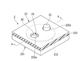
- FIG. 1 is an exploded perspective view showing a schematic configuration of the main wing 1.
- the main wing 1 includes a pair of spar 2 that forms both sides along the longitudinal direction, a pair of panels 3 that form an upper surface and a lower surface thereof, and a plurality of ribs 4 provided inside the spar.
- the pair of spar 2 includes a front spar 21 that forms a side portion on the front side of the aircraft among both side portions of the main wing 1, and a rear spar 22 that forms a side portion on the rear side of the aircraft. ing.
- the pair of spar 2 configured as described above is arranged at a predetermined interval so that the respective opening portions face each other.
- Both the front spar 21 and the rear spar 22 are members formed by molding carbon fiber reinforced plastic (CFRP).
- the pair of panels 3 includes an upper panel 31 that forms the upper surface of the main wing 1 and a lower panel 32 that forms the lower surface.
- the upper panel 31 includes a plate-shaped upper skin 31a having a curved cross-sectional shape, and a plurality of stringers 31b provided on one surface of the upper skin 31a to increase the bending rigidity.
- Both the upper skin 31a and the stringer 31b are members formed by molding carbon fiber reinforced plastic.
- the lower panel 32 has a lower skin 32a and a plurality of stringers 32b, both of which are members formed by molding carbon fiber reinforced plastic.
- the plurality of ribs 4 are members for structurally reinforcing the main wing 1. As shown in FIG. 1, the ribs 4 are provided at predetermined intervals in the longitudinal direction of the main wing 1. One end of each rib 4 is connected to the front spar 21 and the other end is connected to the rear spar 22. As a result, the front spar 21 and the rear spar 22 are held at regular intervals.
- the ribs 4 are all metal members.
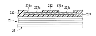
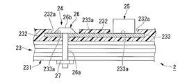
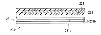
- FIG. 2 and 3 are views showing the spar 2 as the CFRP structure according to the first embodiment.
- FIG. 2 is a schematic perspective view showing a part of the spar 2
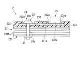
- FIG. 3 is a schematic cross-sectional view showing a cross section AA in FIG.
- the spar 2 includes a spar main body 23 made of CFRP, a jumper 24 provided through the spar main body 23, and an electronic device 25 attached to the surface of the spar main body 23.
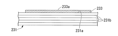
- the spar main body 23 includes a layered carbon fiber prepreg 231, a resin layer 232 formed on the surface 231 a of the carbon fiber prepreg 231, and a conductive layer embedded in the resin layer 232.
- Carbon fiber prepreg 231 serves as a reference potential point. As shown in FIG. 3, the carbon fiber prepreg 231 is formed by laminating a plurality of sheets 231b obtained by impregnating a carbon fiber with a thermosetting resin (not shown) and curing the thermosetting resin. Are integrated. And this carbon fiber prepreg 231 comprised with a carbon fiber has electroconductivity.
- the resin layer 232 is configured by forming on the surface 231a of the carbon fiber prepreg 231 a thermosetting resin that exudes from the carbon fiber when the thermosetting resin is cured.
- This resin layer 232 made of a thermosetting resin is an insulator having no conductivity. As shown in FIGS. 2 and 3, the resin layer 232 is formed so as to cover the surface 231a of the carbon fiber prepreg 231. The resin layer 232 penetrates the predetermined portion to expose the conductive layer 233. A plurality of holes 232a are formed.
- the conductive layer 233 is a thin plate member made of a metal such as copper or aluminum and has conductivity. As shown in FIGS. 2 and 3, the conductive layer 233 is formed in a substantially circular shape in plan view. The conductive layer 233 is formed thinner than the resin layer 232. The conductive layer 233 configured as described above is provided on the carbon fiber prepreg 231 in a state of being embedded in the resin layer 232. The material and shape of the conductive layer 233 are not limited to the present embodiment, and the design can be changed as appropriate.
- the jumper 24 electrically connects the conductive layer 233 and the carbon fiber prepreg 231. As shown in FIGS. 2 and 3, the jumper 24 includes a metal bolt 26 provided through the spar main body 23 and a nut 27 screwed into the bolt 26.
- the bolt 26 has a shaft portion 26a with a male screw (not shown) cut on the peripheral surface, and an umbrella-shaped head portion 26b provided at one end of the shaft portion 26a.
- the bolt 26 configured in this manner is disposed at the position of the conductive layer exposure hole 232 a formed in the resin layer 232.
- the shaft portion 26 a of the bolt 26 is inserted through the conductive layer 233 and the carbon fiber prepreg 231.
- the lower surface of the head portion 26b of the bolt 26 is in contact with the surface 233a of the conductive layer 233 exposed from the conductive layer exposure hole 232a.
- the tip end of the shaft portion 26a protrudes from the back surface of the spar main body 23, and a nut 27 is screwed to the protruding shaft portion 26a.
- the jumper 24 is fixed to the spar main body 23 by tightening the spar main body 23 in the thickness direction by the head 26 b of the bolt 26 and the nut 27.
- the electronic device 25 is installed at the position of the conductive layer exposure hole 232a formed in the resin layer 232, and with respect to the surface 233a of the conductive layer 233 exposed from the conductive layer exposure hole 232a. Its lower surface is in contact. Therefore, the electronic device 25 is electrically connected to the carbon fiber prepreg 231 through the conductive layer 233 that contacts the electronic device 25 and the jumper 24 that contacts the conductive layer 233. Thereby, the electronic device 25 is in a state in which conduction with the reference potential point is ensured.
- the shape, size, and the like of the electronic device 25 are not limited to the present embodiment, and can be appropriately changed in design.
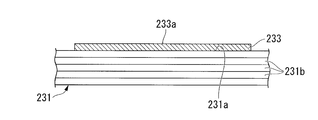
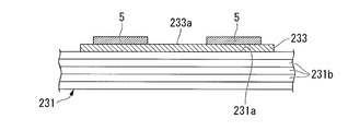
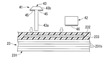
- 4A, 4B, 4C, 5A, and 5B are explanatory views showing manufacturing steps of the spar 2 according to the first embodiment.
- the worker forms the conductive layer 233 on the surface 231 a of the carbon fiber prepreg 231. That is, as shown in FIG. 4A, the operator stacks a plurality of carbon fiber sheets 231b soaked with a thermosetting resin. The worker arranges the conductive layer 233 at a predetermined position on the surface 231a of the carbon fiber prepreg 231 as shown in FIGS. 2 and 4A.
- the position where the conductive layer 233 is disposed on the surface 231a of the carbon fiber prepreg 231 is not limited to this embodiment, and can be arbitrarily changed according to the position where the electronic device 25 or the jumper 24 is to be installed.
- the worker masks the surface 231a of the conductive layer 233. That is, the operator removes the masking tape 5 cut according to the shape of the conductive layer exposure hole 232a shown in FIG. 2 at a predetermined position on the surface 231a of the conductive layer 233 as shown in FIG.
- the jumper 24 is affixed to each position where the jumper 24 is to be installed.
- the operator cures the carbon fiber prepreg 231. That is, an operator pressurizes and heats the carbon fiber prepreg 231 in a state where the conductive layer 233 is disposed on the surface 231a using a so-called autoclave. Then, the thermosetting resin soaked in each sheet 231b constituting the carbon fiber prepreg 231 is cured, so that each sheet 231b is integrated via the thermosetting resin. At this time, as shown in FIG. 4C, the resin layer 232 is formed by laminating the thermosetting resin exuded from each sheet 231 b so as to cover the surface 231 a of the carbon fiber prepreg 231. As a result, the conductive layer 233 is buried in the resin layer 232. The resin layer 232 is not formed at the position where the masking tape 5 is applied on the surface 233a of the conductive layer 233.
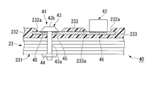
- the worker forms the conductive layer exposure hole 232a. That is, the operator removes the masking tape 5 from the state shown in FIG. 4C.
- the surface 233a of the conductive layer 233 below the masking tape 5 is removed as shown in FIG. 5A. Is exposed.
- a conductive layer exposure hole 232 a is formed in the resin layer 232.
- the operator causes the jumper 24 to penetrate the spar main body 23 thus formed. That is, as shown in FIG. 5B, the operator penetrates the shaft portion 26 a of the bolt 26 constituting the jumper 24 through the conductive layer 233 exposed from the conductive layer exposure hole 232 a of the resin layer 232. The operator penetrates the shaft portion 26a through the resin layer 232 below the conductive layer 233 and further into the carbon fiber prepreg 231 below. Then, the lower surface of the head 26 b of the bolt 26 is brought into contact with the surface 233 a of the conductive layer 233.
- the operator fixes the jumper 24 to the spar main body 23 by screwing and tightening the nut 27 to the shaft portion 26 a of the bolt 26 protruding from the back surface of the spar main body 23.
- the strength of the carbon fiber prepreg 231 is reduced if the carbon fiber is cut. Accordingly, the operator inserts the bolts 26 into the void portions of the mesh-like carbon fibers so as to prevent the carbon fibers from being cut by the bolts 26 while ensuring the contact between the bolts 26 and the carbon fibers, and pushes the meshes so that the bolts are spread. It is desirable to penetrate 26.
- the worker attaches the electronic device 25 to the spar main body 23. That is, as shown in FIG. 5B, the operator places the electronic device 25 on the surface 233a of the conductive layer 233 exposed from the conductive layer exposure hole 232a of the resin layer 232 so that the lower surface of the electronic device 25 contacts the surface 233a of the conductive layer 233. And attach. Accordingly, the electronic device 25 is electrically connected to the carbon fiber prepreg 231 serving as a reference potential point via the conductive layer 233 that is in contact with the electronic device 25 and the jumper 24 that is in contact with the conductive layer 233. Thereby, the electronic device 25 is in a state in which conduction with the reference potential point is ensured. Thus, the spar 2 as the CFRP structure is completed.
- the masking tape 5 locally forms the resin layer 232 on the surface 233a of the conductive layer 233 when the carbon fiber prepreg 231 is cured. Blocking. Therefore, the jumper 24 and the conductive layer 233 can be more reliably electrically connected.
- the electronic device 25 can be placed in direct contact with the conductive layer 233. Accordingly, it is not necessary to separately provide a wiring or the like for electrically connecting the electronic device 25 and the conductive layer 233, so that the electronic device 25 can be grounded with a simple configuration.
- the head portion 26b provided on the jumper 24 is brought into contact with the surface 233a of the conductive layer 233, the conductive layer 233 and the jumper 24 can be more reliably electrically connected by the head portion 26b.
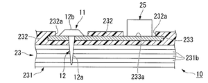
- FIG. 6 is a schematic cross-sectional view showing the configuration of the spar 10 according to the second embodiment.
- the spar 10 according to the second embodiment differs from the spar 2 according to the first embodiment shown in FIG. 3 only in the configuration of the jumper 11. Since other configurations are the same as those in the first embodiment, the same reference numerals as those in FIG. 3 are used, and description thereof is omitted here.
- the jumper 11 according to the second embodiment is composed of only metal bolts 12 provided through the spar main body 23.
- bolt 12 is the same as the volt
- the shape of the shaft portion 12a is different from the bolt 26 of the first embodiment. More specifically, the shaft portion 12a of the bolt 12 of the second embodiment has a wedge-shaped cross-sectional shape, that is, a cross-sectional shape in which the width gradually decreases from the proximal end side toward the distal end side along the longitudinal direction thereof. Yes.
- the tip of the shaft portion 12a of the bolt 12 is narrow. Therefore, in the process of allowing the operator to penetrate the shaft portion 12a through the spar body 23, the tip end of the shaft portion 12a is inserted while expanding the void portion of the net-like carbon fiber constituting the carbon fiber prepreg 231. Further, as the shaft portion 12a is inserted deeply into the carbon fiber prepreg 231, the shaft portion 12a that gradually becomes wider toward the base end side spreads the carbon fiber mesh. Therefore, the carbon fiber is not cut, the continuity of the carbon fiber as the conductor is ensured, and the electrical conductivity of the entire carbon fiber can be ensured.
- FIG. 7A, FIG. 7B, FIG. 7C, and FIG. 7D are explanatory views showing manufacturing steps of the spar 40 according to the third embodiment.
- the spar 40 according to the third embodiment differs from the spar 40 according to the first embodiment shown in FIG. 3 in the configurations of the jumper 41 and the electronic device 42. Since other configurations are the same as those in the first embodiment, the same reference numerals as those in FIG. 3 are used, and description thereof is omitted here.
- the jumper 41 includes a metal bolt 43 provided through the spar main body 23 and a nut 44 screwed into the bolt 43. is doing.
- bolt 43 is the same as the volt
- the bolt 43 is different from the bolt 43 of the first embodiment in that a plurality of protrusions 45 are provided on the lower surface of the head 43b.
- the protrusions 45 are each formed with a sharp tip.
- the electronic device 42 according to the third embodiment is different from the electronic device 42 of the first embodiment in that a plurality of protrusions 46 are provided on the lower surface thereof as shown in FIGS. 7C and 7D.
- the protrusions 46 are also each formed with a sharp tip.
- the mounting work to the spar main body 23 can be simplified by using the protrusions 45 and 46 provided on the lower surface thereof. More specifically, as shown in FIG. 7A, an operator who intends to manufacture the spar 40 according to the third embodiment first forms the conductive layer 233 on the surface 231a of the carbon fiber prepreg 231. That is, as in the first embodiment, the operator stacks a plurality of carbon fiber sheets 231b soaked with thermosetting resin, and disposes the conductive layer 233 at a predetermined position on the surface 231a of the carbon fiber prepreg 231.
- the operator pressurizes and heats the carbon fiber prepreg 231 to cure the thermosetting resin, thereby curing the carbon fiber prepreg 231.
- the resin layer 232 is formed by forming the thermosetting resin that has oozed from the sheet 231 b constituting each carbon fiber prepreg 231 on the surface 231 a of the carbon fiber prepreg 231.
- the resin layer 232 is formed over the entire surface 231a of the carbon fiber prepreg 231.
- the operator causes the jumper 41 to penetrate the spar main body 23. That is, as shown in FIG. 7C, the operator causes the shaft 43 a of the bolt 43 constituting the jumper 41 to penetrate the resin layer 232. Further, the shaft portion 43 a is penetrated from the conductive layer 233 below the resin layer 232 to the resin layer 232 below and finally to the carbon fiber prepreg 231. Then, as shown in FIG. 7D, the worker brings the lower surface of the head 43 b of the bolt 43 into contact with the surface 233 a of the conductive layer 233. At this time, the sharp protrusion 45 provided on the lower surface of the head 43 b breaks the resin layer 232.
- the lower surface of the head portion 43b of the bolt 43 can be reliably brought into contact with the surface 233a of the conductive layer 233, and conduction between the conductive layer 23 and the carbon fiber prepreg 231 can be ensured. Then, the operator fixes the jumper 41 to the spar main body 23 by screwing and tightening the nut 44 to the shaft portion 43 a of the bolt 43 protruding from the back surface of the spar main body 23.
- the worker attaches the electronic device 42 to the spar main body 23. That is, as shown in FIG. 7C, the worker attaches the electronic device 42 to the spar main body 23 such that the lower surface thereof is in contact with the surface 233 a of the conductive layer 233.
- the sharp protrusion 46 provided on the lower surface of the electronic device 42 breaks the resin layer 232, whereby the lower surface of the electronic device 42 can be reliably brought into contact with the surface 233 a of the conductive layer 233.
- the method for manufacturing the spar 40 according to the third embodiment it is not necessary to perform a pretreatment such as masking the surface 231a prior to the step of curing the carbon fiber prepreg 231. Labor saving by reducing the cost and cost reduction by reducing the masking tape 5 and the like can be achieved.
- the protrusion 45 and the protrusion 46 are provided on each of the jumper 41 and the electronic device 42.
- the provision of the protrusion 46 on the lower surface of the electronic device 42 is not essential to the present invention, and at least the jumper 41. It is sufficient if the protrusion 45 is provided on the surface.
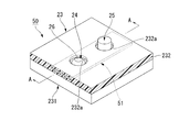
- FIG. 8 is a schematic perspective view showing a part of the spar 50 according to the fourth embodiment.
- the spar 50 according to the fourth embodiment differs from the spar 2 according to the first embodiment shown in FIG. 2 only in the configuration of the conductive layer 51. Since the other configuration is the same as that of the first embodiment, the same reference numerals as those in FIG.
- the conductive layer 51 according to the fourth embodiment is a metal thin plate member and has conductivity, is formed with a thickness smaller than that of the resin layer 232, and is embedded in the resin layer 232.
- the conductive layer 233 is the same as the conductive layer 233 of the first embodiment in that the conductive layer 233 is provided.
- the conductive layer 51 according to the fourth embodiment is different from the conductive layer 233 according to the first embodiment in that the conductive layer 51 is formed in a strip shape in a plan view, that is, in an elongated substantially rectangular shape.
- the dimension to the longitudinal direction of the conductive layer 51 is set substantially equal to the width dimension of the carbon fiber prepreg 231.
- both ends in the longitudinal direction of the conductive layer 51 reach both ends in the width direction of the carbon fiber prepreg 231. Therefore, although not shown in detail in the figure, when it is necessary to electrically connect the spar 50 shown in FIG. 8 and the spar 50 installed adjacent thereto, the longitudinal direction of the conductive layer 51 of each spar 50 If the ends are connected by electrical wiring, there is an advantage that the length of the electrical wiring can be minimized.
- the spar 2, 10, 40, 50 constituting the aircraft main wing 1 is described as an example of the CFRP structure.
- the CFRP structure is not limited to the spar 2, 10, 40, 50.
- the CFRP structure may be, for example, the upper surface skin 31a and the stringer 31b constituting the upper surface panel 31 shown in FIG. 1, the lower surface skin 32a and the stringer 32b constituting the lower surface panel 32, or the like.
- the CFRP structure is not limited to a component of the main wing 1 of an aircraft, and may be a component of an arbitrary structure.
- the present invention for example, is a structure that constitutes the main wing of an aircraft, and has a secondary function of grounding an electronic device attached to the surface of a carbon fiber reinforced plastic structure made of carbon fiber reinforced plastic. It can be applied to means for adding.
Landscapes
- Engineering & Computer Science (AREA)
- Mechanical Engineering (AREA)
- Aviation & Aerospace Engineering (AREA)
- Microelectronics & Electronic Packaging (AREA)
- Chemical & Material Sciences (AREA)
- Composite Materials (AREA)
- Manufacturing & Machinery (AREA)
- Moulding By Coating Moulds (AREA)
- Laminated Bodies (AREA)
- Reinforced Plastic Materials (AREA)
Priority Applications (6)
| Application Number | Priority Date | Filing Date | Title |
|---|---|---|---|
| CN201280008083.8A CN103347690B (zh) | 2011-02-16 | 2012-02-15 | 碳纤维强化塑料结构体及其制造方法 |
| CA2827396A CA2827396C (en) | 2011-02-16 | 2012-02-15 | Carbon-fiber-reinforced plastic structure and method for producing same |
| RU2013137704/05A RU2540649C1 (ru) | 2011-02-16 | 2012-02-15 | Конструкция из пластика, армированного углеволокном, и способ изготовления такой конструкции |
| BR112013020146A BR112013020146B1 (pt) | 2011-02-16 | 2012-02-15 | estrutura de plástico reforçada com fibra de carbono e métodos para produção da mesma |
| EP12747044.1A EP2676792B1 (en) | 2011-02-16 | 2012-02-15 | Carbon-fiber-reinforced plastic structure and method for producing same |
| US13/985,363 US10080286B2 (en) | 2011-02-16 | 2012-02-15 | Carbon-fiber-reinforced plastic structure and method for producing same |
Applications Claiming Priority (2)
| Application Number | Priority Date | Filing Date | Title |
|---|---|---|---|
| JP2011-030883 | 2011-02-16 | ||
| JP2011030883A JP5773679B2 (ja) | 2011-02-16 | 2011-02-16 | 炭素繊維強化プラスチック構造体及びその製造方法 |
Publications (1)
| Publication Number | Publication Date |
|---|---|
| WO2012111704A1 true WO2012111704A1 (ja) | 2012-08-23 |
Family
ID=46672617
Family Applications (1)
| Application Number | Title | Priority Date | Filing Date |
|---|---|---|---|
| PCT/JP2012/053522 WO2012111704A1 (ja) | 2011-02-16 | 2012-02-15 | 炭素繊維強化プラスチック構造体及びその製造方法 |
Country Status (8)
Cited By (3)
| Publication number | Priority date | Publication date | Assignee | Title |
|---|---|---|---|---|
| WO2014057960A1 (ja) * | 2012-10-09 | 2014-04-17 | 三菱重工業株式会社 | 構造体用構造材、燃料タンク、主翼及び航空機 |
| EP2979976A4 (en) * | 2013-03-26 | 2016-09-28 | Mitsubishi Heavy Ind Ltd | FUEL TANK, MAIN SURFACES, PLANE HULL, AIRPLANE AND MOBILE BODY |
| US10011366B2 (en) | 2012-03-26 | 2018-07-03 | Mitsubishi Heavy Industries, Ltd. | Fuel tank, main wing, aircraft fuselage, aircraft, and mobile body |
Families Citing this family (4)
| Publication number | Priority date | Publication date | Assignee | Title |
|---|---|---|---|---|
| JP5751871B2 (ja) | 2011-03-10 | 2015-07-22 | 三菱重工業株式会社 | 燃料タンク |
| JP6093192B2 (ja) * | 2013-01-25 | 2017-03-08 | 三菱航空機株式会社 | 航空機の機体用パネル、航空機の翼 |
| DE102015213271A1 (de) * | 2015-07-15 | 2017-01-19 | Siemens Aktiengesellschaft | Flugzeug mit einer Tragstruktur zur Übertragung elektrischer Energie zwischen einer Energiequelle und einem Energieverbraucher |
| CN119497357A (zh) * | 2023-08-14 | 2025-02-21 | 华为技术有限公司 | 一种结构件及电子设备 |
Citations (6)
| Publication number | Priority date | Publication date | Assignee | Title |
|---|---|---|---|---|
| JPH0263725A (ja) * | 1988-05-27 | 1990-03-05 | Mitsubishi Heavy Ind Ltd | 炭素繊維強化プラスチツク部材の組立方法 |
| JPH09193296A (ja) | 1996-01-11 | 1997-07-29 | Boeing Co:The | ハイブリッド積層、航空機の外板パネル、および胴体部分 |
| JP2007246967A (ja) * | 2006-03-15 | 2007-09-27 | Mitsubishi Heavy Ind Ltd | 成形体表面の導電化方法及び表面導電性成形体 |
| JP2009506952A (ja) * | 2005-09-06 | 2009-02-19 | ザ・ボーイング・カンパニー | 落雷保護用の銅グリッド修復技術 |
| JP2009227166A (ja) * | 2008-03-24 | 2009-10-08 | Mitsubishi Heavy Ind Ltd | 航空機組立品 |
| JP2010194749A (ja) * | 2009-02-23 | 2010-09-09 | Mitsubishi Heavy Ind Ltd | 樹脂基複合材の製造方法 |
Family Cites Families (15)
| Publication number | Priority date | Publication date | Assignee | Title |
|---|---|---|---|---|
| US3755713A (en) * | 1972-07-25 | 1973-08-28 | Boeing Co | Electrically conductive surface for aircraft |
| US3989984A (en) * | 1975-07-11 | 1976-11-02 | Mcdonnell Douglas Corporation | Aircraft lightning protection means |
| RU2041508C1 (ru) * | 1992-11-05 | 1995-08-09 | Московский авиационный технологический институт им.К.Э.Циолковского | Слоистый полимерный материал |
| US6327132B1 (en) * | 1998-06-10 | 2001-12-04 | Aerospatiale Matra | Spark resistant structure, in particular for aircraft |
| JP4119205B2 (ja) * | 2002-08-27 | 2008-07-16 | 富士通株式会社 | 多層配線基板 |
| US8231751B2 (en) * | 2005-09-06 | 2012-07-31 | The Boeing Company | Repair technique for lightning strike protection |
| DE102006031334A1 (de) | 2006-07-06 | 2008-01-10 | Airbus Deutschland Gmbh | Verfahren zur Herstellung eines Faserverbundbauteils für die Luft- und Raumfahrt |
| US7599164B2 (en) | 2006-12-07 | 2009-10-06 | The Boeing Company | Lightning protection system for aircraft composite structure |
| US7829796B2 (en) * | 2007-11-06 | 2010-11-09 | The Boeing Company | Circuit joining assembly materials for multi-layer lightning protection systems on composite aircraft |
| JP4719203B2 (ja) * | 2007-09-28 | 2011-07-06 | 三菱重工業株式会社 | 耐雷ファスナ |
| CA2739477C (en) | 2008-10-03 | 2016-12-20 | Short Brothers Plc | Fibre reinforced composite structures and method of manufacture |
| JP5769412B2 (ja) | 2010-12-17 | 2015-08-26 | 三菱重工業株式会社 | 構造物製造方法 |
| JP5730057B2 (ja) | 2011-02-16 | 2015-06-03 | 三菱重工業株式会社 | 炭素繊維強化プラスチック構造体 |
| JP5669635B2 (ja) * | 2011-03-14 | 2015-02-12 | 三菱航空機株式会社 | 機体構成部材の連結構造 |
| US9108363B2 (en) * | 2011-10-06 | 2015-08-18 | The Boeing Company | Thin wall bushing for robust electrical bonding to fiber-reinforced structures |
-
2011
- 2011-02-16 JP JP2011030883A patent/JP5773679B2/ja not_active Expired - Fee Related
-
2012
- 2012-02-15 RU RU2013137704/05A patent/RU2540649C1/ru active
- 2012-02-15 WO PCT/JP2012/053522 patent/WO2012111704A1/ja active Application Filing
- 2012-02-15 EP EP12747044.1A patent/EP2676792B1/en active Active
- 2012-02-15 CA CA2827396A patent/CA2827396C/en not_active Expired - Fee Related
- 2012-02-15 US US13/985,363 patent/US10080286B2/en active Active
- 2012-02-15 BR BR112013020146A patent/BR112013020146B1/pt not_active IP Right Cessation
- 2012-02-15 CN CN201280008083.8A patent/CN103347690B/zh not_active Expired - Fee Related
Patent Citations (6)
| Publication number | Priority date | Publication date | Assignee | Title |
|---|---|---|---|---|
| JPH0263725A (ja) * | 1988-05-27 | 1990-03-05 | Mitsubishi Heavy Ind Ltd | 炭素繊維強化プラスチツク部材の組立方法 |
| JPH09193296A (ja) | 1996-01-11 | 1997-07-29 | Boeing Co:The | ハイブリッド積層、航空機の外板パネル、および胴体部分 |
| JP2009506952A (ja) * | 2005-09-06 | 2009-02-19 | ザ・ボーイング・カンパニー | 落雷保護用の銅グリッド修復技術 |
| JP2007246967A (ja) * | 2006-03-15 | 2007-09-27 | Mitsubishi Heavy Ind Ltd | 成形体表面の導電化方法及び表面導電性成形体 |
| JP2009227166A (ja) * | 2008-03-24 | 2009-10-08 | Mitsubishi Heavy Ind Ltd | 航空機組立品 |
| JP2010194749A (ja) * | 2009-02-23 | 2010-09-09 | Mitsubishi Heavy Ind Ltd | 樹脂基複合材の製造方法 |
Non-Patent Citations (1)
| Title |
|---|
| See also references of EP2676792A4 |
Cited By (6)
| Publication number | Priority date | Publication date | Assignee | Title |
|---|---|---|---|---|
| US10011366B2 (en) | 2012-03-26 | 2018-07-03 | Mitsubishi Heavy Industries, Ltd. | Fuel tank, main wing, aircraft fuselage, aircraft, and mobile body |
| WO2014057960A1 (ja) * | 2012-10-09 | 2014-04-17 | 三菱重工業株式会社 | 構造体用構造材、燃料タンク、主翼及び航空機 |
| JP5852255B2 (ja) * | 2012-10-09 | 2016-02-03 | 三菱重工業株式会社 | 構造体用構造材、燃料タンク、主翼及び航空機 |
| US9776732B2 (en) | 2012-10-09 | 2017-10-03 | Mitsubishi Heavy Industries, Ltd. | Structural material for structure, fuel tank, main wing, and aircraft |
| EP2979976A4 (en) * | 2013-03-26 | 2016-09-28 | Mitsubishi Heavy Ind Ltd | FUEL TANK, MAIN SURFACES, PLANE HULL, AIRPLANE AND MOBILE BODY |
| US10046849B2 (en) | 2013-03-26 | 2018-08-14 | Mitsubishi Heavy Industries, Ltd. | Fuel tank, main wings, aircraft fuselage, aircraft, and moving body |
Also Published As
| Publication number | Publication date |
|---|---|
| CA2827396A1 (en) | 2012-08-23 |
| JP2012166506A (ja) | 2012-09-06 |
| BR112013020146A2 (pt) | 2016-11-08 |
| US10080286B2 (en) | 2018-09-18 |
| US20130319750A1 (en) | 2013-12-05 |
| BR112013020146B1 (pt) | 2020-04-07 |
| EP2676792A1 (en) | 2013-12-25 |
| RU2540649C1 (ru) | 2015-02-10 |
| EP2676792A4 (en) | 2017-11-22 |
| CA2827396C (en) | 2016-12-20 |
| JP5773679B2 (ja) | 2015-09-02 |
| CN103347690B (zh) | 2015-07-29 |
| CN103347690A (zh) | 2013-10-09 |
| EP2676792B1 (en) | 2019-05-01 |
Similar Documents
| Publication | Publication Date | Title |
|---|---|---|
| WO2012111704A1 (ja) | 炭素繊維強化プラスチック構造体及びその製造方法 | |
| US7599164B2 (en) | Lightning protection system for aircraft composite structure | |
| US20180156202A1 (en) | Spar cap assembly for a wind turbine rotor blade | |
| JP5237170B2 (ja) | 複合材タンク、翼、および、複合材タンクの製造方法 | |
| EP2930010B1 (de) | Gurtbaugruppe für ein Windenergieanlagenrotorblatt | |
| US7283095B2 (en) | Antenna assembly including z-pinning for electrical continuity | |
| WO2007030371A3 (en) | Copper grid repair technique for lightning strike protection | |
| AU2018260819B2 (en) | Lightning protection in aircrafts constructed with carbon fiber reinforced plastic | |
| JP4601428B2 (ja) | 複合航空機パネルの避雷および接地手段 | |
| JP6157749B2 (ja) | 繊維強化樹脂部材および繊維強化樹脂部材の製造方法 | |
| EP2561943B1 (en) | Drilling tool and method of drilling | |
| US9016615B2 (en) | Lightning and corrosion protection arrangement in an aircraft structural component | |
| EP2979976B1 (en) | Fuel tank, main wings, aircraft fuselage, aircraft, and moving body | |
| JP6770987B2 (ja) | 複合材構造体、航空機及び雷電流の誘導方法 | |
| US11801666B2 (en) | Structure formed from composite material |
Legal Events
| Date | Code | Title | Description |
|---|---|---|---|
| 121 | Ep: the epo has been informed by wipo that ep was designated in this application |
Ref document number: 12747044 Country of ref document: EP Kind code of ref document: A1 |
|
| ENP | Entry into the national phase |
Ref document number: 2827396 Country of ref document: CA |
|
| WWE | Wipo information: entry into national phase |
Ref document number: 13985363 Country of ref document: US Ref document number: 2012747044 Country of ref document: EP |
|
| NENP | Non-entry into the national phase |
Ref country code: DE |
|
| ENP | Entry into the national phase |
Ref document number: 2013137704 Country of ref document: RU Kind code of ref document: A |
|
| REG | Reference to national code |
Ref country code: BR Ref legal event code: B01A Ref document number: 112013020146 Country of ref document: BR |
|
| ENP | Entry into the national phase |
Ref document number: 112013020146 Country of ref document: BR Kind code of ref document: A2 Effective date: 20130807 |