WO2012111584A1 - 表示装置 - Google Patents
表示装置 Download PDFInfo
- Publication number
- WO2012111584A1 WO2012111584A1 PCT/JP2012/053217 JP2012053217W WO2012111584A1 WO 2012111584 A1 WO2012111584 A1 WO 2012111584A1 JP 2012053217 W JP2012053217 W JP 2012053217W WO 2012111584 A1 WO2012111584 A1 WO 2012111584A1
- Authority
- WO
- WIPO (PCT)
- Prior art keywords
- display device
- circuit board
- drive circuit
- display panel
- ground pattern
- Prior art date
- Legal status (The legal status is an assumption and is not a legal conclusion. Google has not performed a legal analysis and makes no representation as to the accuracy of the status listed.)
- Ceased
Links
Images



Classifications
-
- G—PHYSICS
- G02—OPTICS
- G02F—OPTICAL DEVICES OR ARRANGEMENTS FOR THE CONTROL OF LIGHT BY MODIFICATION OF THE OPTICAL PROPERTIES OF THE MEDIA OF THE ELEMENTS INVOLVED THEREIN; NON-LINEAR OPTICS; FREQUENCY-CHANGING OF LIGHT; OPTICAL LOGIC ELEMENTS; OPTICAL ANALOGUE/DIGITAL CONVERTERS
- G02F1/00—Devices or arrangements for the control of the intensity, colour, phase, polarisation or direction of light arriving from an independent light source, e.g. switching, gating or modulating; Non-linear optics
- G02F1/01—Devices or arrangements for the control of the intensity, colour, phase, polarisation or direction of light arriving from an independent light source, e.g. switching, gating or modulating; Non-linear optics for the control of the intensity, phase, polarisation or colour
- G02F1/13—Devices or arrangements for the control of the intensity, colour, phase, polarisation or direction of light arriving from an independent light source, e.g. switching, gating or modulating; Non-linear optics for the control of the intensity, phase, polarisation or colour based on liquid crystals, e.g. single liquid crystal display cells
- G02F1/133—Constructional arrangements; Operation of liquid crystal cells; Circuit arrangements
- G02F1/1333—Constructional arrangements; Manufacturing methods
- G02F1/133308—Support structures for LCD panels, e.g. frames or bezels
-
- G—PHYSICS
- G02—OPTICS
- G02F—OPTICAL DEVICES OR ARRANGEMENTS FOR THE CONTROL OF LIGHT BY MODIFICATION OF THE OPTICAL PROPERTIES OF THE MEDIA OF THE ELEMENTS INVOLVED THEREIN; NON-LINEAR OPTICS; FREQUENCY-CHANGING OF LIGHT; OPTICAL LOGIC ELEMENTS; OPTICAL ANALOGUE/DIGITAL CONVERTERS
- G02F1/00—Devices or arrangements for the control of the intensity, colour, phase, polarisation or direction of light arriving from an independent light source, e.g. switching, gating or modulating; Non-linear optics
- G02F1/01—Devices or arrangements for the control of the intensity, colour, phase, polarisation or direction of light arriving from an independent light source, e.g. switching, gating or modulating; Non-linear optics for the control of the intensity, phase, polarisation or colour
- G02F1/13—Devices or arrangements for the control of the intensity, colour, phase, polarisation or direction of light arriving from an independent light source, e.g. switching, gating or modulating; Non-linear optics for the control of the intensity, phase, polarisation or colour based on liquid crystals, e.g. single liquid crystal display cells
- G02F1/133—Constructional arrangements; Operation of liquid crystal cells; Circuit arrangements
- G02F1/1333—Constructional arrangements; Manufacturing methods
- G02F1/133308—Support structures for LCD panels, e.g. frames or bezels
- G02F1/133317—Intermediate frames, e.g. between backlight housing and front frame
-
- G—PHYSICS
- G02—OPTICS
- G02F—OPTICAL DEVICES OR ARRANGEMENTS FOR THE CONTROL OF LIGHT BY MODIFICATION OF THE OPTICAL PROPERTIES OF THE MEDIA OF THE ELEMENTS INVOLVED THEREIN; NON-LINEAR OPTICS; FREQUENCY-CHANGING OF LIGHT; OPTICAL LOGIC ELEMENTS; OPTICAL ANALOGUE/DIGITAL CONVERTERS
- G02F1/00—Devices or arrangements for the control of the intensity, colour, phase, polarisation or direction of light arriving from an independent light source, e.g. switching, gating or modulating; Non-linear optics
- G02F1/01—Devices or arrangements for the control of the intensity, colour, phase, polarisation or direction of light arriving from an independent light source, e.g. switching, gating or modulating; Non-linear optics for the control of the intensity, phase, polarisation or colour
- G02F1/13—Devices or arrangements for the control of the intensity, colour, phase, polarisation or direction of light arriving from an independent light source, e.g. switching, gating or modulating; Non-linear optics for the control of the intensity, phase, polarisation or colour based on liquid crystals, e.g. single liquid crystal display cells
- G02F1/133—Constructional arrangements; Operation of liquid crystal cells; Circuit arrangements
- G02F1/1333—Constructional arrangements; Manufacturing methods
- G02F1/133308—Support structures for LCD panels, e.g. frames or bezels
- G02F1/13332—Front frames
-
- G—PHYSICS
- G02—OPTICS
- G02F—OPTICAL DEVICES OR ARRANGEMENTS FOR THE CONTROL OF LIGHT BY MODIFICATION OF THE OPTICAL PROPERTIES OF THE MEDIA OF THE ELEMENTS INVOLVED THEREIN; NON-LINEAR OPTICS; FREQUENCY-CHANGING OF LIGHT; OPTICAL LOGIC ELEMENTS; OPTICAL ANALOGUE/DIGITAL CONVERTERS
- G02F1/00—Devices or arrangements for the control of the intensity, colour, phase, polarisation or direction of light arriving from an independent light source, e.g. switching, gating or modulating; Non-linear optics
- G02F1/01—Devices or arrangements for the control of the intensity, colour, phase, polarisation or direction of light arriving from an independent light source, e.g. switching, gating or modulating; Non-linear optics for the control of the intensity, phase, polarisation or colour
- G02F1/13—Devices or arrangements for the control of the intensity, colour, phase, polarisation or direction of light arriving from an independent light source, e.g. switching, gating or modulating; Non-linear optics for the control of the intensity, phase, polarisation or colour based on liquid crystals, e.g. single liquid crystal display cells
- G02F1/133—Constructional arrangements; Operation of liquid crystal cells; Circuit arrangements
- G02F1/1333—Constructional arrangements; Manufacturing methods
- G02F1/133308—Support structures for LCD panels, e.g. frames or bezels
- G02F1/133322—Mechanical guidance or alignment of LCD panel support components
-
- G—PHYSICS
- G02—OPTICS
- G02F—OPTICAL DEVICES OR ARRANGEMENTS FOR THE CONTROL OF LIGHT BY MODIFICATION OF THE OPTICAL PROPERTIES OF THE MEDIA OF THE ELEMENTS INVOLVED THEREIN; NON-LINEAR OPTICS; FREQUENCY-CHANGING OF LIGHT; OPTICAL LOGIC ELEMENTS; OPTICAL ANALOGUE/DIGITAL CONVERTERS
- G02F1/00—Devices or arrangements for the control of the intensity, colour, phase, polarisation or direction of light arriving from an independent light source, e.g. switching, gating or modulating; Non-linear optics
- G02F1/01—Devices or arrangements for the control of the intensity, colour, phase, polarisation or direction of light arriving from an independent light source, e.g. switching, gating or modulating; Non-linear optics for the control of the intensity, phase, polarisation or colour
- G02F1/13—Devices or arrangements for the control of the intensity, colour, phase, polarisation or direction of light arriving from an independent light source, e.g. switching, gating or modulating; Non-linear optics for the control of the intensity, phase, polarisation or colour based on liquid crystals, e.g. single liquid crystal display cells
- G02F1/133—Constructional arrangements; Operation of liquid crystal cells; Circuit arrangements
- G02F1/1333—Constructional arrangements; Manufacturing methods
- G02F1/133382—Heating or cooling of liquid crystal cells other than for activation, e.g. circuits or arrangements for temperature control, stabilisation or uniform distribution over the cell
-
- G—PHYSICS
- G02—OPTICS
- G02F—OPTICAL DEVICES OR ARRANGEMENTS FOR THE CONTROL OF LIGHT BY MODIFICATION OF THE OPTICAL PROPERTIES OF THE MEDIA OF THE ELEMENTS INVOLVED THEREIN; NON-LINEAR OPTICS; FREQUENCY-CHANGING OF LIGHT; OPTICAL LOGIC ELEMENTS; OPTICAL ANALOGUE/DIGITAL CONVERTERS
- G02F1/00—Devices or arrangements for the control of the intensity, colour, phase, polarisation or direction of light arriving from an independent light source, e.g. switching, gating or modulating; Non-linear optics
- G02F1/01—Devices or arrangements for the control of the intensity, colour, phase, polarisation or direction of light arriving from an independent light source, e.g. switching, gating or modulating; Non-linear optics for the control of the intensity, phase, polarisation or colour
- G02F1/13—Devices or arrangements for the control of the intensity, colour, phase, polarisation or direction of light arriving from an independent light source, e.g. switching, gating or modulating; Non-linear optics for the control of the intensity, phase, polarisation or colour based on liquid crystals, e.g. single liquid crystal display cells
- G02F1/133—Constructional arrangements; Operation of liquid crystal cells; Circuit arrangements
- G02F1/1333—Constructional arrangements; Manufacturing methods
- G02F1/1345—Conductors connecting electrodes to cell terminals
- G02F1/13452—Conductors connecting driver circuitry and terminals of panels
Definitions
- the present invention relates to a display device, and more particularly to a heat dissipation structure of a drive circuit mounted on a circuit board.
- an optical sheet that diffuses light toward a display panel that displays an image is disposed on the front surface of the backlight chassis that supports the light source, and a mounting body is disposed on the front side peripheral portion of the optical sheet.
- the optical sheet is attached to the backlight chassis by the attachment body.
- FIG. 7A is a cross section showing the structure of the display device 100 of Patent Document 1 as an example of a conventional display device.
- a panel support frame 109 is provided on the front edge portion of the optical sheet 107 via a spacer 108.
- a display panel 110 that displays an image is supported in front of the panel support frame 109.
- a bezel 112 is provided on the front edge of the display panel 110 via a flexible body 111.
- the panel support frame 109 is provided with a circuit board 115 for driving the display panel 110.
- JP 2009-294520 A (published on Dec. 17, 2009)
- FIG. 7B is an enlarged view of part A to which the circuit board 115 is attached.
- the circuit board 115 has a driving circuit 116 for driving the display panel 110 and is disposed inside the display device 100 which is sealed so that dust does not enter. For this reason, the heat generated from the drive circuit 116 is not directly radiated to the outside. For example, the heat is transmitted little by little from the panel support frame 109b to the backlight chassis 104c and diffused throughout the backlight chassis 104. It had been dissipated.
- an object of the present invention is to provide a display device that can sufficiently dissipate heat of a drive circuit disposed inside even in a sealed display device. It is to provide.
- a display device comprising: a display panel; a metal bezel that holds the peripheral edge of the display panel from the outside; a drive circuit that drives the display panel; and a circuit board on which the drive circuit is mounted.
- the metal bezel has a convex portion on the inner surface, and the convex portion is in contact with the ground pattern.
- the present invention it is possible to efficiently dissipate the heat of the drive circuit arranged inside the hermetic seal of the display device, and it is possible to prevent the temperature of the drive circuit from rising and the reliability from being lowered.
- FIG. 1 It is sectional drawing of the display apparatus which is the 1st Embodiment of this invention. It is a top view of a circuit board. It is a sectional view showing the installation location of the circuit board. It is a cross-sectional view of a second embodiment of the display device of the present invention. It is a figure of a circuit board. (A) shows a circuit board in plan view, and (b) is a cross section of the circuit board. It is a figure of a circuit board. (A) shows a circuit board in plan view, and (b) is a cross section of the circuit board. It is a cross-sectional view of a conventional display device. (A) is a cross section of a conventional display device, and (b) is an enlarged view of part A of (a).
- FIG. 1 is a cross-sectional view illustrating a schematic configuration of a display device 1 according to a first embodiment of the invention.
- the display device 1 includes a display panel 2, and a backlight unit 3 is disposed on the back side of the display panel 2.
- liquid crystal is filled between a pair of substrates including a TFT (thin film transistor) substrate 21 and a CF (color filter) substrate 22.
- the display panel 2 transmits light emitted from the backlight unit 3 and displays it as an image on the front side.
- the backlight unit 3 includes a shallow, substantially box-shaped metal chassis 4, in which a plurality of CCFLs (cold cathode fluorescent lamps) 5 serving as light sources and CCFL 5 light are displayed on a display panel. reflecting sheets 6 to be reflected on the 2 side is provided.
- An optical sheet 7 for adjusting light incident on the display panel 2 is installed on the front side of the metal chassis 4.
- the optical sheet 7 is laminated with optical members such as a diffusion plate, a diffusion sheet, a lens sheet, and a polarizing sheet.
- a frame-shaped resin frame 8 is attached to the front edge of the optical sheet 7, and the optical sheet 7 is sandwiched between the metal chassis 4 and the resin frame 8.
- a display panel 2 is installed on the front edge of the resin frame 8.
- a frame-shaped metal bezel 9 is attached to the front edge of the display panel 2, and the display panel 2 is sandwiched between the metal bezel 9 and the resin frame 8.
- the metal bezel 9 is formed in a quadrilateral frame shape opened from a metal plate material such as stainless steel by pressing or the like. Each side of the metal bezel 9 has an inverted L-shaped cross section having an upper wall 9a and a side wall 9b, and the side wall 9b stands up toward the back side.
- the metal bezel 9 is a member having a function of holding or protecting the peripheral edge of the display panel 2, and is attached so as to cover the front edge and the side of the display panel 2.
- a circuit board 10 for driving the display panel 2 is provided inside the metal bezel 9.
- the circuit board 10 is connected to a source wiring 23 and the like formed on the TFT substrate 21 by an SOF (System On Film) 11.
- SOF System On Film
- the circuit board 10 can be arranged with a small frame width of the display device 1 by arranging the circuit board 10 in parallel with the side wall portion of the metal bezel 9.
- FIG. 2 is a plan view showing a state in which the circuit board 10 and the SOF 11 are connected.
- the circuit board 10 uses a multilayer board 10a in which insulating layers and wiring layers (not shown) are stacked and the respective layers are connected by through holes.
- a drive circuit 20 is mounted at the center of the circuit board 10, and is connected to a power source, a ground, a data wiring, and the like by a wiring 12 formed on the circuit board 10.
- the wiring 12 is provided at the edge of the circuit board 10 and is provided with a signal terminal 13 for connecting the SOF 11 and a spare dummy terminal 14 provided in parallel with the signal terminal 13.
- the SOF 11 is connected to the signal terminal 13, and signal input / output between the drive circuit 20 and the TFT substrate 21 is performed.
- a ground pattern 15 formed of a metal film is provided on the surface of the circuit board 10 to prevent external noise from entering, and is connected to the ground potential. Further, the surface of the circuit board 10 is covered with a solder resist except for the connection portion, and prevents and protects the metal film such as the wiring 12 from being corroded.
- the ground pattern 15 of the circuit board 10 is formed on the inner surface of the metal bezel 9.
- a feature is that a convex portion 9c is provided.
- the inner surface of the metal bezel 9 is a surface facing the inside of the display device 1 among the surfaces of the metal bezel 9.
- the convex portion 9 c is a metal member, and is formed by pressing a metal plate integrally with the metal bezel 9 or attached to the metal bezel 9 as a separate body. When the projections 9 c come into contact with the ground pattern 15 of the circuit board 10, heat generated by the drive circuit 20 mounted on the circuit board 10 can be conducted to the metal bezel 9 to be radiated.
- the portion where the convex portion 9 c comes into contact is the peripheral portion of the drive circuit 20 indicated by broken lines 9 c and 9 d in FIG. 2. Therefore, the center of the convex portion 9c is a concave portion as shown by a broken line 9d so that the drive circuit 20 does not hit.
- the metal bezel 9 is fitted from the side surface side of the display device 1 with the recess 9 d corresponding to the drive circuit 20 of the circuit board 10, and the protrusion 9 c of the metal bezel 9 is attached in contact with the ground pattern 15. .
- the ground pattern 15 comes into contact with the convex portion 9c of the metal bezel 9 in the peripheral portion of the drive circuit 20, so that the heat generated in the drive circuit 20 is the ground pattern 15 that is a metal material having excellent thermal conductivity. Since the heat is transferred to the metal bezel 9 by transferring heat to the convex portion 9c, the heat generated by the drive circuit 20 can be efficiently radiated to the outside of the metal bezel 9. For this reason, it is possible to prevent the reliability of the drive circuit 20 from increasing due to temperature rise.
- the ground pattern 15 comes into contact with the convex portion 9c and is electrically connected to the metal bezel 9, so that the potential of the ground is strengthened and static electricity is hardly accumulated on the circuit board 10, and ESD (Electro-Static) it is possible to prevent destruction of the drive circuit 20 according Discharge).
- ESD Electro-Static
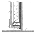
- FIG. 3 is a schematic cross-sectional view showing an optimal arrangement of the circuit board 10 in the display device 1.
- the structure of the upper part of the display device 1 shown in FIG. 1 and the lower part close to the leg 30 of the display device 1 shown in FIG. As indicated by the arrows, the heat generated from the CCFL 5 etc. rises inside the display device 1 and accumulates in the upper portion. Therefore, the temperature of the metal bezel 9 is lower in the lower portion than in the upper portion of the display device 1. It is low.
- the heat dissipation efficiency of the drive circuit 20 can be increased by disposing the circuit board 10 below the display device 1 and bringing it into contact with the portion of the metal bezel 9 where the temperature is relatively low.
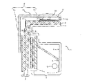
- FIG. 4 is a cross-sectional view illustrating a schematic configuration of the display device 1 according to the second embodiment of the invention.
- the display device 1 according to the second embodiment is configured such that the ground pattern 15 and the convex portion 9 c are in contact with each other at the edge portion of the circuit board 10. Therefore, the same reference numerals are added and detailed description is omitted.
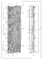
- FIG. 5 (a) is an enlarged view of the circuit board 10 shown in FIG. 4 in plan view
- FIG. 5 (b) is a cross section taken along line AA.
- the display device 1 according to the second embodiment extends a ground pattern 15 to a portion of a dummy terminal 14 that is arranged in parallel with the signal terminal 13 at the edge of the circuit board 10.
- the protrusion 9c of the metal bezel 9 is brought into contact with the ground pattern 15 provided.
- the ground pattern 15 and the protrusion can be reduced without reducing the effective mounting area on the circuit board 10. it can be brought into contact with 9c. For this reason, the heat generated by the drive circuit 20 and the SOF 11 can be transferred to the outside of the metal bezel 9 by transferring the heat to the ground pattern 15 and the projections 9c formed of a metal material having excellent thermal conductivity.
- the driving circuit 20 disposed at the center of the circuit board 10 is damaged by the protrusion 9c.
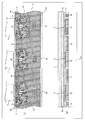
- FIG. 6 (a) shows another shape of the convex portion 9c in plan view
- FIG. 6 (b) is a cross section taken along the line AA.
- the convex portion 9 c shown in FIG. 6 is formed so as to contact the ground pattern 15 and also contact the upper portion of the SOF 11 connected on the signal terminal 13. Since the convex portion 9c abuts on the signal terminal 13 and the upper portion of the SOF 11, the SOF 11 is not separated from the signal terminal 13 to cause connection failure, and the reliability of the connection portion can be improved. Further, since the convex portion 9c can be formed by one piece and can be brought into contact with the plurality of ground patterns 15 at the same time, alignment and contact between the convex portions 9c and the ground pattern 15 can be easily performed. .
- the height is different at the positions of the ground pattern 15, the signal terminal 13, and the SOF 11, and a step is generated. Therefore, the height of the convex portion 9c is adjusted, or the convex portion 9c it is preferable to provide a conductive elastic member 17 to absorb the level difference.
- the convex portion may be in contact with the ground pattern provided around the drive circuit.
- the convex portion may be in contact with the ground pattern provided on the edge of the circuit board.
- the convex portion may be provided on a side wall portion of the metal bezel.
- the convex portion may be provided at a lower portion of the metal bezel.
Landscapes
- Physics & Mathematics (AREA)
- Nonlinear Science (AREA)
- Mathematical Physics (AREA)
- Chemical & Material Sciences (AREA)
- Crystallography & Structural Chemistry (AREA)
- General Physics & Mathematics (AREA)
- Optics & Photonics (AREA)
- Devices For Indicating Variable Information By Combining Individual Elements (AREA)
- Liquid Crystal (AREA)
Abstract
回路基板(10)に搭載された駆動回路(20)の温度上昇による信頼性低下を防止し、また、駆動回路(20)が静電気で破壊されることを防止した表示装置(1)を提供する。表示パネル(2)と、表示パネル(2)の周縁部を外側から保持する金属製ベゼル(9)と、表示パネル(2)を駆動する駆動回路(20)と、駆動回路(20)を搭載する回路基板(10)とを備えた表示装置(1)であって、回路基板(10)は、表面にグランドパターン(15)を有しており、金属製ベゼル(9)は、内面に凸部(9c)が設けられ、凸部(9c)は、グランドパターン(15)と接触されていることを特徴とする。
Description
本発明は表示装置に関するものであり、特に、回路基板に搭載された駆動回路の放熱構造に関するものである。
従来の表示装置は、光源を支持するバックライトシャーシの正面に、映像を表示する表示パネルに向けて光を拡散する光学シートを配置して、該光学シートの正面側周縁部分に取付体を配置し、該取付体により光学シートをバックライトシャーシに取り付けていた。
図7の(a)は、従来の表示装置の一例として、特許文献1の表示装置100の構造を示した断面である。表示装置100は、光学シート107の正面縁部に、スペーサ108を介して、パネル支持枠109が設けられている。パネル支持枠109の正面にて、映像表示する表示パネル110が支持されている。表示パネル110の正面縁部には可撓体111を介してベゼル112が設けられている。また、パネル支持枠109には、表示パネル110を駆動するための回路基板115が設けられている。
図7の(b)は、回路基板115が取り付けられているA部を拡大したものである。図7の(b)に示すように、回路基板115は、表示パネル110を駆動する駆動回路116を搭載し、塵埃が入り込まないように密閉された表示装置100の内部に配置されていた。このため、駆動回路116から発せられる熱は、外部に直接放熱されることがなく、例えば、パネル支持枠109bからバックライトシャーシ104cに少しずつ伝わり、バックライトシャーシ104の全体に拡散する等して放熱されていた。
しかしながら、近年、表示パネル110の大型化に伴い、回路基板115に実装される駆動回路116の発熱量が増加しており、図7の(b)に示す従来の構造では放熱が追いつかず、駆動回路116の温度が上昇し、信頼性が低下する問題があった。
そこで本発明は、上記課題を解決するためになされたものであり、その目的は、密閉された表示装置においても、内部に配置された駆動回路の熱を十分に放熱することができる表示装置を提供することにある。
表示パネルと、表示パネルの周縁部を外側から保持する金属製ベゼルと、表示パネルを駆動する駆動回路と、駆動回路を搭載する回路基板とを備えた表示装置であって、回路基板は、表面にグランドパターンを有しており、金属製ベゼルは、内面に凸部が設けられ、凸部は、グランドパターンと接触されていることを特徴とする。
本発明によれば、表示装置の密閉内部に配置された駆動回路の熱を効率よく放熱することができ、駆動回路の温度が上昇して、信頼性が低下することを防止できる。
以下、図面を参照して、本発明の実施の形態について説明する。
<実施例1>
図1は、本発明の実施例1に係る表示装置1の概略構成を示す断面図である。表示装置1は、表示パネル2を備え、表示パネル2の背面側にはバックライトユニット3が配置されている。表示パネル2は、TFT(薄膜トランジスタ)基板21とCF(カラーフィルタ)基板22とからなる一対の基板間に液晶が充填されている。この表示パネル2は、バックライトユニット3から照射される光を透過して、正面側に画像として表示する。
図1は、本発明の実施例1に係る表示装置1の概略構成を示す断面図である。表示装置1は、表示パネル2を備え、表示パネル2の背面側にはバックライトユニット3が配置されている。表示パネル2は、TFT(薄膜トランジスタ)基板21とCF(カラーフィルタ)基板22とからなる一対の基板間に液晶が充填されている。この表示パネル2は、バックライトユニット3から照射される光を透過して、正面側に画像として表示する。
バックライトユニット3は、浅底の略箱形状の金属製シャーシ4を備えており、その内部には、光源となる複数本のCCFL(冷陰極型蛍光ランプ)5と、CCFL5の光を表示パネル2側に反射させる反射シート6が備えられている。金属製シャーシ4の正面側には、表示パネル2に入射する光を調整する光学シート7が設置されている。光学シート7は、拡散板、拡散シート、レンズシート、偏光シートなどの光学部材が積層されている。
光学シート7の正面縁部には、枠状の樹脂製フレーム8が被着され、金属製シャーシ4と樹脂製フレーム8とにより光学シート7が挟持されている。また、樹脂製フレーム8の正面縁部には表示パネル2が設置されている。表示パネル2の正面縁部には枠状の金属製ベゼル9が被着され、金属製ベゼル9と樹脂製フレーム8とにより表示パネル2が挟持されている。
金属製ベゼル9は、ステンレス等の金属製の板材からプレス加工等により開口した四辺形の枠形状に形成されている。金属製ベゼル9の各辺は、上壁9aと側壁9bを有した断面が逆L字状の形状を有しており、側壁9bは背面側に向って起立している。この金属製ベゼル9は、表示パネル2の周縁部を保持する機能や保護する機能を有する部材であり、表示パネル2の正面縁部および側面部を覆うように被着されている。
また、金属製ベゼル9の内側には、表示パネル2を駆動する回路基板10が備えられている。この回路基板10は、SOF(System On Film)11でTFT基板21に形成されたソース配線23等と接続されている。図1に示すように、回路基板10は、金属製ベゼル9の側壁部と平行に配置することにより、表示装置1の額縁幅を小さくして配置することができる。
図2は、回路基板10とSOF11が接続された状態を示す平面図である。回路基板10には、図示しない絶縁層や配線層が積層され、各層間がスルーホールで接続された多層基板10aが用いられている。回路基板10の中央部には、駆動回路20が搭載されており、回路基板10に形成された配線12により、電源やグランド、データ配線等と接続されている。また、配線12は、回路基板10の縁部に延設され、SOF11を接続するための信号端子13や、信号端子13と一緒に並設された予備のダミー端子14が設けられている。信号端子13にはSOF11が接続されて、駆動回路20とTFT基板21との信号の入出力が行なわれる。
また、回路基板10の表面には、外部からのノイズの混入を防ぐために、金属膜で形成されたグランドパターン15が設けられ、グランドの電位に接続されている。さらに、回路基板10の表面は、接続部を除いてソルダーレジストに覆われ、配線12などの金属膜の腐食を防止し保護している。
本発明の実施例1は、金属製ベゼル9の内面に、回路基板10のグランドパターン15
に対応して、凸部9cが設けられていることを特徴としている。ここで、金属製ベゼル9の内面とは、金属製ベゼル9の有する面のうち、表示装置1の内側に面する面である。凸部9cは、金属製の部材であり、金属製ベゼル9と一体に金属製の板材をプレス加工して形成したり、別体として金属製ベゼル9に取り付けられる。この凸部9cが回路基板10のグランドパターン15と接触することにより、回路基板10に搭載された駆動回路20の発熱を金属製ベゼル9に熱伝導させて放熱することができる。
に対応して、凸部9cが設けられていることを特徴としている。ここで、金属製ベゼル9の内面とは、金属製ベゼル9の有する面のうち、表示装置1の内側に面する面である。凸部9cは、金属製の部材であり、金属製ベゼル9と一体に金属製の板材をプレス加工して形成したり、別体として金属製ベゼル9に取り付けられる。この凸部9cが回路基板10のグランドパターン15と接触することにより、回路基板10に搭載された駆動回路20の発熱を金属製ベゼル9に熱伝導させて放熱することができる。
グランドパターン15において、凸部9cが接触する部分は、図2の破線9cと9dで示す、駆動回路20の周辺部分である。したがって、凸部9cの中央は、駆動回路20が当たらないように、破線9dのように凹部になっている。
金属製ベゼル9は、凹部9dを回路基板10の駆動回路20に対応させながら、表示装置1の側面側から嵌め込まれて、金属製ベゼル9の凸部9cがグランドパターン15と接触して取り付けられる。
このように、駆動回路20の周辺部において、グランドパターン15が金属製ベゼル9の凸部9cと接触することにより、駆動回路20の発熱は、熱伝導性の優れた金属材料であるグランドパターン15と凸部9cを伝熱して、金属製ベゼル9に熱伝導されるので、駆動回路20の発熱を効率よく金属製ベゼル9の外側に放熱することができる。このため、駆動回路20が温度上昇して信頼性が低下することを防止できる。
また、グランドパターン15が凸部9cと接触して、金属製ベゼル9と電気的に導通することにより、グランドの電位が強化され、回路基板10に静電気が蓄積され難くなり、ESD(Electro-Static Discharge)による駆動回路20の破壊を防止することができる。
図3は、表示装置1において回路基板10の最適な配置を示す断面模式図である。図1に示した表示装置1の上部の構造と、図3に示す、表示装置1の脚部30に近い下部は、同様の構造となっている。そして、矢印で示すように、CCFL5等から発する熱は、表示装置1の内部を上昇して上部に蓄積されるため、金属製ベゼル9の温度は、表示装置1の上部よりも下部の方が低くなっている。
このため、回路基板10を表示装置1の下部に配置し、金属製ベゼル9の温度が比較的低い部分に接触させることより、駆動回路20の放熱効率を高めることができる。
<実施例2>
図4は、本発明の実施例2に係る表示装置1の概略構成を示す断面図である。図4に示すように、実施例2の表示装置1は、回路基板10の縁部でグランドパターン15と凸部9cが接触するように構成されており、他の構成は実施例1と同じであるため、同じ符号を付記して詳細な説明は省略する。
図4は、本発明の実施例2に係る表示装置1の概略構成を示す断面図である。図4に示すように、実施例2の表示装置1は、回路基板10の縁部でグランドパターン15と凸部9cが接触するように構成されており、他の構成は実施例1と同じであるため、同じ符号を付記して詳細な説明は省略する。
図5の(a)は、図4に示した回路基板10を平面視において拡大したものであり、図5の(b)は、A-A部の断面である。図5に示すように、実施例2の表示装置1は、回路基板10の縁部で信号端子13と一緒に並設されていたダミー端子14の個所に、グランドパターン15を延設し、延設したグランドパターン15に金属製ベゼル9の凸部9cを接触させている。
接続端子として通常使用されない予備のダミー端子14の部分を、金属製ベゼル9の凸部9cの接触部として用いることにより、回路基板10上の有効実装面積を減らすことなく、グランドパターン15と凸部9cを接触させることができる。このため、駆動回路20及びSOF11の発熱を、熱伝導性の優れた金属材料で形成されたグランドパターン15と凸部9cを伝熱させて、金属製ベゼル9の外側に放熱することができる。
また、グランドパターン15が回路基板10の縁部に延設され、その縁部に凸部9cを合わせるため、回路基板10の中央部に配置される駆動回路20は、凸部9cが当たって損壊する虞がなくなり、また、凸部9cの中央部には駆動回路20を避ける凹部9dを設けなくて済み、凸部9cを容易に形成することができる。
図6の(a)は、平面視において、凸部9cの別の形状を示し、図6の(b)は、A-A部における断面である。図6に示す凸部9cは、グランドパターン15と接触するとともに、信号端子13上に接続されるSOF11の上部にも当接するように形成されている。凸部9cが信号端子13とSOF11の上部に当接することにより、SOF11が信号端子13から離れて接続不良が生じることがなくなり、接続部の信頼性を向上させることができる。また、凸部9cは1個の形成で済ませることができ、複数のグランドパターン15と同時に接触させることができるので、凸部9cとグランドパターン15との位置合わせと接触を容易に行なうことができる。
なお、図6の(b)に示すように、グランドパターン15と信号端子13及びSOF11の位置では高さが異なり、段差が生じるため、凸部9cの高さを調整するか、凸部9cに段差を吸収する導電性の弾性部材17を設けることが好ましい。
また、本発明の表示装置は、前記凸部は、前記駆動回路の周囲に設けられた前記グランドパターンと接触されていてもよい。
前記凸部は、前記回路基板の縁部に設けられた前記グランドパターンと接触されていてもよい。
前記凸部は、前記金属製ベゼルの側壁部に設けられていてもよい。
前記凸部は、前記金属製ベゼルの下部に設けられていてもよい。
以上、本発明の実施形態について説明したが、本発明はこうした実施形態に何ら限定されるものではなく、本発明の要旨を逸脱しない範囲において、種々なる態様で実施できることは勿論である。
1 表示装置
2 表示パネル
3 バックライトユニット
4 金属製シャーシ
5 CCFL
6 反射シート
7 光学シート
8 樹脂製フレーム
9 金属製ベゼル
9a 上壁
9b 側壁
9c 凸部
9d 凹部
10 回路基板
10a 多層基板
11 SOF
12 配線
13 信号端子
14 ダミー端子
15 グランドパターン
17 導電性の弾性部材
20 駆動回路
21 TFT基板
22 CF基板
23 ソース配線
30 脚部
2 表示パネル
3 バックライトユニット
4 金属製シャーシ
5 CCFL
6 反射シート
7 光学シート
8 樹脂製フレーム
9 金属製ベゼル
9a 上壁
9b 側壁
9c 凸部
9d 凹部
10 回路基板
10a 多層基板
11 SOF
12 配線
13 信号端子
14 ダミー端子
15 グランドパターン
17 導電性の弾性部材
20 駆動回路
21 TFT基板
22 CF基板
23 ソース配線
30 脚部
Claims (5)
- 表示パネルと、
前記表示パネルの周縁部を外側から保持する金属製ベゼルと、
前記表示パネルを駆動する駆動回路と、
前記駆動回路を搭載する回路基板とを備えた表示装置であって、
前記回路基板は、表面にグランドパターンを有しており、
前記金属製ベゼルは、内面に凸部が設けられ、
前記凸部は、前記グランドパターンと接触されていることを特徴とする表示装置。 - 前記凸部は、前記駆動回路の周囲に設けられた前記グランドパターンと接触されていることを特徴とする請求項1に記載の表示装置。
- 前記凸部は、前記回路基板の縁部に設けられた前記グランドパターンと接触されていることを特徴とする請求項1に記載の表示装置。
- 前記凸部は、前記金属製ベゼルの側壁部に設けられていることを特徴とする請求項1乃至請求項3のいずれか1項に記載の表示装置。
- 前記凸部は、前記金属製ベゼルの下部に設けられていることを特徴とする請求項1乃至請求項4のいずれか1項に記載の表示装置。
Applications Claiming Priority (2)
| Application Number | Priority Date | Filing Date | Title |
|---|---|---|---|
| JP2011031820A JP2014081394A (ja) | 2011-02-17 | 2011-02-17 | 表示装置 |
| JP2011-031820 | 2011-02-17 |
Publications (1)
| Publication Number | Publication Date |
|---|---|
| WO2012111584A1 true WO2012111584A1 (ja) | 2012-08-23 |
Family
ID=46672503
Family Applications (1)
| Application Number | Title | Priority Date | Filing Date |
|---|---|---|---|
| PCT/JP2012/053217 Ceased WO2012111584A1 (ja) | 2011-02-17 | 2012-02-13 | 表示装置 |
Country Status (2)
| Country | Link |
|---|---|
| JP (1) | JP2014081394A (ja) |
| WO (1) | WO2012111584A1 (ja) |
Cited By (3)
| Publication number | Priority date | Publication date | Assignee | Title |
|---|---|---|---|---|
| JP2014175603A (ja) * | 2013-03-12 | 2014-09-22 | Mitsubishi Chemicals Corp | 面発光モジュール |
| WO2014187006A1 (zh) * | 2013-05-24 | 2014-11-27 | 深圳市华星光电技术有限公司 | 一种显示模组及显示器 |
| US20190384116A1 (en) * | 2016-07-13 | 2019-12-19 | Panasonic Liquid Crystal Display Co., Ltd. | Display device |
Families Citing this family (4)
| Publication number | Priority date | Publication date | Assignee | Title |
|---|---|---|---|---|
| JP2016021061A (ja) * | 2014-06-18 | 2016-02-04 | シャープ株式会社 | フレーム、表示装置、及びテレビジョン受像機 |
| JP6584143B2 (ja) * | 2015-05-27 | 2019-10-02 | 三菱電機株式会社 | バックライトおよび表示装置 |
| KR102351509B1 (ko) * | 2015-09-18 | 2022-01-13 | 엘지디스플레이 주식회사 | 디스플레이 장치 |
| JP6951687B2 (ja) * | 2018-03-19 | 2021-10-20 | 株式会社リコー | 画像投写装置及び移動体 |
Citations (3)
| Publication number | Priority date | Publication date | Assignee | Title |
|---|---|---|---|---|
| JPH06265922A (ja) * | 1993-03-12 | 1994-09-22 | Hitachi Ltd | 液晶表示装置 |
| JPH06347761A (ja) * | 1993-06-03 | 1994-12-22 | Hitachi Ltd | 液晶表示装置 |
| JPH09138389A (ja) * | 1995-11-16 | 1997-05-27 | Hitachi Ltd | 液晶表示装置 |
-
2011
- 2011-02-17 JP JP2011031820A patent/JP2014081394A/ja not_active Withdrawn
-
2012
- 2012-02-13 WO PCT/JP2012/053217 patent/WO2012111584A1/ja not_active Ceased
Patent Citations (3)
| Publication number | Priority date | Publication date | Assignee | Title |
|---|---|---|---|---|
| JPH06265922A (ja) * | 1993-03-12 | 1994-09-22 | Hitachi Ltd | 液晶表示装置 |
| JPH06347761A (ja) * | 1993-06-03 | 1994-12-22 | Hitachi Ltd | 液晶表示装置 |
| JPH09138389A (ja) * | 1995-11-16 | 1997-05-27 | Hitachi Ltd | 液晶表示装置 |
Cited By (4)
| Publication number | Priority date | Publication date | Assignee | Title |
|---|---|---|---|---|
| JP2014175603A (ja) * | 2013-03-12 | 2014-09-22 | Mitsubishi Chemicals Corp | 面発光モジュール |
| WO2014187006A1 (zh) * | 2013-05-24 | 2014-11-27 | 深圳市华星光电技术有限公司 | 一种显示模组及显示器 |
| US20190384116A1 (en) * | 2016-07-13 | 2019-12-19 | Panasonic Liquid Crystal Display Co., Ltd. | Display device |
| US11036086B2 (en) * | 2016-07-13 | 2021-06-15 | Panasonic Liquid Crystal Display Co., Ltd. | Display device |
Also Published As
| Publication number | Publication date |
|---|---|
| JP2014081394A (ja) | 2014-05-08 |
Similar Documents
| Publication | Publication Date | Title |
|---|---|---|
| US8405963B2 (en) | Display and damping member attached to display | |
| US7440046B2 (en) | Backlight assembly and liquid crystal display having the same | |
| WO2012111584A1 (ja) | 表示装置 | |
| JP2008026866A (ja) | 表示装置 | |
| WO2015059965A1 (ja) | 表示装置、及びテレビ受信装置 | |
| US20100039603A1 (en) | Display panel module | |
| CN110908180A (zh) | 照明装置、显示装置及照明装置的制造方法 | |
| TWI485482B (zh) | 具面板支撐結構之顯示模組 | |
| JP2015072794A (ja) | 液晶表示装置 | |
| KR100855812B1 (ko) | 액정 표시 장치 및 액정 표시 장치의 방진 방법 | |
| KR20110056966A (ko) | 방열이 용이한 액정표시소자 | |
| TWI643002B (zh) | 液晶顯示裝置 | |
| KR101937743B1 (ko) | 백라이트 유닛 및 이를 구비한 액정표시장치 | |
| KR20120072958A (ko) | 백라이트 및 이를 포함하는 액정표시소자 | |
| KR20100050136A (ko) | 액정표시장치 | |
| JP2010276934A (ja) | 液晶表示装置 | |
| KR102047223B1 (ko) | 엘이디를 사용하는 백라이트유닛 및 이를 포함하는 액정표시장치 | |
| JP5618162B2 (ja) | 液晶パネルモジュール及び液晶表示装置 | |
| KR101762694B1 (ko) | 장착부재를 포함하는 액정표시장치모듈 | |
| KR101279175B1 (ko) | 액정표시모듈 및 이를 갖는 액정표시장치 | |
| KR20070005806A (ko) | 백라이트 어셈블리 및 이를 이용한 액정표시장치 | |
| KR101361965B1 (ko) | 백라이트 유닛 및 이의 제조 방법과 이를 구비한 액정표시장치 | |
| JP5720973B2 (ja) | 液晶表示装置 | |
| KR20110127549A (ko) | 백라이트 유닛 | |
| KR20120009996A (ko) | 평판 표시장치 및 그 조립방법 |
Legal Events
| Date | Code | Title | Description |
|---|---|---|---|
| 121 | Ep: the epo has been informed by wipo that ep was designated in this application |
Ref document number: 12746543 Country of ref document: EP Kind code of ref document: A1 |
|
| NENP | Non-entry into the national phase |
Ref country code: DE |
|
| 122 | Ep: pct application non-entry in european phase |
Ref document number: 12746543 Country of ref document: EP Kind code of ref document: A1 |
|
| NENP | Non-entry into the national phase |
Ref country code: JP |