WO2012111462A1 - Organic electroluminescence element and illumination device - Google Patents
Organic electroluminescence element and illumination device Download PDFInfo
- Publication number
- WO2012111462A1 WO2012111462A1 PCT/JP2012/052584 JP2012052584W WO2012111462A1 WO 2012111462 A1 WO2012111462 A1 WO 2012111462A1 JP 2012052584 W JP2012052584 W JP 2012052584W WO 2012111462 A1 WO2012111462 A1 WO 2012111462A1
- Authority
- WO
- WIPO (PCT)
- Prior art keywords
- group
- ring
- layer
- organic
- general formula
- Prior art date
Links
Images


Classifications
-
- C—CHEMISTRY; METALLURGY
- C07—ORGANIC CHEMISTRY
- C07D—HETEROCYCLIC COMPOUNDS
- C07D213/00—Heterocyclic compounds containing six-membered rings, not condensed with other rings, with one nitrogen atom as the only ring hetero atom and three or more double bonds between ring members or between ring members and non-ring members
- C07D213/02—Heterocyclic compounds containing six-membered rings, not condensed with other rings, with one nitrogen atom as the only ring hetero atom and three or more double bonds between ring members or between ring members and non-ring members having three double bonds between ring members or between ring members and non-ring members
- C07D213/04—Heterocyclic compounds containing six-membered rings, not condensed with other rings, with one nitrogen atom as the only ring hetero atom and three or more double bonds between ring members or between ring members and non-ring members having three double bonds between ring members or between ring members and non-ring members having no bond between the ring nitrogen atom and a non-ring member or having only hydrogen or carbon atoms directly attached to the ring nitrogen atom
- C07D213/60—Heterocyclic compounds containing six-membered rings, not condensed with other rings, with one nitrogen atom as the only ring hetero atom and three or more double bonds between ring members or between ring members and non-ring members having three double bonds between ring members or between ring members and non-ring members having no bond between the ring nitrogen atom and a non-ring member or having only hydrogen or carbon atoms directly attached to the ring nitrogen atom with hetero atoms or with carbon atoms having three bonds to hetero atoms with at the most one bond to halogen, e.g. ester or nitrile radicals, directly attached to ring carbon atoms
- C07D213/78—Carbon atoms having three bonds to hetero atoms, with at the most one bond to halogen, e.g. ester or nitrile radicals
- C07D213/79—Acids; Esters
-
- H—ELECTRICITY
- H10—SEMICONDUCTOR DEVICES; ELECTRIC SOLID-STATE DEVICES NOT OTHERWISE PROVIDED FOR
- H10K—ORGANIC ELECTRIC SOLID-STATE DEVICES
- H10K50/00—Organic light-emitting devices
- H10K50/80—Constructional details
- H10K50/84—Passivation; Containers; Encapsulations
- H10K50/844—Encapsulations
-
- C—CHEMISTRY; METALLURGY
- C07—ORGANIC CHEMISTRY
- C07D—HETEROCYCLIC COMPOUNDS
- C07D221/00—Heterocyclic compounds containing six-membered rings having one nitrogen atom as the only ring hetero atom, not provided for by groups C07D211/00 - C07D219/00
- C07D221/02—Heterocyclic compounds containing six-membered rings having one nitrogen atom as the only ring hetero atom, not provided for by groups C07D211/00 - C07D219/00 condensed with carbocyclic rings or ring systems
- C07D221/04—Ortho- or peri-condensed ring systems
- C07D221/06—Ring systems of three rings
- C07D221/10—Aza-phenanthrenes
-
- C—CHEMISTRY; METALLURGY
- C07—ORGANIC CHEMISTRY
- C07D—HETEROCYCLIC COMPOUNDS
- C07D233/00—Heterocyclic compounds containing 1,3-diazole or hydrogenated 1,3-diazole rings, not condensed with other rings
- C07D233/54—Heterocyclic compounds containing 1,3-diazole or hydrogenated 1,3-diazole rings, not condensed with other rings having two double bonds between ring members or between ring members and non-ring members
- C07D233/56—Heterocyclic compounds containing 1,3-diazole or hydrogenated 1,3-diazole rings, not condensed with other rings having two double bonds between ring members or between ring members and non-ring members with only hydrogen atoms or radicals containing only hydrogen and carbon atoms, attached to ring carbon atoms
- C07D233/58—Heterocyclic compounds containing 1,3-diazole or hydrogenated 1,3-diazole rings, not condensed with other rings having two double bonds between ring members or between ring members and non-ring members with only hydrogen atoms or radicals containing only hydrogen and carbon atoms, attached to ring carbon atoms with only hydrogen atoms or radicals containing only hydrogen and carbon atoms, attached to ring nitrogen atoms
-
- C—CHEMISTRY; METALLURGY
- C07—ORGANIC CHEMISTRY
- C07D—HETEROCYCLIC COMPOUNDS
- C07D401/00—Heterocyclic compounds containing two or more hetero rings, having nitrogen atoms as the only ring hetero atoms, at least one ring being a six-membered ring with only one nitrogen atom
- C07D401/14—Heterocyclic compounds containing two or more hetero rings, having nitrogen atoms as the only ring hetero atoms, at least one ring being a six-membered ring with only one nitrogen atom containing three or more hetero rings
-
- C—CHEMISTRY; METALLURGY
- C07—ORGANIC CHEMISTRY
- C07D—HETEROCYCLIC COMPOUNDS
- C07D405/00—Heterocyclic compounds containing both one or more hetero rings having oxygen atoms as the only ring hetero atoms, and one or more rings having nitrogen as the only ring hetero atom
- C07D405/14—Heterocyclic compounds containing both one or more hetero rings having oxygen atoms as the only ring hetero atoms, and one or more rings having nitrogen as the only ring hetero atom containing three or more hetero rings
-
- C—CHEMISTRY; METALLURGY
- C07—ORGANIC CHEMISTRY
- C07D—HETEROCYCLIC COMPOUNDS
- C07D409/00—Heterocyclic compounds containing two or more hetero rings, at least one ring having sulfur atoms as the only ring hetero atoms
- C07D409/14—Heterocyclic compounds containing two or more hetero rings, at least one ring having sulfur atoms as the only ring hetero atoms containing three or more hetero rings
-
- C—CHEMISTRY; METALLURGY
- C07—ORGANIC CHEMISTRY
- C07D—HETEROCYCLIC COMPOUNDS
- C07D417/00—Heterocyclic compounds containing two or more hetero rings, at least one ring having nitrogen and sulfur atoms as the only ring hetero atoms, not provided for by group C07D415/00
- C07D417/14—Heterocyclic compounds containing two or more hetero rings, at least one ring having nitrogen and sulfur atoms as the only ring hetero atoms, not provided for by group C07D415/00 containing three or more hetero rings
-
- C—CHEMISTRY; METALLURGY
- C07—ORGANIC CHEMISTRY
- C07D—HETEROCYCLIC COMPOUNDS
- C07D471/00—Heterocyclic compounds containing nitrogen atoms as the only ring hetero atoms in the condensed system, at least one ring being a six-membered ring with one nitrogen atom, not provided for by groups C07D451/00 - C07D463/00
- C07D471/02—Heterocyclic compounds containing nitrogen atoms as the only ring hetero atoms in the condensed system, at least one ring being a six-membered ring with one nitrogen atom, not provided for by groups C07D451/00 - C07D463/00 in which the condensed system contains two hetero rings
- C07D471/04—Ortho-condensed systems
-
- C—CHEMISTRY; METALLURGY
- C07—ORGANIC CHEMISTRY
- C07D—HETEROCYCLIC COMPOUNDS
- C07D519/00—Heterocyclic compounds containing more than one system of two or more relevant hetero rings condensed among themselves or condensed with a common carbocyclic ring system not provided for in groups C07D453/00 or C07D455/00
-
- C—CHEMISTRY; METALLURGY
- C09—DYES; PAINTS; POLISHES; NATURAL RESINS; ADHESIVES; COMPOSITIONS NOT OTHERWISE PROVIDED FOR; APPLICATIONS OF MATERIALS NOT OTHERWISE PROVIDED FOR
- C09K—MATERIALS FOR MISCELLANEOUS APPLICATIONS, NOT PROVIDED FOR ELSEWHERE
- C09K11/00—Luminescent, e.g. electroluminescent, chemiluminescent materials
- C09K11/06—Luminescent, e.g. electroluminescent, chemiluminescent materials containing organic luminescent materials
-
- H—ELECTRICITY
- H05—ELECTRIC TECHNIQUES NOT OTHERWISE PROVIDED FOR
- H05B—ELECTRIC HEATING; ELECTRIC LIGHT SOURCES NOT OTHERWISE PROVIDED FOR; CIRCUIT ARRANGEMENTS FOR ELECTRIC LIGHT SOURCES, IN GENERAL
- H05B33/00—Electroluminescent light sources
- H05B33/10—Apparatus or processes specially adapted to the manufacture of electroluminescent light sources
-
- H—ELECTRICITY
- H10—SEMICONDUCTOR DEVICES; ELECTRIC SOLID-STATE DEVICES NOT OTHERWISE PROVIDED FOR
- H10K—ORGANIC ELECTRIC SOLID-STATE DEVICES
- H10K50/00—Organic light-emitting devices
- H10K50/10—OLEDs or polymer light-emitting diodes [PLED]
- H10K50/11—OLEDs or polymer light-emitting diodes [PLED] characterised by the electroluminescent [EL] layers
-
- H—ELECTRICITY
- H10—SEMICONDUCTOR DEVICES; ELECTRIC SOLID-STATE DEVICES NOT OTHERWISE PROVIDED FOR
- H10K—ORGANIC ELECTRIC SOLID-STATE DEVICES
- H10K50/00—Organic light-emitting devices
- H10K50/10—OLEDs or polymer light-emitting diodes [PLED]
- H10K50/14—Carrier transporting layers
- H10K50/16—Electron transporting layers
-
- H—ELECTRICITY
- H10—SEMICONDUCTOR DEVICES; ELECTRIC SOLID-STATE DEVICES NOT OTHERWISE PROVIDED FOR
- H10K—ORGANIC ELECTRIC SOLID-STATE DEVICES
- H10K50/00—Organic light-emitting devices
- H10K50/10—OLEDs or polymer light-emitting diodes [PLED]
- H10K50/17—Carrier injection layers
- H10K50/171—Electron injection layers
-
- H—ELECTRICITY
- H10—SEMICONDUCTOR DEVICES; ELECTRIC SOLID-STATE DEVICES NOT OTHERWISE PROVIDED FOR
- H10K—ORGANIC ELECTRIC SOLID-STATE DEVICES
- H10K50/00—Organic light-emitting devices
- H10K50/80—Constructional details
- H10K50/805—Electrodes
- H10K50/82—Cathodes
- H10K50/824—Cathodes combined with auxiliary electrodes
-
- H—ELECTRICITY
- H10—SEMICONDUCTOR DEVICES; ELECTRIC SOLID-STATE DEVICES NOT OTHERWISE PROVIDED FOR
- H10K—ORGANIC ELECTRIC SOLID-STATE DEVICES
- H10K50/00—Organic light-emitting devices
- H10K50/80—Constructional details
- H10K50/805—Electrodes
- H10K50/82—Cathodes
- H10K50/828—Transparent cathodes, e.g. comprising thin metal layers
-
- H—ELECTRICITY
- H10—SEMICONDUCTOR DEVICES; ELECTRIC SOLID-STATE DEVICES NOT OTHERWISE PROVIDED FOR
- H10K—ORGANIC ELECTRIC SOLID-STATE DEVICES
- H10K85/00—Organic materials used in the body or electrodes of devices covered by this subclass
- H10K85/30—Coordination compounds
- H10K85/341—Transition metal complexes, e.g. Ru(II)polypyridine complexes
- H10K85/342—Transition metal complexes, e.g. Ru(II)polypyridine complexes comprising iridium
-
- H—ELECTRICITY
- H10—SEMICONDUCTOR DEVICES; ELECTRIC SOLID-STATE DEVICES NOT OTHERWISE PROVIDED FOR
- H10K—ORGANIC ELECTRIC SOLID-STATE DEVICES
- H10K85/00—Organic materials used in the body or electrodes of devices covered by this subclass
- H10K85/30—Coordination compounds
- H10K85/341—Transition metal complexes, e.g. Ru(II)polypyridine complexes
- H10K85/346—Transition metal complexes, e.g. Ru(II)polypyridine complexes comprising platinum
-
- H—ELECTRICITY
- H10—SEMICONDUCTOR DEVICES; ELECTRIC SOLID-STATE DEVICES NOT OTHERWISE PROVIDED FOR
- H10K—ORGANIC ELECTRIC SOLID-STATE DEVICES
- H10K85/00—Organic materials used in the body or electrodes of devices covered by this subclass
- H10K85/60—Organic compounds having low molecular weight
- H10K85/649—Aromatic compounds comprising a hetero atom
- H10K85/657—Polycyclic condensed heteroaromatic hydrocarbons
- H10K85/6572—Polycyclic condensed heteroaromatic hydrocarbons comprising only nitrogen in the heteroaromatic polycondensed ring system, e.g. phenanthroline or carbazole
-
- H—ELECTRICITY
- H10—SEMICONDUCTOR DEVICES; ELECTRIC SOLID-STATE DEVICES NOT OTHERWISE PROVIDED FOR
- H10K—ORGANIC ELECTRIC SOLID-STATE DEVICES
- H10K85/00—Organic materials used in the body or electrodes of devices covered by this subclass
- H10K85/60—Organic compounds having low molecular weight
- H10K85/649—Aromatic compounds comprising a hetero atom
- H10K85/657—Polycyclic condensed heteroaromatic hydrocarbons
- H10K85/6574—Polycyclic condensed heteroaromatic hydrocarbons comprising only oxygen in the heteroaromatic polycondensed ring system, e.g. cumarine dyes
-
- C—CHEMISTRY; METALLURGY
- C09—DYES; PAINTS; POLISHES; NATURAL RESINS; ADHESIVES; COMPOSITIONS NOT OTHERWISE PROVIDED FOR; APPLICATIONS OF MATERIALS NOT OTHERWISE PROVIDED FOR
- C09K—MATERIALS FOR MISCELLANEOUS APPLICATIONS, NOT PROVIDED FOR ELSEWHERE
- C09K2211/00—Chemical nature of organic luminescent or tenebrescent compounds
- C09K2211/10—Non-macromolecular compounds
- C09K2211/1003—Carbocyclic compounds
- C09K2211/1007—Non-condensed systems
-
- C—CHEMISTRY; METALLURGY
- C09—DYES; PAINTS; POLISHES; NATURAL RESINS; ADHESIVES; COMPOSITIONS NOT OTHERWISE PROVIDED FOR; APPLICATIONS OF MATERIALS NOT OTHERWISE PROVIDED FOR
- C09K—MATERIALS FOR MISCELLANEOUS APPLICATIONS, NOT PROVIDED FOR ELSEWHERE
- C09K2211/00—Chemical nature of organic luminescent or tenebrescent compounds
- C09K2211/10—Non-macromolecular compounds
- C09K2211/1003—Carbocyclic compounds
- C09K2211/1011—Condensed systems
-
- C—CHEMISTRY; METALLURGY
- C09—DYES; PAINTS; POLISHES; NATURAL RESINS; ADHESIVES; COMPOSITIONS NOT OTHERWISE PROVIDED FOR; APPLICATIONS OF MATERIALS NOT OTHERWISE PROVIDED FOR
- C09K—MATERIALS FOR MISCELLANEOUS APPLICATIONS, NOT PROVIDED FOR ELSEWHERE
- C09K2211/00—Chemical nature of organic luminescent or tenebrescent compounds
- C09K2211/10—Non-macromolecular compounds
- C09K2211/1003—Carbocyclic compounds
- C09K2211/1014—Carbocyclic compounds bridged by heteroatoms, e.g. N, P, Si or B
-
- C—CHEMISTRY; METALLURGY
- C09—DYES; PAINTS; POLISHES; NATURAL RESINS; ADHESIVES; COMPOSITIONS NOT OTHERWISE PROVIDED FOR; APPLICATIONS OF MATERIALS NOT OTHERWISE PROVIDED FOR
- C09K—MATERIALS FOR MISCELLANEOUS APPLICATIONS, NOT PROVIDED FOR ELSEWHERE
- C09K2211/00—Chemical nature of organic luminescent or tenebrescent compounds
- C09K2211/10—Non-macromolecular compounds
- C09K2211/1018—Heterocyclic compounds
- C09K2211/1025—Heterocyclic compounds characterised by ligands
- C09K2211/1029—Heterocyclic compounds characterised by ligands containing one nitrogen atom as the heteroatom
- C09K2211/1033—Heterocyclic compounds characterised by ligands containing one nitrogen atom as the heteroatom with oxygen
-
- C—CHEMISTRY; METALLURGY
- C09—DYES; PAINTS; POLISHES; NATURAL RESINS; ADHESIVES; COMPOSITIONS NOT OTHERWISE PROVIDED FOR; APPLICATIONS OF MATERIALS NOT OTHERWISE PROVIDED FOR
- C09K—MATERIALS FOR MISCELLANEOUS APPLICATIONS, NOT PROVIDED FOR ELSEWHERE
- C09K2211/00—Chemical nature of organic luminescent or tenebrescent compounds
- C09K2211/10—Non-macromolecular compounds
- C09K2211/1018—Heterocyclic compounds
- C09K2211/1025—Heterocyclic compounds characterised by ligands
- C09K2211/1044—Heterocyclic compounds characterised by ligands containing two nitrogen atoms as heteroatoms
- C09K2211/1048—Heterocyclic compounds characterised by ligands containing two nitrogen atoms as heteroatoms with oxygen
-
- C—CHEMISTRY; METALLURGY
- C09—DYES; PAINTS; POLISHES; NATURAL RESINS; ADHESIVES; COMPOSITIONS NOT OTHERWISE PROVIDED FOR; APPLICATIONS OF MATERIALS NOT OTHERWISE PROVIDED FOR
- C09K—MATERIALS FOR MISCELLANEOUS APPLICATIONS, NOT PROVIDED FOR ELSEWHERE
- C09K2211/00—Chemical nature of organic luminescent or tenebrescent compounds
- C09K2211/10—Non-macromolecular compounds
- C09K2211/1018—Heterocyclic compounds
- C09K2211/1025—Heterocyclic compounds characterised by ligands
- C09K2211/1059—Heterocyclic compounds characterised by ligands containing three nitrogen atoms as heteroatoms
-
- C—CHEMISTRY; METALLURGY
- C09—DYES; PAINTS; POLISHES; NATURAL RESINS; ADHESIVES; COMPOSITIONS NOT OTHERWISE PROVIDED FOR; APPLICATIONS OF MATERIALS NOT OTHERWISE PROVIDED FOR
- C09K—MATERIALS FOR MISCELLANEOUS APPLICATIONS, NOT PROVIDED FOR ELSEWHERE
- C09K2211/00—Chemical nature of organic luminescent or tenebrescent compounds
- C09K2211/10—Non-macromolecular compounds
- C09K2211/1018—Heterocyclic compounds
- C09K2211/1025—Heterocyclic compounds characterised by ligands
- C09K2211/1088—Heterocyclic compounds characterised by ligands containing oxygen as the only heteroatom
-
- C—CHEMISTRY; METALLURGY
- C09—DYES; PAINTS; POLISHES; NATURAL RESINS; ADHESIVES; COMPOSITIONS NOT OTHERWISE PROVIDED FOR; APPLICATIONS OF MATERIALS NOT OTHERWISE PROVIDED FOR
- C09K—MATERIALS FOR MISCELLANEOUS APPLICATIONS, NOT PROVIDED FOR ELSEWHERE
- C09K2211/00—Chemical nature of organic luminescent or tenebrescent compounds
- C09K2211/10—Non-macromolecular compounds
- C09K2211/1018—Heterocyclic compounds
- C09K2211/1025—Heterocyclic compounds characterised by ligands
- C09K2211/1092—Heterocyclic compounds characterised by ligands containing sulfur as the only heteroatom
-
- C—CHEMISTRY; METALLURGY
- C09—DYES; PAINTS; POLISHES; NATURAL RESINS; ADHESIVES; COMPOSITIONS NOT OTHERWISE PROVIDED FOR; APPLICATIONS OF MATERIALS NOT OTHERWISE PROVIDED FOR
- C09K—MATERIALS FOR MISCELLANEOUS APPLICATIONS, NOT PROVIDED FOR ELSEWHERE
- C09K2211/00—Chemical nature of organic luminescent or tenebrescent compounds
- C09K2211/10—Non-macromolecular compounds
- C09K2211/1018—Heterocyclic compounds
- C09K2211/1025—Heterocyclic compounds characterised by ligands
- C09K2211/1096—Heterocyclic compounds characterised by ligands containing other heteroatoms
-
- H—ELECTRICITY
- H10—SEMICONDUCTOR DEVICES; ELECTRIC SOLID-STATE DEVICES NOT OTHERWISE PROVIDED FOR
- H10K—ORGANIC ELECTRIC SOLID-STATE DEVICES
- H10K2101/00—Properties of the organic materials covered by group H10K85/00
- H10K2101/10—Triplet emission
-
- H—ELECTRICITY
- H10—SEMICONDUCTOR DEVICES; ELECTRIC SOLID-STATE DEVICES NOT OTHERWISE PROVIDED FOR
- H10K—ORGANIC ELECTRIC SOLID-STATE DEVICES
- H10K85/00—Organic materials used in the body or electrodes of devices covered by this subclass
- H10K85/30—Coordination compounds
- H10K85/321—Metal complexes comprising a group IIIA element, e.g. Tris (8-hydroxyquinoline) gallium [Gaq3]
- H10K85/324—Metal complexes comprising a group IIIA element, e.g. Tris (8-hydroxyquinoline) gallium [Gaq3] comprising aluminium, e.g. Alq3
-
- H—ELECTRICITY
- H10—SEMICONDUCTOR DEVICES; ELECTRIC SOLID-STATE DEVICES NOT OTHERWISE PROVIDED FOR
- H10K—ORGANIC ELECTRIC SOLID-STATE DEVICES
- H10K85/00—Organic materials used in the body or electrodes of devices covered by this subclass
- H10K85/60—Organic compounds having low molecular weight
- H10K85/615—Polycyclic condensed aromatic hydrocarbons, e.g. anthracene
- H10K85/626—Polycyclic condensed aromatic hydrocarbons, e.g. anthracene containing more than one polycyclic condensed aromatic rings, e.g. bis-anthracene
-
- H—ELECTRICITY
- H10—SEMICONDUCTOR DEVICES; ELECTRIC SOLID-STATE DEVICES NOT OTHERWISE PROVIDED FOR
- H10K—ORGANIC ELECTRIC SOLID-STATE DEVICES
- H10K85/00—Organic materials used in the body or electrodes of devices covered by this subclass
- H10K85/60—Organic compounds having low molecular weight
- H10K85/631—Amine compounds having at least two aryl rest on at least one amine-nitrogen atom, e.g. triphenylamine
- H10K85/633—Amine compounds having at least two aryl rest on at least one amine-nitrogen atom, e.g. triphenylamine comprising polycyclic condensed aromatic hydrocarbons as substituents on the nitrogen atom
Landscapes
- Chemical & Material Sciences (AREA)
- Organic Chemistry (AREA)
- Physics & Mathematics (AREA)
- Engineering & Computer Science (AREA)
- Materials Engineering (AREA)
- Optics & Photonics (AREA)
- Spectroscopy & Molecular Physics (AREA)
- Crystallography & Structural Chemistry (AREA)
- Inorganic Chemistry (AREA)
- Manufacturing & Machinery (AREA)
- Electroluminescent Light Sources (AREA)
- Other In-Based Heterocyclic Compounds (AREA)
- Pyridine Compounds (AREA)
- Plural Heterocyclic Compounds (AREA)
- Nitrogen And Oxygen Or Sulfur-Condensed Heterocyclic Ring Systems (AREA)
Abstract
Description
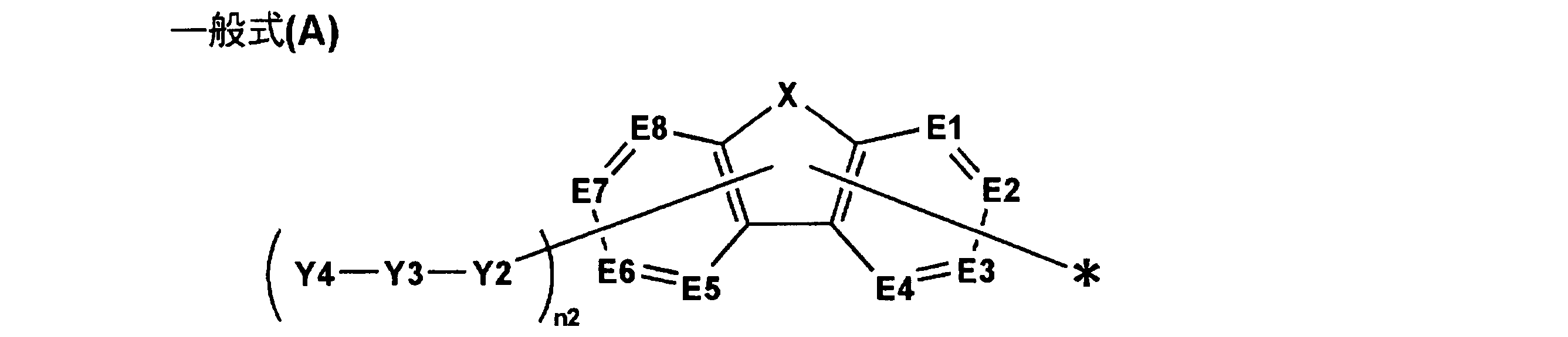
〔式中、n1は1以上の整数を表し、Y1はn1が1の場合は置換基を表し、n1が2以上の場合は単なる結合手又はn1価の連結基を表す。Ar1は下記一般式(A)で表される基を表し、n1が2以上の場合、複数のAr1は同一でも異なっていてもよい。但し、前記一般式(1)で表される化合物は分子内に3環以上の環が縮合してなる縮合芳香族複素環を少なくとも2つ有する。〕
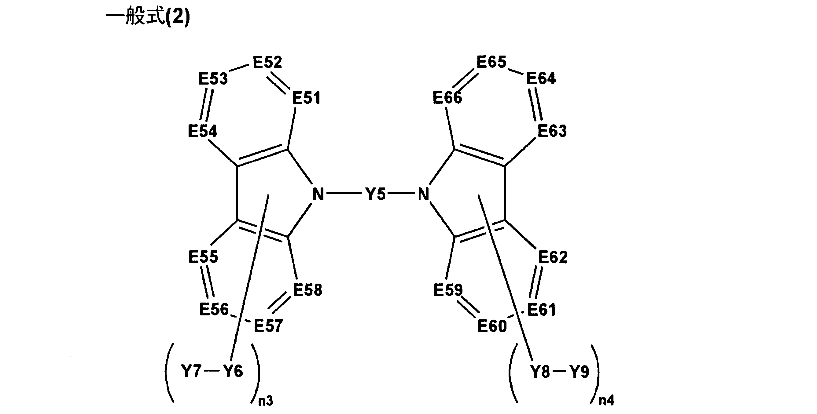
6.前記一般式(1)で表される化合物が、下記一般式(2)で表される化合物であることを特徴とする前記5に記載の有機エレクトロルミネッセンス素子。 Formula (1) (Ar1) n1 -Y1
[Wherein, n1 represents an integer of 1 or more, Y1 represents a substituent when n1 is 1, and represents a single bond or an n1-valent linking group when n1 is 2 or more. Ar1 represents a group represented by the following general formula (A). When n1 is 2 or more, a plurality of Ar1s may be the same or different. However, the compound represented by the general formula (1) has at least two condensed aromatic heterocycles in which three or more rings are condensed in the molecule. ]
6). 6. The organic electroluminescence device as described in 5 above, wherein the compound represented by the general formula (1) is a compound represented by the following general formula (2).
7.前記一般式(2)で表される化合物が、下記一般式(3)で表される化合物であることを特徴とする前記6に記載の有機エレクトロルミネッセンス素子。
7. 7. The organic electroluminescence device as described in 6 above, wherein the compound represented by the general formula (2) is a compound represented by the following general formula (3).

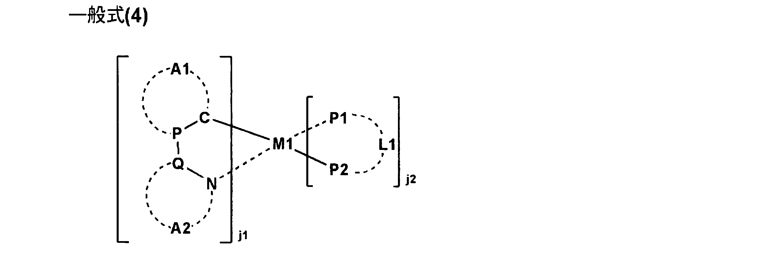
8.前記リン光発光性化合物が下記一般式(4)で表されることを特徴とする前記1~7のいずれか一項に記載の有機エレクトロルミネッセンス素子。
8). 8. The organic electroluminescence device as described in any one of 1 to 7 above, wherein the phosphorescent compound is represented by the following general formula (4).
9.前記一般式(4)で表される化合物が下記一般式(5)で表される化合物であることを特徴とする前記8に記載の有機エレクトロルミネッセンス素子。
9. 9. The organic electroluminescence device as described in 8 above, wherein the compound represented by the general formula (4) is a compound represented by the following general formula (5).

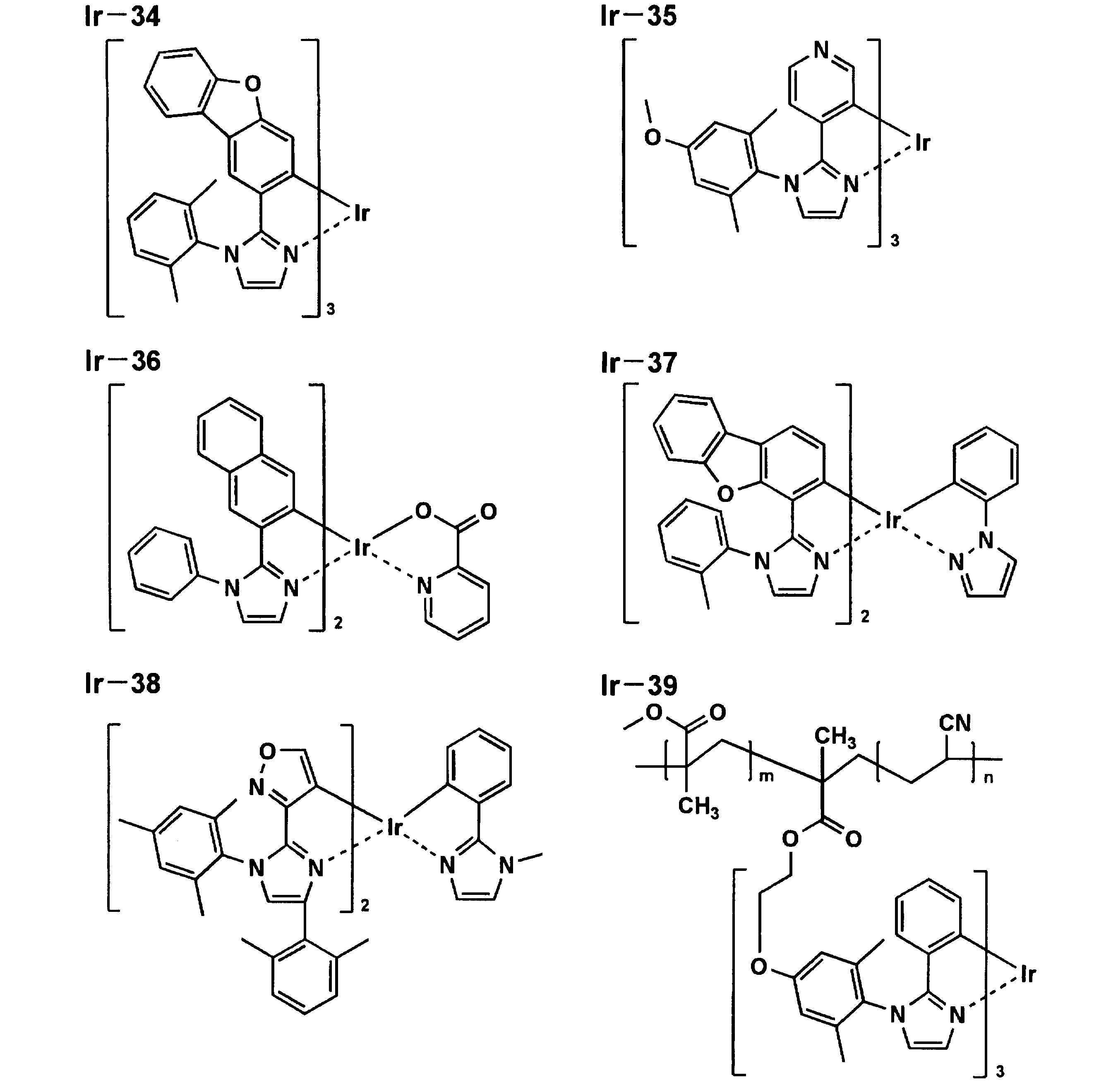
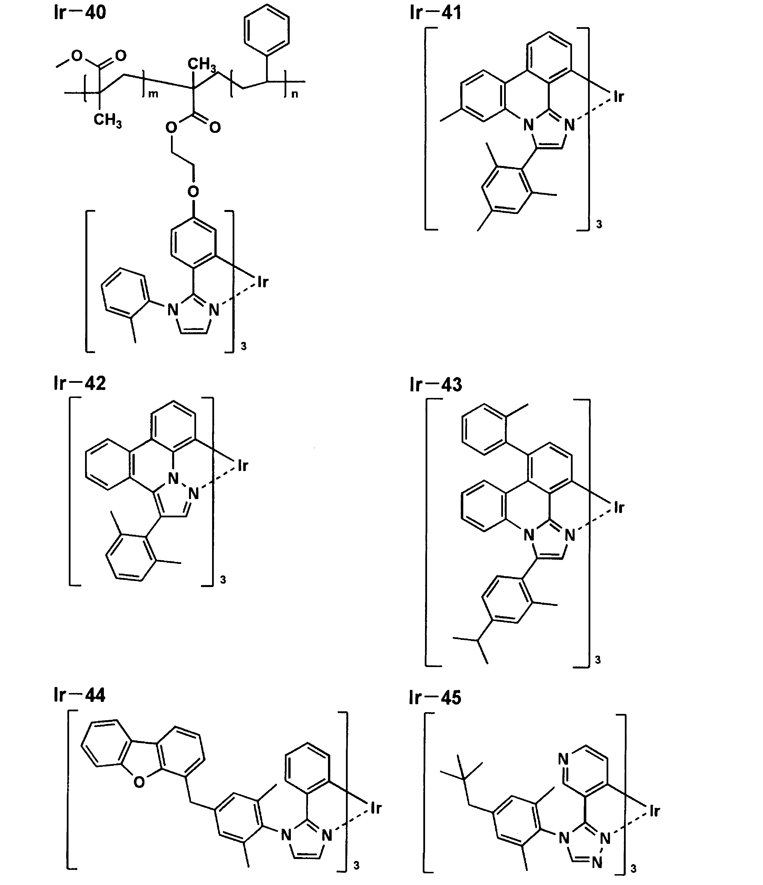
10.前記M1がイリジウムを表すことを特徴とする前記8又は9に記載の有機エレクトロルミネッセンス素子。
10. 10. The organic electroluminescent device according to 8 or 9, wherein M1 represents iridium.
まず、面発光体の一例である本発明の有機EL素子の実施形態を詳細に説明するが、以下に記載する内容は、本発明の実施態様の代表例であり、本発明はその要旨を超えない限り、これらの内容に限定されない。 << Organic EL element >>
First, embodiments of the organic EL device of the present invention, which is an example of a surface light emitter, will be described in detail. The contents described below are representative examples of embodiments of the present invention, and the present invention exceeds the gist thereof. As long as there is no, it is not limited to these contents.
(ii)陽極/正孔注入層/正孔輸送層/発光層/電子輸送層/電子注入層/透明保護層/陰極
(iii)陽極/正孔輸送層/発光層/正孔阻止層/電子輸送層/電子注入層/透明保護層/陰極
(iv)陽極/透明保護層/正孔注入層/正孔輸送層/発光層/電子輸送層/電子注入層/陰極
(v)陽極/透明保護層/正孔輸送層/発光層/正孔阻止層/電子輸送層/電子注入層/陰極
本発明の有機EL素子は透明保護層の後に形成する電極が透明導電性層であることを特徴とし、対向する電極はアプリケーションによって透明、不透明のどちらも選択することができる。本発明の有機EL素子はトップエミッション型又は両面エミッション型の構成を取ることが好ましい。 (I) Anode / light emitting layer / electron transport layer / electron injection layer / transparent protective layer / cathode (ii) Anode / hole injection layer / hole transport layer / light emitting layer / electron transport layer / electron injection layer / transparent protective layer / Cathode (iii) Anode / hole transport layer / light emitting layer / hole blocking layer / electron transport layer / electron injection layer / transparent protective layer / cathode (iv) Anode / transparent protective layer / hole injection layer / hole transport Layer / light emitting layer / electron transport layer / electron injection layer / cathode (v) anode / transparent protective layer / hole transport layer / light emitting layer / hole blocking layer / electron transport layer / electron injection layer / cathode Organic EL of the present invention The element is characterized in that the electrode formed after the transparent protective layer is a transparent conductive layer, and the opposite electrode can be selected from transparent and opaque depending on the application. The organic EL device of the present invention preferably has a top emission type or double side emission type configuration.
本発明に係る透明保護層とは、実質的に透明であり、かつ透明保護層の後工程での発光層へのプロセスダメージを抑制する層であることを特徴とする。本発明でいう実質的に透明とは可視光透過率が50%以上のことを指す。 《Transparent protective layer》
The transparent protective layer according to the present invention is a layer that is substantially transparent and suppresses process damage to the light emitting layer in a subsequent step of the transparent protective layer. The term “substantially transparent” as used in the present invention means that the visible light transmittance is 50% or more.
本発明の有機EL素子は、透明導電性層上に抵抗を下げる目的で補助電極を設けることができる。補助電極を形成する材料としては、金、白金、銀、銅、アルミ等の抵抗が低い金属が好ましい。補助電極の形成方法としては、蒸着法、スパッタリング法、印刷法、インクジェット法、エアロゾルジェット法などが挙げられる。本発明に係る補助電極の線幅は透明導電性層の開口率の観点から50μm以下であることが好ましく、補助電極の厚さは導電性の観点から、1μ以上であることが好ましい。本発明に係る補助電極は透明保護層がパターニングされている場合は、透明保護層のパターニングされていない領域上に形成することが好ましい。本発明でいう、透明保護層のパターニングされていない領域とは透明保護層がない領域上のことを指す。 《Auxiliary electrode》
In the organic EL device of the present invention, an auxiliary electrode can be provided on the transparent conductive layer for the purpose of reducing the resistance. As a material for forming the auxiliary electrode, a metal having low resistance such as gold, platinum, silver, copper, and aluminum is preferable. Examples of the method for forming the auxiliary electrode include a vapor deposition method, a sputtering method, a printing method, an ink jet method, and an aerosol jet method. The line width of the auxiliary electrode according to the present invention is preferably 50 μm or less from the viewpoint of the aperture ratio of the transparent conductive layer, and the thickness of the auxiliary electrode is preferably 1 μm or more from the viewpoint of conductivity. When the transparent protective layer is patterned, the auxiliary electrode according to the present invention is preferably formed on an unpatterned region of the transparent protective layer. In the present invention, the region where the transparent protective layer is not patterned refers to the region where there is no transparent protective layer.
本発明に係る有機EL素子における透明導電性層としては、インジウムチンオキシド(ITO)、SnO2、ZnO等の導電性光透過性材料が好ましく用いられる。また、IDIXO(In2O3-ZnO)等非晶質で光透過性の導電膜を作製可能な材料を用いてもよい。本発明に係る透明導電性層の形成方法としては生産性の観点から、スパッタリング法が好ましい。本発明に係る透明導電性層は必要に応じて、フォトリソグラフィー法で所望の形状のパターンを形成してもよく、あるいはパターン精度を余り必要としない場合は(100μm以上程度)、上記電極物質の蒸着やスパッタリング時に所望の形状のマスクを介してパターンを形成してもよい。本発明に係る透明導電性層のシート抵抗は数百Ω/□以下が好ましい。更に膜厚は材料にもよるが、通常10~1000nm、好ましくは50~200nmの範囲で選ばれる。 << Transparent conductive layer: Electrode >>
As the transparent conductive layer in the organic EL device according to the present invention, a conductive light transmissive material such as indium tin oxide (ITO), SnO 2 , ZnO or the like is preferably used. Alternatively, a material such as IDIXO (In 2 O 3 —ZnO) that can form an amorphous light-transmitting conductive film may be used. As a method for forming the transparent conductive layer according to the present invention, a sputtering method is preferable from the viewpoint of productivity. If necessary, the transparent conductive layer according to the present invention may form a pattern having a desired shape by photolithography, or if the pattern accuracy is not so high (about 100 μm or more), A pattern may be formed through a mask having a desired shape during vapor deposition or sputtering. The sheet resistance of the transparent conductive layer according to the present invention is preferably several hundred Ω / □ or less. Further, although the film thickness depends on the material, it is usually selected in the range of 10 to 1000 nm, preferably 50 to 200 nm.
本発明に係る発光層は発光材料としてリン光発光性化合物が含有されていることを特徴とする。 [Light emitting layer]
The light emitting layer according to the present invention is characterized in that a phosphorescent compound is contained as a light emitting material.
有機EL素子の発光層に含有されるホスト化合物としては、室温(25℃)における燐光発光の燐光量子収率が0.1未満の化合物が好ましい。更に好ましくは燐光量子収率が0.01未満である。また、発光層に含有される化合物の中で、その層中での体積比が50%以上であることが好ましい。 <Host compound>
As the host compound contained in the light emitting layer of the organic EL device, a compound having a phosphorescence quantum yield of phosphorescence emission at room temperature (25 ° C.) of less than 0.1 is preferable. More preferably, the phosphorescence quantum yield is less than 0.01. Moreover, it is preferable that the volume ratio in the layer is 50% or more among the compounds contained in a light emitting layer.
次に、発光材料について説明する。 <Light emitting material>
Next, the light emitting material will be described.
本発明の有機EL素子に係るリン光発光性化合物としては、上記一般式(4)で表される化合物が好ましい。 << Compound Represented by Formula (4) >>
As the phosphorescent compound according to the organic EL device of the present invention, a compound represented by the general formula (4) is preferable.
本発明に係る一般式(4)で表される化合物の中でも、一般式(5)で表される化合物が好ましい。 << Compound Represented by Formula (5) >>
Among the compounds represented by the general formula (4) according to the present invention, the compound represented by the general formula (5) is preferable.


各発光層間に非発光性の中間層(非ドープ領域等ともいう)を設ける場合について説明する。 [Middle layer]
A case where a non-light emitting intermediate layer (also referred to as an undoped region or the like) is provided between the light emitting layers will be described.
注入層は必要に応じて設け、電子注入層と正孔注入層があり、上記の如く陽極と発光層又は正孔輸送層の間、及び陰極と発光層又は電子輸送層との間に存在させてもよい。 [Injection layer: electron injection layer, hole injection layer]
The injection layer is provided as necessary, and there are an electron injection layer and a hole injection layer, and as described above, it exists between the anode and the light emitting layer or the hole transport layer, and between the cathode and the light emitting layer or the electron transport layer. May be.
阻止層は、上記の如く有機化合物薄膜の基本構成層のほかに必要に応じて設けられるものである。例えば、特開平11-204258号公報、同11-204359号公報、及び「有機EL素子とその工業化最前線(1998年11月30日エヌ・ティー・エス社発行)」の237頁等に記載されている正孔阻止(ホールブロック)層がある。 [Blocking layer: hole blocking layer, electron blocking layer]
The blocking layer is provided as necessary in addition to the basic constituent layer of the organic compound thin film as described above. For example, it is described in JP-A Nos. 11-204258 and 11-204359, and “Organic EL elements and the forefront of industrialization (published by NTT Corporation on November 30, 1998)” on page 237. There is a hole blocking (hole blocking) layer.
正孔輸送層とは、正孔を輸送する機能を有する正孔輸送材料からなり、広い意味で正孔注入層、電子阻止層も正孔輸送層に含まれる。正孔輸送層は単層又は複数層設けることができる。 (Hole transport layer)
The hole transport layer is made of a hole transport material having a function of transporting holes, and in a broad sense, a hole injection layer and an electron blocking layer are also included in the hole transport layer. The hole transport layer can be provided as a single layer or a plurality of layers.
電子輸送層とは、電子を輸送する機能を有する材料からなり、広い意味で電子注入層、正孔阻止層も電子輸送層に含まれる。電子輸送層は単層又は複数層設けることができる。 (Electron transport layer)
The electron transport layer is made of a material having a function of transporting electrons, and in a broad sense, an electron injection layer and a hole blocking layer are also included in the electron transport layer. The electron transport layer can be provided as a single layer or a plurality of layers.
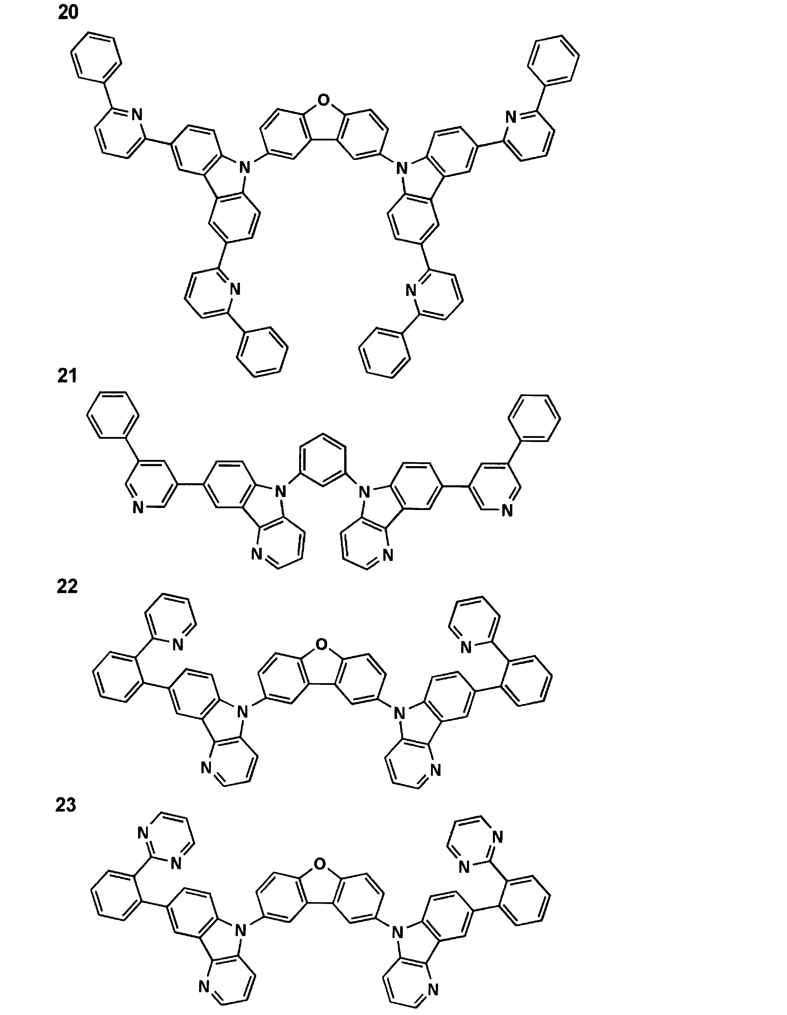
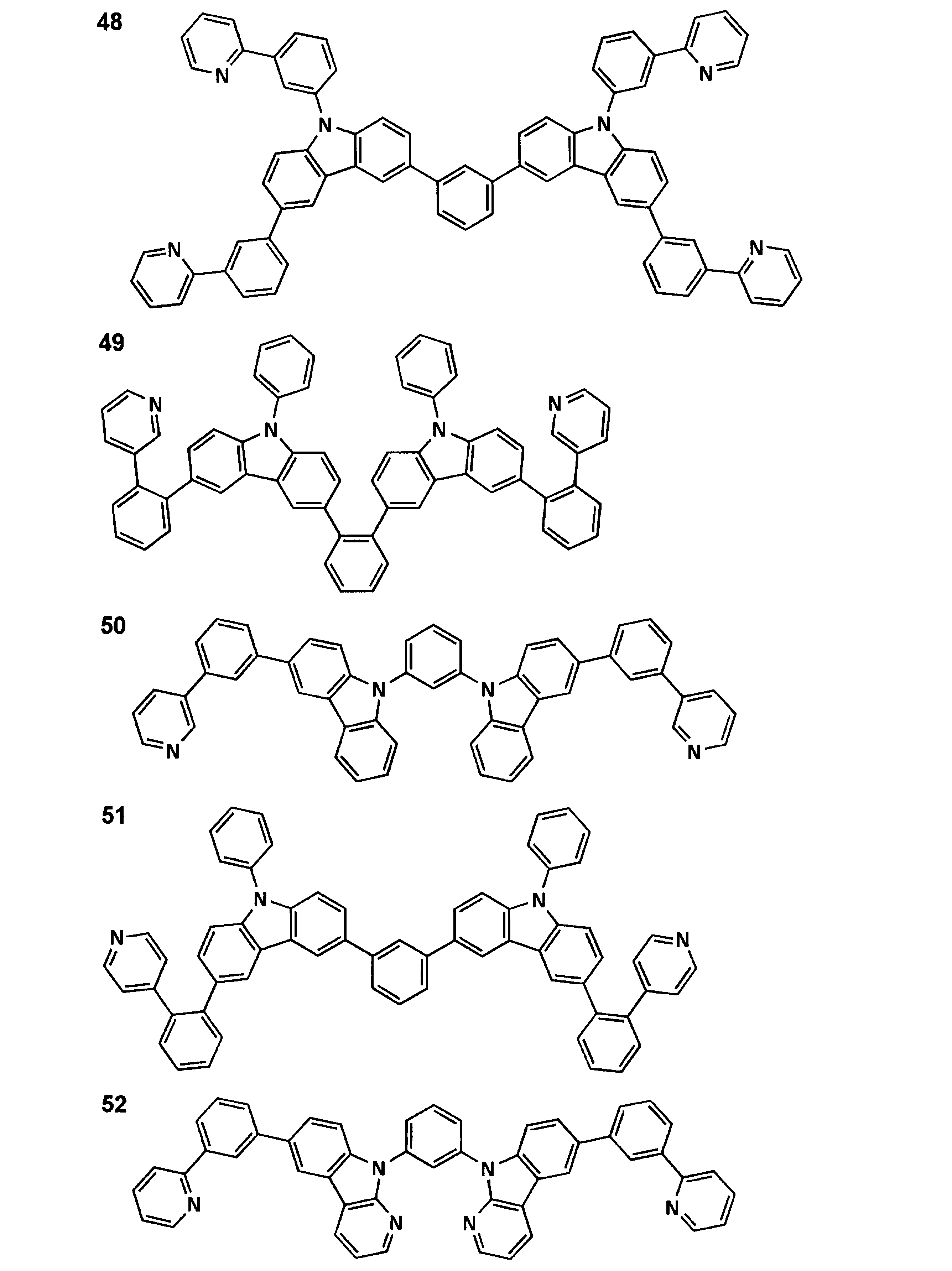
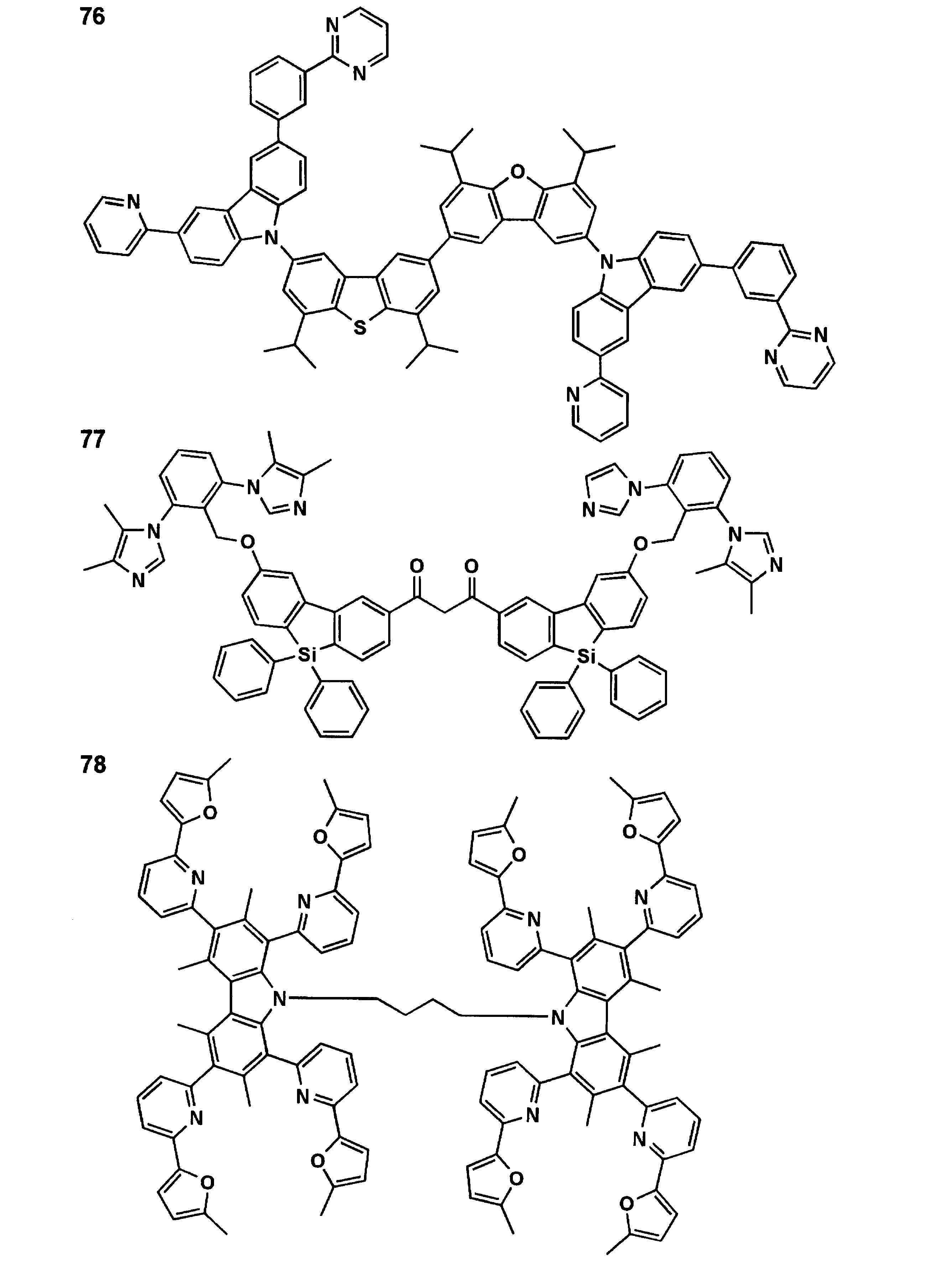
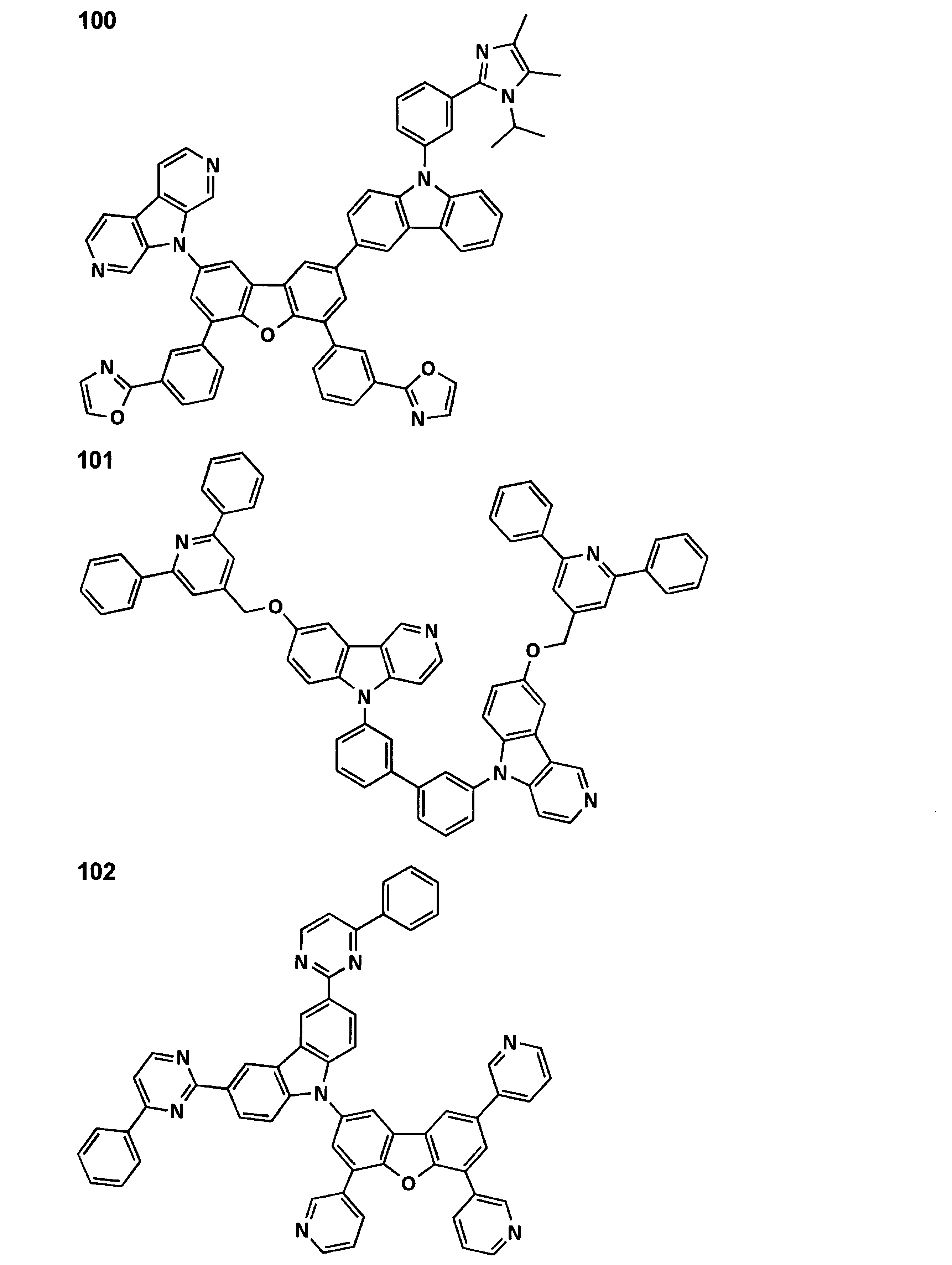
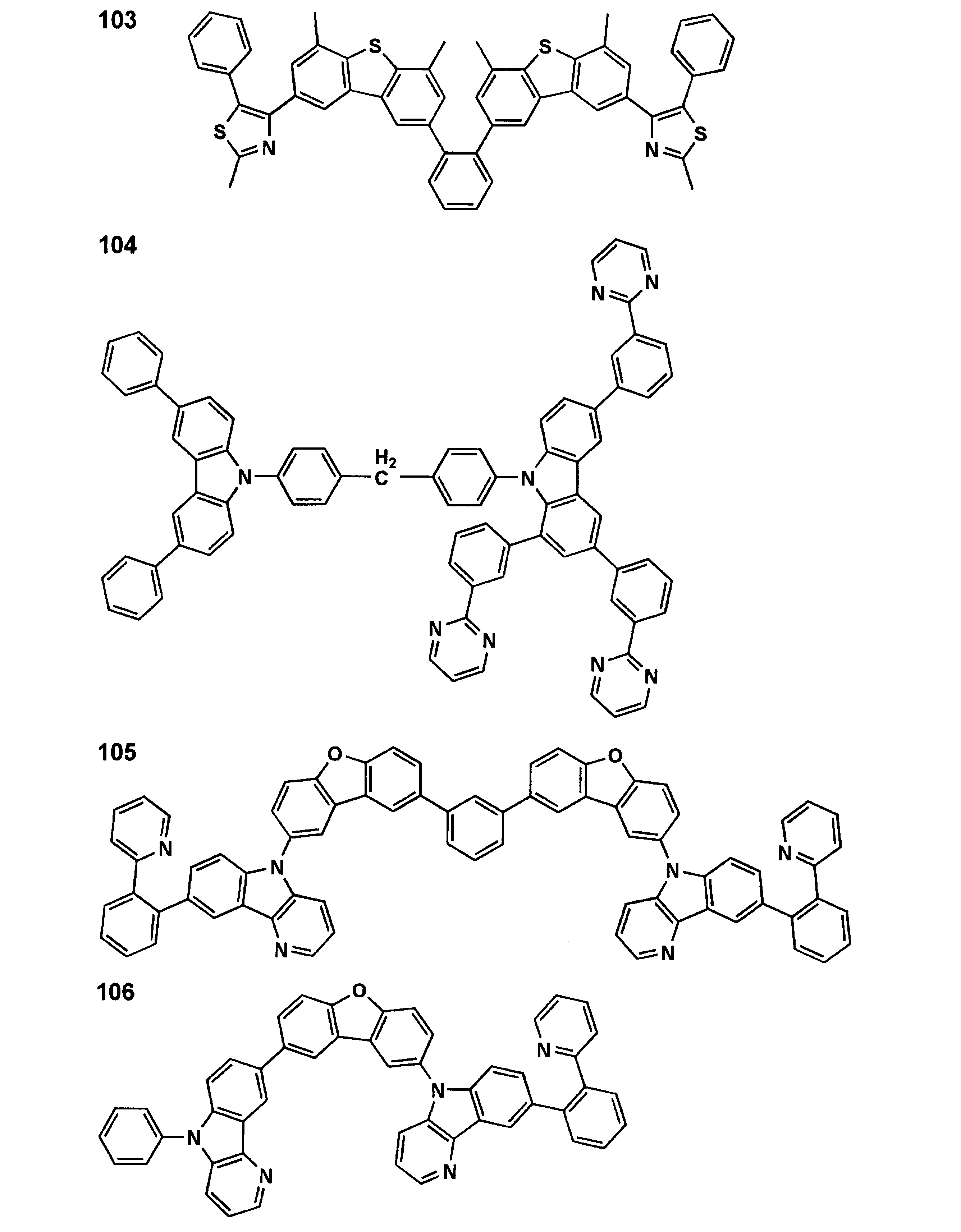
本発明に係る一般式(1)で表される化合物について説明する。 << Compound Represented by Formula (1) >>
The compound represented by the general formula (1) according to the present invention will be described.
一般式(1)において、Ar1は、前記一般式(A)で表される基を表す。 (Group represented by general formula (A))
In the general formula (1), Ar1 represents a group represented by the general formula (A).
一般式(A)において、Y3で表される基としては、上記6員の芳香族環から導出される基であることが好ましく、更に好ましくは、ベンゼン環から導出される基である。 (Preferred embodiment of the group represented by Y3)
In the general formula (A), the group represented by Y3 is preferably a group derived from the above 6-membered aromatic ring, and more preferably a group derived from a benzene ring.
一般式(A)において、Y4で表される基としては、上記6員の芳香族環から導出される基であることが好ましく、更に好ましくは、窒素原子を環構成原子と含む芳香族複素環から導出される基であり、特に好ましくは、Y4がピリジン環から導出される基であることである。 (Preferred embodiment of the group represented by Y4)
In general formula (A), the group represented by Y4 is preferably a group derived from the 6-membered aromatic ring, more preferably an aromatic heterocycle containing a nitrogen atom as a ring constituent atom. Particularly preferably, Y4 is a group derived from a pyridine ring.
一般式(A)で表される基の好ましい態様としては、下記一般式(A-1)、(A-2)、(A-3)又は(A-4)のいずれかで表される基が挙げられる。 (Preferred embodiment of the group represented by the general formula (A))
As a preferred embodiment of the group represented by the general formula (A), a group represented by any of the following general formulas (A-1), (A-2), (A-3) or (A-4) Is mentioned.


本発明では、上記一般式(1)で表される化合物の中でも、上記一般式(2)で表される化合物が好ましい。以下、一般式(2)で表される化合物について説明する。 << Compound Represented by Formula (2) >>
In this invention, the compound represented by the said General formula (2) is preferable among the compounds represented by the said General formula (1). Hereinafter, the compound represented by the general formula (2) will be described.
以下、一般式(2)で表される化合物について説明する。 << Compound Represented by Formula (3) >>
Hereinafter, the compound represented by the general formula (2) will be described.


窒素雰囲気下、3,6-ジブロモジベンゾフラン(1.0モル)、カルバゾール(2.0モル)、銅粉末(3.0モル)、炭酸カリウム(1.5モル)をDMAc(ジメチルアセトアミド)300ml中に混合し、130℃で24時間撹拌した。反応液を室温まで冷却後、トルエン1lを加え、蒸留水で3回洗浄し、有機層を減圧下に溶媒を留去し、残渣をシリカゲルフラッシュクロマトグラフィー(n-ヘプタン:トルエン=4:1~3:1)にて精製し、中間体1を収率85%で得た。 << Synthesis Example of
Under a nitrogen atmosphere, 3,6-dibromodibenzofuran (1.0 mol), carbazole (2.0 mol), copper powder (3.0 mol) and potassium carbonate (1.5 mol) in 300 ml of DMAc (dimethylacetamide) And stirred at 130 ° C. for 24 hours. After cooling the reaction solution to room temperature, 1 l of toluene was added, washed with distilled water three times, the organic layer was evaporated under reduced pressure, and the residue was subjected to silica gel flash chromatography (n-heptane: toluene = 4: 1˜ 3: 1) to obtain
室温、大気下で中間体1(0.5モル)をDMF100mlに溶解し、NBS(2.0モル)を加え、一晩室温で撹拌した。得られた沈殿を濾過し、メタノールで洗浄し、中間体2を収率92%で得た。 Step 2: (Synthesis of Intermediate 2)
Intermediate 1 (0.5 mol) was dissolved in 100 ml of DMF at room temperature under air, NBS (2.0 mol) was added, and the mixture was stirred overnight at room temperature. The resulting precipitate was filtered and washed with methanol, yielding intermediate 2 in 92% yield.
窒素雰囲気下、中間体2(0.25モル)、2-フェニルピリジン(1.0モル)、ルテニウム錯体[(η6-C6H6)RuCl2]2(0.05モル)、トリフェニルホスフィン(0.2モル)、炭酸カリウム(12モル)をNMP(N-メチル-2-ピロリドン)3l中で混合し、140℃で一晩撹拌した。 Step 3: (Synthesis of Compound 5)
Under nitrogen atmosphere, intermediate 2 (0.25 mol), 2-phenylpyridine (1.0 mol), ruthenium complex [(η6-C 6 H 6 ) RuCl 2 ] 2 (0.05 mol), triphenylphosphine (0.2 mol) and potassium carbonate (12 mol) were mixed in 3 l of NMP (N-methyl-2-pyrrolidone) and stirred at 140 ° C. overnight.
対向電極としては、前述の透明導電性を構成する材料を用いても良いし、金属、合金、電気伝導性化合物及びこれらの混合物を電極物質とするものが用いることもできる。このような電極物質の具体例としては、ナトリウム、ナトリウム-カリウム合金、マグネシウム、リチウム、マグネシウム/銅混合物、マグネシウム/銀混合物、マグネシウム/アルミニウム混合物、マグネシウム/インジウム混合物、アルミニウム/酸化アルミニウム(Al2O3)混合物、インジウム、リチウム/アルミニウム混合物、希土類金属等が挙げられる。対向電極はこれらの電極物質を蒸着やスパッタリング等の方法により薄膜を形成させることにより、作製することができる。また、対向電極としてのシート抵抗は数百Ω/□以下が好ましく、膜厚は通常10nm~5μm、好ましくは50nm~200nmの範囲で選ばれる。 [Counter electrode: anode or cathode]
As the counter electrode, the above-described material constituting the transparent conductivity may be used, or an electrode material made of a metal, an alloy, an electrically conductive compound, or a mixture thereof may be used. Specific examples of such electrode materials include sodium, sodium-potassium alloy, magnesium, lithium, magnesium / copper mixture, magnesium / silver mixture, magnesium / aluminum mixture, magnesium / indium mixture, aluminum / aluminum oxide (Al 2 O 3 ) Mixtures, indium, lithium / aluminum mixtures, rare earth metals and the like. The counter electrode can be produced by forming a thin film of these electrode materials by a method such as vapor deposition or sputtering. The sheet resistance as the counter electrode is preferably several hundred Ω / □ or less, and the film thickness is usually selected in the range of 10 nm to 5 μm, preferably 50 nm to 200 nm.
本発明の有機EL素子は、表示デバイス、ディスプレイ、各種発光光源として用いることができる。発光光源として、例えば、家庭用照明、車内照明、時計や液晶用のバックライト、看板広告、信号機、光記憶媒体の光源、電子写真複写機の光源、光通信処理機の光源、光センサーの光源等が挙げられるがこれに限定するものではないが、特にカラーフィルターと組み合わせた液晶表示装置のバックライト、照明用光源としての用途に有効に用いることができる。 <Application>
The organic EL element of the present invention can be used as a display device, a display, and various light emission sources. Examples of light sources include home lighting, interior lighting, clock and liquid crystal backlights, billboard advertisements, traffic lights, light sources for optical storage media, light sources for electrophotographic copying machines, light sources for optical communication processors, and light sources for optical sensors. Although it is not limited to this, it can be effectively used for a backlight of a liquid crystal display device combined with a color filter and a light source for illumination.
有機EL素子1-1~1-26は発光面積が5cm×5cmとなるように作製した。 << Production of double-sided emission type organic EL elements >>
The organic EL elements 1-1 to 1-26 were fabricated so that the light emitting area was 5 cm × 5 cm.
(陽極の形成)
透明な基板1の上に厚さ100nmとなる条件でITOをスパッタ法で成膜、パターニングして、ITO層から成る陽極を形成した。次いで、ITO層を設けた基板を、イソプロピルアルコールで超音波洗浄し、乾燥窒素ガスで乾燥し、UVオゾン洗浄を5分間行った。 [Production of Organic EL Element 1-1]
(Formation of anode)
On the
このITO層を設けた基板を市販の真空蒸着装置の基板ホルダーに固定し、タンタル製抵抗加熱ボートに下記のα-NPD、DPVBi、BAlq、Alq3及びフッ化カリウムをそれぞれ入れ、真空蒸着装置の第1真空槽に取り付けた。 (Formation of hole injection layer to electron transport layer)
The substrate provided with the ITO layer is fixed to a substrate holder of a commercially available vacuum deposition apparatus, and the following α-NPD, DPVBi, BAlq, Alq 3 and potassium fluoride are placed in a tantalum resistance heating boat, respectively. Attached to the first vacuum chamber.

次に、フッ化カリウムの入った前記加熱ボートに通電して加熱し、蒸着速度0.01~0.02nm/秒で膜厚1nmのフッ化カリウム層を設けた。更に、フッ化カリウム層まで成膜した素子を真空のまま第2真空槽に移し、第2真空槽を4×10-4Paまで減圧した後、アルミニウムの入った前記加熱ボートに通電して、蒸着速度0.1~0.2nm/秒で膜厚5nmのアルミニウム層を形成し、電子注入層を設けた。 (Formation of electron injection layer)
Next, the heating boat containing potassium fluoride was energized and heated to provide a potassium fluoride layer having a thickness of 1 nm at a deposition rate of 0.01 to 0.02 nm / sec. Further, the element formed up to the potassium fluoride layer was transferred to the second vacuum chamber in a vacuum, the second vacuum chamber was depressurized to 4 × 10 −4 Pa, and then the heating boat containing aluminum was energized, An aluminum layer having a film thickness of 5 nm was formed at a deposition rate of 0.1 to 0.2 nm / second, and an electron injection layer was provided.
次に、電子注入層まで成膜した素子をあらかじめITOターゲットを装着した市販の平行平板スパッタリング装置に移し、スパッタリング装置のチャンバー内を5×10⁻³Paまで減圧した後、窒素ガスと酸素ガスを流しながら、DC出力500Wで放電し、成膜速度10nm/秒で膜厚100nmのITO導電層の透明導電性層(陰極)を形成した。 (Formation of transparent conductive layer (cathode))
Next, the element formed up to the electron injection layer was transferred to a commercially available parallel plate sputtering apparatus equipped with an ITO target in advance, and the pressure in the chamber of the sputtering apparatus was reduced to 5 × 10 −3 Pa, and then nitrogen gas and oxygen gas were added. While flowing, discharge was performed at a DC output of 500 W, and a transparent conductive layer (cathode) of an ITO conductive layer having a film thickness of 10 nm / second and a film thickness of 100 nm was formed.
最後に、上記で得られた素子をガラスケースで覆い、厚み300μmのガラス基板を封止用基板として用い、周囲にシール材としてエポキシ系光硬化型接着剤(東亞合成社製ラックストラックLC0629B)を適用し、これを前記透明支持基板と密着させ、ガラス基板側からUV光を照射して、硬化・封止して、両面エミッション型有機EL素子1-1を得た。 (Element sealing)
Finally, the device obtained above is covered with a glass case, a glass substrate having a thickness of 300 μm is used as a sealing substrate, and an epoxy-based photocurable adhesive (Lux Track LC0629B, manufactured by Toagosei Co., Ltd.) is used as a sealing material around it. This was applied and brought into close contact with the transparent support substrate, irradiated with UV light from the glass substrate side, cured and sealed to obtain a double-sided emission type organic EL device 1-1.
(陽極~電子注入層の形成)
陽極~電子注入層までは有機EL素子1-1と同様な方法で成膜した。 [Production of Organic EL Element 1-2]
(Formation of anode to electron injection layer)
The layers from the anode to the electron injection layer were formed by the same method as the organic EL element 1-1.
次に、電子注入層まで成膜した素子を真空のまま第1真空槽に戻し、第1真空槽を4×10⁻⁴Paまで減圧した後、真空蒸着装置に酸素ガスを導入せずに、酸化カルシウムCaOの入った加熱ボートに通電して加熱し、蒸着速度0.1~0.2nm/秒で膜厚20nmの透明保護層を設けた。なお、同様な方法で作製した素子を別途作製し、透明保護層をESCAで分析したところ、透明保護層を構成している酸化カルシウムは酸素欠陥状態(非化学量論組成)になっていた。 (Formation of transparent protective layer)
Next, the element formed up to the electron injection layer was returned to the first vacuum chamber while being vacuumed, and after the first vacuum chamber was depressurized to 4 × 10 −4 Pa, oxygen gas was not introduced into the vacuum deposition apparatus, A heating boat containing calcium oxide CaO was energized and heated to provide a transparent protective layer having a thickness of 20 nm at a deposition rate of 0.1 to 0.2 nm / second. In addition, when the element produced with the same method was produced separately and the transparent protective layer was analyzed by ESCA, the calcium oxide which comprises the transparent protective layer was in an oxygen defect state (non-stoichiometric composition).
有機EL素子1-1と同様にして陰極を成膜した。 (Formation of cathode)
A cathode was formed in the same manner as in the organic EL element 1-1.
有機EL素子1-1と同様な方法で硬化・封止して、両面エミッション型有機EL素子1-2を得た。 (Element sealing)
Curing and sealing were performed in the same manner as for the organic EL element 1-1 to obtain a double-sided emission type organic EL element 1-2.
透明保護層の膜厚を20nmから70nmに変更した以外は有機EL素子1-2と同様な方法で両面エミッション型有機EL素子1-3を得た。 [Production of Organic EL Element 1-3]
A double-sided emission type EL device 1-3 was obtained in the same manner as the organic EL device 1-2 except that the thickness of the transparent protective layer was changed from 20 nm to 70 nm.
透明保護層の材料を酸化カルシウムから酸化ランタンに変更した以外は有機EL素子1-2と同様な方法で両面エミッション型有機EL素子1-4を得た。 [Production of Organic EL Element 1-4]
A double-sided emission type organic EL element 1-4 was obtained in the same manner as the organic EL element 1-2 except that the material of the transparent protective layer was changed from calcium oxide to lanthanum oxide.
透明保護層の膜厚を20nmから70nmに変更した以外は有機EL素子1-4と同様な方法で両面エミッション型有機EL素子1-5を得た。 [Production of Organic EL Element 1-5]
A double-sided emission type organic EL device 1-5 was obtained in the same manner as the organic EL device 1-4 except that the film thickness of the transparent protective layer was changed from 20 nm to 70 nm.
(陽極の形成)
有機EL素子1-1と同様な方法でITO層から成る陽極を形成した。 [Production of Organic EL Element 1-6]
(Formation of anode)
An anode made of an ITO layer was formed in the same manner as in the organic EL element 1-1.
このITO層を設けた基板を市販の真空蒸着装置の基板ホルダーに固定し、タンタル製抵抗加熱ボートに前記α-NPD、H4、Ir-4、BAlq、Alq3及び酸化バナジウムをそれぞれ入れ、真空蒸着装置の第1真空槽に取り付けた。 (Formation of hole injection layer to electron transport layer)
The substrate provided with the ITO layer is fixed to a substrate holder of a commercially available vacuum deposition apparatus, and the α-NPD, H4, Ir-4, BAlq, Alq 3 and vanadium oxide are placed in a tantalum resistance heating boat, respectively, and vacuum deposition is performed. Attached to the first vacuum chamber of the apparatus.
次に、フッ化カリウムの入った前記加熱ボートに通電して加熱し、蒸着速度0.01~0.02nm/秒で膜厚1nmのフッ化カリウム層を設けた。更に、フッ化カリウム層まで成膜した素子を真空のまま第2真空槽に移し、第2真空槽を4×10-4Paまで減圧した後、アルミニウムの入った前記加熱ボートに通電して、蒸着速度0.1~0.1~0.2nm/秒で膜厚5nmのアルミニウム層を形成し、電子注入層を設けた。 (Formation of electron injection layer)
Next, the heating boat containing potassium fluoride was energized and heated to provide a potassium fluoride layer having a thickness of 1 nm at a deposition rate of 0.01 to 0.02 nm / sec. Further, the element formed up to the potassium fluoride layer was transferred to the second vacuum chamber in a vacuum, the second vacuum chamber was depressurized to 4 × 10 −4 Pa, and then the heating boat containing aluminum was energized, An aluminum layer having a film thickness of 5 nm was formed at a deposition rate of 0.1 to 0.1 to 0.2 nm / second, and an electron injection layer was provided.
次に、電子注入層まで成膜した素子を真空のまま第1真空槽に戻し、第1真空槽を4×10⁻⁴Paまで減圧した後、酸化バナジウムの入った前記加熱ボートに通電して加熱し、蒸着速度0.1~0.2nm/秒で蒸着して膜厚20nmの透明保護層を設けた。 (Formation of transparent protective layer)
Next, the element formed up to the electron injection layer is returned to the first vacuum chamber while being vacuumed, and the first vacuum chamber is depressurized to 4 × 10 −4 Pa, and then the heating boat containing vanadium oxide is energized. The film was heated and evaporated at a deposition rate of 0.1 to 0.2 nm / second to provide a 20 nm thick transparent protective layer.
次に、透明保護層まで成膜した素子をあらかじめITOターゲットを装着した市販の平行平板スパッタリング装置に移し、スパッタリング装置のチャンバー内を5×10⁻³Paまで減圧した後、窒素ガスと酸素ガスを流しながら、DC出力500Wで放電し、成膜速度10nm/秒で膜厚100nmのITO導電層の透明導電性層(陰極)を形成した。 (Formation of transparent conductive layer (cathode))
Next, the element formed up to the transparent protective layer was transferred to a commercially available parallel plate sputtering apparatus equipped with an ITO target in advance, and after reducing the pressure in the sputtering apparatus chamber to 5 × 10 −3 Pa, nitrogen gas and oxygen gas were added. While flowing, discharge was performed at a DC output of 500 W, and a transparent conductive layer (cathode) of an ITO conductive layer having a film thickness of 10 nm / second and a film thickness of 100 nm was formed.
有機EL素子1-1と同様な方法で硬化・封止して、両面エミッション型有機EL素子1-6を得た。 (Element sealing)
It was cured and sealed in the same manner as the organic EL element 1-1 to obtain a double-sided emission type organic EL element 1-6.
(陽極~電子注入層の形成)
陽極~電子注入層までは有機EL素子1-6と同様な方法で成膜した。 [Production of Organic EL Element 1-7]
(Formation of anode to electron injection layer)
The layers from the anode to the electron injection layer were formed by the same method as for the organic EL element 1-6.
次に、電子注入層まで成膜した素子を真空のまま第1真空槽に戻し、第1真空槽を4×10⁻⁴Paまで減圧した後、酸化モリブデン(6価)の入った加熱ボートに通電して加熱し、蒸着速度0.1~0.2nm/秒で蒸着を行い膜厚20nmの透明保護層を設けた。 (Formation of transparent protective layer)
Next, the element formed up to the electron injection layer was returned to the first vacuum chamber while being vacuumed, and the first vacuum chamber was depressurized to 4 × 10 −4 Pa, and then placed on a heating boat containing molybdenum oxide (hexavalent). Heating was performed by energization, and deposition was performed at a deposition rate of 0.1 to 0.2 nm / second to provide a 20 nm thick transparent protective layer.
有機EL素子1-6と同様にして陰極を成膜した。 (Formation of cathode)
A cathode was formed in the same manner as in the organic EL element 1-6.
有機EL素子1-6と同様な方法で硬化・封止して、両面エミッション型有機EL素子1-7を得た。なお、同様な方法で作製した素子を別途作製し、透明保護層をESCAで分析し、透明保護層を構成している酸化モリブデン(6価)は酸素欠陥状態になっていることを確認した。 (Element sealing)
Curing and sealing were performed in the same manner as for organic EL element 1-6 to obtain double-sided emission type organic EL element 1-7. In addition, the element produced by the same method was produced separately, and the transparent protective layer was analyzed by ESCA, and it was confirmed that molybdenum oxide (hexavalent) constituting the transparent protective layer was in an oxygen defect state.
透明保護層の膜厚を表1に記載の値に変更した以外は有機EL素子1-7と同様な方法で、有機EL素子1-8~1-12を作製した。 [Production of Organic EL Elements 1-8 to 1-12]
Organic EL elements 1-8 to 1-12 were produced in the same manner as the organic EL element 1-7, except that the thickness of the transparent protective layer was changed to the values shown in Table 1.
電子輸送層の化合物を表1に記載の化合物に変更した以外は有機EL素子1-9と同様な方法で、有機EL素子1-13~1-15を作製した。 [Production of Organic EL Elements 1-13 to 1-15]
Organic EL devices 1-13 to 1-15 were produced in the same manner as the organic EL device 1-9, except that the compounds in the electron transport layer were changed to the compounds shown in Table 1.
リン光発光性化合物を表1に記載の化合物に変更した以外は有機EL素子1-15と同様な方法で、有機EL素子1-16~1-18を作製した。 [Production of Organic EL Elements 1-16 to 1-18]
Organic EL devices 1-16 to 1-18 were produced in the same manner as the organic EL device 1-15 except that the phosphorescent compound was changed to the compounds shown in Table 1.
透明保護層の材料を表1に記載の材料に変更した以外は有機EL素子1-18と同様な方法で、有機EL素子1-19~1-20を作製した。なお、表1に記した酸化モリブデンは6価であり、酸化レニウムは6価であり、酸化ニッケルは2価である。 [Production of Organic EL Elements 1-19 to 1-20]
Organic EL elements 1-19 to 1-20 were produced in the same manner as the organic EL element 1-18, except that the material of the transparent protective layer was changed to the material shown in Table 1. Note that molybdenum oxide shown in Table 1 is hexavalent, rhenium oxide is hexavalent, and nickel oxide is divalent.
(陽極~陰極の形成)
陽極~陰極までは有機EL素子1-18と同様な方法で成膜した。 [Production of Organic EL Element 1-21]
(Formation of anode to cathode)
A film was formed from the anode to the cathode in the same manner as in the organic EL element 1-18.
陰極上に、シャドーマスクを用いてスパッタ法で線幅50μm、厚み1μm、ピッチ1,000μmの間隔でライン状の銀パターンから成る補助電極を作製した。 (Preparation of auxiliary electrode)
On the cathode, an auxiliary electrode made of a line-shaped silver pattern was produced at a spacing of a line width of 50 μm, a thickness of 1 μm, and a pitch of 1,000 μm by a sputtering method using a shadow mask.
有機EL素子1-18と同様な方法で硬化・封止して、両面エミッション型有機EL素子1-21を得た。 (Element sealing)
It was cured and sealed in the same manner as the organic EL element 1-18 to obtain a double-sided emission type organic EL element 1-21.
透明保護層の材料を表1に記載の材料に変更した以外は有機EL素子1-21と同様な方法で、有機EL素子1-22~1-23を作製した。 [Production of Organic EL Elements 1-22 to 1-23]
Organic EL elements 1-22 to 1-23 were produced in the same manner as the organic EL element 1-21, except that the material of the transparent protective layer was changed to the material shown in Table 1.
(陽極~電子注入層の形成)
陽極~電子注入層までは有機EL素子1-18と同様な方法で成膜した。 [Production of Organic EL Element 1-24]
(Formation of anode to electron injection layer)
The layers from the anode to the electron injection layer were formed by the same method as that for the organic EL element 1-18.
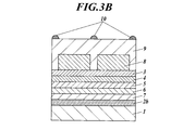
次に、電子注入層まで成膜した素子を真空のまま第1真空槽に戻した後、電子注入層の上にステンレス鋼製のマスクが配置されるように装置外部からリモートコントロールで設置した。このとき使用したマスクは1,000μm間隔で幅50μmのライン状の穴が空いている。次に、第2真空槽を4×10⁻⁴Paまで減圧した後、酸化モリブデン(6価)の入った加熱ボートに通電して加熱し、蒸着速度0.1~0.2nm/秒で上記マスク越しに成膜し、膜厚70nmの図2に模式図で示したようにパターニングされた透明保護層を設けた。上面図と側面から見た断面図で示した。 (Formation of transparent protective layer)
Next, after the element formed up to the electron injection layer was returned to the first vacuum chamber while being vacuumed, it was installed by remote control from the outside of the apparatus so that a stainless steel mask was placed on the electron injection layer. The mask used at this time has a line-shaped hole with a width of 50 μm at intervals of 1,000 μm. Next, after reducing the pressure in the second vacuum tank to 4 × 10 −4 Pa, the heating boat containing molybdenum oxide (hexavalent) was heated and heated, and the above was performed at a deposition rate of 0.1 to 0.2 nm / second. A transparent protective layer was formed over the mask and patterned as shown in the schematic diagram of FIG. Shown in top view and cross-sectional view from the side.
陰極上に、シャドーマスクを用いてスパッタ法で線幅50μm、厚み1μm、ピッチ1,000μmの間隔で図2のようなライン状の銀パターンから成る補助電極を透明保護層がパターニングされていない領域上に作製した。 (Preparation of auxiliary electrode)
An area where the transparent protective layer is not patterned on the cathode on the auxiliary electrode made of a line-shaped silver pattern as shown in FIG. 2 at intervals of a line width of 50 μm, a thickness of 1 μm, and a pitch of 1,000 μm using a shadow mask. Made above.
有機EL素子1-18と同様な方法で硬化・封止して、両面エミッション型有機EL素子1-24を得た。 (Element sealing)
It was cured and sealed in the same manner as the organic EL element 1-18 to obtain a double-sided emission type organic EL element 1-24.
透明保護層の材料を表1に記載の材料に変更した以外は有機EL素子1-24と同様な方法で、有機EL素子1-25~1-26を作製した。 [Production of Organic EL Elements 1-25 to 1-26]
Organic EL elements 1-25 to 1-26 were produced in the same manner as the organic EL element 1-24, except that the material of the transparent protective layer was changed to the material shown in Table 1.
上記作製した各有機EL素子について、下記の方法に従って電圧の測定を行った。 << Evaluation of organic EL elements >>
About each produced said organic EL element, the voltage was measured in accordance with the following method.
上記で作製した各有機EL素子に対し、陽極側と陰極側の両側の正面輝度の和が1000cd/m2となるときの電圧を各素子の電圧とした。なお、輝度の測定には分光放射輝度計CS-1000(コニカミノルタセンシング製)を用いた。得られた電圧の数値が小さいほど、好ましい結果であることを表す。 (Measurement of voltage)
With respect to each organic EL element produced as described above, the voltage when the sum of the front luminances on both the anode side and the cathode side was 1000 cd / m 2 was defined as the voltage of each element. For measurement of luminance, a spectral radiance meter CS-1000 (manufactured by Konica Minolta Sensing) was used. The smaller the numerical value of the voltage obtained, the better the result.
作製した有機EL素子に対し、2.5mA/cm2で定電流を印加したときの外部取り出し量子効率(%)を測定した。外部取り出し量子効率は以下の式により算出される。 (External quantum efficiency)
The external extraction quantum efficiency (%) when a constant current was applied to the produced organic EL element at 2.5 mA / cm 2 was measured. The external extraction quantum efficiency is calculated by the following equation.
なお、測定には分光放射輝度計CS-1000(コニカミノルタセンシング製)を用いた。有機EL素子1-1~1-26の外部取り出し量子効率は、有機EL素子1-1(比較例)の測定値を1.0とした相対値で表した。外部取り出し量子効率の相対値を表1に記した。 External extraction quantum efficiency (%) = number of photons emitted to the outside of the organic EL element / number of electrons sent to the organic EL element × 100
For the measurement, a spectral radiance meter CS-1000 (manufactured by Konica Minolta Sensing) was used. The external extraction quantum efficiencies of the organic EL elements 1-1 to 1-26 were expressed as relative values with the measured value of the organic EL element 1-1 (comparative example) being 1.0. The relative value of the external extraction quantum efficiency is shown in Table 1.

有機EL素子2-1~2-23は発光面積が5cm×5cmとなるように作製した。 << Production of top emission type organic EL elements >>
The organic EL elements 2-1 to 2-23 were fabricated so that the light emitting area was 5 cm × 5 cm.
(陰極の形成)
透明な基板1の上に厚さ100nmとなる条件でアルミニウムをスパッタ法で成膜、パターニングして、アルミニウム層から成る陽極を形成した。次いで、アルミニウム層を設けた基板を、イソプロピルアルコールで超音波洗浄し、乾燥窒素ガスで乾燥し、UVオゾン洗浄を5分間行った。 [Production of Organic EL Element 2-1]
(Formation of cathode)
Aluminum was formed on the
このアルミニウム層を設けた基板を市販の真空蒸着装置の基板ホルダーに固定し、タンタル製抵抗加熱ボートにフッ化カリウム、Alq3、BAlq、DPVBi、α-NPDをそれぞれ入れ、真空蒸着装置の第1真空槽に取り付けた。 (Electron injection layer to hole injection / hole transport formation)
The substrate provided with the aluminum layer is fixed to a substrate holder of a commercially available vacuum deposition apparatus, and potassium fluoride, Alq 3 , BAlq, DPVBi, and α-NPD are placed in a tantalum resistance heating boat, respectively. Attached to a vacuum chamber.
次に、正孔注入/正孔輸送層まで成膜した素子をあらかじめITOターゲットを装着した市販の平行平板スパッタリング装置に移し、スパッタリング装置のチャンバー内を5×10-3Paまで減圧した後、窒素ガスと酸素ガスを流しながら、DC出力500Wで放電し、成膜速度10nm/秒で膜厚100nmのITO導電層の透明導電性層(陽極)を形成した。 (Formation of transparent conductive layer (anode))
Next, the element formed up to the hole injection / hole transport layer was transferred to a commercially available parallel plate sputtering apparatus equipped with an ITO target in advance, and the pressure in the chamber of the sputtering apparatus was reduced to 5 × 10 −3 Pa, While flowing gas and oxygen gas, discharging was performed at a DC output of 500 W to form a transparent conductive layer (anode) of an ITO conductive layer having a film thickness of 10 nm / second and a film thickness of 100 nm.
最後に、上記で得られた素子をガラスケースで覆い、厚み300μmのガラス基板を封止用基板として用い、周囲にシール材としてエポキシ系光硬化型接着剤(東亞合成社製ラックストラックLC0629B)を適用し、これを前記透明支持基板と密着させ、ガラス基板側からUV光を照射して、硬化・封止して、トップエミッション型有機EL素子2-1を得た。 (Element sealing)
Finally, the device obtained above is covered with a glass case, a glass substrate having a thickness of 300 μm is used as a sealing substrate, and an epoxy-based photocurable adhesive (Lux Track LC0629B, manufactured by Toagosei Co., Ltd.) is used as a sealing material around it. This was applied, brought into close contact with the transparent support substrate, irradiated with UV light from the glass substrate side, cured and sealed to obtain a top emission type organic EL device 2-1.
(陰極~正孔注入/正孔輸送層の形成)
陰極~正孔注入/正孔輸送層までは有機EL素子2-1と同様な方法で成膜した。 [Production of Organic EL Element 2-2]
(Cathode to hole injection / hole transport layer formation)
The layers from the cathode to the hole injection / hole transport layer were formed in the same manner as in the organic EL device 2-1.
次に、正孔注入/正孔輸送層まで成膜した素子を真空のまま第1真空槽に戻し、第1真空槽を4×10-4Paまで減圧した後、酸化カルシウムの入った加熱ボートに通電して加熱し、酸素ガスを導入せずに、蒸着速度0.1~0.2nm/秒で蒸着を行って膜厚20nmの透明保護層を設けた。 (Formation of transparent protective layer)
Next, the element formed up to the hole injection / hole transport layer was returned to the first vacuum chamber in a vacuum state, the first vacuum chamber was depressurized to 4 × 10 −4 Pa, and then a heated boat containing calcium oxide A transparent protective layer having a film thickness of 20 nm was formed by conducting vapor deposition at a vapor deposition rate of 0.1 to 0.2 nm / second without introducing oxygen gas and heating.
有機EL素子2-1と同様にして陰極を成膜した。 (Formation of anode)
A cathode was formed in the same manner as in the organic EL element 2-1.
有機EL素子2-1と同様な方法で硬化・封止して、トップエミッション型有機EL素子2-2を得た。 (Element sealing)
Curing and sealing were performed in the same manner as for the organic EL element 2-1, to obtain a top emission type organic EL element 2-2.
透明保護層の膜厚を20nmから70nmに変更した以外は有機EL素子2-2と同様な方法でトップエミッション型有機EL素子2-3を得た。 [Preparation of organic EL element 2-3]
A top emission type organic EL device 2-3 was obtained in the same manner as the organic EL device 2-2 except that the thickness of the transparent protective layer was changed from 20 nm to 70 nm.
透明保護層の材料を酸化カルシウムから酸化ランタンに変更した以外は有機EL素子2-2と同様な方法でトップエミッション型有機EL素子2-4を得た。 [Preparation of organic EL element 2-4]
A top emission type organic EL element 2-4 was obtained in the same manner as the organic EL element 2-2 except that the material of the transparent protective layer was changed from calcium oxide to lanthanum oxide.
透明保護層の膜厚を20nmから70nmに変更した以外は有機EL素子2-4と同様な方法でトップエミッション型有機EL素子2-5を得た。 [Preparation of organic EL element 2-5]
A top emission type organic EL element 2-5 was obtained in the same manner as the organic EL element 2-4 except that the thickness of the transparent protective layer was changed from 20 nm to 70 nm.
(陰極の形成)
有機EL素子2-1と同様な方法でアルミニウム層から成る陰極を形成した。 [Preparation of organic EL element 2-6]
(Formation of cathode)
A cathode composed of an aluminum layer was formed in the same manner as in the organic EL element 2-1.
このアルミニウム層を設けた基板を市販の真空蒸着装置の基板ホルダーに固定し、タンタル製抵抗加熱ボートにフッ化カリウム、Alq3、BAlq、H4、Ir-4、α-NPDをそれぞれ入れ、真空蒸着装置の第1真空槽に取り付けた。 (Electron injection layer to hole injection / hole transport formation)
The substrate provided with the aluminum layer is fixed to a substrate holder of a commercially available vacuum deposition apparatus, and potassium fluoride, Alq 3 , BAlq, H4, Ir-4, α-NPD are placed in a tantalum resistance heating boat, respectively, and vacuum deposition is performed. Attached to the first vacuum chamber of the apparatus.
次に、正孔注入/正孔輸送層まで成膜した素子を真空のまま第1真空槽に戻し、第1真空槽を4×10-4Paまで減圧した後、酸化バナジウムの入った加熱ボートに通電して加熱し、蒸着速度0.1~0.2nm/秒で蒸着を行って膜厚20nmの透明保護層を設けた。 (Formation of transparent protective layer)
Next, the element formed up to the hole injection / hole transport layer was returned to the first vacuum chamber while being vacuumed, and the first vacuum chamber was decompressed to 4 × 10 −4 Pa, and then a heating boat containing vanadium oxide. The film was heated by applying current to the film, and was deposited at a deposition rate of 0.1 to 0.2 nm / second to provide a 20 nm thick transparent protective layer.
次に、透明保護層まで成膜した素子をあらかじめITOターゲットを装着した市販の平行平板スパッタリング装置に移し、スパッタリング装置のチャンバー内を5×10⁻³Paまで減圧した後、窒素ガスと酸素ガスを流しながら、DC出力500Wで放電し、成膜速度10nm/秒で膜厚100nmのITO導電層の透明導電性層(陽極)を形成した。 (Formation of transparent conductive layer (anode))
Next, the element formed up to the transparent protective layer is transferred to a commercially available parallel plate sputtering apparatus equipped with an ITO target in advance, and the pressure in the chamber of the sputtering apparatus is reduced to 5 × 10 −3 Pa, and then nitrogen gas and oxygen gas are added. While flowing, it was discharged at a DC output of 500 W to form a transparent conductive layer (anode) of an ITO conductive layer having a film thickness of 10 nm / second and a film thickness of 100 nm.
有機EL素子2-1と同様な方法で硬化・封止して、トップエミッション型有機EL素子2-6を得た。 (Element sealing)
Curing and sealing were performed in the same manner as for the organic EL element 2-1, to obtain a top emission type organic EL element 2-6.
(陰極~正孔注入/正孔輸送層の形成)
陰極~正孔注入/正孔輸送層までは有機EL素子2-6と同様な方法で成膜した。 [Preparation of organic EL element 2-7]
(Cathode to hole injection / hole transport layer formation)
The layers from the cathode to the hole injection / hole transport layer were formed in the same manner as in the organic EL element 2-6.
次に、電子注入層まで成膜した素子を真空のまま第1真空槽に戻し、第1真空槽を4×10⁻⁴Paまで減圧した後、酸化モリブデン(6価)の入った加熱ボートに通電して加熱し、蒸着速度0.1~0.2nm/秒で膜厚20nmの透明保護層を設けた。 (Formation of transparent protective layer)
Next, the element formed up to the electron injection layer was returned to the first vacuum chamber while being vacuumed, and the first vacuum chamber was decompressed to 4 × 10 −4 Pa, and then placed on a heating boat containing molybdenum oxide (hexavalent). A transparent protective layer having a film thickness of 20 nm was provided at a deposition rate of 0.1 to 0.2 nm / sec.
有機EL素子2-6と同様にして陽極を成膜した。 (Formation of anode)
An anode was formed in the same manner as in the organic EL element 2-6.
有機EL素子2-6と同様な方法で硬化・封止して、トップエミッション型有機EL素子2-7を得た。なお、同様な方法で作製した素子を別途作製し、透明保護層をESCAで分析し、透明保護層を構成している酸化モリブデン(6価)は酸素欠陥状態になっていることを確認した。 (Element sealing)
Curing and sealing were performed in the same manner as for organic EL element 2-6 to obtain top emission type organic EL element 2-7. In addition, the element produced by the same method was produced separately, the transparent protective layer was analyzed by ESCA, and it was confirmed that molybdenum oxide (hexavalent) constituting the transparent protective layer was in an oxygen defect state.
透明保護層の膜厚を表2に記載の値に変更した以外は有機EL素子2-7と同様な方法で、有機EL素子2-8~2-12を作製した。 [Production of organic EL elements 2-8 to 2-12]
Organic EL elements 2-8 to 2-12 were produced in the same manner as the organic EL element 2-7, except that the thickness of the transparent protective layer was changed to the values shown in Table 2.
リン光発光性化合物を表2に記載の化合物に変更した以外は有機EL素子2-9と同様な方法で、有機EL素子2-13~2-15を作製した。 [Production of organic EL elements 2-13 to 2-15]
Organic EL devices 2-13 to 2-15 were produced in the same manner as the organic EL device 2-9, except that the phosphorescent compound was changed to the compounds shown in Table 2.
透明保護層の材料を表2に記載の材料に変更した以外は有機EL素子2-15と同様な方法で、有機EL素子2-16~2-17を作製した。なお、表2に記した酸化モリブデンは6価であり、酸化レニウムは6価であり、酸化ニッケルは2価である。 [Production of organic EL elements 2-16 to 2-17]
Organic EL elements 2-16 to 2-17 were produced in the same manner as the organic EL element 2-15, except that the material of the transparent protective layer was changed to the material shown in Table 2. Note that molybdenum oxide shown in Table 2 is hexavalent, rhenium oxide is hexavalent, and nickel oxide is divalent.
(陽極~陰極の形成)
陰極~陽極までは有機EL素子2-15と同様な方法で成膜した。 [Preparation of organic EL element 2-18]
(Formation of anode to cathode)
A film was formed from the cathode to the anode in the same manner as in the organic EL element 2-15.
陽極上に、シャドーマスクを用いてスパッタ法で線幅50μm、厚み1μm、ピッチ1,000μmの間隔でライン状の銀パターンから成る補助電極を作製した。 (Preparation of auxiliary electrode)
On the anode, an auxiliary electrode composed of a line-shaped silver pattern was produced by a sputtering method using a shadow mask at a line width of 50 μm, a thickness of 1 μm, and a pitch of 1,000 μm.
有機EL素子2-15と同様な方法で硬化・封止して、トップエミッション型有機EL素子2-18を得た。 (Element sealing)
Curing and sealing were performed in the same manner as for the organic EL element 2-15 to obtain a top emission type organic EL element 2-18.
透明保護層の材料を表2に記載の材料に変更した以外は有機EL素子2-15と同様な方法で、有機EL素子2-19~2-20を作製した。 [Preparation of organic EL elements 2-19 to 2-20]
Organic EL elements 2-19 to 2-20 were produced in the same manner as the organic EL element 2-15 except that the material of the transparent protective layer was changed to the material shown in Table 2.
(陰極~正孔注入/正孔輸送層の形成)
陰極~正孔注入/正孔輸送層までは有機EL素子2-18と同様な方法で成膜した。 [Production of organic EL element 2-21]
(Cathode to hole injection / hole transport layer formation)
The layers from the cathode to the hole injection / hole transport layer were formed in the same manner as in the organic EL device 2-18.
次に、正孔注入/正孔輸送層まで成膜した素子を真空のまま第1真空槽に戻した後、電子注入層の上にステンレス鋼製のマスクが配置されるように装置外部からリモートコントロールで設置した。このとき使用したマスクは1,000μm間隔で幅50μmのライン状の穴が空いている。次に、第2真空槽を4×10-4Paまで減圧した後、酸化モリブデン(6価)の入った加熱ボートに通電して加熱し、蒸着速度0.1~0.2nm/秒で上記マスク越しに成膜し、膜厚70nmの図3のようにパターニングされた透明保護層を設けた。図3に、上面図及び側面から見た断面図を示した。 (Formation of transparent protective layer)
Next, after the element formed up to the hole injection / hole transport layer is returned to the first vacuum chamber in a vacuum state, the device is remotely controlled from the outside so that a stainless steel mask is disposed on the electron injection layer. Installed with control. The mask used at this time has a line-shaped hole with a width of 50 μm at intervals of 1,000 μm. Next, after reducing the pressure in the second vacuum tank to 4 × 10 −4 Pa, the heating boat containing molybdenum oxide (hexavalent) was energized and heated, and the above was performed at a deposition rate of 0.1 to 0.2 nm / second. A transparent protective layer was formed over the mask and patterned as shown in FIG. FIG. 3 shows a top view and a cross-sectional view seen from the side.
陰極上に、シャドーマスクを用いてスパッタ法で線幅50μm、厚み1μm、ピッチ1,000μmの間隔で図3のようなライン状の銀パターンから成る補助電極を透明保護層がパターニングされていない領域上に作製した。 (Preparation of auxiliary electrode)
An area where the transparent protective layer is not patterned on the cathode, with an auxiliary electrode made of a linear silver pattern as shown in FIG. 3 at intervals of 50 μm in line width, 1 μm in thickness and 1,000 μm in pitch using a shadow mask. Made above.
有機EL素子2-15と同様な方法で硬化・封止して、トップエミッション型有機EL素子2-21を得た。 (Element sealing)
It was cured and sealed in the same manner as the organic EL element 2-15 to obtain a top emission type organic EL element 2-21.
透明保護層の材料を表2に記載の材料に変更した以外は有機EL素子2-21と同様な方法で、有機EL素子2-22~2-23を作製した。 [Production of organic EL elements 2-22 to 2-23]
Organic EL elements 2-22 to 2-23 were produced in the same manner as the organic EL element 2-21 except that the material of the transparent protective layer was changed to the material shown in Table 2.
上記作製した各有機EL素子について、下記の方法に従って電圧の測定を行った。 << Evaluation of organic EL elements >>
About each produced said organic EL element, the voltage was measured in accordance with the following method.
上記で作製した各有機EL素子に対し、陽極側の正面輝度が1000cd/m2となるときの電圧を各素子の電圧とした。なお、輝度の測定には分光放射輝度計CS-1000(コニカミノルタセンシング製)を用いた。得られた電圧の数値が小さいほど、好ましい結果であることを表す。 (Measurement of voltage)
For each organic EL element produced above, the voltage when the front luminance on the anode side was 1000 cd / m 2 was taken as the voltage of each element. For measurement of luminance, a spectral radiance meter CS-1000 (manufactured by Konica Minolta Sensing) was used. The smaller the numerical value of the voltage obtained, the better the result.
作製した有機EL素子に対し、2.5mA/cm2で定電流を印加したときの外部取り出し量子効率(%)を測定した。外部取り出し量子効率は以下の式により算出される。 (External quantum efficiency)
The external extraction quantum efficiency (%) when a constant current was applied to the produced organic EL element at 2.5 mA / cm 2 was measured. The external extraction quantum efficiency is calculated by the following equation.
なお、測定には分光放射輝度計CS-1000(コニカミノルタセンシング製)を用いた。有機EL素子2-1~2-23の外部取り出し量子効率は、有機EL素子2-1(比較例)の測定値を1.0とした相対値で表した。外部取り出し量子効率の相対値を表2に記した。 External extraction quantum efficiency (%) = number of photons emitted to the outside of the organic EL element / number of electrons sent to the organic EL element × 100
For the measurement, a spectral radiance meter CS-1000 (manufactured by Konica Minolta Sensing) was used. The external extraction quantum efficiencies of the organic EL elements 2-1 to 2-23 were expressed as relative values with the measured value of the organic EL element 2-1 (comparative example) being 1.0. Table 2 shows the relative values of the external extraction quantum efficiency.

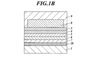
2a 陽極
2b 陰極
3 正孔注入層
4 正孔輸送層
5 発光層
6 電子輸送層
7 電子注入層
8 透明保護層
9 透明導電性層
10 補助電極 DESCRIPTION OF
Claims (14)
- 少なくとも発光層及び透明導電性層を有する有機エレクトロルミネッセンス素子において、該発光層と該透明導電性層との間に透明保護層が配置されており、該発光層はリン光発光性化合物を含有し、かつ該透明保護層が金属酸化物を含有し、該金属酸化物がモリブデン酸化物(6価)、レニウム酸化物(6価)又はニッケル酸化物(2価)であり、該モリブデン酸化物(6価)、レニウム酸化物(6価)及びニッケル酸化物(2価)は酸素欠損状態であることを特徴とする有機エレクトロルミネッセンス素子。 In an organic electroluminescence device having at least a light emitting layer and a transparent conductive layer, a transparent protective layer is disposed between the light emitting layer and the transparent conductive layer, and the light emitting layer contains a phosphorescent compound. And the transparent protective layer contains a metal oxide, and the metal oxide is molybdenum oxide (hexavalent), rhenium oxide (hexavalent) or nickel oxide (divalent). Hexavalent), rhenium oxide (hexavalent), and nickel oxide (divalent) are in an oxygen deficient state.
- 前記透明保護層の膜厚が60nm以上、150nm以下であることを特徴とする請求項1に記載の有機エレクトロルミネッセンス素子。 The organic electroluminescent element according to claim 1, wherein the transparent protective layer has a thickness of 60 nm or more and 150 nm or less.
- 前記発光層と前記透明保護層との間に電子輸送層を有することを特徴とする請求項1又は2に記載の有機エレクトロルミネッセンス素子。 3. The organic electroluminescence device according to claim 1, further comprising an electron transport layer between the light emitting layer and the transparent protective layer.
- 前記発光層と前記透明保護層との間に正孔輸送層を有することを特徴とする請求項1又は2に記載の有機エレクトロルミネッセンス素子。 3. The organic electroluminescence device according to claim 1, further comprising a hole transport layer between the light emitting layer and the transparent protective layer.
- 前記電子輸送層が下記一般式(1)で表される化合物を含有することを特徴とする請求項3に記載の有機エレクトロルミネッセンス素子。
一般式(1) (Ar1)n1-Y1
〔式中、n1は1以上の整数を表し、Y1はn1が1の場合は置換基を表し、n1が2以上の場合は単なる結合手又はn1価の連結基を表す。Ar1は下記一般式(A)で表される基を表し、n1が2以上の場合、複数のAr1は同一でも異なっていてもよい。但し、前記一般式(1)で表される化合物は分子内に3環以上の環が縮合してなる縮合芳香族複素環を少なくとも2つ有する。〕

Formula (1) (Ar1) n1 -Y1
[Wherein, n1 represents an integer of 1 or more, Y1 represents a substituent when n1 is 1, and represents a single bond or an n1-valent linking group when n1 is 2 or more. Ar1 represents a group represented by the following general formula (A). When n1 is 2 or more, a plurality of Ar1s may be the same or different. However, the compound represented by the general formula (1) has at least two condensed aromatic heterocycles in which three or more rings are condensed in the molecule. ]
- 前記一般式(1)で表される化合物が、下記一般式(2)で表される化合物であることを特徴とする請求項5に記載の有機エレクトロルミネッセンス素子。

- 前記一般式(2)で表される化合物が、下記一般式(3)で表される化合物であることを特徴とする請求項6に記載の有機エレクトロルミネッセンス素子。

- 前記リン光発光性化合物が下記一般式(4)で表されることを特徴とする請求項1~7のいずれか一項に記載の有機エレクトロルミネッセンス素子。

- 前記一般式(4)で表される化合物が下記一般式(5)で表される化合物であることを特徴とする請求項8に記載の有機エレクトロルミネッセンス素子。

- 前記M1がイリジウムを表すことを特徴とする請求項8又は9に記載の有機エレクトロルミネッセンス素子。 The organic electroluminescence device according to claim 8 or 9, wherein M1 represents iridium.
- 前記透明導電性層上に補助電極を有することを特徴とする請求項1~10のいずれか一項に記載の有機エレクトロルミネッセンス素子。 11. The organic electroluminescence device according to claim 1, further comprising an auxiliary electrode on the transparent conductive layer.
- 前記透明保護層がパターニングされており、かつ前記補助電極が透明保護層のパターニングされていない領域上に形成されていることを特徴とする請求項11に記載の有機エレクトロルミネッセンス素子。 The organic electroluminescence device according to claim 11, wherein the transparent protective layer is patterned, and the auxiliary electrode is formed on an unpatterned region of the transparent protective layer.
- 両面エミッション型であることを特徴とする請求項1~12のいずれか一項に記載の有機エレクトロルミネッセンス素子。 The organic electroluminescence device according to any one of claims 1 to 12, which is a double-sided emission type.
- 請求項1~13のいずれか一項に記載の有機エレクトロルミネッセンス素子を備えたことを特徴とする照明装置。 An illumination device comprising the organic electroluminescence element according to any one of claims 1 to 13.
Priority Applications (4)
| Application Number | Priority Date | Filing Date | Title |
|---|---|---|---|
| JP2012557888A JP5817742B2 (en) | 2011-02-15 | 2012-02-06 | ORGANIC ELECTROLUMINESCENT ELEMENT AND LIGHTING DEVICE |
| US13/984,713 US9368735B2 (en) | 2011-02-15 | 2012-02-06 | Organic electroluminescence element and illumination device |
| EP12746825.4A EP2677560A4 (en) | 2011-02-15 | 2012-02-06 | Organic electroluminescence element and illumination device |
| US15/152,068 US9871222B2 (en) | 2011-02-15 | 2016-05-11 | Organic electroluminescence element and illumination device |
Applications Claiming Priority (2)
| Application Number | Priority Date | Filing Date | Title |
|---|---|---|---|
| JP2011-029460 | 2011-02-15 | ||
| JP2011029460 | 2011-02-15 |
Related Child Applications (2)
| Application Number | Title | Priority Date | Filing Date |
|---|---|---|---|
| US13/984,713 A-371-Of-International US9368735B2 (en) | 2011-02-15 | 2012-02-06 | Organic electroluminescence element and illumination device |
| US15/152,068 Division US9871222B2 (en) | 2011-02-15 | 2016-05-11 | Organic electroluminescence element and illumination device |
Publications (1)
| Publication Number | Publication Date |
|---|---|
| WO2012111462A1 true WO2012111462A1 (en) | 2012-08-23 |
Family
ID=46672390
Family Applications (1)
| Application Number | Title | Priority Date | Filing Date |
|---|---|---|---|
| PCT/JP2012/052584 WO2012111462A1 (en) | 2011-02-15 | 2012-02-06 | Organic electroluminescence element and illumination device |
Country Status (4)
| Country | Link |
|---|---|
| US (2) | US9368735B2 (en) |
| EP (1) | EP2677560A4 (en) |
| JP (1) | JP5817742B2 (en) |
| WO (1) | WO2012111462A1 (en) |
Cited By (37)
| Publication number | Priority date | Publication date | Assignee | Title |
|---|---|---|---|---|
| WO2014042163A1 (en) * | 2012-09-12 | 2014-03-20 | 出光興産株式会社 | Novel compound, material for organic electroluminescence element, organic electroluminescence element, and electronic device |
| WO2014147134A1 (en) | 2013-03-20 | 2014-09-25 | Basf Se | Azabenzimidazole carbene complexes as efficiency booster in oleds |
| WO2014177518A1 (en) | 2013-04-29 | 2014-11-06 | Basf Se | Transition metal complexes with carbene ligands and the use thereof in oleds |
| WO2015000955A1 (en) | 2013-07-02 | 2015-01-08 | Basf Se | Monosubstituted diazabenzimidazole carbene metal complexes for use in organic light emitting diodes |
| WO2015063046A1 (en) | 2013-10-31 | 2015-05-07 | Basf Se | Azadibenzothiophenes for electronic applications |
| WO2016016791A1 (en) | 2014-07-28 | 2016-02-04 | Idemitsu Kosan Co., Ltd (Ikc) | 2,9-functionalized benzimidazolo[1,2-a]benzimidazoles as hosts for organic light emitting diodes (oleds) |
| EP2982676A1 (en) | 2014-08-07 | 2016-02-10 | Idemitsu Kosan Co., Ltd. | Benzimidazo[2,1-B]benzoxazoles for electronic applications |
| EP2993215A1 (en) | 2014-09-04 | 2016-03-09 | Idemitsu Kosan Co., Ltd. | Azabenzimidazo[2,1-a]benzimidazoles for electronic applications |
| EP3015469A1 (en) | 2014-10-30 | 2016-05-04 | Idemitsu Kosan Co., Ltd. | 5-((benz)imidazol-2-yl)benzimidazo[1,2-a]benzimidazoles for electronic applications |
| WO2016079169A1 (en) | 2014-11-18 | 2016-05-26 | Basf Se | Pt- or pd-carbene complexes for use in organic light emitting diodes |
| WO2016079667A1 (en) | 2014-11-17 | 2016-05-26 | Idemitsu Kosan Co., Ltd. | Indole derivatives for electronic applications |
| EP3034506A1 (en) | 2014-12-15 | 2016-06-22 | Idemitsu Kosan Co., Ltd | 4-functionalized carbazole derivatives for electronic applications |
| EP3034507A1 (en) | 2014-12-15 | 2016-06-22 | Idemitsu Kosan Co., Ltd | 1-functionalized dibenzofurans and dibenzothiophenes for organic light emitting diodes (OLEDs) |
| EP3053918A1 (en) | 2015-02-06 | 2016-08-10 | Idemitsu Kosan Co., Ltd | 2-carbazole substituted benzimidazoles for electronic applications |
| EP3054498A1 (en) | 2015-02-06 | 2016-08-10 | Idemitsu Kosan Co., Ltd. | Bisimidazodiazocines |
| EP3061759A1 (en) | 2015-02-24 | 2016-08-31 | Idemitsu Kosan Co., Ltd | Nitrile substituted dibenzofurans |
| EP3070144A1 (en) | 2015-03-17 | 2016-09-21 | Idemitsu Kosan Co., Ltd. | Seven-membered ring compounds |
| EP3072943A1 (en) | 2015-03-26 | 2016-09-28 | Idemitsu Kosan Co., Ltd. | Dibenzofuran/carbazole-substituted benzonitriles |
| EP3075737A1 (en) | 2015-03-31 | 2016-10-05 | Idemitsu Kosan Co., Ltd | Benzimidazolo[1,2-a]benzimidazole carrying aryl- or heteroarylnitril groups for organic light emitting diodes |
| WO2016193243A1 (en) | 2015-06-03 | 2016-12-08 | Udc Ireland Limited | Highly efficient oled devices with very short decay times |
| EP3150604A1 (en) | 2015-10-01 | 2017-04-05 | Idemitsu Kosan Co., Ltd. | Benzimidazolo[1,2-a]benzimidazole carrying benzimidazolo[1,2-a]benzimidazolyl groups, carbazolyl groups, benzofurane groups or benzothiophene groups for organic light emitting diodes |
| EP3150606A1 (en) | 2015-10-01 | 2017-04-05 | Idemitsu Kosan Co., Ltd. | Benzimidazolo[1,2-a]benzimidazoles carrying benzofurane or benzothiophene groups for organic light emitting diodes |
| WO2017056053A1 (en) | 2015-10-01 | 2017-04-06 | Idemitsu Kosan Co., Ltd. | Benzimidazolo[1,2-a]benzimidazole carrying benzimidazolo[1,2-a]benzimidazolyl groups, carbazolyl groups, benzofurane groups or benzothiophene groups for organic light emitting diodes |
| WO2017056055A1 (en) | 2015-10-01 | 2017-04-06 | Idemitsu Kosan Co., Ltd. | Benzimidazolo[1,2-a]benzimidazole carrying triazine groups for organic light emitting diodes |
| WO2017078182A1 (en) | 2015-11-04 | 2017-05-11 | Idemitsu Kosan Co., Ltd. | Benzimidazole fused heteroaryls |
| WO2017093958A1 (en) | 2015-12-04 | 2017-06-08 | Idemitsu Kosan Co., Ltd. | Benzimidazolo[1,2-a]benzimidazole derivatives for organic light emitting diodes |
| EP3184534A1 (en) | 2015-12-21 | 2017-06-28 | UDC Ireland Limited | Transition metal complexes with tripodal ligands and the use thereof in oleds |
| WO2017109727A1 (en) | 2015-12-21 | 2017-06-29 | Idemitsu Kosan Co., Ltd. | Hetero-condensed phenylquinazolines and their use in electronic devices |
| WO2017178864A1 (en) | 2016-04-12 | 2017-10-19 | Idemitsu Kosan Co., Ltd. | Seven-membered ring compounds |
| EP3239161A1 (en) | 2013-07-31 | 2017-11-01 | UDC Ireland Limited | Luminescent diazabenzimidazole carbene metal complexes |
| TWI612043B (en) * | 2012-09-07 | 2018-01-21 | 出光興產股份有限公司 | Novel aromatic heterocyclic derivative, material for organic electroluminescence device, material solution for organic electroluminescence device, and organic electroluminescence device |
| EP3318566A1 (en) | 2012-09-20 | 2018-05-09 | UDC Ireland Limited | Azadibenzofurans for electronic applications |
| EP3418285A1 (en) | 2017-06-20 | 2018-12-26 | Idemitsu Kosan Co., Ltd. | Composition comprising a substituted ir complex and a phenylquinazoline bridged with a heteroatom |
| EP3466954A1 (en) | 2017-10-04 | 2019-04-10 | Idemitsu Kosan Co., Ltd. | Fused phenylquinazolines bridged with a heteroatom |
| EP3466957A1 (en) | 2014-08-08 | 2019-04-10 | UDC Ireland Limited | Oled comprising an electroluminescent imidazo-quinoxaline carbene metal complexes |
| US10347851B2 (en) | 2013-12-20 | 2019-07-09 | Udc Ireland Limited | Highly efficient OLED devices with very short decay times |
| KR20240014470A (en) | 2021-05-28 | 2024-02-01 | 가부시키가이샤 큐럭스 | Top emission organic electroluminescence device and its design method |
Families Citing this family (7)
| Publication number | Priority date | Publication date | Assignee | Title |
|---|---|---|---|---|
| JP5817742B2 (en) * | 2011-02-15 | 2015-11-18 | コニカミノルタ株式会社 | ORGANIC ELECTROLUMINESCENT ELEMENT AND LIGHTING DEVICE |
| KR102261235B1 (en) | 2011-11-22 | 2021-06-04 | 이데미쓰 고산 가부시키가이샤 | Aromatic heterocyclic derivative, material for organic electroluminescent element, and organic electroluminescent element |
| US9642212B1 (en) | 2015-06-11 | 2017-05-02 | Darkside Scientific, Llc | Electroluminescent system and process |
| KR102410031B1 (en) * | 2015-07-07 | 2022-06-20 | 삼성디스플레이 주식회사 | Organic light emitting diode, manufacturing method for the same, and organic light emitting display device having the organic light emitting diode |
| BR112019001759A2 (en) | 2016-07-28 | 2019-05-07 | Darkside Scientific, Inc | electroluminescent system and process |
| TWI660533B (en) * | 2017-09-15 | 2019-05-21 | Industrial Technology Research Institute | Light emitting device and transparent electrode thereof |
| US11121076B2 (en) * | 2019-06-27 | 2021-09-14 | Texas Instruments Incorporated | Semiconductor die with conversion coating |
Citations (57)
| Publication number | Priority date | Publication date | Assignee | Title |
|---|---|---|---|---|
| US5061569A (en) | 1990-07-26 | 1991-10-29 | Eastman Kodak Company | Electroluminescent device with organic electroluminescent medium |
| JPH04297076A (en) | 1991-01-31 | 1992-10-21 | Toshiba Corp | Organic el element |
| JPH04308688A (en) | 1991-04-08 | 1992-10-30 | Pioneer Electron Corp | Organic electroluminescence element |
| JPH06325871A (en) | 1993-05-18 | 1994-11-25 | Mitsubishi Kasei Corp | Organic electroluminescent element |
| JPH08288069A (en) | 1995-04-07 | 1996-11-01 | Sanyo Electric Co Ltd | Organic electroluminescent element |
| JPH0917574A (en) | 1995-04-27 | 1997-01-17 | Pioneer Electron Corp | Organic electroluminescence element |
| JPH0945479A (en) | 1995-07-27 | 1997-02-14 | Hewlett Packard Co <Hp> | Organic electroluminescence device and manufacture of organic electroluminescence device |
| JPH09260062A (en) | 1996-03-25 | 1997-10-03 | Tdk Corp | Organic electroluminescence element |
| JPH1074586A (en) | 1996-07-29 | 1998-03-17 | Eastman Kodak Co | Two layer electron injection electrode used in electroluminescence device |
| JPH10270172A (en) | 1997-01-27 | 1998-10-09 | Junji Kido | Organic electroluminescent element |
| JPH11204258A (en) | 1998-01-09 | 1999-07-30 | Sony Corp | Electroluminescence element and its manufacture |
| JPH11204359A (en) | 1998-01-14 | 1999-07-30 | Tokin Corp | Method and device for manufacturing dust core |
| JPH11251067A (en) | 1998-03-02 | 1999-09-17 | Junji Kido | Organic electroluminescence element |
| JP2000058265A (en) | 1998-07-28 | 2000-02-25 | Eastman Kodak Co | Organic luminescence element and its manufacture |
| JP2000068063A (en) | 1998-07-28 | 2000-03-03 | Eastman Kodak Co | Organic luminescent element and manufacture of the same |
| JP2000196140A (en) | 1998-12-28 | 2000-07-14 | Sharp Corp | Organic electroluminescence element and fabrication thereof |
| JP2001102175A (en) | 1999-09-29 | 2001-04-13 | Junji Kido | Organic electroluminescent device, organic electroluminescent device group and method of controlling its emission spectrum |
| JP2001257076A (en) | 2000-03-13 | 2001-09-21 | Tdk Corp | Organic el element |
| JP2001313179A (en) | 2000-05-01 | 2001-11-09 | Mitsubishi Chemicals Corp | Organic electroluminescent element |
| JP2001357977A (en) | 2000-06-12 | 2001-12-26 | Fuji Photo Film Co Ltd | Organic electroluminescent element |
| JP2002008860A (en) | 2000-04-18 | 2002-01-11 | Mitsubishi Chemicals Corp | Organic electroluminescenct element |
| JP2002015871A (en) | 2000-04-27 | 2002-01-18 | Toray Ind Inc | Luminescent element |
| JP2002043056A (en) | 2000-07-19 | 2002-02-08 | Canon Inc | Light-emitting element |
| JP2002075645A (en) | 2000-08-29 | 2002-03-15 | Semiconductor Energy Lab Co Ltd | Light-emitting device |
| JP2002105445A (en) | 2000-09-29 | 2002-04-10 | Fuji Photo Film Co Ltd | Organic light-emitting element material and organic light-emitting element using the same |
| JP2002141173A (en) | 2000-08-22 | 2002-05-17 | Semiconductor Energy Lab Co Ltd | Light emitting device |
| JP2002203683A (en) | 2000-10-30 | 2002-07-19 | Toyota Central Res & Dev Lab Inc | Organic electroluminescent element |
| JP2002231453A (en) | 2000-11-30 | 2002-08-16 | Mitsubishi Chemicals Corp | Organic electroluminescence element |
| JP2002234888A (en) | 2001-02-09 | 2002-08-23 | Mitsui Chemicals Inc | Amine compound and organic electroluminescent element containing the same compound |
| JP2002255934A (en) | 2000-12-25 | 2002-09-11 | Fuji Photo Film Co Ltd | New compound, its polymer, light emission element material using these substances and the light emission element |
| JP2002260861A (en) | 2001-01-02 | 2002-09-13 | Eastman Kodak Co | Organic light-emitting device |
| JP2002280183A (en) | 2000-12-28 | 2002-09-27 | Toshiba Corp | Organic el element and display unit |
| JP2002299060A (en) | 2001-03-30 | 2002-10-11 | Fuji Photo Film Co Ltd | Organic light-emitting element |
| JP2002305084A (en) | 2000-12-25 | 2002-10-18 | Fuji Photo Film Co Ltd | New indole derivative and light emitting element using it |
| JP2002305083A (en) | 2001-04-04 | 2002-10-18 | Mitsubishi Chemicals Corp | Organic electroluminescent element |
| JP2002302516A (en) | 2001-04-03 | 2002-10-18 | Fuji Photo Film Co Ltd | New polymer and light-emitting element using the same |
| JP2002308855A (en) | 2001-04-05 | 2002-10-23 | Fuji Photo Film Co Ltd | New compound and luminescent element using the same |
| JP2002308837A (en) | 2001-04-05 | 2002-10-23 | Fuji Photo Film Co Ltd | New compound and light-emitting device using the same |
| JP2002319491A (en) | 2000-08-24 | 2002-10-31 | Fuji Photo Film Co Ltd | Light-emitting element and novel polymer organic electroluminescent element |
| JP2002334788A (en) | 2001-03-09 | 2002-11-22 | Sony Corp | Organic electroluminescent element |
| JP2002334786A (en) | 2001-03-09 | 2002-11-22 | Sony Corp | Organic electroluminescent element |
| JP2002334787A (en) | 2001-03-09 | 2002-11-22 | Sony Corp | Organic electroluminescent element |
| JP2002334789A (en) | 2001-03-09 | 2002-11-22 | Sony Corp | Organic electroluminescent element |
| JP2002338579A (en) | 2001-03-16 | 2002-11-27 | Fuji Photo Film Co Ltd | Heterocyclic compound and light emission element using the same |
| JP2002343568A (en) | 2001-05-10 | 2002-11-29 | Sony Corp | Organic electroluminescent element |
| JP2002352957A (en) | 2001-05-23 | 2002-12-06 | Honda Motor Co Ltd | Organic electoluminescence element |
| JP2002363227A (en) | 2001-04-03 | 2002-12-18 | Fuji Photo Film Co Ltd | New polymer and luminescent element using the same |
| JP2003003165A (en) | 2001-06-25 | 2003-01-08 | Showa Denko Kk | Organic luminescent element and luminescent material |
| JP2003027048A (en) | 2001-07-11 | 2003-01-29 | Fuji Photo Film Co Ltd | Luminescent element |
| JP2005135706A (en) * | 2003-10-29 | 2005-05-26 | Fuji Electric Holdings Co Ltd | Method for manufacturing organic el element |
| JP2005158693A (en) * | 2003-11-21 | 2005-06-16 | Samsung Sdi Co Ltd | Organic electroluminescent element |
| JP2005158583A (en) * | 2003-11-27 | 2005-06-16 | Seiko Epson Corp | Organic electroluminescent device and electronic equipment |
| JP2008041692A (en) * | 2006-08-01 | 2008-02-21 | Matsushita Electric Ind Co Ltd | Organic electroluminescent device and manufacturing method thereof |
| JP2009212222A (en) * | 2008-03-03 | 2009-09-17 | Panasonic Corp | Organic electroluminescent element |
| JP2010251675A (en) * | 2008-05-13 | 2010-11-04 | Konica Minolta Holdings Inc | Organic electroluminescent element, display device, and lighting device |
| JP2011009517A (en) * | 2009-06-26 | 2011-01-13 | Konica Minolta Holdings Inc | Organic electroluminescent element |
| WO2011040193A1 (en) * | 2009-09-30 | 2011-04-07 | 株式会社アルバック | Organic el and method for formation of electrode for organic el |
Family Cites Families (5)
| Publication number | Priority date | Publication date | Assignee | Title |
|---|---|---|---|---|
| JP4939284B2 (en) * | 2007-04-05 | 2012-05-23 | 財団法人山形県産業技術振興機構 | Organic electroluminescent device |
| DE102007024152A1 (en) * | 2007-04-18 | 2008-10-23 | Osram Opto Semiconductors Gmbh | Organic optoelectronic component |
| KR20100114052A (en) * | 2007-12-27 | 2010-10-22 | 이 아이 듀폰 디 네모아 앤드 캄파니 | Buffer bilayers for electronic devices |
| JP5531843B2 (en) * | 2009-07-31 | 2014-06-25 | 大日本印刷株式会社 | Device material for hole injection transport layer, ink for forming hole injection transport layer, device having hole injection transport layer, and method for producing the same |
| JP5817742B2 (en) * | 2011-02-15 | 2015-11-18 | コニカミノルタ株式会社 | ORGANIC ELECTROLUMINESCENT ELEMENT AND LIGHTING DEVICE |
-
2012
- 2012-02-06 JP JP2012557888A patent/JP5817742B2/en not_active Expired - Fee Related
- 2012-02-06 WO PCT/JP2012/052584 patent/WO2012111462A1/en active Application Filing
- 2012-02-06 EP EP12746825.4A patent/EP2677560A4/en not_active Withdrawn
- 2012-02-06 US US13/984,713 patent/US9368735B2/en not_active Expired - Fee Related
-
2016
- 2016-05-11 US US15/152,068 patent/US9871222B2/en active Active
Patent Citations (58)
| Publication number | Priority date | Publication date | Assignee | Title |
|---|---|---|---|---|
| US5061569A (en) | 1990-07-26 | 1991-10-29 | Eastman Kodak Company | Electroluminescent device with organic electroluminescent medium |
| JPH04297076A (en) | 1991-01-31 | 1992-10-21 | Toshiba Corp | Organic el element |
| JPH04308688A (en) | 1991-04-08 | 1992-10-30 | Pioneer Electron Corp | Organic electroluminescence element |
| JPH06325871A (en) | 1993-05-18 | 1994-11-25 | Mitsubishi Kasei Corp | Organic electroluminescent element |
| JPH08288069A (en) | 1995-04-07 | 1996-11-01 | Sanyo Electric Co Ltd | Organic electroluminescent element |
| JPH0917574A (en) | 1995-04-27 | 1997-01-17 | Pioneer Electron Corp | Organic electroluminescence element |
| JPH0945479A (en) | 1995-07-27 | 1997-02-14 | Hewlett Packard Co <Hp> | Organic electroluminescence device and manufacture of organic electroluminescence device |
| JPH09260062A (en) | 1996-03-25 | 1997-10-03 | Tdk Corp | Organic electroluminescence element |
| JPH1074586A (en) | 1996-07-29 | 1998-03-17 | Eastman Kodak Co | Two layer electron injection electrode used in electroluminescence device |
| JPH10270172A (en) | 1997-01-27 | 1998-10-09 | Junji Kido | Organic electroluminescent element |
| JPH11204258A (en) | 1998-01-09 | 1999-07-30 | Sony Corp | Electroluminescence element and its manufacture |
| JPH11204359A (en) | 1998-01-14 | 1999-07-30 | Tokin Corp | Method and device for manufacturing dust core |
| JPH11251067A (en) | 1998-03-02 | 1999-09-17 | Junji Kido | Organic electroluminescence element |
| JP2000068063A (en) | 1998-07-28 | 2000-03-03 | Eastman Kodak Co | Organic luminescent element and manufacture of the same |
| JP2000058265A (en) | 1998-07-28 | 2000-02-25 | Eastman Kodak Co | Organic luminescence element and its manufacture |
| JP2000196140A (en) | 1998-12-28 | 2000-07-14 | Sharp Corp | Organic electroluminescence element and fabrication thereof |
| JP2001102175A (en) | 1999-09-29 | 2001-04-13 | Junji Kido | Organic electroluminescent device, organic electroluminescent device group and method of controlling its emission spectrum |
| JP2001257076A (en) | 2000-03-13 | 2001-09-21 | Tdk Corp | Organic el element |
| JP2002008860A (en) | 2000-04-18 | 2002-01-11 | Mitsubishi Chemicals Corp | Organic electroluminescenct element |
| JP2002015871A (en) | 2000-04-27 | 2002-01-18 | Toray Ind Inc | Luminescent element |
| JP2001313179A (en) | 2000-05-01 | 2001-11-09 | Mitsubishi Chemicals Corp | Organic electroluminescent element |
| JP2001357977A (en) | 2000-06-12 | 2001-12-26 | Fuji Photo Film Co Ltd | Organic electroluminescent element |
| JP2002043056A (en) | 2000-07-19 | 2002-02-08 | Canon Inc | Light-emitting element |
| JP2002141173A (en) | 2000-08-22 | 2002-05-17 | Semiconductor Energy Lab Co Ltd | Light emitting device |
| JP2002319491A (en) | 2000-08-24 | 2002-10-31 | Fuji Photo Film Co Ltd | Light-emitting element and novel polymer organic electroluminescent element |
| JP2002075645A (en) | 2000-08-29 | 2002-03-15 | Semiconductor Energy Lab Co Ltd | Light-emitting device |
| JP2002105445A (en) | 2000-09-29 | 2002-04-10 | Fuji Photo Film Co Ltd | Organic light-emitting element material and organic light-emitting element using the same |
| JP2002203683A (en) | 2000-10-30 | 2002-07-19 | Toyota Central Res & Dev Lab Inc | Organic electroluminescent element |
| JP2002231453A (en) | 2000-11-30 | 2002-08-16 | Mitsubishi Chemicals Corp | Organic electroluminescence element |
| JP2002255934A (en) | 2000-12-25 | 2002-09-11 | Fuji Photo Film Co Ltd | New compound, its polymer, light emission element material using these substances and the light emission element |
| JP2002305084A (en) | 2000-12-25 | 2002-10-18 | Fuji Photo Film Co Ltd | New indole derivative and light emitting element using it |
| JP2002280183A (en) | 2000-12-28 | 2002-09-27 | Toshiba Corp | Organic el element and display unit |
| JP2002260861A (en) | 2001-01-02 | 2002-09-13 | Eastman Kodak Co | Organic light-emitting device |
| JP2002234888A (en) | 2001-02-09 | 2002-08-23 | Mitsui Chemicals Inc | Amine compound and organic electroluminescent element containing the same compound |
| JP2002334788A (en) | 2001-03-09 | 2002-11-22 | Sony Corp | Organic electroluminescent element |
| JP2002334786A (en) | 2001-03-09 | 2002-11-22 | Sony Corp | Organic electroluminescent element |
| JP2002334787A (en) | 2001-03-09 | 2002-11-22 | Sony Corp | Organic electroluminescent element |
| JP2002334789A (en) | 2001-03-09 | 2002-11-22 | Sony Corp | Organic electroluminescent element |
| JP2002338579A (en) | 2001-03-16 | 2002-11-27 | Fuji Photo Film Co Ltd | Heterocyclic compound and light emission element using the same |
| JP2002299060A (en) | 2001-03-30 | 2002-10-11 | Fuji Photo Film Co Ltd | Organic light-emitting element |
| JP2002302516A (en) | 2001-04-03 | 2002-10-18 | Fuji Photo Film Co Ltd | New polymer and light-emitting element using the same |
| JP2002363227A (en) | 2001-04-03 | 2002-12-18 | Fuji Photo Film Co Ltd | New polymer and luminescent element using the same |
| JP2002305083A (en) | 2001-04-04 | 2002-10-18 | Mitsubishi Chemicals Corp | Organic electroluminescent element |
| JP2002308855A (en) | 2001-04-05 | 2002-10-23 | Fuji Photo Film Co Ltd | New compound and luminescent element using the same |
| JP2002308837A (en) | 2001-04-05 | 2002-10-23 | Fuji Photo Film Co Ltd | New compound and light-emitting device using the same |
| JP2002343568A (en) | 2001-05-10 | 2002-11-29 | Sony Corp | Organic electroluminescent element |
| JP2002352957A (en) | 2001-05-23 | 2002-12-06 | Honda Motor Co Ltd | Organic electoluminescence element |
| JP2003003165A (en) | 2001-06-25 | 2003-01-08 | Showa Denko Kk | Organic luminescent element and luminescent material |
| JP2003027048A (en) | 2001-07-11 | 2003-01-29 | Fuji Photo Film Co Ltd | Luminescent element |
| JP2005135706A (en) * | 2003-10-29 | 2005-05-26 | Fuji Electric Holdings Co Ltd | Method for manufacturing organic el element |
| JP4366686B2 (en) | 2003-10-29 | 2009-11-18 | 富士電機ホールディングス株式会社 | Manufacturing method of organic EL element |
| JP2005158693A (en) * | 2003-11-21 | 2005-06-16 | Samsung Sdi Co Ltd | Organic electroluminescent element |
| JP2005158583A (en) * | 2003-11-27 | 2005-06-16 | Seiko Epson Corp | Organic electroluminescent device and electronic equipment |
| JP2008041692A (en) * | 2006-08-01 | 2008-02-21 | Matsushita Electric Ind Co Ltd | Organic electroluminescent device and manufacturing method thereof |
| JP2009212222A (en) * | 2008-03-03 | 2009-09-17 | Panasonic Corp | Organic electroluminescent element |
| JP2010251675A (en) * | 2008-05-13 | 2010-11-04 | Konica Minolta Holdings Inc | Organic electroluminescent element, display device, and lighting device |
| JP2011009517A (en) * | 2009-06-26 | 2011-01-13 | Konica Minolta Holdings Inc | Organic electroluminescent element |
| WO2011040193A1 (en) * | 2009-09-30 | 2011-04-07 | 株式会社アルバック | Organic el and method for formation of electrode for organic el |
Non-Patent Citations (13)
| Title |
|---|
| "Bunko II of Dai 4 Han Jikken Kagaku Koza 7", vol. 7, 1992, MARUZEN CO., LTD., pages: 398 |
| "Yuki EL Soshi To Sono Kogyoka Saizensen", 30 November 1998, N. T. S CO., LTD., article "Denkyoku Zairyo", pages: 123 - 166 |
| "Yuki EL Soshi To Sono Kogyoka Saizensen", 30 November 1998, N. T. S CO., LTD., pages: 273 |
| EUROPEAN JOURNAL OF ORGANIC CHEMISTRY, vol. 4, 2004, pages 695 - 709 |
| INORGANIC CHEMISTRY, vol. 30, no. 8, 1991, pages 1685 - 1687 |
| INORGANIC CHEMISTRY, vol. 40, no. 7, 2001, pages 1704 - 1711 |
| INORGANIC CHEMISTRY, vol. 41, no. 12, 2002, pages 3055 - 3066 |
| J. AM. CHEM. SOC., vol. 123, 2001, pages 4304 |
| J. APPL. PHYS., vol. 95, 2004, pages 5773 |
| J. HUANG, APPLIED PHYSICS LETTERS, vol. 80, 2002, pages 139 |
| NEW JOURNAL OF CHEMISTRY, vol. 26, 2002, pages 1171 |
| ORGANIC LETTER, vol. 3, no. 16, 2001, pages 2579 - 2581 |
| See also references of EP2677560A4 |
Cited By (61)
| Publication number | Priority date | Publication date | Assignee | Title |
|---|---|---|---|---|
| TWI612043B (en) * | 2012-09-07 | 2018-01-21 | 出光興產股份有限公司 | Novel aromatic heterocyclic derivative, material for organic electroluminescence device, material solution for organic electroluminescence device, and organic electroluminescence device |
| CN110003199A (en) * | 2012-09-12 | 2019-07-12 | 出光兴产株式会社 | Novel compound, material for organic electroluminescent element, and electronic device |
| KR102168730B1 (en) * | 2012-09-12 | 2020-10-22 | 이데미쓰 고산 가부시키가이샤 | Novel compound, material for organic electroluminescence element, organic electroluminescence element, and electronic device |
| WO2014042163A1 (en) * | 2012-09-12 | 2014-03-20 | 出光興産株式会社 | Novel compound, material for organic electroluminescence element, organic electroluminescence element, and electronic device |
| CN104603137A (en) * | 2012-09-12 | 2015-05-06 | 出光兴产株式会社 | Novel compound, material for organic electroluminescent element, and electronic device |
| US9871206B2 (en) | 2012-09-12 | 2018-01-16 | Idemitsu Kosan Co., Ltd. | Compound, organic electroluminescence device material, organic electroluminescence device and electronic device |
| KR20150054797A (en) * | 2012-09-12 | 2015-05-20 | 이데미쓰 고산 가부시키가이샤 | Novel compound, material for organic electroluminescence element, organic electroluminescence element, and electronic device |
| CN110003199B (en) * | 2012-09-12 | 2022-09-23 | 出光兴产株式会社 | Novel compound, material for organic electroluminescent element, and electronic device |
| CN104603137B (en) * | 2012-09-12 | 2019-01-04 | 出光兴产株式会社 | Novel compound, material for organic electroluminescent element, and electronic device |
| US10510964B2 (en) | 2012-09-12 | 2019-12-17 | Idemitsu Kosan Co., Ltd. | Compound, organic electroluminescence device material, organic electroluminescence device and electronic device |
| JPWO2014042163A1 (en) * | 2012-09-12 | 2016-08-18 | 出光興産株式会社 | Novel compounds, materials for organic electroluminescence elements, organic electroluminescence elements and electronic devices |
| EP3318566A1 (en) | 2012-09-20 | 2018-05-09 | UDC Ireland Limited | Azadibenzofurans for electronic applications |
| US10249827B2 (en) | 2012-09-20 | 2019-04-02 | Udc Ireland Limited | Azadibenzofurans for electronic applications |
| WO2014147134A1 (en) | 2013-03-20 | 2014-09-25 | Basf Se | Azabenzimidazole carbene complexes as efficiency booster in oleds |
| WO2014177518A1 (en) | 2013-04-29 | 2014-11-06 | Basf Se | Transition metal complexes with carbene ligands and the use thereof in oleds |
| EP3608329A1 (en) | 2013-07-02 | 2020-02-12 | UDC Ireland Limited | Monosubstituted diazabenzimidazole carbene metal complexes for use in organic light emitting diodes |
| EP3266789A1 (en) | 2013-07-02 | 2018-01-10 | UDC Ireland Limited | Monosubstituted diazabenzimidazole carbene metal complexes for use in organic light emitting diodes |
| WO2015000955A1 (en) | 2013-07-02 | 2015-01-08 | Basf Se | Monosubstituted diazabenzimidazole carbene metal complexes for use in organic light emitting diodes |
| EP3239161A1 (en) | 2013-07-31 | 2017-11-01 | UDC Ireland Limited | Luminescent diazabenzimidazole carbene metal complexes |
| WO2015063046A1 (en) | 2013-10-31 | 2015-05-07 | Basf Se | Azadibenzothiophenes for electronic applications |
| US11075346B2 (en) | 2013-12-20 | 2021-07-27 | Udc Ireland Limited | Highly efficient OLED devices with very short decay times |
| US10347851B2 (en) | 2013-12-20 | 2019-07-09 | Udc Ireland Limited | Highly efficient OLED devices with very short decay times |
| EP3916822A1 (en) | 2013-12-20 | 2021-12-01 | UDC Ireland Limited | Highly efficient oled devices with very short decay times |
| US11765967B2 (en) | 2013-12-20 | 2023-09-19 | Udc Ireland Limited | Highly efficient OLED devices with very short decay times |
| WO2016016791A1 (en) | 2014-07-28 | 2016-02-04 | Idemitsu Kosan Co., Ltd (Ikc) | 2,9-functionalized benzimidazolo[1,2-a]benzimidazoles as hosts for organic light emitting diodes (oleds) |
| EP2982676A1 (en) | 2014-08-07 | 2016-02-10 | Idemitsu Kosan Co., Ltd. | Benzimidazo[2,1-B]benzoxazoles for electronic applications |
| US10784448B2 (en) | 2014-08-08 | 2020-09-22 | Udc Ireland Limited | Electroluminescent imidazo-quinoxaline carbene metal complexes |
| EP3466957A1 (en) | 2014-08-08 | 2019-04-10 | UDC Ireland Limited | Oled comprising an electroluminescent imidazo-quinoxaline carbene metal complexes |
| EP2993215A1 (en) | 2014-09-04 | 2016-03-09 | Idemitsu Kosan Co., Ltd. | Azabenzimidazo[2,1-a]benzimidazoles for electronic applications |
| WO2016067261A1 (en) | 2014-10-30 | 2016-05-06 | Idemitsu Kosan Co., Ltd. | 5-((benz)imidazol-2-yl)benzimidazo[1,2-a]benzimidazoles for electronic applications |
| EP3015469A1 (en) | 2014-10-30 | 2016-05-04 | Idemitsu Kosan Co., Ltd. | 5-((benz)imidazol-2-yl)benzimidazo[1,2-a]benzimidazoles for electronic applications |
| WO2016079667A1 (en) | 2014-11-17 | 2016-05-26 | Idemitsu Kosan Co., Ltd. | Indole derivatives for electronic applications |
| WO2016079169A1 (en) | 2014-11-18 | 2016-05-26 | Basf Se | Pt- or pd-carbene complexes for use in organic light emitting diodes |
| EP3034507A1 (en) | 2014-12-15 | 2016-06-22 | Idemitsu Kosan Co., Ltd | 1-functionalized dibenzofurans and dibenzothiophenes for organic light emitting diodes (OLEDs) |
| EP3034506A1 (en) | 2014-12-15 | 2016-06-22 | Idemitsu Kosan Co., Ltd | 4-functionalized carbazole derivatives for electronic applications |
| WO2016097983A1 (en) | 2014-12-15 | 2016-06-23 | Idemitsu Kosan Co., Ltd. | 1-functionalized dibenzofurans and dibenzothiophenes for organic light emitting diodes (oleds) |
| EP3053918A1 (en) | 2015-02-06 | 2016-08-10 | Idemitsu Kosan Co., Ltd | 2-carbazole substituted benzimidazoles for electronic applications |
| EP3054498A1 (en) | 2015-02-06 | 2016-08-10 | Idemitsu Kosan Co., Ltd. | Bisimidazodiazocines |
| WO2016125110A1 (en) | 2015-02-06 | 2016-08-11 | Idemitsu Kosan Co., Ltd. | Bisimidazolodiazocines |
| EP3061759A1 (en) | 2015-02-24 | 2016-08-31 | Idemitsu Kosan Co., Ltd | Nitrile substituted dibenzofurans |
| EP3070144A1 (en) | 2015-03-17 | 2016-09-21 | Idemitsu Kosan Co., Ltd. | Seven-membered ring compounds |
| EP3072943A1 (en) | 2015-03-26 | 2016-09-28 | Idemitsu Kosan Co., Ltd. | Dibenzofuran/carbazole-substituted benzonitriles |
| EP3075737A1 (en) | 2015-03-31 | 2016-10-05 | Idemitsu Kosan Co., Ltd | Benzimidazolo[1,2-a]benzimidazole carrying aryl- or heteroarylnitril groups for organic light emitting diodes |
| WO2016157113A1 (en) | 2015-03-31 | 2016-10-06 | Idemitsu Kosan Co., Ltd. | Benzimidazolo[1,2-a]benzimidazole carrying aryl- or heteroarylnitril groups for organic light emitting diodes |
| WO2016193243A1 (en) | 2015-06-03 | 2016-12-08 | Udc Ireland Limited | Highly efficient oled devices with very short decay times |
| EP4060757A1 (en) | 2015-06-03 | 2022-09-21 | UDC Ireland Limited | Highly efficient oled devices with very short decay times |
| WO2017056052A1 (en) | 2015-10-01 | 2017-04-06 | Idemitsu Kosan Co., Ltd. | Benzimidazolo[1,2-a]benzimidazole carrying benzimidazolo[1,2-a]benzimidazolyl groups, carbazolyl groups, benzofurane groups or benzothiophene groups for organic light emitting diodes |
| WO2017056053A1 (en) | 2015-10-01 | 2017-04-06 | Idemitsu Kosan Co., Ltd. | Benzimidazolo[1,2-a]benzimidazole carrying benzimidazolo[1,2-a]benzimidazolyl groups, carbazolyl groups, benzofurane groups or benzothiophene groups for organic light emitting diodes |
| EP3150604A1 (en) | 2015-10-01 | 2017-04-05 | Idemitsu Kosan Co., Ltd. | Benzimidazolo[1,2-a]benzimidazole carrying benzimidazolo[1,2-a]benzimidazolyl groups, carbazolyl groups, benzofurane groups or benzothiophene groups for organic light emitting diodes |
| EP3150606A1 (en) | 2015-10-01 | 2017-04-05 | Idemitsu Kosan Co., Ltd. | Benzimidazolo[1,2-a]benzimidazoles carrying benzofurane or benzothiophene groups for organic light emitting diodes |
| WO2017056055A1 (en) | 2015-10-01 | 2017-04-06 | Idemitsu Kosan Co., Ltd. | Benzimidazolo[1,2-a]benzimidazole carrying triazine groups for organic light emitting diodes |
| WO2017078182A1 (en) | 2015-11-04 | 2017-05-11 | Idemitsu Kosan Co., Ltd. | Benzimidazole fused heteroaryls |
| WO2017093958A1 (en) | 2015-12-04 | 2017-06-08 | Idemitsu Kosan Co., Ltd. | Benzimidazolo[1,2-a]benzimidazole derivatives for organic light emitting diodes |
| EP3184534A1 (en) | 2015-12-21 | 2017-06-28 | UDC Ireland Limited | Transition metal complexes with tripodal ligands and the use thereof in oleds |
| US10490754B2 (en) | 2015-12-21 | 2019-11-26 | Udc Ireland Limited | Transition metal complexes with tripodal ligands and the use thereof in OLEDs |
| WO2017109722A1 (en) | 2015-12-21 | 2017-06-29 | Idemitsu Kosan Co., Ltd. | Nitrogen-containing heterocyclic compounds and organic electroluminescence devices containing them |
| WO2017109727A1 (en) | 2015-12-21 | 2017-06-29 | Idemitsu Kosan Co., Ltd. | Hetero-condensed phenylquinazolines and their use in electronic devices |
| WO2017178864A1 (en) | 2016-04-12 | 2017-10-19 | Idemitsu Kosan Co., Ltd. | Seven-membered ring compounds |
| EP3418285A1 (en) | 2017-06-20 | 2018-12-26 | Idemitsu Kosan Co., Ltd. | Composition comprising a substituted ir complex and a phenylquinazoline bridged with a heteroatom |
| EP3466954A1 (en) | 2017-10-04 | 2019-04-10 | Idemitsu Kosan Co., Ltd. | Fused phenylquinazolines bridged with a heteroatom |
| KR20240014470A (en) | 2021-05-28 | 2024-02-01 | 가부시키가이샤 큐럭스 | Top emission organic electroluminescence device and its design method |
Also Published As
| Publication number | Publication date |
|---|---|
| JP5817742B2 (en) | 2015-11-18 |
| EP2677560A4 (en) | 2016-08-17 |
| JPWO2012111462A1 (en) | 2014-07-03 |
| US20130313542A1 (en) | 2013-11-28 |
| EP2677560A1 (en) | 2013-12-25 |
| US9871222B2 (en) | 2018-01-16 |
| US20160254488A1 (en) | 2016-09-01 |
| US9368735B2 (en) | 2016-06-14 |
Similar Documents
| Publication | Publication Date | Title |
|---|---|---|
| JP5817742B2 (en) | ORGANIC ELECTROLUMINESCENT ELEMENT AND LIGHTING DEVICE | |
| JP5821951B2 (en) | ORGANIC ELECTROLUMINESCENT ELEMENT AND LIGHTING DEVICE | |
| JP5900351B2 (en) | Method for manufacturing organic electroluminescence element | |
| JP6070567B2 (en) | Transparent electrode and electronic device | |
| JP5600890B2 (en) | Organic electroluminescence element, display device and lighting device | |
| JP5888243B2 (en) | Organic electroluminescence device | |
| WO2013161603A1 (en) | Transparent electrode, electronic device, and transparent electrode manufacturing method | |
| JP6003144B2 (en) | Manufacturing method of transparent electrode | |
| JP5943005B2 (en) | Transparent electrode, electronic device, organic electroluminescent element, and method for producing organic electroluminescent element | |
| WO2013035490A1 (en) | Organic electroluminescence element, illumination device and display device | |
| JP6137170B2 (en) | Organic electroluminescence device | |
| JP5938756B2 (en) | ORGANIC ELECTROLUMINESCENT ELEMENT AND LIGHTING DEVICE | |
| JP6241281B2 (en) | Transparent electrodes and electronic devices | |
| WO2013137234A1 (en) | Transparent electrode, electronic device, and method for producing transparent electrode | |
| JP5708068B2 (en) | ORGANIC ELECTROLUMINESCENT ELEMENT AND LIGHTING DEVICE | |
| JP6119605B2 (en) | ORGANIC ELECTROLUMINESCENT ELEMENT AND LIGHTING DEVICE | |
| JP6241282B2 (en) | Transparent electrodes and electronic devices | |
| JP2012160632A (en) | Organic electroluminescent element and luminaire |
Legal Events
| Date | Code | Title | Description |
|---|---|---|---|
| 121 | Ep: the epo has been informed by wipo that ep was designated in this application |
Ref document number: 12746825 Country of ref document: EP Kind code of ref document: A1 |
|
| ENP | Entry into the national phase |
Ref document number: 2012557888 Country of ref document: JP Kind code of ref document: A |
|
| WWE | Wipo information: entry into national phase |
Ref document number: 13984713 Country of ref document: US |
|
| WWE | Wipo information: entry into national phase |
Ref document number: 2012746825 Country of ref document: EP |
|
| NENP | Non-entry into the national phase |
Ref country code: DE |