WO2012111398A1 - エッジライト型照明装置及び表示装置 - Google Patents
エッジライト型照明装置及び表示装置 Download PDFInfo
- Publication number
- WO2012111398A1 WO2012111398A1 PCT/JP2012/051543 JP2012051543W WO2012111398A1 WO 2012111398 A1 WO2012111398 A1 WO 2012111398A1 JP 2012051543 W JP2012051543 W JP 2012051543W WO 2012111398 A1 WO2012111398 A1 WO 2012111398A1
- Authority
- WO
- WIPO (PCT)
- Prior art keywords
- substrate
- chassis
- led
- heat
- illumination device
- Prior art date
- Legal status (The legal status is an assumption and is not a legal conclusion. Google has not performed a legal analysis and makes no representation as to the accuracy of the status listed.)
- Ceased
Links
Images



Classifications
-
- G—PHYSICS
- G02—OPTICS
- G02B—OPTICAL ELEMENTS, SYSTEMS OR APPARATUS
- G02B6/00—Light guides; Structural details of arrangements comprising light guides and other optical elements, e.g. couplings
- G02B6/0001—Light guides; Structural details of arrangements comprising light guides and other optical elements, e.g. couplings specially adapted for lighting devices or systems
- G02B6/0011—Light guides; Structural details of arrangements comprising light guides and other optical elements, e.g. couplings specially adapted for lighting devices or systems the light guides being planar or of plate-like form
- G02B6/0081—Mechanical or electrical aspects of the light guide and light source in the lighting device peculiar to the adaptation to planar light guides, e.g. concerning packaging
- G02B6/0085—Means for removing heat created by the light source from the package
-
- G—PHYSICS
- G02—OPTICS
- G02B—OPTICAL ELEMENTS, SYSTEMS OR APPARATUS
- G02B6/00—Light guides; Structural details of arrangements comprising light guides and other optical elements, e.g. couplings
- G02B6/0001—Light guides; Structural details of arrangements comprising light guides and other optical elements, e.g. couplings specially adapted for lighting devices or systems
- G02B6/0011—Light guides; Structural details of arrangements comprising light guides and other optical elements, e.g. couplings specially adapted for lighting devices or systems the light guides being planar or of plate-like form
- G02B6/0066—Light guides; Structural details of arrangements comprising light guides and other optical elements, e.g. couplings specially adapted for lighting devices or systems the light guides being planar or of plate-like form characterised by the light source being coupled to the light guide
- G02B6/0068—Arrangements of plural sources, e.g. multi-colour light sources
-
- G—PHYSICS
- G02—OPTICS
- G02B—OPTICAL ELEMENTS, SYSTEMS OR APPARATUS
- G02B6/00—Light guides; Structural details of arrangements comprising light guides and other optical elements, e.g. couplings
- G02B6/0001—Light guides; Structural details of arrangements comprising light guides and other optical elements, e.g. couplings specially adapted for lighting devices or systems
- G02B6/0011—Light guides; Structural details of arrangements comprising light guides and other optical elements, e.g. couplings specially adapted for lighting devices or systems the light guides being planar or of plate-like form
- G02B6/0066—Light guides; Structural details of arrangements comprising light guides and other optical elements, e.g. couplings specially adapted for lighting devices or systems the light guides being planar or of plate-like form characterised by the light source being coupled to the light guide
- G02B6/0073—Light emitting diode [LED]
-
- G—PHYSICS
- G02—OPTICS
- G02B—OPTICAL ELEMENTS, SYSTEMS OR APPARATUS
- G02B6/00—Light guides; Structural details of arrangements comprising light guides and other optical elements, e.g. couplings
- G02B6/0001—Light guides; Structural details of arrangements comprising light guides and other optical elements, e.g. couplings specially adapted for lighting devices or systems
- G02B6/0011—Light guides; Structural details of arrangements comprising light guides and other optical elements, e.g. couplings specially adapted for lighting devices or systems the light guides being planar or of plate-like form
- G02B6/0081—Mechanical or electrical aspects of the light guide and light source in the lighting device peculiar to the adaptation to planar light guides, e.g. concerning packaging
- G02B6/0086—Positioning aspects
- G02B6/009—Positioning aspects of the light source in the package
Definitions
- the present invention relates to an edge light type illumination device and a display device, and more particularly to an edge light type illumination device suitable as a surface light source such as a liquid crystal display device and a display device using the illumination device.
- Edge light type lighting devices are widely used as backlight devices (surface light source devices) for irradiating display panels with external light in display devices such as liquid crystal display devices.
- An edge light type backlight device is composed of a light source such as a light emitting diode (LED) and a light guide plate. Light from the light source is incident from the side edge of the light guide plate and emitted from the surface of the light guide plate to emit light. By doing so, it is converted to surface emission. Therefore, the thickness can be reduced compared to a direct type backlight device in which the light source is disposed on the back surface of the light guide plate.
- a light source such as a light emitting diode (LED)
- LED light emitting diode
- the edge light type backlight device when the amount of heat generated by the LED of the light source increases, the temperature rises and the luminous efficiency of the LED decreases. Further, when the amount of heat generated by the LED is increased, the LED substrate is overheated, resulting in a defective package and damage to the light guide plate. Then, the edge light type illuminating device which improved cooling efficiency, such as LED, is well-known (for example, refer patent document 1).
- an LED substrate 203 and a light guide plate 205 are attached to a back frame 201 via a sub chassis 202.
- An LED 204 is mounted on the LED substrate 203, and the bottom surface of the LED substrate 203 is bonded to the sub chassis 202.
- a heat radiating plate 207 is attached to the surface of the LED substrate 203 opposite to the surface bonded to the sub-chassis 202, and its bottom surface is bonded to the sub-chassis 202.
- the edge light type illumination device described in Patent Document 1 is configured to dissipate heat by transmitting heat generated from the LED board 203 to the sub-chassis 202 and the back frame 201, thereby cooling the LED board 203. Yes.
- Edge light type lighting devices are required to further improve brightness.
- it is necessary to increase the light emission amount of the LED.
- the heat generation increases, and thus it is necessary to increase the cooling efficiency of the light source.
- the method of cooling the LED substrate via the heat sink described above requires that the interface be in contact with the LED substrate, the chassis, etc. when mounting the heat sink, so that the heat sink and LED substrate using screws, etc. It is necessary to firmly fix the chassis. For this reason, there is a problem that the number of parts such as screws increases and the assembly work becomes complicated.
- the problem to be solved by the present invention is that, in an edge light type illumination device, the light source can be efficiently cooled to further improve the brightness, the structure is simple, and the assembly work is also easy.
- An object is to provide an edge light type illumination device and a display device.
- the edge light type illumination device of the present invention In an edge light type lighting device having a light guide plate and an LED light source in which a plurality of LEDs are mounted on a substrate inside a box-shaped chassis having a bottom surface portion and a side surface portion,
- the LED light source has a belt-like substrate, and a heat dissipation portion including a protrusion protruding outward from the substrate in the lateral direction of the substrate,
- the bottom surface portion of the chassis is provided with a heat radiation portion insertion hole through which the heat radiation portion is inserted and penetrates the bottom surface portion.
- the edge light type illumination device, wherein the heat radiating portion is disposed outside the chassis through the heat radiating portion insertion hole. This is the gist.
- the heat dissipating part is formed adjacent to the position of the LED.
- the resist film on the surface of the heat radiation portion is removed.
- the heat dissipating part is made of a material having high thermal conductivity and has a mounting part and a heat dissipating part main body for mounting on the substrate.
- the heat dissipating part is formed in a comb shape.
- the heat dissipating part is bent toward the bottom side of the chassis.
- the gist of the display device of the present invention is that the above-described edge light type illumination device is used as an external light irradiation device for a display panel.
- the display panel is preferably a liquid crystal display panel.
- the substrate of the LED light source has a belt-like substrate and a heat radiation portion including a protrusion protruding outward from the substrate in the lateral direction of the substrate.
- the heat dissipating part is inserted through the bottom surface part, and the heat dissipating part is disposed outside the chassis through the heat dissipating part inserting hole. Heat generation can be dissipated.
- the heat dissipating part is disposed outside the chassis, the heat of the LED is not accumulated inside the chassis, and the heat of the light source can be dissipated outside the chassis to increase the cooling efficiency. Since the edge light type illumination device of the present invention can efficiently dissipate heat from the light source, the cooling efficiency of the light source can be improved and the luminance can be further improved.
- the edge light type illumination device of the present invention it is only necessary to attach the LED light source to the chassis so that the heat radiating part is led out from the heat radiating part insertion hole during assembly. Therefore, since it is not necessary to firmly bond the LED board and the heat sink or the chassis and the heat sink to improve the heat conduction as in the past, the structure is simple and the number of parts such as screws increases. In addition, assembly work can be easily performed.
- the display device according to the present invention uses the above-described edge light type illumination device as an external light irradiation device, it is possible to improve luminance and obtain a display image with excellent display quality.
- FIG. 1 It is a disassembled perspective view which shows one Example of the display apparatus of this invention. It is sectional drawing which shows the principal part of FIG.
- An example of the LED light source and chassis of the edge light type illuminating device of this invention is shown, (a) is a top view which shows the board
- FIG. 4 shows an embodiment of an LED light source
- (a) is a plan view showing a part of the substrate surface
- (b) is a sectional view taken along line BB of (a)
- (c) is a cross-sectional view of C-- FIG.
- the mode of an LED light source is shown
- (a) is a plan view showing a part of the substrate surface
- (b) is a sectional view taken along line BB of (a).
- FIG. 1 is an exploded perspective view schematically showing a liquid crystal display device as an embodiment of the display device of the present invention
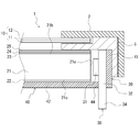
- FIG. 2 is a cross-sectional view of the main part of the liquid crystal display device of FIG.
- a liquid crystal display device 1 includes a liquid crystal display panel 10 as a display panel, and an edge light type illumination device (hereinafter simply referred to as an illumination device) for irradiating the liquid crystal display panel 10 with light from the back. 20).
- the liquid crystal display panel 10 and the lighting device 20 are integrally held by the bezel 2.
- the bezel 2 has a frame shape that covers the periphery of the liquid crystal display panel 10, and ensures the strength of the entire liquid crystal display device 1 together with the chassis 40 included in the lighting device 20.
- the edge light type illuminating device 20 includes a light guide plate 21, an LED light source 30 disposed at a side (edge side) end of the light guide plate 21, a reflection sheet 22, optical sheets 23 to 25, and the like. And the chassis 40 is housed in an exterior material.
- one side surface on which the LED light source 30 is disposed is a light incident surface 21a
- the front surface side is a light emitting surface 21b
- the bottom surface side is a light reflecting surface 21c.
- the chassis 40 is formed in a box shape including a bottom surface portion 42 having a horizontally long rectangular shape in plan view and side surface portions 41, 41, 41, 41 erected from four sides around the bottom surface portion 42. .
- the chassis 40 is formed as an opening with a surface facing the bottom surface portion 42 opened to the outside.
- the chassis 40 is formed by forming a metal plate material such as aluminum or iron into a shallow box shape by bending or the like.
- the opening side of the chassis 40 is referred to as the front surface, and the surface facing the opening side of the chassis 40 is referred to as the bottom surface portion.
- the front surface of the chassis 40 is a surface from which light is emitted in the edge light type illumination device 20. That is, the edge light type illumination device 20 of the present invention is a surface light source having a front surface formed as a light emitting surface.
- the LED light source 30 uses a plurality of LEDs (light emitting diodes) 31 as light emitting elements.
- the LED 31 has a package structure in which an LED chip that generates blue light is sealed with a transparent resin mixed with a yellow phosphor, and is formed to emit white light from a light emitting surface.
- the LED light source 30 has a belt-like substrate 32 and a heat radiation portion 34 composed of a protrusion protruding outward from the substrate 32 in the short direction.
- the shape of the heat radiating portion 34 is a thin plate having a square shape in plan view.
- the heat radiating portion 34 is formed integrally with the substrate 32 and is mounted so as to protrude to the chassis bottom surface side (downward in FIG. 2).
- the LED 31 is mounted on the substrate 32 so that the light exit surface faces the light incident surface 21 a on the side surface of the light guide plate 21.
- the light source 30 is mounted on the chassis 40 so that the surface of the substrate 32 is parallel to the side surface portion 41 of the chassis 40.
- the heat radiating portion 34 is inserted, and a heat radiating portion insertion hole 44 penetrating the bottom surface portion 42 to the back side is provided. As shown in FIG. 2, the heat radiating portion 34 is disposed outside the chassis 40 through the insertion hole 44 and is exposed to the outside. Since the heat radiating portion 34 is arranged and exposed outside the chassis 40 in this manner, the heat generated by the LED 31 is directly radiated to the outside of the chassis 40 via the substrate 32 and the heat radiating portion 34, so that the heat radiating portion 32 The cooling efficiency could be improved.
- the substrate 32 and the heat radiating portion 34 are integrally formed. It is not necessary to join firmly and the number of parts can be reduced.
- the LED light source 30 is attached, it is only necessary to lead the heat dissipating part 32 to the outside from the heat dissipating part insertion hole 44, and it is not necessary to firmly bond the substrate to the chassis, so it is necessary to firmly fix the screws. And easy to assemble.
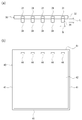
- FIG. 3 shows an example of the LED light source and chassis of the edge light type illumination device of the present invention, (a) is a plan view showing the substrate surface of the LED light source, and (b) is a plan view of the chassis.
- the LED light source 30 has LEDs 31, 31, 31, 31 mounted in a line at a predetermined interval in the longitudinal direction of the substrate 32.
- the LED 31 is mounted on the surface of the substrate 32 so that the light emitting surface is on the front side.
- the chassis 40 is formed so that the size of the bottom surface portion 42 can accommodate the light guide plate 21 and the light source 30 at the side end portion of the light guide plate 21. Further, the thickness of the chassis 40 (height of the side surface portion 42) is formed so as to accommodate the light guide plate 21, the various optical sheets 23 to 25, and the like.
- the chassis 40 has a heat radiation portion insertion hole 44 for leading the heat radiation portion 34 of the light source 30 to the outside of the chassis 40 on the bottom surface portion 42.
- the heat radiating portion insertion hole 44 is provided in the vicinity of one side surface portion 41 of the chassis where the LED light source 30 is disposed.
- the heat radiation part insertion hole 44 is formed at a position corresponding to the position of the heat radiation part 34.
- the shape of the heat radiating portion insertion hole 44 is a long hole in which the length in the longitudinal direction is slightly larger than the width W of the heat radiating portion, and the width in the short direction is slightly thicker than the thickness of the heat radiating portion. is there.
- the substrate 32 is formed from a strip-like elongated wiring substrate.
- a resist film (sometimes referred to as an insulating film) is formed on the entire surface of the base material (base), and an electric circuit (not shown) using a conductor is formed in a predetermined wiring pattern on the surface of the resist film. Yes.
- the plurality of LEDs 31, 31, 31, 31 are electrically connected to a conductor electric circuit.
- the surface of the substrate 32 is covered with a resist film (sometimes referred to as an insulating film) except for a portion connected to the electrode of the LED 31.
- the substrate 32 is preferably a metal substrate in terms of cooling efficiency and cost.
- the insulating film epoxy resin, epoxy resin with filler, polyimide, glass epoxy, or the like is used.
- the conductor copper foil, composite foil, conductor paste, or the like is used.
- the LED light source 30 is provided so that the heat radiating portion 34 of the substrate 32 protrudes below the substrate 32 at a position adjacent to the LED 31 corresponding to the position of the LED 31. That is, the same number of heat radiation portions 34 as the number of LEDs 31 are provided. Thus, if the heat radiating part 34 corresponds to the position of the LED 31 and is adjacent to the LED 31, the cooling efficiency is good.
- the length W of the heat radiating portion 34 in the longitudinal direction of the substrate (sometimes referred to as the protruding width W of the heat radiating portion) is preferably substantially the same as the length of one LED 31. .
- the length of the LED 31 is about 40 to 60 mm
- the protrusion width W of the heat radiating section is preferably about 30.0 to 60.0 mm.
- the projecting length L of the heat dissipating part 34 projecting outward from the substrate 32 is preferably formed such that the heat dissipating part 34 protrudes 10.0 to 40.0 mm or more from the outer surface of the chassis bottom part 42. From this point, the protrusion length L of the heat radiation part is particularly preferably 10.0 to 50.0 mm.
- FIG. 4 shows the LED light source of FIG. 3, (a) is a plan view showing a part of the substrate surface, and (b) is a sectional view taken along line BB of (a).
- the heat radiating portion 34 of the LED light source 30 is integrally formed by extending the substrate 32.
- the inside of the substrate 32 is a metal base, and the heat radiating portion 34 is formed as a metal base in the same manner as the substrate 32.
- the surface of the LED light source 30 on the LED 31 side has a resist film 35 formed on the surface of the substrate 32, but the surface of the heat radiating portion 34 has a resist film removed to form a metal base.
- the surface of 36 is exposed to the outside.
- the heat dissipation of the substrate 32 can be further improved.
- the heat conductivity of the heat radiating portion 34 is 1 W ⁇ m ⁇ 1 ⁇ K ⁇ 1 or more. From the viewpoint, it is preferably 2 W ⁇ m ⁇ 1 ⁇ K ⁇ 1.
- the thermal conductivity of the heat radiating portion can be set to the above range by using a metal-based substrate 32 and appropriately selecting a base material.
- FIG. 5 shows another embodiment of the LED light source
- (a) is a plan view showing a part of the substrate surface
- (b) is a cross-sectional view taken along line BB in (a)
- (c) is shown in FIG. It is CC sectional view taken on the line of (a). 4 to 6 show only one LED portion.
- the LED light source 32 of the aspect shown in FIG. 5 is a thing in which the thermal radiation part 34 is formed with the material with high heat conductivity.
- the heat dissipating part 34 shown in FIGS. 5A to 5C is composed of a heat dissipating part main body 34 a outside the substrate 32 and a mounting part 34 b inserted and fixed between the LED 31 and the substrate 32. ing.
- the width of the heat radiating portion main body 34a is formed to be substantially the same as the width of the LED 31, and the width of the mounting portion 34b is formed to be narrower than that.
- the resist film remains on the surface of the substrate 32 except for the mounting portion 34b.
- the contact portion of the substrate 32 with the mounting portion 34b has no resist film. That is, the mounting portion 34b is in direct contact with a base material such as a metal base of the substrate.
- the LED 31 is connected to a wiring (not shown) in which electrodes 31b such as an anode and a cathode are formed on the surface of the substrate 32.
- the thermal conductivity is preferably 80 W ⁇ m ⁇ 1 ⁇ K ⁇ 1 or more.
- the heat conductivity of the heat dissipating part is more preferably 200 W ⁇ m ⁇ 1 ⁇ K ⁇ 1 or more. Examples of such a material include metals such as aluminum, copper, iron, stainless steel, zinc, gold, silver, and copper.
- a mounting part 34b is joined to the surface of the substrate 32 or the back side of the LED.
- the heat of the LED 31 is transmitted to the heat radiating portion main body 34 a via the mounting portion 34 b in contact with the back surface of the LED 31, and is radiated to the outside of the chassis 40.
- the heat conductivity of the heat radiating part 34 is high, heat generated from the LED 31 can be efficiently radiated to the outside of the chassis 40.
- FIG. 6 shows another embodiment of the LED light source, (a) is a plan view showing a part of the substrate surface, and (b) is a sectional view taken along the line BB of (a).
- the heat radiating portion 34 can be formed in a comb shape. By forming the heat dissipating part in a comb shape, the space formed around the heat dissipating part 34 is increased, and cooling can be performed efficiently.
- the heat radiating portion 34 is formed integrally with the substrate 32 and has the same layer structure as the substrate 32.
- 6 (a) and 6 (b) is a comb-like shape having three teeth, the number of teeth is not particularly limited to three, and may be formed to four or more. .
- FIG. 7 is a cross-sectional view showing another embodiment of the edge light type illumination device of the present invention and showing the vicinity of an LED light source.
- the edge light device 10 may be configured such that the heat radiating portion 34 disposed outside the chassis 40 is bent toward the chassis bottom surface portion 42 side.
- the heat radiating portion 34 can be bent substantially at a right angle so as to be parallel to the chassis bottom surface portion 42, for example. Bending the heat radiating portion 34 in this manner reduces the heat radiation efficiency, but the thickness of the edge light type illumination device 10 in the thickness direction can be reduced. This aspect is effective when the module is to be thinned.
- the LED light source 30 is attached to the chassis, and after the heat radiating portion 34 is led out of the chassis 40 from the heat radiating portion insertion hole and assembled, The heat radiating part 34 may be bent.
- the length of the heat radiating portion 34 of the LED light source 30, the protruding position, etc. are not limited to the above modes.
- the number and position of the heat radiating units 34 may not correspond to the number and position of the LEDs 31.
- the number of LEDs 31 of the LED light source 30 is not limited to four or five, but may be plural.
- the shape of the heat radiation part 34 is not limited to a square shape, a comb-tooth shape, etc., It can form in various shapes.
- the light guide plate 21 is composed of a rectangular transparent thin plate.
- the light guide plate 11 is formed from a transparent plastic such as acrylic resin, polycarbonate resin, or cycloolefin resin.
- the thickness of the light guide plate 11 is usually about 3 to 4 mm.
- a reflection pattern is formed on the light reflecting surface 21c of the light guide plate 21. Further, a reflection sheet 22 separate from the light guide plate 21 is disposed on the reflection pattern side of the light guide plate 21.
- the reflection pattern is formed on the light guide plate 21 by printing such as screen printing.
- the reflection pattern is composed of a white dot pattern composed of white dots.
- the pattern such as the size and position of the dots of the reflection pattern scatters and reflects the light emitted from the LED 31, and the light emitted from the light emitting surface 21b is emitted uniformly over the entire surface, for example, In the vicinity, the dot diameter is small, and in the distance of the light source, the dot diameter is large.
- the reflection pattern may be formed by injection molding or the like.
- the reflection sheet 22 is made of a plastic sheet having reflectivity with a thickness of about 0.1 to 2 mm. Of the light from the LED 31 incident on the light guide plate 21, the reflection sheet 22 is light that has been diffusely reflected by the reflection pattern and is not directed toward the light emission surface 21 b, but passes through the light reflection surface 21 c on the opposite side. To reflect.
- the reflective sheet 22 is a mirror-reflective reflective sheet such as a polyester film deposited with a metal such as aluminum or silver, a white polyester film, an ultra-white polyester film, an interface multiple reflection type reflective sheet, a porous PP, a micro-foamed polyester sheet, or the like.
- An irregular reflection sheet or the like can be used.
- a diffusion sheet 23, a lens sheet 24, a polarization selective reflection sheet 25, or the like can be used as the optical sheets 23 to 25, for example, a diffusion sheet 23, a lens sheet 24, a polarization selective reflection sheet 25, or the like. These sheets are sequentially arranged on the light emitting surface 21 b side of the light guide plate 21.
- the diffusion sheet 23 further uniformizes the luminance in the surface direction of the emitted light.
- the lens sheet 24 collects the light transmitted through the diffusion sheet 23 and increases the luminance.
- the polarization selective reflection sheet 24 transmits polarized light in a specific direction and reflects other polarized light so that the light reaching the liquid crystal display panel 10 is not absorbed by the polarizing plate of the liquid crystal display panel.
- the optical sheets 23 to 25, the light guide plate 21, and the reflection sheet 22 are fixed to the chassis 40 by the frame 5 in a state of being laminated in this order.
- the frame 5 is formed in a frame shape (frame shape) extending along the outer peripheral end portion of the light guide plate 21 and presses the outer peripheral end portions of the optical sheets 23 to 25 and the light guide plate 11 from the front side over almost the entire periphery. It is possible.
- the frame 5 is made of, for example, black synthetic resin and has a light shielding property. Further, the frame 5 can receive the back surface of the outer peripheral end portion of the liquid crystal display panel 10 with its frame-shaped front surface (see FIG. 1).
- the display device of the present invention can be configured as a liquid crystal display device using a liquid crystal panel as the display panel.
- the liquid crystal display device 1 includes a liquid crystal display panel 10 and an edge light type illumination device 20 that is a backlight device for irradiating the liquid crystal display panel 10 with light.
- the liquid crystal display panel 10 is disposed on the light emission surface 21 b side on the front side of the edge light type illumination device 20.
- the liquid crystal display panel 3 has a horizontally long rectangular shape when viewed from above.
- the liquid crystal display panel 10 includes a pair of transparent substrates, each composed of a thin film transistor (TFT) array substrate 11 and a color filter (CF) substrate 12, which are bonded in parallel with a predetermined distance therebetween. It has a liquid crystal layer (not shown) in which liquid crystal is sealed.
- TFT thin film transistor
- CF color filter
- a plurality of TFTs and pixel electrodes are formed in a matrix on the TFT array substrate 11, and a plurality of colored patterns are formed on the CF substrate 12 in a matrix, and a common electrode is formed on almost the entire surface.
- An image can be displayed by controlling the orientation of the liquid crystal by changing the voltage applied between the pixel electrode and the common electrode.
- polarizing plates are disposed on the front and back surfaces of the liquid crystal display panel 10 (not shown).
- the frame 5 and the bezel 2 are screwed to the chassis side surface portion 41. Further, on the rear surface of the chassis 40, a power supply board 51 for supplying power to the LED light source 30, a control board 52 for driving the liquid crystal display panel 3, and the like are disposed.
- the edge light type illumination device 10 As shown in FIG. 2, in the edge light type illumination device 10, light emitted from the LED 31 of the LED light source 30 enters the light guide plate 21 from the light incident surface 21 a on the side surface of the light guide plate 21.
- the light incident on the inside of the light guide plate 21 travels in the light guide plate 21 and is scattered by the reflection pattern, and is repeatedly reflected between the light emitting surface 21b and the light reflecting surface 21c by the reflection sheet 22, and is planarly formed therein.
- the light is emitted in a planar shape from the light exit surface 21 b of the spread light guide plate 21.
- the planar light radiated from the light emitting surface 21b passes through the diffusion sheet 23, the lens sheet 24, the polarization selective reflection sheet 25, etc., and improves the optical characteristics such as luminance and uniformity, and the liquid crystal display panel 10. Irradiated to the back side.
- the display device of the present invention includes the edge light type illumination device as an external light irradiation device that irradiates the display panel with external light.
- the display device of the present invention can be suitably used for a large television or the like as a liquid crystal display device.
- the display device of the present invention is not limited to a liquid crystal display device, and can be used for various display devices as long as the display device is a combination of a display panel and an external light irradiation device.
Landscapes
- Physics & Mathematics (AREA)
- General Physics & Mathematics (AREA)
- Optics & Photonics (AREA)
- Planar Illumination Modules (AREA)
- Liquid Crystal (AREA)
Abstract
光源を効率良く冷却し輝度を更に向上させることが可能であると共に、構造が簡単であり組み立て作業も容易である、エッジライト型照明装置及び表示装置を提供する。 底面部42と側面部41を有する箱形のシャーシ40の内側に導光板21と、帯状の基板32に複数個のLED31が装着されているLED光源30とを有し、LED光源30が、基板32から基板短手方向外方に突出する突起からなる放熱部34を有し、シャーシ40の底面部42に、前記放熱部34が挿通し前記底面部42を貫通する放熱部挿通孔44を設け、前記放熱部34が前記放熱部挿通孔44を通して前記シャーシ40の外側に配置されるようにして、エッジライト型照明装置20を構成した。
Description
本発明は、エッジライト型照明装置及び表示装置に関し、特に液晶表示装置等の面光源として好適なエッジライト型照明装置及び該照明装置を用いた表示装置に関する。
エッジライト型(サイドライト方式ということもある)照明装置は、液晶表示装置等の表示装置において、表示パネルに外部光を照射するためのバックライト装置(面光源装置)として広く用いられている。
エッジライト型のバックライト装置は、発光ダイオード(LED)等の光源と導光板から構成され、該光源からの光を導光板の側面端部方向から入射させ、導光板の表面から出射させて発光するようにすることで、面発光に変換している。そのため光源を導光板の背面に配置した直下型のバックライト装置と比較して、厚みを薄く形成することができる。
エッジライト型のバックライト装置は、光源のLEDの発熱量が大きくなると、温度が上昇し、LEDの発光効率が低下する。更にLEDの発熱量が大きくなると、LED基板が過熱し、パーケージの不良や、導光板の損傷を引き起こすことになる。そこで、LED等の冷却効率を向上させたエッジライト型照明装置が公知である(例えば、特許文献1参照)。
図8に示すように、特許文献1に記載のエッジライト型照明装置は、背面フレーム201の上に、サブシャーシ202を介してLED基板203や導光板205が取り付けられている。LED基板203にはLED204が実装され、該LED基板203の底面はサブシャーシ202に接合している。LED基板203のサブシャーシ202と接合している面と反対の面は、放熱板207が取り付けられ、その底面がサブシャーシ202に接合している。
上記特許文献1に記載されているエッジライト型照明装置は、LED基板203からの発熱をサブシャーシ202や背面フレーム201に伝達することで放熱して、LED基板203を冷却するように構成されている。
エッジライト型照明装置は、更なる輝度の向上が要望されている。エッジライト照明装置の輝度を向上させるためには、LEDの発光量を高める必要がある。LEDの発光量が高くなると、発熱が大きくなるため、光源の冷却効率を高くする必要がある。
しかしながら上記特許文献1に記載のエッジライト型照明装置のように、放熱板を介してLED基板を冷却する方式の場合、LED基板と放熱板が接触している界面の熱伝達効率を更に高めるのは困難である。LED基板の発熱を熱伝導のみで冷却効果を向上させるには限界があるという問題があった。
また上記の放熱板を介してLED基板を冷却する方式は、放熱板を取り付ける際に、LED基板やシャーシ等と確実に界面を接触させる必要があるので、ビス等を用いて放熱板とLED基板やシャーシを強く固定する必要がある。そのため、ビス等の部品点数が多くなり、組立作業が繁雑になってしまうという問題があった。
上記実状に鑑み、本発明が解決しようとする課題は、エッジライト型照明装置において、光源を効率良く冷却し輝度を更に向上させることが可能であると共に、構造が簡単であり組み立て作業も容易である、エッジライト型照明装置及び表示装置を提供することにある。
本発明のエッジライト型照明装置は、
底面部と側面部を有する箱形のシャーシの内側に、導光板と、基板に複数個のLEDが装着されているLED光源とを有するエッジライト型照明装置において、
前記LED光源が、帯状の基板と、該基板から基板短手方向外方に突出する突起からなる放熱部とを有し、
前記シャーシの底面部に、前記放熱部が挿通し前記底面部を貫通する放熱部挿通孔が設けられ、
前記放熱部が前記放熱部挿通孔を通して前記シャーシ外側に配置されていることを特徴とするエッジライト型照明装置。
ことを要旨とするものである。
底面部と側面部を有する箱形のシャーシの内側に、導光板と、基板に複数個のLEDが装着されているLED光源とを有するエッジライト型照明装置において、
前記LED光源が、帯状の基板と、該基板から基板短手方向外方に突出する突起からなる放熱部とを有し、
前記シャーシの底面部に、前記放熱部が挿通し前記底面部を貫通する放熱部挿通孔が設けられ、
前記放熱部が前記放熱部挿通孔を通して前記シャーシ外側に配置されていることを特徴とするエッジライト型照明装置。
ことを要旨とするものである。
上記エッジライト型照明装置において、前記放熱部が、前記LEDの位置に隣接して形成されていることが好ましい。
上記エッジライト型照明装置において、前記放熱部表面のレジスト膜が除去されていることが好ましい。
上記エッジライト型照明装置において、前記放熱部が熱伝導率の高い材質により形成されていて、前記基板に装着するための装着部と放熱部本体とを有していることが好ましい。
上記エッジライト型照明装置において、前記放熱部が櫛歯状に形成されていることが好ましい。
上記エッジライト型照明装置において、前記放熱部がシャーシの底面部側に折り曲げられていることが好ましい。
本発明の表示装置は、上記のエッジライト型照明装置を、表示パネルの外光照射装置として用いたことを要旨とするものである。
上記表示装置において、前記表示パネルが液晶表示パネルであることが好ましい。
本発明のエッジライト型照明装置は、前記LED光源の基板が、帯状の基板と、該基板から基板短手方向外方に突出する突起からなる放熱部とを有し、前記シャーシの底面部に、前記放熱部が挿通し前記底面部を貫通する放熱部挿通孔が設けられ、前記放熱部が前記放熱部挿通孔を通して前記シャーシ外側に配置されている構成を有することにより、放熱部によってLEDの発熱を放熱させることができる。特に前記放熱部がシャーシの外側に配置されているので、LEDの熱がシャーシの内部に溜まることなく、光源の熱をシャーシ外部に放熱して冷却効率を高めることができる。本発明のエッジライト型照明装置は、光源からの熱を効率良く放熱することができるので、光源の冷却効率が向上し、更なる輝度の向上を図ることが可能である。
更に本発明のエッジライト型照明装置は、組立の際に放熱部が放熱部挿通孔から外部に導出するようにLED光源をシャーシに装着するだけで良い。従って、従来のように熱伝導を良くするためにLED基板と放熱板の接合やシャーシと放熱板の接合を強固に行う必要がないので、構造が簡単であり、ビス等の部品点数が多くなることもなく、また組み立て作業も容易に行うことができる。
本発明の表示装置は、上記のエッジライト型照明装置を外光照射装置として用いたものであるから、輝度を向上させることができ、表示品位の優れた表示画像を得ることができる。
以下、本発明の実施例について図面を参照して詳細に説明する。図1は本発明の表示装置の一実施例としての液晶表示装置を模式的に示した分解斜視図であり、図2は図1の液晶表示装置の要部断面図である。図1及び図2に示すように、液晶表示装置1は、表示パネルとして液晶表示パネル10と、この液晶表示パネル10に背面から光を照射するためのエッジライト型照明装置(以下、単に照明装置ということもある。)20を有する。液晶表示パネル10と照明装置20がベゼル2により一体的に保持されている。ベゼル2は、液晶表示パネル10の周縁に被せられる額縁形状を有しており、照明装置20が備えるシャーシ40と共に液晶表示装置1全体の強度を確保するものである
エッジライト型照明装置20は、導光板21と、該導光板21の側面方向(エッジ側)端部に配置されたLED光源30と、反射シート22と、光学シート23~25等が、フレーム5とシャーシ40により構成される外装材の内部に収納されている。導光板21は、LED光源30が配設されている側の一側面が光入射面21aであり、前面側が光出射面21bであり、底面側が光反射面21cとなっている。
シャーシ40は、平面視が横長の長方形状を有する底面部42と該底面部42の周囲の四辺から立設している側面部41、41、41、41とからなる箱形に形成されている。シャーシ40は、底面部42と対向する面が外側に開口していて、開口部として形成されている。シャーシ40は、アルミニウム、鉄等の金属製板材を折り曲げ加工等によって、浅底の箱形状に成形したものである。
尚、本発明のエッジライト型照明装置20では、シャーシ40の開口部側を前面といい、シャーシ40の開口部側と対向する面を底面部という。シャーシ40の前面は、エッジライト型照明装置20において光が放射される面である。すなわち本発明のエッジライト型照明装置20は、前面が発光面として形成されている面光源である。
LED光源30は、発光素子として複数のLED(発光ダイオード)31を用いたものである。LED31は、青色光を発生させるLEDチップを、黄色蛍光体が混合された透明樹脂で密封したパッケージ構造を有しており、発光面から白色光を放射するように形成されている。
LED 光源30は、帯状の基板32と、該基板32から短手方向外方に突出する突起からなる放熱部34を有している。放熱部34の形状は、平面視が方形である薄板状である。放熱部34は、基板32と一体に形成されておりシャーシ底面側(図2の下方)に突出するように装着されている。
LED31は、光出射面が導光板21の側面の光入射面21aと対向するように、基板32に装着されている。光源30は、基板32面がシャーシ40の側面部41と平行になるように、シャーシ40に装着されている。
シャーシの底面部42には、上記放熱部34が挿通し、前記底面部42を背面側に貫通する放熱部挿通孔44が設けられている。図2に示すように、放熱部34は挿通孔44を通してシャーシ40の外側に配置されていて外部に露出している。このように放熱部34がシャーシ40の外側に配置されて露出していることにより、LED31の発熱を、基板32、放熱部34を介してシャーシ40の外部に直接放熱して、放熱部32の冷却効率を向上させることができた。
また、LED光源30をエッジライト型照明装置20に装着する場合、基板32と放熱部34は一体に形成されているので、別部品の放熱板等をLED光源30の基板32やシャーシ40等と強固に接合する必要がなく、部品点数を減少させることができる。しかも、LED光源30の取り付けの際、放熱部32を放熱部挿通孔44から外部に導出させるだけでよく、基板をシャーシと強固に接合する必要がないので、ビス止め等も強固に行う必要がなく、組立も容易である。
図3は、本発明のエッジライト型照明装置のLED光源とシャーシの一例を示し、(a)はLED光源の基板表面を示す平面図であり、(b)はシャーシの平面図である。図3(a)に示すようにLED光源30は、LED31、31、31、31が、基板32の長手方向に所定の間隔で一列に装着されている。LED31は、発光面が表側になるように、基板32の表面に装着されている。
シャーシ40は、底面部42の大きさが、導光板21と、該導光板21の側面端部の光源30とを収納可能な大きさに形成されている。またシャーシ40の厚さ(側面部42の高さ)は、導光板21、各種光学シート23~25等が収納可能な大きさに形成されている。
図3(b)に示すように、シャーシ40は、底面部42に光源30の放熱部34をシャーシ40の外側に導出するための放熱部挿通孔44を有する。放熱部挿通孔44は、LED光源30が配設されるシャーシの一側面部41近傍に設けられている。
放熱部挿通孔44は、放熱部34の位置に対応する位置に形成されている。放熱部挿通孔44の形状は、長手方向となる長さが放熱部の幅Wよりも若干大きく形成され、短手方向となる幅が放熱部の厚みよりも若干厚く形成されている長孔である。
基板32は、帯状の細長い配線基板から形成されている。基板32は、基材(ベース)の表面全体にレジスト膜(絶縁膜ということもある)が形成され、該レジスト膜の表面に導体による電気回路(図示しない)が所定の配線パターンに形成されている。複数のLED31、31、31、31は、導体の電気回路と電気的に接続されている。基板32の表面は、LED31の電極と接続する部分を除いて、レジスト膜(絶縁膜ということもある)により被覆されている。
基板32は、基材の種類により、樹脂系基板、セラミック系基板、金属系基板等の各種基板が用いられる。基板32は、冷却効率及びコストの点から金属系基板が好ましい。上記絶縁膜は、エポキシ樹脂、フィラー入りエポキシ樹脂、ポリイミド、ガラスエポキシ等が用いられる。上記導体は、銅箔、複合箔、導体ペースト等が用いられる。
図3(a)に示す態様のLED光源30は、基板32の放熱部34は、LED31の位置に対応してLED31に隣接する位置に基板32の下方に突出するように設けられている。すなわち放熱部34の数は、LED31の数と同じ数だけ設けられている。このように放熱部34が、LED31の位置に対応し、LED31に隣接していると、冷却効率が良い。
図3(a)に示すように、放熱部34の基板長手方向の長さW(放熱部の突出幅Wということもある)は、一つのLED31の長さと略同じ長さであることが好ましい。通常、LED31の長さは、40~60mm程度であり、放熱部の突出幅Wは、30.0~60.0mm程度に形成するのが好ましい。また基板32から外方に突出する放熱部34の突出長さLは、シャーシ底面部42の外表面から該放熱部34が10.0~40.0mm以上飛び出す長さに形成するのが好ましい。このような点から具体的に好ましい放熱部の突出長さLは、10.0~50.0mmである。
図4は、図3のLED光源を示し、(a)は基板表面の一部を示す平面図であり、(b)は(a)のB-B線断面図である。図4(a)、(b)に示すように、LED光源30の放熱部34は、基板32が延設されて一体に形成されている。基板32は内部が金属ベースであり、放熱部34も基板32と同様に、金属ベースとして形成されている。図3(b)に示すように、LED光源30のLED31側の表面は、基板32の表面はレジスト膜35が形成されているが、放熱部34の表面はレジスト膜が除去されて、金属ベース36の表面が外部に露出している。このように放熱部34の表面のレジスト膜が除去されていると、シャーシ40の外部で金属ベース36表面を直接露出させることができるので、放熱部の金属ベースがレジスト膜に覆われている場合と比較して、基板32の放熱性を更に向上させることができる。
放熱部34が基板32に延設されていて、基板32と同じ材質により形成されている場合、放熱部34の熱伝導率は1W・m-1・K-1以上であるのが放熱性の点から好ましく、更に好ましくは2W・m-1・K-1である。放熱部の熱伝導率は、金属ベースの基板32を用い、基材を適宜選択することで上記範囲とすることができる。
図5は、LED光源の他の態様を示し、(a)は基板表面の一部を示す平面図であり、(b)は(a)のB-B線断面図であり、(c)は(a)のC-C線断面図である。尚、図4~6は、一つのLEDの部分のみを示した。図5に示す態様のLED光源32は、放熱部34が熱伝導率の高い材質により形成されているものである。図5(a)~(c)に示す放熱部34は、基板32の外方にある放熱部本体34aと、LED31と基板32の間に挿入されて固定されている装着部34bとから構成されている。
図5(a)に示すように、放熱部本体34aの幅は、LED31の幅と略同じに形成され、装着部34bの幅はそれよりも狭い幅に形成されている。図5(c)に示すように、基板32の表面は、装着部34bの部分を除いて、レジスト膜が残っている。基板32の装着部34bとの接触部分は、レジスト膜がない。すなわち、装着部34bは、基板の金属ベース等の基材と直接接触している。尚、LED31はアノード、カソード等の電極31bが基板32の表面に形成されている配線(図示せず)と接続されている。
図5に示す態様のLED光源30の放熱部34は、熱伝導率の高い材質として、熱伝導率が80W・m-1・K-1以上であるのが好ましい。さらに好ましい放熱部の熱伝導率は200W・m-1・K-1以上である。このような材質として、例えば、アルミニウム、銅、鉄、ステンレス、亜鉛、金、銀、銅等の金属が挙げられる。
図5に示す放熱部34は、基板32の表面或いはLEDの背面側に装着部34bが接合されている。LED31の熱は、LED31の背面に接触している装着部34bを介して放熱部本体34aに伝わり、シャーシ40の外部に放熱される。この場合、放熱部34の熱伝導率が高いので、LED31からの発熱をシャーシ40の外部に効率良く放熱することができる。
図6は、LED光源の他の態様を示し、(a)は基板表面の一部を示す平面図であり、(b)は(a)のB-B線断面図である。図6(a)、(b)に示すように放熱部34は、櫛歯状に形成することができる。放熱部を櫛歯状に形成することで、放熱部34の周囲に形成される空間が大きくなり、冷却を効率良く行うことができる。
図6(a)、(b)に示す態様のLED光源において、放熱部34は、基板32と一体に形成されており、基板32と同様の層構造に形成されている。図6(a)、(b)に示す放熱部34は3本の歯を有する櫛歯状であるが、この歯の数は特に3本に限定されず、4本以上に形成してもよい。
図7は、本発明のエッジライト型照明装置の他の態様を示し、LED光源付近を示す断面図である。図7に示すようにエッジライト装置10は、シャーシ40の外部に配置されている放熱部34を、シャーシ底面部42側に折り曲げてもよい。図7に示すように、この放熱部34は、例えば、シャーシ底面部42と平行になるように、略直角に折り曲げることができる。このように放熱部34を折り曲げることにより、放熱効率は低下するが、エッジライト型照明装置10の厚み方向の厚さを薄く形成することができる。この態様は、モジュールの薄型化を図る場合、効果的である。
図7に示すように、放熱部34を折り曲げた状態に形成するには、LED光源30をシャーシに装着し、放熱部34を放熱部挿通孔からシャーシ40の外部に導出して組み立てた後に、放熱部34を折り曲げ加工すればよい。
本発明では、LED光源30の放熱部34の長さ、突出位置等は、上記態様に限定されるものではない。例えば放熱部34の数や位置が、LED31の数や位置と対応しなくても良い。またLED光源30のLED31の数等も、4或いは5個に限定されるものではなく、複数個であれば良い。また、放熱部34の形状は、方形状、櫛歯状等に限定されず、各種の形状に形成することができる
以下、エッジライト型照明装置20のその他の構成について説明する。導光板21は、方形状の透明な薄板から構成される。導光板11はアクリル樹脂、ポリカーボネート樹脂、シクロオレフィン樹脂等の透明プラスチックから形成される。導光板11の厚さは、通常、3~4mm程度に形成される。
導光板21の光反射面21cには、図示しないが、反射パターンが形成されている。更に導光板21の反射パターン側には、導光板21とは別体の反射シート22が配置されている。反射パターンは、導光板21に、スクリーン印刷等の印刷により形成されている。
反射パターンは、白色ドットからなる白色ドットパターンにより構成されている。反射パターンのドットの大きさ、位置等のパターンは、LED31から出た光を散乱させて反射させ、光出射面21bから放射される光が、面全体で均一に放出するように、例えば光源の近くは、ドット径が小さく、光源の遠くはドット径が大きく成るように形成されている。反射パターンは、射出成形等で形成してもよい。
反射シート22は、厚さが0.1~2mm程度の反射性を有するプラスチックシートからなる。反射シート22は導光板21に入射したLED31からの光のうち、反射パターンで乱反射した光が、光出射面21bに向かわずに反対側の光反射面21cから抜ける光を、光出射面21b側に反射させる。
反射シート22は、アルミニウムや銀等の金属を蒸着したポリエステルフィルム等の鏡面反射の反射シート、白色ポリエステルフィルム、超白色ポリエステルフィルム、界面多重反射型反射シート、多孔質PP、微発泡ポリエステルシート等の乱反射の反射シート等を用いることができる。
光学シート23~25は、例えば、拡散シート23、レンズシート24、偏光選択性反射シート25等を用いることができる。これらのシートは、導光板21の光出射面21b側に順次配置されている。拡散シート23は、出射光の面方向における輝度をさらに均一化させるものである。レンズシート24は、拡散シート23を透過した光を集光し、輝度を高めるものである。偏光選択性反射シート24は、液晶表示パネル10に到達した光が、液晶表示パネルの偏光板に吸収されないよう、特定方向の偏光を透過し、それ以外の偏光を反射させるためのものである。
光学シート23~25、導光板21及び反射シート22は、この順番で積層させた状態でフレーム5により、シャーシ40に固定されている。フレーム5は、導光板21の外周端部に沿って延在する枠状(額縁状)に形成されており、光学シート23~25および導光板11の外周端部をほぼ全周にわたって表側から押さえることが可能となっている。尚、フレーム5は、例えば黒色の合成樹脂製とされ、遮光性を有するものである。また、フレーム5は、液晶表示パネル10の外周端部の背面を、その枠状の前面で受けることが可能になっている(図1参照)。
本発明の表示装置は、図1及び図2に示すように、表示パネルとして液晶パネルを用いた液晶表示装置として構成することができる。図1に示すように液晶表示装置1は、液晶表示パネル10と、この液晶表示パネル10に光を照射するためのバックライト装置であるエッジライト型照明装置20とを備えている。液晶表示パネル10は、エッジライト型照明装置20の前面側の光出射面21b側に配置されている。
液晶表示パネル3は、平面に視て横長の長方形状を有している。この液晶表示パネル10は、薄膜トランジスタ(TFT)アレイ基板11とカラーフィルタ(CF)基板12とからなる一対の透明基板が所定の間隔を置いて平行に対向して貼り合わせられ、両透明基板間に液晶が封止された液晶層(図示しない)を有している。
上記TFTアレイ基板11には複数のTFTおよび画素電極がマトリクス状に形成され、上記CF基板12には複数の着色パターンがマトリクス状に形成されると共に、そのほぼ全面に共通電極が形成されており、これら画素電極と共通電極との間に印加する電圧を変化させて液晶を配向制御することで、画像を表示することができるようになっている。尚、液晶表示パネル10の表面と背面にはそれぞれ偏光板が配されている(図示しない)。
図1に示すように、シャーシ側面部41には、フレーム5及びベゼル2がネジ止めされる。またシャーシ40の背面には、LED光源30に電源を供給する電源基板51と、液晶表示パネル3を駆動するコントロール基板52等が配設されている。
図2に示すようにエッジライト型照明装置10は、LED光源30のLED31から放射された光が導光板21側面の光入射面21aから、導光板21の内部に入射する。導光板21の内部に入射した光は、導光板21内を進み反射パターンにより散乱し、反射シート22により光出射面21bと光反射面21cとの間で繰り返し反射し、その内部で平面状に広がり導光板21の光出射面21bから面状に放射される。光出射面21bから放射した面状の光は、拡散シート23、レンズシート24、偏光選択性反射シート25等を通過して、輝度、均一性等の光学的特性を向上させて液晶表示パネル10の背面側に照射される。
本発明の表示装置は、表示パネルに外光を照射する外光照射装置として、上記エッジライト型照明装置を備えるものである。本発明の表示装置は、液晶表示装置として大型テレビジョン等に好適に利用することができる。また本発明の表示装置は、液晶表示装置に限定されるものではなく、表示パネルと外光照射装置を組み合わせて構成される表示装置であれば、各種の表示装置に利用することができる。
Claims (8)
- 底面部と側面部を有する箱形のシャーシの内側に、導光板と、基板に複数個のLEDが装着されているLED光源とを有するエッジライト型照明装置において、
前記LED光源が、帯状の基板と、該基板から基板短手方向外方に突出する突起からなる放熱部とを有し、
前記シャーシの底面部に、前記放熱部が挿通し前記底面部を貫通する放熱部挿通孔が設けられ、
前記放熱部が前記放熱部挿通孔を通して前記シャーシ外側に配置されていることを特徴とするエッジライト型照明装置。 - 前記放熱部が、前記LEDの位置に隣接して形成されていることを特徴とする請求項1記載のエッジライト型照明装置。
- 前記放熱部表面のレジスト膜が除去されていることを特徴とする請求項1又は2記載のエッジライト型照明装置。
- 前記放熱部が熱伝導率の高い材質により形成されていて、前記基板に装着するための装着部と放熱部本体とを有していることを特徴とする請求項1~3のいずれか1項に記載のエッジライト型照明装置。
- 前記放熱部が櫛歯状に形成されていることを特徴とする請求項1~3のいずれか1項に記載のエッジライト型照明装置。
- 前記放熱部がシャーシの底面部側に折り曲げられていることを特徴とする請求項1~5のいずれか1項に記載のエッジライト型照明装置。
- 上記請求項1~6のいずれか1項に記載のエッジライト型照明装置を、表示パネルの外光照射装置として用いたことを特徴とする表示装置。
- 前記表示パネルが液晶表示装置であることを特徴とする請求項7記載の表示装置。
Applications Claiming Priority (2)
| Application Number | Priority Date | Filing Date | Title |
|---|---|---|---|
| JP2011032756 | 2011-02-18 | ||
| JP2011-032756 | 2011-02-18 |
Publications (1)
| Publication Number | Publication Date |
|---|---|
| WO2012111398A1 true WO2012111398A1 (ja) | 2012-08-23 |
Family
ID=46672335
Family Applications (1)
| Application Number | Title | Priority Date | Filing Date |
|---|---|---|---|
| PCT/JP2012/051543 Ceased WO2012111398A1 (ja) | 2011-02-18 | 2012-01-25 | エッジライト型照明装置及び表示装置 |
Country Status (1)
| Country | Link |
|---|---|
| WO (1) | WO2012111398A1 (ja) |
Cited By (1)
| Publication number | Priority date | Publication date | Assignee | Title |
|---|---|---|---|---|
| JP2019153505A (ja) * | 2018-03-05 | 2019-09-12 | シャープ株式会社 | 照明装置、表示装置、及びテレビ受信装置 |
Citations (3)
| Publication number | Priority date | Publication date | Assignee | Title |
|---|---|---|---|---|
| JP2007163620A (ja) * | 2005-12-12 | 2007-06-28 | Hitachi Displays Ltd | 液晶表示装置及びバックライト装置 |
| JP2007194067A (ja) * | 2006-01-19 | 2007-08-02 | Mitsubishi Electric Corp | 光源装置および液晶表示装置 |
| JP2010256813A (ja) * | 2009-04-28 | 2010-11-11 | Meitaku Kogyo Kk | ディスプレイ装置 |
-
2012
- 2012-01-25 WO PCT/JP2012/051543 patent/WO2012111398A1/ja not_active Ceased
Patent Citations (3)
| Publication number | Priority date | Publication date | Assignee | Title |
|---|---|---|---|---|
| JP2007163620A (ja) * | 2005-12-12 | 2007-06-28 | Hitachi Displays Ltd | 液晶表示装置及びバックライト装置 |
| JP2007194067A (ja) * | 2006-01-19 | 2007-08-02 | Mitsubishi Electric Corp | 光源装置および液晶表示装置 |
| JP2010256813A (ja) * | 2009-04-28 | 2010-11-11 | Meitaku Kogyo Kk | ディスプレイ装置 |
Cited By (1)
| Publication number | Priority date | Publication date | Assignee | Title |
|---|---|---|---|---|
| JP2019153505A (ja) * | 2018-03-05 | 2019-09-12 | シャープ株式会社 | 照明装置、表示装置、及びテレビ受信装置 |
Similar Documents
| Publication | Publication Date | Title |
|---|---|---|
| WO2009093583A1 (ja) | 表示装置および発光装置 | |
| JP2006011242A (ja) | 液晶表示装置 | |
| JPWO2012141094A1 (ja) | 光源モジュールおよびこれを備えた電子機器 | |
| US20130094187A1 (en) | Led backlight device and liquid crystal display device | |
| KR20090079568A (ko) | 광원 유닛, 그 제조 방법 및 이를 구비하는 표시 장치 | |
| JP2009266624A (ja) | 照明装置、液晶表示装置及び電子機器 | |
| JP2004349143A (ja) | 面状光源装置及び表示装置 | |
| JP2006310221A (ja) | エッジ入力型バックライト及び液晶表示装置 | |
| WO2012081395A1 (ja) | 照明装置およびこれを備えた液晶表示装置 | |
| JP4726456B2 (ja) | 液晶表示装置 | |
| WO2012128193A1 (ja) | 照明装置及び表示装置 | |
| JP2006064733A (ja) | 液晶表示装置 | |
| JP2007286467A (ja) | バックライト装置及び液晶表示装置 | |
| WO2012102193A1 (ja) | 照明装置、表示装置、及びテレビ受信装置 | |
| CN102200658A (zh) | 液晶显示装置 | |
| JP2006023654A (ja) | 液晶表示装置 | |
| KR101679077B1 (ko) | 백라이트 유닛 및 이를 구비한 액정표시장치 | |
| KR20120080366A (ko) | 발광 모듈, 이의 제조 방법 및 이를 포함하는 표시 장치 | |
| WO2011086790A1 (ja) | 照明装置、表示装置、テレビ受信装置 | |
| WO2012111398A1 (ja) | エッジライト型照明装置及び表示装置 | |
| KR20130003935A (ko) | 액정표시장치 | |
| KR101283068B1 (ko) | 블랑켓 일체형 방열회로기판, 이을 포함하는 백라이트 유닛 | |
| WO2012035898A1 (ja) | 照明装置およびこれを備えた液晶表示装置 | |
| CN104603520B (zh) | 光照射装置、背光装置以及显示装置 | |
| WO2012070331A1 (ja) | エッジライト型照明装置及び表示装置 |
Legal Events
| Date | Code | Title | Description |
|---|---|---|---|
| 121 | Ep: the epo has been informed by wipo that ep was designated in this application |
Ref document number: 12747447 Country of ref document: EP Kind code of ref document: A1 |
|
| NENP | Non-entry into the national phase |
Ref country code: DE |
|
| 122 | Ep: pct application non-entry in european phase |
Ref document number: 12747447 Country of ref document: EP Kind code of ref document: A1 |
|
| NENP | Non-entry into the national phase |
Ref country code: JP |