WO2012108182A1 - タッチパネルの制御回路およびそれを用いたタッチパネル入力装置、電子機器 - Google Patents
タッチパネルの制御回路およびそれを用いたタッチパネル入力装置、電子機器 Download PDFInfo
- Publication number
- WO2012108182A1 WO2012108182A1 PCT/JP2012/000804 JP2012000804W WO2012108182A1 WO 2012108182 A1 WO2012108182 A1 WO 2012108182A1 JP 2012000804 W JP2012000804 W JP 2012000804W WO 2012108182 A1 WO2012108182 A1 WO 2012108182A1
- Authority
- WO
- WIPO (PCT)
- Prior art keywords
- terminal
- voltage
- panel
- state
- current
- Prior art date
- Legal status (The legal status is an assumption and is not a legal conclusion. Google has not performed a legal analysis and makes no representation as to the accuracy of the status listed.)
- Ceased
Links
Images



Classifications
-
- G—PHYSICS
- G06—COMPUTING OR CALCULATING; COUNTING
- G06F—ELECTRIC DIGITAL DATA PROCESSING
- G06F3/00—Input arrangements for transferring data to be processed into a form capable of being handled by the computer; Output arrangements for transferring data from processing unit to output unit, e.g. interface arrangements
- G06F3/01—Input arrangements or combined input and output arrangements for interaction between user and computer
- G06F3/03—Arrangements for converting the position or the displacement of a member into a coded form
- G06F3/041—Digitisers, e.g. for touch screens or touch pads, characterised by the transducing means
- G06F3/0416—Control or interface arrangements specially adapted for digitisers
- G06F3/0418—Control or interface arrangements specially adapted for digitisers for error correction or compensation, e.g. based on parallax, calibration or alignment
- G06F3/04186—Touch location disambiguation
-
- G—PHYSICS
- G06—COMPUTING OR CALCULATING; COUNTING
- G06F—ELECTRIC DIGITAL DATA PROCESSING
- G06F3/00—Input arrangements for transferring data to be processed into a form capable of being handled by the computer; Output arrangements for transferring data from processing unit to output unit, e.g. interface arrangements
- G06F3/01—Input arrangements or combined input and output arrangements for interaction between user and computer
- G06F3/03—Arrangements for converting the position or the displacement of a member into a coded form
- G06F3/041—Digitisers, e.g. for touch screens or touch pads, characterised by the transducing means
- G06F3/045—Digitisers, e.g. for touch screens or touch pads, characterised by the transducing means using resistive elements, e.g. a single continuous surface or two parallel surfaces put in contact
-
- G—PHYSICS
- G06—COMPUTING OR CALCULATING; COUNTING
- G06F—ELECTRIC DIGITAL DATA PROCESSING
- G06F2203/00—Indexing scheme relating to G06F3/00 - G06F3/048
- G06F2203/041—Indexing scheme relating to G06F3/041 - G06F3/045
- G06F2203/04104—Multi-touch detection in digitiser, i.e. details about the simultaneous detection of a plurality of touching locations, e.g. multiple fingers or pen and finger
Definitions
- the present invention relates to a resistive touch panel, and more particularly to a technique for detecting simultaneous contact (multi-touch) of a plurality of points.
- Recent electronic devices such as computers, mobile phone terminals, and PDAs (Personal Digital Assistants) are mainly equipped with an input device for operating the electronic devices by touching with a finger.
- an input device a resistive touch panel (touch sensor) is known (Patent Document 1).
- Patent Document 1 discloses a touch panel input device capable of detecting multi-touch, but treats multi-touch as an erroneous input and does not actively treat multi-touch as an effective input. A technique for specifying the coordinates of a plurality of points associated with multi-touch is not disclosed.
- the present invention has been made in view of the above-described problems, and one of the exemplary purposes of a certain aspect thereof is to provide a touch panel control technology that can support multi-touch.
- An aspect of the present invention relates to a touch panel control circuit.
- the touch panel includes first, second, and third terminals, a first resistance film having one side connected to the first terminal and a side opposite to the first terminal, and the first resistance film spaced from the first resistance film. And a second resistive film having one side connected to the third terminal.
- the control circuit includes a voltage generation unit that applies predetermined first and second bias voltages to the first and second terminals, a voltage detection unit that detects a panel voltage generated at the third terminal, a first terminal, A current detection unit that detects a panel current flowing through a path including the resistance film and the second terminal; and a coordinate determination unit that determines a coordinate touched by the user based on the values of the panel voltage and the panel current.
- the voltage generator includes an output transistor provided on an extension on the first terminal side of a path including the first terminal, the first resistance film, and the second terminal, and applies a first bias voltage to the first terminal.
- the current detector includes a detection transistor connected to form an output transistor and a current mirror circuit, a detection resistor provided on a path of the detection transistor, and a difference between a voltage drop of the detection resistor and a predetermined voltage.
- An amplification circuit that amplifies and outputs a value indicating the panel current.
- the combined resistance value of the path from the first terminal to the second terminal decreases, and the panel current changes accordingly.
- multi-touch can be suitably detected, and the coordinates of a plurality of points can be determined.
- the detection resistor for detecting the panel current is provided not in the path including the first terminal, the first resistance film, and the second terminal but in a path different from that, it affects the panel voltage.
- the panel current can be detected.
- the output voltage of the amplifier circuit becomes a value proportional to the amount of change in the panel current according to the touch of the touch panel. Even when the contact resistance between the first resistance film and the second resistance film of the touch panel is large, multi-touch can be detected.
- control circuit applies predetermined first and second bias voltages to the first and second terminals in the first state, sets the third and fourth terminals to a high impedance state, and sets the third and fourth terminals in the second state.
- a voltage generating unit that applies predetermined first and second bias voltages to each of the four terminals and sets the first and second terminals in a high impedance state, and a panel generated in one of the third and fourth terminals in the first state
- a voltage detection unit that detects a voltage and detects a panel voltage generated at one of the first and second terminals in the second state, and a path including the first terminal, the first resistance film, and the second terminal in the first state
- a current detection unit that detects a panel current flowing in a path including the third terminal, the second resistance film, and the fourth terminal in the second state, and based on the panel voltage and the panel current value,
- a coordinate determination unit determines.
- the voltage generation unit includes an output transistor, generates a first bias voltage, receives a first bias voltage at an input terminal thereof, has a first terminal connected to the first output terminal, and a second output terminal thereof And a selector that is turned on to the first output terminal side in the first state and turned on to the second output terminal side in the second state.
- the current detector includes a detection transistor connected to form an output transistor and a current mirror circuit, a detection resistor provided on a path of the detection transistor, and a difference between a voltage drop of the detection resistor and a predetermined voltage.
- An amplification circuit that amplifies and outputs a value indicating the panel current.
- multi-touch and multi-point coordinates can be determined for both the X direction and the Y direction. Further, since the detection resistor for detecting the panel current is not directly connected to the touch panel, the panel current can be detected without affecting the panel voltage. Further, by optimizing the predetermined voltage, the output voltage of the amplifier circuit becomes a value proportional to the amount of change in the panel current according to the touch of the touch panel. Even when the contact resistance between the first resistance film and the second resistance film of the touch panel is large, multi-touch can be detected.
- Still another embodiment of the present invention is also a control circuit.
- the control circuit applies predetermined first and second bias voltages to the first and second terminals in the first state, sets the third and fourth terminals to a high impedance state, and sets the third and fourth terminals in the second state.
- a voltage generator that applies predetermined first and second bias voltages to each of the four terminals and places the first and second terminals in a high impedance state, and a panel voltage that is generated at each of the third and fourth terminals in the first state.
- a voltage detection unit that individually detects a panel voltage generated in each of the first and second terminals, and in the first state, the first terminal, the first resistance film, and the second terminal A panel current flowing in the path including the current detection unit that detects the panel current flowing in the path including the third terminal, the second resistance film, and the fourth terminal in the second state; Based on Yu The can and a determining coordinate judging unit coordinates of contact.
- the voltage generation unit includes an output transistor, generates a first bias voltage, receives a first bias voltage at an input terminal thereof, has a first terminal connected to the first output terminal, and a second output terminal thereof And a selector that is turned on to the first output terminal side in the first state and turned on to the second output terminal side in the second state.
- the current detector includes a detection transistor connected to form an output transistor and a current mirror circuit, a detection resistor provided on a path of the detection transistor, and a difference between a voltage drop of the detection resistor and a predetermined voltage.
- An amplification circuit that amplifies and outputs a value indicating the panel current.
- the amplifier circuit includes a buffer that receives a voltage drop of the detection resistor, an operational amplifier, a first resistor provided between the output of the buffer and the first input terminal of the operational amplifier, and a first input terminal of the operational amplifier that is fixed.
- a second resistor provided between the voltage terminals, a third resistor having one end receiving a predetermined voltage and the other end connected to the second input terminal of the operational amplifier, and a second input terminal of the operational amplifier.
- a fourth resistor provided between the output terminals of the amplifier.
- the voltage detection unit may include a buffer that receives the panel voltage, and an A / D converter that samples and holds the output voltage of the buffer and converts the sampled and held value into a digital value.
- the buffer When the buffer is not provided, the capacitor at the input stage of the A / D converter is charged through the contact resistance of the panel. If the contact resistance of the panel is large, the time required for the sample hold becomes longer. Therefore, by providing a buffer with a small output impedance, the sample hold time can be shortened regardless of the contact resistance of the panel.
- the current detection unit may be configured to be able to switch a mirror ratio between the output transistor and the detection transistor in the first state and the second state.
- the current detection unit may be configured to be able to switch the resistance value of the detection resistor in the first state and the second state.
- the coordinate determination unit may determine that the user is touching a plurality of points when the panel current value is greater than a predetermined value.
- the coordinate interval between the two points may be determined based on the value of the panel current. It may be determined that the larger the panel current, the larger the coordinate interval between the two points.
- the first resistance film and the second resistance film are connected in parallel between the two points, so that the combined resistance of the path from the first to the second terminal is lowered, and thus the panel The current increases.
- the distance between the two points increases, the distance at which the first resistance film and the second resistance film are connected in parallel increases, so that the combined resistance decreases and the panel current increases. Therefore, the coordinate interval between the two points can be determined based on the panel current.
- the coordinate interval between the two points may be determined based on the difference between the panel current measured when the user is not in contact with the panel and the panel current when the user is in contact.
- the coordinate determination unit determines the center coordinates of the two points based on the panel voltage, and determines one of the two points by adding a value corresponding to the coordinate interval between the two points to the center coordinates.
- the other coordinate of the two points may be determined by subtracting a value corresponding to the coordinate interval between the two points.
- Still another aspect of the present invention is a touch panel input device.
- This input device includes a touch panel and one of the control circuits described above that controls the touch panel.
- Still another aspect of the present invention is an electronic device.
- This electronic apparatus includes the touch panel input device described above.
- multi-touch input can be accurately detected even for a touch panel having a large contact resistance.
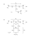
- FIG. 2A and 2B are diagrams showing equivalent circuit diagrams in a single touch state and a multi-touch state, respectively. It is a flowchart of the process in the control circuit of FIG. 4A and 4B are diagrams showing the relationship between the panel current and the dots in the multi-touch state. It is a circuit diagram which shows the structural example of the electric current detection part of FIG.
- FIG. 3 is a circuit diagram showing another configuration example of the control circuit of FIG. 1.
- FIG. 6 is a circuit diagram showing still another configuration example of the control circuit of FIG. 1. It is a figure which shows the relationship between the distance between two points in a multi-touch state, and the detection electric current which flows into a touch panel.
- FIG. 7 is a circuit diagram showing a modification of the control circuit of FIG. 6.
- the state in which the member A is connected to the member B means that the member A and the member B are electrically connected to each other in addition to the case where the member A and the member B are physically directly connected. It includes cases where the connection is indirectly made through other members that do not substantially affect the general connection state, or that do not impair the functions and effects achieved by their combination.
- the state in which the member C is provided between the member A and the member B refers to the case where the member A and the member C or the member B and the member C are directly connected, as well as their electric It includes cases where the connection is indirectly made through other members that do not substantially affect the general connection state, or that do not impair the functions and effects achieved by their combination.
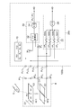
- FIG. 1 is a block diagram illustrating a configuration of an electronic device 1 including a touch panel input device (simply referred to as an input device) 2 according to an embodiment.
- the input device 2 is arranged on the surface layer of an LCD (Liquid Crystal Display) 8, for example, and functions as a touch panel.
- the input device 2 determines an X coordinate and a Y coordinate of a point (point) touched by a user with a finger or a pen (hereinafter referred to as a finger 6).
- the input device 2 includes a touch panel 4 and a control circuit 100.
- the touch panel 4 is a 4-wire (4-terminal) resistive touch panel. Since the configuration of the touch panel 4 is general, it will be briefly described here.
- the touch panel 4 includes a first terminal P1x to a fourth terminal P2y, a first resistance film RF1, and a second resistance film RF2.
- the first resistance film RF1 and the second resistance film RF2 are disposed so as to overlap with a gap in the Z-axis direction perpendicular to the X-axis and the Y-axis.
- One side E1 perpendicular to the X axis of the first resistive film RF1 is connected to the first terminal P1x.
- the side E2 facing the side E1 is connected to the second terminal P2x.
- the third terminal P1y is connected to one side E3 parallel to the X axis of the second resistance film RF2, and the fourth terminal P2y is connected to one side E4 facing the side E3 of the second resistance film RF2.
- the above is the configuration of the touch panel 4.
- the control circuit 100 determines the position of the point touched by the user while switching the first state ⁇ x for detecting the coordinate in the X direction and the second state ⁇ y for detecting the coordinate in the Y direction in a time division manner.
- the control circuit 100 includes a first terminal Pc1x to a fourth terminal Pc2y, a voltage generation unit 10, a voltage detection unit 20, a current detection unit 30, and a calculation unit 40.
- the first terminal Pc1x to the fourth terminal Pc2y are respectively connected to the corresponding first terminal P1x to fourth terminal P2y on the touch panel 4 side.
- the voltage generator 10 applies predetermined first bias voltage Vb1 and second bias voltage Vb2 to the first terminal P1x and the second terminal P2x, respectively.
- the second bias voltage Vb2 is the ground voltage (0V).
- the voltage generator 10 places the third terminal P1y and the fourth terminal P2y in a high impedance state.
- the voltage detector 20 detects the panel voltage VPx generated at the third terminal P1y in the first state ⁇ x.
- the voltage detector 20 includes an A / D converter 24 and converts the detected panel voltage VPx into a digital signal VPx ′.
- the current detection unit 30 detects the panel current IPx flowing in the path including the first terminal P1x, the first resistance film RF1, and the second terminal P2x in the first state ⁇ x.
- the current detection unit 30 includes an I / V conversion unit 32 that converts the panel current IPx into a voltage signal, and an A / D converter 34 that converts the voltage signal into a digital signal VPx ′.
- the calculation unit (coordinate determination unit) 40 determines the X coordinate of the point PU touched by the user based on the values of the panel voltage VPx ′ and the panel current IPx ′.
- the voltage generating unit 10 applies predetermined first bias voltage Vb1 and second bias voltage Vb2 to the third terminal P1y and the fourth terminal P2y, respectively.
- the voltage generation unit 10 places the first terminal P1x and the second terminal P2x in a high impedance state.
- the first bias voltage Vb1 in each of the first state and the second state may be the same value or different. Below, the case of the same value is demonstrated. The same applies to the second bias voltage Vb2.
- the voltage detector 20 detects the panel voltage VPy generated at the first terminal P1x in the second state ⁇ y.
- the A / D converter 24 converts the detected panel voltage VPy into a digital signal VPy ′.
- the voltage detection unit 20 is provided with a two-input selector 22, the first input (0) is connected to the third terminal P1y, and the second input (1) is connected to the first terminal P1x.
- the selector 22 is turned on to the first input (0) side in the first state ⁇ x, and is turned on to the second input (1) side in the second state ⁇ x.
- the voltage detection unit 20 may measure the voltage generated at the fourth terminal P2y as the panel voltage VPx in the first state ⁇ x instead of or in addition to the third terminal P1y. Similarly, in the second state ⁇ y, the voltage detection unit 20 may measure the voltage generated at the second terminal P2x as the panel voltage VPy instead of or in addition to the first terminal P1x.
- the current detection unit 30 detects the panel current IPy flowing in the path including the third terminal P1y, the second resistance film RF2, and the fourth terminal P2y in the second state ⁇ y.
- the I / V converter 32 converts the panel current IPy into a voltage signal
- the A / D converter 34 converts it into a digital value IPy ′.
- the calculation unit (coordinate determination unit) 40 determines the Y coordinate of the point PU touched by the user based on the values of the panel voltage VPy ′ and the panel current IPy ′.
- the third terminal P1y functions as a terminal for detecting the panel voltage VPx in the first state ⁇ x, and functions as a terminal for applying the bias voltage Vb2 to the second resistance film RF2 in the second state ⁇ y.
- the first terminal P1x functions as a terminal for detecting the panel voltage VPy in the second state ⁇ y, and functions as a terminal for applying the bias voltage Vb1 to the first resistance film RF1 in the first state ⁇ x.
- the fourth terminal P2y may be used as a terminal for detecting the panel voltage VPx instead of the third terminal P1y, or the second terminal P1y may be used as a terminal for detecting the panel voltage VPy instead of the first terminal P1x. Also good.
- control circuit 100 The above is the overall configuration of the control circuit 100. Next, the principle of coordinate detection by the control circuit 100 will be described. Here, the principle of detecting the X coordinate in the first state ⁇ x will be described, but the same applies to the Y coordinate.
- FIGS. 2A and 2B show equivalent circuit diagrams in a single touch state and a multi-touch state, respectively. Each resistance shown in the equivalent circuit actually occurs as a distributed constant, but is shown here as an individual resistance element for the sake of simplicity.
- the first resistive film RF1 is divided resistor R1 1 between the first terminal P1x and point PU, the resistance R1 2 between points PU and the second terminal P2x.
- the first resistance film RF1 and the second resistance film RF2 are in contact at a point PU, and the contact resistance is Rc.
- the resistance of the path from the point PU of the second resistance film RF2 to the third terminal P1y is R2.
- the potential of the point PU since those obtained by dividing the bias voltage Vb1 and Vb2 at the resistor R1 1, R1 2, shows the X-coordinate of the point PU.
- the potential of PU is substantially equal to the voltage of the third terminal P1y. That is, the panel voltage VPx generated at the third terminal P1y indicates the X coordinate of the point PU.
- the algorithm for deriving the X coordinate from the panel voltage VPx may be a known technique and is not particularly limited in the present invention.
- the impedance in the non-contact state and the single touch state is not particularly distinguished and is referred to as a reference impedance Zo.
- This panel current IPxo is referred to as a reference panel current.
- the first resistive film RF1 includes a resistor R1 1 between the first terminal P1x and the point PU1, the resistor R1 2 between the points PU1 and the point PU2, the point PU2 second It is divided into the resistor R1 3 between the terminals P2x.
- the first resistance film RF1 and the second resistance film RF2 are in contact at points PU1 and PU2, and the respective contact resistances are Rc 1 and Rc 2 .
- the resistance between the points PU1 and PU2 are R2 1
- resistance of a path from the point PU1 reach the third terminal P1y is R2 2
- the path from the point PU2 reach the third terminal P1y
- the resistance of R2 is 3 .
- the panel current IPx in the multi-touch state is determined by the combined impedance Zm between the first terminal P1x and the second terminal P2x.
- This combined impedance Zm and the impedance Zo in a non-contact state or a single touch state are Zm ⁇ Zo Holds.
- the multi-touch state and the single touch state can be distinguished by monitoring the panel current IPx and comparing it with the reference panel current IPxo.
- the potentials of the points PU1 and PU2 are obtained by dividing the bias voltages Vb1 and Vb2 by the resistors R1 1 , R1 2 , R1 3 and other resistance components, they have a correlation with the respective X coordinates of the points PU1 and PU2. Since the panel voltage VPx generated at the third terminal P1y is also correlated with the two points PU1 and PU2, if the multi-touch state is known, the points PU1 and PU2 are based on the panel voltage VPx. Can be estimated.
- one X coordinate X3 determined by the same algorithm as in the single touch state indicates the coordinate of any point between the points PU1 and PU2 touched by the user.
- the panel current IPx is monitored and processed in combination so that the user in the multi-touch state as well as the single touch is processed.
- the coordinates of the contact point can be determined.
- the calculation unit 40 includes a multi-touch determination unit 42, a distance calculation unit 44, a table 46, and a coordinate generation unit 48.
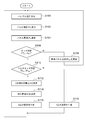
- FIG. 3 is a flowchart of processing in the control circuit 100 of FIG. The flow of FIG. 3 shows the first state ⁇ x for determining the X coordinate. Each step can be exchanged within a range that does not hinder the processing, or some steps may be processed simultaneously in parallel.
- the bias voltages Vb1 and Vb2 are applied to the first terminal P1x and the second terminal P2x by the voltage generator 10 (S100).
- the voltage detector 20 measures the panel voltage VPx (S102)
- the current detector 30 measures the panel current IPx (S104).
- the calculation unit 40 receives the digital values VPx ′ and IPx ′ corresponding to the panel voltage VPx and the panel current IPx thus obtained.
- the coordinate generation unit 48 determines the presence or absence of a touch by comparing the panel voltage VPx with a predetermined threshold voltage Vth.
- the threshold voltage Vth is set to a value near 0V.
- the multi-touch determination unit 42 determines that it is a single touch, and notifies the coordinate generation unit 48 of the determination result.
- the coordinate generation unit 48 determines the X coordinate based on the panel voltage VPx (S118).
- the multi-touch determination unit 42 determines multi-touch when IPx> IPxo (Y in S110), and notifies the distance calculation unit 44 and the coordinate generation unit 48 of the determination result.
- the distance calculation unit 44 determines the distance ⁇ X between the two points PU1 and PU2 (S112).
- the present inventor has come to recognize that there is a correlation between the distance ⁇ X between the two points PU1 and PU2 and the panel current IPx. That is, when the distance ⁇ X between the two points is zero, the panel current IPx is almost the same as the reference current IPxo because it is the same as the single touch.
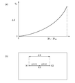
- 4A and 4B are diagrams showing the relationship between the panel current and the dots in the multi-touch state.
- the panel current IPx becomes the minimum value IPxmin.
- FIG. 4A shows the relationship between the differential current (IPx ⁇ IPxo) and the distance ⁇ X.
- the characteristics shown in FIG. 4A may be measured in advance for each touch panel 4 or may be derived by simulation.
- the table 46 stores the relationship between the differential current (IPx ⁇ IPxo) and the distance ⁇ X.
- the distance calculation unit 44 determines the corresponding distance ⁇ X by referring to the table 46 based on the panel current IPx, and outputs it to the coordinate generation unit 48. Instead of the table 46, an approximate expression of the characteristic shown in FIG. 4A may be stored, and the distance ⁇ X may be calculated by calculation.
- the coordinate generator 48 receives data indicating the distance ⁇ X and the panel voltage VPx.
- the coordinate generation unit 48 calculates the X coordinate X3 corresponding to the panel voltage VPx using an algorithm similar to that for single touch or an algorithm different from that. Then, the X coordinate X3 is set as the center coordinates of two points (S114).
- the coordinate generation unit 48 determines one coordinate PU2 of the two points by adding a value (half here) ⁇ X / 2 corresponding to the coordinate interval ⁇ X of the two points to the center coordinate X3, and 2 from the center coordinates X3 By subtracting the value ⁇ X / 2 corresponding to the coordinate interval ⁇ X of the points, the other coordinate PU1 of the two points is determined (S116).
- FIG. 4B shows this process. Then, it returns to step S100.
- step S106 when VPx ⁇ Vth (N in S106), the coordinate generation unit 48 determines that it is in a non-contact state. Subsequently, in step S104, the multi-touch determination unit 42 updates the reference panel current IPxo using the measured panel current IPx (S108). Then, it returns to step S100.
- control circuit 100 The above is a specific processing flow by the control circuit 100.
- the input device 2 can suitably discriminate between single touch and multi-touch, and can generate the coordinates of points in each state. Furthermore, the input device 2 according to the embodiment has the following advantages.
- step S108 by updating the reference panel current IPxo, it is possible to reduce the influence of aging deterioration and temperature fluctuation of the touch panel 4. That is, when the values of the first resistance film RF1, the second resistance film RF2, and their contact resistance change according to deterioration and temperature fluctuation, the reference current IPxo changes accordingly. Therefore, if the reference current IPxo is used in a fixed manner, it may cause erroneous detection of multi-touch, or an error may occur in the distance ⁇ X between two points. On the other hand, such a problem can be suitably solved by updating the reference current IPxo during the process.
- the differential current (IPx ⁇ IPxo) when determining the distance ⁇ X between the two points in the multi-touch state has the following merits. As described above, since the impedance of the panel changes with time or with temperature fluctuation, the value of the panel current IPx when the same coordinate is touched also changes. Therefore, if the differential current is calculated, the influence of aging deterioration and temperature fluctuation can be reduced, and accurate coordinate detection becomes possible.
- FIG. 5 is a circuit diagram showing a configuration example of the current detection unit 30 of FIG.
- the current detection unit 30 includes detection resistors Rsx and Rsy, bypass switches SW1x and SW1y, a selector 36, and an A / D converter 34.
- the detection resistors Rsx and Rsy correspond to the I / V conversion unit 32 in FIG.
- the detection resistor Rsx and the bypass switch SW1x are used for coordinate detection in the X-axis direction, and the detection resistor Rsy and the bypass switch SW1y are used for coordinate detection in the Y-axis direction. Since the X axis and the Y axis are configured in the same manner, the X axis direction will be described here.
- the detection resistor Rsx is provided on an extension of a path including the first terminal P1x, the first resistance film RF1, and the second terminal P2x. Specifically, one end of the detection resistor Rsx is grounded and the potential is fixed, and the other end is connected to the second terminal Pc2x.
- the bypass switch SW1x is provided in parallel with the corresponding detection resistor Rsx. Specifically, one end of the bypass switch SW1x is grounded, and the other end is connected to the second terminal Pc2x.
- the bypass switch SWx When the voltage detector 20 detects the panel voltage VPx, the bypass switch SWx is turned on. At this time, since the detection resistor Rs does not affect the combined impedance of the touch panel 4, an accurate panel voltage VPx can be measured.
- the bypass switch SWx When the panel current IPx is detected by the current detector 30, the bypass switch SWx is turned off. Then, a voltage drop (Rsx ⁇ IPx) proportional to the panel current IPx occurs in the detection resistor Rsx.
- the selector 36 is turned on to the terminal (0) side when detecting coordinates in the X-axis direction, and is turned on to the terminal (1) side when detecting coordinates in the Y-axis direction.
- the voltage drop of the detection resistor Rsx is converted into a digital value by the A / D converter 34. This digital value takes a value corresponding to the panel current IPx.
- the bypass switch SW1x can function as the voltage generation unit 10. That is, when the second bias voltage Vb2 is applied to the second terminal P2x, the bypass switch SW1x may be turned on. The same applies to the bypass switch SW1y.
- FIG. 6 is a circuit diagram showing another configuration example of a part of the control circuit of FIG.
- the voltage generator 10a of the control circuit 100a includes a regulator 11, a first selector SEL1, and a second selector SEL2.
- the regulator 11 and the first selector SEL1 generate the first bias voltage Vb1 and apply it to the first terminal P1x in the first state ⁇ x and to the third terminal P1y in the second state ⁇ y.
- the regulator 11 generates a first bias voltage Vb1 corresponding to the reference voltage Vref. Since the regulator 11 is a general linear regulator including an operational amplifier 12, an output transistor 14, a first resistor R1, and a second resistor R2, description of the configuration and operation is omitted.
- the value of the reference voltage Vref may be switched between the first state ⁇ x and the second state ⁇ y.
- the first selector SEL1 receives the first bias voltage Vb1 at its input terminal.
- the first output terminal (0) of the first selector SEL1 is connected to the first terminal Pc1x, and the second output terminal (1) is connected to the third terminal Pc1y.
- the first selector SEL1 is turned on to the first output terminal (0) side in the first state ⁇ x, and is turned on to the second output terminal (1) side in the second state ⁇ y.
- the first selector SEL1 includes switches SWa1 and SWa2 that are turned on and off in a complementary manner.
- the second selector SEL2 is provided to apply the second bias voltage Vb2 to the touch panel 4.
- the second bias voltage Vb2 is a ground voltage
- the second selector SEL2 includes switches SWb1 and SWb2 that are turned on and off in a complementary manner.
- the switch SWb1 is turned on in the first state ⁇ x
- the switch SWb2 is turned on in the second state ⁇ y.
- the current detection unit 30a includes a detection transistor 38, a detection resistor Rs, and an A / D converter 34.
- the detection transistor 38 is connected to the output transistor 14 of the regulator 11 so as to form a current mirror circuit.
- a current flowing through the output transistor 14, that is, a detection current Is proportional to the panel current flows through the detection transistor 38.
- Is K1 ⁇ IP Holds.
- the detection resistor Rs is provided on the path of the detection transistor Rs.
- a voltage drop Vs proportional to the detection current Is occurs in the detection transistor Rs, which is proportional to the panel current IP.
- the A / D converter 34 converts the voltage drop Vs generated in the detection resistor Rs into a digital value and outputs it as signals IPx ′ and IPy ′ indicating the panel current IP.
- the control circuit 100a in FIG. 6 has the following advantages over the control circuit using the current detection unit 30 in FIG. 6
- the panel current IP can be detected without affecting the panel voltage VP.
- the bypass switch SW1x (or SW1y) is turned on to measure the panel voltage VPx (or VPy), and the bypass switch SW1x (or SW1y) is turned off to turn on the panel. It is necessary to switch the state of measuring the current IPx (or IPy), and coordinate detection may take time. In addition, since the corresponding panel voltage VPx and the panel current IPx (or VPy and IPy) are measured at different timings, the coordinate measurement accuracy deteriorates. On the other hand, the control circuit 100a of FIG. 6 can measure the panel voltage and the panel current simultaneously in parallel, so that the processing can be speeded up and is suitable for an application that requires high speed. Further, since two parameters necessary for determining the coordinates, that is, voltage and current can be acquired simultaneously, the coordinates can be determined with high accuracy.
- the difference ⁇ I between the panel current when touching at one point and the panel current when touching at two points may be very small depending on the panel.
- the change amount ⁇ V of the voltage drop Vs of the detection resistor Rs can be sufficiently secured, and the accuracy required for the A / D converter 34 is improved. Can be lowered.
- the current detection unit 30a may switch the mirror ratio K1 between the output transistor 14 and the detection transistor 38 in the first state ⁇ x and the second state ⁇ y.
- the detection resistor Rs is a variable resistor, and instead of or in addition to switching the mirror ratio, the current detection unit 30a may switch the resistance value of the detection resistor Rs in the first state ⁇ x and the second state ⁇ y.
- the combined resistance in the vertical direction is different from the combined resistance in the horizontal direction, the range of the panel current IPx in the X direction, and the panel current in the Y direction. It is assumed that the IPy range is different.
- the voltage range of the voltage drop Vs of the detection resistor Rs can be made uniform by switching the values of the mirror ratio K1 and the detection resistor Rs between the first state ⁇ x and the second state ⁇ y.
- the converter 34 can perform processing with high accuracy.
- the output transistor 14 and the detection transistor 38 in FIG. 6 form a current mirror circuit, this may be a cascode type current mirror circuit. In this case, the accuracy of replicating the current, that is, the accuracy of the mirror ratio can be increased.
- FIG. 7 is a circuit diagram showing a modification of the control circuit of FIG.
- the control circuit 100b of FIG. 7 is different from that of FIG. 1 in the processing of the panel voltage VP. 1 detects the panel voltage VPx generated at the third terminal P1y in the first state ⁇ x, and detects the panel voltage VPy generated at the first terminal P1x in the second state ⁇ y.
- Voltage detection unit 20b includes switches SW4 to SW7 and A / D converter 24.
- the switches SW4 to SW7 correspond to the selector 22 in FIG.
- the switch SW4 is first turned on and the rest is turned off.
- the panel voltage VPx_1 at the third terminal P1y is measured.
- the switch SW5 is turned on and the rest is turned off.
- the panel voltage VPx_2 at the fourth terminal P2y is measured.
- a subsequent calculation unit 40 determines the X coordinate of the point PU touched by the user based on the values of the two panel voltages VPx_1 and VPx_2 and the panel current IPx.
- the switch SW6 is first turned on and the rest is turned off.
- the panel voltage VPy_1 at the first terminal P1x is measured.
- the switch SW7 is turned on and the rest is turned off.
- the panel voltage VPy_2 at the second terminal P2x is measured.
- a calculation unit 40 (not shown) in the subsequent stage determines the Y coordinate of the point PU touched by the user based on the values of the two panel voltages VPy_1 and VPy_2 and the panel current IPy.
- the panel voltage at the two terminals can be measured in each of the first state ⁇ x and the second state ⁇ y and reflected in the determination of the X coordinate and the Y coordinate, thereby improving the coordinate detection accuracy. it can.
- the characteristics of the touch panel 4 to be controlled by the control circuit 100 are various.
- the contact resistance between the first resistance film RF1 and the second resistance film RF2 of the touch panel 4 varies greatly depending on the type of the touch panel 4.
- the inexpensive touch panel 4 tends to have a high contact resistance.
- the low touch resistance is several hundred ⁇ or less, whereas the low touch resistance is several tens of k ⁇ .
- FIG. 8 is a diagram illustrating the relationship between the distance ⁇ X between two points in the multi-touch state and the detected current Ip flowing through the touch panel 4.
- (I) shows the case where the contact resistance is small
- (II) shows the case where the contact resistance is large.
- the degree of contribution of the resistance component of the second resistive film RF2 to the combined resistance between the terminals P1 X and P2 X by multi-touch is small in the contact resistances Rc 1 and Rc 2. The higher it gets. Therefore, in a panel having a large contact resistance, the panel current Ip that flows when multi-touch is performed is small. That is, since the change in the panel current Ip with respect to the change in the distance ⁇ X between the two points becomes small, it becomes difficult to detect the distance ⁇ X between the two points.
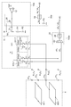
- FIG. 9 is a circuit diagram showing a modification of the control circuit of FIG.
- the control circuit 100c of FIG. 9 includes an amplifier circuit 50, a switch SW8, and a buffer 60 in addition to the configuration of FIG.
- the amplifier circuit 50 is provided in the current detection unit 30c.
- the amplifier circuit 50 amplifies the difference between the voltage drop (detection voltage) Vs generated in the detection resistor Rs and a predetermined offset voltage V OFS with a gain A, and outputs the amplified voltage value V_Ip indicating the panel current Ip.
- V_Ip A ⁇ (Vs ⁇ V OFS ) (1)
- the amplifier circuit 50 includes a buffer 52, an operational amplifier 54, a first resistor R11 to a fourth resistor R14, and a voltage source (D / A converter) 56.
- the voltage source 56 generates a predetermined voltage Va corresponding to the input digital value.
- the buffer 52 is a voltage follower that receives the detection voltage Vs generated in the detection resistor Rs.
- the first resistor R11 is provided between the output of the buffer 52 and the first input terminal of the operational amplifier 54.
- the second resistor R12 is provided between the first input terminal of the operational amplifier 54 and a fixed voltage terminal (ground terminal).
- the third resistor R13 receives a predetermined voltage Va at one end, and the other end is connected to the second input terminal of the operational amplifier 54.
- the fourth resistor R14 is provided between the second input terminal of the operational amplifier 54 and the output terminal of the operational amplifier 54.
- gain A and offset voltage V OFS are given by equations (2) and (3), respectively.
- A R12 ⁇ (R13 + R14) / (R13 ⁇ (R11 + R12)) (2)
- V OFS R14 ⁇ (R11 + R12) / (R12 ⁇ (R13 + R14)) ⁇ Va (3)
- the current detection unit 30 c includes a buffer 60 provided in the preceding stage of the A / D converter 24.
- the buffer 60 is a voltage follower that receives the panel voltage VP via the selector 22.
- the A / D converter 24 samples and holds the output voltage VX of the buffer 60, and converts the sampled and held value into a digital value.
- a switch and a capacitor are provided at the input stage of the A / D converter 24.
- the switch SW8 is provided between the input and output of the amplifier circuit 50. In the on state of the switch SW8, the amplifier circuit 50 is bypassed.
- the resistance value of the detection resistor Rs is optimized according to the resistance value of the touch panel 4, in other words, according to the panel current IP. Thereby, the range of the detection voltage Vs is optimized.
- the voltage Va that is, the offset voltage V OFS is optimized.
- Va 0 may be set.
- the A / D converter 34 measures the voltage value V_Ip of Expression (6).
- V_Ip R2 / R1 ⁇ V init ... (6)
- the current change amount ⁇ I due to the contact with the user decreases as the contact resistance increases.
- the voltage change amount ⁇ V corresponding to the current change amount ⁇ I is amplified by the amplifier circuit 50, so that the distance ⁇ X between the two points can be detected more accurately even in the touch panel 4 having a large contact resistance. can do.
- the capacitor at the input stage of the A / D converter 24 is charged via the resistance component of the touch panel 4. Therefore, when the contact resistance is large, the charging speed is slowed down and the time required for the sample hold is lengthened. When the sample hold time becomes longer, the response speed of coordinate detection becomes slower.
- the charging speed can be increased by providing the buffer 60 having a small output impedance.
- the sample hold time can be shortened, and as a result, the response speed of coordinate detection can be increased.
- the coordinate generation unit 48 estimates the coordinate X3 corresponding to the panel voltage VPx to be the midpoint between the two points PU1 and PU2, and determines the original coordinates X1 and X2.
- the present invention is not limited to this, and more complicated algorithms may be used.
- a part of the control circuit 100 in FIG. 1 is shared in the first state ⁇ x and the second state ⁇ y, but may be provided completely separately. Further, the present invention may be applied to only one of the X direction and the Y direction only.
- SYMBOLS 1 Electronic device, P1x ... 1st terminal, P1y ... 3rd terminal, RF1 ... 1st resistance film, Pc1 ... 1st terminal, SW1 ... Bypass switch, R1 ... 1st resistance, SEL1 ... 1st selector, 2 ... Input Device, P2x ... second terminal, P2y ... fourth terminal, RF2 ... second resistive film, Pc2 ... second terminal, R2 ... second resistor, SEL2 ... second selector, 4 ... touch panel, 6 ... finger, 8 ... LCD DESCRIPTION OF SYMBOLS 10 ... Voltage generation part, 11 ... Regulator, 12 ...
- the present invention can be used for an input device of an electronic device.
Landscapes
- Engineering & Computer Science (AREA)
- General Engineering & Computer Science (AREA)
- Theoretical Computer Science (AREA)
- Human Computer Interaction (AREA)
- Physics & Mathematics (AREA)
- General Physics & Mathematics (AREA)
- Position Input By Displaying (AREA)
- User Interface Of Digital Computer (AREA)
Abstract
電圧生成部10aは、第1端子P1x、第1抵抗膜RF1、第2端子P2xを含む経路の第1端子P1x側の延長上に設けられた出力トランジスタ14を有し、第1端子P1xに第1バイアス電圧Vb1を印加する。電流検出部30aは、出力トランジスタ14とカレントミラー形式で接続された検出トランジスタ38と、検出トランジスタ38の経路上に設けられた検出抵抗Rsと、検出抵抗Rsの電圧降下Vsと所定の電圧VOFSとの差分を増幅し、パネル電流Ipを示す値として出力する増幅回路50と、を含む。
Description
本発明は、抵抗膜方式タッチパネルに関し、特に複数の点の同時接触(マルチタッチ)を検出する技術に関する。
近年のコンピュータや携帯電話端末、PDA(Personal Digital Assistant)などの電子機器は、指で接触することによって電子機器を操作するための入力装置を備えるものが主流となっている。こうした入力装置として、抵抗膜式のタッチパネル(タッチセンサ)などが知られている(特許文献1)。
近年、マルチタッチに対応したタッチパネルが要求されているが、それは静電センサ型のタッチパネルでのみ実現されており、抵抗膜方式のタッチパネルでは実現されていない。なぜなら抵抗膜方式のタッチパネルにおいては、パネルから出力される電圧にもとづいてユーザがタッチした位置(座標)が決定されるところ、2点をタッチした場合(マルチタッチ)のパネルの出力電圧と、1点をタッチした場合(シングルタッチ)のパネルの出力電圧を区別することができないからである。
特許文献1には、マルチタッチの検出が可能なタッチパネル入力装置が開示されているが、マルチタッチを誤入力として扱っており、積極的にマルチタッチを有効な入力としては扱っておらず、したがってマルチタッチにともなう複数の点の座標を特定する技術は開示されていない。
本発明は係る課題に鑑みてなされたものであり、そのある態様の例示的な目的のひとつは、マルチタッチに対応可能なタッチパネルの制御技術の提供にある。
本発明のある態様は、タッチパネルの制御回路に関する。タッチパネルは、第1、第2、第3端子と、一辺が第1端子と接続され、それと対向する辺が第2端子と接続される第1抵抗膜と、第1抵抗膜とギャップを隔てて配置され、その一辺が第3端子と接続される第2抵抗膜と、を有する。制御回路は、第1、第2端子それぞれに所定の第1、第2バイアス電圧を印加する電圧生成部と、第3端子に生ずるパネル電圧を検出する電圧検出部と、第1端子、第1抵抗膜、第2端子を含む経路に流れるパネル電流を検出する電流検出部と、パネル電圧およびパネル電流の値にもとづき、ユーザが接触した座標を判定する座標判定部と、を備える。電圧生成部は、第1端子、第1抵抗膜、第2端子を含む経路の第1端子側の延長上に設けられた出力トランジスタを有し、第1端子に第1バイアス電圧を印加するレギュレータを含む。電流検出部は、出力トランジスタとカレントミラー回路を形成するように接続された検出トランジスタと、当該検出トランジスタの経路上に設けられた検出抵抗と、検出抵抗の電圧降下と所定の電圧との差分を増幅し、パネル電流を示す値として出力する増幅回路と、を含む。
ユーザがタッチパネルの複数の点にタッチすると、第1端子から第2端子に至る経路の合成抵抗値が減少し、それに応じたパネル電流が変化する。この態様によると、パネル電流をモニタすることにより、マルチタッチを好適に検出でき、さらに複数点の座標を決定することができる。また、パネル電流を検出するための検出抵抗が、第1端子、第1抵抗膜、第2端子を含む経路ではなく、それとは別の経路に設けられているため、パネル電圧に影響を与えることなく、パネル電流を検出できる。また所定の電圧を最適化することにより、増幅回路の出力電圧は、タッチパネルの接触に応じたパネル電流の変化量に比例した値となる。そしてタッチパネルの第1抵抗膜と第2抵抗膜の接触抵抗が大きい場合にも、マルチタッチを検出できる。
本発明の別の態様もまた、制御回路である。この制御回路は、第1状態において第1、第2端子それぞれに所定の第1、第2バイアス電圧を印加し、第3、第4端子をハイインピーダンス状態とし、第2状態において第3、第4端子それぞれに所定の第1、第2バイアス電圧を印加し、第1、第2端子をハイインピーダンス状態とする電圧生成部と、第1状態において、第3、第4端子の一方に生ずるパネル電圧を検出し、第2状態において、第1、第2端子の一方に生ずるパネル電圧を検出する電圧検出部と、第1状態において、第1端子、第1抵抗膜、第2端子を含む経路に流れるパネル電流を検出し、第2状態において、第3端子、第2抵抗膜、第4端子を含む経路に流れるパネル電流を検出する電流検出部と、パネル電圧およびパネル電流の値にもとづき、ユーザが接触した座標を判定する座標判定部と、を備える。電圧生成部は、出力トランジスタを有し、第1バイアス電圧を生成するレギュレータと、その入力端子に第1バイアス電圧を受け、その第1出力端子に第1端子が接続され、その第2出力端子に第3端子が接続され、第1状態において第1出力端子側にオンし、第2状態において第2出力端子側にオンするセレクタと、を含む。電流検出部は、出力トランジスタとカレントミラー回路を形成するように接続された検出トランジスタと、当該検出トランジスタの経路上に設けられた検出抵抗と、検出抵抗の電圧降下と所定の電圧との差分を増幅し、パネル電流を示す値として出力する増幅回路と、を含む。
この態様によると、X方向とY方向の両方についてマルチタッチおよび複数点の座標を決定できる。また、パネル電流を検出するための検出抵抗が、タッチパネルに直接接続されていないため、パネル電圧に影響を与えることなく、パネル電流を検出できる。また所定の電圧を最適化することにより、増幅回路の出力電圧は、タッチパネルの接触に応じたパネル電流の変化量に比例した値となる。そしてタッチパネルの第1抵抗膜と第2抵抗膜の接触抵抗が大きい場合にも、マルチタッチを検出できる。
本発明のさらに別の態様もまた、制御回路である。この制御回路は、第1状態において第1、第2端子それぞれに所定の第1、第2バイアス電圧を印加し、第3、第4端子をハイインピーダンス状態とし、第2状態において第3、第4端子それぞれに所定の第1、第2バイアス電圧を印加し、第1、第2端子をハイインピーダンス状態とする電圧生成部と、第1状態において、第3、第4端子それぞれに生ずるパネル電圧を個別に検出し、第2状態において、第1、第2端子それぞれに生ずるパネル電圧を個別に検出する電圧検出部と、第1状態において、第1端子、第1抵抗膜、第2端子を含む経路に流れるパネル電流を検出し、第2状態において、第3端子、第2抵抗膜、第4端子を含む経路に流れるパネル電流を検出する電流検出部と、パネル電圧およびパネル電流の値にもとづき、ユーザが接触した座標を判定する座標判定部と、を備える。電圧生成部は、出力トランジスタを有し、第1バイアス電圧を生成するレギュレータと、その入力端子に第1バイアス電圧を受け、その第1出力端子に第1端子が接続され、その第2出力端子に第3端子が接続され、第1状態において第1出力端子側にオンし、第2状態において第2出力端子側にオンするセレクタと、を含む。電流検出部は、出力トランジスタとカレントミラー回路を形成するように接続された検出トランジスタと、当該検出トランジスタの経路上に設けられた検出抵抗と、検出抵抗の電圧降下と所定の電圧との差分を増幅し、パネル電流を示す値として出力する増幅回路と、を含む。
増幅回路は、検出抵抗の電圧降下を受けるバッファと、演算増幅器と、バッファの出力と演算増幅器の第1入力端子との間に設けられた第1抵抗と、演算増幅器の第1入力端子と固定電圧端子の間に設けられた第2抵抗と、その一端に所定の電圧を受け、その他端が演算増幅器の第2入力端子と接続された第3抵抗と、演算増幅器の第2入力端子と演算増幅器の出力端子の間に設けられた第4抵抗と、を含んでもよい。
電圧検出部は、パネル電圧を受けるバッファと、バッファの出力電圧をサンプルホールドし、サンプルホールドした値をデジタル値に変換するA/Dコンバータと、を含んでもよい。
バッファを設けない場合、A/Dコンバータの入力段のキャパシタがパネルの接触抵抗を介して充電されることになり、パネルの接触抵抗が大きいとサンプルホールドに要する時間が長くなる。そこで出力インピーダンスの小さなバッファを設けることにより、パネルの接触抵抗にかかわらず、サンプルホールド時間を短縮できる。
バッファを設けない場合、A/Dコンバータの入力段のキャパシタがパネルの接触抵抗を介して充電されることになり、パネルの接触抵抗が大きいとサンプルホールドに要する時間が長くなる。そこで出力インピーダンスの小さなバッファを設けることにより、パネルの接触抵抗にかかわらず、サンプルホールド時間を短縮できる。
電流検出部は、第1状態と第2状態において、出力トランジスタと検出トランジスタのミラー比を切りかえ可能に構成されてもよい。
電流検出部は、第1状態と第2状態において、検出抵抗の抵抗値を切りかえ可能に構成されてもよい。
タッチパネルの縦の長さと横の長さ(つまりアスペクト比)が大きく異なる場合、縦方向の合成抵抗と横方向の合成抵抗が異なり、パネル電流のレンジがX方向とY方向とで異なる場合が想定される。この場合に、ミラー比や検出抵抗の値を切りかえることにより、検出抵抗の電圧降下の範囲を揃えることができる。
電流検出部は、第1状態と第2状態において、検出抵抗の抵抗値を切りかえ可能に構成されてもよい。
タッチパネルの縦の長さと横の長さ(つまりアスペクト比)が大きく異なる場合、縦方向の合成抵抗と横方向の合成抵抗が異なり、パネル電流のレンジがX方向とY方向とで異なる場合が想定される。この場合に、ミラー比や検出抵抗の値を切りかえることにより、検出抵抗の電圧降下の範囲を揃えることができる。
座標判定部は、パネル電流の値が所定の値より大きいとき、ユーザが複数の点を接触しているものと判定してもよい。
ユーザが2点に接触しているとき、パネル電流の値にもとづいて2点の座標間隔を決定してもよい。パネル電流が大きいほど、2点の座標間隔が大きいと判定してもよい。
ユーザが2点に接触すると、その2点の間は、第1抵抗膜と第2抵抗膜が並列に接続されるため、第1から第2端子に至る経路の合成抵抗が低下し、したがってパネル電流が増大する。2点の距離が離れるほど、第1抵抗膜と第2抵抗膜が並列に接続される距離が長くなるため、合成抵抗は小さくなり、パネル電流は大きくなる。したがって、パネル電流にもとづいて2点の座標間隔を決定することができる。
ユーザが2点に接触すると、その2点の間は、第1抵抗膜と第2抵抗膜が並列に接続されるため、第1から第2端子に至る経路の合成抵抗が低下し、したがってパネル電流が増大する。2点の距離が離れるほど、第1抵抗膜と第2抵抗膜が並列に接続される距離が長くなるため、合成抵抗は小さくなり、パネル電流は大きくなる。したがって、パネル電流にもとづいて2点の座標間隔を決定することができる。
ユーザがパネルに接触していないときに測定されたパネル電流と、接触したときのパネル電流の差分にもとづいて、2点の座標間隔を決定してもよい。
座標判定部は、パネル電圧にもとづいて2点の中心座標を決定し、当該中心座標に2点の座標間隔に応じた値を加算することで、2点の一方の座標を決定し、中心座標から2点の座標間隔に応じた値を減算することで、2点の他方の座標を決定してもよい。
本発明のさらに別の態様は、タッチパネル入力装置である。この入力装置は、タッチパネルと、タッチパネルを制御する上述のいずれかの制御回路と、を備える。
本発明のさらに別の態様は、電子機器である。この電子機器は、上述のタッチパネル入力装置を備える。
なお、以上の構成要素を任意に組み合わせたもの、あるいは本発明の表現を、方法、装置などの間で変換したものもまた、本発明の態様として有効である。
本発明のある態様によれば、接触抵抗が大きなタッチパネルについても、マルチタッチ入力を正確に検出できる。
以下、本発明を好適な実施の形態をもとに図面を参照しながら説明する。各図面に示される同一または同等の構成要素、部材、処理には、同一の符号を付するものとし、適宜重複した説明は省略する。また、実施の形態は、発明を限定するものではなく例示であって、実施の形態に記述されるすべての特徴やその組み合わせは、必ずしも発明の本質的なものであるとは限らない。
本明細書において、「部材Aが、部材Bと接続された状態」とは、部材Aと部材Bが物理的に直接的に接続される場合のほか、部材Aと部材Bが、それらの電気的な接続状態に実質的な影響を及ぼさない、あるいはそれらの結合により奏される機能や効果を損なわせない、その他の部材を介して間接的に接続される場合も含む。
同様に、「部材Cが、部材Aと部材Bの間に設けられた状態」とは、部材Aと部材C、あるいは部材Bと部材Cが直接的に接続される場合のほか、それらの電気的な接続状態に実質的な影響を及ぼさない、あるいはそれらの結合により奏される機能や効果を損なわせない、その他の部材を介して間接的に接続される場合も含む。
同様に、「部材Cが、部材Aと部材Bの間に設けられた状態」とは、部材Aと部材C、あるいは部材Bと部材Cが直接的に接続される場合のほか、それらの電気的な接続状態に実質的な影響を及ぼさない、あるいはそれらの結合により奏される機能や効果を損なわせない、その他の部材を介して間接的に接続される場合も含む。
図1は、実施の形態に係るタッチパネル入力装置(単に入力装置という)2を備える電子機器1の構成を示すブロック図である。入力装置2は、たとえばLCD(Liquid Crystal Display)8の表層に配置され、タッチパネルとして機能する。入力装置2は、ユーザが指やペンなど(以下、指6)でタッチしたポイント(点)のX座標およびY座標を判定する。
入力装置2は、タッチパネル4、制御回路100を備える。タッチパネル4は4線式(4端子)の抵抗膜方式タッチパネルである。タッチパネル4の構成は一般的なものであるためここでは簡単に説明する。
タッチパネル4は、第1端子P1x~第4端子P2y、第1抵抗膜RF1、第2抵抗膜RF2を備える。
第1抵抗膜RF1および第2抵抗膜RF2は、X軸およびY軸に対して垂直なZ軸方向にギャップを隔ててオーバーラップして配置される。第1抵抗膜RF1のX軸と垂直な一辺E1は、第1端子P1xと接続される。辺E1と対向する辺E2は、第2端子P2xと接続される。第3端子P1yは、第2抵抗膜RF2のX軸と平行な一辺E3と接続され、第4端子P2yは、第2抵抗膜RF2の辺E3と対向する一辺E4と接続される。
以上がタッチパネル4の構成である。
第1抵抗膜RF1および第2抵抗膜RF2は、X軸およびY軸に対して垂直なZ軸方向にギャップを隔ててオーバーラップして配置される。第1抵抗膜RF1のX軸と垂直な一辺E1は、第1端子P1xと接続される。辺E1と対向する辺E2は、第2端子P2xと接続される。第3端子P1yは、第2抵抗膜RF2のX軸と平行な一辺E3と接続され、第4端子P2yは、第2抵抗膜RF2の辺E3と対向する一辺E4と接続される。
以上がタッチパネル4の構成である。
制御回路100は、X方向の座標を検出する第1状態φxと、Y方向の座標を検出する第2状態φyを時分割的にスイッチしながら、ユーザが接触した点の位置を判定する。
制御回路100は、第1端子Pc1x~第4端子Pc2y、電圧生成部10、電圧検出部20、電流検出部30、演算部40を備える。
第1端子Pc1x~第4端子Pc2yはそれぞれ、タッチパネル4側の対応する第1端子P1x~第4端子P2yと接続される。
第1端子Pc1x~第4端子Pc2yはそれぞれ、タッチパネル4側の対応する第1端子P1x~第4端子P2yと接続される。
はじめに、X方向の座標(X座標)を検出するための構成を説明する。
電圧生成部10は、第1状態φxにおいて、第1端子P1x、第2端子P2xそれぞれに所定の第1バイアス電圧Vb1、第2バイアス電圧Vb2を印加する。ここではVb1>Vb2とする。好ましくは第2バイアス電圧Vb2は接地電圧(0V)である。また第1状態において、電圧生成部10は第3端子P1y、第4端子P2yをハイインピーダンス状態とする。
電圧生成部10は、第1状態φxにおいて、第1端子P1x、第2端子P2xそれぞれに所定の第1バイアス電圧Vb1、第2バイアス電圧Vb2を印加する。ここではVb1>Vb2とする。好ましくは第2バイアス電圧Vb2は接地電圧(0V)である。また第1状態において、電圧生成部10は第3端子P1y、第4端子P2yをハイインピーダンス状態とする。
電圧検出部20は、第1状態φxにおいて第3端子P1yに生ずるパネル電圧VPxを検出する。電圧検出部20は、A/Dコンバータ24を含み、検出したパネル電圧VPxをデジタル信号VPx’に変換する。
電流検出部30は、第1状態φxにおいて第1端子P1x、第1抵抗膜RF1、第2端子P2xを含む経路に流れるパネル電流IPxを検出する。電流検出部30は、パネル電流IPxを電圧信号に変換するI/V変換部32と、その電圧信号をデジタル信号VPx’に変換するA/Dコンバータ34を含む。
演算部(座標判定部)40は、パネル電圧VPx’およびパネル電流IPx’の値にもとづき、ユーザが接触した点PUのX座標を判定する。
続いてY方向の座標(Y座標)を検出するための構成を説明する。
電圧生成部10は、第2状態φyにおいて、第3端子P1y、第4端子P2yそれぞれに所定の第1バイアス電圧Vb1、第2バイアス電圧Vb2を印加する。また第2状態φyにおいて、電圧生成部10は第1端子P1x、第2端子P2xをハイインピーダンス状態とする。第1状態および第2状態それぞれにおける第1バイアス電圧Vb1は同じ値であってもよいし、異なっていてもよい。以下では、同じ値の場合を説明する。第2バイアス電圧Vb2も同様である。
電圧生成部10は、第2状態φyにおいて、第3端子P1y、第4端子P2yそれぞれに所定の第1バイアス電圧Vb1、第2バイアス電圧Vb2を印加する。また第2状態φyにおいて、電圧生成部10は第1端子P1x、第2端子P2xをハイインピーダンス状態とする。第1状態および第2状態それぞれにおける第1バイアス電圧Vb1は同じ値であってもよいし、異なっていてもよい。以下では、同じ値の場合を説明する。第2バイアス電圧Vb2も同様である。
電圧検出部20は、第2状態φyにおいて第1端子P1xに生ずるパネル電圧VPyを検出する。A/Dコンバータ24は検出したパネル電圧VPyをデジタル信号VPy’に変換する。電圧検出部20には2入力のセレクタ22が設けられており、第1入力(0)は第3端子P1yと接続され、第2入力(1)は第1端子P1xと接続される。セレクタ22は、第1状態φxにおいて第1入力(0)側にオンし、第2状態φxにおいて第2入力(1)側にオンする。
なお、電圧検出部20は、第1状態φxにおいて、第3端子P1yに代えて、あるいはそれに加えて、第4端子P2yに生ずる電圧をパネル電圧VPxとして測定してもよい。同様に電圧検出部20は、第2状態φyにおいて、第1端子P1xに代えて、あるいはそれに加えて、第2端子P2xに生ずる電圧をパネル電圧VPyとして測定してもよい。
電流検出部30は、第2状態φyにおいて第3端子P1y、第2抵抗膜RF2、第4端子P2yを含む経路に流れるパネル電流IPyを検出する。I/V変換部32はパネル電流IPyを電圧信号に変換し、A/Dコンバータ34はデジタル値IPy’に変換する。
演算部(座標判定部)40は、パネル電圧VPy’およびパネル電流IPy’の値にもとづき、ユーザが接触した点PUのY座標を判定する。
つまり第3端子P1yは、第1状態φxにおいて、パネル電圧VPxを検出するための端子として機能し、第2状態φyにおいて、バイアス電圧Vb2を第2抵抗膜RF2に印加するための端子として機能する。同様に第1端子P1xは、第2状態φyにおいて、パネル電圧VPyを検出するための端子として機能し、第1状態φxにおいて、バイアス電圧Vb1を第1抵抗膜RF1に印加するための端子として機能する。なお、第3端子P1yに代えて第4端子P2yをパネル電圧VPxを検出するための端子としてもよいし、第1端子P1xに代えて第2端子P1yをパネル電圧VPyを検出するための端子としてもよい。
以上が制御回路100の全体構成である。続いて、制御回路100による座標検出の原理を説明する。ここでは第1状態φxにおいてX座標を検出する際の原理について説明するが、Y座標についても同様である。
図2(a)、(b)は、それぞれシングルタッチ状態およびマルチタッチ状態における等価回路図を示す。なお等価回路に示される各抵抗は、実際には分布定数として生ずるものであるが、ここでは説明を簡潔にするため、個別の抵抗素子として示している。
(シングルタッチ状態)
図2(a)を参照する。ユーザが1点PUで接触すると、第1抵抗膜RF1は、第1端子P1xと点PU間の抵抗R11と、点PUと第2端子P2x間の抵抗R12に分割される。第1抵抗膜RF1と第2抵抗膜RF2は、点PUにおいて接触し、その接触抵抗はRcである。第2抵抗膜RF2の点PUから第3端子P1yに至る経路の抵抗はR2である。
図2(a)を参照する。ユーザが1点PUで接触すると、第1抵抗膜RF1は、第1端子P1xと点PU間の抵抗R11と、点PUと第2端子P2x間の抵抗R12に分割される。第1抵抗膜RF1と第2抵抗膜RF2は、点PUにおいて接触し、その接触抵抗はRcである。第2抵抗膜RF2の点PUから第3端子P1yに至る経路の抵抗はR2である。
点PUの電位は、バイアス電圧Vb1とVb2を抵抗R11、R12で分圧したものであるから、点PUのX座標を示す。PUの電位は、第3端子P1yの電圧とほぼ等しい。つまり、第3端子P1yに生ずるパネル電圧VPxは、点PUのX座標を示す。
パネル電圧VPxからX座標を導出するアルゴリズムは、公知の技術を利用すればよく、本発明において特に限定されるものではない。
第3端子P1yから制御回路100側をみたインピーダンスは十分に高いため、パネル電流IPxは、第1端子P1x、抵抗R11、R12、第2端子P2xの経路を流れる。つまり第1端子P1xと第2端子P2xの間のインピーダンスZsは、
Zs=R11+R12
で与えられ、接触点PUの位置によらずに一定と考えられ、さらにはユーザが接触していないときのインピーダンスZoともほぼ同じ値となる。
Zs≒Zo
以下、非接触状態とシングルタッチ状態のインピーダンスは特に区別せずに、基準インピーダンスZoと称す。
Zs=R11+R12
で与えられ、接触点PUの位置によらずに一定と考えられ、さらにはユーザが接触していないときのインピーダンスZoともほぼ同じ値となる。
Zs≒Zo
以下、非接触状態とシングルタッチ状態のインピーダンスは特に区別せずに、基準インピーダンスZoと称す。
シングルタッチ状態もしくは非接触状態において、第1端子P1xから第2端子P2xに流れるパネル電流IPxは、
IPxo=(Vb1-Vb2)/Zo
で与えられる。このパネル電流IPxoを、基準パネル電流と称する。
IPxo=(Vb1-Vb2)/Zo
で与えられる。このパネル電流IPxoを、基準パネル電流と称する。
(マルチタッチ状態)
図2(b)を参照する。ユーザが2点PU1、PU2で接触すると、第1抵抗膜RF1は、第1端子P1xと点PU1間の抵抗R11と、点PU1と点PU2の間の抵抗R12と、点PU2と第2端子P2x間の抵抗R13に分割される。第1抵抗膜RF1と第2抵抗膜RF2は、点PU1、PU2において接触し、それぞれの接触抵抗はRc1、Rc2である。
第2抵抗膜RF2上において、点PU1とPU2の間の抵抗はR21であり、点PU1から第3端子P1yに至る経路の抵抗はR22であり、点PU2から第3端子P1yに至る経路の抵抗はR23である。
図2(b)を参照する。ユーザが2点PU1、PU2で接触すると、第1抵抗膜RF1は、第1端子P1xと点PU1間の抵抗R11と、点PU1と点PU2の間の抵抗R12と、点PU2と第2端子P2x間の抵抗R13に分割される。第1抵抗膜RF1と第2抵抗膜RF2は、点PU1、PU2において接触し、それぞれの接触抵抗はRc1、Rc2である。
第2抵抗膜RF2上において、点PU1とPU2の間の抵抗はR21であり、点PU1から第3端子P1yに至る経路の抵抗はR22であり、点PU2から第3端子P1yに至る経路の抵抗はR23である。
マルチタッチ状態におけるパネル電流IPxは、第1端子P1xと第2端子P2xの間の合成インピーダンスZmによって定まる。この合成インピーダンスZmと、非接触状態もしくはシングルタッチ状態のインピーダンスZoは、
Zm<Zo
が成り立つ。
Zm<Zo
が成り立つ。
したがって、マルチタッチ状態におけるパネル電流IPxmと基準パネル電流IPxoの間には、
IPxm>IPxo
の関係が成り立つ。
IPxm>IPxo
の関係が成り立つ。
つまり、パネル電流IPxを監視し、基準パネル電流IPxoと比較することにより、マルチタッチ状態とシングルタッチ状態(非接触状態)を区別することができる。
点PU1、PU2の電位は、バイアス電圧Vb1とVb2を抵抗R11、R12、R13およびその他の抵抗成分で分圧したものであるから、点PU1、PU2それぞれのX座標と相関を有する。そして、第3端子P1yに生ずるパネル電圧VPxも、2点PU1、PU2と相関を有しているから、マルチタッチ状態であることが既知であれば、パネル電圧VPxにもとづいて、点PU1、PU2の座標を推定することができる。
さらに言えば、パネル電圧VPxにもとづき、シングルタッチ状態と同様のアルゴリズムによって決定したひとつのX座標X3は、ユーザが接触した点PU1、PU2の間のいずれかの点の座標を示す。つまり点PU1、PU2の真のX座標をX1、X2と書くとき、
X1<X3<X2
が成り立つ。
X1<X3<X2
が成り立つ。
つまり、パネル電圧VPxにもとづいて導出された座標X3を利用すれば、点PU1、PU2の座標を推定することができる。推定アルゴリズムについては後述する。
このように、実施の形態に係る制御回路100によれば、パネル電圧VPxに加えて、パネル電流IPxを監視し、それらを組み合わせて処理することにより、シングルタッチのみでなくマルチタッチ状態におけるユーザの接触点の座標を決定することができる。
続いて、演算部40の具体的な構成例および処理について説明する。
演算部40は、マルチタッチ判定部42、距離演算部44、テーブル46、座標生成部48を備える。
図3は、図1の制御回路100における処理のフローチャートである。図3のフローは、X座標を判定する第1状態φxを示す。なお、各ステップは、処理に支障を来さない範囲において入れ換えることが可能であり、あるいはいくつかのステップを同時並列的に処理してもよい。
まず、電圧生成部10によって第1端子P1x、第2端子P2xにバイアス電圧Vb1、Vb2が印加される(S100)。その状態で電圧検出部20はパネル電圧VPxを測定し(S102)、電流検出部30は、パネル電流IPxを測定する(S104)。
演算部40は、こうして得られたパネル電圧VPx、パネル電流IPxに対応するデジタル値VPx’、IPx’を受ける。
演算部40は、こうして得られたパネル電圧VPx、パネル電流IPxに対応するデジタル値VPx’、IPx’を受ける。
続いて、ユーザのタッチの有無が判定される(S106)。ユーザがX座標が小さい点(辺E1付近)に接触するとパネル電圧VPxは高くなり、X座標が大きい点(辺E2付近)に接触するとパネル電圧VPxは低くなる。非接触状態においては、第3端子P1yには電圧が印加されないため、パネル電圧VPxは0V付近となる。
そこで座標生成部48は、パネル電圧VPxを所定のしきい値電圧Vthと比較することで、タッチの有無を判定する。しきい値電圧Vthは、0V付近の値に設定される。
そこで座標生成部48は、パネル電圧VPxを所定のしきい値電圧Vthと比較することで、タッチの有無を判定する。しきい値電圧Vthは、0V付近の値に設定される。
VPx>Vthのとき(S106のY)、接触状態と判定される。続いてマルチタッチ判定部42によってマルチタッチの有無が判定される(S110)。マルチタッチの有無は、上述のようにパネル電流IPxを所定の基準電流IPxoと比較することで判定される。
マルチタッチ判定部42は、IPx<IPxoのとき(S110のN)、シングルタッチと判定し、その判定結果を座標生成部48へと通知する。座標生成部48は、パネル電圧VPxにもとづいてX座標を決定する(S118)。
マルチタッチ判定部42は、IPx>IPxoのとき(S110のY)、マルチタッチと判定し、その判定結果を距離演算部44および座標生成部48へと通知する。
マルチタッチと判定されると、距離演算部44は2点PU1、PU2の距離ΔXを決定する(S112)。
本発明者は、2点PU1とPU2の距離ΔXとパネル電流IPxには相関関係があることを認識するに至った。すなわち、2点間の距離ΔXがゼロのときは、シングルタッチと同じであるから、パネル電流IPxは基準電流IPxoとほぼ同じである。
図4(a)、(b)は、マルチタッチ状態におけるパネル電流と点の関係を示す図である。
図4(a)、(b)は、マルチタッチ状態におけるパネル電流と点の関係を示す図である。
2点間の距離ΔXが大きくなるに従い、抵抗R12とR21が並列接続される距離が長くなるため、第1端子P1xと第2端子P2xの間の合成インピーダンスZmは低下し、それにともないパネル電流IPxは大きくなっていく。2点間の距離ΔXが、パネルのX軸方向の長さLxに達したとき、パネル電流IPxは最小値IPxminとなる。
つまり、パネル電流IPxと2点の距離ΔXは1対1で対応する。言い換えれば、パネル電流IPxと基準電流IPxoの差分(IPx-IPxo)は距離ΔXと1対1で対応する。図4(a)は、差分電流(IPx-IPxo)と距離ΔXの関係を示す図である。
図4(a)に示す特性は、タッチパネル4ごとに予め測定しておけばよく、あるいはシミュレーションによって導出してもよい。テーブル46は、差分電流(IPx-IPxo)と距離ΔXの関係を格納する。
距離演算部44は、パネル電流IPxにもとづいて、テーブル46を参照することで、対応する距離ΔXを決定し、座標生成部48へと出力する。なお、テーブル46に代えて、図4(a)の特性の近似式を格納しておき、演算によって距離ΔXを算出してもよい。
距離演算部44は、パネル電流IPxにもとづいて、テーブル46を参照することで、対応する距離ΔXを決定し、座標生成部48へと出力する。なお、テーブル46に代えて、図4(a)の特性の近似式を格納しておき、演算によって距離ΔXを算出してもよい。
座標生成部48は、距離ΔXを示すデータと、パネル電圧VPxを受ける。座標生成部48は、パネル電圧VPxに対応するX座標X3を、シングルタッチと同様のアルゴリズム、あるいはそれと異なるアルゴリズムで算出する。そして、そのX座標X3を、2点の中心座標とする(S114)。
座標生成部48は、中心座標X3に2点の座標間隔ΔXに応じた値(ここでは半分)ΔX/2を加算することで、2点の一方の座標PU2を決定し、中心座標X3から2点の座標間隔ΔXに応じた値ΔX/2を減算することで、2点の他方の座標PU1を決定する(S116)。図4(b)はこの処理を示す。その後、ステップS100に戻る。
ステップS106を再度参照すると、VPx<Vthのとき(S106のN)、座標生成部48は非接触状態と判定する。続いてステップS104において、マルチタッチ判定部42は測定したパネル電流IPxを用いて基準パネル電流IPxoを更新する(S108)。その後、ステップS100に戻る。
以上が制御回路100による具体的な処理のフローである。
入力装置2によれば、シングルタッチ、マルチタッチを好適に判別することができ、それぞれの状態における点の座標を生成することができる。さらに実施の形態に係る入力装置2は、以下の利点を有する。
ステップS108において、基準パネル電流IPxoを更新することにより、タッチパネル4の経年劣化や温度変動の影響を低減することができる。すなわち、劣化や温度変動に応じて第1抵抗膜RF1、第2抵抗膜RF2およびそれらの接触抵抗の値が変化すると、それに応じて基準電流IPxoが変化する。したがって基準電流IPxoを固定的に用いると、マルチタッチの誤検出の原因となったり、あるいは2点間の距離ΔXに誤差が生ずる。これに対して、処理の途中において、基準電流IPxoを更新することにより、こうした問題を好適に解決できる。
また、マルチタッチ状態において、2点間の距離ΔXを決定する際に、差分電流(IPx-IPxo)を用いることには以下のメリットがある。上述のようにパネルのインピーダンスは経時的、あるいは温度変動にともなって変化するため、同じ座標にタッチしたときのパネル電流IPxの値も変化する。そこで、差分電流を算出すれば、経年劣化や温度変動の影響を低減することができ、正確な座標検出が可能となる。
図5は、図1の電流検出部30の構成例を示す回路図である。電流検出部30は、検出抵抗Rsx、Rsy、バイパススイッチSW1x、SW1yおよびセレクタ36、A/Dコンバータ34を含む。検出抵抗Rsx、Rsyは、図1のI/V変換部32に対応する。
検出抵抗Rsx、バイパススイッチSW1xは、X軸方向の座標検出に利用され、検出抵抗Rsy、バイパススイッチSW1yは、Y軸方向の座標検出に利用される。X軸とY軸に関して、同様に構成されるため、ここではX軸方向について説明する。
検出抵抗Rsxは、第1端子P1x、第1抵抗膜RF1、第2端子P2xを含む経路の延長上に設けられる。具体的には、検出抵抗Rsxの一端は接地されて電位が固定され、他端は第2端子Pc2xに接続される。
バイパススイッチSW1xは、対応する検出抵抗Rsxと並列に設けられる。具体的には、バイパススイッチSW1xの一端は接地され、その他端は第2端子Pc2xと接続される。
バイパススイッチSW1xは、対応する検出抵抗Rsxと並列に設けられる。具体的には、バイパススイッチSW1xの一端は接地され、その他端は第2端子Pc2xと接続される。
電圧検出部20によりパネル電圧VPxを検出するとき、バイパススイッチSWxをオンする。このとき、検出抵抗Rsがタッチパネル4の合成インピーダンスに影響を与えないため、正確なパネル電圧VPxを測定できる。
電流検出部30によりパネル電流IPxを検出するとき、バイパススイッチSWxをオフする。そうすると、検出抵抗Rsxには、パネル電流IPxに比例した電圧降下(Rsx×IPx)が発生する。セレクタ36は、X軸方向の座標を検出するとき、端子(0)側にオンし、Y軸方向の座標を検出するとき、端子(1)側にオンする。A/Dコンバータ34によって検出抵抗Rsxの電圧降下が、デジタル値に変換される。このデジタル値は、パネル電流IPxに応じた値をとる。
なお、第2バイアス電圧Vb2が接地電圧であるとき、バイパススイッチSW1xを、電圧生成部10として機能させることができる。すなわち、第2端子P2xに第2バイアス電圧Vb2を印加するとき、バイパススイッチSW1xをオンすればよい。バイパススイッチSW1yも同様である。
図6は、図1の制御回路の一部の別の構成例を示す回路図である。
制御回路100aの電圧生成部10aは、レギュレータ11、第1セレクタSEL1、第2セレクタSEL2を備える。
制御回路100aの電圧生成部10aは、レギュレータ11、第1セレクタSEL1、第2セレクタSEL2を備える。
レギュレータ11および第1セレクタSEL1は、第1バイアス電圧Vb1を生成し、第1状態φxにおいて第1端子P1xに、第2状態φyにおいて第3端子P1yへと印加する。
レギュレータ11は、基準電圧Vrefに応じた第1バイアス電圧Vb1を生成する。レギュレータ11は、演算増幅器12、出力トランジスタ14、第1抵抗R1、第2抵抗R2を含む一般的なリニアレギュレータであるため、構成および動作の説明は省略する。第1バイアス電圧Vb1は、
Vb1=Vref×(R1+R2)/R2
で与えられる。第1状態φxと第2状態φyとで、基準電圧Vrefの値を切りかえてもよい。
Vb1=Vref×(R1+R2)/R2
で与えられる。第1状態φxと第2状態φyとで、基準電圧Vrefの値を切りかえてもよい。
第1セレクタSEL1は、その入力端子に第1バイアス電圧Vb1を受ける。第1セレクタSEL1の第1出力端子(0)には第1端子Pc1xが接続され、その第2出力端子(1)には第3端子Pc1yが接続される。第1セレクタSEL1は、第1状態φxにおいて第1出力端子(0)側にオンし、第2状態φyにおいて第2出力端子(1)側にオンする。たとえば第1セレクタSEL1は、相補的にオン、オフするスイッチSWa1、SWa2を含む。
第2セレクタSEL2は、第2バイアス電圧Vb2をタッチパネル4に与えるために設けられる。第2バイアス電圧Vb2は接地電圧であり、第2セレクタSEL2は、相補的にオン、オフするスイッチSWb1、SWb2を含む。第1状態φxにおいてスイッチSWb1がオンし、第2状態φyにおいてスイッチSWb2がオンする。
電流検出部30aは、検出トランジスタ38、検出抵抗Rs、A/Dコンバータ34を含む。検出トランジスタ38は、レギュレータ11の出力トランジスタ14とカレントミラー回路を形成するように接続される。検出トランジスタ38には、出力トランジスタ14に流れる電流、つまりパネル電流に比例した検出電流Isが流れる。カレントミラー回路のミラー比をK1と書くとき、
Is=K1×IP
が成り立つ。
Is=K1×IP
が成り立つ。
検出抵抗Rsは、検出トランジスタRsの経路上に設けられる。検出トランジスタRsには、検出電流Isに比例した電圧降下Vsが生じ、これはパネル電流IPに比例する。
Vs=Rs×Is=Rs×K1×IP
Vs=Rs×Is=Rs×K1×IP
A/Dコンバータ34は、検出抵抗Rsに生ずる電圧降下Vsを、デジタル値に変換し、パネル電流IPを示す信号IPx’、IPy’として出力する。
図6の制御回路100aは、図5の電流検出部30を利用した制御回路に比べて以下の利点を有する。
図6の制御回路100aでは、パネル電流IPを電圧に変換するための検出抵抗Rsが、タッチパネル4に直接接続されていないため、パネル電圧VPに影響を与えることなく、パネル電流IPを検出できる。
一方、図5の電流検出部30を利用する場合、バイパススイッチSW1x(またはSW1y)をオンしてパネル電圧VPx(またはVPy)を測定する状態と、バイパススイッチSW1x(またはSW1y)をオフしてパネル電流IPx(またはIPy)を測定する状態を切りかえる必要があり、座標検出に時間がかかる場合がある。また対応するパネル電圧VPxとパネル電流IPx(またはVPyとIPy)が異なるタイミングで測定されるため、座標の測定精度が劣化する。
これに対して、図6の制御回路100aは、パネル電圧とパネル電流を同時並列的に測定できるため、処理を高速化でき、高速性が要求されるアプリケーションに適している。また座標を確定するために必要な2つのパラメータ、すなわち電圧と電流を同時に取得できるため、高精度に座標を確定することができる。
これに対して、図6の制御回路100aは、パネル電圧とパネル電流を同時並列的に測定できるため、処理を高速化でき、高速性が要求されるアプリケーションに適している。また座標を確定するために必要な2つのパラメータ、すなわち電圧と電流を同時に取得できるため、高精度に座標を確定することができる。
また、1点で接触したときのパネル電流と2点で接触したときのパネル電流の差分ΔIが、パネルによっては非常に小さい場合がある。この場合、図5の制御回路100において検出抵抗Rsに生ずる電圧降下の変化ΔVは、たとえば電流差がΔI=200μA、検出抵抗Rsが200Ωのとき、わずかΔV=40mVとなる。これは、A/Dコンバータ34として高分解能が要求されることを意味し、設計が困難となり、あるいはコストアップの要因となる。
これに対して図6の制御回路100aでは、ミラー比K1を最適化することにより、検出抵抗Rsの電圧降下Vsの変化量ΔVを十分に確保でき、A/Dコンバータ34に要求される精度を下げることができる。
電流検出部30aは、第1状態φxと第2状態φyにおいて、出力トランジスタ14と検出トランジスタ38のミラー比K1を切りかえてもよい。検出抵抗Rsを可変抵抗とし、ミラー比の切りかえに代えて、あるいはそれに加えて、電流検出部30aは、第1状態φxと第2状態φyにおいて、検出抵抗Rsの抵抗値を切りかえてもよい。
タッチパネル4の縦の長さと横の長さ(つまりアスペクト比)が大きく異なる場合、縦方向の合成抵抗と横方向の合成抵抗が異なり、X方向のパネル電流IPxのレンジと、Y方向のパネル電流IPyのレンジが異なる場合が想定される。この場合に、ミラー比K1や検出抵抗Rsの値を、第1状態φxと第2状態φyで切りかえることにより、検出抵抗Rsの電圧降下Vsの電圧レンジを揃えることができ、共通のA/Dコンバータ34によって高精度に処理することが可能となる。
図6の出力トランジスタ14および検出トランジスタ38はカレントミラー回路を形成するが、これをカスコード型のカレントミラー回路としてもよい。この場合、電流を複製する精度、つまりミラー比の精度を高めることができる。
図7は、図1の制御回路の変形例を示す回路図である。図7の制御回路100bは、パネル電圧VPの処理が図1のそれと異なっている。すなわち図1の電圧検出部20は、第1状態φxにおいて第3端子P1yに生ずるパネル電圧VPxを検出し、第2状態φyにおいて第1端子P1xに生ずるパネル電圧VPyを検出する。これに対して図7の電圧検出部20bは、第1状態φxにおいて、第3端子P1y、第4端子P2yそれぞれに生ずるパネル電圧VPx_1、VPx_2を個別に検出し、第2状態φ2において、第1端子P1x、第2端子P2xそれぞれに生ずるパネル電圧VPy_1、VPy_2を個別に検出する。
電圧検出部20bは、スイッチSW4~SW7およびA/Dコンバータ24を含む。スイッチSW4~SW7は、図1のセレクタ22に対応する。
第1状態φxにおいて、まずスイッチSW4がオン、残りがオフする。この状態において第3端子P1yのパネル電圧VPx_1が測定される。続いて、スイッチSW5がオン、残りがオフする。この状態において第4端子P2yのパネル電圧VPx_2が測定される。後段の演算部40(不図示)は、2つのパネル電圧VPx_1、VPx_2およびパネル電流IPxの値にもとづき、ユーザが接触した点PUのX座標を判定する。
第1状態φxにおいて、まずスイッチSW4がオン、残りがオフする。この状態において第3端子P1yのパネル電圧VPx_1が測定される。続いて、スイッチSW5がオン、残りがオフする。この状態において第4端子P2yのパネル電圧VPx_2が測定される。後段の演算部40(不図示)は、2つのパネル電圧VPx_1、VPx_2およびパネル電流IPxの値にもとづき、ユーザが接触した点PUのX座標を判定する。
同様に第2状態φyにおいて、まずスイッチSW6がオン、残りがオフする。この状態において第1端子P1xのパネル電圧VPy_1が測定される。続いて、スイッチSW7がオン、残りがオフする。この状態において第2端子P2xのパネル電圧VPy_2が測定される。後段の演算部40(不図示)は、2つのパネル電圧VPy_1、VPy_2およびパネル電流IPyの値にもとづき、ユーザが接触した点PUのY座標を判定する。
この変形例によれば、第1状態φx、第2状態φyそれぞれにおいて、2端子のパネル電圧を測定し、X座標、Y座標の決定に反映させることができ、座標の検出精度を高めることができる。
また図7の変形例の特徴は図6の制御回路と組み合わせてもよい。
制御回路100の制御対象となるタッチパネル4の特性はさまざまである。そしてタッチパネル4の第1抵抗膜RF1と第2抵抗膜RF2の接触抵抗は、タッチパネル4の種類に応じて大きく変動する。特に安価なタッチパネル4は接触抵抗が大きくなる傾向にあり、接触抵抗が小さいものでは、数百Ω以下であるのに対して、接触抵抗が大きなものでは数10kΩにも及ぶ。
図8は、マルチタッチ状態における2点間の距離ΔXと、タッチパネル4に流れる検出電流Ipの関係を示す図である。(I)は接触抵抗が小さい場合、(II)は接触抵抗が大きい場合を示す。図2(a)から明らかなように、マルチタッチにより第2抵抗膜RF2の抵抗成分が、端子P1XとP2Xの間の合成抵抗に寄与する度合いは、接触抵抗Rc1、Rc2が小さいほど、高くなる。したがって接触抵抗が大きなパネルでは、マルチタッチを行ったときに流れるパネル電流Ipは小さくなる。つまり、2点間の距離ΔXの変化に対するパネル電流Ipの変化が小さくなるため、2点間の距離ΔXの検出が困難となる。
以下では、接触抵抗が大きなタッチパネル4に対しても、2点間の距離ΔXを検出可能な制御回路について説明する。
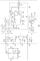
図9は、図6の制御回路の変形例を示す回路図である。図9の制御回路100cは、図6の構成に加えて、増幅回路50、スイッチSW8、およびバッファ60を備える。
図9は、図6の制御回路の変形例を示す回路図である。図9の制御回路100cは、図6の構成に加えて、増幅回路50、スイッチSW8、およびバッファ60を備える。
増幅回路50は、電流検出部30cに設けられる。増幅回路50は、検出抵抗Rsに生ずる電圧降下(検出電圧)Vsと、所定のオフセット電圧VOFSとの差分を利得Aで増幅し、パネル電流Ipを示す電圧値V_Ipとして出力する。
V_Ip=A×(Vs-VOFS) …(1)
V_Ip=A×(Vs-VOFS) …(1)
具体的には増幅回路50は、バッファ52、演算増幅器54、第1抵抗R11~第4抵抗R14、電圧源(D/Aコンバータ)56を含む。電圧源56は、入力されたデジタル値に応じた所定の電圧Vaを生成する。バッファ52は、検出抵抗Rsに生ずる検出電圧Vsを受けるボルテージフォロアである。第1抵抗R11は、バッファ52の出力と演算増幅器54の第1入力端子との間に設けられる。第2抵抗R12は、演算増幅器54の第1入力端子と固定電圧端子(接地端子)の間に設けられる。第3抵抗R13は、その一端に所定の電圧Vaを受け、その他端が演算増幅器54の第2入力端子と接続される。第4抵抗R14は、演算増幅器54の第2入力端子と演算増幅器54の出力端子の間に設けられる。
この増幅回路50においては、利得Aおよびオフセット電圧VOFSはそれぞれ、式(2)、(3)で与えられる。
A=R12・(R13+R14)/(R13・(R11+R12)) …(2)
VOFS=R14・(R11+R12)/(R12・(R13+R14))×Va …(3)
A=R12・(R13+R14)/(R13・(R11+R12)) …(2)
VOFS=R14・(R11+R12)/(R12・(R13+R14))×Va …(3)
ここでR11=R13=R1、R12=R14=R2のとき、式(2a)、(3a)、(4)が成り立つ。
A=R2/R1 …(2a)
VOFS=Va …(3a)
V_Ip=R2/R1×(Vs-Va) …(4)
A=R2/R1 …(2a)
VOFS=Va …(3a)
V_Ip=R2/R1×(Vs-Va) …(4)
電流検出部30cは、A/Dコンバータ24の前段に設けられたバッファ60を備える。バッファ60は、セレクタ22を介してパネル電圧VPを受けるボルテージフォロアである。A/Dコンバータ24は、バッファ60の出力電圧VXをサンプルホールドし、サンプルホールドした値をデジタル値に変換する。A/Dコンバータ24の入力段には、一般的にスイッチと、キャパシタが設けられる。
スイッチSW8は、増幅回路50の入力と出力の間に設けられる。スイッチSW8のオン状態において、増幅回路50はバイパスされる。
以上が制御回路100cの構成である。続いてそのキャリブレーション動作の一例を説明する。まず、タッチパネル4の抵抗値に応じて、言い換えればパネル電流IPに応じて検出抵抗Rsの抵抗値が最適化される。これにより、検出電圧Vsのレンジが最適化される。
また電圧Vaすなわちオフセット電圧VOFSが最適化される。タッチパネル4に接触しない状態においてタッチパネル4に初期電流Iinitが流れるとき、検出抵抗Rsには、式(5)の初期電圧Vinitが発生する。
Vinit=Rs×K1×Iinit …(5)
このときスイッチSW8はオンし、V_Ip=Vinitとなり、A/Dコンバータ34により初期電圧Vinitに対応するデジタル値が測定され、Va=Vinitとなるように電圧源56にデジタル値が与えられる。
Vinit=Rs×K1×Iinit …(5)
このときスイッチSW8はオンし、V_Ip=Vinitとなり、A/Dコンバータ34により初期電圧Vinitに対応するデジタル値が測定され、Va=Vinitとなるように電圧源56にデジタル値が与えられる。
スイッチSW8をオンする代わりに、Va=0に設定してもよい。この場合、A/Dコンバータ34により式(6)の電圧値V_Ipが測定される。
V_Ip=R2/R1×Vinit …(6)
測定された電圧値V_Ipから初期電圧Vinitを算出でき、Va=Vinitとなるように電圧源56にデジタル値を与えてもよい。
V_Ip=R2/R1×Vinit …(6)
測定された電圧値V_Ipから初期電圧Vinitを算出でき、Va=Vinitとなるように電圧源56にデジタル値を与えてもよい。
実動作状態において、タッチパネル4にユーザが接触したときの検出電圧Vsは、
Vs=(Iinit+ΔI)・Rs=Vinit+ΔV …(7)
となり、式(8)を得る。
V_Ip=A×(Vs-Va)=A×(Vinit+ΔV-Vinit)=A×ΔV
…(8)
つまり、V_Ipは、ユーザがタッチパネル4に接触したことによる電流の変化分ΔIに比例した電圧となる。
Vs=(Iinit+ΔI)・Rs=Vinit+ΔV …(7)
となり、式(8)を得る。
V_Ip=A×(Vs-Va)=A×(Vinit+ΔV-Vinit)=A×ΔV
…(8)
つまり、V_Ipは、ユーザがタッチパネル4に接触したことによる電流の変化分ΔIに比例した電圧となる。
ユーザが接触したことによる電流変化量ΔIは、接触抵抗が大きいほど小さくなる。この実施の形態では、電流変化量ΔIに応じた電圧変化量ΔVを、増幅回路50によって増幅することにより、接触抵抗が大きなタッチパネル4であっても、2点間の距離ΔXをより正確に検出することができる。
またタッチパネル4の接触抵抗が大きい状況において、バッファ60が設けられていない場合、A/Dコンバータ24の入力段のキャパシタが、タッチパネル4の抵抗成分を介して充電されることになる。したがって接触抵抗が大きい場合、充電速度が遅くなりサンプルホールドに要する時間が長くなる。サンプルホールド時間が長くなると、座標検出の応答速度が遅くなる。
これに対して図9の制御回路100cでは、出力インピーダンスが小さなバッファ60を設けることにより、充電速度を速めることができる。これによりサンプルホールド時間を短くでき、ひいては座標検出の応答速度を速めることができる。
以上、本発明について、実施の形態をもとに説明した。この実施の形態は例示であり、それらの各構成要素や各処理プロセスの組み合わせにいろいろな変形例が可能なこと、またそうした変形例も本発明の範囲にあることは当業者に理解されるところである。以下、こうした変形例について説明する。
マルチタッチ状態において、座標生成部48はパネル電圧VPxに応じた座標X3を、2点PU1、PU2の中点であると推定して、もとの座標X1、X2を決定したが、本発明はそれに限定されず、さらに複雑なアルゴリズムを用いてもよい。
実施の形態では、第1状態φxと第2状態φyにおいて、図1の制御回路100の一部を共有する構成としたが、完全に別個に設けてもよい。また、X方向、Y方向のみのいずれか一方のみに本発明を適用してもよい。
実施の形態では、4端子のタッチパネル4を制御する場合を説明したが、本発明はそれに限定されず、その他のタッチパネル4にも適用することが可能である。
また、実施の形態ではマルチタッチとして2点を例に説明したが、当業者であればそれを3点以上に拡張でき、それも本発明に含まれる。
実施の形態にもとづき、具体的な用語を用いて本発明を説明したが、実施の形態は、本発明の原理、応用を示しているにすぎず、実施の形態には、請求の範囲に規定された本発明の思想を逸脱しない範囲において、多くの変形例や配置の変更が認められる。
1…電子機器、P1x…第1端子、P1y…第3端子、RF1…第1抵抗膜、Pc1…第1端子、SW1…バイパススイッチ、R1…第1抵抗、SEL1…第1セレクタ、2…入力装置、P2x…第2端子、P2y…第4端子、RF2…第2抵抗膜、Pc2…第2端子、R2…第2抵抗、SEL2…第2セレクタ、4…タッチパネル、6…指、8…LCD、10…電圧生成部、11…レギュレータ、12…演算増幅器、14…出力トランジスタ、20…電圧検出部、22…セレクタ、24…A/Dコンバータ、30…電流検出部、32…I/V変換部、34…A/Dコンバータ、Rs…検出抵抗、38…検出トランジスタ、40…演算部、42…マルチタッチ判定部、44…距離演算部、46…テーブル、48…座標生成部、100…制御回路、50…増幅回路、52…バッファ、54…演算増幅器、R11…第1抵抗、R12…第2抵抗、R13…第3抵抗、R14…第4抵抗、60…バッファ。
本発明は、電子デバイスの入力装置に利用できる。
Claims (13)
- 第1、第2、第3端子と、一辺が前記第1端子と接続され、それと対向する辺が前記第2端子と接続される第1抵抗膜と、前記第1抵抗膜とギャップを隔てて配置され、その一辺が前記第3端子と接続される第2抵抗膜と、を有するタッチパネルの制御回路であって、
前記第1、第2端子それぞれに所定の第1、第2バイアス電圧を印加する電圧生成部と、
前記第3端子に生ずるパネル電圧を検出する電圧検出部と、
前記第1端子、前記第1抵抗膜、前記第2端子を含む経路に流れるパネル電流を検出する電流検出部と、
前記パネル電圧および前記パネル電流の値にもとづき、ユーザが接触した座標を判定する座標判定部と、
を備え、
前記電圧生成部は、
前記第1端子、前記第1抵抗膜、前記第2端子を含む経路の前記第1端子側の延長上に設けられた出力トランジスタを有し、前記第1端子に前記第1バイアス電圧を印加するレギュレータを含み、
前記電流検出部は、
前記出力トランジスタとカレントミラー回路を形成するように接続された検出トランジスタと、
当該検出トランジスタの経路上に設けられた検出抵抗と、
前記検出抵抗の電圧降下と所定の電圧との差分を増幅し、前記パネル電流を示す値として出力する増幅回路と、
を含むことを特徴とする制御回路。 - 第1、第2、第3、第4端子と、その一辺が前記第1端子と接続され、それと対向する辺が前記第2端子と接続される第1抵抗膜と、前記第1抵抗膜とギャップを隔てて配置され、その一辺が前記第3端子と接続され、それと対向する辺が前記第4端子と接続される第2抵抗膜と、を有するタッチパネルの制御回路であって、
第1状態において前記第1、第2端子それぞれに所定の第1、第2バイアス電圧を印加し、前記第3、第4端子をハイインピーダンス状態とし、第2状態において前記第3、第4端子それぞれに所定の第1、第2バイアス電圧を印加し、前記第1、第2端子をハイインピーダンス状態とする電圧生成部と、
前記第1状態において、前記第3、第4端子の一方に生ずるパネル電圧を検出し、前記第2状態において、前記第1、第2端子の一方に生ずるパネル電圧を検出する電圧検出部と、
前記第1状態において、前記第1端子、前記第1抵抗膜、前記第2端子を含む経路に流れるパネル電流を検出し、前記第2状態において、前記第3端子、前記第2抵抗膜、前記第4端子を含む経路に流れるパネル電流を検出する電流検出部と、
前記パネル電圧および前記パネル電流の値にもとづき、ユーザが接触した座標を判定する座標判定部と、
を備え、
前記電圧生成部は、
出力トランジスタを有し、前記第1バイアス電圧を生成するレギュレータと、
その入力端子に前記第1バイアス電圧を受け、その第1出力端子に前記第1端子が接続され、その第2出力端子に前記第3端子が接続され、前記第1状態において前記第1出力端子側にオンし、前記第2状態において前記第2出力端子側にオンするセレクタと、
を含み、
前記電流検出部は、
前記出力トランジスタとカレントミラー回路を形成するように接続された検出トランジスタと、
当該検出トランジスタの経路上に設けられた検出抵抗と、
前記検出抵抗の電圧降下と所定の電圧との差分を増幅し、前記パネル電流を示す値として出力する増幅回路と、
を含むことを特徴とする制御回路。 - 第1、第2、第3、第4端子と、その一辺が前記第1端子と接続され、それと対向する辺が前記第2端子と接続される第1抵抗膜と、前記第1抵抗膜とギャップを隔てて配置され、その一辺が前記第3端子と接続され、それと対向する辺が前記第4端子と接続される第2抵抗膜と、を有するタッチパネルの制御回路であって、
第1状態において前記第1、第2端子それぞれに所定の第1、第2バイアス電圧を印加し、前記第3、第4端子をハイインピーダンス状態とし、第2状態において前記第3、第4端子それぞれに所定の第1、第2バイアス電圧を印加し、前記第1、第2端子をハイインピーダンス状態とする電圧生成部と、
前記第1状態において、前記第3、第4端子それぞれに生ずるパネル電圧を個別に検出し、前記第2状態において、前記第1、第2端子それぞれに生ずるパネル電圧を個別に検出する電圧検出部と、
前記第1状態において、前記第1端子、前記第1抵抗膜、前記第2端子を含む経路に流れるパネル電流を検出し、前記第2状態において、前記第3端子、前記第2抵抗膜、前記第4端子を含む経路に流れるパネル電流を検出する電流検出部と、
前記パネル電圧および前記パネル電流の値にもとづき、ユーザが接触した座標を判定する座標判定部と、
を備え、
前記電圧生成部は、
出力トランジスタを有し、前記第1バイアス電圧を生成するレギュレータと、
その入力端子に前記第1バイアス電圧を受け、その第1出力端子に前記第1端子が接続され、その第2出力端子に前記第3端子が接続され、前記第1状態において前記第1出力端子側にオンし、前記第2状態において前記第2出力端子側にオンするセレクタと、
を含み、
前記電流検出部は、
前記出力トランジスタとカレントミラー回路を形成するように接続された検出トランジスタと、
当該検出トランジスタの経路上に設けられた検出抵抗と、
前記検出抵抗の電圧降下と所定の電圧との差分を増幅し、前記パネル電流を示す値として出力する増幅回路と、
を含むことを特徴とする制御回路。 - 前記増幅回路は、
前記検出抵抗の電圧降下を受けるバッファと、
演算増幅器と、
前記バッファの出力と前記演算増幅器の第1入力端子との間に設けられた第1抵抗と、
前記演算増幅器の前記第1入力端子と固定電圧端子の間に設けられた第2抵抗と、
その一端に前記所定の電圧を受け、その他端が前記演算増幅器の第2入力端子と接続された第3抵抗と、
前記演算増幅器の前記第2入力端子と前記演算増幅器の出力端子の間に設けられた第4抵抗と、
を含むことを特徴とする請求項1から3のいずれかに記載の制御回路。 - 前記電圧検出部は、
前記パネル電圧を受けるバッファと、
前記バッファの出力電圧をサンプルホールドし、サンプルホールドした値をデジタル値に変換するA/Dコンバータと、
を含むことを特徴とする請求項1から4のいずれかに記載の制御回路。 - 前記電流検出部は、前記第1状態と前記第2状態において、前記出力トランジスタと前記検出トランジスタのミラー比を切りかえ可能に構成されることを特徴とする請求項2または3に記載の制御回路。
- 前記電流検出部は、前記第1状態と前記第2状態において、前記検出抵抗の抵抗値を切りかえ可能に構成されることを特徴とする請求項2または3に記載の制御回路。
- 前記座標判定部は、前記パネル電流の値が所定の値より大きいとき、ユーザが複数の点を接触しているものと判定することを特徴とする請求項1から7のいずれかに記載の制御回路。
- ユーザが2点に接触しているとき、前記パネル電流の値にもとづいて前記2点の座標間隔を決定することを特徴とする請求項1から7のいずれかに記載の制御回路。
- ユーザがパネルに接触していないときに測定された前記パネル電流と、接触したときの前記パネル電流の差分にもとづいて、前記2点の座標間隔を決定することを特徴とする請求項9に記載の制御回路。
- 前記座標判定部は、
前記パネル電圧にもとづいて前記2点の中心座標を決定し、当該中心座標に前記2点の座標間隔に応じた値を加算することで、前記2点の一方の座標を決定し、前記中心座標から前記2点の座標間隔に応じた値を減算することで、前記2点の他方の座標を決定することを特徴とする請求項9に記載の制御回路。 - 第1、第2、第3端子と、一辺が前記第1端子と接続され、それと対向する辺が前記第2端子と接続される第1抵抗膜と、前記第1抵抗膜とギャップを隔てて配置され、その一辺が前記第3端子と接続される第2抵抗膜と、を有するタッチパネルと、
前記タッチパネルを制御する請求項1から11のいずれかに記載の制御回路と、
を備えることを特徴とするタッチパネル入力装置。 - 請求項12に記載のタッチパネル入力装置を備えることを特徴とする電子機器。
Priority Applications (1)
| Application Number | Priority Date | Filing Date | Title |
|---|---|---|---|
| US13/961,415 US9207803B2 (en) | 2011-02-08 | 2013-08-07 | Touch panel control circuit |
Applications Claiming Priority (2)
| Application Number | Priority Date | Filing Date | Title |
|---|---|---|---|
| JP2011-025017 | 2011-02-08 | ||
| JP2011025017A JP5797908B2 (ja) | 2011-02-08 | 2011-02-08 | タッチパネルの制御回路およびそれを用いたタッチパネル入力装置、電子機器 |
Related Child Applications (1)
| Application Number | Title | Priority Date | Filing Date |
|---|---|---|---|
| US13/961,415 Continuation US9207803B2 (en) | 2011-02-08 | 2013-08-07 | Touch panel control circuit |
Publications (1)
| Publication Number | Publication Date |
|---|---|
| WO2012108182A1 true WO2012108182A1 (ja) | 2012-08-16 |
Family
ID=46638403
Family Applications (1)
| Application Number | Title | Priority Date | Filing Date |
|---|---|---|---|
| PCT/JP2012/000804 Ceased WO2012108182A1 (ja) | 2011-02-08 | 2012-02-07 | タッチパネルの制御回路およびそれを用いたタッチパネル入力装置、電子機器 |
Country Status (4)
| Country | Link |
|---|---|
| US (1) | US9207803B2 (ja) |
| JP (1) | JP5797908B2 (ja) |
| TW (1) | TWI543061B (ja) |
| WO (1) | WO2012108182A1 (ja) |
Families Citing this family (7)
| Publication number | Priority date | Publication date | Assignee | Title |
|---|---|---|---|---|
| CN102981688B (zh) * | 2012-11-19 | 2016-06-15 | 深圳市新国都技术股份有限公司 | 一种五线电阻屏控制电路 |
| TWI488023B (zh) * | 2013-04-29 | 2015-06-11 | Ili Technology Corp | 電流電壓轉換器及其電子裝置 |
| JP6158615B2 (ja) * | 2013-07-05 | 2017-07-05 | 富士通コンポーネント株式会社 | タッチパネル |
| TWI499963B (zh) * | 2013-09-13 | 2015-09-11 | Weltrend Semiconductor Inc | 在薄膜輸入裝置上偵測觸壓點的方法 |
| JP6649163B2 (ja) * | 2016-04-08 | 2020-02-19 | ローム株式会社 | タッチパネルの制御回路、ならびにそれを用いたタッチパネル入力装置、電子機器 |
| KR20180080739A (ko) * | 2017-01-04 | 2018-07-13 | 삼성디스플레이 주식회사 | 터치 센서 및 이를 포함하는 터치 센싱 시스템 |
| JP6908493B2 (ja) * | 2017-10-11 | 2021-07-28 | ローム株式会社 | タッチパネルの制御回路、制御方法、それを用いたタッチ式入力装置、電子機器 |
Citations (4)
| Publication number | Priority date | Publication date | Assignee | Title |
|---|---|---|---|---|
| JPH07160402A (ja) * | 1993-12-13 | 1995-06-23 | Nippondenso Co Ltd | アナログ・タッチスイッチ |
| JP2007156875A (ja) * | 2005-12-06 | 2007-06-21 | Sony Corp | タッチパネルおよび多重押し検出方法 |
| JP2010092347A (ja) * | 2008-10-09 | 2010-04-22 | Yamaha Corp | タッチパネル装置 |
| JP2011076591A (ja) * | 2009-07-07 | 2011-04-14 | Rohm Co Ltd | タッチパネルの制御回路、制御方法およびそれらを用いたタッチパネル入力装置、電子機器 |
Family Cites Families (10)
| Publication number | Priority date | Publication date | Assignee | Title |
|---|---|---|---|---|
| JPS6484325A (en) * | 1987-09-28 | 1989-03-29 | Oki Electric Ind Co Ltd | Multiplex input detecting system in pressure sensitive type input device |
| JP3402858B2 (ja) * | 1995-07-20 | 2003-05-06 | キヤノン株式会社 | 座標検出方法及び装置及びコンピュータ制御装置 |
| JPH09134253A (ja) * | 1995-11-13 | 1997-05-20 | Ricoh Co Ltd | タッチパネル装置 |
| JP3221368B2 (ja) * | 1997-09-17 | 2001-10-22 | 日本電気株式会社 | 抵抗膜方式タブレット及びその制御方法並びにその方法を実現するためのプログラムを記録した記録媒体 |
| EP1422601A4 (en) * | 2001-08-22 | 2006-10-18 | Sharp Kk | TOUCH SENSOR, TOUCH SENSOR DISPLAY, AND POSITION DATA GENERATION METHOD |
| KR100847813B1 (ko) * | 2001-12-27 | 2008-07-23 | 엘지디스플레이 주식회사 | 터치패널 구동장치 및 방법 |
| JP4295280B2 (ja) * | 2003-08-29 | 2009-07-15 | ノキア コーポレイション | タッチベースユーザ入力装置で2点ユーザ入力を認識する方法および装置 |
| KR20060132941A (ko) * | 2004-03-23 | 2006-12-22 | 로무 가부시키가이샤 | 반도체 집적 회로 장치 및 그것을 이용한 스위칭 전원 장치 |
| JP2009048233A (ja) | 2007-08-13 | 2009-03-05 | Mitsubishi Electric Corp | タッチパネル入力装置 |
| KR101077854B1 (ko) * | 2008-05-22 | 2011-10-31 | (주)멜파스 | 복수의 접촉 입력을 감지하는 방법 및 장치 |
-
2011
- 2011-02-08 JP JP2011025017A patent/JP5797908B2/ja active Active
-
2012
- 2012-02-07 WO PCT/JP2012/000804 patent/WO2012108182A1/ja not_active Ceased
- 2012-02-08 TW TW101104087A patent/TWI543061B/zh not_active IP Right Cessation
-
2013
- 2013-08-07 US US13/961,415 patent/US9207803B2/en active Active
Patent Citations (4)
| Publication number | Priority date | Publication date | Assignee | Title |
|---|---|---|---|---|
| JPH07160402A (ja) * | 1993-12-13 | 1995-06-23 | Nippondenso Co Ltd | アナログ・タッチスイッチ |
| JP2007156875A (ja) * | 2005-12-06 | 2007-06-21 | Sony Corp | タッチパネルおよび多重押し検出方法 |
| JP2010092347A (ja) * | 2008-10-09 | 2010-04-22 | Yamaha Corp | タッチパネル装置 |
| JP2011076591A (ja) * | 2009-07-07 | 2011-04-14 | Rohm Co Ltd | タッチパネルの制御回路、制御方法およびそれらを用いたタッチパネル入力装置、電子機器 |
Also Published As
| Publication number | Publication date |
|---|---|
| JP2012164197A (ja) | 2012-08-30 |
| US9207803B2 (en) | 2015-12-08 |
| JP5797908B2 (ja) | 2015-10-21 |
| TW201243692A (en) | 2012-11-01 |
| TWI543061B (zh) | 2016-07-21 |
| US20140168113A1 (en) | 2014-06-19 |
Similar Documents
| Publication | Publication Date | Title |
|---|---|---|
| JP5086394B2 (ja) | タッチパネルの制御回路、制御方法およびそれらを用いたタッチパネル入力装置、電子機器 | |
| JP5797908B2 (ja) | タッチパネルの制御回路およびそれを用いたタッチパネル入力装置、電子機器 | |
| JP5450211B2 (ja) | タッチパネルの制御回路、制御方法およびそれらを用いたタッチパネル入力装置、電子機器 | |
| KR102496317B1 (ko) | 센싱 회로 및 이를 포함하는 터치 센서 | |
| US10156949B2 (en) | Force-touch sensor with multilayered electrodes | |
| JP6908493B2 (ja) | タッチパネルの制御回路、制御方法、それを用いたタッチ式入力装置、電子機器 | |
| WO2019011013A1 (zh) | 触控电路、触控面板、显示面板和显示装置 | |
| Kim et al. | A touchpad for force and location sensing | |
| US10289248B2 (en) | Control circuit and control method of touch panel, and touch panel input device and electronic device using the same | |
| US20190277800A1 (en) | Conductance measurement circuit | |
| JP4622631B2 (ja) | 接触位置座標検出方法および装置 | |
| WO2019142804A1 (ja) | 抵抗膜タッチパネルの制御回路、タッチ式入力装置 | |
| US9423919B2 (en) | Touch panel | |
| US12554361B2 (en) | Touch-sensitive apparatus and method | |
| JP2019144878A (ja) | タッチパネルの制御回路、制御方法、それを用いたタッチ式入力装置、電子機器 | |
| JP2019139293A (ja) | タッチパネルのコントローラ、ならびにそれを用いたタッチ式入力装置、電子機器 | |
| JP2014013441A (ja) | タッチパネルの制御回路、制御方法およびそれらを用いたタッチパネル入力装置、電子機器 | |
| JP2002049465A (ja) | タブレット装置 |
Legal Events
| Date | Code | Title | Description |
|---|---|---|---|
| 121 | Ep: the epo has been informed by wipo that ep was designated in this application |
Ref document number: 12744412 Country of ref document: EP Kind code of ref document: A1 |
|
| NENP | Non-entry into the national phase |
Ref country code: DE |
|
| 122 | Ep: pct application non-entry in european phase |
Ref document number: 12744412 Country of ref document: EP Kind code of ref document: A1 |