WO2012105327A1 - 基板搬送用キャリアの製造方法、基板搬送用キャリア - Google Patents
基板搬送用キャリアの製造方法、基板搬送用キャリア Download PDFInfo
- Publication number
- WO2012105327A1 WO2012105327A1 PCT/JP2012/051090 JP2012051090W WO2012105327A1 WO 2012105327 A1 WO2012105327 A1 WO 2012105327A1 JP 2012051090 W JP2012051090 W JP 2012051090W WO 2012105327 A1 WO2012105327 A1 WO 2012105327A1
- Authority
- WO
- WIPO (PCT)
- Prior art keywords
- adhesive layer
- substrate
- support
- carrier
- silicate compound
- Prior art date
- Legal status (The legal status is an assumption and is not a legal conclusion. Google has not performed a legal analysis and makes no representation as to the accuracy of the status listed.)
- Ceased
Links
Images
Classifications
-
- H—ELECTRICITY
- H05—ELECTRIC TECHNIQUES NOT OTHERWISE PROVIDED FOR
- H05K—PRINTED CIRCUITS; CASINGS OR CONSTRUCTIONAL DETAILS OF ELECTRIC APPARATUS; MANUFACTURE OF ASSEMBLAGES OF ELECTRICAL COMPONENTS
- H05K3/00—Apparatus or processes for manufacturing printed circuits
-
- H—ELECTRICITY
- H05—ELECTRIC TECHNIQUES NOT OTHERWISE PROVIDED FOR
- H05K—PRINTED CIRCUITS; CASINGS OR CONSTRUCTIONAL DETAILS OF ELECTRIC APPARATUS; MANUFACTURE OF ASSEMBLAGES OF ELECTRICAL COMPONENTS
- H05K2203/00—Indexing scheme relating to apparatus or processes for manufacturing printed circuits covered by H05K3/00
- H05K2203/01—Tools for processing; Objects used during processing
- H05K2203/0147—Carriers and holders
- H05K2203/016—Temporary inorganic, non-metallic carrier, e.g. for processing or transferring
Definitions
- the present invention relates to a carrier for transporting a substrate for transporting a substrate such as a printed wiring board on which a semiconductor device and a small component are mounted, and a method for manufacturing the same.
- FPC flexible printed wiring board
- Patent Document 1 a substrate carrier is manufactured by bringing a resin sheet obtained from a mixture of a silicate compound and polydimethylsiloxane having a predetermined structure into close contact with a base.
- the FPC comes into contact with various chemicals such as an alkaline plating solution during the manufacturing process. Therefore, the carrier for transportation is exposed to various chemicals in the same manner. In particular, the transport carrier is usually used repeatedly, and thus is exposed to the medicine a plurality of times.
- the present inventors examined the carrier for board
- an object of the present invention is to provide a carrier for transporting a substrate and a method for manufacturing the same, in which the occurrence of peeling of an adhesive layer is small even after contact with a chemical, particularly an alkaline solution.
- the inventors of the present invention have made extensive studies on the problems of the prior art and found that the adhesion between the adhesive layer and the base (support) is not always sufficient in the conventional substrate transport carrier. Based on this finding, the present inventors have found that the problem can be solved by the following configuration.
- a method for producing a carrier for transporting a substrate comprising a support having an adhesive layer fixed thereon, A surface modification step of bringing the silicate compound into contact with the support and chemically modifying the surface of the support;
- a method for producing a carrier for transporting a substrate comprising: an adhesive layer forming step of forming an adhesive layer on a surface-modified support.
- substrate conveyance by which the support body surface by which the adhesion layer is fixed is chemically modified with the silicate compound.
- the present invention it is possible to provide a carrier for transporting a substrate and a method for manufacturing the same, which hardly cause peeling of the adhesive layer even after coming into contact with a chemical, particularly an alkaline solution.
- substrate conveyance of this invention and its manufacturing method are explained in full detail.
- a characteristic point of the present invention compared with the prior art, there is a point of performing a step of bringing a silicate compound and a support into contact before producing the adhesive layer.
- the surface of the support is modified with a silicate compound, and the silicate compound contributes to improving the adhesion between the support and the adhesive layer.
- a support body is a glass support body, it is excellent in affinity and reactivity with a silicate compound, an adhesion layer adheres more on a support body, and peeling of an adhesion layer is suppressed.
- an adhesion layer contains a silicone resin
- it has affinity with the silicate compound chemically bonded on the support body surface, and the adhesiveness between an adhesion layer and a support body improves more.
- an adhesive layer is produced using a silicate-modified silicone resin, a strong covalent bond is formed between the adhesive layer and the support, and the adhesion of the adhesive layer to the support is further improved.
- an alkali washing process is an arbitrary process implemented as needed.
- Alkali washing step Step of washing the support with an alkaline aqueous solution
- surface modification step Step of bringing the silicate compound and the support into contact with each other and chemically modifying the surface of the support (adhesion layer forming step)
- adheresion layer forming step On the surface-modified support Step of forming an adhesive layer in the following Each step will be described in detail.
- the alkali cleaning step is a step of cleaning the support using an alkaline aqueous solution. By carrying out this step, it is possible to remove impurities adhering to the support surface and to improve the reactivity between the support surface and a silicate compound described later. As a result, the adhesion between the adhesive layer and the support described later is further improved.
- the materials used will be described in detail below, and the procedure of the subsequent steps will be described in detail. In addition, when the support body to be used has a desired surface property already, this process does not need to be implemented.
- the aqueous solution used in this step exhibits alkalinity. Of these, pH of 8 or more is preferable and pH of 9 to 12 is more preferable in terms of removing impurities and improving the reactivity of the support surface.
- As the solvent in the aqueous solution water is usually used. In addition, you may use an organic solvent (for example, alcohol solvent etc.) as needed.
- an alkali compound is usually added.
- the alkali compound used is not particularly limited, and examples thereof include sodium hydroxide, potassium hydroxide, sodium carbonate, alkylammonium salt, and alkylarylammonium salt.
- the amount of the compound added is appropriately adjusted so that the solution falls within the above pH range.
- the type of the support is not particularly limited as long as it can support an adhesive layer described later, and may be, for example, a silicon wafer, a glass substrate, a resin substrate, or a metal substrate.
- a glass substrate is preferable because it has excellent reactivity with a silicate compound described later, better adhesion to the adhesive layer, and excellent chemical resistance and heat resistance.
- the glass substrate is not particularly limited, and examples thereof include soda lime glass, soda lime aluminum glass, and borosilicate glass.
- the length and width of the support used are adjusted as appropriate according to the size of the conveyed object.
- the thickness of the support is not particularly limited, but is often about 0.3 to 5.0 mm from the viewpoint of suppressing cracking during transportation.
- the method for washing the support with an alkaline aqueous solution is not particularly limited, and examples thereof include a coating method in which an alkaline aqueous solution is applied onto the surface of the support, and an immersion method in which the support is immersed in the alkaline aqueous solution.
- the contact time between the support and the alkaline aqueous solution is appropriately set according to the type of the support used, but is preferably about 0.5 to 10 minutes from the viewpoint of impurity removal and productivity. .
- the support surface may be further washed with water and dried as necessary.
- the surface modification step is performed after the alkali cleaning step, and is a step in which the silicate compound and the support are brought into contact with each other.
- the support surface is chemically modified with the silicate compound. More specifically, by performing this step, the silicate compound is chemically bonded to the support surface, and a layer of the silicate compound is formed on the support surface.
- the adhesion between the adhesive layer formed thereon and the support is further improved.
- the silicate compound of the present invention is a metal alkoxide (alkoxysilane compound (particularly, tetraalkoxysilane compound)) made of silicon (Si) or an oligomer thereof.
- An oligomer is a compound having a siloxane (—Si—O—Si—) skeleton in the main chain and an alkoxy group (RO) introduced in the side chain.
- (R) which is the alkyl part of the alkoxy group (RO) is exemplified by a methyl group, an ethyl group, a propyl group, and the like.
- This silicate compound has the property of reacting with water.
- the silicate compound is desirably a tetramer to a 16-mer (a tetramer or more and a 16-mer or less).
- the effect of the characteristics of the silicate compound is small if it is less than the tetramer, and the viscosity of the silicate compound is high if it is larger than the 16-mer, so that it is difficult to handle at the time of production.
- examples of the silicate compound used in the present invention include methyl silicate, ethyl silicate (TEOS), propyl silicate, and the like, or oligomers thereof. From the viewpoint of quality stability and safety, ethyl silicate (TEOS) or an oligomer thereof is preferred.
- the adhesiveness to the support body of an adhesion layer improves more.
- the pressure-sensitive adhesive layer is a silicone resin layer (more preferably, the pressure-sensitive adhesive layer is a resin layer formed by reacting terminal silicate-modified silicone), the effect of the present invention is more excellent.
- a preferred embodiment of the silicate compound represented by the chemical formula 1 includes a compound represented by the following formula (X).
- R 1 is an alkyl group having 4 or less carbon atoms
- n is an integer of 4 to 16.
- the silicate compound may be synthesized according to a known method, or a commercially available product (for example, manufactured by Tama Chemical Industries) may be used.
- the method for bringing the silicate compound into contact with the support surface is not particularly limited, and examples thereof include a coating method for applying the silicate compound on the support surface, and an immersion method for immersing the support in the silicate compound.
- Specific examples of the coating method include a bar coating method, a spin coating method, a knife coating method, a doctor blade method, and the like.
- the viscosity may be adjusted by adding various solvents (for example, water, alcohol solvent, ketone solvent, etc.) to the silicate compound as necessary.
- the contact time (treatment time) between the support and the silicate compound is appropriately set depending on the type of the silicate compound used, but from the viewpoint of productivity, reactivity of the silicate compound, etc., 0.5 Minutes or more, and preferably about 1 to 10 minutes. Moreover, you may perform an air drying process or heat processing after a contact with a silicate compound and a support body as needed.
- the pressure-sensitive adhesive layer forming step is performed after the surface modification step, and is a step of forming the pressure-sensitive adhesive layer on the chemically modified surface of the support. By carrying out this step, an adhesive layer on which a substrate such as FPC is disposed is formed on the surface. First, the adhesive layer will be described in detail, and the procedure of the subsequent process will be described in detail.
- the pressure-sensitive adhesive layer is a layer (resin layer) that can be peelably adhered to a substrate disposed on the surface thereof.
- the adhesive layer can hold the position of the substrate in close contact with the surface thereof, and can prevent the substrate from warping or twisting.
- the adhesive force between the adhesive layer and the support is higher than the adhesive force between the adhesive layer and the substrate (for example, FPC) disposed on the surface thereof. As a result, the substrate can be easily peeled from the pressure-sensitive adhesive layer without causing the pressure-sensitive adhesive layer to peel off.
- the pressure-sensitive adhesive layer to be formed is not particularly limited as long as its surface can be peeled and adhered to the lower surface of the substrate.
- the resin contained in the pressure-sensitive adhesive layer include urethane resin, polyvinyl alcohol resin, and silicone. Resin. Among these, a silicone resin is preferable from the viewpoint of chemical resistance and peelability. That is, the adhesive layer is preferably a silicone resin layer.
- a silicone resin layer intends the layer in which a silicone resin is contained as a main component.
- the thickness of the pressure-sensitive adhesive layer is appropriately set according to the type of substrate disposed thereon, but is preferably 0.01 to 10 mm, more preferably 0.03 to 5 mm from the viewpoint of chemical resistance and peelability. .
- the procedure for forming the adhesive layer is not particularly limited, and a method of fixing the film-like adhesive layer on the support, or a liquid composition containing the component constituting the adhesive layer or its precursor is applied on the support. And a method of forming an adhesive layer.
- a method of applying the above composition on a support is preferred in that the adhesion between the support surface-treated with the silicate compound and the adhesive layer is more excellent.
- heat processing is performed as needed for the removal of a solvent, hardening of a precursor, etc.
- the conditions for the heat treatment are appropriately set according to the materials used, but from the viewpoint of stabilizing the adhesive layer, it is preferable to carry out the treatment at 50 to 300 ° C. for 0.5 to 12 hours.
- a silicone resin layer obtained by using a composition obtained by subjecting a mixture having a silicate compound and an organopolysiloxane having a silicate-modified terminal to a hydrolysis reaction and a condensation reaction is used.
- the process of forming on a support body is mentioned. If it is this silicone resin layer, adhesiveness with the support body chemically modified with the silicate compound mentioned above is more excellent.
- the organopolysiloxane it is preferable to use polydimethylsiloxane because the effects of the present invention are more excellent.
- organopolysiloxane is polydimethylsiloxane
- Polydimethylsiloxane is abbreviated as “PDMS”
- polydimethylsiloxane whose terminal is silicate-modified is abbreviated as “modified PDMS”.
- Modified PDMS is a product obtained by modifying the end of PDMS with a silicate compound, for example, PDMS having silanol groups at both ends, and alkoxy which is a hydrolyzable functional group on one or both sides of the main chain of PDMS. What is obtained by reacting the alkoxysilane partial condensate having a group.
- This modified PDMS has a much higher functional group concentration than ordinary PDMS. Further, since the modified PDMS has high condensation reactivity with the silicate compound, the alkoxysilane partial condensate contained in the modified PDMS can be smoothly polymerized by being subjected to a condensation reaction smoothly.
- the modified PDMS used in the present invention preferably has a mass average molecular weight in the range of 5000 or more and 100,000 or less.
- Modified PDMS may be synthesized with reference to a known synthesis method (for example, Japanese Patent No. 4255088) or a commercially available product may be used.
- denatured PDMS (B) is the range of 0.1-10, in the molar ratio of A / B.
- the optimum blending ratio is around 1 in terms of A / B molar ratio.
- the silicate compound is preferably increased.
- composition is produced by hydrolyzing and condensing a mixture having the silicate compound and the modified PDMS.
- silicate compound Since the silicate compound is easily hydrolyzed in the presence of water, the alkoxy group in the molecule of the silicate compound becomes a highly reactive silanol group (—OH group).
- the modified PDMS is also hydrolyzed to form a silanol group (also referred to as “silanol modification”) due to the presence of water.
- the composition is liquid (also referred to as “sol”)
- the composition is applied onto the support as described above, and subjected to heat treatment as necessary to form a desired adhesive layer on the support. Can be formed on top.
- the application method and heating conditions are as described above.
- the composition is applied to a tray such as a mold, and is cured by a drying and firing treatment to be formed into a sheet (plate), and the adhesive layer formed into the sheet is used as a support. It is fixed (held) by adhering or adhering to the surface.
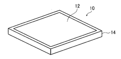
- the substrate transport carrier 10 obtained by the above manufacturing method includes an adhesive layer 12 that is detachably adhered to the lower surface of the substrate that is the object to be transported, and a support 14 on which the adhesive layer is fixed.
- the substrate transport carrier 10 is a carrier capable of transporting a substrate to a process in which a chemical treatment is performed by bonding a sheet-like thin substrate such as a flexible substrate to the surface of the adhesive layer 12.
- the substrate is not limited to a printed wiring board such as an FPC, and is not particularly limited as long as it is a sheet.
- the pressure-sensitive adhesive layer used in this example is formed using a composition obtained by subjecting a mixture having a silicate compound and a polydimethylsiloxane having a silicate-modified end to a hydrolysis reaction and a condensation reaction.
- a composition obtained by subjecting a mixture having a silicate compound and a polydimethylsiloxane having a silicate-modified end to a hydrolysis reaction and a condensation reaction.
- the production of this composition will be specifically described below.
- silicates having the same type and the same characteristics were used as silicates used in ethyl silicate and polydimethylsiloxane obtained by alkoxy-modifying ethyl silicate at both ends.
- a glass substrate manufactured by Matsunami Glass Co., Ltd., length: 100 mm, width: 100 mm, thickness: 0.7 mm
- Semico Clean 56 manufactured by Furuuchi Chemical Co., Ltd .: pH 12
- the glass substrate was taken out and washed with running water for 5 minutes, and then dried in an oven at 120 ° C. for 2 minutes.
- the silicate compound was applied on the surface of the glass substrate according to the following procedures (A) to (C).
- (C) Silicate 40 (manufactured by Tama Chemical Industry Co., Ltd., Si n O (n-1) (RO) 2 (n + 1) : n 4 to 6) was applied by spin coating (1500 rpm).
- Adhesive layer forming process The composition produced above was applied onto a glass substrate chemically modified with a silicate compound by a blade coating method so that the film thickness after baking and drying was 100 ⁇ m. Then, drying baking was performed at 200 degreeC for 1 hour in oven, and the adhesion layer was formed on the glass substrate.
- Example 1 The carrier (A) described in the above (surface modification step) and the above (adhesive layer forming step) were carried out in this order to produce a substrate carrying carrier.
- the said (A) process was implemented without alkali-cleaning a glass substrate.
- Example 2 The (B) process described in the above (surface modification step) and the above (adhesive layer forming step) were carried out in this order to produce a substrate carrying carrier. In addition, in this Example, the said (B) process was implemented without alkali-cleaning a glass substrate.
- Example 3 The (A) treatment described in the above (alkali cleaning step), the above (surface modification step), and the above (adhesive layer forming step) were carried out in this order to produce a substrate transport carrier.
- Example 4 The (C) treatment described in the above (alkali cleaning step), the above (surface modification step), and the above (adhesive layer forming step) were carried out in this order to produce a substrate transport carrier.
- a 50 mm ⁇ 30 mm polyimide film (Kapton 500H: manufactured by Toray DuPont Co., Ltd., thickness 125 ⁇ m) was attached as an adherend on the adhesive layer of the carrier for transporting a substrate manufactured in Examples 1 to 4 and Comparative Example 1. It was immersed in an alkali developer (10% CD-1: manufactured by Fuji Film Electronics Materials Co., Ltd.) at 25 ° C. for 2 minutes. The carrier with the polyimide film was taken out of the developer and dried, and then the polyimide film was peeled from the carrier. After repeating this process from immersion in the alkali developer to peeling of the polyimide film 100 times, peeling of the adhesive layer from the glass substrate was visually confirmed and evaluated according to the following criteria.
- Table 1 below shows experimental conditions and evaluation results of Examples 1 to 4 and Comparative Example 1.
- “-” in the alkali cleaning step column and the surface modification step column means not carried out.
Landscapes
- Engineering & Computer Science (AREA)
- Manufacturing & Machinery (AREA)
- Microelectronics & Electronic Packaging (AREA)
- Supply And Installment Of Electrical Components (AREA)
- Wire Bonding (AREA)
- Laminated Bodies (AREA)
- Adhesives Or Adhesive Processes (AREA)
Abstract
本発明は、薬品、特にアルカリ溶液と接触した後でも粘着層の剥離発生が少ない基板搬送用キャリアの製造方法を提供することを目的とする。本発明の基板搬送用キャリアの製造方法は、基板の搬送に用いられ、基板の下面と剥離可能に密着する粘着層と、粘着層を固定した支持体とを備えた基板搬送用キャリアの製造方法であって、シリケート化合物と支持体表面と接触させ、支持体表面を化学修飾する表面修飾工程と、表面修飾された支持体上に粘着層を形成する粘着層形成工程と、を備える。
Description
本発明は、半導体装置および小型部品が実装されるプリント配線基板等の基板を搬送する基板搬送用キャリアおよびその製造方法に関する。
従来より、電子部品が実装されるプリント配線基板は、あらゆる電子機器に使用されている。一般に、このプリント配線基板は、表面に導体パターンを備えており、近年、電子機器の小型化、軽量化に対応すべく、さまざまなプリント配線基板が提供されている。
このプリント配線基板の中には、フィルム状の絶縁基板表面に導体パターンを備え、基板自体の曲げを可能にしたフレキシブルプリント配線基板(以下、「FPC」と略す。)が存在する。
このFPCは、薄いフィルム状の基板であるため、単体では、ねじれや反りが生じ易い。そこで、このFPCに電子部品実装や、薬品洗浄、プラズマ処理等をする場合、基板の搬送用キャリアという治具を用いる(特許文献1)。
特許文献1では、シリケート化合物と、所定の構造を有するポリジメチルシロキサンとを有する混合物から得られる樹脂シートを、ベース上に密着させて、基板の搬送キャリアを製造している。
特許文献1では、シリケート化合物と、所定の構造を有するポリジメチルシロキサンとを有する混合物から得られる樹脂シートを、ベース上に密着させて、基板の搬送キャリアを製造している。
FPCは、その製造プロセス中において、アルカリ性のめっき液など様々な薬品と接触する。そのため、搬送用キャリアも同じように種々の薬品に曝される。特に、搬送キャリアは、通常繰り返して使用されるため、複数回薬品に曝される。
本発明者らが、特許文献1に記載の基板搬送用キャリアに関して検討を行ったところ、搬送工程中にアルカリ溶液などの薬品と接触する工程がある場合、該工程後に該基板搬送用キャリア上に配置されたFPCなどの被搬送物をキャリアから剥がす際に、樹脂シートの一部が剥がれて、被搬送物に付着してしまうという問題が生じることを見出した。このような樹脂の剥がれなどが生じると、FPCの歩留りの低下を招くことになる。
本発明者らが、特許文献1に記載の基板搬送用キャリアに関して検討を行ったところ、搬送工程中にアルカリ溶液などの薬品と接触する工程がある場合、該工程後に該基板搬送用キャリア上に配置されたFPCなどの被搬送物をキャリアから剥がす際に、樹脂シートの一部が剥がれて、被搬送物に付着してしまうという問題が生じることを見出した。このような樹脂の剥がれなどが生じると、FPCの歩留りの低下を招くことになる。
そこで、本発明は、上記実情に鑑みて、薬品、特にアルカリ溶液と接触した後でも粘着層の剥離発生が少ない基板搬送用キャリアおよびその製造方法を提供することを目的とする。
本発明者らは、従来技術の問題点について鋭意検討を行ったところ、従来の基板搬送用キャリアにおいては、粘着層とベース(支持体)との密着性が必ずしも十分でないことを見出した。本発明者らは、該知見に基づいて、以下の構成により課題が解決できることを見出した。
(1) 基板の搬送に用いられ、基板の下面と剥離可能に密着する粘着層と、
粘着層を固定した支持体とを備えた基板搬送用キャリアの製造方法であって、
シリケート化合物と支持体とを接触させ、支持体表面を化学修飾する表面修飾工程と、
表面修飾された支持体上に粘着層を形成する粘着層形成工程と、を備える基板搬送用キャリアの製造方法。
(2) シリケート化合物が、SinO(n-1)(RO)2(n+1)(R=アルキル基、n=4~16)で表されるシリケート化合物である(1)に記載の基板搬送用キャリアの製造方法。
粘着層を固定した支持体とを備えた基板搬送用キャリアの製造方法であって、
シリケート化合物と支持体とを接触させ、支持体表面を化学修飾する表面修飾工程と、
表面修飾された支持体上に粘着層を形成する粘着層形成工程と、を備える基板搬送用キャリアの製造方法。
(2) シリケート化合物が、SinO(n-1)(RO)2(n+1)(R=アルキル基、n=4~16)で表されるシリケート化合物である(1)に記載の基板搬送用キャリアの製造方法。
(3) 表面修飾工程の前に、アルカリ性水溶液により支持体を洗浄するアルカリ洗浄工程をさらに備える、(1)または(2)に記載の基板搬送用キャリアの製造方法。
(4) 支持体が、ガラス支持体である、(1)~(3)のいずれかに記載の基板搬送用キャリアの製造方法。
(5) 粘着層が、シリコーン樹脂を含む、(1)~(4)のいずれかに記載の基板搬送用キャリアの製造方法。
(6) 基板の搬送に用いられ、基板の下面と剥離可能に密着する粘着層と、
粘着層を固定した支持体とを備えた基板搬送用キャリアであって、
粘着層が固定される側の支持体表面がシリケート化合物で化学修飾されている基板搬送用キャリア。
(7) シリケート化合物が、SinO(n-1)(RO)2(n+1)(R=アルキル基、n=4~16)で表されるシリケート化合物である(6)に記載の基板搬送用キャリア。
(4) 支持体が、ガラス支持体である、(1)~(3)のいずれかに記載の基板搬送用キャリアの製造方法。
(5) 粘着層が、シリコーン樹脂を含む、(1)~(4)のいずれかに記載の基板搬送用キャリアの製造方法。
(6) 基板の搬送に用いられ、基板の下面と剥離可能に密着する粘着層と、
粘着層を固定した支持体とを備えた基板搬送用キャリアであって、
粘着層が固定される側の支持体表面がシリケート化合物で化学修飾されている基板搬送用キャリア。
(7) シリケート化合物が、SinO(n-1)(RO)2(n+1)(R=アルキル基、n=4~16)で表されるシリケート化合物である(6)に記載の基板搬送用キャリア。
本発明によれば、薬品、特にアルカリ溶液と接触した後でも粘着層の剥離発生が少ない基板搬送用キャリアおよびその製造方法を提供することができる。
以下に、本発明の基板搬送用キャリアおよびその製造方法について詳述する。
まず、従来技術と比較した本発明の特徴点としては、粘着層を製造する前に、シリケート化合物と支持体とを接触させる工程を実施する点が挙げられる。該工程を実施することにより、支持体表面上がシリケート化合物で修飾され、該シリケート化合物が支持体と粘着層との間の密着性向上に寄与する。なかでも、支持体がガラス支持体である場合、シリケート化合物との親和性および反応性に優れ、粘着層が支持体上により密着し、粘着層のはく離が抑制される。また、粘着層がシリコーン樹脂を含む場合、支持体表面上に化学結合しているシリケート化合物と親和性があり、粘着層と支持体との間の密着性がより向上する。さらに、シリケート変性シリコーン樹脂を用いて粘着層を製造した場合、粘着層と支持体との間に強固な共有結合が形成され、粘着層の支持体への密着性がより向上する。
まず、従来技術と比較した本発明の特徴点としては、粘着層を製造する前に、シリケート化合物と支持体とを接触させる工程を実施する点が挙げられる。該工程を実施することにより、支持体表面上がシリケート化合物で修飾され、該シリケート化合物が支持体と粘着層との間の密着性向上に寄与する。なかでも、支持体がガラス支持体である場合、シリケート化合物との親和性および反応性に優れ、粘着層が支持体上により密着し、粘着層のはく離が抑制される。また、粘着層がシリコーン樹脂を含む場合、支持体表面上に化学結合しているシリケート化合物と親和性があり、粘着層と支持体との間の密着性がより向上する。さらに、シリケート変性シリコーン樹脂を用いて粘着層を製造した場合、粘着層と支持体との間に強固な共有結合が形成され、粘着層の支持体への密着性がより向上する。
本発明の製造方法の好適態様としては、以下の3つの工程を順番に実施する製造方法が挙げられる。なお、アルカリ洗浄工程は、必要に応じて実施される任意工程である。
(アルカリ洗浄工程) アルカリ性水溶液により支持体を洗浄する工程
(表面修飾工程) シリケート化合物と支持体とを接触させ、支持体表面を化学修飾する工程
(粘着層形成工程) 表面修飾された支持体上に粘着層を形成する工程
以下に、各工程について詳述する。
(アルカリ洗浄工程) アルカリ性水溶液により支持体を洗浄する工程
(表面修飾工程) シリケート化合物と支持体とを接触させ、支持体表面を化学修飾する工程
(粘着層形成工程) 表面修飾された支持体上に粘着層を形成する工程
以下に、各工程について詳述する。
<アルカリ洗浄工程>
アルカリ洗浄工程は、アルカリ性水溶液を用いて支持体を洗浄する工程である。該工程を実施することにより、支持体表面上に付着する不純物の除去や、支持体表面と後述するシリケート化合物との反応性を向上させることができる。結果として、後述する粘着層と支持体との密着性がより向上する。
まず、以下に、使用される材料について詳述し、その後工程の手順について詳述する。なお、使用される支持体がすでに所望の面性状を有している場合は、該工程は実施しなくてもよい。
アルカリ洗浄工程は、アルカリ性水溶液を用いて支持体を洗浄する工程である。該工程を実施することにより、支持体表面上に付着する不純物の除去や、支持体表面と後述するシリケート化合物との反応性を向上させることができる。結果として、後述する粘着層と支持体との密着性がより向上する。
まず、以下に、使用される材料について詳述し、その後工程の手順について詳述する。なお、使用される支持体がすでに所望の面性状を有している場合は、該工程は実施しなくてもよい。
(アルカリ性水溶液)
本工程で使用される水溶液は、アルカリ性を示す。なかでも、不純物の除去や、支持体表面の反応性向上の点で、pH8以上が好ましく、pH9~12がより好ましい。
該水溶液中の溶媒は、通常、水が使用される。なお、必要に応じて、有機溶媒(例えば、アルコール系溶剤など)を使用してもよい。
本工程で使用される水溶液は、アルカリ性を示す。なかでも、不純物の除去や、支持体表面の反応性向上の点で、pH8以上が好ましく、pH9~12がより好ましい。
該水溶液中の溶媒は、通常、水が使用される。なお、必要に応じて、有機溶媒(例えば、アルコール系溶剤など)を使用してもよい。
該水溶液をアルカリ性に調整するために、通常、アルカリ化合物が添加される。使用されるアルカリ化合物は特に制限されないが、例えば、水酸化ナトリウム、水酸化カリウム、炭酸ナトリウム、アルキルアンモニウム塩、アルキルアリールアンモニウム塩などが挙げられる。該化合物の添加量は、溶液が上記pHの範囲となるように適宜調整される。
(支持体)
支持体は、後述する粘着層を支持することができればその種類は特に制限されないが、例えば、シリコンウエハ、ガラス基板、樹脂基板、金属基板であってよい。なかでも、後述するシリケート化合物との反応性に優れ、粘着層との密着がより優れると共に、耐薬品性、耐熱性に優れる点から、ガラス基板が好ましい。ガラス基板としては特に制限されず、ソーダ石灰ガラス、ソーダ石灰アルミガラス、ホウケイ酸ガラスなどの基板が挙げられる。
使用される支持体の長さ、および、幅は、被搬送物の大きさに応じて適宜調整される。また、支持体の厚みも特に制限されないが、搬送時の割れなどを抑制する観点から、0.3~5.0mm程度であることが多い。
支持体は、後述する粘着層を支持することができればその種類は特に制限されないが、例えば、シリコンウエハ、ガラス基板、樹脂基板、金属基板であってよい。なかでも、後述するシリケート化合物との反応性に優れ、粘着層との密着がより優れると共に、耐薬品性、耐熱性に優れる点から、ガラス基板が好ましい。ガラス基板としては特に制限されず、ソーダ石灰ガラス、ソーダ石灰アルミガラス、ホウケイ酸ガラスなどの基板が挙げられる。
使用される支持体の長さ、および、幅は、被搬送物の大きさに応じて適宜調整される。また、支持体の厚みも特に制限されないが、搬送時の割れなどを抑制する観点から、0.3~5.0mm程度であることが多い。
(工程の手順)
支持体をアルカリ性水溶液で洗浄する方法は特に制限されず、支持体表面上にアルカリ性水溶液を塗布する塗布方法、アルカリ性水溶液中に支持体を浸漬する浸漬方法などが挙げられる。
支持体とアルカリ性水溶液との接触時間は、使用される支持体の種類などに応じて適宜設定されるが、不純物の除去性、および生産性などの観点から、0.5~10分程度が好ましい。
なお、上記洗浄中に、必要に応じて、超音波を照射してもよい。
また、該アルカリ洗浄工程後、必要に応じて、支持体表面をさらに水で洗浄し、乾燥してもよい。
支持体をアルカリ性水溶液で洗浄する方法は特に制限されず、支持体表面上にアルカリ性水溶液を塗布する塗布方法、アルカリ性水溶液中に支持体を浸漬する浸漬方法などが挙げられる。
支持体とアルカリ性水溶液との接触時間は、使用される支持体の種類などに応じて適宜設定されるが、不純物の除去性、および生産性などの観点から、0.5~10分程度が好ましい。
なお、上記洗浄中に、必要に応じて、超音波を照射してもよい。
また、該アルカリ洗浄工程後、必要に応じて、支持体表面をさらに水で洗浄し、乾燥してもよい。
<表面修飾工程>
表面修飾工程は、上記アルカリ洗浄工程後に実施され、シリケート化合物と支持体とを接触させる工程である。該工程を実施することにより、支持体表面がシリケート化合物によって化学修飾される。より具体的には、該工程の実施により、シリケート化合物が支持体表面上に化学結合し、シリケート化合物の層が支持体表面上に形成される。支持体表面がこのように化学修飾されることにより、その上に形成される粘着層と支持体との間の密着性がより向上する。
まず、以下に使用される材料について詳述し、その後工程の手順について詳述する。
表面修飾工程は、上記アルカリ洗浄工程後に実施され、シリケート化合物と支持体とを接触させる工程である。該工程を実施することにより、支持体表面がシリケート化合物によって化学修飾される。より具体的には、該工程の実施により、シリケート化合物が支持体表面上に化学結合し、シリケート化合物の層が支持体表面上に形成される。支持体表面がこのように化学修飾されることにより、その上に形成される粘着層と支持体との間の密着性がより向上する。
まず、以下に使用される材料について詳述し、その後工程の手順について詳述する。
(シリケート化合物)
本発明のシリケート化合物とは、シリコン(Si)でできた金属アルコキシド(アルコキシシラン化合物(特に、テトラアルコキシシラン化合物))またはそのオリゴマーである。オリゴマーとは、主鎖にシロキサン(-Si-O-Si-)骨格を持ち、側鎖にアルコキシ基(RO)を導入した化合物のことである。ここで、アルコキシ基(RO)のアルキル部分である(R)は、メチル基、エチル基、プロピル基等が例示される。このシリケート化合物は、水と反応する特性を持っている。
なかでも、粘着層の密着性がより向上する、および、低分子の遊離物が少なくなる点で、オリゴマーを使用することが好ましい。より具体的には、シリケート化合物は、4量体~16量体(4量体以上16量体以下)であることが望ましい。これは、4量体未満ではシリケート化合物が持つ特性の効果が小さく、また16量体より大きいものではシリケート化合物の粘度が高くなることから製造時に扱いにくい。
本発明のシリケート化合物とは、シリコン(Si)でできた金属アルコキシド(アルコキシシラン化合物(特に、テトラアルコキシシラン化合物))またはそのオリゴマーである。オリゴマーとは、主鎖にシロキサン(-Si-O-Si-)骨格を持ち、側鎖にアルコキシ基(RO)を導入した化合物のことである。ここで、アルコキシ基(RO)のアルキル部分である(R)は、メチル基、エチル基、プロピル基等が例示される。このシリケート化合物は、水と反応する特性を持っている。
なかでも、粘着層の密着性がより向上する、および、低分子の遊離物が少なくなる点で、オリゴマーを使用することが好ましい。より具体的には、シリケート化合物は、4量体~16量体(4量体以上16量体以下)であることが望ましい。これは、4量体未満ではシリケート化合物が持つ特性の効果が小さく、また16量体より大きいものではシリケート化合物の粘度が高くなることから製造時に扱いにくい。
また、本発明で使用するシリケート化合物の種類として、例えば、メチルシリケート、エチルシリケート(TEOS)、プロピルシリケート等、または、これらのオリゴマーが挙げられる。品質の安定性および安全性の点から、エチルシリケート(TEOS)、またはそのオリゴマーが好ましい。
シリケート化合物の好適態様としては、〔化学式1〕SinO(n-1)(RO)2(n+1)(R=アルキル基、n=4~16)で表されるシリケート化合物が挙げられる。上記化合物を使用した場合、粘着層の支持体への密着性がより向上する。特に、粘着層がシリコーン樹脂層である場合(より好適には、粘着層が末端シリケート変性のシリコーンを反応させてなる樹脂層である場合)、本発明の効果はより優れる。
なお、化学式1で表されるシリケート化合物の好適態様としては、以下の式(X)で表される化合物が挙げられる。

上記式中、R1は炭素数4以下のアルキル基、nは4~16の整数である。
上記シリケート化合物は公知の方法に従って合成してもよく、市販品(例えば、多摩化学工業製)を使用してもよい。
(工程の手順)
シリケート化合物と支持体表面とを接触させる方法は特に制限されず、支持体表面上にシリケート化合物を塗布する塗布方法、シリケート化合物中に支持体を浸漬する浸漬方法などが挙げられる。なお、塗布方法の具体例としては、バーコート法、スピンコート法、ナイフコート法、ドクターブレード法などが挙げられる。
なお、シリケート化合物が粘調または固形状の場合、必要に応じて、各種溶媒(例えば、水、アルコール系溶媒、ケトン溶系媒等)をシリケート化合物に添加して粘度を調整してもよい。
シリケート化合物と支持体表面とを接触させる方法は特に制限されず、支持体表面上にシリケート化合物を塗布する塗布方法、シリケート化合物中に支持体を浸漬する浸漬方法などが挙げられる。なお、塗布方法の具体例としては、バーコート法、スピンコート法、ナイフコート法、ドクターブレード法などが挙げられる。
なお、シリケート化合物が粘調または固形状の場合、必要に応じて、各種溶媒(例えば、水、アルコール系溶媒、ケトン溶系媒等)をシリケート化合物に添加して粘度を調整してもよい。
支持体とシリケート化合物との接触時間(処理時間)は、使用されるシリケート化合物の種類などに応じて適宜設定されるが、生産性、および、シリケート化合物の反応性などの観点から、0.5分以上が好ましく、1~10分程度がより好ましい。
また、必要に応じて、シリケート化合物と支持体との接触後に、風乾処理、または、加熱処理を施してもよい。
また、必要に応じて、シリケート化合物と支持体との接触後に、風乾処理、または、加熱処理を施してもよい。
<粘着層形成工程>
粘着層形成工程は、上記表面修飾工程後に実施され、支持体の化学修飾された表面上に粘着層を形成する工程である。該工程を実施することにより、その表面上にFPCなどの基板が配置される粘着層が形成される。
まず、粘着層について詳述し、その後工程の手順について詳述する。
粘着層形成工程は、上記表面修飾工程後に実施され、支持体の化学修飾された表面上に粘着層を形成する工程である。該工程を実施することにより、その表面上にFPCなどの基板が配置される粘着層が形成される。
まず、粘着層について詳述し、その後工程の手順について詳述する。
(粘着層)
粘着層は、その表面に配置される基板と剥離可能に密着することができる層(樹脂層)である。該粘着層は、その表面上に密着された基板の位置を保持することができ、基板の反りやねじれを防止することができる。
通常、粘着層と支持体との間の密着力は、粘着層とその表面に配置される基板(例えば、FPC)との間の密着力よりも高い。結果として、粘着層の剥離を生じさせることなく、基板を粘着層から容易に剥離することができる。
粘着層は、その表面に配置される基板と剥離可能に密着することができる層(樹脂層)である。該粘着層は、その表面上に密着された基板の位置を保持することができ、基板の反りやねじれを防止することができる。
通常、粘着層と支持体との間の密着力は、粘着層とその表面に配置される基板(例えば、FPC)との間の密着力よりも高い。結果として、粘着層の剥離を生じさせることなく、基板を粘着層から容易に剥離することができる。
形成される粘着層はその表面が基板の下面と剥離可能に密着することができる層であれば特に制限されず、粘着層に含まれる樹脂としては、例えば、ウレタン樹脂、ポリビニルアルコール樹脂、またはシリコーン樹脂が挙げられる。なかでも、耐薬品性および剥離性の観点から、シリコーン樹脂が好ましい。つまり、粘着層は、シリコーン樹脂層であることが好ましい。なお、シリコーン樹脂層とは、シリコーン樹脂が主成分として含まれる層を意図する。
粘着層の厚みはその上に配置される基板の種類などに応じて適宜設定されるが、耐薬品性および剥離性の観点から、0.01~10mmが好ましく、0.03~5mmがより好ましい。
(工程の手順)
粘着層を形成する手順は特に制限されず、フィルム状の粘着層を支持体上に固定する方法や、粘着層を構成する成分またはその前駆体を含む液状組成物を支持体上に塗布して、粘着層を形成する方法などが挙げられる。上述したシリケート化合物で表面処理された支持体と粘着層との密着性がより優れる点で、上記の組成物を支持体上に塗布する方法が好ましい。
なお、組成物の塗布後には、溶媒の除去、前駆体の硬化などのために、必要に応じて加熱処理が行われる。加熱処理の条件は使用される材料に応じて適宜設定されるが、粘着層の安定化などの観点から、50~300℃で0.5~12時間行うのが好ましい。
粘着層を形成する手順は特に制限されず、フィルム状の粘着層を支持体上に固定する方法や、粘着層を構成する成分またはその前駆体を含む液状組成物を支持体上に塗布して、粘着層を形成する方法などが挙げられる。上述したシリケート化合物で表面処理された支持体と粘着層との密着性がより優れる点で、上記の組成物を支持体上に塗布する方法が好ましい。
なお、組成物の塗布後には、溶媒の除去、前駆体の硬化などのために、必要に応じて加熱処理が行われる。加熱処理の条件は使用される材料に応じて適宜設定されるが、粘着層の安定化などの観点から、50~300℃で0.5~12時間行うのが好ましい。
(粘着層形成工程の好適態様)
粘着層形成工程の好適態様としては、シリケート化合物と、末端をシリケート変性したオルガノポリシロキサンとを有する混合物を、加水分解反応および縮合反応することによって得られる組成物を用いて得られるシリコーン樹脂層を支持体上に形成する工程が挙げられる。該シリコーン樹脂層であれば、上述したシリケート化合物で化学修飾された支持体との密着性がより優れる。なかでも、オルガノポリシロキサンとしては、本発明の効果がより優れる点で、ポリジメチルシロキサンを使用することが好ましい。
なお、以後、オルガノポリシロキサンがポリジメチルシロキサンの場合について、詳述する。ポリジメチルシロキサンを「PDMS」と略し、末端をシリケート変性されたポリジメチルシロキサンを「変性PDMS」と略す。
粘着層形成工程の好適態様としては、シリケート化合物と、末端をシリケート変性したオルガノポリシロキサンとを有する混合物を、加水分解反応および縮合反応することによって得られる組成物を用いて得られるシリコーン樹脂層を支持体上に形成する工程が挙げられる。該シリコーン樹脂層であれば、上述したシリケート化合物で化学修飾された支持体との密着性がより優れる。なかでも、オルガノポリシロキサンとしては、本発明の効果がより優れる点で、ポリジメチルシロキサンを使用することが好ましい。
なお、以後、オルガノポリシロキサンがポリジメチルシロキサンの場合について、詳述する。ポリジメチルシロキサンを「PDMS」と略し、末端をシリケート変性されたポリジメチルシロキサンを「変性PDMS」と略す。
シリケート化合物は、上述した通りであり、その好適範囲も同義である。
変性PDMSとは、シリケート化合物にてPDMSの末端を変性処理したものであり、例えば、両末端にシラノール基を有するPDMSと、PDMSの主鎖の片側または両側に加水分解可能な官能基であるアルコキシ基を有するアルコキシシラン部分縮合物とを反応させて得られるものをいう。
この変性PDMSは、通常のPDMSと比べると、格段に高い官能基濃度を有している。また、変性PDMSは、シリケート化合物との縮合反応性が高いため、変性PDMSに含まれるアルコキシシラン部分縮合物は、円滑に縮合反応が行われ、硬化してポリマー化することができる。
変性PDMSとは、シリケート化合物にてPDMSの末端を変性処理したものであり、例えば、両末端にシラノール基を有するPDMSと、PDMSの主鎖の片側または両側に加水分解可能な官能基であるアルコキシ基を有するアルコキシシラン部分縮合物とを反応させて得られるものをいう。
この変性PDMSは、通常のPDMSと比べると、格段に高い官能基濃度を有している。また、変性PDMSは、シリケート化合物との縮合反応性が高いため、変性PDMSに含まれるアルコキシシラン部分縮合物は、円滑に縮合反応が行われ、硬化してポリマー化することができる。
本発明で使用される変性PDMSは、質量平均分子量が5000以上で100000以下の範囲にあるものが使用されることが好ましい。
変性PDMSの好適態様としては、〔化学式2〕SinO(n-1)(RO)2(n+1)(OSi(CH3)2)m(RO)2(n+1)SinO(n-1)(R=アルキル基、n=4~16、m>50)で表される変性PDMSが挙げられる。上記変性PDMSを使用した場合、粘着層の支持体への密着性がより向上する。
変性PDMSは、公知の合成方法(例えば、特許4255088号)などを参照して合成してもよいし、市販品を使用してもよい。
また、シリケート化合物(A)と、変性PDMS(B)との配合の割合は、A/Bのモル比にて、0.1以上10以下の範囲であることが好ましい。最適な配合の割合は、A/Bのモル比にて1前後である。
粘着層に対して柔軟性を要求する場合は変性PDMSを増加し、反対に高硬度を要求する場合はシリケート化合物を増加させるのがよい。
粘着層に対して柔軟性を要求する場合は変性PDMSを増加し、反対に高硬度を要求する場合はシリケート化合物を増加させるのがよい。
(組成物の生成)
上記シリケート化合物と、上記変性PDMSとを有する混合物を加水分解および縮合反応させることにより、組成物を製造する。
上記シリケート化合物と、上記変性PDMSとを有する混合物を加水分解および縮合反応させることにより、組成物を製造する。
シリケート化合物は、水の存在下にて容易に加水分解するため、シリケート化合物の分子内のアルコキシ基が、反応性の高いシラノール基(-OH基)となる。
一方、変性PDMSも同様に、加水分解をすることにより、水の存在によってシラノール基(「シラノール変性」とも呼ぶ。)となる。
一方、変性PDMSも同様に、加水分解をすることにより、水の存在によってシラノール基(「シラノール変性」とも呼ぶ。)となる。
これら双方のシラノール基は、高い反応性を有していると同時に、似通った反応性を有しているため、シリケート化合物と変性PDMSとを有する混成物を加水分解することによって、シラノール化合物の凝集が加速されることなく、変性PDMSとの縮合反応が順調に進行する。これにより、変性PDMSに含まれる低分子のシロキサンも、反応生成物(組成物)中に取り込まれる。
(粘着層の成形)
組成物は液状(「ゾル」とも呼ぶ。)であるので、該組成物を上述したように支持体上に塗布して、必要に応じて加熱処理を施すことにより、所望の粘着層を支持体上に形成することができる。塗布方法、加熱条件は、上記の通りである。
また、他の方法としては、組成物を金型等のトレイに塗布し、乾燥焼成処理によって、硬化させてシート状(板状)に成形し、該シート状に成形した粘着層を、支持体の表面に、密着または接着させて固定(保持)する。
組成物は液状(「ゾル」とも呼ぶ。)であるので、該組成物を上述したように支持体上に塗布して、必要に応じて加熱処理を施すことにより、所望の粘着層を支持体上に形成することができる。塗布方法、加熱条件は、上記の通りである。
また、他の方法としては、組成物を金型等のトレイに塗布し、乾燥焼成処理によって、硬化させてシート状(板状)に成形し、該シート状に成形した粘着層を、支持体の表面に、密着または接着させて固定(保持)する。
<基板搬送用キャリア>
図1に示すように、上記製造方法により得られた基板搬送用キャリア10は、被搬送物である基板の下面と剥離可能に密着する粘着層12と、該粘着層を固定した支持体14とを含む。
この基板搬送用キャリア10は、フレキシブル基板などのシート状の薄い基板を粘着層12表面に貼り合せて、薬品処理が施される工程に基板を搬送できるキャリアである。
なお、基板とは、FPC等のプリント配線基板に限るものではなく、シート状のものであれば、特に制限されない。
図1に示すように、上記製造方法により得られた基板搬送用キャリア10は、被搬送物である基板の下面と剥離可能に密着する粘着層12と、該粘着層を固定した支持体14とを含む。
この基板搬送用キャリア10は、フレキシブル基板などのシート状の薄い基板を粘着層12表面に貼り合せて、薬品処理が施される工程に基板を搬送できるキャリアである。
なお、基板とは、FPC等のプリント配線基板に限るものではなく、シート状のものであれば、特に制限されない。
以下に、実施例により本発明を具体的に説明するが、本発明はこれらの例によって限定されるものではない。
(組成物の製造)
本実施例で使用する粘着層は、シリケート化合物と、末端をシリケート変性したポリジメチルシロキサンとを有する混合物を、加水分解反応および縮合反応することによって得られた組成物を用いて形成される。この組成物の製造について以下に具体的に説明する。
本実施例で使用する粘着層は、シリケート化合物と、末端をシリケート変性したポリジメチルシロキサンとを有する混合物を、加水分解反応および縮合反応することによって得られた組成物を用いて形成される。この組成物の製造について以下に具体的に説明する。
攪拌装置、温度計、滴下ラインを取り付けた反応容器に、エチルシリケート(多摩化学工業株式会社製、シリケート45(SinO(n-1)(RO)2(n+1):n=8~10))1.0gと、エチルシリケートを両末端にアルコキシ変性したポリジメチルシロキサン(質量平均分子量;32,000相当)(荒川化学株式会社製HBSIL039)32.0gとを入れ、大気中(室温)にて約30分間、攪拌混合し、混成物である原料液Aを得た。
ここで、エチルシリケートと、エチルシリケートを両末端にアルコキシ変性したポリジメチルシロキサンで用いられたシリケートは、同じ種類および同じ特性を持つシリケートを使用した。
ここで、エチルシリケートと、エチルシリケートを両末端にアルコキシ変性したポリジメチルシロキサンで用いられたシリケートは、同じ種類および同じ特性を持つシリケートを使用した。
そして、原料液Aを加水分解工程および縮合工程にて、水0.93gを約1時間かけて滴下して加え、攪拌混合した。
その後、攪拌しながら約30分かけて室温まで自然冷却し、組成物を得た。
その後、攪拌しながら約30分かけて室温まで自然冷却し、組成物を得た。
(アルカリ洗浄工程)
ガラス基板(松浪ガラス社製、長さ:100mm、幅:100mm、厚さ:0.7mm)を、セミコクリーン56(フルウチ化学株式会社製:pH12)中に浸漬して、5分間超音波洗浄した。洗浄後、ガラス基板を取り出し5分間流水洗浄し、その後120℃のオーブンで2分間乾燥させた。
ガラス基板(松浪ガラス社製、長さ:100mm、幅:100mm、厚さ:0.7mm)を、セミコクリーン56(フルウチ化学株式会社製:pH12)中に浸漬して、5分間超音波洗浄した。洗浄後、ガラス基板を取り出し5分間流水洗浄し、その後120℃のオーブンで2分間乾燥させた。
(表面修飾工程)
以下の(A)~(C)のいずれかの手順に従って、ガラス基板表面上にシリケート化合物を塗布した。
(A)シリケート45(多摩化学工業株式会社製)を0番バーでバー塗布した。
(B)テトラエトキシシラン(東京化成株式会社製)をスピンコート(1000rpm)で塗布した。
(C)シリケート40(多摩化学工業株式会社製,SinO(n-1)(RO)2(n+1):n=4~6)をスピンコート(1500rpm)で塗布した。
以下の(A)~(C)のいずれかの手順に従って、ガラス基板表面上にシリケート化合物を塗布した。
(A)シリケート45(多摩化学工業株式会社製)を0番バーでバー塗布した。
(B)テトラエトキシシラン(東京化成株式会社製)をスピンコート(1000rpm)で塗布した。
(C)シリケート40(多摩化学工業株式会社製,SinO(n-1)(RO)2(n+1):n=4~6)をスピンコート(1500rpm)で塗布した。
(粘着層形成工程)
上記で製造した組成物を、シリケート化合物で化学修飾されたガラス基板上にブレードコート法により、焼成乾燥後の膜厚が100μmとなるように塗布した。その後、オーブンにて200℃で1時間の乾燥焼成を実施し、ガラス基板上に粘着層を形成した。
上記で製造した組成物を、シリケート化合物で化学修飾されたガラス基板上にブレードコート法により、焼成乾燥後の膜厚が100μmとなるように塗布した。その後、オーブンにて200℃で1時間の乾燥焼成を実施し、ガラス基板上に粘着層を形成した。
<実施例1>
上記(表面修飾工程)で述べた(A)処理、および、上記(粘着層形成工程)をこの順で実施し、基板搬送用キャリアを製造した。なお、該実施例においては、ガラス基板をアルカリ洗浄することなく、上記(A)処理を実施した。
上記(表面修飾工程)で述べた(A)処理、および、上記(粘着層形成工程)をこの順で実施し、基板搬送用キャリアを製造した。なお、該実施例においては、ガラス基板をアルカリ洗浄することなく、上記(A)処理を実施した。
<実施例2>
上記(表面修飾工程)で述べた(B)処理、および、上記(粘着層形成工程)をこの順で実施し、基板搬送用キャリアを製造した。なお、該実施例においては、ガラス基板をアルカリ洗浄することなく、上記(B)処理を実施した。
上記(表面修飾工程)で述べた(B)処理、および、上記(粘着層形成工程)をこの順で実施し、基板搬送用キャリアを製造した。なお、該実施例においては、ガラス基板をアルカリ洗浄することなく、上記(B)処理を実施した。
<実施例3>
上記(アルカリ洗浄工程)、上記(表面修飾工程)で述べた(A)処理、および、上記(粘着層形成工程)をこの順で実施し、基板搬送用キャリアを製造した。
上記(アルカリ洗浄工程)、上記(表面修飾工程)で述べた(A)処理、および、上記(粘着層形成工程)をこの順で実施し、基板搬送用キャリアを製造した。
<実施例4>
上記(アルカリ洗浄工程)、上記(表面修飾工程)で述べた(C)処理、および、上記(粘着層形成工程)をこの順で実施し、基板搬送用キャリアを製造した。
上記(アルカリ洗浄工程)、上記(表面修飾工程)で述べた(C)処理、および、上記(粘着層形成工程)をこの順で実施し、基板搬送用キャリアを製造した。
<比較例1>
上記(粘着層形成工程)を実施し、基板搬送用キャリアを製造した。該比較例1では、上記(アルカリ洗浄工程)および上記(表面修飾工程)が実施せず、ガラス基板上に粘着層を形成した。
上記(粘着層形成工程)を実施し、基板搬送用キャリアを製造した。該比較例1では、上記(アルカリ洗浄工程)および上記(表面修飾工程)が実施せず、ガラス基板上に粘着層を形成した。
上記実施例1~4、および、比較例1で製造した基板搬送用キャリアの粘着層上に被着物として50mm×30mmのポリイミド膜(カプトン500H:東レデュポン社製、厚さ125μm)を貼付し、アルカリ現像液(10%CD-1:富士フイルムエレクトロニクスマテリアルズ株式会社製)に25℃で2分間浸漬した。
ポリイミド膜付きキャリアを現像液から取り出し、乾燥させた後、ポリイミド膜のキャリアからの剥離を行った。上記アルカリ現像液への浸漬からポリイミド膜の剥離までのこの処理を100回繰り返した後、ガラス基板からの粘着層の剥がれを目視で確認し、以下の基準に従って評価した。
「◎」:粘着層のポリイミド膜との被着面積のうち、粘着層の剥がれ面積が3%以下であった場合
「○」:粘着層のポリイミド膜との被着面積のうち、粘着層の剥がれ面積が3%超5%以下であった場合
「△」:粘着層のポリイミド膜との被着面積のうち、粘着層の剥がれ面積が5%超10%以下であった場合
「×」:粘着層のポリイミド膜との被着面積のうち、粘着層の剥がれ面積が10%超であった場合
なお、実用上「×」でないことが好ましい。
ポリイミド膜付きキャリアを現像液から取り出し、乾燥させた後、ポリイミド膜のキャリアからの剥離を行った。上記アルカリ現像液への浸漬からポリイミド膜の剥離までのこの処理を100回繰り返した後、ガラス基板からの粘着層の剥がれを目視で確認し、以下の基準に従って評価した。
「◎」:粘着層のポリイミド膜との被着面積のうち、粘着層の剥がれ面積が3%以下であった場合
「○」:粘着層のポリイミド膜との被着面積のうち、粘着層の剥がれ面積が3%超5%以下であった場合
「△」:粘着層のポリイミド膜との被着面積のうち、粘着層の剥がれ面積が5%超10%以下であった場合
「×」:粘着層のポリイミド膜との被着面積のうち、粘着層の剥がれ面積が10%超であった場合
なお、実用上「×」でないことが好ましい。
以下の表1に実施例1~4、および、比較例1の実験条件、および、評価結果を示す。なお、アルカリ洗浄工程欄、および、表面修飾工程欄での「―」は未実施を意味する。

上記表1に示されるように、本発明の製造方法によって得られた基板搬送用キャリアでは、複数回の薬品処理の後であっても、粘着層の剥がれなどが生じず、支持体と粘着層との間で優れた密着性が保持されていた。実施例1および2との比較より、シリケート化合物としてオリゴマーを使用するとより優れた効果が得られることが確認された。また、実施例1および3との比較より、アルカリ洗浄工程を実施することにより、より優れた効果が得られることが確認された。
一方、上記表面修飾工程を実施しなかった支持体を使用した比較例1では、粘着層の剥がれが多くみられた。このような基板搬送用キャリアを使用すると、被搬送物であるFPCの方に粘着層がとどまり、歩留まりの低下などを起こしてしまう。
一方、上記表面修飾工程を実施しなかった支持体を使用した比較例1では、粘着層の剥がれが多くみられた。このような基板搬送用キャリアを使用すると、被搬送物であるFPCの方に粘着層がとどまり、歩留まりの低下などを起こしてしまう。
10 基板搬送用キャリア
12 粘着層
14 支持体
12 粘着層
14 支持体
Claims (7)
- 基板の搬送に用いられ、前記基板の下面と剥離可能に密着する粘着層と、
前記粘着層を固定した支持体とを備えた基板搬送用キャリアの製造方法であって、
シリケート化合物と前記支持体とを接触させ、前記支持体表面を化学修飾する表面修飾工程と、
表面修飾された支持体上に粘着層を形成する粘着層形成工程と、を備える基板搬送用キャリアの製造方法。 - 前記シリケート化合物が、SinO(n-1)(RO)2(n+1)(R=アルキル基、n=4~16)で表されるシリケート化合物である請求項1に記載の基板搬送用キャリアの製造方法。
- 前記表面修飾工程の前に、アルカリ性水溶液により前記支持体を洗浄するアルカリ洗浄工程をさらに備える、請求項1または2に記載の基板搬送用キャリアの製造方法。
- 前記支持体が、ガラス支持体である、請求項1~3のいずれかに記載の基板搬送用キャリアの製造方法。
- 前記粘着層が、シリコーン樹脂を含む、請求項1~4のいずれかに記載の基板搬送用キャリアの製造方法。
- 基板の搬送に用いられ、前記基板の下面と剥離可能に密着する粘着層と、
前記粘着層を固定した支持体とを備えた基板搬送用キャリアであって、
前記粘着層が固定される側の前記支持体表面がシリケート化合物で化学修飾されている基板搬送用キャリア。 - 前記シリケート化合物が、SinO(n-1)(RO)2(n+1)(R=アルキル基、n=4~16)で表されるシリケート化合物である請求項6に記載の基板搬送用キャリア。
Applications Claiming Priority (2)
| Application Number | Priority Date | Filing Date | Title |
|---|---|---|---|
| JP2011-018939 | 2011-01-31 | ||
| JP2011018939A JP2012160563A (ja) | 2011-01-31 | 2011-01-31 | 基板搬送用キャリアの製造方法 |
Publications (1)
| Publication Number | Publication Date |
|---|---|
| WO2012105327A1 true WO2012105327A1 (ja) | 2012-08-09 |
Family
ID=46602546
Family Applications (1)
| Application Number | Title | Priority Date | Filing Date |
|---|---|---|---|
| PCT/JP2012/051090 Ceased WO2012105327A1 (ja) | 2011-01-31 | 2012-01-19 | 基板搬送用キャリアの製造方法、基板搬送用キャリア |
Country Status (3)
| Country | Link |
|---|---|
| JP (1) | JP2012160563A (ja) |
| TW (1) | TW201238761A (ja) |
| WO (1) | WO2012105327A1 (ja) |
Cited By (1)
| Publication number | Priority date | Publication date | Assignee | Title |
|---|---|---|---|---|
| CN114449781A (zh) * | 2020-10-30 | 2022-05-06 | 庆鼎精密电子(淮安)有限公司 | 内埋元件电路板及其制造方法 |
Families Citing this family (3)
| Publication number | Priority date | Publication date | Assignee | Title |
|---|---|---|---|---|
| KR102043378B1 (ko) * | 2012-10-22 | 2019-11-12 | 삼성전자주식회사 | 캐비티를 갖는 웨이퍼 캐리어 |
| KR101975796B1 (ko) * | 2017-08-31 | 2019-05-08 | 주식회사 두산 | 반도체 패키지용 캐리어 및 이의 제조방법 |
| KR102493654B1 (ko) * | 2018-05-08 | 2023-01-31 | 주식회사 두산 | 반도체 패키지용 캐리어 및 이의 제조방법 |
Citations (2)
| Publication number | Priority date | Publication date | Assignee | Title |
|---|---|---|---|---|
| JP2009147353A (ja) * | 2009-01-27 | 2009-07-02 | Suzuka Fuji Xerox Co Ltd | 基板の搬送用キャリア |
| JP2011077241A (ja) * | 2009-09-30 | 2011-04-14 | Suzuka Fuji Xerox Co Ltd | 搬送キャリアの製造方法 |
-
2011
- 2011-01-31 JP JP2011018939A patent/JP2012160563A/ja not_active Withdrawn
-
2012
- 2012-01-19 WO PCT/JP2012/051090 patent/WO2012105327A1/ja not_active Ceased
- 2012-01-30 TW TW101102891A patent/TW201238761A/zh unknown
Patent Citations (2)
| Publication number | Priority date | Publication date | Assignee | Title |
|---|---|---|---|---|
| JP2009147353A (ja) * | 2009-01-27 | 2009-07-02 | Suzuka Fuji Xerox Co Ltd | 基板の搬送用キャリア |
| JP2011077241A (ja) * | 2009-09-30 | 2011-04-14 | Suzuka Fuji Xerox Co Ltd | 搬送キャリアの製造方法 |
Cited By (1)
| Publication number | Priority date | Publication date | Assignee | Title |
|---|---|---|---|---|
| CN114449781A (zh) * | 2020-10-30 | 2022-05-06 | 庆鼎精密电子(淮安)有限公司 | 内埋元件电路板及其制造方法 |
Also Published As
| Publication number | Publication date |
|---|---|
| JP2012160563A (ja) | 2012-08-23 |
| TW201238761A (en) | 2012-10-01 |
Similar Documents
| Publication | Publication Date | Title |
|---|---|---|
| US7118798B2 (en) | Polyimide-metal layered products and polyamideimide-metal layered product | |
| JP5068674B2 (ja) | 半導体加工のための一時的なウェハ結合法 | |
| CN101048445A (zh) | 聚醚官能的硅氧烷、含有聚醚硅氧烷的组合物以及它们的制备方法和用途 | |
| WO2012105327A1 (ja) | 基板搬送用キャリアの製造方法、基板搬送用キャリア | |
| EP2432010A1 (en) | Manufacturing method of semiconductor device | |
| JP5481024B2 (ja) | 積層基板 | |
| JP3539633B2 (ja) | アルコキシ基含有シラン変性ポリアミック酸樹脂組成物およびポリイミド−シリカハイブリッド硬化物 | |
| TW202140760A (zh) | 半導體基板之洗淨方法、加工後之半導體基板之製造方法及剝離用組成物 | |
| JP4438891B2 (ja) | 基板の搬送用キャリアおよびその製造方法 | |
| WO2013027733A1 (ja) | 基板搬送用キャリアの製造方法および基板搬送用キャリア | |
| WO2012132969A1 (ja) | 基板搬送用キャリア | |
| KR20170122137A (ko) | 세정제 조성물 및 박형 기판의 제조 방법 | |
| TW202313913A (zh) | 半導體基板之洗淨方法、加工後之半導體基板之製造方法、以及剝離及溶解用組成物 | |
| KR20040094094A (ko) | 실란 화합물, 그 제조방법 및 이를 사용한 유기 다이 붙임접착제와 무기물 사이의 결합방법 | |
| JP4438896B1 (ja) | 搬送キャリアの製造方法 | |
| JP4051616B2 (ja) | コーティング用樹脂組成物及び金属箔積層体回路基板 | |
| TW202348611A (zh) | 三唑化合物、該三唑化合物之合成方法、偶合劑及該等之利用 | |
| WO2023042813A1 (ja) | 半導体基板の洗浄方法、加工された半導体基板の製造方法、及び、剥離及び溶解用組成物 | |
| JP2013077742A (ja) | 基板搬送用キャリアおよびその製造方法 | |
| JP2014070118A (ja) | 基板搬送用部材 | |
| JP2014069372A (ja) | 基板搬送用キャリア | |
| JP2003003183A (ja) | 離型剤用溶剤型シリコーン組成物 | |
| CN103201049B (zh) | 使用有机薄膜形成用固体物或油状物的有机薄膜叠层体制造方法 | |
| WO2012105336A1 (ja) | 基板搬送用キャリア | |
| JP5636821B2 (ja) | 基板搬送用部材 |
Legal Events
| Date | Code | Title | Description |
|---|---|---|---|
| 121 | Ep: the epo has been informed by wipo that ep was designated in this application |
Ref document number: 12742222 Country of ref document: EP Kind code of ref document: A1 |
|
| NENP | Non-entry into the national phase |
Ref country code: DE |
|
| 122 | Ep: pct application non-entry in european phase |
Ref document number: 12742222 Country of ref document: EP Kind code of ref document: A1 |