WO2012104941A1 - アンテナ装置及び無線通信装置 - Google Patents
アンテナ装置及び無線通信装置 Download PDFInfo
- Publication number
- WO2012104941A1 WO2012104941A1 PCT/JP2011/006056 JP2011006056W WO2012104941A1 WO 2012104941 A1 WO2012104941 A1 WO 2012104941A1 JP 2011006056 W JP2011006056 W JP 2011006056W WO 2012104941 A1 WO2012104941 A1 WO 2012104941A1
- Authority
- WO
- WIPO (PCT)
- Prior art keywords
- antenna
- antenna device
- antenna elements
- electromagnetic coupling
- elements
- Prior art date
Links
Images


Classifications
-
- H—ELECTRICITY
- H01—ELECTRIC ELEMENTS
- H01Q—ANTENNAS, i.e. RADIO AERIALS
- H01Q9/00—Electrically-short antennas having dimensions not more than twice the operating wavelength and consisting of conductive active radiating elements
- H01Q9/04—Resonant antennas
- H01Q9/16—Resonant antennas with feed intermediate between the extremities of the antenna, e.g. centre-fed dipole
- H01Q9/28—Conical, cylindrical, cage, strip, gauze, or like elements having an extended radiating surface; Elements comprising two conical surfaces having collinear axes and adjacent apices and fed by two-conductor transmission lines
- H01Q9/285—Planar dipole
-
- H—ELECTRICITY
- H01—ELECTRIC ELEMENTS
- H01Q—ANTENNAS, i.e. RADIO AERIALS
- H01Q1/00—Details of, or arrangements associated with, antennas
- H01Q1/12—Supports; Mounting means
- H01Q1/22—Supports; Mounting means by structural association with other equipment or articles
- H01Q1/24—Supports; Mounting means by structural association with other equipment or articles with receiving set
- H01Q1/241—Supports; Mounting means by structural association with other equipment or articles with receiving set used in mobile communications, e.g. GSM
- H01Q1/242—Supports; Mounting means by structural association with other equipment or articles with receiving set used in mobile communications, e.g. GSM specially adapted for hand-held use
- H01Q1/243—Supports; Mounting means by structural association with other equipment or articles with receiving set used in mobile communications, e.g. GSM specially adapted for hand-held use with built-in antennas
-
- H—ELECTRICITY
- H01—ELECTRIC ELEMENTS
- H01Q—ANTENNAS, i.e. RADIO AERIALS
- H01Q1/00—Details of, or arrangements associated with, antennas
- H01Q1/36—Structural form of radiating elements, e.g. cone, spiral, umbrella; Particular materials used therewith
-
- H—ELECTRICITY
- H01—ELECTRIC ELEMENTS
- H01Q—ANTENNAS, i.e. RADIO AERIALS
- H01Q1/00—Details of, or arrangements associated with, antennas
- H01Q1/52—Means for reducing coupling between antennas; Means for reducing coupling between an antenna and another structure
-
- H—ELECTRICITY
- H01—ELECTRIC ELEMENTS
- H01Q—ANTENNAS, i.e. RADIO AERIALS
- H01Q13/00—Waveguide horns or mouths; Slot antennas; Leaky-waveguide antennas; Equivalent structures causing radiation along the transmission path of a guided wave
- H01Q13/08—Radiating ends of two-conductor microwave transmission lines, e.g. of coaxial lines, of microstrip lines
- H01Q13/085—Slot-line radiating ends
-
- H—ELECTRICITY
- H01—ELECTRIC ELEMENTS
- H01Q—ANTENNAS, i.e. RADIO AERIALS
- H01Q21/00—Antenna arrays or systems
- H01Q21/24—Combinations of antenna units polarised in different directions for transmitting or receiving circularly and elliptically polarised waves or waves linearly polarised in any direction
-
- H—ELECTRICITY
- H01—ELECTRIC ELEMENTS
- H01Q—ANTENNAS, i.e. RADIO AERIALS
- H01Q21/00—Antenna arrays or systems
- H01Q21/28—Combinations of substantially independent non-interacting antenna units or systems
-
- H—ELECTRICITY
- H01—ELECTRIC ELEMENTS
- H01Q—ANTENNAS, i.e. RADIO AERIALS
- H01Q5/00—Arrangements for simultaneous operation of antennas on two or more different wavebands, e.g. dual-band or multi-band arrangements
- H01Q5/10—Resonant antennas
-
- H—ELECTRICITY
- H01—ELECTRIC ELEMENTS
- H01Q—ANTENNAS, i.e. RADIO AERIALS
- H01Q5/00—Arrangements for simultaneous operation of antennas on two or more different wavebands, e.g. dual-band or multi-band arrangements
- H01Q5/30—Arrangements for providing operation on different wavebands
- H01Q5/378—Combination of fed elements with parasitic elements
-
- H—ELECTRICITY
- H01—ELECTRIC ELEMENTS
- H01Q—ANTENNAS, i.e. RADIO AERIALS
- H01Q5/00—Arrangements for simultaneous operation of antennas on two or more different wavebands, e.g. dual-band or multi-band arrangements
- H01Q5/40—Imbricated or interleaved structures; Combined or electromagnetically coupled arrangements, e.g. comprising two or more non-connected fed radiating elements
-
- H—ELECTRICITY
- H01—ELECTRIC ELEMENTS
- H01Q—ANTENNAS, i.e. RADIO AERIALS
- H01Q9/00—Electrically-short antennas having dimensions not more than twice the operating wavelength and consisting of conductive active radiating elements
- H01Q9/04—Resonant antennas
- H01Q9/0407—Substantially flat resonant element parallel to ground plane, e.g. patch antenna
- H01Q9/0421—Substantially flat resonant element parallel to ground plane, e.g. patch antenna with a shorting wall or a shorting pin at one end of the element
-
- H—ELECTRICITY
- H01—ELECTRIC ELEMENTS
- H01Q—ANTENNAS, i.e. RADIO AERIALS
- H01Q9/00—Electrically-short antennas having dimensions not more than twice the operating wavelength and consisting of conductive active radiating elements
- H01Q9/04—Resonant antennas
- H01Q9/16—Resonant antennas with feed intermediate between the extremities of the antenna, e.g. centre-fed dipole
- H01Q9/28—Conical, cylindrical, cage, strip, gauze, or like elements having an extended radiating surface; Elements comprising two conical surfaces having collinear axes and adjacent apices and fed by two-conductor transmission lines
-
- H—ELECTRICITY
- H01—ELECTRIC ELEMENTS
- H01Q—ANTENNAS, i.e. RADIO AERIALS
- H01Q9/00—Electrically-short antennas having dimensions not more than twice the operating wavelength and consisting of conductive active radiating elements
- H01Q9/04—Resonant antennas
- H01Q9/30—Resonant antennas with feed to end of elongated active element, e.g. unipole
- H01Q9/40—Element having extended radiating surface
Definitions
- the present invention mainly relates to an antenna device for mobile communication such as a mobile phone and a wireless communication device including the antenna device.
- the mobile wireless communication devices such as mobile phones are rapidly becoming smaller and thinner.
- portable wireless communication devices have been transformed into data terminals that are used not only as conventional telephones but also for sending and receiving e-mails and browsing web pages on the WWW (World Wide Web).
- the amount of information handled has increased from conventional voice and text information to photographs and moving images, and further improvements in communication quality are required.
- an array antenna device capable of reducing electromagnetic coupling in a predetermined frequency band and capable of performing high-speed wireless communication and a broadband antenna device having a wide operating bandwidth have been proposed.
- Patent Document 1 discloses a multi-mode antenna device including a plurality of antenna elements and a coupling element that electrically connects them. This multimode antenna device can reduce electromagnetic coupling between the plurality of antenna elements at a specific frequency by a current flowing through the antenna elements and a current flowing by bypassing the coupling elements, and a plurality of narrowband radio signals can be transmitted. You can send and receive at the same time.
- Patent Document 2 discloses a tapered slot antenna in which the distance between elements of a radiation conductor gradually increases so that one end is a radiation opening. This tapered slot antenna can transmit and receive a single broadband signal because the radiation conductor is electromagnetically coupled over a wide band.
- Patent Document 3 discloses an array antenna apparatus that can simultaneously transmit and receive a plurality of broadband wireless signals by arranging a plurality of tapered slot antennas.
- 3G-LTE 3rd Generation Partnership Project Long Term Evolution
- 3G-LTE 3rd Generation Partnership Project Long Term Evolution
- a MIMO (Multiple Input Multiple Output) antenna device that simultaneously transmits and receives a plurality of substream radio signals by space division multiplexing using a plurality of antennas. Adoption has been decided.
- the MIMO antenna apparatus includes a plurality of antennas on the transmitter side and the receiver side, and enables a high transmission rate by spatially multiplexing data streams.
- the MIMO antenna apparatus Since the MIMO antenna apparatus operates a plurality of antennas at the same frequency at the same time, the electromagnetic coupling between the antennas becomes very strong in a situation where the antennas are mounted close to each other in a small mobile phone. When the electromagnetic coupling between the antennas becomes strong, the radiation efficiency of the antennas deteriorates. As a result, the received radio wave becomes weak and the transmission speed is reduced. Therefore, a low-coupled array antenna is required with a plurality of antennas arranged close to each other. Further, in order to realize space division multiplexing, the MIMO antenna apparatus needs to simultaneously transmit and receive a plurality of radio signals having low correlation with each other by making the radiation pattern or the polarization characteristic different. Furthermore, there is a need for a technology for widening the antenna bandwidth in order to increase communication speed.
- Patent Document 1 can reduce electromagnetic coupling, it has a problem that the operable frequency band is narrow because the antenna element has a linear structure.
- Patent Document 2 can transmit and receive broadband wireless signals, it has a problem that it cannot simultaneously transmit and receive a plurality of broadband wireless signals because there is only one feeding point.
- An object of the present invention is to provide an antenna device that solves the above-described problems and that can achieve isolation between antenna elements and can simultaneously transmit and receive a plurality of wideband wireless signals while having a small and simple configuration.
- An object of the present invention is to provide a wireless communication device provided with such an antenna device.
- An antenna device includes: An antenna device including at least two antenna elements each made of a conductor plate having a circumference, Each antenna element is provided so as to be close to a section between the first position and the second position along a reference axis passing through the first position and the second position of the antenna device. And Each of the antenna elements includes a first portion that is close to the reference axis and electromagnetically coupled to another antenna element along a circumference of the antenna element, and a second portion that is remote from the reference axis. Have The first portions of the antenna elements are closest to each other in the vicinity of the first position, and the distance between the antenna elements increases in the direction from the first position to the second position. Having a gradually increasing shape, The antenna device includes a feeding point provided for each antenna element in the vicinity of the first position.
- each of the feeding points is provided close to the reference axis.
- each of the feeding points is provided with a predetermined distance from the reference axis.
- each antenna element transmits or receives different radio signals simultaneously by being excited through each feeding point.
- each antenna element has a symmetrical shape with respect to the reference axis.
- each antenna element has an asymmetric shape with respect to the reference axis.
- each antenna element has a slit in the first portion.
- the slit has a portion extending toward the feeding point.
- the antenna device includes two antenna elements and a ground conductor made of a conductor plate, The two antenna elements are provided in the same plane as the ground conductor.
- the antenna device is A grounding conductor made of a conductor plate; Two antenna elements provided in parallel and spaced apart from the ground conductor by a predetermined distance so as to overlap the ground conductor; A short-circuit conductor that connects the two antenna elements to the ground conductor, respectively, and is configured as a plate-like inverted F-type antenna device.
- each antenna element is a dipole antenna.
- the antenna device includes a ground conductor made of a conductor plate, Each of the antenna elements is provided vertically on the ground conductor.
- each antenna element is bent at at least one place.
- the antenna device is provided to connect the antenna elements to each other in the first portion of the antenna elements, and adjusts electromagnetic coupling between the antenna elements in a first frequency band. Further comprising When the electromagnetic coupling adjusting element feeds power to the feeding point of the first antenna element in the first frequency band between any pair of first and second antenna elements of the antenna elements. In addition, a current path through which a current that substantially cancels the current flowing through the second antenna element is formed by electromagnetic coupling between the first and second antenna elements.
- the electromagnetic coupling adjusting element is a low coupling circuit including a plurality of circuit elements having a predetermined susceptance value.
- the electromagnetic coupling adjusting element includes a plurality of amplitude adjusters and a plurality of phase shifters.
- the electromagnetic coupling adjusting element is a conductive element.
- the conductive element is formed integrally with each antenna element.
- the electromagnetic coupling adjustment element includes a filter.
- the antenna elements are provided in the first portion of the antenna elements so as to be connected to each other, and electromagnetic coupling between the antenna elements is performed in a frequency band different from the first frequency band. It comprises at least one additional electromagnetic coupling adjustment element for adjustment.
- the radio communication apparatus is characterized by including the antenna apparatus according to the first aspect.
- the isolation between the antenna elements can be secured in a wide band while having a small and simple configuration. Furthermore, the correlation coefficient between antenna elements can be reduced, and a plurality of broadband wireless signals having low correlation with each other can be transmitted and received simultaneously.
- the electromagnetic coupling is reduced by the taper-shaped antenna element and the electromagnetic coupling adjusting element provided between the antenna elements, and the isolation between the antenna elements is further improved. Can do.
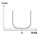
- FIG. 1 It is a figure which shows schematic structure of the antenna device which concerns on the 4th modification of the 1st Embodiment of this invention. It is a figure which shows schematic structure of the antenna device which concerns on the 5th modification of the 1st Embodiment of this invention. It is a figure which shows schematic structure of the antenna device which concerns on the 6th modification of the 1st Embodiment of this invention. It is a figure which shows schematic structure of the antenna device which concerns on the 7th modification of the 1st Embodiment of this invention. It is a figure which shows schematic structure of the antenna device which concerns on the 8th modification of the 1st Embodiment of this invention. 4 is a graph schematically showing frequency characteristics of VSWR of the antenna device of FIG. 1.
- FIG. 12 is a graph schematically showing frequency characteristics of VSWR of the antenna device of FIG. 11. It is a figure which shows schematic structure of the antenna device which concerns on the 9th modification of the 1st Embodiment of this invention. It is a figure which shows schematic structure of the antenna device which concerns on the 10th modification of the 1st Embodiment of this invention. It is a figure which shows schematic structure of the antenna device which concerns on the 11th modification of the 1st Embodiment of this invention. It is a figure which shows schematic structure of the antenna device which concerns on the 12th modification of the 1st Embodiment of this invention. It is a figure which shows schematic structure of the antenna device which concerns on the 13th modification of the 1st Embodiment of this invention.
- FIG. 20 is a circuit diagram equivalently showing a first embodiment of the electromagnetic coupling adjusting element D1 of FIG. 19.
- FIG. 20 is a circuit diagram equivalently showing a second embodiment of the electromagnetic coupling adjusting element D ⁇ b> 1 of FIG. 19.
- FIG. 20 is a circuit diagram equivalently showing a third embodiment of the electromagnetic coupling adjusting element D ⁇ b> 1 of FIG. 19.
- FIG. 20 is a circuit diagram equivalently showing a fourth embodiment of the electromagnetic coupling adjusting element D ⁇ b> 1 of FIG. 19.
- FIG. 35 is a circuit diagram showing a first example of electromagnetic coupling adjusting elements D1, D2 of FIG. 34.
- FIG. 52 is a circuit diagram equivalently showing an electromagnetic coupling adjusting element D1 of FIG. 51.
- 52 is a graph showing electromagnetic coupling between antenna elements A1 and A2 of the antenna apparatus of FIG. 51.
- FIG. 55 is a circuit diagram equivalently showing the electromagnetic coupling adjusting element D1 of FIG. 54.
- 57 is a graph showing electromagnetic coupling between antenna elements A111 and A112 of the antenna device of FIG. It is a graph which shows the radiation efficiency of the antenna apparatus of FIG.51 and FIG.54.
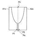
- FIG. 1 is a diagram illustrating a schematic configuration of an antenna device according to a first embodiment of the present invention.
- the antenna device of the present embodiment includes a ground conductor G1 made of a conductor plate and two antenna elements A1 and A2 each made of a conductor plate.
- the ground conductor G1 and the antenna elements A1 and A2 are provided, for example, in the same plane.
- Each antenna element A1, A2 has a first reference along a virtual reference axis (indicated by a vertical dotted line in FIG. 1) passing through the first reference point Pa and the second reference point Pb of the antenna device. It is provided so as to be close to the section between the point Pa and the second reference point Pb.
- Each of the antenna elements A1 and A2 includes a first portion that is close to the reference axis and electromagnetically coupled to the other antenna element along the circumference of the antenna element, and a second portion that is remote from the reference axis.
- the first portions of the antenna elements A1 and A2 are closest to each other in the vicinity of the first reference point Pa, and the antenna elements A1 and A2 move in the direction from the first reference point Pa to the second reference point Pb. It has a shape (tapered shape) in which the distance between A2 gradually increases.
- the antenna device includes feeding points P1 and P2 provided in the antenna elements A1 and A2 in the vicinity of the first reference point Pa, respectively.
- the feeding points P1 and P2 are preferably provided close to the reference axis, respectively.
- a power feeding unit including the power feeding points P1 and P2 is provided.
- the first signal source Q1 is connected to the feed point P1 on the antenna element A1 and the ground point P3 on the ground conductor G1, and the feed point P2 on the antenna element A2 and the ground point P4 on the ground conductor G1.
- Each antenna element A1, A2 can simultaneously transmit (or receive) different radio signals (for example, radio signals of a plurality of substreams of MIMO communication) by being excited through the feed points P1, P2. .
- the antenna apparatus can operate while ensuring isolation between the antenna elements A1 and A2.
- the radiation direction of the antenna device is, for example, a direction from a portion closest to each other between the antenna elements A1 and A2 toward the tapered opening (that is, a direction from the first reference point Pa to the second reference point Pb). .
- FIG. 2 is a diagram showing a current path of the antenna device of FIG.
- the length from the feeding point P1 of the antenna element A1 to the end point P5 on the radial direction side of the antenna element A1 is, for example, for the operating wavelength ⁇
- the length from the feeding point P2 of the antenna element A2 to the end point P6 on the radial direction side of the antenna element A2 is also configured to be, for example, a length of about ⁇ / 4.
- the current path of FIG. 2 shows a case where only the signal source Q1 is operated and the signal source Q2 is not operated (thus, the signal source Q2 is shown as a load in FIG. 2).
- the current I1 flows in the first part (the part close to the reference line) of the antenna element A1, and the second part (reference line) of the antenna element A1.
- the current I3 flows to the part remote from.
- electromagnetic coupling occurs between the antenna elements A1 and A2, and a back electromotive force V2 is generated at the feeding point P2. Therefore, a current I2 having a phase opposite to that of the current I1 of the antenna element A1 flows through the antenna element A2.
- the distance between the antenna elements A1 and A2 gradually increases from the first reference point Pa to the second reference point Pb as it goes in the direction from the first reference point Pa to the second reference point Pb.
- the electromagnetic coupling between the antenna elements A1 and A2 gradually decreases in the direction toward the reference point Pb. For this reason, the currents I1 and I2 are easily radiated partially into the space.
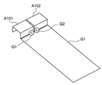
- FIG. 3 is a diagram illustrating a schematic configuration and a current path of an antenna device according to a comparative example.
- the antenna device of FIG. 3 includes antenna elements A101 and A102 each formed of a rectangular conductor plate, and the antenna elements A101 and A102 are close to each other with a certain distance therebetween.
- a current I2 flows through the antenna element A2. At this time, the intensity of the currents I1 and I2 is maximized in the vicinity of the feeding points P1 and P2.
- the antenna device of FIG. 1 can achieve good radiation while generating the currents I1 and I2 having opposite phases.
- the antenna apparatus of this embodiment operate
- the antenna device of this embodiment can operate while ensuring isolation between the antenna elements A1 and A2.
- a portion where the distance between the antenna elements A1 and A2 gradually increases in the first portion of the antenna elements A1 and A2 is shown in a curved shape, but this portion may be a straight line, or at least a portion. In particular, it may include a curve and / or a straight line.
- the ground conductor G1 is shown as a rectangular conductor plate in FIG. 1, the ground conductor G1 is not limited to a rectangle, and may be another polygon, a circle, an ellipse, or the like. Further, the antenna elements A1 and A2 and the ground conductor G1 need not be provided in the same plane.
- the radiation direction of the antenna device is shown to coincide with the direction from the first reference point Pa to the second reference point Pb, but the radiation characteristics of the antenna device are limited to this. It may have other radial directions.
- FIG. 4 is a diagram showing a schematic configuration and a current path of an antenna device according to a first modification of the first embodiment of the present invention
- FIG. 5 is a second diagram of the first embodiment of the present invention. It is a figure which shows schematic structure and the current pathway of the antenna apparatus which concerns on a modification.
- the feeding points P1 and P2 may be provided with a predetermined distance from the reference axis instead of being close to the reference axis. As shown in FIG. 1, when the feeding points P1 and P2 are provided close to the reference axis, the phases of the currents I1 and I2 (see FIG. 2) are almost opposite to each other, so that the antenna device is a tapered slot antenna.
- FIG. 4 shows a case where the feeding points P1, P2 are provided with a larger distance from the reference axis than in the case of FIG. 1
- FIG. 5 shows the feeding points P1, P2 from the reference axis of FIG. The case where it is provided with a larger distance than the case is shown.
- the antenna device is downsized.
- the distance from the reference axis to the feeding points P1 and P2 can be designed to be optimal at the target frequency in consideration of the trade-off between isolation and matching.
- FIG. 6 to 9 are diagrams showing a schematic configuration of the antenna device according to the third to sixth modifications of the first embodiment of the present invention.
- the length of the portion where the distance between the antenna elements A1a and A2a gradually increases in the first portion of the antenna elements A1a and A2a is the same as that of the antenna device of FIG. Accordingly, the distance between the antenna elements A1a and A2a increases more rapidly than in the antenna device of FIG.
- the length of the portion where the antenna elements A1a and A2a are parallel to each other in the first portion of the antenna elements A1a and A2a is increased. Further, in the antenna device of FIG.
- each antenna element A1, A2 is configured to spread at a steep angle as it goes from the first reference point Pa to the second reference point Pb.
- each antenna element A1c, A2c is configured to gradually spread in the direction from the first reference point Pa to the second reference point Pb.
- the antenna elements A1d and A2d are extended in the direction from the second reference point Pb to the first reference point Pa, and the antenna elements A1d and A2d are connected between the antenna elements A1d and A2d.
- the distance between the antenna elements A1 and A2 gradually increases from the closest part to the direction of the first reference point Pa. According to the antenna device of FIG. 9, the path length of the current flowing through the antenna elements A1d and A2d can be increased, and an operation at a lower frequency can be realized. 6 to 9 can provide the same effects as the antenna device of FIG.
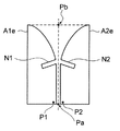
- FIG. 10 is a diagram showing a schematic configuration of an antenna device according to a seventh modification of the first embodiment of the present invention.
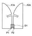
- slits N1 and N2 are provided in the first portions (portions close to the reference line) of the antenna elements A1e and A2e.
- the path length of the current flowing through the antenna elements A1e and A2e can be increased, and an operation at a lower frequency can be realized.
- a plurality of slits (called corrugates) may be provided for each antenna element. In this case, the operating frequency can be further lowered than when one slit is provided.
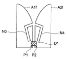
- FIG. 11 is a diagram showing a schematic configuration of an antenna apparatus according to an eighth modification of the first embodiment of the present invention.
- 12 is a graph schematically showing the frequency characteristics of the VSWR of the antenna device of FIG. 1
- FIG. 13 is a graph schematically showing the frequency characteristics of the VSWR of the antenna device of FIG.
- the antenna device of FIG. 11 replaces the slits N1 and N2 of FIG. 10 with slits N3 and N4 having portions extending toward the feed points P1 and P2 as first portions (reference lines) of the antenna elements A1f and A2f. In the vicinity of the).
- the slit lengths of the slits N3 and N4 are configured to be ⁇ / 4 with respect to the operating wavelength ⁇ .
- the slits N1 and N2 are provided in the first portions of the antenna elements A1e and A2e to increase the path length of the current flowing through the antenna elements A1e and A2e. Realized the operation. According to the antenna device of FIG. 11, band blocking is realized at the frequency f0 at which the slit lengths of the slits N3 and N4 are ⁇ / 4, and there is an effect that unnecessary radiation can be suppressed.
- each antenna element in FIGS. 6 to 11 may be combined.
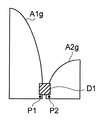
- FIG. 14 is a diagram showing a schematic configuration of an antenna device according to a ninth modification of the first embodiment of the present invention.
- the antenna elements A1 and A2 are shown to be symmetric with respect to the reference axis, but the embodiment of the present invention is not limited to this.
- the antenna elements A1g and A2g have different shapes, and the antenna elements A1g and A2g are asymmetric with respect to the reference axis.
- the radiation pattern of each antenna element A1g and A2g is made asymmetric, and the correlation between the radio signals transmitted and received from each antenna element A1g and A2g is reduced three-dimensionally. It becomes possible to do.
- FIG. 15 is a diagram showing a schematic configuration of an antenna apparatus according to a tenth modification of the first embodiment of the present invention.
- the antenna device of FIG. 15 is configured as a plate-like inverted F-type antenna device.
- the antenna elements A1 and A2 and the ground conductor G1 are provided in parallel with a predetermined distance apart so as to overlap each other.
- short-circuit conductors 31 and 32 are connected between the antenna elements A1 and A2 and the ground conductor G1, respectively.
- the short-circuit conductors 31 and 32 are necessary for impedance adjustment, but may be unnecessary depending on the configuration of the antenna device.
- FIG. 16 is a diagram showing a schematic configuration of an antenna apparatus according to an eleventh modification of the first embodiment of the present invention.
- the ground conductor is not limited to a single conductor plate as in the antenna device of FIG.
- the antenna device of FIG. 16 includes a ground conductor G2 corresponding to the antenna element A1 and a ground conductor G3 corresponding to the antenna element A2 instead of the ground conductor G1 of FIG. 1, and includes the antenna element A1 and the ground conductor G2.
- the dipole antenna is configured as a dipole antenna including an antenna element A2 and a ground conductor G3.
- the ground conductors G2 and G3 are each a conductor plate.
- the third reference point Pc is located on the side opposite to the second reference point Pb with respect to the first reference point Pa. deep.
- Each of the ground conductors G2 and G3 is provided so as to be close to a section between the first reference point Pa and the third reference point Pc along the reference axis.
- Each of the ground conductors G2 and G3 includes a first portion that is close to the reference axis and electromagnetically coupled to the other ground conductor along the circumference of the ground conductor, and a second portion that is remote from the reference axis.
- the first portions of the ground conductors G2 and G3 are closest to each other in the vicinity of the first reference point Pa, and the ground conductors G2 and G3 approach the direction from the first reference point Pa to the third reference point Pc. It has a shape (tapered shape) in which the distance between G3 gradually increases.
- the ground conductors G2 and G3 are shown to be symmetric with respect to the reference axis, but the embodiment of the present invention is not limited to this.
- FIG. 17 is a diagram showing a schematic configuration of an antenna device according to a twelfth modification of the first embodiment of the present invention.
- the embodiment of the present invention is not limited to the configuration including two antenna elements as described above, and may include three or more antenna elements.
- the antenna device of FIG. 17 shows a case where four antenna elements A11 to A14 are provided.
- the antenna device of FIG. 17 includes a ground conductor G1 made of a conductor plate and antenna elements A11 to A14 made of conductor plates provided vertically on the ground conductor G1.
- Each of the antenna elements A11 to A14 has a first reference along a virtual reference axis (indicated by a vertical dotted line in FIG. 1) passing through the first reference point Pa and the second reference point Pb of the antenna device.
- Each of the antenna elements A11 to A14 includes a first portion that is close to the reference axis and electromagnetically coupled to another antenna element along the circumference of the antenna element, and a second portion that is remote from the reference axis.
- the first portions of the antenna elements A11 to A14 are closest to each other in the vicinity of the first reference point Pa, and the antenna elements A11 to A14 are moved toward the second reference point Pb from the first reference point Pa.
- the distance between A14 gradually increases (tapered shape).
- the antenna device includes feed points (not shown) provided in the antenna elements A11 to A14 in the vicinity of the first reference point Pa.
- the feeding points are preferably provided close to the reference axis, respectively.
- the antenna elements A11 to A14 are provided along the reference axis, preferably at an angle of 90 degrees with each other. According to the antenna device of the present embodiment, communication speed can be increased by increasing the number of antenna elements.
- FIG. 18 is a diagram showing a schematic configuration of an antenna apparatus according to a thirteenth modification of the first embodiment of the present invention.
- the antenna device of FIG. 18 shows a case where six antenna elements A21 to A26 are provided.
- the antenna elements A21 to A26 are provided along the reference axis, preferably at an angle of 60 degrees with respect to each other.
- the antenna device of the present embodiment is not limited to the configuration including two, four, or six antenna elements, and may include other numbers of antenna elements.
- the antenna elements A11 to A14 and A21 to A26 are shown to have the same shape as the antenna elements A1 and A2 in FIG. 1, but for example, those shown in FIGS. An antenna element having another shape such as the above may be used.
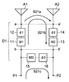
- FIG. 19 is a diagram showing a schematic configuration of an antenna apparatus according to the second embodiment of the present invention.
- the antenna device of the present embodiment is provided so that the antenna elements A1 and A2 are connected to each other in the first portions (portions close to the reference line) of the antenna elements A1 and A2.
- an electromagnetic coupling adjusting element D1 for adjusting the electromagnetic coupling between the antenna elements A1 and A2 in a predetermined frequency band.
- the electromagnetic coupling adjustment element D1 performs electromagnetic coupling between the antenna elements A1 and A2.
- a current path is formed through which a current that substantially cancels the current flowing through (or antenna element A1) flows.
- the electromagnetic coupling between the antenna elements A1 and A2 can be reduced by the current flowing through the electromagnetic coupling adjusting element D1.
- the isolation between the antenna elements A1 and A2 can be further improved by providing the electromagnetic coupling adjusting element D1.
- FIG. 20 is a diagram showing a current path of the antenna device of FIG.
- the current path in FIG. 20 shows a case where only the signal source Q1 is operated and the signal source Q2 is not operated (thus, the signal source Q2 is shown as a load in FIG. 20).
- the current I1 flows through the first part of the antenna element A1 (the part close to the reference line), and the second part of the antenna element A1 (the part remote from the reference line).
- a current I3 flows.
- electromagnetic coupling occurs between the antenna elements A1 and A2, and a back electromotive force V2 is generated at the feeding point P2.
- the electromagnetic coupling adjustment element D1 is connected to the electromagnetic coupling adjustment element D1 from the feeding point P2 in order to cancel the electromagnetic coupling between the antenna elements A1 and A2.
- Current flowing through the feeding point P1 is generated.
- the electromagnetic coupling adjusting element D1 when both signal sources Q1 and Q2 are operated, the electromagnetic coupling adjusting element D1 generates a current for canceling the electromagnetic coupling between the antenna elements A1 and A2.
- 21 to 24 show some embodiments of the electromagnetic coupling adjusting element D1 shown in FIG.
- FIG. 21 is a circuit diagram equivalently showing a first embodiment of the electromagnetic coupling adjusting element D1 of FIG.
- the electromagnetic coupling adjusting element D1 of FIG. 21 is a low coupling circuit composed of a plurality of susceptance elements (circuit elements having predetermined susceptance values b1 to b9) 1 to 9, and is suitable for miniaturization.
- the electromagnetic coupling adjusting element D1 can be made highly efficient.
- the electromagnetic coupling adjusting element D1 generates a current for canceling the electromagnetic coupling between the antenna elements A1 and A2.
- the circuit may be opened instead of the susceptance elements 1 to 9. In this case, the manufacturing cost of the antenna device can be reduced by reducing the number of circuit elements.
- FIG. 22 is a circuit diagram equivalently showing a second embodiment of the electromagnetic coupling adjusting element D1 of FIG.
- the electromagnetic coupling adjusting element D1 is not limited to the low coupling circuit composed of the susceptance elements 1 to 9.
- the amplitude adjusters 11, 13, 15 and the phase shifters 12, 14 are used. , 16 is also possible.
- the current path from the feeding point P1 to the feeding point P2 is the current path via the electromagnetic coupling between the antenna elements A1 and A2, and the current via the amplitude adjuster 15 and the phase shifter 16. Includes two routes.
- the amplitudes M1, M2, M3 of the amplitude adjusters 11, 13, 15 and the phase shift amounts ⁇ 1, ⁇ 2, of the phase shifters 12, 14, 16, respectively. Adjust ⁇ 3.
- the condition is that the transmission coefficient between the antenna elements A1 and A2 above the reference line aa ′ in FIG. 22 is S21a, and the transmission coefficient between the antenna elements A1 and A2 above the reference line bb ′ in FIG. Is S21b, and the transmission coefficient between the feeding points P1 and P2 passing through the amplitude adjuster 15 and the phase shifter 16 is S21c, it is calculated by the following procedure.
- each mathematical expression is referred to by a number in parentheses described after the mathematical expression.
- the transmission coefficient S21a between the antenna elements A1 and A2 is expressed by the following equation (1) with a predetermined amplitude M and a predetermined phase shift amount ⁇ .
- the transmission coefficients S21b, S21c are represented by the following formulas (2) and (3).
- FIG. 23 is a circuit diagram equivalently showing the third embodiment of the electromagnetic coupling adjusting element D1 of FIG. 19, and FIG. 24 equivalently shows the fourth embodiment of the electromagnetic coupling adjusting element D1 of FIG. FIG.
- the electromagnetic coupling adjusting element D1 of FIG. 22 may be simplified as shown in FIG.
- a circuit equivalent to the electromagnetic coupling adjusting element D1 in FIG. 23 may be configured using the conductive element 21 in FIG. 24 instead of the amplitude adjuster 15 and the phase shifter 16 in FIG. 24, the phase can be changed by changing the electrical length d of the conductive element 21, and the amplitude can be changed by changing the width w of the conductive element 21. is there.
- the configuration using the conductive element 21 is not applicable to all antenna devices, there is an effect that the structure is simple and the manufacture is easy.
- the antenna elements A1, A2 and the conductive element 21 may be integrally formed from a single conductor plate.
- the electromagnetic coupling adjusting element D1 generates a current for canceling the electromagnetic coupling between the antenna elements A1 and A2.
- the electromagnetic coupling adjusting element D1 in FIGS. 21 to 24 may be used in combination.
- the correlation coefficient (rho) (refer nonpatent literature 1) defined by the following formula
- the antenna apparatus of the present embodiment can efficiently transmit and receive a plurality of wideband radio signals having low correlation with each other simultaneously.
- FIGS. 25 to 33 are diagrams showing a schematic configuration of the antenna device according to the first to ninth modifications of the second embodiment of the present invention.
- the antenna device of FIGS. 25 to 33 has a configuration in which an electromagnetic coupling adjusting element D1 is added to the antenna devices of FIGS. 6 to 11 and FIGS.
- the isolation between the antenna elements A1 and A2 can be further improved as compared with the case of the first embodiment.
- FIG. 34 is a diagram showing a schematic configuration of an antenna apparatus according to a tenth modification of the second embodiment of the present invention.
- the electromagnetic coupling adjusting element that adjusts the electromagnetic coupling between the antenna elements A1 and A2 is not limited to one, and the antenna device in FIG. 34 has an electromagnetic wave between the antenna elements A1 and A2 in addition to the configuration of the antenna device in FIG.
- An additional electromagnetic coupling adjusting element D2 for adjusting the coupling is further provided.
- the electromagnetic coupling adjustment element D2 has feeding points P1 and P2 that are more than the electromagnetic coupling adjustment element D1 so that the antenna elements A1 and A2 are connected to each other in the first parts (parts close to the reference line) of the antenna elements A1 and A2. Provided away from.
- the electromagnetic coupling adjusting element D2 is connected to the feeding point P1 on the antenna element A1 (or the feeding point P2 on the antenna element A2) in a frequency band lower than the frequency band when the current path passing through the electromagnetic coupling adjusting element D1 is formed.
- a current path is formed through which a current Id2 that substantially cancels the current flowing through the antenna element A2 (or the antenna element A1) flows due to electromagnetic coupling between the antenna elements A1 and A2. Therefore, the antenna device of FIG. 34 includes a plurality of electromagnetic coupling adjusting elements D1 and D2, thereby forming a current path between the antenna elements A1 and A2 in different frequency bands, and each of the electromagnetic coupling adjusting elements D1 and D2 being connected. With the flowing currents Id1 and Id2, electromagnetic coupling between the antenna elements A1 and A2 can be reduced (multiband) in different frequency bands.
- FIG. 35 is a circuit diagram showing a first embodiment of the electromagnetic coupling adjusting elements D1, D2 of FIG.
- a resonant circuit using an inductor L and a capacitor C is considered as the electromagnetic coupling adjusting elements D1 and D2.
- the electromagnetic coupling adjusting element D1 allows only the current of the frequency f1 to flow by setting the circuit element value so as to pass the current of the frequency f1 and not pass the current of the frequency f2 lower than the frequency f1.
- the electromagnetic coupling adjusting element D2 can select and flow only the current of the frequency f2 by setting the circuit element value so as to pass the current of the frequency f2 and not pass the current of the frequency f1. is there.
- FIG. 36 to 38 are graphs showing a second embodiment of the electromagnetic coupling adjusting elements D1 and D2 in FIG.
- Examples of the electromagnetic coupling adjusting elements D1 and D2 are not limited to the circuit of FIG. 35, and a plurality of filters may be combined as shown in the graphs of FIGS.
- FIG. 36 shows a case where the electromagnetic coupling adjusting elements D1 and D2 are configured as band pass filters.
- the electromagnetic coupling adjusting element D1 passes the current of the frequency f1 and blocks the current of the frequency f2, and the electromagnetic coupling adjusting element D2 passes the current at frequency f2 and blocks the current at frequency f1.
- FIG. 37 shows a case where the electromagnetic coupling adjusting elements D1 and D2 are configured as a band rejection filter.
- the electromagnetic coupling adjusting element D1 blocks the current of the frequency f3 and passes the current of the frequency f4 higher than the frequency f3. Then, the electromagnetic coupling adjusting element D2 blocks the current having the frequency f4 and allows the current having the frequency f3 to pass.
- FIG. 38 shows a case where the electromagnetic coupling adjustment element D1 is configured as a high-pass filter and the electromagnetic coupling adjustment element D2 is configured as a low-pass filter.
- the electromagnetic coupling adjustment element D1 passes a current having a frequency f6.
- the current of the frequency f5 lower than the frequency f6 is blocked, and the electromagnetic coupling adjusting element D2 passes the current of the frequency f5 and blocks the current of the frequency f6 or higher.
- the number of electromagnetic coupling adjusting elements is not limited to two, and three or more electromagnetic coupling adjusting elements may be provided similarly.
- FIG. 39 is a diagram showing a schematic configuration of an antenna apparatus according to an eleventh modification of the second embodiment of the present invention.
- the antenna device of FIG. 39 is provided so that the antenna elements A11 to A14 are connected to each other in the first portions (portions close to the reference line) of the antenna elements A11 to A14.
- an electromagnetic coupling adjusting element D3 for adjusting electromagnetic coupling between the antenna elements A11 to A14 in a predetermined frequency band.
- the electromagnetic coupling adjusting element D3 supplies power to the feeding point of the first antenna element in a predetermined frequency band between any pair of the first and second antenna elements of the antenna elements A11 to A14, A current path through which a current that substantially cancels the current flowing through the second antenna element is caused to flow by electromagnetic coupling between the first and second antenna elements.
- the electromagnetic coupling between the antenna elements A11 to A14 can be reduced by the current flowing through the electromagnetic coupling adjusting element D3.
- the isolation between the antenna elements A11 to A14 can be further improved as compared with the antenna device of FIG.
- FIG. 40 is a diagram showing a schematic configuration of an antenna apparatus according to a twelfth modification of the second embodiment of the present invention.
- the antenna device of FIG. 40 is provided so that the antenna elements A21 to A26 are connected to each other in the first portions (portions close to the reference line) of the antenna elements A21 to A26.
- an electromagnetic coupling adjusting element D4 for adjusting electromagnetic coupling between the antenna elements A21 to A26 in a predetermined frequency band.
- the electromagnetic coupling adjusting element D4 is provided, so that the isolation between the antenna elements A21 to A26 can be further improved as compared with the antenna device of FIG.
- FIG. 41 simulation results of the antenna device according to the first embodiment of the present invention will be described with reference to FIGS. 41 to 50.
- FIG. 41 is a development view showing a schematic configuration of the antenna device according to the first comparative example
- FIG. 42 is a perspective view showing a schematic configuration of the antenna device of FIG.
- the antenna device of FIG. 41 corresponds to the antenna device according to the comparative example of FIG. In this simulation, the antenna device of FIG. 41 is bent along the dotted lines on the antenna elements A101 and A102 and configured as shown in FIG. Thereby, the antenna device can be reduced in size.
- FIG. 43 is a graph showing the reflection coefficient S11 and the transmission coefficient S21 of the antenna device of FIG. In order to ensure isolation, the transmission coefficient S21 is desirably ⁇ 10 dB or less. Referring to FIG. 43, it can be seen that the antenna device of FIG. 41 does not achieve a sufficient reduction in the transmission coefficient S21.
- FIG. 44 is a diagram showing a schematic configuration of the antenna device according to the first embodiment of the present invention
- FIG. 45 is a perspective view showing a schematic configuration of the antenna device of FIG.
- the antenna device of FIG. 44 corresponds to the antenna device of FIG.
- the antenna device of FIG. 44 was bent along the dotted lines on the antenna elements A1b and A2b, and configured as shown in FIG.
- FIG. 46 is a graph showing the reflection coefficient S11 and the transmission coefficient S21 of the antenna device of FIG. Referring to FIG. 46, it can be seen that the transmission coefficient S21 can be reduced over a wide band in the antenna apparatus of FIG. 44 compared to the antenna apparatus of FIG.
- FIG. 47 is a diagram showing a schematic configuration of an antenna apparatus according to a second embodiment of the present invention
- FIG. 48 is a perspective view showing a schematic configuration of the antenna apparatus of FIG.
- the antenna device of FIG. 47 corresponds to the antenna device of FIG. In this simulation, the antenna device of FIG. 47 was bent along the dotted lines on the antenna elements A1 and A2, and configured as shown in FIG.
- FIG. 49 is a graph showing the reflection coefficient S11 and the transmission coefficient S21 of the antenna device of FIG. Referring to FIG. 48, it can be seen that the antenna apparatus of FIG. 47 can also reduce the transmission coefficient S21 over a wide band compared to the antenna apparatus of FIG. Furthermore, it can be seen that the antenna apparatus of FIG.
- FIG. 50 is a table showing the radiation efficiency of the antenna device of FIGS. 41, 44, and 47.
- the unit is dB.
- the thick line column in the first embodiment (FIG. 44) and the second embodiment (FIG. 47) shows the operating frequency at which higher radiation efficiency was obtained than in the first comparative example (FIG. 41). .
- the antenna device of the example of the present invention can improve the radiation efficiency over a wide band as compared with the antenna device of the first comparative example.
- the radiation efficiency is improved by reducing the transmission coefficient S21
- the radiation efficiency is improved by reducing the transmission coefficient S21 and the reflection coefficient S11.
- the antenna device according to the embodiment of the present invention can be operated as a wideband antenna device that can secure and provide isolation between antenna elements and can simultaneously transmit and receive a plurality of wideband wireless signals, while having a small and simple configuration. is there.
- FIG. 51 is a diagram showing a schematic configuration of an antenna apparatus according to a third embodiment of the present invention.
- the antenna device of FIG. 51 corresponds to the antenna device of FIG.
- the antenna elements A1 and A2 are 27 ⁇ 90 mm in size, the ground conductor G1 is 57 ⁇ 90 mm in size, and the antenna elements A1 and A2 are 1 mm from the ground conductor G1 in the same plane as the ground conductor G1. They are spaced apart.
- the antenna elements A1 and A2 have a tapered shape such that the distance between the antenna elements A1 and A2 gradually increases.
- FIG. 52 is a circuit diagram equivalently showing the electromagnetic coupling adjusting element D1 of FIG.
- the electromagnetic coupling adjusting element D1 in FIG. 52 is designed so that electromagnetic coupling between the antenna elements A1 and A2 is reduced at 1000 MHz.
- FIG. 54 is a diagram showing a schematic configuration of the antenna device of the second comparative example.
- the antenna device of FIG. 51 is a wideband model (Wideband Model), whereas the antenna device of FIG. 54 is a narrowband model (Narrowband Model) in which antenna elements as shown in Patent Document 1 are arranged in parallel to each other. ).
- the antenna elements A111 and A112 are 2 ⁇ 90 mm in size, the ground conductor G1 is 57 ⁇ 90 mm in size, and the antenna elements A111 and A112 are 1 mm from the ground conductor G1 in the same plane as the ground conductor G1. They are spaced apart.
- FIG. 55 is a circuit diagram equivalently showing the electromagnetic coupling adjusting element D1 of FIG.
- the electromagnetic coupling adjusting element D1 in FIG. 55 is designed so that the electromagnetic coupling between the antenna elements A111 and A112 is reduced at 1000 MHz.
- FIG. 53 is a graph showing the electromagnetic coupling between the antenna elements A1 and A2 of the antenna apparatus of FIG. 51
- FIG. 56 is a graph showing the electromagnetic coupling between the antenna elements A111 and A112 of the antenna apparatus of FIG. 53 and 56 show the transmission coefficient S21 between the feeding points P1 and P2 with respect to the frequency.
- the transmission coefficient S21 is ⁇ 5 dB or more at 1000 MHz in any result. It shows a high value.
- the transmission coefficient S21 can be reduced to ⁇ 10 dB or less at 1000 MHz in any result.
- the antenna device of the second comparative example is 6 MHz
- the antenna device of the third embodiment secures 260 MHz or more. It can be seen that the third embodiment is 43 times wider.
- FIG. 57 is a graph showing the radiation efficiency of the antenna device of FIGS. It can be seen that both the antenna device of the third example and the antenna device of the second comparative example can maximize the radiation efficiency at 1000 MHz. However, when comparing the frequency bandwidth at which the radiation efficiency is 3 dB or more, the antenna device of the second comparative example is 64 MHz, whereas the antenna device of the third embodiment is 330 Hz, which is the third implementation. It can be seen that the example is 5 times wider.
- FIG. 58 is a graph showing the correlation coefficient of the antenna device of FIGS. It can be seen that both the antenna device of the third embodiment and the antenna device of the second comparative example can minimize the correlation coefficient at 1000 MHz. However, when comparing the frequency bandwidths where the correlation coefficient is 0.6 or less, the antenna device of the second comparative example is 14 MHz, whereas the antenna device of the third embodiment is 400 MHz. It can be seen that the third embodiment is 29 times wider.
- the present Example was designed so that the electromagnetic coupling between antenna element A1, A2 may be reduced in 1000 MHz, it is not restricted to this but can be applied also to another frequency.
- FIG. 59 is a diagram showing a schematic configuration of an antenna apparatus according to a fourth example of the first embodiment of the present invention.
- the antenna device of the present embodiment includes an example of the electromagnetic coupling adjustment element D1 of FIG. 24, and the antenna elements A1 and A2 and the electromagnetic coupling adjustment element D1 are integrally formed from a single conductor plate.
- FIG. 60 is a graph showing the reflection coefficient S11 and the transmission coefficient S21 of the antenna device of FIG. It can be seen that both the reflection coefficient S11 and the transmission coefficient S21 can be reduced to ⁇ 10 dB or less in the vicinity of 2100 to 2300 MHz.
- the antenna device of the present invention can be operated as a wideband antenna device that can secure and provide isolation between antenna elements and can simultaneously transmit and receive a plurality of wideband wireless signals, while having a small and simple configuration.
- the antenna device of the present invention and the wireless communication device using the antenna device can be mounted as a mobile phone, for example, or can be mounted as a device for a wireless LAN.
- This antenna device can be mounted on, for example, a wireless communication device for performing MIMO communication.
- the antenna device is not limited to MIMO, and an adaptive array antenna or maximum ratio capable of simultaneously executing communication for a plurality of applications (multi-application). It can also be mounted on an array antenna device such as a combined diversity antenna or a phased array antenna.
Abstract
Description
それぞれ周を有する導体板にてなる少なくとも2つのアンテナ素子を備えたアンテナ装置であって、
上記各アンテナ素子は、上記アンテナ装置の第1の位置と第2の位置とを通る基準軸に沿って、上記第1の位置と上記第2の位置との間の区間に近接するように設けられ、
上記各アンテナ素子は、当該アンテナ素子の周に沿って、上記基準軸に近接しかつ他のアンテナ素子に電磁的に結合した第1の部分と、上記基準軸から遠隔した第2の部分とを有し、
上記各アンテナ素子の上記第1の部分は、上記第1の位置の近傍において互いに最も近接し、上記第1の位置から上記第2の位置への方向に向かうにつれて上記各アンテナ素子間の距離が次第に増大する形状を有し、
上記アンテナ装置は、上記第1の位置の近傍において上記各アンテナ素子にそれぞれ設けられた給電点を備えたことを特徴とする。
上記2つのアンテナ素子は上記接地導体と同一平面内に設けられたことを特徴とする。
導体板にてなる接地導体と、
上記接地導体上に重なるように、上記接地導体から所定距離だけ離隔して平行に設けられた2つのアンテナ素子と、
上記2つのアンテナ素子を上記接地導体にそれぞれ接続する短絡導体とを備え、板状逆F型アンテナ装置として構成されたことを特徴とする。
上記各アンテナ素子は上記接地導体上に垂直に設けられたことを特徴とする。
上記電磁結合調整素子は、上記各アンテナ素子のうちの任意の一対の第1及び第2のアンテナ素子の間において、上記第1の周波数帯で上記第1のアンテナ素子の給電点に給電したときに上記第1及び第2のアンテナ素子間の電磁結合により上記第2のアンテナ素子に流れる電流を実質的に相殺する電流を流れさせる電流経路を形成することを特徴とする。
図1は、本発明の第1の実施形態に係るアンテナ装置の概略構成を示す図である。本実施形態のアンテナ装置は、導体板にてなる接地導体G1と、それぞれ導体板にてなる2つのアンテナ素子A1,A2とを備えている。接地導体G1とアンテナ素子A1,A2は、例えば同一平面内に設けられる。各アンテナ素子A1,A2は、アンテナ装置の第1の基準点Paと第2の基準点Pbとを通る仮想的な基準軸(図1において垂直な点線で示す)に沿って、第1の基準点Paと第2の基準点Pbとの間の区間に近接するように設けられる。アンテナ素子A1,A2のそれぞれは、当該アンテナ素子の周に沿って、基準軸に近接しかつ他方のアンテナ素子に電磁的に結合した第1の部分と、基準軸から遠隔した第2の部分とを有する。各アンテナ素子A1,A2の第1の部分は、第1の基準点Paの近傍において互いに最も近接し、第1の基準点Paから第2の基準点Pbへの方向に向かうにつれてアンテナ素子A1,A2間の距離が次第に増大する形状(テーパー形状)を有する。さらに、アンテナ装置は、第1の基準点Paの近傍において各アンテナ素子A1,A2にそれぞれ設けられた給電点P1,P2を備える。給電点P1,P2は、好ましくは、それぞれ基準軸に近接して設けられる。接地導体G1とアンテナ素子A1,A2とが対向した部分において、給電点P1,P2を含む給電部が設けられる。給電部において、アンテナ素子A1上の給電点P1と接地導体G1上の接地点P3とに第1の信号源Q1が接続され、アンテナ素子A2上の給電点P2と接地導体G1上の接地点P4とに第2の信号源Q2が接続される。各アンテナ素子A1,A2はそれぞれ、各給電点P1,P2を介して励振することにより異なる無線信号(例えば、MIMO通信の複数のサブストリームの無線信号)を同時に送信(又は受信)することができる。
図19は、本発明の第2の実施形態に係るアンテナ装置の概略構成を示す図である。本実施形態のアンテナ装置は、図1のアンテナ装置の構成に加えて、アンテナ素子A1,A2の第1の部分(基準線に近接した部分)においてアンテナ素子A1,A2を互いに接続するように設けられ、所定の周波数帯でアンテナ素子A1,A2間の電磁結合を調整する電磁結合調整素子D1を備える。電磁結合調整素子D1は、所定の周波数帯でアンテナ素子A1上の給電点P1(又はアンテナ素子A2上の給電点P2)に給電したときに,アンテナ素子A1,A2間の電磁結合によりアンテナ素子A2(又はアンテナ素子A1)に流れる電流を実質的に相殺する電流を流れさせる電流経路を形成する。この電磁結合調整素子D1を流れる電流により、アンテナ素子A1,A2間の電磁結合を低減することができる。本実施形態のアンテナ装置によれば、電磁結合調整素子D1を備えたことにより、アンテナ素子A1,A2間のアイソレーションをさらに向上させることができる。
=S21a×M1×M2×exp(j(φ1+φ2))
=M×M1×M2×exp(j(φ+φ1+φ2)) (2)

G1,G2,G3,G4…接地導体、
D1,D2,D3,D4…電磁結合調整素子、
I1,I3…アンテナ素子A1の電流、
I2…アンテナ素子A2の電流、
Id1…電磁結合調整素子D1の電流、
Id2…電磁結合調整素子D2の電流、
N1~N4…スリット、
Pa,Pb,Pc…基準点、
P1,P2…給電点、
P3,P4…接地点、
P5,P6…アンテナ素子A1,A2の放射方向側の端点、
Q1,Q2…信号源、
1~9…サセプタンス素子、
11,13,15…振幅調整器、
12,14,16…移相器、
21…導電性素子、
31,32…短絡導体。
Claims (21)
- それぞれ周を有する導体板にてなる少なくとも2つのアンテナ素子を備えたアンテナ装置であって、
上記各アンテナ素子は、上記アンテナ装置の第1の位置と第2の位置とを通る基準軸に沿って、上記第1の位置と上記第2の位置との間の区間に近接するように設けられ、
上記各アンテナ素子は、当該アンテナ素子の周に沿って、上記基準軸に近接しかつ他のアンテナ素子に電磁的に結合した第1の部分と、上記基準軸から遠隔した第2の部分とを有し、
上記各アンテナ素子の上記第1の部分は、上記第1の位置の近傍において互いに最も近接し、上記第1の位置から上記第2の位置への方向に向かうにつれて上記各アンテナ素子間の距離が次第に増大する形状を有し、
上記アンテナ装置は、上記第1の位置の近傍において上記各アンテナ素子にそれぞれ設けられた給電点を備えたことを特徴とするアンテナ装置。 - 上記各給電点はそれぞれ上記基準軸に近接して設けられたことを特徴とする請求項1記載のアンテナ装置。
- 上記各給電点はそれぞれ上記基準軸から所定距離を有して設けられたことを特徴とする請求項1記載のアンテナ装置。
- 上記各アンテナ素子はそれぞれ、上記各給電点を介して励振することにより異なる無線信号を同時に送信又は受信することを特徴とする請求項1~3のいずれか1つに記載のアンテナ装置。
- 上記各アンテナ素子は、上記基準軸に対して対称な形状を有することを特徴とする請求項1~4のいずれか1つに記載のアンテナ装置。
- 上記各アンテナ素子は、上記基準軸に対して非対称な形状を有することを特徴とする請求項1~4のいずれか1つに記載のアンテナ装置。
- 上記各アンテナ素子は、上記第1の部分においてスリットを有することを特徴とする請求項1~4のいずれか1つに記載のアンテナ装置。
- 上記各アンテナ素子において、上記スリットは上記給電点に向かって延在する部分を有することを特徴とする請求項7記載のアンテナ装置。
- 上記アンテナ装置は、2つのアンテナ素子と、導体板にてなる接地導体とを備え、
上記2つのアンテナ素子は上記接地導体と同一平面内に設けられたことを特徴とする請求項1~8のうちのいずれか1つに記載のアンテナ装置。 - 上記アンテナ装置は、
導体板にてなる接地導体と、
上記接地導体上に重なるように、上記接地導体から所定距離だけ離隔して平行に設けられた2つのアンテナ素子と、
上記2つのアンテナ素子を上記接地導体にそれぞれ接続する短絡導体とを備え、板状逆F型アンテナ装置として構成されたことを特徴とする請求項1~8のうちのいずれか1つに記載のアンテナ装置。 - 上記各アンテナ素子はダイポールアンテナであることを特徴とする請求項1~8のうちのいずれか1つに記載のアンテナ装置。
- 上記アンテナ装置は導体板にてなる接地導体を備え、
上記各アンテナ素子は上記接地導体上に垂直に設けられたことを特徴とする請求項1~8のうちのいずれか1つに記載のアンテナ装置。 - 上記各アンテナ素子は、少なくとも1カ所で折り曲げられていることを特徴とする請求項1~8のいずれか1つに記載のアンテナ装置。
- 上記アンテナ装置は、上記各アンテナ素子の上記第1の部分において上記各アンテナ素子を互いに接続するように設けられ、第1の周波数帯で上記各アンテナ素子間の電磁結合を調整する電磁結合調整素子をさらに備え、
上記電磁結合調整素子は、上記各アンテナ素子のうちの任意の一対の第1及び第2のアンテナ素子の間において、上記第1の周波数帯で上記第1のアンテナ素子の給電点に給電したときに上記第1及び第2のアンテナ素子間の電磁結合により上記第2のアンテナ素子に流れる電流を実質的に相殺する電流を流れさせる電流経路を形成することを特徴とする請求項1~13のうちのいずれか1つに記載のアンテナ装置。 - 上記電磁結合調整素子は、所定のサセプタンス値を有する複数の回路素子を含む低結合回路であることを特徴とする請求項14記載のアンテナ装置。
- 上記電磁結合調整素子は複数の振幅調整器及び複数の移相器を含むことを特徴とする請求項14記載のアンテナ装置。
- 上記電磁結合調整素子は導電性素子であることを特徴とする請求項14記載のアンテナ装置。
- 上記導電性素子は、上記各アンテナ素子と一体的に形成されたことを特徴とする請求項17記載のアンテナ装置。
- 上記電磁結合調整素子は、フィルタを含むことを特徴とする請求項14記載のアンテナ装置。
- 上記各アンテナ素子の上記第1の部分において上記各アンテナ素子を互いに接続するように設けられ、上記第1の周波数帯とは異なる周波数帯で上記各アンテナ素子間の電磁結合を調整する少なくとも1つの追加の電磁結合調整素子を備えたことを特徴とする請求項14~19のうちのいずれか1つに記載のアンテナ装置。
- 請求項1~20のうちのいずれか1つに記載のアンテナ装置を備えたことを特徴とする無線通信装置。
Priority Applications (4)
| Application Number | Priority Date | Filing Date | Title |
|---|---|---|---|
| CN2011800169832A CN102823060A (zh) | 2011-02-04 | 2011-10-28 | 天线装置及无线通信装置 |
| JP2012555578A JP5686823B2 (ja) | 2011-02-04 | 2011-10-28 | アンテナ装置及び無線通信装置 |
| US13/638,788 US20130021218A1 (en) | 2011-02-04 | 2011-10-28 | Antenna apparatus including multiple antenna elements for simultaneously transmitting or receiving multiple wideband radio signals |
| US14/747,014 US20150295322A1 (en) | 2011-02-04 | 2015-06-23 | Antenna apparatus including multiple antenna elements for simultaneously transmitting or receiving multiple wideband radio signals |
Applications Claiming Priority (2)
| Application Number | Priority Date | Filing Date | Title |
|---|---|---|---|
| JP2011-022278 | 2011-02-04 | ||
| JP2011022278 | 2011-02-04 |
Related Child Applications (2)
| Application Number | Title | Priority Date | Filing Date |
|---|---|---|---|
| US13/638,788 A-371-Of-International US20130021218A1 (en) | 2011-02-04 | 2011-10-28 | Antenna apparatus including multiple antenna elements for simultaneously transmitting or receiving multiple wideband radio signals |
| US14/747,014 Continuation US20150295322A1 (en) | 2011-02-04 | 2015-06-23 | Antenna apparatus including multiple antenna elements for simultaneously transmitting or receiving multiple wideband radio signals |
Publications (1)
| Publication Number | Publication Date |
|---|---|
| WO2012104941A1 true WO2012104941A1 (ja) | 2012-08-09 |
Family
ID=46602189
Family Applications (1)
| Application Number | Title | Priority Date | Filing Date |
|---|---|---|---|
| PCT/JP2011/006056 WO2012104941A1 (ja) | 2011-02-04 | 2011-10-28 | アンテナ装置及び無線通信装置 |
Country Status (4)
| Country | Link |
|---|---|
| US (2) | US20130021218A1 (ja) |
| JP (1) | JP5686823B2 (ja) |
| CN (1) | CN102823060A (ja) |
| WO (1) | WO2012104941A1 (ja) |
Cited By (6)
| Publication number | Priority date | Publication date | Assignee | Title |
|---|---|---|---|---|
| WO2013069186A1 (ja) * | 2011-11-11 | 2013-05-16 | パナソニック株式会社 | 非接触通信システムおよびダイポールアンテナ |
| JP2014112824A (ja) * | 2012-10-31 | 2014-06-19 | Murata Mfg Co Ltd | アンテナ装置 |
| JP2014179873A (ja) * | 2013-03-15 | 2014-09-25 | Nitto Denko Corp | アンテナモジュールおよびその製造方法 |
| WO2015182016A1 (ja) * | 2014-05-29 | 2015-12-03 | 株式会社東芝 | アンテナ装置、アンテナ装置の製造方法、及び無線装置 |
| JP2018511240A (ja) * | 2015-03-03 | 2018-04-19 | アメリカ合衆国 | 低交差偏波ディケード帯域幅の超広帯域アンテナ素子およびアレイ |
| WO2020027156A1 (ja) * | 2018-07-31 | 2020-02-06 | 株式会社ヨコオ | アンテナ装置 |
Families Citing this family (9)
| Publication number | Priority date | Publication date | Assignee | Title |
|---|---|---|---|---|
| EP2854318B1 (en) | 2012-05-22 | 2020-11-04 | Sun Patent Trust | Transmission method and transmission system |
| TWI536674B (zh) * | 2013-11-25 | 2016-06-01 | 智易科技股份有限公司 | 天線結構 |
| US10734728B2 (en) | 2015-08-27 | 2020-08-04 | Huawei Technologies Co., Ltd. | Antenna, antenna control method, antenna control apparatus, and antenna system |
| JP6272584B1 (ja) * | 2017-02-08 | 2018-01-31 | 三菱電機株式会社 | 減結合回路 |
| KR102188997B1 (ko) * | 2017-02-28 | 2020-12-09 | 동우 화인켐 주식회사 | 투명 필름 안테나 |
| US20200321713A1 (en) * | 2017-03-24 | 2020-10-08 | Huawei Technologies Co., Ltd. | Mimo antenna module |
| CN110612641B (zh) * | 2017-05-12 | 2021-06-25 | 瑞典爱立信有限公司 | 宽带天线 |
| KR102584427B1 (ko) * | 2018-11-20 | 2023-09-27 | 엘지전자 주식회사 | 무선 충전 장치 |
| CN110994121B (zh) * | 2019-10-23 | 2021-03-16 | 南京航空航天大学 | 一种用于混响室测量的超宽带混合天线 |
Citations (3)
| Publication number | Priority date | Publication date | Assignee | Title |
|---|---|---|---|---|
| JP2008199588A (ja) * | 2007-01-19 | 2008-08-28 | Matsushita Electric Ind Co Ltd | アレーアンテナ装置及び無線通信装置 |
| JP2009171096A (ja) * | 2008-01-15 | 2009-07-30 | Tdk Corp | 表面実装型アンテナおよびアンテナモジュール |
| JP2010028413A (ja) * | 2008-07-18 | 2010-02-04 | Panasonic Corp | 無線通信装置 |
Family Cites Families (6)
| Publication number | Priority date | Publication date | Assignee | Title |
|---|---|---|---|---|
| US6900770B2 (en) * | 2003-07-29 | 2005-05-31 | Bae Systems Information And Electronic Systems Integration Inc. | Combined ultra wideband Vivaldi notch/meander line loaded antenna |
| JP4555787B2 (ja) * | 2005-07-12 | 2010-10-06 | 日立電線株式会社 | アンテナ |
| FR2911725B1 (fr) * | 2007-01-24 | 2011-02-18 | Groupe Ecoles Telecomm | Antenne ou element d'antenne ultra-large bande. |
| JP2008258821A (ja) * | 2007-04-03 | 2008-10-23 | Nippon Soken Inc | アンテナモジュール |
| US7688273B2 (en) * | 2007-04-20 | 2010-03-30 | Skycross, Inc. | Multimode antenna structure |
| JP2011024176A (ja) * | 2009-07-14 | 2011-02-03 | Keycom Corp | 誘電体導波路の電磁波伝達部 |
-
2011
- 2011-10-28 US US13/638,788 patent/US20130021218A1/en not_active Abandoned
- 2011-10-28 CN CN2011800169832A patent/CN102823060A/zh active Pending
- 2011-10-28 WO PCT/JP2011/006056 patent/WO2012104941A1/ja active Application Filing
- 2011-10-28 JP JP2012555578A patent/JP5686823B2/ja active Active
-
2015
- 2015-06-23 US US14/747,014 patent/US20150295322A1/en not_active Abandoned
Patent Citations (3)
| Publication number | Priority date | Publication date | Assignee | Title |
|---|---|---|---|---|
| JP2008199588A (ja) * | 2007-01-19 | 2008-08-28 | Matsushita Electric Ind Co Ltd | アレーアンテナ装置及び無線通信装置 |
| JP2009171096A (ja) * | 2008-01-15 | 2009-07-30 | Tdk Corp | 表面実装型アンテナおよびアンテナモジュール |
| JP2010028413A (ja) * | 2008-07-18 | 2010-02-04 | Panasonic Corp | 無線通信装置 |
Cited By (13)
| Publication number | Priority date | Publication date | Assignee | Title |
|---|---|---|---|---|
| WO2013069186A1 (ja) * | 2011-11-11 | 2013-05-16 | パナソニック株式会社 | 非接触通信システムおよびダイポールアンテナ |
| JP2014112824A (ja) * | 2012-10-31 | 2014-06-19 | Murata Mfg Co Ltd | アンテナ装置 |
| JP2014179873A (ja) * | 2013-03-15 | 2014-09-25 | Nitto Denko Corp | アンテナモジュールおよびその製造方法 |
| US9553370B2 (en) | 2013-03-15 | 2017-01-24 | Nitto Denko Corporation | Antenna module and method for manufacturing the same |
| US10505260B2 (en) | 2014-05-29 | 2019-12-10 | Kabushiki Kaisha Toshiba | Antenna device, method of manufacturing antenna device, and wireless device |
| WO2015182016A1 (ja) * | 2014-05-29 | 2015-12-03 | 株式会社東芝 | アンテナ装置、アンテナ装置の製造方法、及び無線装置 |
| JPWO2015182016A1 (ja) * | 2014-05-29 | 2017-04-20 | 株式会社東芝 | アンテナ装置、アンテナ装置の製造方法、及び無線装置 |
| JP2018511240A (ja) * | 2015-03-03 | 2018-04-19 | アメリカ合衆国 | 低交差偏波ディケード帯域幅の超広帯域アンテナ素子およびアレイ |
| WO2020027156A1 (ja) * | 2018-07-31 | 2020-02-06 | 株式会社ヨコオ | アンテナ装置 |
| JPWO2020027156A1 (ja) * | 2018-07-31 | 2021-08-02 | 株式会社ヨコオ | アンテナ装置 |
| US11581659B2 (en) | 2018-07-31 | 2023-02-14 | Yokowo Co., Ltd. | Antenna device |
| JP7374097B2 (ja) | 2018-07-31 | 2023-11-06 | 株式会社ヨコオ | アンテナ装置 |
| US11862859B2 (en) | 2018-07-31 | 2024-01-02 | Yokowo Co., Ltd. | Antenna device |
Also Published As
| Publication number | Publication date |
|---|---|
| JPWO2012104941A1 (ja) | 2014-07-03 |
| US20130021218A1 (en) | 2013-01-24 |
| CN102823060A (zh) | 2012-12-12 |
| JP5686823B2 (ja) | 2015-03-18 |
| US20150295322A1 (en) | 2015-10-15 |
Similar Documents
| Publication | Publication Date | Title |
|---|---|---|
| JP5686823B2 (ja) | アンテナ装置及び無線通信装置 | |
| JP5826823B2 (ja) | アンテナ装置及び無線通信装置 | |
| US9680514B2 (en) | Methods for reducing near-field radiation and specific absorption rate (SAR) values in communications devices | |
| US20170244156A1 (en) | Multimode antenna structure | |
| US8742999B2 (en) | Antenna apparatus for simultaneously transmitting multiple radio signals with different radiation characteristics | |
| US7760150B2 (en) | Antenna assembly and wireless unit employing it | |
| WO2013061502A1 (ja) | アンテナ装置及び無線通信装置 | |
| WO2013008356A1 (ja) | アンテナ装置及び無線通信装置 | |
| JP5323271B2 (ja) | アンテナ装置及び無線通信装置 | |
| KR101727303B1 (ko) | 통신 장치에서 근거리 방사 및 전자파 흡수율값을 감소시키는 방법 | |
| WO2013175903A1 (ja) | アンテナ装置及びmimo無線装置 | |
| WO2014125832A1 (ja) | デュアルバンドアンテナ装置 | |
| JP2007300398A (ja) | マルチバンドアンテナおよびマルチバンドマルチアンテナ | |
| JP4910868B2 (ja) | アンテナ装置 | |
| JP2006140735A (ja) | 平面アンテナ | |
| US20200266545A1 (en) | Broad band dipole antenna | |
| WO2010138453A2 (en) | Methods for reducing near-field radiation and specific absorption rate (sar) values in communications devices | |
| JP2013093645A (ja) | アンテナ装置、及び無線通信装置 | |
| JP4881978B2 (ja) | アンテナ装置 | |
| JP2007215133A (ja) | ダイポールアンテナ及びマルチアンテナ装置 | |
| KR100581712B1 (ko) | 이동통신단말기용 링형 안테나 구조 |
Legal Events
| Date | Code | Title | Description |
|---|---|---|---|
| WWE | Wipo information: entry into national phase |
Ref document number: 201180016983.2 Country of ref document: CN |
|
| WWE | Wipo information: entry into national phase |
Ref document number: 2012555578 Country of ref document: JP |
|
| 121 | Ep: the epo has been informed by wipo that ep was designated in this application |
Ref document number: 11857600 Country of ref document: EP Kind code of ref document: A1 |
|
| WWE | Wipo information: entry into national phase |
Ref document number: 13638788 Country of ref document: US |
|
| NENP | Non-entry into the national phase |
Ref country code: DE |
|
| 122 | Ep: pct application non-entry in european phase |
Ref document number: 11857600 Country of ref document: EP Kind code of ref document: A1 |