WO2012101943A1 - マイクロアレイの解析方法および読取り装置 - Google Patents
マイクロアレイの解析方法および読取り装置 Download PDFInfo
- Publication number
- WO2012101943A1 WO2012101943A1 PCT/JP2011/080007 JP2011080007W WO2012101943A1 WO 2012101943 A1 WO2012101943 A1 WO 2012101943A1 JP 2011080007 W JP2011080007 W JP 2011080007W WO 2012101943 A1 WO2012101943 A1 WO 2012101943A1
- Authority
- WO
- WIPO (PCT)
- Prior art keywords
- microarray
- image data
- light
- fluorescence
- alignment
- Prior art date
Links
- 238000002493 microarray Methods 0.000 title claims abstract description 49
- 238000004458 analytical method Methods 0.000 title abstract description 36
- 238000000018 DNA microarray Methods 0.000 claims abstract description 85
- 239000000523 sample Substances 0.000 claims abstract description 81
- 239000000758 substrate Substances 0.000 claims abstract description 71
- 230000005284 excitation Effects 0.000 claims abstract description 55
- 238000000034 method Methods 0.000 claims abstract description 46
- 238000002073 fluorescence micrograph Methods 0.000 claims abstract description 45
- 238000010208 microarray analysis Methods 0.000 claims abstract description 16
- 230000001678 irradiating effect Effects 0.000 claims abstract description 6
- 238000003384 imaging method Methods 0.000 claims description 12
- 238000012937 correction Methods 0.000 claims description 8
- 230000003287 optical effect Effects 0.000 claims description 8
- 238000005259 measurement Methods 0.000 claims description 4
- 238000012545 processing Methods 0.000 abstract description 13
- 239000013641 positive control Substances 0.000 abstract description 8
- 238000001514 detection method Methods 0.000 description 20
- 108090000623 proteins and genes Proteins 0.000 description 20
- 230000008569 process Effects 0.000 description 13
- 239000007850 fluorescent dye Substances 0.000 description 12
- 102000004169 proteins and genes Human genes 0.000 description 11
- 230000007246 mechanism Effects 0.000 description 10
- 238000006243 chemical reaction Methods 0.000 description 6
- 150000001875 compounds Chemical class 0.000 description 6
- 238000010586 diagram Methods 0.000 description 6
- 238000009396 hybridization Methods 0.000 description 5
- 238000009739 binding Methods 0.000 description 4
- 230000014509 gene expression Effects 0.000 description 3
- 239000011521 glass Substances 0.000 description 3
- 239000011159 matrix material Substances 0.000 description 3
- 239000011347 resin Substances 0.000 description 3
- 229920005989 resin Polymers 0.000 description 3
- 238000005406 washing Methods 0.000 description 3
- YBJHBAHKTGYVGT-ZKWXMUAHSA-N (+)-Biotin Chemical compound N1C(=O)N[C@@H]2[C@H](CCCCC(=O)O)SC[C@@H]21 YBJHBAHKTGYVGT-ZKWXMUAHSA-N 0.000 description 2
- IGAZHQIYONOHQN-UHFFFAOYSA-N Alexa Fluor 555 Chemical compound C=12C=CC(=N)C(S(O)(=O)=O)=C2OC2=C(S(O)(=O)=O)C(N)=CC=C2C=1C1=CC=C(C(O)=O)C=C1C(O)=O IGAZHQIYONOHQN-UHFFFAOYSA-N 0.000 description 2
- 108700039887 Essential Genes Proteins 0.000 description 2
- 239000013592 cell lysate Substances 0.000 description 2
- 230000008859 change Effects 0.000 description 2
- 230000000295 complement effect Effects 0.000 description 2
- 238000005520 cutting process Methods 0.000 description 2
- 239000003814 drug Substances 0.000 description 2
- MURGITYSBWUQTI-UHFFFAOYSA-N fluorescin Chemical compound OC(=O)C1=CC=CC=C1C1C2=CC=C(O)C=C2OC2=CC(O)=CC=C21 MURGITYSBWUQTI-UHFFFAOYSA-N 0.000 description 2
- 238000002372 labelling Methods 0.000 description 2
- 239000000126 substance Substances 0.000 description 2
- SMRJSACRIKPVSW-UHFFFAOYSA-N (2E)-2-[(E)-3-[3-(5-carboxypentyl)-1,1-dimethyl-6,8-disulfobenzo[e]indol-3-ium-2-yl]prop-2-enylidene]-3-ethyl-1,1-dimethyl-6-sulfobenzo[e]indole-8-sulfonate Chemical compound CCN1\C(=C/C=C/C2=[N+](CCCCCC(O)=O)c3ccc4c(cc(cc4c3C2(C)C)S(O)(=O)=O)S(O)(=O)=O)C(C)(C)c2c1ccc1c(cc(cc21)S(O)(=O)=O)S([O-])(=O)=O SMRJSACRIKPVSW-UHFFFAOYSA-N 0.000 description 1
- 108090001008 Avidin Proteins 0.000 description 1
- 108020003215 DNA Probes Proteins 0.000 description 1
- 239000003298 DNA probe Substances 0.000 description 1
- 108090000790 Enzymes Proteins 0.000 description 1
- 102000004190 Enzymes Human genes 0.000 description 1
- 206010064571 Gene mutation Diseases 0.000 description 1
- 241000237502 Ostreidae Species 0.000 description 1
- 238000010521 absorption reaction Methods 0.000 description 1
- 230000008901 benefit Effects 0.000 description 1
- 229960002685 biotin Drugs 0.000 description 1
- 235000020958 biotin Nutrition 0.000 description 1
- 239000011616 biotin Substances 0.000 description 1
- 238000012790 confirmation Methods 0.000 description 1
- 238000013461 design Methods 0.000 description 1
- 238000011161 development Methods 0.000 description 1
- 201000010099 disease Diseases 0.000 description 1
- 208000037265 diseases, disorders, signs and symptoms Diseases 0.000 description 1
- 238000009826 distribution Methods 0.000 description 1
- 239000000428 dust Substances 0.000 description 1
- 238000003708 edge detection Methods 0.000 description 1
- 238000005516 engineering process Methods 0.000 description 1
- MHMNJMPURVTYEJ-UHFFFAOYSA-N fluorescein-5-isothiocyanate Chemical compound O1C(=O)C2=CC(N=C=S)=CC=C2C21C1=CC=C(O)C=C1OC1=CC(O)=CC=C21 MHMNJMPURVTYEJ-UHFFFAOYSA-N 0.000 description 1
- 230000004907 flux Effects 0.000 description 1
- 238000003702 image correction Methods 0.000 description 1
- 238000004020 luminiscence type Methods 0.000 description 1
- 238000004519 manufacturing process Methods 0.000 description 1
- 239000003550 marker Substances 0.000 description 1
- 239000000463 material Substances 0.000 description 1
- 235000020636 oyster Nutrition 0.000 description 1
- 238000003672 processing method Methods 0.000 description 1
- 238000011002 quantification Methods 0.000 description 1
- 238000011160 research Methods 0.000 description 1
- PYWVYCXTNDRMGF-UHFFFAOYSA-N rhodamine B Chemical compound [Cl-].C=12C=CC(=[N+](CC)CC)C=C2OC2=CC(N(CC)CC)=CC=C2C=1C1=CC=CC=C1C(O)=O PYWVYCXTNDRMGF-UHFFFAOYSA-N 0.000 description 1
- 230000001235 sensitizing effect Effects 0.000 description 1
- 150000003384 small molecules Chemical class 0.000 description 1
- 238000012360 testing method Methods 0.000 description 1
- MPLHNVLQVRSVEE-UHFFFAOYSA-N texas red Chemical compound [O-]S(=O)(=O)C1=CC(S(Cl)(=O)=O)=CC=C1C(C1=CC=2CCCN3CCCC(C=23)=C1O1)=C2C1=C(CCC1)C3=[N+]1CCCC3=C2 MPLHNVLQVRSVEE-UHFFFAOYSA-N 0.000 description 1
Images


Classifications
-
- G—PHYSICS
- G16—INFORMATION AND COMMUNICATION TECHNOLOGY [ICT] SPECIALLY ADAPTED FOR SPECIFIC APPLICATION FIELDS
- G16B—BIOINFORMATICS, i.e. INFORMATION AND COMMUNICATION TECHNOLOGY [ICT] SPECIALLY ADAPTED FOR GENETIC OR PROTEIN-RELATED DATA PROCESSING IN COMPUTATIONAL MOLECULAR BIOLOGY
- G16B25/00—ICT specially adapted for hybridisation; ICT specially adapted for gene or protein expression
- G16B25/30—Microarray design
-
- G—PHYSICS
- G01—MEASURING; TESTING
- G01N—INVESTIGATING OR ANALYSING MATERIALS BY DETERMINING THEIR CHEMICAL OR PHYSICAL PROPERTIES
- G01N21/00—Investigating or analysing materials by the use of optical means, i.e. using sub-millimetre waves, infrared, visible or ultraviolet light
- G01N21/62—Systems in which the material investigated is excited whereby it emits light or causes a change in wavelength of the incident light
- G01N21/63—Systems in which the material investigated is excited whereby it emits light or causes a change in wavelength of the incident light optically excited
- G01N21/64—Fluorescence; Phosphorescence
- G01N21/6486—Measuring fluorescence of biological material, e.g. DNA, RNA, cells
-
- C—CHEMISTRY; METALLURGY
- C12—BIOCHEMISTRY; BEER; SPIRITS; WINE; VINEGAR; MICROBIOLOGY; ENZYMOLOGY; MUTATION OR GENETIC ENGINEERING
- C12M—APPARATUS FOR ENZYMOLOGY OR MICROBIOLOGY; APPARATUS FOR CULTURING MICROORGANISMS FOR PRODUCING BIOMASS, FOR GROWING CELLS OR FOR OBTAINING FERMENTATION OR METABOLIC PRODUCTS, i.e. BIOREACTORS OR FERMENTERS
- C12M1/00—Apparatus for enzymology or microbiology
- C12M1/34—Measuring or testing with condition measuring or sensing means, e.g. colony counters
-
- G—PHYSICS
- G01—MEASURING; TESTING
- G01N—INVESTIGATING OR ANALYSING MATERIALS BY DETERMINING THEIR CHEMICAL OR PHYSICAL PROPERTIES
- G01N21/00—Investigating or analysing materials by the use of optical means, i.e. using sub-millimetre waves, infrared, visible or ultraviolet light
- G01N21/62—Systems in which the material investigated is excited whereby it emits light or causes a change in wavelength of the incident light
- G01N21/63—Systems in which the material investigated is excited whereby it emits light or causes a change in wavelength of the incident light optically excited
- G01N21/64—Fluorescence; Phosphorescence
- G01N21/645—Specially adapted constructive features of fluorimeters
- G01N21/6452—Individual samples arranged in a regular 2D-array, e.g. multiwell plates
-
- G—PHYSICS
- G01—MEASURING; TESTING
- G01N—INVESTIGATING OR ANALYSING MATERIALS BY DETERMINING THEIR CHEMICAL OR PHYSICAL PROPERTIES
- G01N33/00—Investigating or analysing materials by specific methods not covered by groups G01N1/00 - G01N31/00
- G01N33/48—Biological material, e.g. blood, urine; Haemocytometers
- G01N33/50—Chemical analysis of biological material, e.g. blood, urine; Testing involving biospecific ligand binding methods; Immunological testing
- G01N33/53—Immunoassay; Biospecific binding assay; Materials therefor
- G01N33/543—Immunoassay; Biospecific binding assay; Materials therefor with an insoluble carrier for immobilising immunochemicals
- G01N33/54366—Apparatus specially adapted for solid-phase testing
- G01N33/54373—Apparatus specially adapted for solid-phase testing involving physiochemical end-point determination, e.g. wave-guides, FETS, gratings
-
- G—PHYSICS
- G01—MEASURING; TESTING
- G01N—INVESTIGATING OR ANALYSING MATERIALS BY DETERMINING THEIR CHEMICAL OR PHYSICAL PROPERTIES
- G01N33/00—Investigating or analysing materials by specific methods not covered by groups G01N1/00 - G01N31/00
- G01N33/48—Biological material, e.g. blood, urine; Haemocytometers
- G01N33/50—Chemical analysis of biological material, e.g. blood, urine; Testing involving biospecific ligand binding methods; Immunological testing
- G01N33/58—Chemical analysis of biological material, e.g. blood, urine; Testing involving biospecific ligand binding methods; Immunological testing involving labelled substances
- G01N33/582—Chemical analysis of biological material, e.g. blood, urine; Testing involving biospecific ligand binding methods; Immunological testing involving labelled substances with fluorescent label
-
- G—PHYSICS
- G01—MEASURING; TESTING
- G01N—INVESTIGATING OR ANALYSING MATERIALS BY DETERMINING THEIR CHEMICAL OR PHYSICAL PROPERTIES
- G01N37/00—Details not covered by any other group of this subclass
-
- G—PHYSICS
- G16—INFORMATION AND COMMUNICATION TECHNOLOGY [ICT] SPECIALLY ADAPTED FOR SPECIFIC APPLICATION FIELDS
- G16B—BIOINFORMATICS, i.e. INFORMATION AND COMMUNICATION TECHNOLOGY [ICT] SPECIALLY ADAPTED FOR GENETIC OR PROTEIN-RELATED DATA PROCESSING IN COMPUTATIONAL MOLECULAR BIOLOGY
- G16B25/00—ICT specially adapted for hybridisation; ICT specially adapted for gene or protein expression
-
- B—PERFORMING OPERATIONS; TRANSPORTING
- B01—PHYSICAL OR CHEMICAL PROCESSES OR APPARATUS IN GENERAL
- B01J—CHEMICAL OR PHYSICAL PROCESSES, e.g. CATALYSIS OR COLLOID CHEMISTRY; THEIR RELEVANT APPARATUS
- B01J2219/00—Chemical, physical or physico-chemical processes in general; Their relevant apparatus
- B01J2219/00274—Sequential or parallel reactions; Apparatus and devices for combinatorial chemistry or for making arrays; Chemical library technology
- B01J2219/00277—Apparatus
- B01J2219/00497—Features relating to the solid phase supports
- B01J2219/00527—Sheets
- B01J2219/00529—DNA chips
-
- B—PERFORMING OPERATIONS; TRANSPORTING
- B01—PHYSICAL OR CHEMICAL PROCESSES OR APPARATUS IN GENERAL
- B01J—CHEMICAL OR PHYSICAL PROCESSES, e.g. CATALYSIS OR COLLOID CHEMISTRY; THEIR RELEVANT APPARATUS
- B01J2219/00—Chemical, physical or physico-chemical processes in general; Their relevant apparatus
- B01J2219/00274—Sequential or parallel reactions; Apparatus and devices for combinatorial chemistry or for making arrays; Chemical library technology
- B01J2219/00277—Apparatus
- B01J2219/0054—Means for coding or tagging the apparatus or the reagents
- B01J2219/00572—Chemical means
- B01J2219/00576—Chemical means fluorophore
-
- B—PERFORMING OPERATIONS; TRANSPORTING
- B01—PHYSICAL OR CHEMICAL PROCESSES OR APPARATUS IN GENERAL
- B01J—CHEMICAL OR PHYSICAL PROCESSES, e.g. CATALYSIS OR COLLOID CHEMISTRY; THEIR RELEVANT APPARATUS
- B01J2219/00—Chemical, physical or physico-chemical processes in general; Their relevant apparatus
- B01J2219/00274—Sequential or parallel reactions; Apparatus and devices for combinatorial chemistry or for making arrays; Chemical library technology
- B01J2219/0068—Means for controlling the apparatus of the process
- B01J2219/00693—Means for quality control
-
- C—CHEMISTRY; METALLURGY
- C40—COMBINATORIAL TECHNOLOGY
- C40B—COMBINATORIAL CHEMISTRY; LIBRARIES, e.g. CHEMICAL LIBRARIES
- C40B60/00—Apparatus specially adapted for use in combinatorial chemistry or with libraries
- C40B60/12—Apparatus specially adapted for use in combinatorial chemistry or with libraries for screening libraries
-
- G—PHYSICS
- G01—MEASURING; TESTING
- G01N—INVESTIGATING OR ANALYSING MATERIALS BY DETERMINING THEIR CHEMICAL OR PHYSICAL PROPERTIES
- G01N21/00—Investigating or analysing materials by the use of optical means, i.e. using sub-millimetre waves, infrared, visible or ultraviolet light
- G01N21/62—Systems in which the material investigated is excited whereby it emits light or causes a change in wavelength of the incident light
- G01N21/63—Systems in which the material investigated is excited whereby it emits light or causes a change in wavelength of the incident light optically excited
- G01N21/64—Fluorescence; Phosphorescence
- G01N21/645—Specially adapted constructive features of fluorimeters
- G01N21/6456—Spatial resolved fluorescence measurements; Imaging
Definitions
- the present invention relates to a microarray analysis method and a microarray reader.
- microarray is a glass or plastic substrate on which tens to tens of thousands of probes are immobilized.
- a sample (target) labeled with a fluorescent molecule is applied to this substrate, and the probe-sample binding reaction occurs. Is detected by fluorescence or the like.
- probes to be fixed to the substrate There are types of probes to be fixed to the substrate as described later, and names are given according to the types. That is, a DNA microarray (DNA chip) in which DNA is immobilized on a substrate as a probe, a protein microarray in which proteins are immobilized on a substrate, a tissue microarray in which a large number of minute specimens are immobilized on a substrate, and a large number of low molecular compounds are immobilized on the substrate Compound microarrays and the like are known.
- DNA microarray DNA chip
- protein microarray in which proteins are immobilized on a substrate
- tissue microarray in which a large number of minute specimens are immobilized on a substrate
- a large number of low molecular compounds are immobilized on the substrate
- DNA microarrays (hereinafter referred to as DNA chips) are most practically used, and researches are being actively conducted to search for genes related to diseases, and to conduct tests and diagnoses using the genes. Some have been put to practical use.
- a DNA chip refers to a DNA spotted (immobilized) in a grid shape on a substrate made of glass or resin.
- DNA probe DNA
- an unknown DNA sample to be analyzed is provided with a luminescent or fluorescent mark that can be detected optically.
- a reading device scanner
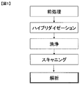
- FIG. 1 shows details of a series of processing steps of DNA chip analysis.
- a DNA sample provided with a fluorescent mark for example, Cy3, Cy5, etc.
- a fluorescent mark for example, Cy3, Cy5, etc.
- the hybridized DNA chip is washed with a predetermined washing solution. As a result, all the DNA samples that have not been combined with the probe DNAs arranged in a grid are washed away.
- the cleaned DNA chip is scanned.
- a DNA chip is irradiated with a laser beam having a predetermined wavelength suitable for exciting a fluorescent mark (for example, Cy3, Cy5, etc.) and scanned in the reader.
- a fluorescent mark for example, Cy3, Cy5, etc.
- the fluorescence intensity of each spot is calculated using the template for the obtained fluorescence image data, and various analyzes are executed.
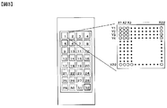
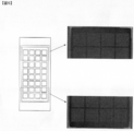
- FIG. 2 shows an example of a DNA chip 1 used for DNA chip analysis.
- a DNA chip 1 shown in FIG. 2 has a block in which a predetermined number of probe DNAs corresponding to individual genes are arranged in a matrix in a row direction and a column direction on a substrate 2 (hereinafter referred to as the block).
- the probe DNA arranged in (3) is called “spot” 3).
- corresponds to the mutually different gene from which the base sequence has already been decoded, respectively,
- substrate 2 is predetermined.
- FIG. 3 shows an example of a template applied to the fluorescence image data of the DNA chip.
- the template is divided into a plurality of blocks such as 1 to 32, and detections arranged in a matrix of m rows and n columns (22 ⁇ 22 in FIG. 3) in each block. Areas (corresponding to individual spots on the DNA chip) are provided.
- the detection area of the template provided by the analysis tool is applied to each spot in the fluorescence image data of the read DNA chip (alignment), and the fluorescence intensity of each spot is calculated in the detection area.
- This alignment method includes a pattern matching method and a projection method for performing alignment in block units. As shown in Patent Document 1, attempts have been made to accurately perform alignment using a fluorescent material called positive control and a chip spotted with a housekeeping gene contained in any specimen. Yes.
- the present invention has been made in order to solve the above-described problems, and is used for analyzing a DNA chip without a positive control or for analyzing a chip with a small amount of DNA contained in a sample.
- An object of the present invention is to provide an analysis method and apparatus capable of appropriately performing processing.
- a microarray analysis method in which excitation light is irradiated onto a microarray in which probes are arranged on a substrate surface having an uneven shape, and the amount of fluorescence from each probe excited by the excitation light is obtained as numerical data.
- a microarray analysis method comprising: (b) obtaining as image data; and (c) determining a position of each probe in the fluorescence image data based on the alignment image data.
- the reflected light and / or scattered light from the substrate surface is light obtained by reflecting and / or scattering light from the light source that irradiates the excitation light on the microarray. analysis method.
- the step (c) includes a step (c1) of detecting three or more reference points A of the microarray based on a difference in received light intensity in the alignment image data, and a step based on the detected reference points A. And (c2) of correcting the distortion of the fluorescence image data, the microarray analysis method according to (1) or (2).
- the step (c1) includes a step (c11) of calculating a contour reference point a that is a point on the contour line of the substrate in each of at least eight predetermined observation regions, and at least two predetermined observation regions that do not overlap.
- the microarray analysis method according to (4) further comprising: (5)
- the step (c2) obtains an array angle ⁇ x, ⁇ y of the spot where the probe is arranged from the reference point A, and calculates the fluorescence image data from the array angle ⁇ x, ⁇ y of the spot and the following formula:
- the step (c1) detects four reference points A, and if the quadrilateral formed by connecting the four reference points A with a straight line is not a parallelogram, the quadrangle is further converted into a parallelogram.
- a laser light source that irradiates excitation light onto a microarray in which a probe is disposed on the surface of a substrate having an uneven shape, an objective lens that collimates the excitation light reflected from the substrate surface and the fluorescent light beam from the probe;
- An optical filter that cuts off the excitation light reflected from the substrate surface and transmits the fluorescence from the probe; an imaging lens that receives the fluorescence transmitted through the optical filter and acquires fluorescence image data; and a detector;
- the image forming lens and the detector receive the light reflected and / or scattered on the substrate surface, and the image data for alignment in which the concavo-convex shape of the substrate surface of the microarray appears.
- a microarray reader comprising an arithmetic processing unit for output.
- the alignment process can be appropriately performed, and the analysis can be performed. .
- FIG. 1 is a schematic diagram of a DNA chip analyzer showing an embodiment of the present invention.
- 1 is a schematic diagram showing an embodiment of an optical system in a DNA chip reader.
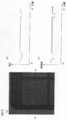
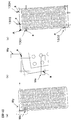
- FIG. 6 is a schematic diagram showing an example of fluorescent image data in which distortion occurs and the spot array does not become vertical despite scanning a DNA chip in which the row direction and the column direction of the spot array are perpendicular to each other. It is an example of the image for alignment obtained with the reading device of the DNA chip.
- the microarray analysis apparatus of the present invention includes a DNA microarray (DNA chip) in which DNA as a probe is immobilized on a substrate, a protein microarray in which a protein as a probe is immobilized on a substrate, and a tissue microarray in which a large number of minute specimens are immobilized on the substrate.
- excitation light is irradiated to a microarray in which probes are arranged on the surface of a substrate having a concavo-convex shape, and the amount of fluorescence from each probe excited by the excitation light is obtained as numerical data.
- Fluorescence image data is acquired by measuring the amount of fluorescence (step (a)), and separately from the step (a), the reflected light and / or scattered light from the substrate surface is received and the received light intensity of the light is received.
- step (b) To obtain the uneven shape on the substrate surface of the microarray as image data for alignment (step (b)). Then, based on the alignment image data obtained in step (b), the position of each probe in the fluorescence image data obtained in step (a) is determined (step (c)).
- the microarray referred to in the present invention is obtained by fixing, for example, tens to tens of thousands of probes on a substrate such as glass or plastic.
- a sample (target) labeled with a fluorescent molecule or the like is applied to the substrate of this microarray, and the binding reaction between the probe and the sample is detected by fluorescence.
- the name is given according to the type of probe to be fixed to the substrate.
- DNA microarray in which DNA is fixed to the substrate
- protein microarray in which protein is fixed to the substrate
- tissue microarrays immobilized on a substrate
- compound microarrays on which a large number of low-molecular compounds are immobilized on a substrate.
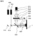
- Analysis of a microarray such as a DNA chip is performed using, for example, a scanner 4, a scanner control PC 5, an image server 6, an analysis PC 7, as shown in FIG.
- the scanner 4 includes a laser light source, an optical filter, an objective optical system, a detector that acquires fluorescence image data and alignment image data, and the like. More specifically, as shown in FIG. 5, for example, the scanner 4 has a scanning mechanism for scanning a substrate such as the DNA chip 1 in two directions (not shown, and in this specification, the longitudinal direction of the chip is defined as the y-axis, A direction orthogonal to the x-axis), an autoloader mechanism (not shown) for mounting a plurality of substrates such as DNA chips, laser light sources 501, 502 for emitting excitation light of a specific wavelength to the substrate surface, While cutting the excitation light from the laser light source 501 and the objective lens 504 that collimates the light (fluorescence) from the probe that has received the excitation light and the reflected / scattered light flux from the substrate surface of the excitation light.
- a scanning mechanism for scanning a substrate such as the DNA chip 1 in two directions (not shown, and in this specification, the longitudinal direction of the chip is defined
- Fluorescence image data is acquired by receiving and imaging fluorescence from the filter 507 and the probe, and reflected and / or scattered light from the substrate surface is received and imaged, and the microarray substrate is obtained from the received light intensity.
- An imaging lens 509 and a detector 511 are provided for acquiring the surface irregularity shape as alignment image data.
- the excitation light is refracted by the mirrors 512 and 513 to reach the DNA chip 1 in order to reduce the size of the apparatus.
- the reference axes of the scanning mechanism are orthogonal to obtain an image without distortion.
- a scanning mechanism it is generally preferable to use a slider for both axes.
- the analysis PC 7 (arithmetic processing unit) is introduced with a program for performing arithmetic processing for detecting the position of each probe in the fluorescence image data based on the alignment image acquired by the detector 511.
- the scanner control PC 5 controls scanning of the DNA chip 1 and image acquisition control by the scanner 4.
- a general-purpose personal computer or the like is used as the scanner control PC 5.
- the obtained fluorescence image data is stored in the image server 6 as a DNA chip image file 8.
- the DNA chip 1 is scanned with an excitation wavelength corresponding to the fluorescent dyes Cy3 and Cy5, for example, and fluorescence image data corresponding to each excitation wavelength is obtained corresponding to one DNA chip 1.
- the fluorescence image data is stored in a file format such as a 16-bit gray scale Tiff format, a BMP format, or a JPEG format.
- the analysis PC 7 reads the DNA chip image file 8 stored in the image server 6. Further, an analysis definition file 9 that defines parameters for executing analysis is read, the analysis of the DNA chip image is executed, and the digitized analysis result data is output as a digitized data file 10.
- the analysis PC 7 is introduced with a program for executing analysis processing including alignment processing described later.
- analysis of a microarray such as a DNA chip is performed by the method as described above.
- the microarray substrate surface is used apart from the step of acquiring fluorescent image data ((step (a) above).
- the reflected light and / or scattered light is received, the uneven shape of the substrate is acquired as alignment image data (step (b) above), alignment processing is performed based on the obtained alignment image data, and fluorescence is obtained.
- the position of each probe in the image data is determined (step (c) above).
- step (a) the image acquisition method corresponding to step (a) will be described with reference to FIG.
- fluorescent dyes include Fluorescin, FITC, Alexa Fluor 555, Rhodamine, Cy3.5, Texas Red, TAMURA, Oyster 650, and Cy5.5.
- laser light that is, excitation light of the fluorescent dye Cy5
- a Cy5 laser light source 501 for example, a laser light source having a wavelength of 635 nm.
- the laser light is applied to the DNA chip 1 through the perforated mirror 503 and the objective lens 504.
- the fluorescent light 505 from the fluorescent molecules excited and emitted by the irradiated laser light and the laser light 506 reflected and / or scattered on the chip surface are collected by the objective lens 504 so as to be substantially parallel to each other. Thereafter, the fluorescence 505 and the laser light 506 are reflected by the perforated mirror 503 and enter the excitation light cut filter 508 for Cy5.
- the laser light regularly reflected on the chip surface passes through the hole of the perforated mirror 503. Fluorescence 505 from the excited fluorescent molecules passes through the excitation light cut filter 508 and is collected by the imaging lens 509. On the other hand, the excitation light (light reflected and / or scattered on the chip surface) reaching the excitation light cut filter 508 is cut.
- the fluorescence 505 collected by the imaging lens 509 is cut by the pinhole 510 except for the light near the focal position of the imaging lens 509 and enters the detector 511.
- the detector 511 outputs an electrical signal corresponding to the intensity of light. Such a process is repeated by scanning the DNA chip 1 in two directions by the scanner control PC 5, and A / D conversion is performed on the electrical signal output from the detector 511 to create fluorescent image data.
- the fluorescent dye Cy3 is read.
- the fluorescent dye Cy3 is read by replacing the Cy5 laser light source 501 with a Cy3 laser light source 502 (for example, a laser light source having a laser wavelength of 532 nm) and replacing the Cy5 excitation light cut filter 508 with the Cy3 excitation light cut filter 507. Except for replacement with the above, the reading may be performed in the same manner as the reading of the fluorescent dye Cy5. That is, the laser light (that is, the excitation light of the fluorescent dye Cy3) is irradiated from the laser light source 502 for Cy3, and the excitation light (that is, the chip surface) that reaches the excitation light cut filter 507 by the excitation light cut filter 507 for Cy3. In this manner, fluorescence image data is created in the same manner as Cy5.
- the scanning mechanism of the scanner is provided with two sliders
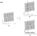
- the sliders are not necessarily orthogonal to each other. It may be shifted when the device is assembled or with the passage of time. Therefore, the image of the DNA chip read by the scanner may also be inclined as shown in FIG. 6A, for example.
- the x-axis and y-axis of the scanning mechanism are not orthogonal, the obtained fluorescence image data is distorted, and the template detection area cannot be correctly aligned with the obtained image.
- the fluorescence image data is projected in the y-axis direction with respect to the x-axis, and the integrated intensity for each coordinate X (the integrated value of each pixel value) is calculated. This process is repeated by rotating the fluorescent image data by a preset angle around the coordinate origin.
- the integrated intensity graph when the projection direction and the arrangement direction of the spot in the y-axis direction are shifted is a graph having no amplitude as shown in FIG.
- the angle of the array with respect to the y-axis of the spot can be detected.
- the array direction of the spots can be made orthogonal by obtaining the array angle with respect to the x-axis and performing image processing such as shear deformation.
- the following alignment image data is also acquired without resetting the chip (step (b) above). That is, the image data for alignment is obtained by irradiating the DNA chip 1 with light and receiving reflected light and / or scattered light from the substrate surface of the chip. This is because it actively receives reflected light and / or scattered light from the substrate surface having a concavo-convex shape, images the concavo-convex shape on the substrate surface based on the received light intensity of the light, and uses the concavo-convex shape for alignment. It is.
- the spot position on the DNA chip does not change until the DNA chip is reset. Therefore, the spot position in the alignment image data and the spot arrangement in the fluorescence image data of Cy5 and Cy3 coincide. Therefore, in the present invention, the alignment result of the image data for alignment is applied to the fluorescence image data of Cy5 and Cy3, thereby enabling alignment processing of the fluorescence image data.
- the excitation light cut filter 507 is light having a wavelength of excitation light of Cy5 (635 nm).
- the OD value of light of 635 nm is about 5
- FIG. 7B shows the profile of the pixel value in the P-P ′ line segment of FIG. 7A
- FIG. 7C shows the height profile of the DNA chip at the corresponding location.
- a light source for acquiring alignment image data it is preferable to use a light source that emits excitation light for exciting fluorescent molecules because the number of parts of the scanner can be reduced.
- a separate light source for acquiring alignment image data is provided. It doesn't matter.
- a method that does not use a filter when acquiring alignment image data can be adopted.
- the filter when the filter is not used, the amount of light entering the detector becomes too large, and the detector may be damaged. Therefore, as described above, when irradiating laser light from the Cy5 laser light source 501, it is preferable to use a filter that slightly transmits the wavelength of the irradiating light source, such as using the excitation light cut filter 507.
- the excitation light cut filter 508 may be used by irradiating laser light from the laser light source 502 for Cy3.
- an ND filter is used in place of the excitation light cut filters 507 and 508, or the laser light output itself is weakened without using the excitation light cut filters 507 and 508 and the ND filter to obtain alignment image data. It doesn't matter. Of course, combinations of these can also be applied.
- the spot position in the alignment image data matches the spot arrangement in the fluorescence image data of Cy5 and Cy3.
- Step (c) the position of each probe in the fluorescence image data is determined based on the alignment image data (step (c) above), and the microarray is analyzed. Details of this method will be described below with reference to the block diagram shown in FIG. However, Steps 1 and 2 in FIG. 8 are steps corresponding to the steps described above.
- Step 1 the DNA chip is set in the scanner, and the fluorescent image data of the fluorescent dyes Cy5 and Cy3 are read as described above (step (a) above).
- Step 2 while the DNA chip is set, the excitation light is irradiated from the Cy5 laser light source 501 and the alignment image is read using the Cy3 excitation light cut filter 507 (step (b) above). ).
- excitation light may be emitted from the Cy3 laser light source 502 and the excitation light cut filter 508 for Cy5 may be used.
- another light source may be prepared, and reflected light and / or scattered light from the DNA chip may be received to obtain an alignment image.
- Step 3 the position of each probe in the fluorescence image data is determined using the alignment image data (step (c) above) and analyzed.
- At Step 3 at least three reference points A in the alignment image data are detected (step (c1)).
- at least three reference points A for example, as shown in FIG. 9, the coordinates of the four corners in the alignment image can be mentioned.
- edge detection using light / dark information, pattern matching using the four corner images as a master image, and the like using the light / dark information are also desirable.
- Steps 4 and 5 the distortion of the fluorescence image data is corrected based on the reference point A (step (c2)).
- Step 4 for example, from the coordinates of the above-mentioned four corners, the array angle with respect to the x-axis of the spot (the inclination angle with respect to the x-axis of the line that linearly connects the nearest adjacent spots) ⁇ x, the y-axis of the spot An array angle with respect to (a tilt angle with respect to the y-axis of a line connecting the nearest adjacent spots linearly) ⁇ y is detected. It is desirable that ⁇ x and ⁇ y take an average value of the angles of the two line segments in the corresponding direction for the four line segments connecting the coordinates of the four corners. Note that even if there are three reference points, ⁇ x and ⁇ y can be calculated. Then, as shown in FIGS. 10A and 10B, the fluorescence image data is rotated using the array angle ⁇ y of the spots with respect to the y-axis as a correction angle, so that the spots are parallel to the y-axis.
- Step 5 conversion (shear deformation) is performed on the rotated image based on the arrangement angles ⁇ x and ⁇ y of the spots regularly arranged in the two directions detected as described above and the following expression. To do. Thereby, the shear deformation distortion of the image is corrected.
- the image after this conversion is shown in FIG.
- (x, y) are coordinates before conversion
- (X, Y) are coordinates after conversion.
- ⁇ xy corresponding to the deviation of the scanning mechanism of the scanner is obtained by subtracting the array angle ⁇ y with respect to the y axis from the array angle ⁇ x with respect to the x axis of the spot, as shown in Equation 4. .
- the resin may expand due to moisture absorption or temperature change in the hybridization process or the washing process. Although it depends on the processing time in each process, it may expand several tens of ⁇ m, which affects the alignment accuracy.
- Steps 6 and 7 for example, the chip lengths in the x-axis direction and the y-axis direction are calculated from the coordinates of the four corners, and the fluorescence image data is contracted so as to coincide with the design values.
- each spot in the template stored in the analysis definition file in advance is, for example, the center coordinates of each spot with the upper left corner of the chip as the origin.
- each spot frame is calculated using the coordinates of the upper left corner as the origin, and alignment can be performed as shown in FIGS. 11B and 11C (Step 8).
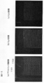
- FIG. 11B is an image showing the result of alignment with Cy3 fluorescence image data
- FIG. 11C is an image showing the result of alignment with Cy5 fluorescence image data.
- the result of alignment performed on the image data for alignment obtained in Step 2 is shown in FIG.
- the inside of a circle drawn with a dotted line is a detection area defined by the template.
- Step 9 statistics such as average value, median value, standard deviation, etc. are calculated for the signal intensity of the pixels within the spot radius from the center coordinates of each spot obtained in Step 8, and the block number to which the spot belongs, the spot number Together with the matrix number and the name of the arranged probe DNA, various numerical data are output as a file.
- Steps 1 and 2 may be changed.
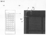
- a contour point detection window (observation area) Wy including a contour line substantially continuing in the x-axis direction in the vicinity of each of the four corners of the DNA chip, and a substantial y-axis direction.
- a contour point detection window Wx that includes a contour line following is set. Then, in each of the contour point detection windows Wx and Wy, the contour reference point a corresponding to one point on the contour line of the DNA chip is detected, the y coordinate of the contour reference point a in the window Wy, and the contour reference point in the window Wx From the x coordinate of a, the coordinate of the reference point A corresponding to the corner of the DNA chip is calculated. This is done for example at the four corners.
- At least four contour point detection windows Wx and Wy that is, a total of eight or more.
- at least two contour point detection windows Wx (1301, 1302) and at least two contour point detection windows Wy (1303, 1304) are provided for each of the four corners. Is preferably set (step (c11)).
- the at least two contour point detection windows Wx (1301, 1302) are paired, an approximate straight line for the plurality of contour reference points a in the pair is obtained, and at least two contour point detection points are detected.
- the window Wy (1303, 1304) as a set, an approximate straight line for a plurality of contour reference points a in the set is obtained (step (c12)).
- the intersection of the two approximate lines obtained in this way is obtained, and the intersection is set as a reference point A (step (c13)).
- the reference points A may be calculated at the three corners.
- the reference point A when the reference point A is detected as described above, a measurement error occurs if there is a scratch or dust in the detection unit. Therefore, even if four reference points A corresponding to the four corners of the substrate are detected, the shape formed by connecting these four reference points A is not a parallelogram (including a rectangle and a square), such as a trapezoid. It may be a rectangle.
- the correction of the shear deformation distortion in the subsequent processing Step 5 is based on the premise that the shape formed by the detected reference points is a parallelogram, and therefore, in the above case, the spots may not be well aligned. There is.
- fluorescent image data obtained based on gene expression in this way is processed to obtain desired numerical data.
- the various numerical data obtained are the presence of the desired gene in the specimen. It is also used to analyze whether or how much a certain gene is expressed.
- the present invention can also be applied to a chip spotted with RNA, protein, minute sample, low molecular weight compound, cell, etc. It is.
- the same method is used even when a protein (antibody) is immobilized on a substrate of a DNA chip having an uneven shape as described above, instead of DNA, and the presence / absence of a reaction with a sample or quantification is detected by fluorescence. be able to.
- the protein present in the sample cell lysate is labeled with Cy5 and the protein present in the control cell lysate is labeled with Cy3 and both are mixed and reacted with the antibody array, or the protein is labeled with biotin instead of fluorescently labeling.
- biotin instead of fluorescently labeling.
- RNA array this method can be used when detecting hybridization of RNA immobilized on a substrate having an uneven shape and fluorescently labeled DNA or RNA by fluorescence.
- the present invention can be applied when detecting a binding reaction between a micro sample or a cell immobilized on a substrate having an uneven shape and a fluorescent labeled specimen (for example, an antibody) by fluorescence. Is possible.
Landscapes
- Health & Medical Sciences (AREA)
- Life Sciences & Earth Sciences (AREA)
- Engineering & Computer Science (AREA)
- Immunology (AREA)
- Chemical & Material Sciences (AREA)
- Physics & Mathematics (AREA)
- Molecular Biology (AREA)
- General Health & Medical Sciences (AREA)
- Biomedical Technology (AREA)
- Biochemistry (AREA)
- Analytical Chemistry (AREA)
- Biotechnology (AREA)
- Pathology (AREA)
- General Physics & Mathematics (AREA)
- Urology & Nephrology (AREA)
- Hematology (AREA)
- Bioinformatics & Cheminformatics (AREA)
- Microbiology (AREA)
- Medicinal Chemistry (AREA)
- Food Science & Technology (AREA)
- Cell Biology (AREA)
- Genetics & Genomics (AREA)
- Nuclear Medicine, Radiotherapy & Molecular Imaging (AREA)
- Evolutionary Biology (AREA)
- Biophysics (AREA)
- Bioinformatics & Computational Biology (AREA)
- Medical Informatics (AREA)
- Spectroscopy & Molecular Physics (AREA)
- Theoretical Computer Science (AREA)
- Wood Science & Technology (AREA)
- Zoology (AREA)
- Organic Chemistry (AREA)
- Sustainable Development (AREA)
- General Engineering & Computer Science (AREA)
- Investigating, Analyzing Materials By Fluorescence Or Luminescence (AREA)
- Apparatus Associated With Microorganisms And Enzymes (AREA)
Priority Applications (7)
| Application Number | Priority Date | Filing Date | Title |
|---|---|---|---|
| KR1020137019910A KR101885939B1 (ko) | 2011-01-28 | 2011-12-26 | 마이크로어레이의 해석 방법 및 판독 장치 |
| RU2013139860/28A RU2013139860A (ru) | 2011-01-28 | 2011-12-26 | Способ анализа микрочипа и устройство считывания микрочипа |
| CA2825727A CA2825727C (en) | 2011-01-28 | 2011-12-26 | Microarray analysis method and microarray reading device |
| BR112013019162A BR112013019162A2 (pt) | 2011-01-28 | 2011-12-26 | método de análise e dispositivo de leitura de microarranjo |
| EP11857286.6A EP2669662B1 (en) | 2011-01-28 | 2011-12-26 | Analysis method and reading device for microarray |
| CN201180066561.6A CN103339493B (zh) | 2011-01-28 | 2011-12-26 | 微阵列的分析方法及读取装置 |
| US13/981,787 US9719929B2 (en) | 2011-01-28 | 2011-12-26 | Microarray analysis method and microarray reading device |
Applications Claiming Priority (4)
| Application Number | Priority Date | Filing Date | Title |
|---|---|---|---|
| JP2011016690 | 2011-01-28 | ||
| JP2011-016690 | 2011-01-28 | ||
| JP2011-205865 | 2011-09-21 | ||
| JP2011205865A JP5817378B2 (ja) | 2011-01-28 | 2011-09-21 | マイクロアレイの解析方法および読取り装置 |
Publications (1)
| Publication Number | Publication Date |
|---|---|
| WO2012101943A1 true WO2012101943A1 (ja) | 2012-08-02 |
Family
ID=46580525
Family Applications (1)
| Application Number | Title | Priority Date | Filing Date |
|---|---|---|---|
| PCT/JP2011/080007 WO2012101943A1 (ja) | 2011-01-28 | 2011-12-26 | マイクロアレイの解析方法および読取り装置 |
Country Status (9)
Cited By (2)
| Publication number | Priority date | Publication date | Assignee | Title |
|---|---|---|---|---|
| WO2014057893A1 (ja) * | 2012-10-12 | 2014-04-17 | 東レ株式会社 | 検出方法、マイクロアレイの解析方法および蛍光読取装置 |
| WO2014198520A1 (de) * | 2013-06-14 | 2014-12-18 | Robert Bosch Gmbh | Erfassungssystem zum erfassen einer lötverbindung |
Families Citing this family (14)
| Publication number | Priority date | Publication date | Assignee | Title |
|---|---|---|---|---|
| KR101594523B1 (ko) * | 2013-09-02 | 2016-02-16 | 한국광기술원 | 가시광 광학영상 및 비가시광 형광영상의 동시구현이 가능한 광대역 영상 획득투사장치 |
| JP2015194379A (ja) * | 2014-03-31 | 2015-11-05 | 株式会社ニコン | バイオチップ及びバイオチップにおけるアライメントマークの検出方法 |
| JP6448933B2 (ja) * | 2014-07-09 | 2019-01-09 | 日本板硝子株式会社 | 蛍光検出用光学装置 |
| JP6534318B2 (ja) * | 2015-09-02 | 2019-06-26 | アズビル株式会社 | 蛍光粒子の計測方法 |
| NL2018852B1 (en) | 2017-05-05 | 2018-11-14 | Illumina Inc | Optical distortion correction for imaged samples |
| JP2018124289A (ja) * | 2018-04-10 | 2018-08-09 | 株式会社ニコン | バイオチップ及びバイオチップにおけるアライメントマークの検出方法 |
| CN109003910B (zh) * | 2018-06-06 | 2020-07-14 | 广东利扬芯片测试股份有限公司 | 基于全自动探针台的不规则晶圆测试方法及其计算机可读存储介质 |
| JP7141102B2 (ja) * | 2018-11-26 | 2022-09-22 | 株式会社マルコム | Led装置の発光特性測定装置 |
| JP6664462B2 (ja) * | 2018-12-05 | 2020-03-13 | 日本板硝子株式会社 | 蛍光検出用光学装置 |
| GB2594813A (en) * | 2019-01-09 | 2021-11-10 | Hitachi High Tech Corp | Substrate for nucleic acid analysis, flow cell for nucleic acid analysis, and image analysis method |
| JP2020106535A (ja) * | 2020-02-18 | 2020-07-09 | 日本板硝子株式会社 | 蛍光検出用光学装置 |
| US20240183795A1 (en) * | 2021-06-18 | 2024-06-06 | Hamamatsu Photonics K.K. | Measuring device |
| WO2022264521A1 (ja) * | 2021-06-18 | 2022-12-22 | 浜松ホトニクス株式会社 | 測定装置 |
| CN117351077B (zh) * | 2023-09-14 | 2024-07-02 | 广东凯普科技智造有限公司 | 一种点样仪动态预测的视觉修正方法 |
Citations (7)
| Publication number | Priority date | Publication date | Assignee | Title |
|---|---|---|---|---|
| JP2003156442A (ja) * | 2001-11-22 | 2003-05-30 | Inst Of Physical & Chemical Res | 生体分子マイクロアレイのデータ収集方法 |
| JP2003307518A (ja) * | 2002-02-14 | 2003-10-31 | Ngk Insulators Ltd | プローブ反応性チップ、試料解析装置および試料解析方法 |
| JP2005024532A (ja) * | 2003-06-13 | 2005-01-27 | Institute Of Physical & Chemical Research | 生体分子マイクロアレイ用基板、生体分子マイクロアレイ、相互作用促進用装置および方法、ならびに、相互作用の検出方法 |
| JP2005049282A (ja) * | 2003-07-30 | 2005-02-24 | Hamamatsu Photonics Kk | 蛍光観察装置及びレーザ光照射装置 |
| JP2005172840A (ja) | 2002-02-14 | 2005-06-30 | Ngk Insulators Ltd | 試料解析装置および試料解析方法 |
| JP2010526314A (ja) * | 2007-05-07 | 2010-07-29 | ベアマン | 試験システム及び試験される電気部材を揃える方法及び装置 |
| WO2010147167A1 (ja) * | 2009-06-16 | 2010-12-23 | 東洋鋼鈑株式会社 | マイクロアレイにおけるプローブ位置決定の方法 |
Family Cites Families (11)
| Publication number | Priority date | Publication date | Assignee | Title |
|---|---|---|---|---|
| US6309601B1 (en) * | 1993-11-01 | 2001-10-30 | Nanogen, Inc. | Scanning optical detection system |
| WO2003044527A1 (fr) | 2001-11-22 | 2003-05-30 | Riken | Substrat pour microreseau de biomolecules, son processus de fabrication, microreseau de biomolecules et procede de collecte de donnees sur microreseau de biomolecules |
| US7200254B2 (en) | 2002-02-14 | 2007-04-03 | Ngk Insulators, Ltd. | Probe reactive chip, sample analysis apparatus, and method thereof |
| US20030152255A1 (en) | 2002-02-14 | 2003-08-14 | Ngk Insulators, Ltd. | Probe reactive chip, apparatus for analyzing sample and method thereof |
| EP1345026B1 (en) * | 2002-03-15 | 2010-05-05 | Affymetrix, Inc. | System and method for scanning of biological materials |
| WO2008104922A1 (en) * | 2007-03-01 | 2008-09-04 | Koninklijke Philips Electronics N.V. | Grid pattern determination system |
| JP2009068995A (ja) * | 2007-09-13 | 2009-04-02 | Panasonic Corp | マイクロアレイ装置 |
| US20100204057A1 (en) * | 2009-02-10 | 2010-08-12 | Samsung Electronics Co., Ltd. | Substrate for microarray, method of manufacturing microarray using the same and method of obtaining light data from microarray |
| KR101513602B1 (ko) * | 2009-02-11 | 2015-04-22 | 삼성전자주식회사 | 바이오칩 스캐닝 방법 |
| JP5409237B2 (ja) * | 2009-09-28 | 2014-02-05 | キヤノン株式会社 | パターン検出装置、その処理方法及びプログラム |
| JP2011182705A (ja) * | 2010-03-09 | 2011-09-22 | Toray Ind Inc | Dnaチップ解析方法および解析装置 |
-
2011
- 2011-09-21 JP JP2011205865A patent/JP5817378B2/ja active Active
- 2011-12-26 CA CA2825727A patent/CA2825727C/en active Active
- 2011-12-26 EP EP11857286.6A patent/EP2669662B1/en active Active
- 2011-12-26 WO PCT/JP2011/080007 patent/WO2012101943A1/ja active Application Filing
- 2011-12-26 RU RU2013139860/28A patent/RU2013139860A/ru not_active Application Discontinuation
- 2011-12-26 US US13/981,787 patent/US9719929B2/en active Active
- 2011-12-26 BR BR112013019162A patent/BR112013019162A2/pt not_active IP Right Cessation
- 2011-12-26 KR KR1020137019910A patent/KR101885939B1/ko active Active
- 2011-12-26 CN CN201180066561.6A patent/CN103339493B/zh active Active
Patent Citations (7)
| Publication number | Priority date | Publication date | Assignee | Title |
|---|---|---|---|---|
| JP2003156442A (ja) * | 2001-11-22 | 2003-05-30 | Inst Of Physical & Chemical Res | 生体分子マイクロアレイのデータ収集方法 |
| JP2003307518A (ja) * | 2002-02-14 | 2003-10-31 | Ngk Insulators Ltd | プローブ反応性チップ、試料解析装置および試料解析方法 |
| JP2005172840A (ja) | 2002-02-14 | 2005-06-30 | Ngk Insulators Ltd | 試料解析装置および試料解析方法 |
| JP2005024532A (ja) * | 2003-06-13 | 2005-01-27 | Institute Of Physical & Chemical Research | 生体分子マイクロアレイ用基板、生体分子マイクロアレイ、相互作用促進用装置および方法、ならびに、相互作用の検出方法 |
| JP2005049282A (ja) * | 2003-07-30 | 2005-02-24 | Hamamatsu Photonics Kk | 蛍光観察装置及びレーザ光照射装置 |
| JP2010526314A (ja) * | 2007-05-07 | 2010-07-29 | ベアマン | 試験システム及び試験される電気部材を揃える方法及び装置 |
| WO2010147167A1 (ja) * | 2009-06-16 | 2010-12-23 | 東洋鋼鈑株式会社 | マイクロアレイにおけるプローブ位置決定の方法 |
Non-Patent Citations (1)
| Title |
|---|
| See also references of EP2669662A4 |
Cited By (9)
| Publication number | Priority date | Publication date | Assignee | Title |
|---|---|---|---|---|
| WO2014057893A1 (ja) * | 2012-10-12 | 2014-04-17 | 東レ株式会社 | 検出方法、マイクロアレイの解析方法および蛍光読取装置 |
| KR20150064067A (ko) * | 2012-10-12 | 2015-06-10 | 도레이 카부시키가이샤 | 검출 방법, 마이크로어레이의 해석 방법 및 형광 판독 장치 |
| CN104718427A (zh) * | 2012-10-12 | 2015-06-17 | 东丽株式会社 | 检测方法、微阵列的分析方法及荧光读取装置 |
| EP2908089A4 (en) * | 2012-10-12 | 2016-06-08 | Toray Industries | DETECTION METHOD, MICROARRAY ANALYSIS PROCEDURE AND FLUORESCENT READING |
| JPWO2014057893A1 (ja) * | 2012-10-12 | 2016-09-05 | 東レ株式会社 | 検出方法、マイクロアレイの解析方法および蛍光読取装置 |
| US9823197B2 (en) | 2012-10-12 | 2017-11-21 | Toray Industries, Inc. | Detecting method, microarray analyzing method, and fluorescence reading device |
| KR102136648B1 (ko) * | 2012-10-12 | 2020-07-22 | 도레이 카부시키가이샤 | 검출 방법, 마이크로어레이의 해석 방법 및 형광 판독 장치 |
| WO2014198520A1 (de) * | 2013-06-14 | 2014-12-18 | Robert Bosch Gmbh | Erfassungssystem zum erfassen einer lötverbindung |
| US9645098B2 (en) | 2013-06-14 | 2017-05-09 | Robert Bosch Gmbh | Detection system for detecting a soldered joint |
Also Published As
| Publication number | Publication date |
|---|---|
| US9719929B2 (en) | 2017-08-01 |
| CN103339493A (zh) | 2013-10-02 |
| JP2012168159A (ja) | 2012-09-06 |
| JP5817378B2 (ja) | 2015-11-18 |
| EP2669662A4 (en) | 2017-12-27 |
| KR101885939B1 (ko) | 2018-08-06 |
| BR112013019162A2 (pt) | 2018-06-05 |
| EP2669662B1 (en) | 2019-02-20 |
| CA2825727A1 (en) | 2012-08-02 |
| CN103339493B (zh) | 2015-06-10 |
| US20130303403A1 (en) | 2013-11-14 |
| CA2825727C (en) | 2019-03-19 |
| KR20130142179A (ko) | 2013-12-27 |
| EP2669662A1 (en) | 2013-12-04 |
| RU2013139860A (ru) | 2015-03-10 |
Similar Documents
| Publication | Publication Date | Title |
|---|---|---|
| JP5817378B2 (ja) | マイクロアレイの解析方法および読取り装置 | |
| JP6291842B2 (ja) | 検出方法、マイクロアレイの解析方法および蛍光読取装置 | |
| US20120126142A1 (en) | Fluorescent analysis method | |
| JP2017504307A (ja) | アレイ上のフィーチャーをデジタルカウントするための方法およびシステム | |
| JP2011182705A (ja) | Dnaチップ解析方法および解析装置 | |
| US20220412872A1 (en) | Linear fourier fiducial | |
| JP2024534332A (ja) | 周期的にパターン化された表面のためのシーケンサ焦点品質メトリック及び焦点追跡 | |
| KR102048599B1 (ko) | 판정 방법, 판정 장치, 판정 시스템 및 프로그램 | |
| JP2013224894A (ja) | マイクロアレイの解析方法 | |
| US20110081098A1 (en) | Method of correcting distortion of scanned image | |
| JP2004184379A (ja) | マイクロアレイの読取方法 | |
| CA3224034A1 (en) | Linear fourier fiducial | |
| US20240100518A1 (en) | Flow cell based motion system calibration and control methods | |
| US20220414853A1 (en) | Fiducials for use in registration of a patterned surface | |
| KR101188233B1 (ko) | 바이오칩을 위한 진단장치 | |
| CN117859086A (zh) | 用于周期性图案化表面的测序仪聚焦质量度量和聚焦跟踪 | |
| JP2012189337A (ja) | 蛍光検出装置 |
Legal Events
| Date | Code | Title | Description |
|---|---|---|---|
| 121 | Ep: the epo has been informed by wipo that ep was designated in this application |
Ref document number: 11857286 Country of ref document: EP Kind code of ref document: A1 |
|
| ENP | Entry into the national phase |
Ref document number: 2825727 Country of ref document: CA |
|
| WWE | Wipo information: entry into national phase |
Ref document number: 13981787 Country of ref document: US |
|
| ENP | Entry into the national phase |
Ref document number: 20137019910 Country of ref document: KR Kind code of ref document: A |
|
| WWE | Wipo information: entry into national phase |
Ref document number: 2011857286 Country of ref document: EP |
|
| NENP | Non-entry into the national phase |
Ref country code: DE |
|
| ENP | Entry into the national phase |
Ref document number: 2013139860 Country of ref document: RU Kind code of ref document: A |
|
| REG | Reference to national code |
Ref country code: BR Ref legal event code: B01A Ref document number: 112013019162 Country of ref document: BR |
|
| REG | Reference to national code |
Ref country code: BR Ref legal event code: B01E Ref document number: 112013019162 Country of ref document: BR Free format text: APRESENTE A TRADUCAO SIMPLES DA FOLHA DE ROSTO DA CERTIDAO DE DEPOSITO DAS PRIORIDADES JP2011-016690 E JP2011-205865; OU DECLARACAO DE QUE OS DADOS DO PEDIDO INTERNACIONAL ESTAO FIELMENTE CONTIDOS NA PRIORIDADE REIVINDICADA, CONTENDO TODOS OS DADOS IDENTIFICADORES DESTAS (TITULARES, NUMERO DE REGISTRO, DATA E TITULO), CONFORME O PARAGRAFO UNICO DO ART. 25 DA RESOLUCAO 77/2013. Ref country code: BR Ref legal event code: B01E Ref document number: 112013019162 Country of ref document: BR |
|
| ENP | Entry into the national phase |
Ref document number: 112013019162 Country of ref document: BR Kind code of ref document: A2 Effective date: 20130726 |