WO2012086596A1 - カバーガラス一体型センサー - Google Patents
カバーガラス一体型センサー Download PDFInfo
- Publication number
- WO2012086596A1 WO2012086596A1 PCT/JP2011/079382 JP2011079382W WO2012086596A1 WO 2012086596 A1 WO2012086596 A1 WO 2012086596A1 JP 2011079382 W JP2011079382 W JP 2011079382W WO 2012086596 A1 WO2012086596 A1 WO 2012086596A1
- Authority
- WO
- WIPO (PCT)
- Prior art keywords
- frame
- shaped light
- shielding layer
- cover glass
- film
- Prior art date
- Legal status (The legal status is an assumption and is not a legal conclusion. Google has not performed a legal analysis and makes no representation as to the accuracy of the status listed.)
- Ceased
Links
Images











Classifications
-
- G—PHYSICS
- G06—COMPUTING OR CALCULATING; COUNTING
- G06F—ELECTRIC DIGITAL DATA PROCESSING
- G06F3/00—Input arrangements for transferring data to be processed into a form capable of being handled by the computer; Output arrangements for transferring data from processing unit to output unit, e.g. interface arrangements
- G06F3/01—Input arrangements or combined input and output arrangements for interaction between user and computer
- G06F3/03—Arrangements for converting the position or the displacement of a member into a coded form
- G06F3/041—Digitisers, e.g. for touch screens or touch pads, characterised by the transducing means
- G06F3/044—Digitisers, e.g. for touch screens or touch pads, characterised by the transducing means by capacitive means
- G06F3/0446—Digitisers, e.g. for touch screens or touch pads, characterised by the transducing means by capacitive means using a grid-like structure of electrodes in at least two directions, e.g. using row and column electrodes
-
- H—ELECTRICITY
- H01—ELECTRIC ELEMENTS
- H01H—ELECTRIC SWITCHES; RELAYS; SELECTORS; EMERGENCY PROTECTIVE DEVICES
- H01H9/00—Details of switching devices, not covered by groups H01H1/00 - H01H7/00
- H01H9/02—Bases, casings, or covers
-
- H—ELECTRICITY
- H03—ELECTRONIC CIRCUITRY
- H03K—PULSE TECHNIQUE
- H03K17/00—Electronic switching or gating, i.e. not by contact-making and –breaking
- H03K17/94—Electronic switching or gating, i.e. not by contact-making and –breaking characterised by the way in which the control signals are generated
- H03K17/96—Touch switches
- H03K17/962—Capacitive touch switches
Definitions
- the present invention relates to a cover glass integrated sensor in which a capacitive film sensor is bonded to the back surface of a cover glass attached to a liquid crystal display unit of an electronic device.
- a cover glass is attached to a liquid crystal display window of an electronic device or the like to protect it.
- this cover glass has a black frame-shaped light shielding layer formed on the peripheral edge of the back surface of a transparent glass substrate.
- touch panels are often used in the electronic devices described above, and the recent trend is to enlarge or reduce the image by tapping, flipping, and picking the screen with the fingertips compared to the current mainstream resistive film method. Due to its excellent multi-touch function, visibility, and durability, there is a great need for a capacitive method.
- a capacitive film sensor 103 as disclosed in Patent Document 1 is used and bonded to the back surface of the cover glass 102. The market for the bar glass integrated sensor 101 (see FIG. 6) is expected to expand.
- the frame-shaped light-shielding layer 105 of the cover glass 102 is formed by screen printing using a light-shielding ink such as black on the periphery of the back surface of the transparent glass substrate 104, the frame-shaped light shielding layer formed by this method is used.
- Layer 105 has very poor inner edge linearity. Therefore, there is a problem that the outline of the display screen viewed through the cover glass 102 looks blurred (see FIG. 7).
- the frame-shaped light shielding layer of the cover glass formed by screen printing has to be overprinted by about three layers of the printed film in order to obtain light shielding properties. A big step is generated between them. Because of this step, bubbles (bubbles) are likely to be generated when the film sensor is attached to the back of the cover glass with a transparent adhesive, and the generated bubbles can be moved to the outside by pressing to slide. It is difficult to remove, resulting in poor visibility of the display screen.
- the inner edge of the black mask surrounding the display screen in the display device is positioned closer to the center side than the inner edge of the frame-shaped light shielding layer of the cover glass. Is located behind the polarizing plate and the upper glass substrate, and there is a large depth difference between the exposed part of the black mask and the frame-shaped light shielding layer of the cover glass, so that the part surrounding the display screen has no sense of unity in appearance. Another problem arises.
- an object of the present invention is to solve the above-mentioned problems, and the display screen viewed through the cover glass has a sharp outline, excellent visibility, and a cover having an appearance and a sense of unity around the display screen.
- the object is to provide a glass integrated sensor.
- a cover glass for an electronic device display window in which a first frame-shaped light-shielding layer made of a screen printing film is formed on the peripheral edge of the back surface of a transparent glass substrate;
- a cover glass integrated sensor comprising a capacitive film sensor bonded to the back surface of the cover glass,
- the film sensor is A transparent substrate sheet;
- a transparent conductive film formed on both surfaces of the base sheet so as to have an electrode pattern of a central window part and a thin line drawing circuit pattern of an outer frame part, and the thin line on the thin line drawing circuit pattern of the transparent conductive film, respectively.
- the film sensor has a second frame-shaped light-shielding layer made of an exposure developer of a color resist material, formed on the peripheral edge of the surface of the base sheet, and an inner edge of the second frame-shaped light-shielding layer Is located closer to the center than the inner edge of the first frame-shaped light shielding layer, A cover glass integrated sensor is provided.
- the second frame-shaped light-shielding layer may be formed as a separate layer in addition to the transparent conductive film, the light-shielding conductive film, and the rust-preventing functional layer. It may also serve as a rust functional layer.
- the former was formed on the surface peripheral portion of the base sheet formed on the surface peripheral portion of the base sheet on which the transparent conductive film, the light-shielding conductive film and the rust prevention functional layer were formed.
- the second frame-shaped light-shielding layer made of an exposure developer of a color resist material is formed, and the latter is a second frame-shaped light-shielding layer in which the anticorrosive function layer is made of an exposure developer of a color resist material. It has worked.
- the cover glass integrated sensor according to the first aspect, wherein the distance between the back surface of the glass substrate and the second frame-shaped light shielding layer is 10 ⁇ m to 100 ⁇ m.
- the color in the vicinity of the inner edge of the first frame-shaped light-shielding layer and the color of the second frame-shaped light-shielding layer are the same color or similar colors.
- An embodiment of the integrated cover glass sensor is provided.
- the cover glass integrated sensor according to the first to fourth aspects, wherein the color of the second frame-shaped light shielding layer is black or white.
- the first frame-shaped light shielding layer has a thickness of 7 ⁇ m to 30 ⁇ m
- the second frame-shaped light shielding layer has a thickness of 2 ⁇ m to 25 ⁇ m.
- the difference between the inner edge dimension of the second frame-shaped light shielding layer and the inner edge dimension of the first frame-shaped light shielding layer is 0.1 mm to 0.3 mm.
- a cover glass integrated sensor according to any one of the first to sixth aspects is provided.
- the cover glass integrated sensor of the present invention is formed so that the film sensor has a transparent base sheet and an electrode pattern of the central window part and a thin line drawing circuit pattern of the outer frame part on both sides of the base sheet.
- a light shielding conductive film laminated with the same width as the thin conductive circuit pattern, the transparent conductive film, and the light shielding conductive film were formed.
- a rust preventive functional layer laminated on both sides of the base sheet so as to cover the outer frame part other than the terminal part, and the film sensor is provided on the peripheral edge of the surface of the base sheet.
- a second frame-shaped light-shielding layer made of an exposure developer of a color resist material is formed, and the inner edge of the second frame-shaped light-shielding layer is a frame-shaped light shielding layer of a cover glass It is located at the center side of the inner edge of the first frame-shaped light shielding layer). Therefore, since the second frame-shaped light-shielding layer has very good linearity at the inner edge made of the color resist material exposed developer, the outline of the display screen seen through the cover glass looks sharp.
- the film sensor since the film sensor includes the second frame-shaped light-shielding layer, light is shielded by a laminated structure of the second frame-shaped light-shielding layer and the first frame-shaped light shielding layer of the cover glass formed by screen printing. Sex can be obtained. That is, the first frame-shaped light-shielding layer may be thinner than the conventional one, and the level difference between the back surface peripheral edge portion and the back surface center portion of the glass substrate can be suppressed small. Therefore, when the film sensor is bonded to the back surface of the cover glass with a transparent adhesive, bubbles (bubbles) are not easily generated, and even if they are generated, they are moved to the outside by pressing to slide the bubbles and removed. As a result, the visibility of the display screen is excellent.
- the film sensor since the film sensor includes the second frame-shaped light shielding layer, there is almost no difference in depth between the exposed portion of the second frame-shaped light shielding layer and the first frame-shaped light shielding layer of the cover glass. A sense of unity in appearance can be obtained at the part surrounding the screen.
- FIG. 1 is an exploded cross-sectional view showing an embodiment of the cover glass integrated sensor according to the present invention
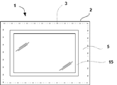
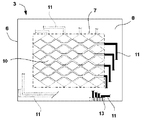
- FIG. 2 is a plan view showing an embodiment of the cover glass integrated sensor according to the present invention.
- 1 is a cover glass integrated sensor
- 2 is a cover glass
- 3 is a film sensor 4 is a glass substrate
- 5 is a first frame-shaped light shielding layer
- 6 is a base sheet
- 7 is a central window portion
- 8 is an outer frame.
- Part 9 is a transparent conductive film
- 10 is an electrode pattern
- 11 is a thin line drawing circuit pattern
- 12 is a light-shielding conductive film
- 13 is a terminal part
- 14 is a rust prevention functional layer
- 15 is a second frame-shaped light shielding layer. Show.
- the cover glass integrated sensor 1 of the present invention is an electronic device display window in which a first frame-shaped light-shielding layer 5 made of a screen printing film is formed on the back peripheral edge of a transparent glass substrate 4.
- the cover glass integrated sensor includes a cover glass 2 and a capacitive film sensor 3 bonded to the back surface of the cover glass 2.
- the cover glass 2 of the electronic device display window is arranged on a display device of an electronic device (not shown) to protect it.
- the glass substrate 4 of the cover glass for example, a transparent glass plate made of colorless and transparent soda lime silicate glass, aluminosilicate glass, lithium aluminosilicate glass, quartz glass, alkali-free glass, and other various glasses can be used. .
- the thickness of the glass substrate 4 is preferably 0.3 to 0.7 mm, and more preferably 0.4 to 0.55 mm. When the thickness of the glass substrate 4 is within this range, it is preferable because the obtained cover glass 2 of the present invention has an excellent balance of strength, thickness and weight.
- the glass substrate 4 is not particularly required to be a flat one, and a curved glass substrate may be used.
- an antireflection film may be provided as a countermeasure against reflection on the glass surface due to reflection.
- a hard coat film may be provided in order to improve wear resistance.
- the first frame-shaped light shielding layer 5 of the cover glass 2 is made of polyvinyl resin, polyamide resin, polyester resin, polyacryl resin, polyurethane resin, polyvinyl acetal resin, polyester urethane resin, alkyd resin, or the like. It is preferable to use a colored ink containing the above resin as a binder and containing an appropriate color pigment or dye as a colorant.
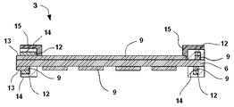
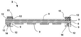
- the film sensor 3 of the present invention has a transparent base sheet 6 and transparent electrodes formed on both sides of the base sheet 6 so as to have the electrode pattern 10 of the central window portion 7 and the thin line drawing circuit pattern 11 of the outer frame portion 8 respectively.
- a light-shielding conductive film 12, a transparent conductive film 9, and a light-shielding conductive film 12 are formed on the conductive film 9 and the thin conductive circuit pattern 11 of the transparent conductive film 9.
- a second frame-shaped light shielding layer 15 made of an exposure developer of a color resist material is provided on the peripheral edge of the surface of the formed substrate sheet 6, and the inner edge of the second frame-shaped light shielding layer 15 is the first Inner edge of frame-shaped light shielding layer 5 Those that are located in remote center side.
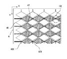
- the electrode pattern 10 formed on the central window 7 of the film sensor 3 will be supplementarily described.
- the electrode pattern 10 has different patterns on the front and back sides.
- the plurality of rhombus electrodes 46 and the connection wiring 469 are electrically connected to each other. Further, such a connection wiring 469 and a plurality of rhombus electrodes 46 penetrating therethrough are taken as a set, and the set is repeatedly arranged in the horizontal direction (X direction) in the drawing.
- connection wiring 479 is different from that of the connection wiring 469 in the horizontal direction (X direction) in the drawing.
- the direction in which a set of the connection wiring 479 and the plurality of rhombus electrodes 47 penetrating the connection wiring 479 is repeatedly arranged is the vertical direction (Y direction) in the drawing.
- the rhombus electrode 46 is disposed so as to fill the gaps between the plurality of connection wirings 479, while the rhombus electrode 47 is disposed so as to fill the gaps between the plurality of connection wirings 469. Is done. Further, in FIG. 5, the positional relationship between the diamond electrode 46 and the diamond electrode 47 is complementary. That is, the plurality of rhombus electrodes 47 are arranged so as to fill in the rhombus-shaped gaps that occur when the rhombus electrodes 46 are arranged in a matrix.
- the X direction electrode and the Y direction electrode are arranged so as to form a lattice in plan view, so that if a user's finger or the like touches any position on the lattice via the cover glass 2 (for example, a capacitor is formed between the finger and the X-direction electrode touched by the finger or the like, and a capacitor is formed between the finger or the Y-direction electrode touched by the finger or the like. .
- a capacitor is formed between the finger and the X-direction electrode touched by the finger or the like
- a capacitor is formed between the finger or the Y-direction electrode touched by the finger or the like.
- the position detector of the external circuit detects the amount of change in capacitance that occurs in such a case, or even the X-direction electrode and Y-direction electrode having the maximum capacitance, and touches anywhere in the central window portion 7. Can be acquired as a set of an X coordinate value and a Y coordinate value as a specific value.
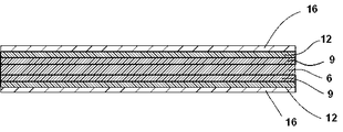
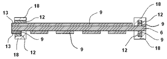
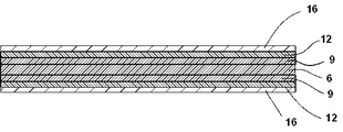
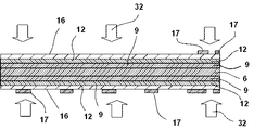
- ⁇ Patterning of transparent conductive film 9 First, transparent conductive films 9 and 9, light-shielding conductive films 12 and 12, and first photoresist layers 16 and 16 were sequentially formed on the front and back surfaces of the transparent substrate sheet 6 to obtain a conductive sheet (FIG. 3 (a)), a mask 17 having a desired pattern is placed on each of the front and back sides, and exposure (see FIG. 3B) and development are performed to pattern the first photoresist layer 16. Note that the position of the mask 17 shown in FIG. 3B is the case where the first photoresist layer 16 is a negative type (when exposed, the solubility in the developer is lowered and the exposed portion remains after development). Show. In the case of the positive type (when exposed, the solubility in the developer increases and the exposed portion is removed), the portion shielded from light by the mask is reversed.
- Examples of the base sheet 6 include plastic films such as polyester resins, polystyrene resins, olefin resins, polybutylene terephthalate resins, polycarbonate resins, and acrylic resins.
- the transparent conductive film 9 includes a layer made of a metal oxide such as indium tin oxide or zinc oxide, and may be formed by a vacuum deposition method, a sputtering method, an ion plating method, a plating method, or the like. Further, the transparent conductive film 9 is formed with a thickness of about several tens to several hundreds nm, and is easily etched together with the light-shielding conductive film 12 in a solution such as ferric chloride, but hydrogen peroxide in an acidic atmosphere. It is necessary that the etching solution for the light-shielding conductive film 12 such as water is not easily etched. And it is preferable to show a light transmittance of 80% or more and a surface resistance value of several m ⁇ to several hundred ⁇ .
- Examples of the light-shielding conductive film 12 include a single metal film having high conductivity and good light-shielding properties, and a layer made of an alloy or a compound thereof, such as a vacuum deposition method, a sputtering method, an ion plating method, and a plating method. It is good to form with. Further, the light-shielding conductive film 12 needs to have an etchant that is not etched by the transparent conductive film 9 but the light-shielding conductive film 12 itself is etched. Examples of the preferable metal include aluminum, nickel, copper, silver, and tin.
- a metal film made of copper foil having a thickness of 20 to 1000 nm is very preferable because it is excellent in conductivity and light shielding properties, and the transparent conductive film can be easily etched with hydrogen peroxide solution even in an acidic atmosphere where etching is not performed. More preferably, the thickness is 30 nm or more. More preferably, the thickness is 100 to 500 nm. This is because a highly conductive light-shielding conductive film 12 can be obtained by setting the thickness to 100 nm or more, and a light-shielding conductive film 12 that is easy to handle and excellent in workability can be obtained by setting the thickness to 500 nm or less.
- the first photoresist layer 16 is made of an acrylic photoresist material having a thickness of 10 to 20 ⁇ m that can be exposed to a high pressure mercury lamp, an ultrahigh pressure mercury lamp, a laser beam or a metal halide lamp and developed with an alkaline solution.
- the first photoresist layer 16 may be formed by a general printing method such as gravure, screen, and offset, as well as by various coater methods, coating and dipping methods, and various methods such as a dry film resist method. Although patterning may be performed by exposure and development, the dry film resist method is more preferable.
- the dry film resist (DFR) used in the dry film resist method is a film in which the above-described photosensitive layer serving as each photoresist layer is sandwiched between a base film and a cover film.
- the above printing method, coating method, painting method, etc. have problems such as only one side coating and poor efficiency, whereas the dry film resist method bonds the photosensitive layer with a heating roll after peeling the cover film.
- This method is mainstream because it is highly productive and can meet various requirements.
- the exposure is usually performed by placing a mask on the base film (not shown), and development is performed after the base film is peeled off.
- As the base film of the dry film resist a film made of polyethylene terephthalate or the like can be used. Moreover, what consists of polyethylene etc. can be used as a cover film of a dry film resist.
- the base sheet 6 made of a plastic film has a problem of elongation. Therefore, the patterning of the first photoresist layer 16 on both sides of the conductive sheet is preferably performed by double-sided simultaneous exposure as in the present invention. This is because when the patterning of the first photoresist layer 16 is performed by exposing one side at a time, the patterning on one side is finished, and the base sheet 6 is stretched when the conductive sheet is replaced with the front and back sides of the exposure apparatus. This is because the pattern on the front surface and the pattern on the back surface will be misaligned. In the case of the example shown in FIG. 5, the arrangement relationship between the rhombus electrode 46 and the rhombus electrode 47 is complementary. Therefore, if the front surface pattern and the back surface pattern are misaligned, the film sensor 3 does not function correctly.
- the pattern of the first photoresist layer 16 on the opposite side is affected even if exposure is performed simultaneously with a different mask pattern. Does not affect. Therefore, since both sides can be exposed simultaneously, the front and back of the first photoresist layer 16 can be easily aligned, and both sides can be patterned in a single process, and the productivity is improved.
- the well-known mask alignment method of a double-sided exposure apparatus can be used for alignment of a front mask and a back mask.
- a mask alignment mark is formed on each of the front mask and the back mask, and an optical reading sensor such as a camera reads the overlapping state of the pair of mask alignment marks, thereby relative to the front mask and the back mask. Get location information. Then, based on the obtained position information, the mask position adjusting mechanism relatively moves the front mask and the back mask so that the pair of mask alignment marks overlap with each other. For example, a method of aligning the back mask.
- the transparent conductive films 9 and 9 and the light-shielding conductive films 12 and 12 are simultaneously etched with an etching solution such as ferric chloride, so that the patterned first photoresist layers 16 and 16 are not stacked.
- an etching solution such as ferric chloride
- the formed electrode pattern 10 is formed, and the thin line drawing circuit pattern 11 in which the transparent conductive films 9 and 9 and the light-shielding conductive films 12 and 12 are laminated without misalignment is formed on the outer frame portions 8 on both sides of the base sheet. (See FIG. 3C).
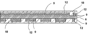
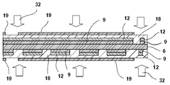
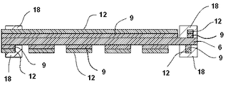
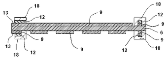
- the first photoresist layers 16 and 16 are stripped with a resist stripping solution to expose the light-shielding conductive films 12 and 12, and then second photoresist layers 18 and 18 are formed on both surfaces (FIG. 3). (See (d)). Thereafter, masks 19 and 19 are placed, exposed (see FIG. 3E) and developed to pattern the second photoresist layer 18 (see FIG. 3F). Note that the position of the mask 19 shown in FIG. 3 (e) is the case where the second photoresist layer 18 is a negative type (when exposed, the solubility with respect to the developer decreases, and the exposed portion remains after development). Show. Further, the material and the formation method of the second photoresist layer 18 can be the same material and the formation method as the first photoresist layer 16.
- the transparent conductive films 9 and 9 are exposed at the central window portion 7 on both sides of the base sheet and the terminal portion 25 in the outer frame portion 8 (see FIGS. 3G and 4).
- the thin line drawing circuit pattern 11 formed on the surface of the substrate 6 is drawn with the laminated portion of the light-shielding conductive film 12 in black and the exposed portion of the transparent conductive film 9 in white, and both ends of the black portion. Coincides with the boundary with the central window portion 7 and the boundary 2 with the terminal portion 13.
- the light-shielding conductive film 12 is laminated on the fine line routing circuit pattern 11 with the same width as that of the fine line routing circuit pattern 11.
- the frame-shaped light shielding layer 15 cannot be substituted.
- the transparent conductive film 9 is an amorphous material, it is preferably crystallized by a method such as heat treatment before the etching. This is because the etching resistance is improved by crystallization, and only the light-shielding metal film 12 can be easily etched selectively.
- the third photoresist layer 28 having rust prevention property the same photoresist material as that of the first photoresist layer 16 with a rust inhibitor added thereto is used, or the above-described photoresist material makes the rust prevention property. A good one should be used.
- the method for forming the third photoresist layer 28 can be the same as the method for forming the first photoresist layer 16.
- the rust preventive agent a material that is already used as a rust preventive agent is used. As specific examples, for example, imidazole, triazole, benzotriazole, benzimidazole, benzthiazole, pyrazole and the like may be used.
- monocyclic or polycyclic azoles such as halogen, alkyl, and phenyl-substituted products, aromatic amines such as aniline, aliphatic amines such as alkylamine, salts thereof, and the like.
- aromatic amines such as aniline
- aliphatic amines such as alkylamine, salts thereof, and the like.
- the anticorrosive functional layer 14 is formed in this way, even if corrosive liquid from the outside enters, or even under an environmental test such as high temperature and high humidity, the routing circuit does not proceed with corrosion, and the electrical characteristics Can be maintained.
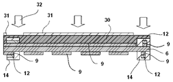
- a fourth photoresist layer 30 made of a color resist material was formed on the entire surface only (see FIG. 3 (k)). Thereafter, masks 31 and 31 are placed, exposed (see FIG. 3 (l)) and developed to pattern the fourth photoresist layer 30, which is used as the second frame-shaped light shielding layer 15 (FIG. 3 (m)). reference). Note that the position of the mask 31 shown in FIG. 3 (l) is the case where the fourth photoresist layer 30 is a negative type (when exposed, the solubility in the developer is lowered and the exposed portion remains after development). Show.
- the second frame-shaped light shielding layer 15 is formed by a photo process as shown in FIGS. 3K to 3M, the linearity of the inner edge is very good.
- the inner edge of the second frame-shaped light-shielding layer 15 is configured to be located closer to the center than the inner edge of the first frame-shaped light-shielding layer 5 of the cover glass 2 formed by screen printing. Therefore, the effect that the outline of the display screen viewed through the cover glass 2 looks sharp can be obtained.
- the difference between the inner edge dimension of the second frame-shaped light shielding layer 15 and the inner frame edge dimension of the first frame-shaped light shielding layer 5 is preferably 0.1 mm to 0.3 mm.
- the same materials as those for resists such as RGB and black matrix constituting a color filter for liquid crystal display can be applied. Further, the fourth photoresist layer 30 can be formed in the same manner as the first photoresist layer 16.
- the reason for not forming the first frame-shaped light shielding layer 5 of the cover glass 2 by the photo process using the color resist material instead of the second frame-shaped light shielding layer 15 by the photo process using the color resist material, the reason for not forming the first frame-shaped light shielding layer 5 of the cover glass 2 by the photo process using the color resist material. explain. Certainly, if the first frame-shaped light-shielding layer 5 of the cover glass 2 is formed by a photo process using a color resist material, it is also possible to obtain linearity at the inner edge of the first frame-shaped light-shielding layer 5. Let's go. However, when the photo process is performed on the cover glass 2, the application, exposure, and development of the color resist material must be performed for each glass substrate 4.
- the size of the glass substrate 4 is limited, and as the size increases, the weight increases and handling becomes difficult. There is also a problem that a coating machine, an exposure machine, and a developing machine suitable for the large-sized glass substrate 4 are required. This is not suitable for mass production and leads to cost increase.
- the photo sensor is performed in the film sensor 3 as in the present invention, the second frame-shaped light shielding layer 15 can be obtained at a relatively high speed by roll-to-roll.
- the color of the second frame-shaped light shielding layer 15 is the same color or similar to the color near the inner edge of the first frame-shaped light shielding layer 5 of the cover glass 2, the first frame-shaped light shielding layer 5 is exposed.
- the boundary between the portion, the laminated portion of the first frame-shaped light-shielding layer 5 and the second frame-shaped light-shielding layer 15 is inconspicuous, and an effect that it looks assimilated is obtained.
- the color difference ⁇ E in the system is preferably 10 or less.
- the color of the second frame-shaped light shielding layer 15 is black or white, an effect of increasing the contrast of the display screen can be obtained.
- the distance between the back surface of the glass substrate 4 and the second frame-shaped light shielding layer 15 is more preferably 10 ⁇ m to 100 ⁇ m. If it is less than 10 ⁇ m, the thickness of the transparent pressure-sensitive adhesive layer becomes thin and the adhesion between the film sensor and the cover glass becomes low, and if it exceeds 100 ⁇ m, the external sense of unity surrounding the display screen becomes low.
- the thickness of the first frame-shaped light shielding layer 5 is 7 ⁇ m to 30 ⁇ m, and the thickness of the second frame-shaped light shielding layer 15 is 2 ⁇ m to 25 ⁇ m.
- the upper limit when the upper limit is exceeded, the level difference between the non-formed part becomes large and bubbles (bubbles) are likely to be generated when pasting. Further, if both of them do not satisfy the lower limit value, it is difficult to obtain a light-shielding property even by a laminated structure, and film production becomes difficult.
- the present invention is not limited to this.
- the second frame-shaped light shielding layer 15 is formed as a separate layer in addition to the transparent conductive film 9, the light-shielding conductive film 12 and the rust prevention functional layer 14.
- the light shielding layer 15 may also be used as a rust prevention functional layer (see the second embodiment below).
- FIG. 8 is an exploded sectional view showing an embodiment of the cover glass integrated sensor according to the present invention.
- 1 is a cover glass integrated sensor
- 2 is a cover glass
- 3 is a film sensor 4 is a glass substrate
- 5 is a first frame-shaped light shielding layer
- 6 is a base sheet
- 7 is a central window portion
- 8 is an outer frame.
- Part, 9 is a transparent conductive film
- 10 is an electrode pattern
- 11 is a thin line drawing circuit pattern
- 12 is a light-shielding conductive film
- 13 is a terminal part
- 14 is a rust prevention functional layer
- 15 is a second frame-shaped light shielding layer (also serving as Rust prevention functional layer) is shown respectively.
- the film sensor 3 of the second embodiment includes a transparent base sheet 6, and an electrode pattern 10 of the central window portion 7 and a thin line drawing circuit pattern of the outer frame portion 8 on both sides of the base sheet 6, respectively.
- Transparent conductive films 9, 9 formed so as to have 11, and light-shielding conductive films 12, 12 laminated on the thin conductive circuit pattern 11 of the transparent conductive film 9 with the same width as the thin conductive circuit pattern 11, respectively.
- the rust prevention functional layer 15 on the surface side is made of an exposure developed product of a color resist material and functions as a second frame-shaped light shielding layer, and the inner edge of the second frame-shaped light shielding layer 15 is the first frame. Center from the inner edge of the light shielding layer 5 It is one that is located in. That is, it is the same as the film sensor 3 of the first embodiment except that the rust prevention functional layer also serves as the second frame-shaped light shielding layer.
- the transparent conductive film 9 and the light-shielding conductive film 12 are simultaneously etched with an etchant such as ferric chloride, and the transparent conductive film 9 in the portion where the patterned first photoresist layers 16 are not laminated. , 9 and the light-shielding conductive films 12, 12, so that the transparent conductive films 9, 9 and the light-shielding conductive films 12, 12 are laminated without misalignment on the central window 7 on both sides of the base sheet, respectively.
- 10 and thin line drawing circuit pattern 11 in which transparent conductive films 9, 9 and light-shielding conductive films 12, 12 are laminated without displacement on outer frame portions 8 on both sides of the base sheet are formed (FIG. 9 ( c)).
- the second photoresist layers 18 and 18 are stripped with a resist stripping solution, and the light-shielding conductive films 12 and 12 laminated with the same width as the thin line-drawing circuit pattern 11 are exposed on the thin-line drawing circuit pattern 11.
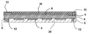
- a third photoresist layer 28 having rust resistance is formed on the entire back surface, and a fourth photoresist layer 30 made of a color resist material having rust resistance is formed on the entire surface (FIG. 9 (h)). reference).
- masks 29 and 29 are placed, exposed (see FIG.
- the third photoresist layer 28 having rust prevention property the same photoresist material as that of the first photoresist layer 16 with a rust inhibitor added thereto is used, or the above-described photoresist material makes the rust prevention property. A good one should be used.
- the method for forming the third photoresist layer 28 can be the same as the method for forming the first photoresist layer 16.
- the rust preventive agent a material that is already used as a rust preventive agent is used. As specific examples, for example, imidazole, triazole, benzotriazole, benzimidazole, benzthiazole, pyrazole and the like may be used.
- monocyclic or polycyclic azoles such as halogen, alkyl, and phenyl-substituted products, aromatic amines such as aniline, aliphatic amines such as alkylamine, salts thereof, and the like.
- aromatic amines such as aniline
- aliphatic amines such as alkylamine, salts thereof, and the like.
- the fourth photoresist layer 30 made of a color resist material having rust preventive properties is added with the above-mentioned rust preventive agent in the same color resist material as RGB and black matrix resists constituting a color filter for liquid crystal display. It is preferable to use a color resist material having excellent rust prevention properties. Further, the fourth photoresist layer 30 can be formed in the same manner as the first photoresist layer 16.
- the second frame-shaped light shielding layer 15 which also serves as the rust prevention functional layer 14 and the rust prevention functional layer is formed, even if corrosive liquid enters from the outside or an environmental test such as high temperature and high humidity. Even underneath, corrosion does not progress in the routing circuit, and electrical characteristics can be maintained.
- the base sheet 6 is not limited to the one constituted by a single plastic film as shown in the figure, and a laminate may be formed by stacking a plurality of plastic films.
- a plastic film laminating means thermal lamination, dry lamination via an adhesive layer, or the like can be used.
- the thickness of the entire laminate can be adjusted by using an adhesive layer having a core material.
- the plastic film may be laminated at any timing after the transparent conductive film 9 is formed on the plastic film, after the light-shielding conductive film 12 is laminated, or after the first photoresist layer 16 is laminated.
- both ends of the laminated portion (black portion in FIG. 4) of the light-shielding conductive film 12 may be set back from the boundary with the central window portion 7 and the boundary 2 with the terminal portion 13. In this case, both ends of the light-shielding conductive film 12 can be protected by the rust prevention functional layer 14 laminated so as to cover the outer frame portion 8 in a later step.
- Example 1 A colorless polyester film having a thickness of 200 ⁇ m unwound from a roll is used as a base sheet, a transparent conductive film is formed with a thickness of 200 nm by sputtering made of indium tin oxide, and a copper film is formed thereon as a light-shielding conductive film Was formed by sputtering to a thickness of 500 nm to prepare a conductive film. Then, after laminating a set of conductive films using a transparent adhesive to obtain a laminate in which a transparent conductive film and a light-shielding conductive film are laminated on both sides, a negative type that can be developed with a 1% sodium carbonate solution.
- a first photoresist layer having a thickness of 10 nm is formed on both surfaces of the laminate, and a mask having an X-direction electrode pattern is placed on the front side.
- a mask having an electrode pattern in the Y direction was placed, and both front and back surfaces were exposed simultaneously by a metal halide lamp, and developed by being immersed in a 1% sodium carbonate solution.
- the portion of the indium tin oxide film and the copper film where the patterned first photoresist layer is not laminated is simultaneously etched away with an etching solution of ferric chloride. Is an electrode pattern in the X direction, and a Y direction electrode pattern is exposed on the back side, and a thin line drawing pattern with an average line width of 20 ⁇ m is exposed on both the front and back surfaces on the outer frame surrounding the central window. It had been.
- a dry film resist that can be developed with a 1% sodium carbonate solution and has a negative type acrylic photosensitive layer is used, and a second photoresist layer having a thickness of 10 nm is formed on both surfaces.
- a mask was placed on the outer frame portion excluding the front and back terminal portions, and both the front and back surfaces were exposed simultaneously by a metal halide lamp, and developed by being immersed in a 1% sodium carbonate solution.
- a third photoresist layer having a thickness of 10 nm is formed on both surfaces, and a mask is placed on the outer frame portion excluding the terminal portion, and both the front and back surfaces are exposed simultaneously by a metal halide lamp, and immersed in 1% sodium carbonate solution.
- the remaining third photoresist layer was used as a rust prevention functional layer.
- a fourth photoresist layer having a thickness of 5 ⁇ m is formed on the entire surface using a dry film resist that can be developed with a 1% sodium carbonate solution and has a negative acrylic photosensitive layer made of a black color resist material. Then, a mask is placed thereon, only the surface is exposed by a metal halide lamp, developed by being immersed in a 1% sodium carbonate solution, and the remaining black fourth photoresist layer is used as a second frame-shaped light shielding layer, Next, one film sensor was cut.
- a cover glass was obtained by forming a first frame-shaped light-shielding layer having a thickness of 7 ⁇ m by screen printing using black ink on the peripheral edge of the back surface of a glass substrate made of borosilicate glass having a thickness of 0.7 mm. .
- the previous film sensor was bonded with a transparent adhesive on the back surface of the cover glass to form a cover glass integrated sensor.
- the inner edge of the second frame-shaped light-shielding layer is located at the center side by 0.1 mm from the inner edge of the first frame-shaped light-shielding layer.
- the distance from the frame-shaped light shielding layer was 25 ⁇ m.
- the cover glass integrated sensor has a sharp outline of the display screen viewed through the cover glass, is excellent in visibility, and has a sense of unity in appearance at a portion surrounding the display screen.
- Example 2 A colorless polyester film having a thickness of 200 ⁇ m unwound from a roll is used as a base sheet, a transparent conductive film is formed with a thickness of 200 nm by sputtering made of indium tin oxide, and a copper film is formed thereon as a light-shielding conductive film Was formed by sputtering to a thickness of 500 nm to prepare a conductive film.
- a negative type that can be developed with a 1% caustic soda solution.
- a dry film resist provided with an acrylic photosensitive layer
- a first photoresist layer having a thickness of 10 nm is formed on both sides of the laminate, and a mask having an X-direction electrode pattern is placed on the front side
- a mask having an electrode pattern in the Y direction was placed on the back side, and both the front and back surfaces were exposed simultaneously by a metal halide lamp, and developed by immersion in a 1% caustic soda solution.
- the portion of the indium tin oxide film and the copper film where the patterned first photoresist layer is not laminated is simultaneously etched away with an etching solution of ferric chloride. Is an electrode pattern in the X direction, and a Y direction electrode pattern is exposed on the back side, and a thin line drawing pattern with an average line width of 20 ⁇ m is exposed on both the front and back surfaces on the outer frame surrounding the central window. It had been.
- a 10 nm thick second photoresist layer is formed on both surfaces using a dry film resist that can be developed with 1% caustic soda solution and has a negative acrylic photosensitive layer. Then, a mask was placed on the outer frame portion excluding the terminal portions on the front and back sides, and both the front and back surfaces were exposed simultaneously with a metal halide lamp, and developed by immersion in 1% caustic soda solution.
- a dry film resist provided with a negative type acrylic photosensitive layer which can be developed with a 1% caustic soda solution and benzoimidar is added as a rust inhibitor on the back surface.
- a negative type acrylic system in which a third photoresist layer having a thickness of 10 nm is formed on the entire surface, which can be developed with a 1% caustic soda solution on the surface, and benzoimidar is added as a rust preventive to a black color resist material.
- a dry film resist with a photosensitive layer a 5 ⁇ m-thick fourth photoresist layer is formed on the entire surface, and a mask is placed on the outer frame part except for the terminal part on each side.
- Both sides are exposed at the same time, soaked in a 1% caustic soda solution and developed, and the remaining third photoresist layer is treated as an anticorrosive function layer and the remaining black fourth photo.
- the resist layer is a second frame-shaped light shielding layer, and then cutting the film sensor one minute.
- a cover glass was obtained by forming a first frame-shaped light-shielding layer having a thickness of 7 ⁇ m by screen printing using black ink on the peripheral edge of the back surface of a glass substrate made of borosilicate glass having a thickness of 0.7 mm. .
- the previous film sensor was bonded with a transparent adhesive on the back surface of the cover glass to form a cover glass integrated sensor.
- the inner edge of the second frame-shaped light-shielding layer is located at the center side by 0.1 mm from the inner edge of the first frame-shaped light-shielding layer.
- the distance from the frame-shaped light shielding layer was 25 ⁇ m.
- the cover glass integrated sensor has a sharp outline of the display screen viewed through the cover glass, is excellent in visibility, and has a sense of unity in appearance at a portion surrounding the display screen.
- the present invention relates to PDAs, handheld terminals and other portable information terminals, copiers, OA devices such as facsimiles, smartphones, mobile phones, portable game devices, electronic dictionaries, car navigation systems, small PCs, digital cameras, video cameras, portable MDs (PMDs).
- OA devices such as facsimiles, smartphones, mobile phones, portable game devices, electronic dictionaries, car navigation systems, small PCs, digital cameras, video cameras, portable MDs (PMDs).
- PMDs portable MDs
Landscapes
- Engineering & Computer Science (AREA)
- General Engineering & Computer Science (AREA)
- Theoretical Computer Science (AREA)
- Human Computer Interaction (AREA)
- Physics & Mathematics (AREA)
- General Physics & Mathematics (AREA)
- Position Input By Displaying (AREA)
- Solid State Image Pick-Up Elements (AREA)
- Laminated Bodies (AREA)
Abstract
Description
前記カバーガラスの裏面に貼り合わせられた静電容量方式のフィルムセンサーとを備えたカバーガラス一体型センサーであって、
前記フィルムセンサーが、
透明な基体シートと、
前記基体シートの両面に各々、中央窓部の電極パターンおよび外枠部の細線引き回し回路パターンを有するように形成された透明導電膜と
前記透明導電膜の前記細線引き回し回路パターン上に各々、当該細線引き回し回路パターンと同一幅で積層された遮光性導電膜と、
前記透明導電膜及び前記遮光性導電膜が形成された前記基体シートの両面に各々、端子部以外の前記外枠部を覆うように積層された防錆機能層と、
を備えたものであり、
さらに前記フィルムセンサーが、前記基体シートの表面周縁部に形成された、カラーレジスト材料の露光現像物からなる第二の枠状遮光層を有し、かつ、当該第二の枠状遮光層の内縁が、前記第一の枠状遮光層の内縁よりも中央側に位置している、
ことを特徴とするカバーガラス一体型センサーを提供する。
以下、図面を参照しながら本発明の第一実施形態について詳細に説明する。図1は本発明に係るカバーガラス一体型センサーの一実施例を示す分解断面図であり、図2は本発明に係るカバーガラス一体型センサーの一実施例を示す平面図である。図中、1はカバーガラス一体型センサー、2はカバーガラス、3はフィルムセンサー4はガラス基板、5は第一の枠状遮光層、6は基体シート、7は中央窓部、8は外枠部、9は透明導電膜、10は電極パターン、11は細線引き回し回路パターン、12は遮光性導電膜、13は端子部、14は防錆機能層、15は第二の枠状遮光層をそれぞれ示す。
まず、透明な基体シート6の表裏両面に各々、透明導電膜9,9、遮光性導電膜12,12、第一フォトレジスト層16,16を順次全面形成して導電性シートを得た(図3(a)参照)後、表裏それぞれ所望のパターンのマスク17を載せ、露光(図3(b)参照)・現像して第一フォトレジスト層16をパターン化する。なお、図3(b)に示すマスク17の位置は、第一フォトレジスト層16がネガ型(露光されると現像液に対して溶解性が低下し、現像後に露光部分が残る)の場合を示している。ポジ型(露光されると現像液に対して溶解性が増大し、露光部が除去される)の場合にはマスクで遮光する部分が逆になる。
次に、レジスト剥離液でもって第一フォトレジスト層16,16を剥離し、遮光性導電膜12,12を露出させた後、両面に第二フォトレジスト層18,18を全面形成した(図3(d)参照)。その後、マスク19,19を載せ、露光(図3(e)参照)・現像して第二フォトレジスト層18をパターン化する(図3(f)参照)。なお、図3(e)に示すマスク19の位置は、第二フォトレジスト層18がネガ型(露光されると現像液に対して溶解性が低下し、現像後に露光部分が残る)の場合を示している。また、第二フォトレジスト層18の材料及び形成方法は、第一フォトレジスト層16と同様の材料及び形成方法とすることができる。
次いで、レジスト剥離液でもって第二フォトレジスト層18,18を剥離し、細線引き回し回路パターン11上に細線引き回し回路パターン11と同一幅で積層された遮光性導電膜12,12を露出させた後、防錆性を有する第三フォトレジスト層28,28を全面形成した(図3(h)参照)。その後、マスク29,29を載せ、露光(図3(i)参照)・現像して第三フォトレジスト層28,28をパターン化し、これを防錆機能層14,14とした(図3(j)参照)。なお、図3(i)に示すマスク29の位置は、第三フォトレジスト層28がネガ型(露光されると現像液に対して溶解性が低下し、現像後に露光部分が残る)の場合を示している。
最後に、カラーレジスト材料からなる第四フォトレジスト層30を表面のみに全面形成した(図3(k)参照)。その後、マスク31,31を載せ、露光(図3(l)参照)・現像して第四フォトレジスト層30をパターン化し、これを第二の枠状遮光層15とした(図3(m)参照)。なお、図3(l)に示すマスク31の位置は、第四フォトレジスト層30がネガ型(露光されると現像液に対して溶解性が低下し、現像後に露光部分が残る)の場合を示している。
以下、図面を参照しながら本発明の第二実施形態について詳細に説明する。図8は本発明に係るカバーガラス一体型センサーの一実施例を示す分解断面図である。図中、1はカバーガラス一体型センサー、2はカバーガラス、3はフィルムセンサー4はガラス基板、5は第一の枠状遮光層、6は基体シート、7は中央窓部、8は外枠部、9は透明導電膜、10は電極パターン、11は細線引き回し回路パターン、12は遮光性導電膜、13は端子部、14は防錆機能層、15は第二の枠状遮光層(兼防錆機能層)をそれぞれ示す。
まず、透明な基体シート6の表裏両面に各々、透明導電膜9,9、遮光性導電膜12,12、第一フォトレジスト層16,16を順次全面形成して導電性シートを得た(図9(a)参照)後、表裏それぞれ所望のパターンのマスク17,17を載せ、露光(図9(b)参照)・現像して第一フォトレジスト層16,16をパターン化する。
次に、レジスト剥離液でもって第一フォトレジスト層16,16を剥離し、遮光性導電膜12,12を露出させた後、両面に第二フォトレジスト層18,18を全面形成した(図9(d)参照)。その後、マスク19,19を載せ、露光(図9(e)参照)・現像して第二フォトレジスト層18,18をパターン化する(図9(f)参照)。
次いで、レジスト剥離液でもって第二フォトレジスト層18,18を剥離し、細線引き回し回路パターン11上に細線引き回し回路パターン11と同一幅で積層された遮光性導電膜12,12を露出させた後、裏面には防錆性を有する第三フォトレジスト層28を全面形成し、表面には防錆性を有しカラーレジスト材料からなる第四フォトレジスト層30を全面形成した(図9(h)参照)。その後、マスク29,29を載せ、露光(図9(i)参照)・現像して第三フォトレジスト層28および第四フォトレジスト層30をパターン化し、それぞれ防錆機能層14、防錆機能層を兼ねる第二の枠状遮光層15とした(図9(j)参照)。なお、図9(i)に示すマスク29の位置は、第三フォトレジスト層28および第四フォトレジスト層30がネガ型(露光されると現像液に対して溶解性が低下し、現像後に露光部分が残る)の場合を示している。
また、基体シート6は、図示したようなプラスチックフィルム単層で構成するものに限定されず、プラスチックフィルムを複数枚重ねて積層体を基体シート6としてもよい。この場合、プラスチックフィルムの積層手段としては熱ラミネートや接着剤層を介したドライラミネートなどが挙げられる。接着剤層にてプラスチックフィルムを積層する場合、接着剤層として芯材を有するものを用いて積層体全体の厚み調整をすることもできる。また、プラスチックフィルムの積層は、プラスチックフィルム上への透明導電膜9の形成後、遮光性導電膜12の積層後または第一フォトレジスト層16の積層後のいずれのタイミングで行ってもよい。
ロールから巻き出した厚さ200μmの無色ポリエステルフィルムを基体シートとし、その片面に透明導電膜としてインジウムスズ酸化物からなるスパッタリング法で200nmの厚みで形成し、その上に遮光性導電膜として銅膜をスパッタリング法で500nmの厚みで形成して導電性フィルムを用意した。次いで、一組の導電性フィルムを透明粘着剤を用いてラミネートし、両面に透明導電膜及び遮光性導電膜を各々積層した積層体を得た後に、炭酸ソーダ1%液で現像が可能なネガタイプのアクリル系感光層を備えたドライフィルムレジストを用い、厚み10nmの第一フォトレジスト層を前記積層体の両面に各々、全面形成し、表側にはX方向の電極パターンを有するマスクを載置し、裏側にはY方向の電極パターンを有するマスクを載置して、メタルハライドランプによって表裏両面同時に露光し、炭酸ソーダ1%液に浸して現像した。
ロールから巻き出した厚さ200μmの無色ポリエステルフィルムを基体シートとし、その片面に透明導電膜としてインジウムスズ酸化物からなるスパッタリング法で200nmの厚みで形成し、その上に遮光性導電膜として銅膜をスパッタリング法で500nmの厚みで形成して導電性フィルムを用意した。次いで、一組の導電性フィルムを透明粘着剤を用いてラミネートし、両面に透明導電膜及び遮光性導電膜を各々積層した積層体を得た後に、苛性ソーダ1%液で現像が可能なネガタイプのアクリル系感光層を備えたドライフィルムレジストを用い、厚み10nmの第一フォトレジスト層を前記積層体の両面に各々、全面形成し、表側にはX方向の電極パターンを有するマスクを載置し、裏側にはY方向の電極パターンを有するマスクを載置して、メタルハライドランプによって表裏両面同時に露光し、苛性ソーダ1%液に浸して現像した。
2 カバーガラス
3 フィルムセンサー
4 ガラス基板
5 第一の枠状遮光層
6 透明な基体シート
7 中央窓部
8 外枠部
9 透明導電膜
10 電極パターン
11 細線引き回し回路パターン
12 遮光性導電膜
13 端子部
14 防錆機能層
15 第二の枠状遮光層
16 第一フォトレジスト層
17 マスク
18 第二フォトレジスト層
19 マスク
28 第三フォトレジスト層
29 マスク
30 第四フォトレジスト層
31 マスク
46,47 菱形電極
469.479 接続配線
Claims (9)
- 透明なガラス基板の裏面周縁部にスクリーン印刷膜からなる第一の枠状遮光層が形成された電子機器表示窓のカバーガラスと、
前記カバーガラスの裏面に貼り合わせられた静電容量方式のフィルムセンサーとを備えたカバーガラス一体型センサーであって、
前記フィルムセンサーが、
透明な基体シートと、
前記基体シートの両面に各々、中央窓部の電極パターンおよび外枠部の細線引き回し回路パターンを有するように形成された透明導電膜と
前記透明導電膜の前記細線引き回し回路パターン上に各々、当該細線引き回し回路パターンと同一幅で積層された遮光性導電膜と、
前記透明導電膜及び前記遮光性導電膜が形成された前記基体シートの両面に各々、端子部以外の前記外枠部を覆うように積層された防錆機能層と、
を備えたものであり、
さらに前記フィルムセンサーが、前記基体シートの表面周縁部に形成された、カラーレジスト材料の露光現像物からなる第二の枠状遮光層を有し、かつ、当該第二の枠状遮光層の内縁が、前記第一の枠状遮光層の内縁よりも中央側に位置している、
ことを特徴とするカバーガラス一体型センサー。 - 前記第二の枠状遮光層が、前記透明導電膜、前記遮光性導電膜及び前記防錆機能層に加えて別層として形成されたものである、請求項1記載のカバーガラス一体型センサー。
- 前記第二の枠状遮光層が、前記防錆機能層を兼ねるものである、請求項1記載のカバーガラス一体型センサー。
- 前記ガラス基板の裏面と前記第二の枠状遮光層との間の距離が10μm~100μmである、請求項1~3のいずれかに記載のカバーガラス一体型センサー。
- 前記第一の枠状遮光層の内縁近傍の色と前記第二の枠状遮光層の色とが同一色又は類似色である、請求項1~4のいずれかに記載のカバーガラス一体型センサー。
- 前記第一の枠状遮光層の内縁近傍の色と前記第二の枠状遮光層の色とのCIE(国際照明委員会)1976(JIS Z8729)のL*a*b*表色系における色差ΔEが10以下である、請求項5記載のカバーガラス一体型センサー。
- 前記第二の枠状遮光層の色が黒色又は白色である、請求項1~6のいずれかに記載のカバーガラス一体型センサー。
- 前記第一の枠状遮光層の厚みが7μm~30μm、前記第二の枠状遮光層の厚みが2μm~25μmである、請求項1~7のいずれかに記載のカバーガラス一体型センサー。
- 前記第二の枠状遮光層の内縁間寸法と前記第一の枠状遮光層の内縁間寸法との差が0.1mm~0.3mmである、請求項1~8のいずれかに記載のカバーガラス一体型センサ
Priority Applications (3)
| Application Number | Priority Date | Filing Date | Title |
|---|---|---|---|
| CN201180058171.4A CN103250121B (zh) | 2010-12-21 | 2011-12-19 | 覆盖玻璃一体型传感器 |
| KR1020137005045A KR101313028B1 (ko) | 2010-12-21 | 2011-12-19 | 커버 유리 일체형 센서 |
| US13/820,044 US8730415B2 (en) | 2010-12-21 | 2011-12-19 | Cover glass integrated sensor |
Applications Claiming Priority (4)
| Application Number | Priority Date | Filing Date | Title |
|---|---|---|---|
| JP2010-285195 | 2010-12-21 | ||
| JP2010-285194 | 2010-12-21 | ||
| JP2010285194A JP5026580B2 (ja) | 2010-12-21 | 2010-12-21 | カバーガラス一体型センサー |
| JP2010285195A JP5026581B2 (ja) | 2010-12-21 | 2010-12-21 | カバーガラス一体型センサー |
Publications (1)
| Publication Number | Publication Date |
|---|---|
| WO2012086596A1 true WO2012086596A1 (ja) | 2012-06-28 |
Family
ID=46313866
Family Applications (1)
| Application Number | Title | Priority Date | Filing Date |
|---|---|---|---|
| PCT/JP2011/079382 Ceased WO2012086596A1 (ja) | 2010-12-21 | 2011-12-19 | カバーガラス一体型センサー |
Country Status (5)
| Country | Link |
|---|---|
| US (1) | US8730415B2 (ja) |
| KR (1) | KR101313028B1 (ja) |
| CN (1) | CN103250121B (ja) |
| TW (1) | TWI431517B (ja) |
| WO (1) | WO2012086596A1 (ja) |
Cited By (4)
| Publication number | Priority date | Publication date | Assignee | Title |
|---|---|---|---|---|
| CN103294263A (zh) * | 2013-04-01 | 2013-09-11 | 友达光电股份有限公司 | 触控显示装置与显示装置 |
| JP2014038531A (ja) * | 2012-08-18 | 2014-02-27 | Kyocera Corp | 入力装置、表示装置、および電子機器 |
| JP2015014976A (ja) * | 2013-07-08 | 2015-01-22 | 日本写真印刷株式会社 | タッチセンサ及びディスプレイ装置 |
| US20150251947A1 (en) * | 2012-09-21 | 2015-09-10 | Saint-Gobain Glass France | Sheet of glass and device including said sheet of glass |
Families Citing this family (28)
| Publication number | Priority date | Publication date | Assignee | Title |
|---|---|---|---|---|
| JP5861641B2 (ja) * | 2010-09-29 | 2016-02-16 | 大日本印刷株式会社 | タッチパネルセンサフィルム及びその製造方法 |
| KR20120072186A (ko) | 2010-12-23 | 2012-07-03 | 엘지이노텍 주식회사 | 터치 패널 및 전극 부재 제조 방법 |
| US9323365B2 (en) * | 2012-10-29 | 2016-04-26 | Google Inc. | Masking an outer perimeter of a touch screen |
| CN103995609A (zh) * | 2013-02-17 | 2014-08-20 | 宸鸿科技(厦门)有限公司 | 触控装置及其形成方法 |
| KR102207861B1 (ko) * | 2013-04-26 | 2021-01-26 | 삼성전자주식회사 | 디스플레이 방법 및 그 방법을 처리하는 전자 장치 |
| CN104571667B (zh) * | 2013-10-26 | 2018-05-29 | 宝宸(厦门)光学科技有限公司 | 触控面板及其制造方法 |
| US9645008B2 (en) | 2014-08-25 | 2017-05-09 | Apple Inc. | Light sensor windows for electronic devices |
| KR20160028595A (ko) * | 2014-09-03 | 2016-03-14 | 삼성디스플레이 주식회사 | 커버 윈도우, 이의 제조 방법 및 이를 포함하는 표시 장치 |
| CN104216565A (zh) * | 2014-09-04 | 2014-12-17 | 上海和辉光电有限公司 | 显示装置及其制作方法 |
| KR102269972B1 (ko) | 2014-10-30 | 2021-06-28 | 삼성디스플레이 주식회사 | 표시 장치 및 그 제조 방법 |
| TW201616467A (zh) | 2014-10-31 | 2016-05-01 | 中華映管股份有限公司 | 曲面裝飾板以及曲面顯示裝置的製作方法 |
| JP6230559B2 (ja) * | 2014-12-03 | 2017-11-15 | 富士フイルム株式会社 | 転写フィルム、フィルムセンサーの製造方法、フィルムセンサー、前面板一体型センサーおよび画像表示装置 |
| TWI564762B (zh) * | 2015-04-22 | 2017-01-01 | 恆顥科技股份有限公司 | 觸控薄膜疊層卷的製作方法與所製得之觸控薄膜疊層片 |
| US9951552B2 (en) | 2015-05-26 | 2018-04-24 | Guardian Glass, LLC | Glazing with heat flux sensor and/or methods of making the same |
| CN104898886A (zh) * | 2015-06-19 | 2015-09-09 | 京东方科技集团股份有限公司 | 一种基板及其制备方法、触控显示屏 |
| US11656552B2 (en) * | 2015-07-16 | 2023-05-23 | Ming-An Hsu | Device having color resists pattern and method for manufacturing the same |
| CN108139838B (zh) * | 2015-10-21 | 2021-05-28 | 富士胶片株式会社 | 透明导电膜、透明导电膜的制造方法以及触控传感器 |
| JP6580153B2 (ja) | 2015-10-26 | 2019-09-25 | 富士フイルム株式会社 | フィルムセンサーの製造方法、前面板一体型センサーの製造方法および画像表示装置の製造方法 |
| US9608023B1 (en) | 2016-05-02 | 2017-03-28 | Omnivision Technologies, Inc. | Edge reflection reduction |
| CN206133508U (zh) * | 2016-08-25 | 2017-04-26 | 合肥鑫晟光电科技有限公司 | 一种触摸屏、显示面板及显示装置 |
| CN108017287A (zh) * | 2016-10-31 | 2018-05-11 | 南昌欧菲光学技术有限公司 | 盖板玻璃层叠结构及其加工方法 |
| US11397498B2 (en) * | 2017-08-30 | 2022-07-26 | Nissha Co., Ltd. | Electrode film and method for manufacturing same |
| TWI645321B (zh) * | 2017-10-17 | 2018-12-21 | 友達光電股份有限公司 | 觸控板 |
| CN110554789B (zh) * | 2018-05-30 | 2023-09-01 | 英属维京群岛商天材创新材料科技股份有限公司 | 双面电极及其图案化方法 |
| CN115202111B (zh) * | 2018-10-16 | 2024-11-12 | 群创光电股份有限公司 | 显示装置 |
| US11831801B2 (en) * | 2020-02-20 | 2023-11-28 | The Light Phone Inc. | Communication device with a purpose-driven graphical user interface, graphics driver, and persistent display |
| CN114741006B (zh) * | 2022-03-23 | 2025-01-28 | 牧东光电科技有限公司 | 一种玻璃sensor及其制备方法 |
| TWI909657B (zh) * | 2024-08-29 | 2025-12-21 | 晨豐光電股份有限公司 | 觸控顯示之玻璃蓋板結構 |
Citations (3)
| Publication number | Priority date | Publication date | Assignee | Title |
|---|---|---|---|---|
| JP2009070191A (ja) * | 2007-09-13 | 2009-04-02 | Nissha Printing Co Ltd | 静電容量センサとその製造方法 |
| JP2009276821A (ja) * | 2008-05-12 | 2009-11-26 | Casio Hitachi Mobile Communications Co Ltd | タッチパネル装置、表示装置、および、端末装置 |
| JP2010515969A (ja) * | 2007-01-05 | 2010-05-13 | アップル インコーポレイテッド | タッチスクリーン積層体 |
Family Cites Families (5)
| Publication number | Priority date | Publication date | Assignee | Title |
|---|---|---|---|---|
| KR970007449A (ja) * | 1995-07-31 | 1997-02-21 | ||
| DE10138759A1 (de) * | 2001-08-07 | 2003-03-06 | Bosch Gmbh Robert | Verfahren zur Herstellung eines Halbleiterbauelements sowie Halbleiterbauelement, insbesondere Membransensor |
| TWI373665B (en) * | 2008-12-25 | 2012-10-01 | Au Optronics Corp | Touch panel structure |
| CN102498462B (zh) * | 2009-09-11 | 2014-11-19 | 日本写真印刷株式会社 | 窄边框触摸输入薄片及其制造方法 |
| CN101799446B (zh) * | 2010-04-16 | 2012-09-12 | 黑龙江大学 | 室温醇类薄膜气体传感器的制备方法 |
-
2011
- 2011-12-19 CN CN201180058171.4A patent/CN103250121B/zh active Active
- 2011-12-19 KR KR1020137005045A patent/KR101313028B1/ko active Active
- 2011-12-19 WO PCT/JP2011/079382 patent/WO2012086596A1/ja not_active Ceased
- 2011-12-19 US US13/820,044 patent/US8730415B2/en active Active
- 2011-12-21 TW TW100147604A patent/TWI431517B/zh not_active IP Right Cessation
Patent Citations (3)
| Publication number | Priority date | Publication date | Assignee | Title |
|---|---|---|---|---|
| JP2010515969A (ja) * | 2007-01-05 | 2010-05-13 | アップル インコーポレイテッド | タッチスクリーン積層体 |
| JP2009070191A (ja) * | 2007-09-13 | 2009-04-02 | Nissha Printing Co Ltd | 静電容量センサとその製造方法 |
| JP2009276821A (ja) * | 2008-05-12 | 2009-11-26 | Casio Hitachi Mobile Communications Co Ltd | タッチパネル装置、表示装置、および、端末装置 |
Cited By (5)
| Publication number | Priority date | Publication date | Assignee | Title |
|---|---|---|---|---|
| JP2014038531A (ja) * | 2012-08-18 | 2014-02-27 | Kyocera Corp | 入力装置、表示装置、および電子機器 |
| US20150251947A1 (en) * | 2012-09-21 | 2015-09-10 | Saint-Gobain Glass France | Sheet of glass and device including said sheet of glass |
| US10071930B2 (en) * | 2012-09-21 | 2018-09-11 | Saint-Gobain Glass France | Sheet of glass and device including said sheet of glass |
| CN103294263A (zh) * | 2013-04-01 | 2013-09-11 | 友达光电股份有限公司 | 触控显示装置与显示装置 |
| JP2015014976A (ja) * | 2013-07-08 | 2015-01-22 | 日本写真印刷株式会社 | タッチセンサ及びディスプレイ装置 |
Also Published As
| Publication number | Publication date |
|---|---|
| US20130153393A1 (en) | 2013-06-20 |
| CN103250121B (zh) | 2014-09-17 |
| KR20130028801A (ko) | 2013-03-19 |
| TWI431517B (zh) | 2014-03-21 |
| CN103250121A (zh) | 2013-08-14 |
| KR101313028B1 (ko) | 2013-10-02 |
| US8730415B2 (en) | 2014-05-20 |
| TW201237708A (en) | 2012-09-16 |
Similar Documents
| Publication | Publication Date | Title |
|---|---|---|
| KR101313028B1 (ko) | 커버 유리 일체형 센서 | |
| JP5026581B2 (ja) | カバーガラス一体型センサー | |
| JP5026580B2 (ja) | カバーガラス一体型センサー | |
| JP5234868B1 (ja) | 光学機能付き静電容量方式タッチセンサー | |
| US8723046B2 (en) | Narrow frame touch input sheet with good anticorrosion property and manufacturing method thereof | |
| KR101586263B1 (ko) | 협액자 터치 입력 시트와 그 제조 방법 | |
| JP4601710B1 (ja) | 狭額縁タッチ入力シートとその製造方法 | |
| JP4855536B1 (ja) | 防錆性に優れたタッチ入力シートの製造方法 | |
| CN101853114A (zh) | 设有电极的电容触摸屏及其制造方法 | |
| CN107003766B (zh) | 转印膜、膜传感器的制造方法、膜传感器、前面板一体型传感器及图像显示装置 | |
| WO2014112323A1 (ja) | 偏光サングラス対応のタッチ機能付偏光板とその製造方法、液晶表示装置 | |
| JP2011129272A (ja) | 両面透明導電膜シートとその製造方法 | |
| JP4870836B1 (ja) | 狭額縁タッチ入力シートの製造方法 | |
| JP4870835B1 (ja) | 狭額縁タッチ入力シートの製造方法 | |
| KR20200018009A (ko) | 메탈메쉬 구조의 터치 패널의 제조 방법 | |
| KR101477072B1 (ko) | 광학 기능이 부가된 정전 용량 방식 터치 센서 |
Legal Events
| Date | Code | Title | Description |
|---|---|---|---|
| 121 | Ep: the epo has been informed by wipo that ep was designated in this application |
Ref document number: 11851172 Country of ref document: EP Kind code of ref document: A1 |
|
| ENP | Entry into the national phase |
Ref document number: 20137005045 Country of ref document: KR Kind code of ref document: A |
|
| WWE | Wipo information: entry into national phase |
Ref document number: 13820044 Country of ref document: US |
|
| NENP | Non-entry into the national phase |
Ref country code: DE |
|
| 122 | Ep: pct application non-entry in european phase |
Ref document number: 11851172 Country of ref document: EP Kind code of ref document: A1 |