WO2012086586A1 - ラマン散乱光増強素子 - Google Patents
ラマン散乱光増強素子 Download PDFInfo
- Publication number
- WO2012086586A1 WO2012086586A1 PCT/JP2011/079360 JP2011079360W WO2012086586A1 WO 2012086586 A1 WO2012086586 A1 WO 2012086586A1 JP 2011079360 W JP2011079360 W JP 2011079360W WO 2012086586 A1 WO2012086586 A1 WO 2012086586A1
- Authority
- WO
- WIPO (PCT)
- Prior art keywords
- scattered light
- raman
- raman scattered
- enhancing element
- electromagnetic field
- Prior art date
- Legal status (The legal status is an assumption and is not a legal conclusion. Google has not performed a legal analysis and makes no representation as to the accuracy of the status listed.)
- Ceased
Links
Images


Classifications
-
- G—PHYSICS
- G02—OPTICS
- G02B—OPTICAL ELEMENTS, SYSTEMS OR APPARATUS
- G02B5/00—Optical elements other than lenses
- G02B5/02—Diffusing elements; Afocal elements
- G02B5/0273—Diffusing elements; Afocal elements characterized by the use
- G02B5/0284—Diffusing elements; Afocal elements characterized by the use used in reflection
-
- G—PHYSICS
- G01—MEASURING; TESTING
- G01N—INVESTIGATING OR ANALYSING MATERIALS BY DETERMINING THEIR CHEMICAL OR PHYSICAL PROPERTIES
- G01N21/00—Investigating or analysing materials by the use of optical means, i.e. using sub-millimetre waves, infrared, visible or ultraviolet light
- G01N21/62—Systems in which the material investigated is excited whereby it emits light or causes a change in wavelength of the incident light
- G01N21/63—Systems in which the material investigated is excited whereby it emits light or causes a change in wavelength of the incident light optically excited
- G01N21/65—Raman scattering
- G01N21/658—Raman scattering enhancement Raman, e.g. surface plasmons
-
- B—PERFORMING OPERATIONS; TRANSPORTING
- B82—NANOTECHNOLOGY
- B82Y—SPECIFIC USES OR APPLICATIONS OF NANOSTRUCTURES; MEASUREMENT OR ANALYSIS OF NANOSTRUCTURES; MANUFACTURE OR TREATMENT OF NANOSTRUCTURES
- B82Y20/00—Nanooptics, e.g. quantum optics or photonic crystals
Definitions
- the present invention relates to a Raman scattered light enhancing element using surface enhanced Raman scattering (SERS).
- SERS surface enhanced Raman scattering
- Raman spectroscopy which obtains a spectrum of Raman scattered light by diffusing Raman scattered light obtained by irradiating an analysis object with light of a single wavelength (laser light), is usually used for identification of substances.
- the Raman scattered light obtained from the analysis object is difficult to detect with high sensitivity because the signal is weak.
- the localized surface plasmon of metal nanoparticles is used to irradiate the analyte to be adsorbed on the surface of the metal nanoparticles with laser light, thereby dramatically enhancing the Raman scattered light generated.
- SERS surface-enhanced Raman scattering
- Patent Document 1 discloses an optical sensor (light enhancement element) configured such that a layer made of silver nanoparticles and a smooth silver film (surface plasmon mirror) are opposed to each other with a dielectric film having a thickness of 40 nm or less interposed therebetween.
- a higher-order enhancement effect of the Raman signal is obtained by the action of the enhanced electromagnetic field generated by the resonance between the localized surface plasmon of the silver nanoparticles and the surface plasmon polariton mode of the smooth silver film.
- a stronger enhancement effect can be obtained by providing a regular periodic structure in the metal nanoparticle layer.
- Patent Document 1 describes that a Raman signal (SERS signal) can be obtained with a very small laser light power of, for example, about 0.4 ⁇ W (up to 10 14 times as an enhancement factor).
- the above laser light source needs to have a high output with an excitation power density per irradiation area as large as about 13,000 mW / cm 2 .
- a Raman analyzer that satisfies the above-mentioned requirements is not known.
- the present invention has been made on the basis of the above circumstances, and a sufficiently high Raman scattered light enhancement effect can be obtained, and a highly sensitive Raman signal can be obtained even with an excitation light source having a low energy density (output).
- An object of the present invention is to provide a Raman scattered light enhancing element that can be used.
- the Raman scattered light enhancing element of the present invention includes a substrate, a highly reflective layer formed on the substrate, a dielectric layer formed on the highly reflective layer, and a large number of dielectric layers formed on the dielectric layer. And an electromagnetic field forming layer made of silver fine particles, A gold film is formed on the surface of the silver fine particles constituting the enhanced electromagnetic field forming layer.
- the gold film is formed on the entire surface of the enhanced electromagnetic field forming layer.
- the highly reflective layer is preferably made of a metal selected from silver, gold, aluminum, and copper.
- the surface on the dielectric layer side of the highly reflective layer is a rough surface.
- the enhanced electromagnetic field forming layer is preferably formed by randomly arranging silver fine particles.
- the silver fine particles are preferably distributed at a density of 10 8 to 10 10 particles / cm 2 and randomly arranged without contacting each other.
- the Raman scattered light enhancing element of the present invention basically, a highly reflective layer, a dielectric layer, and an enhanced electromagnetic field forming layer have a multilayer structure formed on a substrate, whereby the enhanced electromagnetic field forming layer is A strong enhanced electromagnetic field can be formed in the vicinity of each silver fine particle constituting the structure, so that a sufficiently high Raman scattered light enhancement effect can be obtained.
- an excitation light source for example, an LD (semiconductor laser) or an LED (light emission)
- the Raman signal can be detected reliably, and high-sensitivity Raman analysis can be realized without using an expensive Raman spectrometer.
- the Raman scattered light enhancing element of the present invention is used with the analyte (Raman active chemical species) supported on the surface of the gold film directly or via an appropriate spacer, so that the fluorescence quenching action of the gold film is achieved.
- background noise signal due to fluorescence
- gold is excellent in chemical stability, for example, if the structure does not have a gold film, the analysis object undergoes a chemical change (analysis object and silver form a compound). Therefore, there is no problem that the analysis result may be difficult to interpret, and for this reason, the Raman signal can be reliably detected.
- the gold film is formed on the entire surface of the enhanced electromagnetic field forming layer, it is possible to prevent the silver fine particles from falling off, so that the expected function is stably expressed. It becomes.
- the enhanced electromagnetic field forming layer itself does not have to have a structure (nanostructure) in which the light enhancement effect by the localized surface plasmon is dominant (dominant).
- the structure itself is simplified by eliminating the structural constraints of conventional light-enhancing elements using the mechanism based on the interaction between the localized surface plasmons of fine particles and the surface plasmon polaritons between the metal fine particles and the highly reflective layer. It is easy to handle and can be produced advantageously in terms of cost.
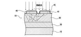
- FIG. 1 is a schematic diagram showing an outline of the configuration of an example of the Raman scattered light enhancing element of the present invention.
- the Raman scattered light enhancing element 10 according to this embodiment is formed, for example, on a flat substrate 15, a high reflection layer 20 formed on the surface of the substrate 15, and a surface of the high reflection layer 20. It has a multilayer structure including a dielectric layer 30 and an enhanced electromagnetic field forming layer 40 made of a large number of silver fine particles 41 formed on the surface of the dielectric layer 30, and a gold layer is formed on the surface of the enhanced electromagnetic field forming layer 40.
- a film 45 is formed.
- the Raman scattered light enhancing element 10 excites, for example, an analyte (Raman active chemical species) carried directly or via a spacer on the surface of a region located on the surface of the silver fine particles 41 in the gold film 45. This enhances Raman scattered light by light irradiation.
- substrate 15 is not specifically limited, For example, glass, ceramics, resin, a metal etc. can be illustrated. As will be described later, when heat treatment (for example, heating at 200 ° C. or higher) is performed in the manufacturing process of the Raman scattered light enhancing element 10, it is preferable to have heat resistance such as glass or polyimide resin. Further, the surface of the substrate 15 on the high reflection layer 20 side does not have to be a flat surface, and may be a curved surface, a small spherical surface, or the like, for example.
- the highly reflective layer 20 is preferably made of a material having high reflectivity, for example, in the entire visible region or in a wavelength region of at least 500 nm or more, specifically, in the wavelength region of excitation light that excites the analyte. Specifically, for example, silver, gold, aluminum, or copper can be exemplified.
- the thickness of the highly reflective layer 20 is preferably large enough to obtain a reflectance of 90% or more in the entire visible region or in a wavelength region of 500 nm or more.
- the surface of the highly reflective layer 20 on the dielectric layer 30 side may be an optically smooth surface, but is preferably a rough surface. Specifically, for example, a rough surface having a surface roughness Ra of about 10 to 30 nm is preferable. Thereby, as shown in the result of the experimental example to be described later, a higher light enhancement effect can be obtained.
- the dielectric layer 30 is made of a material that is transparent to excitation light. As will be described later, heat treatment (for example, heating at 200 ° C. or higher) is performed in the manufacturing process of the Raman scattered light enhancing element 10. In that case, it is preferably made of a material having heat resistance. Specific examples include SOG (spin-on-glass) materials mainly composed of silicon oxide, siloxane-based materials such as tetraethoxysilane (TEOS) and dimethylsiloxane. Further, when the dielectric layer 30 is composed of a fired body (SOG film) obtained by firing an SOG material, the surface of the SOG film has a relatively strong hydrophobicity, so that an alkali treatment is performed as necessary.
- SOG spin-on-glass
- the enhanced electromagnetic field forming layer 40 is preferably composed of a single layer film composed of a large number of silver fine particles 41.
- the silver fine particles 41 have a size equal to or smaller than the wavelength of the excitation light, for example, a cross-sectional particle size (a horizontal dimension in FIG. 1) d of 30 to 400 nm and a thickness t of 5 to 70 nm. Those having shape anisotropy such as a shape can be preferably used.
- the silver fine particles 41 having the above-mentioned size are, for example, two-dimensionally randomly, specifically, for example, a density of 10 8 to 10 10 particles / cm 2 . And are arranged in an independent state without contacting each other. Further, the enhanced electromagnetic field forming layer 40 may be configured such that the silver fine particles 41 are regularly arranged.
- a method for forming such an enhanced electromagnetic field forming layer 40 is not particularly limited.
- a method in which a dispersion in which silver fine particles are dispersed in an appropriate solvent is applied by a spin coating method and heated, dipping Then, a heating method, a vacuum deposition method, or the like can be suitably used.
- the gold film 45 is formed on the entire surface of the enhanced electromagnetic field forming layer 40, but at least the outer surface of the silver fine particles 41 (excitation light is generated). What is necessary is just to be formed on the surface to be irradiated.
- an enhanced electromagnetic field forming layer may be formed by composite metal fine particles having a core-shell structure in which the surface of silver fine particles (core particles) is coated with a coating made of gold.
- the thickness of the gold film 45 is preferably 4 to 10% of the thickness t of the silver fine particles 41, for example.
- the thickness of the gold film 45 is preferably 2 to 5 nm.
- Such a gold film 45 can be formed by sputtering, for example.
- the object to be analyzed is directly or on the surface of the region located on the surface of the silver fine particles 41 in the gold film 45.
- a Raman signal with a high S / N ratio is obtained, it is desirable that the analysis object is directly supported on the surface of the gold film 45.
- the Raman scattered light emitted when an analysis object is excited by irradiation of excitation light is detected by an appropriate spectrometer.
- the spacer is for adjusting the distance between the surface of the gold film 45 and the object to be analyzed, and can be composed of a dielectric such as an SOG film.
- the thickness of the spacer is preferably, for example, 10 nm or less, and the Raman light enhancement effect is maximized particularly when it is 1 nm or less.
- the Raman scattered light enhancing element 10 basically has a multilayer structure in which the highly reflective layer 20, the dielectric layer 30, and the enhanced electromagnetic field forming layer 40 are formed on the substrate 15.
- a strong enhanced electromagnetic field can be formed in the vicinity of each silver fine particle 41 constituting the enhanced electromagnetic field forming layer 40. Therefore, as is clear from the results of the experimental examples described later, the Raman scattered light enhancement is sufficiently high. An effect is obtained. The reason for this is that, as shown in FIG. 2, interference in which positive interference occurs between the excitation light and the reflected light of the excitation light by the high reflection layer 20 in the vicinity of each silver fine particle 41 constituting the enhanced electromagnetic field forming layer 40.
- a field is formed, and it is considered that the enhanced electromagnetic field (region surrounded by a broken line in FIG. 2) due to the localized surface plasmon of the silver fine particles 41 is further enhanced by the action of the interference field.
- the well-known interference effect alone cannot sufficiently explain the large Raman enhancement factor shown in the experimental example, and the secondary electromagnetic field itself radiated by the localized surface plasmons of the silver fine particles 41 is the highly reflective layer. It is presumed that the presence of 20 causes a high-order enhancement such as self-amplification, thereby generating a large enhanced electromagnetic field that cannot be imagined from conventional common sense.
- an extremely low output and small light source such as an LD (semiconductor laser) or LED (light emitting diode) is used as the excitation light source
- an expected Raman signal can be obtained with certainty.
- the Raman spectrum of the Raman active chemical species can be measured.
- the desired Raman spectroscopic analysis can be performed with a very simple structure such as the measurement system used in the experimental example.
- the Raman scattered light enhancing element 10 reduces the background noise (fluorescence signal) due to the fluorescence quenching action of the gold film 45 by using the analyte to be carried on the surface of the gold film 45. And a Raman signal with a high S / N ratio can be obtained.
- gold is excellent in chemical stability, for example, if the structure does not have a gold film, the analysis object undergoes a chemical change (analysis object and silver form a compound). Therefore, there is no problem that the analysis result may be difficult to interpret, and for this reason, the Raman signal can be reliably detected.
- the gold film 45 is formed on the entire surface of the enhanced electromagnetic field forming layer 40, the silver fine particles 41 can be prevented from falling off, so that the expected function can be stably expressed. Will be.
- the silver fine particles 41 have shape anisotropy and uniform particle diameters, and the gold film 45 is formed on the outer surface of the silver fine particles 41. Since the wavelength characteristic (resonance wavelength) can be adjusted by adjusting the film thickness of the gold film 45 in accordance with the thickness (height), an expected Raman scattered light enhancement effect can be obtained in a wide wavelength range. it can.
- the enhanced electromagnetic field forming layer itself does not have to have a structure (nanostructure) in which the light enhancement effect by the localized surface plasmon is dominant (dominant).
- the structure itself is simplified by eliminating the structural constraints of conventional light-enhancing elements using the mechanism based on the interaction between the localized surface plasmons of fine particles and the surface plasmon polaritons between the metal fine particles and the highly reflective layer. It is easy to handle and can be produced advantageously in terms of cost.
- a solution obtained by appropriately diluting a commercially available dimethylsiloxane solution with ethanol is spin-coated on the roughened surface (upper surface) of the silver film at 3000 rpm, and then heated on a hot plate at 200 to 250 ° C. for several minutes.
- a dielectric film (refractive index: 1.3 to 1.4) as a dielectric layer (30) was formed.
- the thickness of the dielectric film is about 80 nm.
- the hydrophilization process by a plasma process was performed with respect to the surface (upper surface) of the obtained dielectric film.
- an acetone dispersion liquid (concentration of about 0.4 wt%) of protective film-free silver nanoparticles (volume average particle diameter of about 15 nm) is spin-coated at 3000 revolutions on the hydrophilic surface (upper surface) of the dielectric film, Thereafter, the resultant was heated on a hot plate at about 250 ° C. for several minutes to form a silver ultrafine particle single layer film as an enhanced electromagnetic field forming layer (40).
- the cross-sectional particle size (d) of the ultrafine silver particles is about 150 nm on average
- the thickness (t) is about 30 nm on average
- a density of 10 8 to 10 10 particles / cm 2 is about 150 nm on average
- each silver ultrafine particle has high crystallinity similar to bulk silver.
- a gold film (45) was formed on the surface of the silver ultrafine particle single layer film by the sputtering method under the following conditions.
- reference numeral 50 denotes a He—Ne laser (wavelength 632.8 nm) used as an excitation light source and having an output of less than 1 mW, and is not condensed (energy density is about 300 mW / mm) through a filter (not shown).
- cm 2 ) or anti-condensing is applied to the Raman scattered light enhancing element 10 as excitation light.
- the Raman scattered light enhancing element 10 is rotatably provided, and the incident angle of the excitation light can be set.
- the excitation light is incident on the Raman scattered light enhancing element 10 at an incident angle of 45 °, and is scattered in the 90 ° angular direction by the dye supported by the Raman scattered light enhancing element 10.
- a condensing lens (aperture 35 mm) 53 disposed at a position approximately 13 cm away from the surface of the Raman scattered light enhancing element 10 is used to pass Raman scattered light through a filter 54 to a light receiving head 56 of an electronic cooling diode array detector 55. Condensed.
- the Raman scattered light enhancing element according to the present invention, the level (absolute value) of the detected signal is reduced as compared with the comparative Raman scattered light enhancing element. It was confirmed that a Raman signal with a high S / N ratio was obtained.
- the maximum film thickness obtained is 180 nm, and when forming a dielectric film with a large film thickness, the above treatment was repeated a plurality of times. .
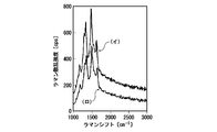
- Raman scattering has a structure in which the surface of the silver film (highly reflective layer) on the dielectric film side is made rough so that the surface of the silver film is optically smooth. It was confirmed that the Raman scattering intensity (Raman signal) was higher than that of the light enhancement element, and a higher enhancement effect was obtained.
Landscapes
- Physics & Mathematics (AREA)
- Health & Medical Sciences (AREA)
- General Physics & Mathematics (AREA)
- Biochemistry (AREA)
- Chemical & Material Sciences (AREA)
- Analytical Chemistry (AREA)
- Life Sciences & Earth Sciences (AREA)
- General Health & Medical Sciences (AREA)
- Nuclear Medicine, Radiotherapy & Molecular Imaging (AREA)
- Immunology (AREA)
- Pathology (AREA)
- Optics & Photonics (AREA)
- Investigating, Analyzing Materials By Fluorescence Or Luminescence (AREA)
Abstract
Description
近年においては、金属ナノ粒子の局在型表面プラズモンを利用して、金属ナノ粒子の表面に吸着させた分析対象物にレーザー光を照射し、これにより発生するラマン散乱光を飛躍的に増強させて検出する表面増強ラマン散乱(SERS)の研究が進められている。
そして、この光センサによれば、銀ナノ粒子の局在型表面プラズモンと平滑な銀膜の表面プラズモンポラリトンモードの共鳴によって発現する増強電磁場の作用により、ラマン信号の高次の増強効果が得られ、さらに、金属ナノ粒子層に規則的な周期構造をもうけることによって、一層強い増強効果が得られる、とされている。
しかしながら、ラマン信号の測定感度は、上記のような増強ラマン散乱法によって、ある程度のレベルまで向上しているものの、高出力のレーザー光源を必須とし、また、その他の光学素子(顕微鏡も含む)、液体窒素冷却型高感度検出器などが必要とされることも含め、極めて高額な分析機器であると言わざるをえない。すなわち、特許文献1には、例えば0.4μW程度の非常に小さなレーザー光のパワーでラマン信号(SERS信号)が得られること(増強率にして最大1014倍)が記載されているが、分析感度の評価は、励起レーザー光のパワーそのものではなく、照射パワー密度の大小で比較することが必要とされる。従って、上記のレーザー光源は、照射面積あたりの励起パワー密度は約13,000mW/cm2 もの大きな値になる、高出力のものが必要とされることとなる。
以上のように、上記の要請を満足するラマン分析装置は、知られていないのが実情である。
前記増強電磁場形成層を構成する銀微粒子の表面に、金膜が形成されていることを特徴とする。
さらにまた、金は化学的安定性に優れたものであるので、例えば金膜を有さない構成のものであれば、分析対象物が化学変化(分析対象物と銀とが化合物を形成)を起こして分析結果の解釈に困ることがあるといった問題が生ずることがなく、この理由によっても、ラマン信号を確実に検出することができるようになる。
さらにまた、増強電磁場形成層の表面の全面に金膜が形成された構成とされていることにより、銀微粒子の脱落を防止することができるので、所期の機能が安定して発現されるものとなる。
図1は、本発明のラマン散乱光増強素子の一例に構成の概略を示す模式図である。
この実施の形態に係るラマン散乱光増強素子10は、例えば平板状の基板15と、この基板15の表面上に形成された高反射層20と、この高反射層20の表面上に形成された誘電体層30と、この誘電体層30の表面上に形成された、多数の銀微粒子41による増強電磁場形成層40とを含む多層構造を有し、増強電磁場形成層40の表面上に、金膜45が形成されている。このラマン散乱光増強素子10は、例えば、金膜45における銀微粒子41の表面上に位置された領域の表面上に直接あるいはスペーサーを介して担持させた分析対象物(ラマン活性化学種)に対する励起光照射によるラマン散乱光を増強させるものである。
また、基板15の高反射層20側の表面は、平面である必要はなく、例えば曲面、小球面などとされていてもよい。
高反射層20の厚みは、可視領域全域または500nm以上の波長領域で90%以上の反射率が得られる大きさであることが好ましい。
また、高反射層20における誘電体層30側の表面は、光学的に平滑な面であってもよいが、粗面とされていることが好ましい。具体的には例えば、表面粗さRaが10~30nm程度である荒れた面であることが好ましい。これにより、後述する実験例の結果に示されているように、一層高い光増強効果が得られる。
誘電体層30の厚みは、光学的距離nd=50nm以上であることが好ましく、より好ましくは60~90nmとされる。誘電体層30の厚みが過小である場合には、後述する実験例の結果に示されるように、十分な光増強効果を得ることができない。
銀微粒子41は、励起光の波長以下の大きさ、例えば断面粒径(図1における左右方向の寸法)dが30~400nm、厚さtが5~70nmである、例えば扁平な球形状、平板状の形状など、形状異方性を有するものを好適に用いることができる。ここに、銀微粒子41は、いずれも均一の大きさ及び形状を備えていることが望ましいが、大きさや形状に多少のばらつきがあってもよい。
また、増強電磁場形成層40は、銀微粒子41が規則的に配列されてなる構成とされていてもよい。
金膜45の厚さは、銀微粒子41の厚さtの例えば4~10%の大きさとされていることが好ましい。具体的には例えば、銀微粒子41の大きさが上記数値範囲である場合には、金膜45の厚さは、2~5nmであることが好ましい。
このような金膜45は、例えばスパッタリング法により形成することができる。
そして、励起光の照射によって分析対象物が励起されて発せられるラマン散乱光が適宜の分光器によって検出される。
スペーサーの厚みは、例えば10nm以下であることが好ましく、特に1nm以下である場合に、ラマン光増強効果が最大となる。
しかも、励起用光源として、例えばLD(半導体レーザー)やLED(発光ダイオード)といった、きわめて低出力かつ小型の光源を用いた場合であっても、所期のラマン信号を確実に得ることができる。具体的には例えば、エネルギー密度が10mW/cm2 以下である低出力のレーザー光を励起光として用いた場合であっても、ラマン活性化学種のラマンスペクトルを測定することができ、従って、後述する実験例において用いた測定システムのような極めて簡単な構造で、所望のラマン分光分析を行うことができる。
さらにまた、金は化学的安定性に優れたものであるので、例えば金膜を有さない構成のものであれば、分析対象物が化学変化(分析対象物と銀とが化合物を形成)を起こして分析結果の解釈に困ることがあるといった問題が生ずることがなく、この理由によっても、ラマン信号を確実に検出することができるようになる。
さらにまた、増強電磁場形成層40の表面の全面に金膜45が形成された構成とされていることにより、銀微粒子41の脱落を防止することができるので、所期の機能が安定して発現されるものとなる。
〔ラマン散乱光増強素子(10)の作製〕
基板(15)として1cm角の大きさのスライドガラスを用い、このスライドガラスの表面上に、標準的な抵抗加熱型真空蒸着法により高反射層(20)としての銀膜を形成した。得られた銀膜の厚さは0.2μm以上で透過率は可視領域で実質的にゼロであった。また実測反射率は、可視領域のほぼ全域で98%以上の、バルク銀の光学定数を用いて理論的に計算した値と一致する、高い反射率を示すことがわかった。
次いで、市販のジメチルシロキサン溶液をエタノールで適宜希釈した溶液を銀膜の粗面化された表面(上面)上に3000回転でスピンコートし、その後200~250℃のホットプレート上で数分間加熱処理することにより誘電体層(30)としての誘電体膜(屈折率1.3~1.4)を形成した。誘電体膜の厚さは、約80nmである。そして、得られた誘電体膜の表面(上面)に対して、プラズマ処理による親水化処理を行った。
次いで、保護膜フリー銀ナノ粒子(体積平均粒径約15nm)のアセトン分散液(濃度約0.4wt%)を誘電体膜の親水化処理した表面(上面)上に3000回転でスピンコートし、その後約250℃のホットプレート上で数分間加熱することにより、増強電磁場形成層(40)としての銀超微粒子単層膜を形成した。得られた銀超微粒子単層膜における銀超微粒子の断面粒径(d)は平均で約150nm、厚さ(t)は平均で約30nmであり、108 ~1010個/cm2 の密度で分布した状態で二次元的にランダムに配列されてなる。また、各銀超微粒子は、XRD(X線回折)測定によりバルク銀なみの高い結晶性を有することが確認された。
そして、銀超微粒子単層膜の表面に、スパッタリング法により以下に示す条件で、金膜(45)を形成した。
ION SPUTTER装置「JFC-1100」(日本電子社製)を用い、基板を、ターゲットから誘電体膜の表面までの離間距離が40mmとなる状態で、設置した。雰囲気はAr:0.15Torrであり、放電電流は7~8mA、ターゲット電圧は-0.7kV、時間は1~2分間である。
上記のラマン散乱光増強素子の作製工程において、銀超微粒子単層膜の表面に金膜を形成しないことの他は、上記と同様の方法により、金膜を有さないことの他は、上記のラマン散乱光増強素子と同一の構成を有する比較用のラマン散乱光増強素子を作製した。
ローダミン6G(Rh6G)色素の希薄エタノール溶液を、ラマン散乱光増強素子における金膜の表面上に3000回転でスピンコートすることにより、色素分子を金膜の表面上に担持させた。ここに、ラマン散乱光増強素子の表面に担持される色素分子の密度とスピンコートに用いた溶液の色素濃度との関係は、ローダミン6Gの濃度が0.3mMである場合に、色素分子の密度は7×10¹³個/cm2 である。比較用のラマン散乱光増強素子においては、同様の方法により、色素分子を銀超微粒子単層膜の表面上に担持させた。
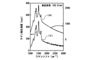
上記のようにして作製したラマン散乱光増強素子および比較用のラマン散乱光増強素子の各々について、励起光照射により試料(色素分子)から発せられるラマン散乱光を図3に示す構成の測定システムにより測定した。結果を図4に示す。図4において、曲線(イ)が本発明に係るラマン散乱光増強素子(金膜を具備)によるものであり、曲線(ロ)が比較用のラマン散乱光増強素子によるものである。
図3において、符号50は、励起用光源として用いた、出力1mW未満のHe-Neレーザー(波長632.8nm)であり、フィルタ(図示せず)を介して非集光(エネルギー密度約300mW/cm2 )もしくは反集光(デフォーカスされた,エネルギー密度約10mW/cm2 以下)励起光としてラマン散乱光増強素子10に照射する。この測定システムにおいて、ラマン散乱光増強素子10は回転自在に設けており、励起光の入射角度を設定可能に構成した。ラマン散乱光の測定においては、励起光をラマン散乱光増強素子10に対して45°の入射角度で入射させ、ラマン散乱光増強素子10によって担持された色素による90°の角度方向に散乱されるラマン散乱光を、ラマン散乱光増強素子10の表面から約13cm離れた位置に配置した集光レンズ(口径35mm)53によって、電子冷却型ダイオードアレイ検出器55の受光ヘッド56にフィルタ54を介して集光した。
実験例1において作製したラマン散乱光増強素子において、誘電体層の厚みが下記表1に従って調整された6つのラマン散乱光増強素子を、実験例1において作製したものと同様の方法により作製し、実験例1と同様の方法により、ラマン散乱光(ラマン散乱強度)の測定を行った。結果を下記表1に示す。
ここに、誘電体膜の厚みは、AFMによる段差測定により実測した、スピンコートに用いた溶液濃度と形成する透明誘電体膜の厚さの関係(検量線)に基づいて適宜調整した。ここに、市販のジメチルシロキサン溶液の原液をそのままスピンコートした場合に得られる最大膜厚は180nmであり、大きな膜厚の誘電体膜を形成する際には、上記の処理を複数回繰り返し行った。

実験例1におけるラマン散乱光増強素子の作製工程において、銀膜(高反射層)における誘電体膜側の表面に対して加熱処理による粗面化処理を行い当該表面を光学的に粗面としたことの他は、上記と同様の方法により、実験例1に係るラマン散乱光増強素子と同一の構成を有するラマン散乱光増強素子を作製した。ここに、銀膜の表面の表面粗さRaは、AFM測定により、10~30nm程度であった。
そして、実験例1と同様の方法により、ラマン散乱光(ラマン散乱強度)の測定を行った。結果を図5に示す。図5において、曲線(イ)が高反射層の表面が粗面とされた光増強素子によるものであり、曲線(ロ)が高反射層の表面が光学的に平滑面とされた光増強素子(実験例1において作製したもの)によるものである。
15 基板
20 高反射層
30 誘電体層
40 増強電磁場形成層
41 銀微粒子
45 金膜
50 He-Neレーザー
53 集光レンズ
54 フィルタ
55 電子冷却型ダイオードアレイ検出器
56 受光ヘッド
Claims (8)
- 基板と、この基板上に形成された高反射層と、この高反射層上に形成された誘電体層と、この誘電体層上に形成された、多数の銀微粒子による増強電磁場形成層とよりなり、
前記増強電磁場形成層を構成する銀微粒子の表面に、金膜が形成されていることを特徴とするラマン散乱光増強素子。 - 前記誘電体層は、厚みが光学的距離nd=50nm以上であることを特徴とする請求項1に記載のラマン散乱光増強素子。
- 前記金膜が、前記増強電磁場形成層の表面の全面に形成されていることを特徴とする請求項1または請求項2に記載のラマン散乱光増強素子。
- 前記高反射層は、銀、金、アルミニウム、銅のうちから選ばれた金属により構成されることを特徴とする請求項1乃至請求項3のいずれかに記載のラマン散乱光増強素子。
- 前記高反射層における誘電体層側の表面が粗面とされていることを特徴とする請求項1乃至請求項4のいずれかに記載のラマン散乱光増強素子。
- 前記粗面は、表面粗さがRa=10~30nmであることを特徴とする請求項5に記載のラマン散乱光増強素子。
- 前記増強電磁場形成層は、銀微粒子がランダムに配列されてなることを特徴とする請求項1乃至請求項5のいずれかに記載のラマン散乱光増強素子。
- 前記銀微粒子は、108 ~1010個/cm2 の密度で分布し、互いに接触することなく独立した状態でランダムに配列されていることを特徴とする請求項7に記載のラマン散乱光増強素子。
Priority Applications (2)
| Application Number | Priority Date | Filing Date | Title |
|---|---|---|---|
| US13/996,456 US20130271841A1 (en) | 2010-12-22 | 2011-12-19 | Raman scattering light enhancing device |
| JP2012549795A JPWO2012086586A1 (ja) | 2010-12-22 | 2011-12-19 | ラマン散乱光増強素子 |
Applications Claiming Priority (2)
| Application Number | Priority Date | Filing Date | Title |
|---|---|---|---|
| JP2010285637 | 2010-12-22 | ||
| JP2010-285637 | 2010-12-22 |
Publications (1)
| Publication Number | Publication Date |
|---|---|
| WO2012086586A1 true WO2012086586A1 (ja) | 2012-06-28 |
Family
ID=46313856
Family Applications (1)
| Application Number | Title | Priority Date | Filing Date |
|---|---|---|---|
| PCT/JP2011/079360 Ceased WO2012086586A1 (ja) | 2010-12-22 | 2011-12-19 | ラマン散乱光増強素子 |
Country Status (3)
| Country | Link |
|---|---|
| US (1) | US20130271841A1 (ja) |
| JP (1) | JPWO2012086586A1 (ja) |
| WO (1) | WO2012086586A1 (ja) |
Cited By (9)
| Publication number | Priority date | Publication date | Assignee | Title |
|---|---|---|---|---|
| JP2013195204A (ja) * | 2012-03-19 | 2013-09-30 | Seiko Epson Corp | 試料分析基板および検出装置 |
| JP2014190910A (ja) * | 2013-03-28 | 2014-10-06 | Seiko Epson Corp | センサー基板、検出装置及び電子機器 |
| WO2014188622A1 (ja) * | 2013-05-20 | 2014-11-27 | ウシオ電機株式会社 | 検査方法 |
| WO2014188621A1 (ja) * | 2013-05-20 | 2014-11-27 | ウシオ電機株式会社 | 検査方法、センサ |
| WO2014188620A1 (ja) * | 2013-05-20 | 2014-11-27 | ウシオ電機株式会社 | センサ、検査方法 |
| CN104422682A (zh) * | 2013-09-05 | 2015-03-18 | 精工爱普生株式会社 | 拉曼分光装置、拉曼分光法以及电子设备 |
| JP2017156104A (ja) * | 2016-02-29 | 2017-09-07 | 西松建設株式会社 | 光増強素子とその製造方法ならびに分光分析用キットおよび分光分析方法 |
| JP2017173336A (ja) * | 2017-05-22 | 2017-09-28 | セイコーエプソン株式会社 | センサー基板、検出装置及び電子機器 |
| JP2017211395A (ja) * | 2017-09-08 | 2017-11-30 | セイコーエプソン株式会社 | ラマン分光装置、ラマン分光法、および電子機器 |
Families Citing this family (1)
| Publication number | Priority date | Publication date | Assignee | Title |
|---|---|---|---|---|
| CN113699481A (zh) * | 2021-08-25 | 2021-11-26 | 山东智微检测科技有限公司 | 负载金银纳米膜的复合结构阵列及其制备方法和应用 |
Citations (5)
| Publication number | Priority date | Publication date | Assignee | Title |
|---|---|---|---|---|
| JP2003511666A (ja) * | 1999-10-06 | 2003-03-25 | サーロメッド・インコーポレーテッド | 新規な表面強化されたラマン散乱(sers)−活性基体及びラマン分光とキャピラリー電気泳動(ce)を接続する方法 |
| WO2005095927A1 (ja) * | 2004-03-31 | 2005-10-13 | Omron Corporation | 局在プラズモン共鳴センサ及び検査装置 |
| JP2007139540A (ja) * | 2005-11-17 | 2007-06-07 | Kyoto Univ | 蛍光増強素子、蛍光素子、及び蛍光増強方法 |
| JP2007538264A (ja) * | 2004-05-19 | 2007-12-27 | ブィピー ホールディング、エルエルシー | Sersによる化学基の増強検出のための層状プラズモン構造をもつ光センサ |
| JP2008014933A (ja) * | 2006-06-08 | 2008-01-24 | Fujifilm Corp | ラマン分光用デバイス、及びラマン分光装置 |
-
2011
- 2011-12-19 JP JP2012549795A patent/JPWO2012086586A1/ja active Pending
- 2011-12-19 US US13/996,456 patent/US20130271841A1/en not_active Abandoned
- 2011-12-19 WO PCT/JP2011/079360 patent/WO2012086586A1/ja not_active Ceased
Patent Citations (5)
| Publication number | Priority date | Publication date | Assignee | Title |
|---|---|---|---|---|
| JP2003511666A (ja) * | 1999-10-06 | 2003-03-25 | サーロメッド・インコーポレーテッド | 新規な表面強化されたラマン散乱(sers)−活性基体及びラマン分光とキャピラリー電気泳動(ce)を接続する方法 |
| WO2005095927A1 (ja) * | 2004-03-31 | 2005-10-13 | Omron Corporation | 局在プラズモン共鳴センサ及び検査装置 |
| JP2007538264A (ja) * | 2004-05-19 | 2007-12-27 | ブィピー ホールディング、エルエルシー | Sersによる化学基の増強検出のための層状プラズモン構造をもつ光センサ |
| JP2007139540A (ja) * | 2005-11-17 | 2007-06-07 | Kyoto Univ | 蛍光増強素子、蛍光素子、及び蛍光増強方法 |
| JP2008014933A (ja) * | 2006-06-08 | 2008-01-24 | Fujifilm Corp | ラマン分光用デバイス、及びラマン分光装置 |
Non-Patent Citations (1)
| Title |
|---|
| MITSUO KAWASAKI: "Kinzoku Nano Ryushi - Nano Kozo Usumaku no Hyomen Plasmon Kyomei ga Motarasu Shin Gensho -Shikiso no Zokyo Hikari Kyushu. Zokyo Hakko o Chushin to shite", THE JOURNAL OF THE SOCIETY OF SCIENTIFIC PHOTOGRAPHY OF JAPAN, vol. 73, no. 6, 25 December 2010 (2010-12-25), pages 308 - 309 * |
Cited By (11)
| Publication number | Priority date | Publication date | Assignee | Title |
|---|---|---|---|---|
| JP2013195204A (ja) * | 2012-03-19 | 2013-09-30 | Seiko Epson Corp | 試料分析基板および検出装置 |
| JP2014190910A (ja) * | 2013-03-28 | 2014-10-06 | Seiko Epson Corp | センサー基板、検出装置及び電子機器 |
| WO2014188622A1 (ja) * | 2013-05-20 | 2014-11-27 | ウシオ電機株式会社 | 検査方法 |
| WO2014188621A1 (ja) * | 2013-05-20 | 2014-11-27 | ウシオ電機株式会社 | 検査方法、センサ |
| WO2014188620A1 (ja) * | 2013-05-20 | 2014-11-27 | ウシオ電機株式会社 | センサ、検査方法 |
| CN104422682A (zh) * | 2013-09-05 | 2015-03-18 | 精工爱普生株式会社 | 拉曼分光装置、拉曼分光法以及电子设备 |
| JP2015052463A (ja) * | 2013-09-05 | 2015-03-19 | セイコーエプソン株式会社 | ラマン分光装置、ラマン分光法、および電子機器 |
| CN104422682B (zh) * | 2013-09-05 | 2019-04-19 | 精工爱普生株式会社 | 拉曼分光装置、拉曼分光法以及电子设备 |
| JP2017156104A (ja) * | 2016-02-29 | 2017-09-07 | 西松建設株式会社 | 光増強素子とその製造方法ならびに分光分析用キットおよび分光分析方法 |
| JP2017173336A (ja) * | 2017-05-22 | 2017-09-28 | セイコーエプソン株式会社 | センサー基板、検出装置及び電子機器 |
| JP2017211395A (ja) * | 2017-09-08 | 2017-11-30 | セイコーエプソン株式会社 | ラマン分光装置、ラマン分光法、および電子機器 |
Also Published As
| Publication number | Publication date |
|---|---|
| JPWO2012086586A1 (ja) | 2014-05-22 |
| US20130271841A1 (en) | 2013-10-17 |
Similar Documents
| Publication | Publication Date | Title |
|---|---|---|
| JPWO2012086586A1 (ja) | ラマン散乱光増強素子 | |
| JP2012132804A (ja) | 光増強素子 | |
| US8358407B2 (en) | Enhancing signals in Surface Enhanced Raman Spectroscopy (SERS) | |
| Bonyár et al. | Investigation of the performance of thermally generated gold nanoislands for LSPR and SERS applications | |
| Félidj et al. | Gold particle interaction in regular arrays probed by surface enhanced Raman scattering | |
| Lay et al. | Aluminum nanostructures with strong visible-range SERS activity for versatile micropatterning of molecular security labels | |
| CN101688809B (zh) | 电场增强结构及使用其的检测装置 | |
| US8837039B2 (en) | Multiscale light amplification structures for surface enhanced Raman spectroscopy | |
| CN111356943A (zh) | 场增强装置 | |
| JP2007538264A (ja) | Sersによる化学基の増強検出のための層状プラズモン構造をもつ光センサ | |
| US20140242573A1 (en) | Optical element, analysis device, analysis method and electronic apparatus | |
| US20140242571A1 (en) | Optical element, analysis equipment, analysis method and electronic apparatus | |
| Cade et al. | The plasmonic engineering of metal nanoparticles for enhanced fluorescence and Raman scattering | |
| D’Andrea et al. | Red shifted spectral dependence of the SERS enhancement in a random array of gold nanoparticles covered with a silica shell: extinction versus scattering | |
| WO2012132385A1 (ja) | 光電場増強デバイスの製造方法 | |
| JP2010532464A (ja) | 誘電体粒子を含む電界増強構造とその電界増強構造を含む装置及びその使用方法 | |
| Li et al. | Multilayer enhanced gold film over nanostructure surface-enhanced Raman substrates | |
| JP7598614B2 (ja) | ラマン分光測定装置、ラマン分光測定方法および表面増強ラマン散乱デバイス | |
| Rubish et al. | Rapid formation methods of arrays of randomly distributed Au and Ag nanoparticles, their morphologies and optical characteristics | |
| JP5884527B2 (ja) | 光増強素子およびその作製方法 | |
| JP6337127B2 (ja) | 光電場増強デバイスおよび光電場増強デバイスの製造方法 | |
| US7474397B2 (en) | Raman and hyper-Raman excitation using superlensing | |
| JP2014211326A (ja) | ラマンセンサー | |
| RU2696899C1 (ru) | Устройство усиления комбинационного рассеяния света | |
| TWI750718B (zh) | 增強訊號之結構及其製作方法 |
Legal Events
| Date | Code | Title | Description |
|---|---|---|---|
| 121 | Ep: the epo has been informed by wipo that ep was designated in this application |
Ref document number: 11849935 Country of ref document: EP Kind code of ref document: A1 |
|
| DPE1 | Request for preliminary examination filed after expiration of 19th month from priority date (pct application filed from 20040101) | ||
| ENP | Entry into the national phase |
Ref document number: 2012549795 Country of ref document: JP Kind code of ref document: A |
|
| WWE | Wipo information: entry into national phase |
Ref document number: 13996456 Country of ref document: US |
|
| NENP | Non-entry into the national phase |
Ref country code: DE |
|
| 122 | Ep: pct application non-entry in european phase |
Ref document number: 11849935 Country of ref document: EP Kind code of ref document: A1 |