WO2012086480A1 - 蒸着装置、蒸着方法、並びに、有機エレクトロルミネッセンス表示装置の製造方法 - Google Patents
蒸着装置、蒸着方法、並びに、有機エレクトロルミネッセンス表示装置の製造方法 Download PDFInfo
- Publication number
- WO2012086480A1 WO2012086480A1 PCT/JP2011/078861 JP2011078861W WO2012086480A1 WO 2012086480 A1 WO2012086480 A1 WO 2012086480A1 JP 2011078861 W JP2011078861 W JP 2011078861W WO 2012086480 A1 WO2012086480 A1 WO 2012086480A1
- Authority
- WO
- WIPO (PCT)
- Prior art keywords
- vapor deposition
- deposition source
- injection
- particles
- substrate
- Prior art date
- Legal status (The legal status is an assumption and is not a legal conclusion. Google has not performed a legal analysis and makes no representation as to the accuracy of the status listed.)
- Ceased
Links
Images







Classifications
-
- C—CHEMISTRY; METALLURGY
- C23—COATING METALLIC MATERIAL; COATING MATERIAL WITH METALLIC MATERIAL; CHEMICAL SURFACE TREATMENT; DIFFUSION TREATMENT OF METALLIC MATERIAL; COATING BY VACUUM EVAPORATION, BY SPUTTERING, BY ION IMPLANTATION OR BY CHEMICAL VAPOUR DEPOSITION, IN GENERAL; INHIBITING CORROSION OF METALLIC MATERIAL OR INCRUSTATION IN GENERAL
- C23C—COATING METALLIC MATERIAL; COATING MATERIAL WITH METALLIC MATERIAL; SURFACE TREATMENT OF METALLIC MATERIAL BY DIFFUSION INTO THE SURFACE, BY CHEMICAL CONVERSION OR SUBSTITUTION; COATING BY VACUUM EVAPORATION, BY SPUTTERING, BY ION IMPLANTATION OR BY CHEMICAL VAPOUR DEPOSITION, IN GENERAL
- C23C14/00—Coating by vacuum evaporation, by sputtering or by ion implantation of the coating forming material
- C23C14/06—Coating by vacuum evaporation, by sputtering or by ion implantation of the coating forming material characterised by the coating material
- C23C14/12—Organic material
-
- C—CHEMISTRY; METALLURGY
- C23—COATING METALLIC MATERIAL; COATING MATERIAL WITH METALLIC MATERIAL; CHEMICAL SURFACE TREATMENT; DIFFUSION TREATMENT OF METALLIC MATERIAL; COATING BY VACUUM EVAPORATION, BY SPUTTERING, BY ION IMPLANTATION OR BY CHEMICAL VAPOUR DEPOSITION, IN GENERAL; INHIBITING CORROSION OF METALLIC MATERIAL OR INCRUSTATION IN GENERAL
- C23C—COATING METALLIC MATERIAL; COATING MATERIAL WITH METALLIC MATERIAL; SURFACE TREATMENT OF METALLIC MATERIAL BY DIFFUSION INTO THE SURFACE, BY CHEMICAL CONVERSION OR SUBSTITUTION; COATING BY VACUUM EVAPORATION, BY SPUTTERING, BY ION IMPLANTATION OR BY CHEMICAL VAPOUR DEPOSITION, IN GENERAL
- C23C14/00—Coating by vacuum evaporation, by sputtering or by ion implantation of the coating forming material
- C23C14/22—Coating by vacuum evaporation, by sputtering or by ion implantation of the coating forming material characterised by the process of coating
- C23C14/24—Vacuum evaporation
-
- C—CHEMISTRY; METALLURGY
- C23—COATING METALLIC MATERIAL; COATING MATERIAL WITH METALLIC MATERIAL; CHEMICAL SURFACE TREATMENT; DIFFUSION TREATMENT OF METALLIC MATERIAL; COATING BY VACUUM EVAPORATION, BY SPUTTERING, BY ION IMPLANTATION OR BY CHEMICAL VAPOUR DEPOSITION, IN GENERAL; INHIBITING CORROSION OF METALLIC MATERIAL OR INCRUSTATION IN GENERAL
- C23C—COATING METALLIC MATERIAL; COATING MATERIAL WITH METALLIC MATERIAL; SURFACE TREATMENT OF METALLIC MATERIAL BY DIFFUSION INTO THE SURFACE, BY CHEMICAL CONVERSION OR SUBSTITUTION; COATING BY VACUUM EVAPORATION, BY SPUTTERING, BY ION IMPLANTATION OR BY CHEMICAL VAPOUR DEPOSITION, IN GENERAL
- C23C14/00—Coating by vacuum evaporation, by sputtering or by ion implantation of the coating forming material
- C23C14/22—Coating by vacuum evaporation, by sputtering or by ion implantation of the coating forming material characterised by the process of coating
- C23C14/24—Vacuum evaporation
- C23C14/243—Crucibles for source material
-
- H—ELECTRICITY
- H05—ELECTRIC TECHNIQUES NOT OTHERWISE PROVIDED FOR
- H05B—ELECTRIC HEATING; ELECTRIC LIGHT SOURCES NOT OTHERWISE PROVIDED FOR; CIRCUIT ARRANGEMENTS FOR ELECTRIC LIGHT SOURCES, IN GENERAL
- H05B33/00—Electroluminescent light sources
- H05B33/02—Details
- H05B33/04—Sealing arrangements, e.g. against humidity
-
- H—ELECTRICITY
- H05—ELECTRIC TECHNIQUES NOT OTHERWISE PROVIDED FOR
- H05B—ELECTRIC HEATING; ELECTRIC LIGHT SOURCES NOT OTHERWISE PROVIDED FOR; CIRCUIT ARRANGEMENTS FOR ELECTRIC LIGHT SOURCES, IN GENERAL
- H05B33/00—Electroluminescent light sources
- H05B33/10—Apparatus or processes specially adapted to the manufacture of electroluminescent light sources
-
- H—ELECTRICITY
- H10—SEMICONDUCTOR DEVICES; ELECTRIC SOLID-STATE DEVICES NOT OTHERWISE PROVIDED FOR
- H10K—ORGANIC ELECTRIC SOLID-STATE DEVICES
- H10K50/00—Organic light-emitting devices
- H10K50/80—Constructional details
- H10K50/805—Electrodes
-
- H—ELECTRICITY
- H10—SEMICONDUCTOR DEVICES; ELECTRIC SOLID-STATE DEVICES NOT OTHERWISE PROVIDED FOR
- H10K—ORGANIC ELECTRIC SOLID-STATE DEVICES
- H10K50/00—Organic light-emitting devices
- H10K50/80—Constructional details
- H10K50/84—Passivation; Containers; Encapsulations
- H10K50/844—Encapsulations
-
- H—ELECTRICITY
- H10—SEMICONDUCTOR DEVICES; ELECTRIC SOLID-STATE DEVICES NOT OTHERWISE PROVIDED FOR
- H10K—ORGANIC ELECTRIC SOLID-STATE DEVICES
- H10K71/00—Manufacture or treatment specially adapted for the organic devices covered by this subclass
-
- H—ELECTRICITY
- H10—SEMICONDUCTOR DEVICES; ELECTRIC SOLID-STATE DEVICES NOT OTHERWISE PROVIDED FOR
- H10K—ORGANIC ELECTRIC SOLID-STATE DEVICES
- H10K71/00—Manufacture or treatment specially adapted for the organic devices covered by this subclass
- H10K71/10—Deposition of organic active material
- H10K71/16—Deposition of organic active material using physical vapour deposition [PVD], e.g. vacuum deposition or sputtering
-
- H—ELECTRICITY
- H10—SEMICONDUCTOR DEVICES; ELECTRIC SOLID-STATE DEVICES NOT OTHERWISE PROVIDED FOR
- H10K—ORGANIC ELECTRIC SOLID-STATE DEVICES
- H10K71/00—Manufacture or treatment specially adapted for the organic devices covered by this subclass
- H10K71/10—Deposition of organic active material
- H10K71/16—Deposition of organic active material using physical vapour deposition [PVD], e.g. vacuum deposition or sputtering
- H10K71/166—Deposition of organic active material using physical vapour deposition [PVD], e.g. vacuum deposition or sputtering using selective deposition, e.g. using a mask
-
- H—ELECTRICITY
- H10—SEMICONDUCTOR DEVICES; ELECTRIC SOLID-STATE DEVICES NOT OTHERWISE PROVIDED FOR
- H10K—ORGANIC ELECTRIC SOLID-STATE DEVICES
- H10K71/00—Manufacture or treatment specially adapted for the organic devices covered by this subclass
- H10K71/10—Deposition of organic active material
- H10K71/191—Deposition of organic active material characterised by provisions for the orientation or alignment of the layer to be deposited
-
- H—ELECTRICITY
- H10—SEMICONDUCTOR DEVICES; ELECTRIC SOLID-STATE DEVICES NOT OTHERWISE PROVIDED FOR
- H10K—ORGANIC ELECTRIC SOLID-STATE DEVICES
- H10K71/00—Manufacture or treatment specially adapted for the organic devices covered by this subclass
- H10K71/60—Forming conductive regions or layers, e.g. electrodes
-
- H—ELECTRICITY
- H10—SEMICONDUCTOR DEVICES; ELECTRIC SOLID-STATE DEVICES NOT OTHERWISE PROVIDED FOR
- H10K—ORGANIC ELECTRIC SOLID-STATE DEVICES
- H10K59/00—Integrated devices, or assemblies of multiple devices, comprising at least one organic light-emitting element covered by group H10K50/00
- H10K59/30—Devices specially adapted for multicolour light emission
- H10K59/35—Devices specially adapted for multicolour light emission comprising red-green-blue [RGB] subpixels
Definitions
- the present invention relates to a vapor deposition apparatus using a vacuum vapor deposition method, a vapor deposition method, and a method for manufacturing an organic electroluminescence display device using the vapor deposition apparatus and the vapor deposition method.
- flat panel displays have been used in various products and fields, and further flat panel displays are required to have larger sizes, higher image quality, and lower power consumption.
- an organic EL display device including an organic EL element using electroluminescence (hereinafter referred to as “EL”) of an organic material is an all-solid-state type, low voltage driving, high-speed response, As a flat panel display excellent in terms of self-luminous property and the like, it is attracting a great deal of attention.
- the organic EL display device has, for example, a configuration in which an organic EL element connected to a TFT is provided on a substrate made of a glass substrate or the like provided with a TFT (thin film transistor).
- the organic EL element is a light emitting element that can emit light with high luminance by low-voltage direct current drive, and has a structure in which a first electrode, an organic EL layer, and a second electrode are stacked in this order. Of these, the first electrode is connected to the TFT. In addition, between the first electrode and the second electrode, as the organic EL layer, a hole injection layer, a hole transport layer, an electron blocking layer, a light emitting layer, a hole blocking layer, an electron transport layer, an electron injection layer The organic layer which laminated
- organic EL elements including light emitting layers of red (R), green (G), and blue (B) are arranged and formed on a substrate as sub-pixels. A color image is displayed by selectively emitting light from these organic EL elements with a desired luminance using TFTs.
- an organic EL display device In order to manufacture an organic EL display device, it is necessary to form a light emitting layer made of an organic light emitting material that emits light of each color in a predetermined pattern for each organic EL element. In addition, for a layer that does not require pattern formation for each organic EL element, a thin film is collectively formed on the entire pixel region constituted by the organic EL element.
- a vacuum deposition method for example, a vacuum deposition method, an ink jet method, and a laser transfer method are known.
- a vacuum deposition method is often used (for example, Patent Documents 1 and 2).
- a mask also referred to as a deposition mask or a shadow mask in which openings having a predetermined pattern are formed is used.
- the deposition surface of the substrate to which the mask is closely fixed is opposed to the deposition source.
- vapor deposition particles (film forming material) from the vapor deposition source are vapor deposited on the vapor deposition surface through the opening of the mask, thereby forming a thin film having a predetermined pattern.
- Vapor deposition is performed for each color of the light emitting layer (this is called “separate vapor deposition”).
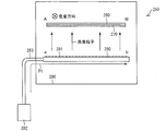
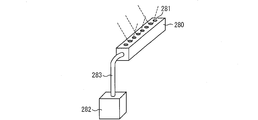
- FIG. 12 is a side view illustrating a schematic configuration of a conventional vapor deposition apparatus 250
- FIG. 13 is a perspective view illustrating a schematic configuration of a vapor deposition source 280, a vapor deposition source crucible 282, and a pipe 283 of the vapor deposition apparatus 250.
- the vapor deposition apparatus 250 is an apparatus for forming a film on the deposition target substrate 260, and includes a shadow mask 270, a vapor deposition source 280, a vapor deposition source crucible 282, and a pipe 283.
- the shadow mask 270 and the vapor deposition source 280 are disposed in the vacuum chamber 290, and the vapor deposition source crucible 282 is fixed to a support base (not shown).
- the vapor deposition source 280 has a plurality of injection ports (nozzles) 281 for injecting vapor deposition particles, and the injection ports 281 are arranged in one row as shown in FIG.
- the vapor deposition source crucible 282 stores a solid or liquid vapor deposition material.
- the vapor deposition material is heated inside the vapor deposition source crucible 282 to be gaseous vapor particles, and is supplied (introduced) to the vapor deposition source 280 through the pipe 283.
- the pipe 283 is connected to one end (supply side end) of the row of the injection ports 281 of the vapor deposition source 280, and the vapor deposition particles supplied to the vapor deposition source 280 are injected from the injection port 281. . Note that the pipe 283 is heated to a temperature at which vapor deposition particles do not adhere.
- the vapor deposition surface of the deposition target substrate 260 and the vapor deposition source 280 are arranged to face each other.
- a shadow mask 270 having an opening corresponding to the pattern of the vapor deposition region is closely fixed to the vapor deposition surface of the deposition target substrate 260 so that the vapor deposition particles do not adhere to a region other than the target vapor deposition region.
- the deposition target substrate 260 and the shadow mask 270 are relatively moved (scanned) with respect to the vapor deposition source 280 while vapor deposition particles are ejected from the ejection port 281. Thereby, a predetermined pattern is formed on the deposition target substrate 260.
- Japanese Patent Publication Japanese Patent Laid-Open No. 8-227276 (published on September 3, 1996)” Japanese Patent Publication “JP 2000-188179 A (published July 4, 2000)”
- the conventional technique as described above has a problem that the film thickness distribution of the deposited film becomes non-uniform.
- FIG. 14 is a graph showing the relationship between the position of the deposition target substrate 260 along the arrangement direction of the injection ports 281 and the distribution (thickness) of vapor deposition particles.
- a position facing the supply side end of the vapor deposition source 280 is A
- a position facing the end opposite to the supply side end of the vapor deposition source 280 is B.
- the inside of the vapor deposition source 280 is affected by the pressure difference in the supply path and the injection port, the internal shape, conductance, and the like, the amount of vapor deposition particles injected from each injection port 281 varies. Specifically, since the vapor deposition particles are sequentially injected from the injection port 281 near the supply side end portion, the density of the vapor deposition particles decreases as the distance from the supply side end portion increases, and a pressure difference is generated inside the vapor deposition source 280. Therefore, the larger the distance from the supply side end of the vapor deposition source 280, the smaller the injection amount of the vapor deposition particles from the injection port 281. Accordingly, as shown in FIG.
- the amount of vapor deposition particles varies depending on the position in the substrate surface for the vapor deposition film on the deposition target substrate 260 constituted by the synthesis of vapor deposition particles injected from various injection ports 281. Will be different. For this reason, nonuniformity of the film thickness distribution occurs in the substrate surface.
- the light emission characteristics of organic EL elements are extremely sensitive to the film thickness of the deposited organic film, and the difference in film thickness of the organic film within the screen of the organic EL display device results in uneven display and uneven life characteristics. Connect directly. Therefore, it is desirable to deposit the light emitting layer of the organic EL element as uniformly as possible.
- the present invention has been made in view of the above problems, and an object thereof is to provide a vapor deposition apparatus and a vapor deposition method capable of depositing vapor deposition particles with a uniform film thickness on a deposition target substrate.
- a vapor deposition apparatus is a vapor deposition apparatus that forms a film on a deposition target substrate, and has a plurality of injection ports that eject vapor deposition particles to the deposition target substrate.
- a vapor deposition source in which the injection ports are arranged in one or a plurality of rows, a plurality of pipes connected to the vapor deposition source, and a vapor deposition particle supply for supplying the vapor deposition particles to the vapor deposition source through the plurality of pipes And at least one of the plurality of pipes is connected to one end side of the row of the injection ports in the vapor deposition source, and at least one of the plurality of pipes is connected to the injection port of the vapor deposition source. It is characterized by being connected to the other end side of the row.
- a vapor deposition method is a vapor deposition method for forming a film on a deposition target substrate, which has a plurality of injection ports, and the injection ports are arranged in one or more rows.
- the vapor deposition source is supplied to the deposition target substrate from the injection port.
- the vapor deposition particles are connected to the vapor deposition source via a pipe connected to the other end side of the row of the injection ports in the vapor deposition source.
- the vapor deposition particles are supplied from the vapor deposition particle supply means to the vapor deposition source through a plurality of pipes, and are injected from the injection port onto the film formation substrate.
- first pipe a pipe connected to one end side of the row of injection ports in the vapor deposition source
- second pipe a pipe connected to the other end side of the row of injection ports in the vapor deposition source
- the injection amount of particles decreases monotonously.
- the film thickness distribution of the vapor deposition particles when the vapor deposition particles are supplied from the first pipe and the film thickness distribution of the vapor deposition particles when the vapor deposition particles are supplied from the second pipe are as follows. It becomes symmetric. Therefore, the film thickness distribution obtained by synthesizing these film thickness distributions is more uniform than the film thickness distribution when the vapor deposition is performed without rotating the vapor deposition source. Therefore, it is possible to provide a vapor deposition apparatus and a vapor deposition method capable of vapor deposition of vapor deposition particles with a uniform film thickness on a deposition target substrate.
- the organic electroluminescence display device manufacturing method of the present invention includes a TFT substrate / first electrode manufacturing step of forming a first electrode on a TFT substrate, and an organic layer on which an organic layer including at least a light emitting layer is deposited on the TFT substrate.
- An organic electroluminescence display device comprising: a vapor deposition step; a second electrode vapor deposition step of depositing a second electrode; and a sealing step of sealing an organic electroluminescence element including the organic layer and the second electrode with a sealing member.
- the organic layer or the like can be formed with a uniform film thickness by the vapor deposition method of the present invention, an organic electroluminescence display device with little display unevenness can be provided.
- the vapor deposition apparatus is a vapor deposition apparatus that forms a film on a film formation substrate, and has a plurality of injection holes for injecting vapor deposition particles onto the film formation substrate.
- Vapor deposition source arranged in one or more rows, a plurality of pipes connected to the vapor deposition source, vapor deposition particle supply means for supplying the vapor deposition particles to the vapor deposition source via the plurality of pipes, Moving means for moving the deposition target substrate relative to the deposition source, and at least one of the plurality of pipes is connected to one end side of the row of the injection ports in the deposition source, At least one of the pipes is configured to be connected to the other end side of the row of the injection ports in the vapor deposition source.
- the vapor deposition method according to the present invention is a vapor deposition method for forming a film on a deposition target substrate, wherein the vapor deposition source has a plurality of injection ports, and the injection ports are arranged in one or more rows.
- the injection port is configured to supply vapor deposition particles to the vapor deposition source through a pipe connected to one end side of the row of the injection ports in the source, and move the deposition target substrate relative to the vapor deposition source.
- the vapor deposition source was connected to the other end side of the row of the injection ports in the vapor deposition source Secondly, the vapor deposition particles are supplied to the vapor deposition source via a pipe, and the vapor deposition particles are ejected from the injection port to the film deposition substrate while moving the film deposition substrate relative to the vapor deposition source. Injection process. Therefore, there is an effect that it is possible to provide a vapor deposition apparatus and a vapor deposition method capable of depositing vapor deposition particles with a uniform film thickness on a deposition target substrate.
- FIG. 8 is a cross-sectional view taken along line AA of the TFT substrate in the organic EL display device shown in FIG.
- FIG. 1 It is a perspective view which shows schematic structure of the vapor deposition source unit of the vapor deposition apparatus shown in FIG. It is a graph which shows the relationship between the position in the film-forming substrate along the sequence direction of the injection port of a vapor deposition source, and distribution (thickness) of vapor deposition particles.
- a method for manufacturing a bottom emission type organic EL display device for RGB full color display in which light is extracted from the TFT substrate side is given as an example. explain.
- FIG. 6 is a sectional view showing a schematic configuration of an organic EL display device for RGB full-color display.
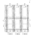
- 7 is a plan view showing a configuration of a pixel constituting the organic EL display device shown in FIG. 6, and
- FIG. 8 is a cross-sectional view taken along line AA of the TFT substrate in the organic EL display device shown in FIG. FIG.
- the organic EL display device 1 manufactured in the present embodiment includes an organic EL element 20 connected to the TFT 12 and an adhesive layer on the TFT substrate 10 on which the TFT 12 (see FIG. 8) is provided. 30 and the sealing substrate 40 have the structure provided in this order.
- the organic EL element 20 includes a pair of substrates (TFT substrates) by bonding the TFT substrate 10 on which the organic EL element 20 is laminated to a sealing substrate 40 using an adhesive layer 30. 10 and the sealing substrate 40).
- TFT substrates substrates
- the organic EL element 20 is sealed between the TFT substrate 10 and the sealing substrate 40 in this way, so that oxygen or moisture can enter the organic EL element 20 from the outside. It is prevented.
- the TFT substrate 10 includes a transparent insulating substrate 11 such as a glass substrate as a supporting substrate.
- a plurality of wirings 14 including a plurality of gate lines laid in the horizontal direction and a plurality of signal lines laid in the vertical direction and intersecting the gate lines are provided. It has been.
- a gate line driving circuit (not shown) for driving the gate line is connected to the gate line, and a signal line driving circuit (not shown) for driving the signal line is connected to the signal line.
- the organic EL display device 1 is a full-color active matrix organic EL display device, and red (R), green (G), and blue are respectively formed on the insulating substrate 11 in regions surrounded by the wirings 14.
- the sub-pixels 2R, 2G, and 2B of the respective colors including the organic EL elements 20 of the respective colors of (B) are arranged in a matrix.
- an area surrounded by these wirings 14 is one sub pixel (dot), and R, G, and B light emitting areas are defined for each sub pixel.
- the pixel 2 (that is, one pixel) has three sub-pixels: a red sub-pixel 2R that transmits red light, a green sub-pixel 2G that transmits green light, and a blue sub-pixel 2B that transmits blue light. It is composed of pixels 2R, 2G, and 2B.
- Each of the sub-pixels 2R, 2G, and 2B includes openings 15R and 15G that are covered by the light-emitting layers 23R, 23G, and 23B of the respective stripes as light-emitting regions of the respective colors that are responsible for light emission in the sub-pixels 2R, 2G, and 2B ⁇ 15B is provided.
- the light emitting layers 23R, 23G, and 23B are patterned by vapor deposition for each color.
- the openings 15R, 15G, and 15B will be described later.
- These sub-pixels 2R, 2G, and 2B are provided with TFTs 12 connected to the first electrode 21 in the organic EL element 20, respectively.
- the light emission intensity of each of the sub-pixels 2R, 2G, and 2B is determined by scanning and selection by the wiring 14 and the TFT 12.
- the organic EL display device 1 realizes image display by selectively causing the organic EL element 20 to emit light with desired luminance using the TFT 12.
- the TFT substrate 10 will be described.
- the TFT substrate 10 has a TFT 12 (switching element), an interlayer film 13 (interlayer insulating film, planarizing film), a wiring 14 and an edge cover 15 on a transparent insulating substrate 11 such as a glass substrate. It has the structure formed in this order.
- TFTs 12 are provided corresponding to the sub-pixels 2R, 2G, and 2B, respectively.
- the structure of the TFT is conventionally well known. Therefore, illustration and description of each layer in the TFT 12 are omitted.
- the interlayer film 13 is laminated on the insulating substrate 11 over the entire region of the insulating substrate 11 so as to cover the TFTs 12.
- the first electrode 21 in the organic EL element 20 is formed on the interlayer film 13.
- the interlayer film 13 is provided with a contact hole 13a for electrically connecting the first electrode 21 in the organic EL element 20 to the TFT 12.
- the TFT 12 is electrically connected to the organic EL element 20 through the contact hole 13a.
- the edge cover 15 prevents the first electrode 21 and the second electrode 26 in the organic EL element 20 from being short-circuited when the organic EL layer becomes thin or the electric field concentration occurs at the pattern end of the first electrode 21. It is an insulating layer for preventing.
- the edge cover 15 is formed on the interlayer film 13 so as to cover the pattern end of the first electrode 21.
- the edge cover 15 is provided with openings 15R, 15G, and 15B for each of the sub-pixels 2R, 2G, and 2B.
- the openings 15R, 15G, and 15B of the edge cover 15 are light emitting areas of the sub-pixels 2R, 2G, and 2B.
- the sub-pixels 2R, 2G, and 2B are partitioned by the edge cover 15 having an insulating property.
- the edge cover 15 also functions as an element isolation film.
- the organic EL element 20 is a light emitting element that can emit light with high luminance by low-voltage direct current drive, and a first electrode 21, an organic EL layer, and a second electrode 26 are laminated in this order.
- the first electrode 21 is a layer having a function of injecting (supplying) holes into the organic EL layer. As described above, the first electrode 21 is connected to the TFT 12 via the contact hole 13a.
- a hole injection layer / hole transport layer 22 As shown in FIG. 8, between the first electrode 21 and the second electrode 26, as an organic EL layer, from the first electrode 21 side, a hole injection layer / hole transport layer 22, and light emitting layers 23R, 23G, 23B, the electron carrying layer 24, and the electron injection layer 25 have the structure formed in this order.
- the stacking order is that in which the first electrode 21 is an anode and the second electrode 26 is a cathode, the first electrode 21 is a cathode, and the second electrode 26 is an anode.
- the order of stacking is reversed.
- the hole injection layer is a layer having a function of increasing the efficiency of hole injection into the light emitting layers 23R, 23G, and 23B.
- the hole transport layer is a layer having a function of improving the efficiency of transporting holes to the light emitting layers 23R, 23G, and 23B.
- the hole injection layer / hole transport layer 22 is uniformly formed on the entire display region of the TFT substrate 10 so as to cover the first electrode 21 and the edge cover 15.
- the hole injection layer / hole transport layer 22 in which the hole injection layer and the hole transport layer are integrated is provided as the hole injection layer and the hole transport layer.
- An example will be described.
- the present embodiment is not limited to this.
- the hole injection layer and the hole transport layer may be formed as independent layers.
- the light emitting layers 23R, 23G, and 23B correspond to the sub-pixels 2R, 2G, and 2B so as to cover the openings 15R, 15G, and 15B of the edge cover 15, respectively. Is formed.
- the light emitting layers 23R, 23G, and 23B are layers having a function of emitting light by recombining holes injected from the first electrode 21 side and electrons injected from the second electrode 26 side. .
- the light emitting layers 23R, 23G, and 23B are each formed of a material having high light emission efficiency, such as a low molecular fluorescent dye or a metal complex.
- the electron transport layer 24 is a layer having a function of increasing the electron transport efficiency from the second electrode 26 to the light emitting layers 23R, 23G, and 23B.
- the electron injection layer 25 is a layer having a function of increasing the electron injection efficiency from the second electrode 26 to the light emitting layers 23R, 23G, and 23B.
- the electron transport layer 24 is formed on the light emitting layer 23R / 23G / 23B and the hole injection layer / hole transport layer 22 so as to cover the light emitting layer 23R / 23G / 23B and the hole injection layer / hole transport layer 22.
- the TFT substrate 10 is formed uniformly over the entire display area. Further, the electron injection layer 25 is uniformly formed on the entire surface of the display region of the TFT substrate 10 on the electron transport layer 24 so as to cover the electron transport layer 24.
- the electron transport layer 24 and the electron injection layer 25 may be formed as independent layers as described above, or may be provided integrally with each other. That is, the organic EL display device 1 may include an electron transport layer / electron injection layer instead of the electron transport layer 24 and the electron injection layer 25.
- the second electrode 26 is a layer having a function of injecting electrons into the organic EL layer composed of the organic layers as described above.
- the second electrode 26 is uniformly formed on the entire surface of the display region of the TFT substrate 10 on the electron injection layer 25 so as to cover the electron injection layer 25.
- organic layers other than the light emitting layers 23R, 23G, and 23B are not essential layers as the organic EL layer, and may be appropriately formed according to the required characteristics of the organic EL element 20.
- a carrier blocking layer can also be added to the organic EL layer as necessary. For example, by adding a hole blocking layer as a carrier blocking layer between the light emitting layers 23R, 23G, and 23B and the electron transport layer 24, the holes are prevented from falling out to the electron transport layer 24, and the light emission efficiency is improved. can do.
- First electrode / light emitting layer / second electrode (2) First electrode / hole transport layer / light emitting layer / electron transport layer / second electrode (3) First electrode / hole transport layer / light emitting layer / Hole blocking layer (carrier blocking layer) / electron transport layer / second electrode (4) first electrode / hole transport layer / light emitting layer / hole blocking layer / electron transport layer / electron injection layer / second electrode (5 ) 1st electrode / hole injection layer / hole transport layer / light emitting layer / electron transport layer / electron injection layer / second electrode (6) 1st electrode / hole injection layer / hole transport layer / light emitting layer / positive Hole blocking layer / electron transport layer / second electrode (7) first electrode / hole injection layer / hole transport layer / light emitting layer / hole blocking layer / electron transport layer / electron injection layer / second electrode (8) 1st electrode
- the configuration of the organic EL element 20 is not limited to the above-described exemplary layer configuration, and a desired layer configuration can be adopted according to the required characteristics of the organic EL element 20 as described above.
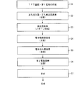
- FIG. 9 is a flowchart showing the manufacturing steps of the organic EL display device 1 in the order of steps.
- the manufacturing method of the organic EL display device 1 includes, for example, a TFT substrate / first electrode manufacturing step (S1), a hole injection layer / hole transport layer deposition configuration (S2). ), A light emitting layer vapor deposition step (S3), an electron transport layer vapor deposition step (S4), an electron injection layer vapor deposition step (S5), a second electrode vapor deposition step (S6), and a sealing step (S7).
- the stacking order described in the present embodiment uses the first electrode 21 as an anode and the second electrode 26 as a cathode, and conversely, uses the first electrode 21 as a cathode and the second electrode 26. Is used as the anode, the stacking order of the organic EL layers is reversed. Similarly, the materials constituting the first electrode 21 and the second electrode 26 are also reversed.
- a photosensitive resin is applied on an insulating substrate 11 such as glass on which TFTs 12 and wirings 14 are formed by a known technique, and patterning is performed by a photolithography technique, thereby insulating substrate 11.
- An interlayer film 13 is formed thereon.
- the insulating substrate 11 has a thickness of 0.7 to 1.1 mm, a length in the y-axis direction (vertical length) of 400 to 500 mm, and a length in the x-axis direction (horizontal length) of 300.
- a glass substrate or a plastic substrate of ⁇ 400 mm is used. In this embodiment, a glass substrate is used.
- an acrylic resin or a polyimide resin can be used as the interlayer film 13.
- the acrylic resin include Optomer series manufactured by JSR Corporation.
- a polyimide resin the photo nice series by Toray Industries, Inc. is mentioned, for example.
- the polyimide resin is generally not transparent but colored. Therefore, as shown in FIG. 8, when a bottom emission type organic EL display device is manufactured as the organic EL display device 1, a transparent resin such as an acrylic resin is more preferably used as the interlayer film 13. Used.
- the film thickness of the interlayer film 13 is not particularly limited as long as the step due to the TFT 12 can be compensated. In this embodiment, for example, the thickness is about 2 ⁇ m.
- a contact hole 13 a for electrically connecting the first electrode 21 to the TFT 12 is formed in the interlayer film 13.
- an ITO (Indium Tin Oxide: Indium Tin Oxide) film is formed with a thickness of 100 nm by a sputtering method or the like.
- the ITO film is etched using ferric chloride as an etchant. Thereafter, the photoresist is stripped using a resist stripping solution, and substrate cleaning is further performed. Thereby, the first electrode 21 is formed in a matrix on the interlayer film 13.
- Examples of the conductive film material used for the first electrode 21 include transparent conductive materials such as ITO, IZO (Indium (Zinc Oxide), gallium-doped zinc oxide (GZO), gold (Au), Metal materials such as nickel (Ni) and platinum (Pt) can be used.
- transparent conductive materials such as ITO, IZO (Indium (Zinc Oxide), gallium-doped zinc oxide (GZO), gold (Au), Metal materials such as nickel (Ni) and platinum (Pt) can be used.
- a method for laminating the conductive film in addition to the sputtering method, a vacuum deposition method, a CVD (chemical vapor deposition) method, a plasma CVD method, a printing method, or the like can be used.
- the thickness of the first electrode 21 is not particularly limited, but as described above, for example, the thickness can be set to 100 nm.
- the edge cover 15 is patterned and formed with a film thickness of, for example, about 1 ⁇ m.
- the same insulating material as that of the interlayer film 13 can be used.
- the TFT substrate 10 and the first electrode 21 are produced (S1).
- the TFT substrate 10 that has undergone the above-described steps is subjected to oxygen plasma treatment as a vacuum baking for dehydration and surface cleaning of the first electrode 21.
- a hole injection layer and a hole transport layer are displayed on the TFT substrate 10 on the TFT substrate 10 using a conventional vapor deposition apparatus. Vapor deposition is performed on the entire area (S2).
- an open mask having an entire display area opened is aligned and adhered to the TFT substrate 10 and then scattered from the deposition source while rotating the TFT substrate 10 and the open mask together. Vapor deposition particles are uniformly deposited on the entire display region through the opening of the open mask.
- vapor deposition on the entire surface of the display area means that vapor deposition is performed continuously between adjacent sub-pixels of different colors.
- Examples of the material for the hole injection layer and the hole transport layer include benzine, styrylamine, triphenylamine, porphyrin, triazole, imidazole, oxadiazole, polyarylalkane, phenylenediamine, arylamine, oxazole, anthracene, and fluorenone. , Hydrazone, stilbene, triphenylene, azatriphenylene, and derivatives thereof, polysilane compounds, vinylcarbazole compounds, thiophene compounds, aniline compounds, etc., heterocyclic or chain conjugated monomers, oligomers, or polymers Etc.
- the hole injection layer and the hole transport layer may be integrated as described above, or may be formed as independent layers.
- Each film thickness is, for example, 10 to 100 nm.
- the hole injection layer / hole transport layer 22 is provided as the hole injection layer and the hole transport layer, and the material of the hole injection layer / hole transport layer 22 is 4,4′-bis [ N- (1-naphthyl) -N-phenylamino] biphenyl ( ⁇ -NPD) was used.
- the film thickness of the hole injection layer / hole transport layer 22 was 30 nm.
- the light emitting layers 23R, 23G, and 23B corresponding to the sub-pixels 2R, 2G, and 2B so as to cover the openings 15R, 15G, and 15B of the edge cover 15. are separately formed (pattern formation) (S3).
- the light emitting layers 23R, 23G, and 23B are made of a material having high light emission efficiency such as a low molecular fluorescent dye or a metal complex.
- Examples of materials for the light emitting layers 23R, 23G, and 23B include anthracene, naphthalene, indene, phenanthrene, pyrene, naphthacene, triphenylene, anthracene, perylene, picene, fluoranthene, acephenanthrylene, pentaphen, pentacene, coronene, butadiene, and coumarin.
- the film thickness of the light emitting layers 23R, 23G, and 23B is, for example, 10 to 100 nm.
- the vapor deposition method and the vapor deposition apparatus according to the present embodiment can be particularly preferably used for such separate formation (pattern formation) of the light emitting layers 23R, 23G, and 23B.
- the electron transport layer 24, the hole injection layer / hole transport layer 22 and the light emitting layers 23R, 23G, and 23B are formed.
- the entire surface of the display area of the TFT substrate 10 is deposited so as to cover (S4).
- the electron injection layer 25 is formed on the entire surface of the display region of the TFT substrate 10 so as to cover the electron transport layer 24 by the same method as the hole injection layer / hole transport layer deposition step (S2). Evaporation is performed (S5).
- Examples of the material for the electron transport layer 24 and the electron injection layer 25 include tris (8-quinolinolato) aluminum complex, oxadiazole derivative, triazole derivative, phenylquinoxaline derivative, silole derivative and the like.
- Alq tris (8-hydroxyquinoline) aluminum
- anthracene naphthalene
- phenanthrene pyrene
- anthracene perylene
- butadiene coumarin
- acridine stilbene
- 1,10-phenanthroline and derivatives and metal complexes thereof
- the electron transport layer 24 and the electron injection layer 25 may be integrated or formed as independent layers.
- Each film thickness is, for example, 1 to 100 nm.
- the total film thickness of the electron transport layer 24 and the electron injection layer 25 is, for example, 20 to 200 nm.
- Alq is used as the material of the electron transport layer 24, and LiF is used as the material of the electron injection layer 25.
- the thickness of the electron transport layer 24 was 30 nm, and the thickness of the electron injection layer 25 was 1 nm.
- the second electrode 26 is applied to the entire display region of the TFT substrate 10 so as to cover the electron injection layer 25 by the same method as the hole injection layer / hole transport layer deposition step (S2). Evaporation is performed (S6).
- Electrode material of the second electrode 26 a metal having a small work function is preferably used.
- examples of such electrode materials include magnesium alloys (MgAg, etc.), aluminum alloys (AlLi, AlCa, AlMg, etc.), metallic calcium, and the like.
- the thickness of the second electrode 26 is, for example, 50 to 100 nm.
- the organic EL element 20 including the organic EL layer, the first electrode 21, and the second electrode 26 was formed on the TFT substrate 10.
- the TFT substrate 10 on which the organic EL element 20 was formed and the sealing substrate 40 were bonded together with an adhesive layer 30 to encapsulate the organic EL element 20.
- sealing substrate 40 for example, an insulating substrate such as a glass substrate or a plastic substrate having a thickness of 0.4 to 1.1 mm is used. In this embodiment, a glass substrate is used.
- the vertical length and the horizontal length of the sealing substrate 40 may be appropriately adjusted according to the size of the target organic EL display device 1, and an insulating substrate having substantially the same size as the insulating substrate 11 in the TFT substrate 10 is used. After sealing the organic EL element 20, the organic EL element 20 may be divided according to the size of the target organic EL display device 1.
- sealing method of the organic EL element 20 it is not limited to an above-described method.
- Other sealing methods include, for example, a method in which engraved glass is used as the sealing substrate 40 and sealing is performed in a frame shape with a sealing resin, frit glass, or the like, or between the TFT substrate 10 and the sealing substrate 40.
- a method of filling a resin in between The manufacturing method of the organic EL display device 1 does not depend on the sealing method, and any sealing method can be applied.
- a protective film (not shown) that prevents oxygen and moisture from entering the organic EL element 20 from the outside is provided on the second electrode 26 so as to cover the second electrode 26. Good.
- the protective film is made of an insulating or conductive material. Examples of such a material include silicon nitride and silicon oxide. Further, the thickness of the protective film is, for example, 100 to 1000 nm.
- the organic EL display device 1 is completed through the above steps.
- a predetermined image is displayed by controlling the light emission luminance of each of the sub-pixels 2R, 2G, and 2B.
- FIG. 1 is a side view showing a configuration of a vapor deposition apparatus 50 according to the present embodiment.
- the vapor deposition device 50 is a device that forms a film on the deposition target substrate 60, and includes a shadow mask 70, a vapor deposition source 80, a vapor deposition source crucible 82, and two pipes 83a and 83b.
- the shadow mask 70 and the vapor deposition source 80 are disposed in the vacuum chamber 90, and the vapor deposition source crucible 82 is fixed to a support base (not shown).
- the structures of the film formation substrate 60, the shadow mask 70, and the vapor deposition source crucible 82 are the same as those of the film formation substrate 260, the shadow mask 270, and the vapor deposition source crucible 282 shown in FIG.
- the vapor deposition source 80 has a plurality of ejection ports 81 through which vapor deposition particles are ejected, and the ejection ports 81 are arranged in a row as shown in FIG.
- the vapor deposition source crucible 82 stores a solid or liquid vapor deposition material. Further, the vapor deposition source crucible 82 is arranged outside the vacuum chamber 90. Thereby, it is not necessary to open the vacuum chamber 90 to the atmosphere each time the vapor deposition material is supplied to the vapor deposition source crucible 82, and the throughput can be improved. Further, a space can be provided in the vacuum chamber 90, and the design in the vacuum chamber 90 is facilitated.
- the vapor deposition material is heated inside the vapor deposition source crucible 82 to become gaseous vapor deposition particles, and is supplied (introduced) to the vapor deposition source 80 through the pipes 83a and 83b.
- One pipe 83 a is connected to one end face (referred to as “supply-side end face a”) of the row of the injection ports 81 of the vapor deposition source 80, and the other pipe 83 b is the injection port 81 of the vapor deposition source 80.
- supply-side end face b are connected to the other end surface (referred to as “supply-side end surface b”).
- the vapor deposition particles supplied to the vapor deposition source 80 are ejected from the ejection port 81.
- the vapor deposition surface of the deposition target substrate 60 and the vapor deposition source 80 are arranged to face each other.
- a shadow mask 70 having an opening corresponding to the pattern of the vapor deposition region is closely fixed to the vapor deposition surface of the deposition target substrate 60 so that the vapor deposition particles do not adhere to a region other than the target vapor deposition region. Then, the deposition target substrate 60 and the shadow mask 70 are moved relative to the deposition source 80 (scanned) by a moving unit (not shown) while ejecting the deposition particles from the injection port 81.
- the moving means moves the film formation substrate 60 and the shadow mask 70 in a direction perpendicular to the arrangement direction of the injection ports 81 ( It is reciprocated in the direction from the back side to the front side in the drawing and the opposite direction. As a result, a predetermined pattern is formed on the deposition target substrate 60.
- a pipe 283 for supplying vapor deposition particles is connected only to one end face of the row of the injection ports 281 of the vapor deposition source 280.
- the pipe 83a is connected to the end face on one end side of the row of the injection ports 81 of the vapor deposition source 80, and the other side of the row of the injection ports 81 of the vapor deposition source 80. It differs from the conventional vapor deposition apparatus 250 in that the pipe 83b is also connected to the end face on the end side.
- the pipes 83a and 83b are provided with valves 84a and 84b (supply control means), respectively.
- the valves 84a and 84b control the supply amount of the vapor deposition particles to the vapor deposition source 80 by opening and closing the internal paths of the pipes 83a and 83b, respectively.
- the valve 84a is open, the vapor deposition particles pass through the introduction path P1 indicated by the solid line arrow, and when the valve 84b is open, the vapor deposition particles pass through the introduction path P2 indicated by the broken line arrow.
- the introduction path is switched according to the scanning direction of the film formation substrate 60. Specifically, first, the valve 84a is opened, the vapor deposition particles are supplied to the vapor deposition source 80 through the pipe 83a, and the film formation substrate 60 is scanned in the back direction (the forward direction) in FIG. The vapor deposition particles are injected from 81 to the deposition target substrate 60 (first injection step). At this time, the valve 84b is closed.
- the valve 84a When scanning in the forward direction ends (that is, when the deposition target substrate 60 reaches a position not facing the vapor deposition source 80), the valve 84a is closed, and the supply of vapor deposition particles from the pipe 83a is terminated. Subsequently, the valve 84b is opened, the vapor deposition particles are supplied to the vapor deposition source 80 via the pipe 83b, and the film deposition substrate 60 is scanned from the injection port 81 while scanning in the forward direction (return direction) in FIG. The vapor deposition particles are injected onto the film formation substrate 60 (second injection step). When the scanning in the backward direction is finished, the ejection of the vapor deposition particles is finished.
- FIG. 3 is a graph showing the relationship between the position of the deposition target substrate 60 along the arrangement direction of the injection ports 81 and the distribution (thickness) of vapor deposition particles.
- the position facing the supply side end face a of the vapor deposition source 80 in the state of FIG. 1 is A
- the position facing the supply side end face b of the vapor deposition source 80 is B.
- the solid line indicates the distribution of vapor deposition particles when the film formation substrate 60 is scanned in the forward direction
- the broken line indicates the distribution of vapor deposition particles when the film formation substrate 60 is scanned in the double path direction.
- the alternate long and short dash line indicates the distribution of the vapor deposition particles when the reciprocating scanning is completed.
- the amount of vapor deposition particles emitted from the injection port 81 decreases as the distance from the supply side end surface of the vapor deposition source 80 increases. Therefore, the distribution of the vapor deposition particles when the deposition target substrate 60 is scanned in the forward direction (that is, when vapor deposition particles are supplied to the vapor deposition source 80 via the pipe 83a) is from the position A as indicated by the solid line. It gradually decreases toward B.
- the vapor deposition particles are supplied to the vapor deposition source 80 via the pipe 83b.
- the distribution of the injection amount of the vapor deposition particles injected onto the film formation substrate 60 is also reversed.
- the film thickness distribution when the deposition target substrate 60 scans in the backward direction is symmetric with respect to the film thickness distribution indicated by the solid line with respect to the intermediate position between the position A and the position B.
- the film thickness distribution at the time when the reciprocating scan of the deposition target substrate 60 is completed is the sum of the film thickness distribution indicated by the solid line and the film thickness distribution indicated by the broken line. Therefore, as shown by the alternate long and short dash line, the film thickness distribution is uniform when compared with the film thickness distribution when scanned in the forward direction and the film thickness distribution when scanned in the backward direction.
- the opening / closing switching of the valves 84a and 84b does not need to be performed every time the scanning direction of the deposition target substrate 60 is switched. For example, the film formation substrate 60 is reciprocated three times with the valve 84b closed and the valve 84a opened, and then the film formation substrate 60 is reciprocated three times with the valve 84a closed and the valve 84b opened. May be. Further, the switching of the valves 84 a and 84 b is performed when the deposition target substrate 60 passes over the deposition source 80 and is in a position where the deposition particles do not reach the deposition target substrate 60.
- valves 84a and 84b are opened, the amount of vapor deposition particles supplied from the respective pipes 83a and 83b to the vapor deposition source 80 changes due to a subtle difference in shape and conductance between the pipe 83a and the pipe 83b.
- the pressure distribution in the source 80 is also complicated, and it is difficult to make the film thickness distribution uniform. Therefore, it is preferable that the valves 84a and 84b are controlled so that both do not open simultaneously. However, if the influence of the pipes 83a and 83b is very small, both the valves 84a and 84b can be opened.
- the pipes 83a and 83b are connected to the end faces on the one end side and the other end side of the row of the injection ports 81 of the vapor deposition source 80.
- the positions where the pipes 83a and 83b are connected are not limited thereto. .
- pipes 83a and 83b may be connected to the vicinity of the end of the row of the injection ports 81 on the side surface in the longitudinal direction of the vapor deposition source 80A.
- FIG. 4B in the vapor deposition source 80A having a plurality of rows of injection ports 81, it is preferable to connect a plurality of pipes to each end face.
- two pipes 83a and 83c are connected to the end surface on one end side of the row of the injection ports 81 of the vapor deposition source 80A, and the end surface on the other end side of the row of the injection ports 81 of the vapor deposition source 80A.
- two pipes 83b and 83d are connected. Thereby, the nonuniformity of the injection quantity for every row
- the opening of the valves 84a and 84c of the pipes 83a and 83c and the opening of the valves 84b and 84d of the pipes 83b and 83d are alternately switched according to the switching in the scanning direction of the film formation substrate 60.
- the valves 83a and 84c of the pipes 83a and 83c are opened, and the valves 83b and 84d of the pipes 83b and 83d are closed, while the deposition target substrate 60 is scanned in the forward direction, the pipes 83a and 83c.
- the vapor deposition particles are supplied to the vapor deposition source 80, and the vapor deposition particles are ejected from the injection port 81 to the film formation substrate 60.
- valves 84 a and 84 c are closed, the valves 84 b and 84 d are opened, and the deposition particles are supplied to the deposition source 80 through the pipes 83 b and 83 d while scanning the deposition target substrate 60 in the backward direction.
- the vapor deposition particles are injected from 81 to the deposition target substrate 60.
- piping is connected to one end side and the other end side of the row of injection ports in the vapor deposition source, but the position where the piping is connected is not limited to this.
- the injection ports 81 are arranged in a matrix like the vapor deposition source 80B shown in FIG. 4C, pipes may be connected to the four sides of the vapor deposition source 80B.
- pipes 83a and 83b are respectively connected to one end side and the other end side of the row of the injection ports 81 in the vapor deposition source 80B.
- Pipes 83e and 83f are connected to one end side and the other end side of the row of injection ports 81 at 80B, respectively.
- valves 84a, 84b, 84e, and 84f of the pipes 83a, 83b, 83e, and 83f may be sequentially opened in accordance with switching in the scanning direction of the deposition target substrate 60, or all the valves 84a, 84b may be opened. -84e and 84f may be opened simultaneously.
- the deposition substrate and the shadow mask are in close contact with each other.
- vapor deposition may be performed by providing a gap between the deposition substrate and the shadow mask.
- a shadow mask that covers the entire surface of the deposition target substrate is used, but the present invention is not limited to this.
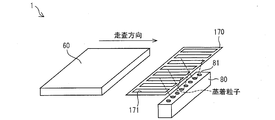
- a shadow mask 170 having a smaller area than the vapor deposition region of the deposition target substrate 60 may be used as the shadow mask.
- the relative position between the shadow mask 170 and the vapor deposition source 80 is fixed, and alignment is performed so that the shadow mask 170 faces the deposition target substrate with a certain gap. Then, the film formation substrate 60 is moved relative to the shadow mask 170 and the vapor deposition source 80, and vapor deposition particles are sequentially vapor deposited on the vapor deposition region of the film deposition substrate 60 through the opening 171 of the shadow mask 170.
- FIG. 10 is a side view showing the configuration of the vapor deposition apparatus 150 according to the present embodiment.
- the vapor deposition apparatus 150 is the structure further provided with the auxiliary piping 83g in the vapor deposition apparatus 50 shown in FIG.
- the auxiliary piping 83g is connected to an intermediate portion of the array of the injection ports 81 in the vapor deposition source 80.
- the vapor deposition source crucible 82 supplies vapor deposition particles to the vapor deposition source 80 via the pipes 83a and 83b and the auxiliary pipe 83g. That is, the vapor deposition particles are supplied to the vapor deposition source 80 from the introduction path P3 indicated by the one-dot chain line in addition to the introduction paths P1 and P2.
- auxiliary piping 83g is not provided with a valve. That is, vapor deposition particles are supplied to the vapor deposition source 80 from the auxiliary pipe 83g regardless of the scanning direction of the film formation substrate 60.
- the procedure of the vapor deposition process is the same as that in the first embodiment. Thereby, the vapor deposition apparatus 150 concerning this Embodiment can acquire the effect similar to the vapor deposition apparatus 50 concerning Embodiment 1.
- the auxiliary pipe 83g is provided, so that the film thickness distribution of the vapor deposition particles can be made more uniform. This will be described with reference to FIG.
- FIG. 11 is a graph showing the relationship between the position of the deposition target substrate 60 along the arrangement direction of the injection ports 81 and the distribution (thickness) of vapor deposition particles.
- the solid line indicates the distribution of vapor deposition particles when the film formation substrate 60 is scanned in the forward direction
- the broken line indicates the distribution of vapor deposition particles when the film formation substrate 60 is scanned in the double path direction.
- the alternate long and short dash line indicates the distribution of the vapor deposition particles when the reciprocating scanning is completed.
- the film thickness in the vicinity of the intermediate position is convex.
- the film thickness distribution of vapor deposition particle can be made more uniform compared with the film thickness distribution in the said Embodiment 1.
- auxiliary pipe is connected to a portion other than one end and the other end of the row of injection ports in the vapor deposition source.
- auxiliary pipe 83g may include a valve.
- a line type vapor deposition source in which injection ports are arranged in one row is used as the vapor deposition source.
- a surface type vapor deposition source in which a plurality of rows of injection ports are arranged may be used.
- pipes are respectively connected to one end surface and the other end surface of the row of injection ports in the vapor deposition source.
- deposition may be performed without moving the deposition target substrate relative to the deposition source.
- the arrangement direction of the injection ports is perpendicular to the scanning direction of the film formation substrate, but may be slightly deviated from the direction perpendicular to the scanning direction of the film formation substrate.
- the shape of the injection port is a point shape, but is not limited thereto, and may be, for example, a slit shape that is long in the arrangement direction of the injection ports.
- the present invention can also be applied to a contact-type scan vapor deposition method in which a film formation substrate is slid and vapor-deposited while the film formation substrate and a shadow mask are in close contact with each other. Further, the present invention can also be applied to the case where the deposition is performed on the entire surface of the deposition target substrate without using the shadow mask in which the opening pattern is formed for each sub-pixel as in S2 and S4 to S6 of FIG.
- the present invention can be applied not only to the deposition of an organic film but also to the deposition of a second electrode and the deposition of a sealing film.
- the variation in the thickness of the organic film greatly affects the characteristics of the organic EL display device, the application effect of the present invention is high.
- the film thickness variation of the second electrode affects the variation of electric resistance
- the variation of the sealing film affects the variation of moisture permeability and oxygen transmission rate. If the influence of these variations on the characteristics of the organic EL element is slight, the present invention may be applied only to the deposition of an organic film in view of the increase in equipment cost accompanying the complexity of the structure of the deposition apparatus. .
- a vapor deposition apparatus is a vapor deposition apparatus that forms a film on a deposition target substrate, and includes a plurality of injection ports that eject vapor deposition particles onto the deposition target substrate.
- a vapor deposition source in which the injection ports are arranged in one or a plurality of rows, a plurality of pipes connected to the vapor deposition source, and a vapor deposition particle supply for supplying the vapor deposition particles to the vapor deposition source via the plurality of pipes And at least one of the plurality of pipes is connected to one end side of the row of the injection ports in the vapor deposition source, and at least one of the plurality of pipes is connected to the injection port of the vapor deposition source Connected to the other end of the row.
- the vapor deposition method according to the embodiment of the present invention is a vapor deposition method for forming a film on a deposition target substrate, and has a plurality of injection ports, and the injection ports are arranged in one or a plurality of rows.
- the vapor deposition source is supplied to the deposition target substrate from the injection port.
- the vapor deposition particles are connected to the vapor deposition source via a pipe connected to the other end side of the row of the injection ports in the vapor deposition source.
- the vapor deposition particles are supplied from the vapor deposition particle supply means to the vapor deposition source through a plurality of pipes, and are injected from the injection port onto the film formation substrate.
- first pipe a pipe connected to one end side of the row of injection ports in the vapor deposition source
- second pipe a pipe connected to the other end side of the row of injection ports in the vapor deposition source
- the injection amount of particles decreases monotonously.
- the film thickness distribution of the vapor deposition particles when the vapor deposition particles are supplied from the first pipe and the film thickness distribution of the vapor deposition particles when the vapor deposition particles are supplied from the second pipe are as follows. It becomes symmetric. Therefore, the film thickness distribution obtained by synthesizing these film thickness distributions is more uniform than the film thickness distribution when the vapor deposition is performed without rotating the vapor deposition source. Therefore, it is possible to provide a vapor deposition apparatus and a vapor deposition method capable of vapor deposition of vapor deposition particles with a uniform film thickness on a deposition target substrate.
- each pipe preferably includes supply control means for controlling the supply amount of the vapor deposition particles to the vapor deposition source.
- the supply control means can switch ON / OFF the supply of vapor deposition particles from each pipe.
- vapor deposition particles can be vapor-deposited with a more uniform film thickness by switching the piping which supplies vapor deposition particles according to the switching of the relative movement direction of a film-forming substrate.
- the vapor deposition particles are supplied from any one of the plurality of pipes to the vapor deposition source when the vapor deposition particles are injected.
- a plurality of pipes are connected to the one end side and the other end side, respectively.
- the injection ports are arranged in a matrix, and at least one of the plurality of pipes is connected to one end side of the row of the injection ports in the vapor deposition source, It is preferable that at least one of the plurality of pipes is connected to the other end side of the row of the injection ports in the vapor deposition source.
- the film thickness distribution in the row direction of the injection port can be made uniform.
- the vapor deposition apparatus in addition to the plurality of pipes, the vapor deposition apparatus further includes an auxiliary pipe, and the vapor deposition particle supplying unit includes the vapor deposition particles via the plurality of pipes and the auxiliary pipe. Is preferably supplied to the vapor deposition source, and the auxiliary pipe is connected to a portion other than the one end and the other end of the vapor deposition source.
- the auxiliary pipe is connected to an intermediate portion of the array of the injection ports in the vapor deposition source.
- the vapor deposition apparatus preferably includes a moving means for moving the film formation substrate relative to the vapor deposition source.
- the arrangement direction of the plurality of injection ports is perpendicular to the direction in which the deposition target substrate is relatively moved.
- An organic electroluminescence display device manufacturing method includes a TFT substrate / first electrode manufacturing step of manufacturing a first electrode on a TFT substrate, and an organic layer including at least a light emitting layer on the TFT substrate.
- An organic layer deposition step for depositing the organic layer a second electrode deposition step for depositing the second electrode, and a sealing step for sealing the organic electroluminescence element including the organic layer and the second electrode with a sealing member.
- a second injection step is included.
- an organic layer or the like can be formed with a uniform film thickness by the vapor deposition method according to the embodiment of the present invention, so that an organic electroluminescence display device with little display unevenness can be provided. it can.
- the present invention can be applied not only to vapor deposition of vapor deposition particles in the manufacture of an organic EL display device but also to vapor deposition of vapor deposition particles to any film formation target.
- Organic EL display device (Organic electroluminescence display device) 2 pixel 2B sub pixel 2G sub pixel 2R sub pixel 10 TFT substrate 11 insulating substrate 12 TFT 13 Interlayer film 13a Contact hole 14 Wiring 15 Edge cover 15R Opening 15G Opening 15B Opening 20 Organic EL element 21 First electrode 22 Hole injection layer / hole transporting layer 23R Light emitting layer 23G Light emitting layer 23B Light emitting layer 24 Electron transport layer 25 Electron injection layer 26 Second electrode 30 Adhesive layer 40 Sealing substrate 50 Deposition device 60 Deposition substrate 70 Shadow mask 80 Deposition source 80A Deposition source 80B Deposition source 81 Injection port 82 Deposition source crucible (deposition particle supply means) 83a piping 83b piping 83c piping 83b piping 83d piping 83e piping 83f piping 83g auxiliary piping 84a valve (supply control means) 84b Valve (supply control means) 84c Valve (supply control means) 84d valve (suppl
Landscapes
- Chemical & Material Sciences (AREA)
- Engineering & Computer Science (AREA)
- Manufacturing & Machinery (AREA)
- Chemical Kinetics & Catalysis (AREA)
- Materials Engineering (AREA)
- Mechanical Engineering (AREA)
- Metallurgy (AREA)
- Organic Chemistry (AREA)
- Physics & Mathematics (AREA)
- Optics & Photonics (AREA)
- Electroluminescent Light Sources (AREA)
- Physical Vapour Deposition (AREA)
Abstract
Description
本発明の実施の一形態について図1~図9に基づいて説明すれば以下の通りである。
(1)第1電極/発光層/第2電極
(2)第1電極/正孔輸送層/発光層/電子輸送層/第2電極
(3)第1電極/正孔輸送層/発光層/正孔ブロッキング層(キャリアブロッキング層)/電子輸送層/第2電極
(4)第1電極/正孔輸送層/発光層/正孔ブロッキング層/電子輸送層/電子注入層/第2電極
(5)第1電極/正孔注入層/正孔輸送層/発光層/電子輸送層/電子注入層/第2電極
(6)第1電極/正孔注入層/正孔輸送層/発光層/正孔ブロッキング層/電子輸送層/第2電極
(7)第1電極/正孔注入層/正孔輸送層/発光層/正孔ブロッキング層/電子輸送層/電子注入層/第2電極
(8)第1電極/正孔注入層/正孔輸送層/電子ブロッキング層(キャリアブロッキング層)/発光層/正孔ブロッキング層/電子輸送層/電子注入層/第2電極
なお、上記したように、例えば正孔注入層と正孔輸送層とは、一体化されていてもよい。また、電子輸送層と電子注入層とは一体化されていてもよい。
本発明の実施の他の形態について、図10および図11に基づいて説明すれば以下の通りである。前記実施の形態1では、図3の一点鎖線で示される蒸着粒子の分布において、位置Aと位置Bとの中間位置の膜厚が、その他の位置の膜厚よりも小さくなっている。そこで、本実施形態では、補助用配管をさらに設けることにより、位置Aと位置Bとの中間位置付近の膜厚不足を解消する構成について説明する。なお、説明の便宜上、前記実施の形態1において説明した部材と同じ機能を有する部材については、同じ符号を付記し、その説明を省略する。
上記実施の形態では、蒸着源として、射出口が1列に配置されたライン型の蒸着源を用いていたが、射出口を複数列配置した面型の蒸着源を用いてもよい。この場合、蒸着源における射出口の列の一方端の面および他方端の面に、それぞれ配管が接続される。また、蒸着源の射出面が十分に大きく、被成膜基板が比較的小さい場合は、被成膜基板を蒸着源に対して相対移動させずに蒸着を行ってもよい。
以上のように、本発明の実施の形態に係る蒸着装置は、被成膜基板に成膜を行う蒸着装置であって、上記被成膜基板に蒸着粒子を射出する複数の射出口を有し、当該射出口が1列または複数列配置された蒸着源と、上記蒸着源に接続された複数の配管と、上記複数の配管を介して、上記蒸着粒子を上記蒸着源に供給する蒸着粒子供給手段とを備え、上記複数の配管の少なくとも1つは、上記蒸着源における上記射出口の列の一方端側に接続され、上記複数の配管の少なくとも1つは、上記蒸着源における上記射出口の列の他方端側に接続されている。
2 画素
2B サブ画素
2G サブ画素
2R サブ画素
10 TFT基板
11 絶縁基板
12 TFT
13 層間膜
13a コンタクトホール
14 配線
15 エッジカバー
15R 開口部
15G 開口部
15B 開口部
20 有機EL素子
21 第1電極
22 正孔注入層兼正孔輸送層
23R 発光層
23G 発光層
23B 発光層
24 電子輸送層
25 電子注入層
26 第2電極
30 接着層
40 封止基板
50 蒸着装置
60 被成膜基板
70 シャドウマスク
80 蒸着源
80A 蒸着源
80B 蒸着源
81 射出口
82 蒸着源坩堝(蒸着粒子供給手段)
83a 配管
83b 配管
83c 配管
83b 配管
83d 配管
83e 配管
83f 配管
83g 補助用配管
84a バルブ(供給制御手段)
84b バルブ(供給制御手段)
84c バルブ(供給制御手段)
84d バルブ(供給制御手段)
84e バルブ(供給制御手段)
84f バルブ(供給制御手段)
90 真空チャンバ
150 蒸着装置
170 シャドウマスク
171 開口部
250 蒸着装置
260 被成膜基板
270 シャドウマスク
280 蒸着源
281 射出口
282 蒸着源坩堝
283 配管
290 真空チャンバ
P1 導入経路
P2 導入経路
P3 導入経路
Claims (11)
- 被成膜基板に成膜を行う蒸着装置であって、
上記被成膜基板に蒸着粒子を射出する複数の射出口を有し、当該射出口が1列または複数列配置された蒸着源と、
上記蒸着源に接続された複数の配管と、
上記複数の配管を介して、上記蒸着粒子を上記蒸着源に供給する蒸着粒子供給手段と、
上記複数の配管の少なくとも1つは、上記蒸着源における上記射出口の列の一方端側に接続され、
上記複数の配管の少なくとも1つは、上記蒸着源における上記射出口の列の他方端側に接続されていることを特徴とする蒸着装置。 - 各配管は、上記蒸着粒子の上記蒸着源への供給量を制御する供給制御手段を備えていることを特徴とする請求項1に記載の蒸着装置。
- 上記蒸着粒子の射出時には、上記複数の配管のいずれか1つから上記蒸着粒子が上記蒸着源へ供給されることを特徴とする請求項2に記載の蒸着装置。
- 上記一方端側および上記他方端側には、それぞれ複数の配管が接続されることを特徴とする請求項1~3のいずれか1項に記載の蒸着装置。
- 上記射出口は、マトリクス状に配置され、
上記複数の配管の少なくとも1つは、上記蒸着源における上記射出口の行の一方端側に接続され、
上記複数の配管の少なくとも1つは、上記蒸着源における上記射出口の行の他方端側に接続されていることを特徴とする請求項1~4のいずれか1項に記載の蒸着装置。 - 上記複数の配管の他に、補助用配管をさらに備え、
上記蒸着粒子供給手段は、上記複数の配管および上記補助用配管を介して、上記蒸着粒子を上記蒸着源に供給し、
上記補助用配管は、上記蒸着源における上記一方端および他方端以外の部分に接続されることを特徴とする請求項1~5のいずれか1項に記載の蒸着装置。 - 上記補助用配管は、上記蒸着源における上記射出口の配列の中間部分に接続されることを特徴とする請求項6に記載の蒸着装置。
- 上記被成膜基板を上記蒸着源に対して相対移動させる移動手段を備えることを特徴とする請求項1~7のいずれか1項に記載の蒸着装置。
- 上記複数の射出口の配列方向は、上記被成膜基板が相対移動する方向に垂直であることを特徴とする請求項1~8のいずれか1項に記載の蒸着装置。
- 被成膜基板に成膜を行う蒸着方法であって、
複数の射出口を有し、当該射出口が1列または複数列配置された蒸着源に、上記蒸着源における上記射出口の列の一方端側に接続された配管を介して、蒸着粒子を上記蒸着源に供給しながら、上記射出口から上記被成膜基板に上記蒸着粒子を射出する第1の射出工程と、
第1の射出工程の後に、上記蒸着源に、上記蒸着源における上記射出口の列の他方端側に接続された配管を介して、蒸着粒子を上記蒸着源に供給しながら、上記射出口から上記被成膜基板に上記蒸着粒子を射出する第2の射出工程とを有していることを特徴とする蒸着方法。 - TFT基板上に第1電極を作製するTFT基板・第1電極作製工程と、
上記TFT基板上に少なくとも発光層を含む有機層を蒸着する有機層蒸着工程と、
第2電極を蒸着する第2電極蒸着工程と、
上記有機層および第2電極を含む有機エレクトロルミネッセンス素子を封止部材で封止する封止工程とを有する有機エレクトロルミネッセンス表示装置の製造方法であって、
上記有機層蒸着工程、上記第2電極蒸着工程、および上記封止工程の少なくともいずれかの工程は、請求項10に記載の蒸着方法の上記第1の射出工程および上記第2の射出工程を有することを特徴とする有機エレクトロルミネッセンス表示装置の製造方法。
Priority Applications (3)
| Application Number | Priority Date | Filing Date | Title |
|---|---|---|---|
| US13/993,677 US20130260501A1 (en) | 2010-12-21 | 2011-12-14 | Vapor deposition device, vapor deposition method, and method of manufacturing organic electroluminescent display device |
| JP2012549744A JP5410618B2 (ja) | 2010-12-21 | 2011-12-14 | 蒸着装置、蒸着方法、並びに、有機エレクトロルミネッセンス表示装置の製造方法 |
| US14/879,090 US20160036008A1 (en) | 2010-12-21 | 2015-10-08 | Method of manufacturing film formation substrate, and method of manufacturing organic electroluminescent display device |
Applications Claiming Priority (2)
| Application Number | Priority Date | Filing Date | Title |
|---|---|---|---|
| JP2010-284504 | 2010-12-21 | ||
| JP2010284504 | 2010-12-21 |
Related Child Applications (2)
| Application Number | Title | Priority Date | Filing Date |
|---|---|---|---|
| US13/993,677 A-371-Of-International US20130260501A1 (en) | 2010-12-21 | 2011-12-14 | Vapor deposition device, vapor deposition method, and method of manufacturing organic electroluminescent display device |
| US14/879,090 Continuation US20160036008A1 (en) | 2010-12-21 | 2015-10-08 | Method of manufacturing film formation substrate, and method of manufacturing organic electroluminescent display device |
Publications (1)
| Publication Number | Publication Date |
|---|---|
| WO2012086480A1 true WO2012086480A1 (ja) | 2012-06-28 |
Family
ID=46313756
Family Applications (1)
| Application Number | Title | Priority Date | Filing Date |
|---|---|---|---|
| PCT/JP2011/078861 Ceased WO2012086480A1 (ja) | 2010-12-21 | 2011-12-14 | 蒸着装置、蒸着方法、並びに、有機エレクトロルミネッセンス表示装置の製造方法 |
Country Status (3)
| Country | Link |
|---|---|
| US (2) | US20130260501A1 (ja) |
| JP (1) | JP5410618B2 (ja) |
| WO (1) | WO2012086480A1 (ja) |
Cited By (2)
| Publication number | Priority date | Publication date | Assignee | Title |
|---|---|---|---|---|
| JP2014123505A (ja) * | 2012-12-21 | 2014-07-03 | Konica Minolta Inc | 蒸着装置及び蒸着方法 |
| WO2015159428A1 (ja) * | 2014-04-18 | 2015-10-22 | 長州産業株式会社 | ラインソース |
Families Citing this family (5)
| Publication number | Priority date | Publication date | Assignee | Title |
|---|---|---|---|---|
| JP5512881B2 (ja) * | 2011-03-30 | 2014-06-04 | シャープ株式会社 | 蒸着処理システム及び蒸着処理方法 |
| KR20180015250A (ko) * | 2015-07-28 | 2018-02-12 | 샤프 가부시키가이샤 | 증착원, 증착 장치 및 증착막 제조 방법 |
| KR20220090667A (ko) * | 2020-12-22 | 2022-06-30 | 삼성디스플레이 주식회사 | 발광 소자 및 이를 포함한 전자 장치 |
| CN113054124A (zh) * | 2021-02-20 | 2021-06-29 | 京东方科技集团股份有限公司 | 一种有机发光器件、显示装置、制作方法以及存储介质 |
| US20230208091A1 (en) * | 2021-12-29 | 2023-06-29 | River Electro-Optics, LLC | Distributed gain polygon ring laser amplification |
Citations (5)
| Publication number | Priority date | Publication date | Assignee | Title |
|---|---|---|---|---|
| JP2002184571A (ja) * | 2000-12-15 | 2002-06-28 | Denso Corp | 有機el素子の製造方法 |
| JP2007332458A (ja) * | 2006-05-18 | 2007-12-27 | Sony Corp | 蒸着装置および蒸着源ならびに表示装置の製造方法 |
| JP2008019477A (ja) * | 2006-07-13 | 2008-01-31 | Canon Inc | 真空蒸着装置 |
| JP2011068916A (ja) * | 2009-09-22 | 2011-04-07 | Toshiba Corp | 成膜方法および成膜装置 |
| JP2011122187A (ja) * | 2009-12-08 | 2011-06-23 | Ulvac Japan Ltd | 材料蒸発システム及びその成膜装置 |
Family Cites Families (9)
| Publication number | Priority date | Publication date | Assignee | Title |
|---|---|---|---|---|
| US3850679A (en) * | 1972-12-15 | 1974-11-26 | Ppg Industries Inc | Chemical vapor deposition of coatings |
| KR100201386B1 (ko) * | 1995-10-28 | 1999-06-15 | 구본준 | 화학기상증착장비의 반응가스 분사장치 |
| JP3019095B1 (ja) * | 1998-12-22 | 2000-03-13 | 日本電気株式会社 | 有機薄膜elデバイスの製造方法 |
| ATE374263T1 (de) * | 1999-03-29 | 2007-10-15 | Antec Solar Energy Ag | Vorrichtung und verfahren zur beschichtung von substraten durch aufdampfen mittels eines pvd- verfahrens |
| JP4704605B2 (ja) * | 2001-05-23 | 2011-06-15 | 淳二 城戸 | 連続蒸着装置、蒸着装置及び蒸着方法 |
| TWI252706B (en) * | 2002-09-05 | 2006-04-01 | Sanyo Electric Co | Manufacturing method of organic electroluminescent display device |
| EP1862788A1 (en) * | 2006-06-03 | 2007-12-05 | Applied Materials GmbH & Co. KG | Evaporator for organic material, coating installation, and method for use thereof |
| EP2168643A1 (en) * | 2008-09-29 | 2010-03-31 | Applied Materials, Inc. | Evaporator for organic materials |
| KR100977374B1 (ko) * | 2009-08-03 | 2010-08-20 | 텔리오솔라 테크놀로지스 인크 | 대면적 박막형 cigs 태양전지 고속증착 및 양산장비, 그 공정방법 |
-
2011
- 2011-12-14 JP JP2012549744A patent/JP5410618B2/ja not_active Expired - Fee Related
- 2011-12-14 WO PCT/JP2011/078861 patent/WO2012086480A1/ja not_active Ceased
- 2011-12-14 US US13/993,677 patent/US20130260501A1/en not_active Abandoned
-
2015
- 2015-10-08 US US14/879,090 patent/US20160036008A1/en not_active Abandoned
Patent Citations (5)
| Publication number | Priority date | Publication date | Assignee | Title |
|---|---|---|---|---|
| JP2002184571A (ja) * | 2000-12-15 | 2002-06-28 | Denso Corp | 有機el素子の製造方法 |
| JP2007332458A (ja) * | 2006-05-18 | 2007-12-27 | Sony Corp | 蒸着装置および蒸着源ならびに表示装置の製造方法 |
| JP2008019477A (ja) * | 2006-07-13 | 2008-01-31 | Canon Inc | 真空蒸着装置 |
| JP2011068916A (ja) * | 2009-09-22 | 2011-04-07 | Toshiba Corp | 成膜方法および成膜装置 |
| JP2011122187A (ja) * | 2009-12-08 | 2011-06-23 | Ulvac Japan Ltd | 材料蒸発システム及びその成膜装置 |
Cited By (2)
| Publication number | Priority date | Publication date | Assignee | Title |
|---|---|---|---|---|
| JP2014123505A (ja) * | 2012-12-21 | 2014-07-03 | Konica Minolta Inc | 蒸着装置及び蒸着方法 |
| WO2015159428A1 (ja) * | 2014-04-18 | 2015-10-22 | 長州産業株式会社 | ラインソース |
Also Published As
| Publication number | Publication date |
|---|---|
| JP5410618B2 (ja) | 2014-02-05 |
| US20130260501A1 (en) | 2013-10-03 |
| JPWO2012086480A1 (ja) | 2014-05-22 |
| US20160036008A1 (en) | 2016-02-04 |
Similar Documents
| Publication | Publication Date | Title |
|---|---|---|
| JP5330608B2 (ja) | 蒸着装置、蒸着方法、並びに、有機エレクトロルミネッセンス表示装置の製造方法 | |
| CN103430625B (zh) | 蒸镀装置、蒸镀方法和有机el显示装置的制造方法 | |
| JP6567349B2 (ja) | 蒸着方法及び蒸着装置 | |
| JP5826828B2 (ja) | 表示用基板、有機エレクトロルミネッセンス表示装置、およびそれらの製造方法 | |
| JP5410618B2 (ja) | 蒸着装置、蒸着方法、並びに、有機エレクトロルミネッセンス表示装置の製造方法 | |
| JP6199967B2 (ja) | 有機エレクトロルミネッセンス素子の製造方法 | |
| WO2012124512A1 (ja) | 蒸着装置、蒸着方法、及び有機el表示装置 | |
| WO2012099011A1 (ja) | 被成膜基板、製造方法、および有機el表示装置 | |
| WO2012099019A1 (ja) | 被成膜基板、有機el表示装置および蒸着方法 | |
| WO2012098994A1 (ja) | 被成膜基板、有機el表示装置 | |
| JP5718362B2 (ja) | 蒸着装置、蒸着方法、並びに、有機エレクトロルミネッセンス表示装置の製造方法 | |
| TWI506152B (zh) | 被成膜基板、有機el顯示裝置 | |
| US9614155B2 (en) | Vapor deposition apparatus, vapor deposition method, and method for producing organic electroluminescent element |
Legal Events
| Date | Code | Title | Description |
|---|---|---|---|
| 121 | Ep: the epo has been informed by wipo that ep was designated in this application |
Ref document number: 11850249 Country of ref document: EP Kind code of ref document: A1 |
|
| ENP | Entry into the national phase |
Ref document number: 2012549744 Country of ref document: JP Kind code of ref document: A |
|
| WWE | Wipo information: entry into national phase |
Ref document number: 13993677 Country of ref document: US |
|
| NENP | Non-entry into the national phase |
Ref country code: DE |
|
| 122 | Ep: pct application non-entry in european phase |
Ref document number: 11850249 Country of ref document: EP Kind code of ref document: A1 |