WO2012086396A1 - 有機el素子および透光性基板 - Google Patents
有機el素子および透光性基板 Download PDFInfo
- Publication number
- WO2012086396A1 WO2012086396A1 PCT/JP2011/078106 JP2011078106W WO2012086396A1 WO 2012086396 A1 WO2012086396 A1 WO 2012086396A1 JP 2011078106 W JP2011078106 W JP 2011078106W WO 2012086396 A1 WO2012086396 A1 WO 2012086396A1
- Authority
- WO
- WIPO (PCT)
- Prior art keywords
- light extraction
- layer
- protrusion
- refractive index
- extraction layer
- Prior art date
- Legal status (The legal status is an assumption and is not a legal conclusion. Google has not performed a legal analysis and makes no representation as to the accuracy of the status listed.)
- Ceased
Links
Images






Classifications
-
- G—PHYSICS
- G02—OPTICS
- G02B—OPTICAL ELEMENTS, SYSTEMS OR APPARATUS
- G02B5/00—Optical elements other than lenses
- G02B5/02—Diffusing elements; Afocal elements
- G02B5/0205—Diffusing elements; Afocal elements characterised by the diffusing properties
- G02B5/0236—Diffusing elements; Afocal elements characterised by the diffusing properties the diffusion taking place within the volume of the element
-
- G—PHYSICS
- G02—OPTICS
- G02B—OPTICAL ELEMENTS, SYSTEMS OR APPARATUS
- G02B5/00—Optical elements other than lenses
- G02B5/02—Diffusing elements; Afocal elements
- G02B5/0205—Diffusing elements; Afocal elements characterised by the diffusing properties
- G02B5/021—Diffusing elements; Afocal elements characterised by the diffusing properties the diffusion taking place at the element's surface, e.g. by means of surface roughening or microprismatic structures
- G02B5/0231—Diffusing elements; Afocal elements characterised by the diffusing properties the diffusion taking place at the element's surface, e.g. by means of surface roughening or microprismatic structures the surface having microprismatic or micropyramidal shape
-
- H—ELECTRICITY
- H10—SEMICONDUCTOR DEVICES; ELECTRIC SOLID-STATE DEVICES NOT OTHERWISE PROVIDED FOR
- H10K—ORGANIC ELECTRIC SOLID-STATE DEVICES
- H10K50/00—Organic light-emitting devices
- H10K50/80—Constructional details
- H10K50/85—Arrangements for extracting light from the devices
- H10K50/854—Arrangements for extracting light from the devices comprising scattering means
-
- H—ELECTRICITY
- H10—SEMICONDUCTOR DEVICES; ELECTRIC SOLID-STATE DEVICES NOT OTHERWISE PROVIDED FOR
- H10K—ORGANIC ELECTRIC SOLID-STATE DEVICES
- H10K50/00—Organic light-emitting devices
- H10K50/80—Constructional details
- H10K50/85—Arrangements for extracting light from the devices
- H10K50/858—Arrangements for extracting light from the devices comprising refractive means, e.g. lenses
-
- H—ELECTRICITY
- H10—SEMICONDUCTOR DEVICES; ELECTRIC SOLID-STATE DEVICES NOT OTHERWISE PROVIDED FOR
- H10K—ORGANIC ELECTRIC SOLID-STATE DEVICES
- H10K77/00—Constructional details of devices covered by this subclass and not covered by groups H10K10/80, H10K30/80, H10K50/80 or H10K59/80
- H10K77/10—Substrates, e.g. flexible substrates
-
- Y—GENERAL TAGGING OF NEW TECHNOLOGICAL DEVELOPMENTS; GENERAL TAGGING OF CROSS-SECTIONAL TECHNOLOGIES SPANNING OVER SEVERAL SECTIONS OF THE IPC; TECHNICAL SUBJECTS COVERED BY FORMER USPC CROSS-REFERENCE ART COLLECTIONS [XRACs] AND DIGESTS
- Y10—TECHNICAL SUBJECTS COVERED BY FORMER USPC
- Y10T—TECHNICAL SUBJECTS COVERED BY FORMER US CLASSIFICATION
- Y10T428/00—Stock material or miscellaneous articles
- Y10T428/24—Structurally defined web or sheet [e.g., overall dimension, etc.]
- Y10T428/24479—Structurally defined web or sheet [e.g., overall dimension, etc.] including variation in thickness
- Y10T428/24612—Composite web or sheet
Definitions
- the present invention relates to an organic EL element.
- Organic electroluminescence (organic EL) elements are widely used for displays, backlights, lighting applications, and the like.
- a general organic EL element has a first electrode (anode) placed on a support substrate, a second electrode (cathode), and an organic light emitting layer placed between these electrodes.
- a voltage is applied between the electrodes, holes and electrons are injected from each electrode into the organic light emitting layer.
- binding energy is generated, and the light emitting material in the organic light emitting layer is excited by this binding energy. Since light emission occurs when the excited light emitting material returns to the ground state, a light emitting (EL) element can be obtained by utilizing this.
- a transparent thin film such as ITO (Indium Tin Oxide) is used for the first electrode, that is, the anode, and a metal thin film such as aluminum and silver is used for the second electrode, that is, the cathode.
- ITO Indium Tin Oxide
- Patent Document 1 proposes a resin light extraction layer between the first electrode and the support substrate. For example, it is disclosed that the external extraction efficiency of light generated in the organic layer can be increased by installing a resin light extraction layer having periodic unevenness between the first electrode and the support substrate.
- Patent Document 2 a method for improving the light extraction efficiency by providing a scattering material in the light extraction layer is disclosed.
- the light extraction layer is made of resin, the following problems may occur.
- the resin used for the light extraction layer is usually hygroscopic. For this reason, when the resin light extraction layer is used for a long time, the light extraction layer may be deteriorated or colored. When such deterioration or coloring occurs in the light extraction layer, the light emission efficiency of the organic EL element decreases.
- the light extraction layer usually needs to have a high refractive index. This is because the refractive index of the anode (ITO (Indium Tin Oxide) electrode) is relatively high, and when a light extraction layer with a low refractive index is used, there is a high possibility that total reflection will occur at the interface between the two. Because. However, it is difficult to form such a high refractive index light extraction layer with a resin.
- ITO Indium Tin Oxide
- the conventional resin light extraction layer has problems in terms of environmental resistance and refractive index.
- the present invention has been made in view of such problems, and the present invention provides an organic EL device having a light extraction layer having good environmental resistance and a high refractive index, and having good light extraction efficiency. For the purpose. Moreover, it aims at providing the translucent board
- the translucent substrate according to the first aspect of the present invention includes a transparent support substrate and glass having a first refractive index which is formed on the transparent support substrate and is in the range of 1.6 to 2.2 at the D line.
- a light extraction layer having a material and a scattering material having a second refractive index different from the first refractive index in the D line, and the surface of the light extraction layer has a substantially pyramid having one vertex.
- a substantially triangular prism-shaped projection having one top side, and is obtained in a vertical cross section passing through the top point of the projection or a cross section perpendicular to the top side of the projection.
- at least one of the angles formed between the base of the substantially triangular shape and the other sides is in the range of 10 ° to 60 °.
- the translucent substrate according to the second aspect of the present invention is a transparent support substrate and glass having a first refractive index formed on the transparent support substrate and in the range of 1.6 to 2.2 at the D line. And a light extraction layer substantially free of a scattering material having a second refractive index different from the first refractive index, the surface of the light extraction layer having one top
- a substantially pyramid-shaped protrusion having a point or a substantially triangular prism-shaped protrusion having one top side is formed, and a vertical cross section passing through the top point of the protrusion or a cross section perpendicular to the top side of the protrusion
- At least one angle ⁇ among the angles formed by the base of the substantially triangular shape and the other sides obtained in is in the range of 5 ° to 70 °.
- the scattering material may be a precipitated crystal of glass constituting at least one of bubbles and the glass material.
- the angle ⁇ may be in the range of 15 ° to 40 °.
- the protrusions may not be arranged periodically.
- the protrusions may be periodically arranged when the bottom dimension is outside the range of 0.1 ⁇ m to 100 ⁇ m.
- the organic EL device of the present invention includes the above-described translucent substrate, a first electrode formed on the light extraction layer, an organic light emitting layer formed on the first electrode, and the organic A second electrode formed on the light emitting layer.
- an organic EL element having a light extraction layer having good environmental resistance and a high refractive index and having good light extraction efficiency.
- substrate which can be used for such an organic EL element can be provided.
- FIG. 1 shows a simplified cross-sectional view of a conventional organic EL element.
- the conventional organic EL element 1 includes a translucent substrate 5, a first electrode (anode) 70, an organic light emitting layer 80, and a second electrode (cathode) 90 in this order. It is configured by stacking.
- the translucent substrate 5 is configured by laminating a light extraction layer 20 on a support substrate 10.
- the lower surface of the organic EL element 1 (that is, the exposed surface of the support substrate 10) is the light extraction surface 60.
- the light extraction layer 20 has a role of scattering incident light in a plurality of directions. Therefore, in the organic EL element 1 having the light extraction layer 20, attenuation of light emitted from the light extraction layer 80 can be suppressed, and compared with a configuration without the light extraction layer 20, the light extraction surface 60 can be used. The amount of emitted light can be improved.
- the light extraction layer 20 is made of resin.
- the resin used for the light extraction layer 20 usually has hygroscopicity. For this reason, when the light extraction layer 20 is used for a long time, the light extraction layer 20 may be deteriorated or colored. When such deterioration or coloring occurs in the light extraction layer 20, the light emission efficiency of the organic EL element 1 is lowered.
- the light extraction layer 20 is usually desired to have a high refractive index.
- the first electrode usually an ITO (indium tin oxide) electrode
- ITO indium tin oxide
- the resin it is difficult to form a light extraction layer of such a high refractive index (usually, the refractive index n d of the resin is about 1.4-1.6).
- the conventional resin light extraction layer 20 has problems in terms of environmental resistance and refractive index.
- the present invention has a feature that the light extraction layer is made of glass having a relatively high refractive index.
- the refractive index n d is in the range 1.6 to 2.2.
- the present invention has another feature that a periodic pattern is formed on the surface of the light extraction layer by a substantially pyramidal projection or a substantially triangular prismatic projection.
- Patent Document 1 discloses forming a concavo-convex structure in a resin light extraction layer.
- the optimum pattern of the concavo-convex shape is sufficiently disclosed, and the light extraction layer having any concavo-convex shape pattern can provide sufficient light extraction efficiency. It is unknown.
- the surface of the light extraction layer has a periodic pattern of substantially pyramidal projections having one “top point” and the “tilt angle” is in the range of 5 ° to 70 °.
- top point means a vertex that is farthest from the interface between the light extraction layer and the support substrate (hereinafter simply referred to as “interface”) among the vertexes included in the pyramid. To do. For example, in the case of a pyramid other than a triangular pyramid, the most side extends from the “top point” (however, in the case of a triangular pyramid, the number of sides extending from each vertex is 3).
- inclination angle means the angle (there are two) between the side passing through the “top point” of the approximate triangle obtained in the vertical cross section passing through the “top point” of the protrusion and the bottom side.
- substantially triangular does not intend to include only those whose apex angles are acute angles, but rather include those whose apexes are rounded in the manufacturing process.
- the surface of the light extraction layer has a periodic pattern of substantially triangular prism-shaped protrusions having one “top side” and the “inclination angle” is in the range of 5 ° to 70 °.
- top side means a side farthest from the “interface” among the sides extending in the axial direction included in the substantially triangular prism.
- the “inclination angle” is the larger of the angle (two exist) between the side passing through the apex of the substantially triangular shape and the base obtained in the vertical cross section passing through the “top side” of the protrusion. Means.
- the surface of the light extraction layer has a periodic or non-periodic pattern due to a substantially pyramidal protrusion having one apex point, or a periodic or aperiodic pattern due to a substantially triangular prism-shaped protrusion having one apex side. At least one of an angle formed between a base of the substantially triangular shape and other sides obtained in a vertical cross section passing through the top point of the protrusion or a cross section perpendicular to the top side of the protrusion. One angle is in the range of 5 ° to 70 °.
- the organic EL device according to the present invention can obtain good environmental resistance and can obtain significant light extraction efficiency as compared with the conventional case.
- the “inclination angle” is defined by taking as an example a case where the top point or the top side is clearly recognized.
- the “tilt angle” is as follows. Can be requested. That is, in the case of (i), the “top point” of the protrusion can be determined by extrapolating a plurality of ridge lines of the protrusion in a straight line and obtaining the intersection. In addition, the inclination angle is based on the approximate triangle obtained in the vertical section passing through the “top point” thus determined (if necessary, the side passing through the “top point” of the obtained approximate triangle. Can be determined by linear extrapolation).
- the “top side” of the protrusion can be determined by extrapolating the inclined surface of the protrusion in a straight line and obtaining the intersection.
- the inclination angle is based on the approximate triangle obtained in the vertical cross section passing through the “top side” determined in this way (if necessary, the inclination plane passing through the apex of the obtained approximate triangle is a straight line. Can be determined by extrapolation).
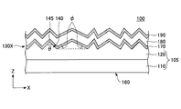
- FIG. 2 shows an example of a schematic partial cross-sectional view of an organic EL element according to the present invention.
- FIG. 2A is a partial cross-sectional view showing a case where the protrusion of the light extraction layer has periodicity
- FIG. 2B shows a case where the protrusion of the light extraction layer has no periodicity (random).
- FIG. 2A when the bottom dimension constituting the protrusion is within the range of 0.1 ⁇ m to 100 ⁇ m, the structure of FIG. 2B is preferable, and the bottom dimension constituting the protrusion is 0.1 ⁇ m to 100 ⁇ m. If it is out of the range, the configuration shown in FIG.
- the base dimension is in the range of 0.1 ⁇ m to 100 ⁇ m
- the arrangement of the protrusions is periodic, light may be diffracted and interfered. There may be a problem that the light appears to be iridescent. Therefore, when the bottom dimension is in the range of 0.1 ⁇ m to 100 ⁇ m, it is preferable that the arrangement of the protrusions has no periodicity.
- the protrusions may be periodically arranged.
- the base dimension is out of the range of 0.1 ⁇ m to 100 ⁇ m, light interference does not occur even if the protrusions are arranged periodically, so that the protrusions may be arranged randomly or periodically.
- the organic EL device 100 includes a translucent substrate 105, a first electrode (anode) 170, an organic light emitting layer 180, and a second electrode (cathode) 190. It is configured by stacking in this order.
- the lower surface of the organic EL element 100 that is, the exposed surface of the translucent substrate 105) is the light extraction surface 160.
- the first electrode 170 is made of a transparent metal oxide thin film such as ITO (indium tin oxide).
- the second electrode 190 is made of a metal such as aluminum or silver. In the present invention, it is needless to say that the first and second electrodes are not limited to the materials described above, and may be made of other materials.
- the organic light emitting layer 180 is usually composed of a plurality of layers such as an electron transport layer, an electron injection layer, a hole transport layer, and a hole injection layer in addition to the light emitting layer.
- the translucent substrate 105 is composed of a transparent support substrate 110 and a light extraction layer 120 thereabove.
- the light extraction layer 120 has a role of scattering incident light and reducing reflection of light at an interface with a layer adjacent to the light extraction layer 120.
- the light extraction layer 120, the refractive index n d is composed of a glass material in the range 1.6 to 2.2. Further, a periodic pattern or a non-periodic pattern is formed on the surface of the light extraction layer 120 by a substantially pyramidal projection 140 having one apex point 145.
- the refractive index n d of the glass material used for the light extraction layer may be in the range of 1.7-2.2. Note that n d in the text indicates the refractive index at the d line (587.56 nm).
- the inclination angle ⁇ of the protrusion 140 (that is, the angle formed between the side passing through the top point 145 and the base of the substantially triangular shape obtained in the vertical cross section passing through the top point 145 of the protrusion 140) is 5 ° to It is in the range of 70 °, particularly preferably in the range of 5 ° to 60 °, more preferably in the range of 15 ° to 40 °. Thereby, good light extraction efficiency can be obtained.
- the arrangement of the protrusion 140 is preferably random.
- the protrusions may be periodically arranged.
- the protrusion 140 may be periodically arranged.
- each of the members stacked on the light extraction layer 120 that is, the first electrode 170, the organic light emitting layer 180, and the second electrode 190 are all included in the light extraction layer 120. It has a surface shape corresponding to the surface pattern. For example, when the organic EL element 100 is viewed from above, the second electrode 190 has an uneven shape.
- the example of FIG. 2A is a case where the base constituting the protrusion 140 of the light extraction layer 120 is outside the range of 0.1 ⁇ m to 100 ⁇ m.
- the pattern of the light extraction layer 120 has a repetitive row 130 ⁇ / b> X configured by the protrusions 140 having a substantially triangular cross section being repeated along the X direction.
- Such repeated rows 130X may be similarly arranged at different coordinates in the Y direction (for example, Y1, Y2,). In other words, a plurality of repeated rows 130X may be arranged on the XY two-dimensional plane (see, for example, FIG. 3).
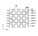
- FIG. 3 to 6 show patterns of the protrusions 140 of the light extraction layer 120 used in the simulation. These drawings are schematic top views when the light extraction layer 120 is viewed from above.
- a regular quadrangular pyramid is assumed as the shape of each projection 140, and in each projection 140, the intersection of two straight lines is the top point of the regular quadrangular pyramid.
- the regular quadrangular pyramid-shaped protrusions 140 are arranged along the X direction at different Y coordinates (Y1, Y2, Y3). That is, the repeated row 130X1 is formed at the Y1 coordinate, the repeated row 130X2 is formed at the Y2 coordinate, and the repeated row 130X3 is formed at the Y3 coordinate. Note that a region where the protrusion 140 is not provided forms a substantially flat horizontal region 143.
- the interval Py in the Y direction between the repeated rows 130X is not particularly limited. In the example of FIG. 3, the interval Py is equal to the length of one bottom side of the protrusion 140. In addition, each space
- a repeated row 130X ′ (130X′1 to 130X′3) is arranged instead of the repeated row 130X in FIG.
- the repeated row 130X ′ is configured by disposing the protrusions 140 discontinuously along the X direction.
- the protrusions 140 are spaced apart from each other by a distance Px.
- the interval Px may be equal to or different from the interval Py. Further, the intervals Px may be equal or different.
- the periodic pattern 150D in FIG. 6 is obtained by removing the protrusions 140 in a checkered pattern from the periodic pattern 150C in FIG. 5, and a horizontal region 143 is formed in a portion without the protrusions 140.
- This periodic pattern 150D can also be regarded as a configuration in which repeated rows 130X ′′ 1 and repeated rows 130X ′′ 2 are alternately arranged along the Y direction.
- the repeated rows 130X ′′ are not separated in the Y direction, but the repeated rows 130X ′′ may be spaced apart by an interval Py in the Y direction.
- each protrusion 140 In the above periodic pattern, a regular quadrangular pyramid was assumed as the shape of each protrusion 140. However, the shape of each protrusion 140 is not limited to this, and the protrusion 140 may have any shape as long as it is a pyramid (for example, a triangular pyramid, a quadrangular pyramid, a hexagonal pyramid, etc.).
- each protrusion 140 has the same base dimension in the X direction and the Y direction (that is, a regular quadrangular pyramid is assumed). However, each protrusion 140 may have different base dimensions in the X direction and the Y direction.
- each protrusion 140 may have a triangular prism shape having a longitudinal axis along one direction.
- a pattern is formed by arranging the protrusions 149 having apex sides 146 extending along the Y direction along the X direction.
- the angle ⁇ formed by the base of the triangle obtained in the cross section perpendicular to the top side 146 of the protrusion 149 and the other side is set in the range of 5 ° to 70 °, thereby achieving the effect of the present invention. Obtainable.
- the example of FIG. 2B is a case where the bottom side constituting the protrusion 140 of the light extraction layer 120 is in the range of 0.1 to 100 ⁇ m.
- the protrusions 140 and 149 are randomly arranged on the XY plane.
- the pattern of the light extraction layer 120 may be configured such that the substantially pyramid-shaped protrusions 140 as shown in FIGS. 3 to 6 and the substantially triangular prism-shaped protrusions as shown in FIG. good. Further, these protrusions 140 and 149 may have different shapes.
- the configuration of the present invention has been described by taking as an example the case where the protrusion 140 has a pyramid shape having a top point or the protrusion 149 has a triangular prism shape having a top side.
- the shape of the protrusions 140 and 149 may be substantially a truncated pyramid.
- the top point (or the top side) can be obtained by extrapolating the sides forming the side surfaces of the truncated pyramid and obtaining the intersections thereof.
- the inclination angle ⁇ can be obtained by assuming a vertical section passing through this virtual top point or a section perpendicular to the top side.
- each member included in the organic EL element (Each member included in the organic EL element) Next, each member which comprises the organic EL element by this invention is demonstrated.
- the support substrate 110 is made of a transparent material, that is, a material having a high transmittance for visible light.
- the support substrate 110 may be, for example, a glass substrate or a plastic substrate.
- the material of the glass substrate includes inorganic glass such as alkali glass, non-alkali glass or quartz glass.
- the plastic substrate material include polyester, polycarbonate, polyether, polysulfone, polyethersulfone, polyvinyl alcohol, and fluorine-containing polymers such as polyvinylidene fluoride and polyvinyl fluoride.
- the thickness of the support substrate 110 is not particularly limited, but may be in the range of 0.1 mm to 2.0 mm, for example. Considering strength and weight, the thickness of the support substrate 110 is preferably 0.5 mm to 1.4 mm.
- Light extraction layer 120 As described above, composed of a glass material having a high refractive index (range of the refractive index n d 1.6 to 2.2). Examples of such a glass material include soda lime glass, borosilicate glass, alkali-free glass, and quartz glass.
- a plurality of scattering materials may be dispersed in this glass material.
- the scattering material is composed of, for example, bubbles, precipitated crystals, glass material particles different from the glass material serving as a matrix, phase separation glass, and the like.
- a phase-separated glass refers to a glass composed of two or more types of glass phases. A larger difference between the refractive index of the glass material serving as the matrix and the refractive index of the scattering material is better.
- the amount of the scattering material in the light extraction layer 120 may decrease from the inside of the light extraction layer 120 to the outside, and in this case, highly efficient light extraction can be realized.
- the thickness of the light extraction layer 120 is, for example, in the range of 5 ⁇ m to 50 ⁇ m.
- the fact that the light extraction layer does not substantially contain a scattering material means that no scattering material is intentionally formed in the light extraction layer. Therefore, when the light extraction layer is formed of a glass material, it goes without saying that bubbles, crystals, and the like that are naturally formed when the light extraction layer itself is formed may be included.
- the first electrode 170 is required to have a translucency of 80% or more in order to extract light generated in the organic light emitting layer 180 to the outside. Also, a high work function is required to inject many holes.
- the first electrode 170 includes, for example, ITO, SnO 2 , ZnO, IZO (Indium Zinc Oxide), AZO (ZnO—Al 2 O 3 : zinc oxide doped with aluminum), GZO (ZnO—Ga 2 O). 3 : zinc oxide doped with gallium), Nb-doped TiO 2 , and Ta-doped TiO 2 .
- the thickness of the first electrode 170 is usually about 50 nm to 1.0 ⁇ m.
- the refractive index of the first electrode 170 is in the range of 1.9 to 2.2.
- the refractive index of the first electrode 170 can be decreased by increasing the carrier concentration.
- Commercially available ITO contains 10 wt% SnO 2 as standard, but the refractive index of ITO can be lowered by further increasing the Sn concentration.
- the carrier concentration increases, but the mobility and transmittance decrease. Therefore, it is necessary to determine the Sn amount in consideration of the overall balance.
- the organic light emitting layer 180 is a layer having a light emitting function, and is usually composed of a hole injection layer, a hole transport layer, a light emitting layer, an electron transport layer, and an electron injection layer. However, it is obvious to those skilled in the art that the organic light emitting layer 180 does not necessarily have all of the other layers as long as it has a light emitting layer. In general, the refractive index of the organic light emitting layer 140 is in the range of 1.7 to 1.8.
- the hole injection layer preferably has a small difference in ionization potential in order to lower the hole injection barrier from the first electrode 170.
- the charge injection efficiency from the electrode to the hole injection layer is increased, the drive voltage of the organic EL element 100 is lowered and the charge injection efficiency is increased.
- the material of the hole injection layer a high molecular material or a low molecular material is used.
- polymer materials polyethylene dioxythiophene (PEDOT: PSS) doped with polystyrene sulfonic acid (PSS) is often used, and among low molecular materials, phthalocyanine-based copper phthalocyanine (CuPc) is widely used.
- the hole transport layer serves to transport holes injected from the hole injection layer to the light emitting layer.
- Examples of the hole transport layer include triphenylamine derivatives, N, N′-bis (1-naphthyl) -N, N′-diphenyl-1,1′-biphenyl-4,4′-diamine (NPD), N , N′-Diphenyl-N, N′-bis [N-phenyl-N- (2-naphthyl) -4′-aminobiphenyl-4-yl] -1,1′-biphenyl-4,4′-diamine ( NPTE), 1,1′-bis [(di-4-tolylamino) phenyl] cyclohexane (HTM2), and N, N′-diphenyl-N, N′-bis (3-methylphenyl) -1,1′- Diphenyl-4,4′-diamine (TPD) or the like is used.
- NPD triphenylamine derivatives
- the thickness of the hole transport layer is, for example, in the range of 10 nm to 150 nm.
- the thickness is usually in the range of 10 nm to 150 nm because of the problem of short circuit between electrodes.
- the light emitting layer has a role of providing a field where the injected electrons and holes are recombined.
- the organic light emitting material a low molecular weight or high molecular weight material is used.
- Examples of the light emitting layer include tris (8-quinolinolato) aluminum complex (Alq3), bis (8-hydroxy) quinaldine aluminum phenoxide (Alq′2OPh), bis (8-hydroxy) quinaldine aluminum-2,5- Dimethylphenoxide (BAlq), mono (2,2,6,6-tetramethyl-3,5-heptanedionate) lithium complex (Liq), mono (8-quinolinolato) sodium complex (Naq), mono (2, 2,6,6-tetramethyl-3,5-heptanedionate) lithium complex, mono (2,2,6,6-tetramethyl-3,5-heptanedionate) sodium complex and bis (8-quinolinolate) Metal complexes of quinoline derivatives such as calcium complexes (Caq2), tetraphenylbutadiene, pheny Quinacridone (QD), anthracene, perylene, as well as fluorescent substance such as coronene.
- a quinolinolate complex may be used, and in particular, an aluminum complex having 8-quinolinol and a derivative thereof as a ligand may be used.
- the electron transport layer serves to transport electrons injected from the electrode.
- the electron transport layer include quinolinol aluminum complex (Alq3), oxadiazole derivatives (for example, 2,5-bis (1-naphthyl) -1,3,4-oxadiazole (END), and 2- ( 4-t-butylphenyl) -5- (4-biphenyl))-1,3,4-oxadiazole (PBD) etc.), triazole derivatives, bathophenanthroline derivatives, silole derivatives and the like.
- the electron injection layer is configured, for example, by providing a layer doped with an alkali metal such as lithium (Li) or cesium (Cs) at the interface with the second electrode 190.
- the second electrode 190 a metal having a small work function or an alloy thereof is used.
- the second electrode 190 may be, for example, an alkali metal, an alkaline earth metal, a metal belonging to Group 3 of the periodic table, or the like.
- aluminum (Al), magnesium (Mg), or an alloy thereof is used for the second electrode 190.
- a laminated electrode in which aluminum (Al) is deposited on a thin film of aluminum (Al), magnesium silver (MgAg), lithium fluoride (LiF), or lithium oxide (Li 2 O) may be used. good.
- a laminated film of calcium (Ca) or barium (Ba) and aluminum (Al) may be used.
- Simulation 1 The effect of the surface shape of the light extraction layer on the light extraction efficiency of the organic EL element was evaluated by computer simulation.
- ray tracing software Light Tools: manufactured by Cybernet System
- the following modeling was performed during the simulation.
- the organic EL element is configured as shown in FIG. That is, the organic EL element 800 includes a first layer 810 (refractive index 1.55), a second layer 825 (refractive index 1.9), a third layer 885 (refractive index 1.9), and a fourth layer.
- the four-layer structure of the layer 890 of FIG. In comparison with FIG. 2A, the first layer 810 corresponds to the support substrate 110, and the second layer 825 corresponds to the light extraction layer 120 + the first electrode 170 + the lower half of the organic light emitting layer 180.
- the third layer 885 corresponds to the upper half of the organic light emitting layer 180, and the fourth layer 890 corresponds to the second electrode 190.
- the interface between the second layer 825 and the third layer 885 is a light emitting surface, and the fourth layer 890 is a reflecting surface (reflectance 80%, absorption 20%). These surfaces are assumed to have a thickness of zero.
- the thickness of the first layer 810 is 550 ⁇ m
- the thickness of the third layer 885 is 0.03 ⁇ m.
- the film thickness of the second layer 825 is expressed by the sum of 10.25 ⁇ m of the basic portion up to the bottom surface of the protrusion 840 and the height of the protrusion 840.
- the height of the protrusion 840 varies depending on the angle ⁇ of the apex point 845.
- the length of the bottom side of the protrusion 840 is constant at 100 ⁇ m even if the angle ⁇ of the top point 845 changes.
- the protrusion 840 has a regular quadrangular pyramid shape, and the pattern of the protrusion 840 has the form shown in FIG.
- the protrusion 840 has a regular quadrangular pyramid shape because the substantially triangular shape obtained in the vertical cross section passing through the top point of the protrusion is an isosceles triangle, and the two angles formed by the base and other sides are the same angle. This is because the relationship between the light extraction amount and the light extraction amount can be simplified. Actually, the two angles formed by the base and the other sides may be different. In that case, the light extraction amount is determined by the ratio of the respective angles and the lengths of the corresponding sides. it is obvious.
- the inclination angle is a triangle of 30 ° and 60 °
- the ratio of the lengths of the corresponding sides is 1: ⁇ 3
- the light extraction amount in the case of an isosceles triangle having an inclination angle of 30 ° is here.
- the light extraction amount B in the case of an isosceles triangle with an inclination angle of 60 ° is calculated by (A + ⁇ 3B) / (1 + ⁇ 3).
- the first layer 810 The amount of light OP (light extraction amount) extracted from the lower side was calculated.
- the total number of light rays emitted was 100,000.
- FIG. 9 shows the relationship between the inclination angle ⁇ of the protrusion 840 of the second layer 825 and the light extraction amount obtained by simulation.
- the vertical axis indicates the light extraction amount OP, normalized with the light extraction amount OP 0 when the inclination angle ⁇ is 0 ° (that is, no projection) as a reference (1.0).
- the inclination angle ⁇ is 5 ° to 70 °
- the light extraction amount (standardized value) exceeds 1.1, and a good light extraction effect can be obtained.
- the inclination angle ⁇ is 15 ° to 40 °
- the light extraction amount (standardized value) exceeds 1.5
- the light extraction amount OP is larger than that in the case where the scattering layer has no protrusion. It was found to increase 1.5 times.
- FIG. 10 shows the result of the same simulation performed when the second layer 825 includes a scattering material (refractive index of 1.0) having a radius of 0.5 ⁇ m.
- FIG. 10 also shows the result of FIG. 9 described above (that is, the case where the second layer 825 does not include a scattering material).
- the vertical axis shows the light extraction amount OP normalized with reference to the case where the second layer 825 has no protrusions and does not contain a scattering material (that is, the above-described light extraction amount is OP 0 ).
- the amount of scattering material added was three types: 1.0 ⁇ 10 5 pieces / mm 3 , 1.0 ⁇ 10 6 pieces / mm 3 , and 1.0 ⁇ 10 7 pieces / mm 3 . It is assumed that the scattering material is dispersed throughout the second layer 825.
- the amount of light extraction is generally improved by adding a scattering material to the second layer 825.
- the amount of the scattering material added is 1.0 ⁇ 10 6 particles / mm 3 or less, the effect is not significant. Therefore, it can be said that it is necessary to add about 1.0 ⁇ 10 7 particles / mm 3 of the scattering material when further improving the light extraction amount by adding the scattering material.
- the light extraction amount of the organic EL element is significantly improved by providing protrusions on the surface of the light extraction layer and setting the inclination angle ⁇ in the range of 5 ° to 70 °.
- the height of the protrusion 840 is not changed here, and is constant at 50 ⁇ m.
- the light extraction amount obtained by the simulation was calculated by normalizing with the value in the case where the protrusion 840 was not present on the surface of the second layer 825.
- the light extraction amount (standardized value) was 1.41. From this result, even when the surface of the light extraction layer has a periodic pattern of protrusions as shown in FIG. 7, the amount of light extraction from the organic EL element is significantly improved as compared with the case without the periodic pattern. It was shown that.
- the periodic pattern 150C (case 1) shown in FIG. 5 described above, the periodic pattern 150B (case 2 and case 3) shown in FIG. 4 described above, and the periodic pattern shown in FIG. 150A (case 4, case 6, case 7) and the periodic pattern 150D (case 5) shown in FIG. 6 described above were employed.
- the height of the protrusion 840 was fixed at 50 ⁇ m in all cases. Further, the inclination angle ⁇ of the protrusion 840 is constant at 30 ° (that is, the apex angle ⁇ is constant at 120 °). Further, the base of the protrusion 840 was constant at 173.2 ⁇ m in both the X direction and the Y direction.
- the horizontal axis indicates the ratio of the area of the horizontal region on the surface of the scattering layer to the entire area.
- the vertical axis indicates the light extraction amount obtained by simulation. However, as described above, this value was calculated by normalizing with the value when there is no protrusion 840 on the surface of the second layer 825. From this result, it was found that the amount of light extraction tends to increase as the horizontal region where the protrusion 840 does not exist decreases.
- the same simulation is performed for the case where the second layer 825 further includes a scattering material (refractive index 1.0) having a radius of 0.5 ⁇ m.
- the results are shown in FIG. 12 and FIG. 12 shows a case where the inclination angle is 30 °, and FIG. 13 shows a case where the inclination angle is 5 °.
- the horizontal axis represents the ratio of the area of the horizontal region on the surface of the scattering layer to the total area.
- the vertical axis indicates the light extraction amount obtained by simulation, and the value obtained when there is no projection 840 on the surface of the second layer 825 and no scattering material is used as a reference, as in FIG. It is standardized.
- the amount of the scattering material added was three types: 1.0 ⁇ 10 5 pieces / mm 3 , 1.0 ⁇ 10 6 pieces / mm 3 , and 1.0 ⁇ 10 7 pieces / mm 3 . It is assumed that the scattering material is dispersed throughout the second layer 825. From FIG. 12 and FIG. 13, the light extraction amount is improved by adding the scattering material, and it is possible to increase the light extraction amount by adding the scattering material even if the proportion of the horizontal region is large. I understand that.
- the light extraction efficiency can be improved without containing a large amount of scattering substances in the light extraction layer.
- the amount of light scattered not only forward but also backward increases.
- the front indicates the direction of the light extraction substrate as viewed from the light emitting layer
- the rear indicates the direction opposite to the light extraction substrate as viewed from the light emission layer.
- the light scattered backward is reflected by the metal surface when a metal material is used as the cathode, and can be taken out by changing the traveling direction forward.
- the reflectance on the metal surface is not 100%, the amount of light always decreases. For example, in Al often used as a cathode, the reflectance is about 80%, and about 20% of light is lost.
- the light extraction layer and the transparent electrode absorb light slightly.
- the light extraction efficiency can be improved by providing the surface of the light extraction layer with an inclination without increasing the content of the scattering material.
- the present invention can be applied to an organic EL element used for a light emitting device or the like.
Landscapes
- Physics & Mathematics (AREA)
- Optics & Photonics (AREA)
- General Physics & Mathematics (AREA)
- Electroluminescent Light Sources (AREA)
Abstract
透光性基板は、透明支持基板と、該透明支持基板上に形成され、D線において1.6~2.2の範囲である第1の屈折率を有するガラス材料と、D線において前記第1の屈折率とは異なる第2の屈折率を有する散乱物質とを有する光取り出し層とを備え、前記光取り出し層の表面には、一つの頂点を有する略角錐状の突起、または一つの頂上辺を有する略三角柱状の突起が形成されており、前記突起の前記頂上点を通る垂直な断面、または前記突起の前記頂上辺に対して垂直な断面において得られた略三角形の底辺とその他の辺とのなす角度のうち少なくとも一つの角度φが、10°~60°の範囲である。
Description
本発明は、有機EL素子に関する。
有機エレクトロルミネッセンス(有機EL)素子は、ディスプレイ、バックライト、および照明用途等に広く用いられている。
一般的な有機EL素子は、支持基板上に設置された第1の電極(陽極)と、第2の電極(陰極)と、これらの電極間に設置された有機発光層とを有する。電極間に電圧を印加すると、それぞれの電極から、有機発光層にホールおよび電子が注入される。このホールと電子が有機発光層内で再結合された際に、結合エネルギーが生じ、この結合エネルギーによって有機発光層中の発光材料が励起される。励起した発光材料が基底状態に戻る際に発光が生じるため、これを利用することにより、発光(EL)素子が得られる。
通常、第1の電極、すなわち陽極には、ITO(Indium Tin Oxide)のような透明薄膜が使用され、第2の電極、すなわち陰極には、アルミニウムおよび銀等の金属薄膜が使用される。
最近では、第1の電極と支持基板の間に、樹脂製の光取り出し層を設置することが提案されている。例えば、第1の電極と支持基板の間に、周期的な凹凸を有する樹脂製の光取り出し層を設置することにより、有機層で生じた光の外部取り出し効率を高めることができることが開示されている(特許文献1)。
また、光取り出し層内に散乱物質を付与することで光取り出し効率を向上させる方法が開示されている(特許文献2)。
しかしながら、光取り出し層を樹脂で構成した場合、以下のような問題が生じ得る。
(1)光取り出し層に使用される樹脂は、通常の場合、吸湿性を有する。このため、樹脂製光取り出し層を長時間使用した場合、光取り出し層が劣化したり、着色したりするおそれがある。光取り出し層にこのような劣化や着色が生じると、有機EL素子の発光効率が低下してしまう。
(2)光取り出し層は、通常の場合、高い屈折率を有する必要がある。これは、陽極(ITO(インジウムスズ酸化物)電極)の屈折率が比較的高いため、屈折率が低い光取り出し層を使用した場合、両者の界面で全反射が生じてしまう可能性が高くなるからである。しかしながら、樹脂では、そのような高屈折率の光取り出し層を形成することは難しい。
このように、従来の樹脂製の光取り出し層には、耐環境性および屈折率の点で問題がある。
また、前述の特許文献1では、周期的な凹凸を有する樹脂製の光取り出し層が使用される。しかしながら、この文献では、凹凸形状の最適なパターンが十分に開示されているとは言い難く、具体的にどのような凹凸形状パターンを有する光取り出し層であれば、十分な光取り出し効率が得られるのか不明な点が多い。
また、前述の特許文献2のように散乱物質を含有しても、光取り出し効率の向上のために、含有できる量には限界がある。
本発明は、このような課題に鑑みなされたものであり、本発明では、良好な耐環境性および高い屈折率を有する光取り出し層を備え、かつ光取り出し効率の良好な有機EL素子を提供することを目的とする。また、そのような有機EL素子に使用され得る透光性基板を提供することを目的とする。
本発明の第1の態様の透光性基板は、透明支持基板と、該透明支持基板上に形成され、D線において1.6~2.2の範囲である第1の屈折率を有するガラス材料と、D線において前記第1の屈折率とは異なる第2の屈折率を有する散乱物質とを有する光取り出し層とを備え、前記光取り出し層の表面には、一つの頂点を有する略角錐状の突起、または一つの頂上辺を有する略三角柱状の突起が形成されており、前記突起の前記頂上点を通る垂直な断面、または前記突起の前記頂上辺に対して垂直な断面において得られた略三角形の底辺とその他の辺とのなす角度のうち少なくとも一つの角度φが、10゜~60゜の範囲である。
本発明の第2の態様の透光性基板は、透明支持基板と、該透明支持基板上に形成され、D線において1.6~2.2の範囲である第1の屈折率を有するガラス材料を有し、かつ、前記第1の屈折率とは異なる第2の屈折率を有する散乱物質を実質的に含有しない光取り出し層とを備え、前記光取り出し層の表面には、一つの頂上点を有する略角錐状の突起、または一つの頂上辺を有する略三角柱状の突起が形成されており、前記突起の頂上点を通る垂直な断面、または前記突起の頂上辺に対して垂直な断面において得られた略三角形の底辺とその他の辺とのなす角度のうち少なくとも一つの角度φが、5゜~70゜の範囲である。
また、本発明の透光性基板において、前記散乱物質は、気泡および前記ガラス材料の少なくとも一方を構成するガラスの析出結晶であっても良い。
また、本発明の透光性基板において、前記角度φは、15゜~40゜の範囲であっても良い。
また、本発明の透光性基板において、前記底辺の寸法が0.1μm~100μmの範囲内の場合、前記突起は周期的に配列されていなくても良い。
また、本発明の透光性基板において、前記底辺の寸法が0.1μm~100μmの範囲外の場合、前記突起は周期的に配列されても良い。
また、本発明の有機EL素子は、上述した透光性基板と、該光取り出し層上に形成された第1の電極と、該第1の電極上に形成された有機発光層と、該有機発光層上に形成された第2の電極とを有する。
本発明では、良好な耐環境性および高い屈折率を有する光取り出し層を備え、かつ光取り出し効率の良好な有機EL素子を提供することができる。また、そのような有機EL素子に使用され得る透光性基板を提供することができる。
以下、図面を参照して、本発明について説明する。
まず、本発明の特徴をより良く理解するため、図1を用いて、従来の有機EL素子の構成について簡単に説明する。
図1には、従来の有機EL素子の簡略的な断面図を示す。
図1に示すように、従来の有機EL素子1は、透光性基板5と、第1の電極(陽極)70と、有機発光層80と、第2の電極(陰極)90とをこの順に積層することにより構成される。透光性基板5は、支持基板10上に光取り出し層20を積層することにより構成される。なお、図1の例では、有機EL素子1の下側の表面(すなわち支持基板10の露出面)が光取り出し面60となる。
光取り出し層20は、入射する光を複数の方向に散乱する役割を有する。従って、光取り出し層20を有する有機EL素子1では、光取り出し層80から放射された光の減衰を抑制することができ、光取り出し層20を有さない構成に比べて、光取り出し面60から出射される光量を向上させることができる。
ここで、従来の有機EL素子1では、光取り出し層20は、樹脂で構成される。
しかしながら、樹脂で構成された光取り出し層20には、以下のような問題が生じ得る。
(1)光取り出し層20に使用される樹脂は、通常の場合、吸湿性を有する。このため、光取り出し層20を長時間使用した場合、光取り出し層20が劣化したり、着色したりするおそれがある。光取り出し層20にこのような劣化や着色が生じると、有機EL素子1の発光効率が低下してしまう。
(2)光取り出し層20には、通常の場合、高い屈折率を有することが望まれる。これは、第1の電極(通常、ITO(インジウムスズ酸化物)電極)の屈折率が比較的高いため、屈折率が低い光取り出し層を使用した場合、両者の界面で全反射が生じてしまう可能性が高くなるからである。しかしながら、樹脂では、そのような高屈折率の光取り出し層を形成することは難しい(通常の場合、樹脂の屈折率ndは、1.4~1.6程度)。
このように、従来の樹脂製の光取り出し層20には、耐環境性および屈折率の点で問題がある。
これに対して、本発明では、一つの特徴として、光取り出し層が比較的高い屈折率を有するガラスで構成されているという特徴を有する。
ガラスは、樹脂に比べて耐環境性に優れるため、長時間使用しても劣化が生じ難い。また、本発明において光取り出し層に使用されるガラスは、屈折率ndが1.6~2.2の範囲にある。このような高い屈折率を有する光取り出し層を使用した場合、光取り出し層と第1の電極との界面で、光が反射してしまうという問題が軽減される。
さらに、本発明では、別の特徴として、光取り出し層の表面に、略角錐状の突起、または略三角柱状の突起による周期パターンが形成されているという特徴を有する。
以降に示すように、このような光取り出し層を備える有機EL素子では、より高い光の外部取り出し効率を達成することができる。
なお、前述の特許文献1には、樹脂製の光取り出し層に凹凸構造を形成することが開示されている。しかしながら、この文献では、凹凸形状の最適なパターンが十分に開示されているとは言い難く、具体的にどのような凹凸形状パターンを有する光取り出し層であれば、十分な光取り出し効率が得られるのかは不明である。
これに対して、本願発明者らは、以降に示すように、様々なパターンについて考察を繰り返し、光取り出し層の表面が以下の形態を有する場合に、良好な光取り出し効率が得られることを初めて見出した:
(i)光取り出し層の表面が、一つの「頂上点」を有する略角錐状の突起による周期パターンを有し、「傾斜角」が、5゜~70゜の範囲にある場合。
(i)光取り出し層の表面が、一つの「頂上点」を有する略角錐状の突起による周期パターンを有し、「傾斜角」が、5゜~70゜の範囲にある場合。
ここで、本願において、「頂上点」という用語は、角錐に含まれる各頂点のうち、光取り出し層と支持基板の界面(以下、単に「界面」と称する)から最も遠い距離にある頂点を意味する。例えば、三角錐以外の角錐の場合、「頂上点」からは、最も多くの辺が延びることになる(ただし、三角錐の場合、各頂点から延びる辺の数は、いずれも3である)。
また、「傾斜角」と言う用語は、突起の「頂上点」を通る垂直な断面において得られた略三角形の「頂上点」を通る辺と、底辺のなす角(2つ存在する)を意味する。ここで、略三角形とは、すべての頂角が鋭角となっているものだけを含むことを意図するのではなく、製造プロセスにおいて頂点が丸み帯びているものを含むことを意図する。
(ii)光取り出し層の表面が、一つの「頂上辺」を有する略三角柱状の突起による周期パターンを有し、「傾斜角」が、5゜~70゜の範囲にある場合。
ここで、本願において、「頂上辺」という用語は、略三角柱に含まれる軸方向に延びる各辺のうち、「界面」から最も遠い距離にある辺を意味する。
また、この場合、「傾斜角」は、突起の「頂上辺」を通る垂直な断面において得られた略三角形の頂点を通る辺と、底辺のなす角(2つ存在する)のうちの大きい方を意味する。
すなわち、本発明は、光取り出し層の表面に、一つの頂上点を有する略角錐状の突起による周期もしくは非周期パターン、または一つの頂上辺を有する略三角柱状の突起による周期もしくは非周期パターンが形成されており、前記突起の前記頂上点を通る垂直な断面、または前記突起の前記頂上辺に対して垂直な断面において得られた略三角形の底辺とその他の辺とのなす角度のうちの少なくとも一つの角度が、5゜~70゜の範囲であることを特徴とするものである。
このような光取り出し層の構成により、本発明による有機EL素子では、良好な耐環境性が得られるとともに、従来に比べて有意な光取り出し効率を得ることが可能となる。
なお、以上の説明では、頂上点または頂上辺が明確に認められる突起の場合を例に、「傾斜角」を定義した。
しかしながら、例えば、突起を構成する各辺または各面が非直線的にまたは曲面的に形成されており、突起の頂上点または頂上辺が不明瞭な場合も、以下のようにして「傾斜角」を求めることができる。すなわち、(i)の場合、突起の「頂上点」は、突起の複数の稜線を直線外挿し、その交点を求めることにより定めることができる。また、傾斜角は、このようにして定められた「頂上点」を通る垂直な断面において得られた略三角形をもとに、(必要なら、得られた略三角形の「頂上点」を通る辺を直線的に外挿して)定めることができる。同様に、(ii)の場合、突起の「頂上辺」は、突起の傾斜面を直線外挿し、その交点を求めることにより定めることができる。また、傾斜角は、このようにして定められた「頂上辺」を通る垂直な断面において得られた略三角形をもとに、(必要なら、得られた略三角形の頂点を通る傾斜面を直線的に外挿して)定めることができる。
(本発明による有機EL素子の構成)
以下、図2を参照して、本発明の構成について詳しく説明する。
以下、図2を参照して、本発明の構成について詳しく説明する。
図2には、本発明による有機EL素子の概略的な部分断面図の一例を示す。図2(A)は、光取り出し層の突起が周期性を有する場合を示す部分断面図であり、図2(B)は、光取り出し層の突起が周期性を有さない(ランダムな)場合を示す部分断面図である。以下において詳細に説明するが、突起を構成する底辺寸法が0.1μm~100μmの範囲内である場合は、図2(B)の構成が好ましく、突起を構成する底辺寸法が0.1μm~100μmの範囲外である場合は、図2(A)の構成であっても良い。発明者らの知見によると、底辺寸法が0.1μm~100μmの範囲内の場合、突起の配置に周期性があると、光が回折および干渉する可能性があるため、例えば白色有機EL素子では光が虹色に見えるといった問題が生じる場合がある。そのため、底辺寸法が0.1μm~100μmの範囲内の場合は、突起の配置に周期性がない方が好ましい。ただし、光取り出し層内に散乱物質が分散されている場合、および、有機EL素子外側に散乱性を有するフィルム等を付与する場合には、光の回折や干渉の効果が低減する効果があるため、突起が周期的に配列されていても良い。一方、底辺寸法が0.1μm~100μmの範囲外の場合、突起の配置に周期性があっても光の干渉が生じないため、突起の配置は、ランダムまたは周期性のいずれでも良い。
図2に示すように、本発明による有機EL素子100は、透光性基板105と、第1の電極(陽極)170と、有機発光層180と、第2の電極(陰極)190とを、この順に積層することにより構成される。図2A、図2Bの例では、有機EL素子100の下側の表面(すなわち透光性基板105の露出面)が光取り出し面160となる。
第1の電極170は、例えばITO(インジウムスズ酸化物)のような透明金属酸化物薄膜で構成される。一方、第2の電極190は、例えばアルミニウムや銀のような金属で構成される。本発明において、第1及び第2の電極は、上述した材質に限定されるのではなく、他の材質で構成されていても良いことは言うまでもない。
また、有機発光層180は、通常の場合、発光層の他、電子輸送層、電子注入層、ホール輸送層、ホール注入層など、複数の層で構成される。
透光性基板105は、透明な支持基板110と、その上部の光取り出し層120とで構成される。光取り出し層120は、入射光を散乱させ、光取り出し層120に隣接する層との界面での光の反射を軽減する役割を有する。
ここで、本発明では、前述のように、光取り出し層120は、屈折率ndが1.6~2.2の範囲にあるガラス材料で構成される。また、光取り出し層120の表面には、一つの頂上点145を有する略角錐状の突起140による周期パターンまたは非周期パターンが形成されている。また、光取り出し層に用いるガラス材料の屈折率ndは1.7~2.2の範囲であっても良い。なお、本文中でのndとはd線(587.56nm)での屈折率を示している。
図2において、突起140の傾斜角φ(すなわち、突起140の頂上点145を通る垂直な断面において得られた略三角形の、頂上点145を通る辺と、底辺のなす角度)は、5゜~70゜の範囲であり、特に5゜~60゜の範囲であることが好ましく、15゜~40゜の範囲であることがさらに好ましい。これにより、良好な光取り出し効率を得ることができる。
また、突起140の底辺寸法は、0.1μm~100μmの範囲内である場合、突起140の配置はランダムであることが好ましい。ただし、光取り出し層内に散乱物質が分散されている場合、および、有機EL素子外側に散乱性を有するフィルム等を付与する場合には、光の回折や干渉の効果が低減する効果があるため、突起が周期的に配列されていても良い。なお、突起140の底辺寸法が0.1μm~100μmの範囲外である場合、突起140の配置は周期的であっても良い。
なお、図2の例では、光取り出し層120の上部に積層される各部材、すなわち、第1の電極170、有機発光層180、および第2の電極190は、いずれも、光取り出し層120の表面パターンに対応した表面形状を有する。例えば、本有機EL素子100を上部から見た場合、第2の電極190は、凹凸形状となっている。
図2Aの例は、光取り出し層120の突起140を構成する底辺が0.1μm~100μmの範囲外の場合である。この場合、光取り出し層120のパターンは、断面が略三角形状の突起140が、X方向に沿って繰り返されることにより構成された繰り返し行130Xを有する。このような繰り返し行130Xは、Y方向の異なる座標(例えば、Y1,Y2,...)においても、同様に配置されても良い。換言すれば、繰り返し行130Xは、XY二次元平面において、複数配置されても良い(例えば図3参照)。
また、この他にも、光取り出し層120のパターンとして、様々な態様が考えられる。
図3乃至図6には、シミュレーションで用いた光取り出し層120の突起140のパターンを示す。これらの図は、光取り出し層120を上方から見たときの概略的な上面図である。また、各突起140の形状として、正四角錐を想定しており、各突起140において、2本の直線の交点が正四角錐の頂上点となる。
図3の周期パターン150Aの場合、正四角錐状の各突起140は、異なるY座標(Y1、Y2、Y3)において、X方向に沿って配置される。すなわち、Y1座標において、繰り返し行130X1が形成され、Y2座標において、繰り返し行130X2が形成され、Y3座標において、繰り返し行130X3が形成されている。なお、突起140が設置されていない領域は、略平坦な水平領域143を形成する。
各繰り返し行130X同士のY方向の間隔Pyは、特に限られず、図3の例では、間隔Pyは、突起140の一つの底辺の長さと等しくなっている。なお、それぞれの間隔Py(例えばY1とY2の間隔と、Y2とY3の間隔)は、等しくても、異なっていても良い。
一方、図4の周期パターン150Bの場合、図3における繰り返し行130Xの代わりに、繰り返し行130X’(130X’1~130X’3)が配置されている。ここで、繰り返し行130X’は、突起140がX方向に沿って不連続に配置されて構成される。例えば、図4の例では、各繰り返し行130X’において、突起140は、相互に間隔Pxだけ離間して配置されている。間隔Pxは、間隔Pyと等しくても、異なっていても良い。また、それぞれの間隔Pxは、等しくても、異なっていても良い。
また、図5の周期パターン150Cでは、図3における繰り返し行130Xが、Y方向において、離間せずに(水平領域143が生じないように)繰り返し配置されている。すなわち、図5の周期パターン150Cは、図3の周期パターン150Aにおいて、間隔Px=0としたものである。
さらに、図6の周期パターン150Dは、図5における周期パターン150Cにおいて、突起140を市松模様状に取り除いたものであり、突起140のない部分には、水平領域143が形成される。
この周期パターン150Dは、繰り返し行130X”1と、繰り返し行130X”2をY方向に沿って交互に配置した構成とも見なすことができる。なお、図6では、各繰り返し行130X”は、Y方向において離間されていないが、各繰り返し行130X”は、Y方向において間隔Pyだけ離して配置されても良い。
なお、以上の周期パターンでは、各突起140の形状として、正四角錐を想定した。しかしながら、各突起140の形状は、これに限られず、突起140は、角錐状であれば、いかなる形状であっても良い(例えば、三角錐、四角錐、六角錐等)。
また、以上の例では、各突起140は、X方向およびY方向において、同じ底辺寸法を有する(すなわち正四角錐を仮定した)。しかしながら、各突起140は、X方向およびY方向において、異なる底辺寸法を有しても良い。
あるいは、例えば、図7に示すように、各突起140は、一つの方向に沿った長手軸を有する三角柱状であっても良い。
図7に示す周期パターン150Eでは、Y方向に沿って延びる頂上辺146を有する各突起149がX方向に沿って配列されることにより、パターンが形成される。
この場合、突起149の頂上辺146に対して垂直な断面において得られた三角形の底辺とその他の辺とのなす角度φを、5゜~70゜の範囲にすることにより、本発明による効果を得ることができる。
この他にも、光取り出し層120のパターンとして、様々な態様が考えられることは、当業者には明らかである。
例えば、図2Bの例は、光取り出し層120の突起140を構成する底辺が0.1~100μmの範囲内の場合である。この場合、光取り出し層120のパターンは、突起140、149が、XY平面上にランダムに配置されている。例えば、光取り出し層120のパターンは、図3乃至図6に示したような略角錐状の突起140と、図7に示したような略三角柱状の突起が無秩序に配置されて構成されても良い。また、これらの突起140、149は、それぞれが異なった形状を有していても良い。
なお、以上の記載では、突起140が頂上点を有する角錐状、または突起149が頂上辺を有する三角柱状である場合を例に、本発明の構成を説明した。しかしながら、突起140、149の形状は、略角錐台状であっても良いことは当業者には明らかである。この場合、角錐台の側面を形成する辺を外挿して、それらの交点を求めることにより、頂上点(または頂上辺)を得ることができる。また、この仮想の頂上点を通る垂直断面、または頂上辺に垂直な断面を想定することにより、傾斜角φを得ることができる。
(有機EL素子に含まれる各部材)
次に、本発明による有機EL素子を構成する各部材について説明する。
次に、本発明による有機EL素子を構成する各部材について説明する。
(支持基板110)
支持基板110は、透明な材料、すなわち可視光に対する透過率が高い材料で構成される。支持基板110は、例えば、ガラス基板またはプラスチック基板であっても良い。
支持基板110は、透明な材料、すなわち可視光に対する透過率が高い材料で構成される。支持基板110は、例えば、ガラス基板またはプラスチック基板であっても良い。
ガラス基板の材料としては、アルカリガラス、無アルカリガラスまたは石英ガラスなどの無機ガラスが挙げられる。また、プラスチック基板の材料としては、ポリエステル、ポリカーボネート、ポリエーテル、ポリスルホン、ポリエーテルスルホン、ポリビニルアルコールならびにポリフッ化ビニリデンおよびポリフッ化ビニルなどのフッ素含有ポリマーが挙げられる。
支持基板110の厚さは、特に限られないが、例えば、0.1mm~2.0mmの範囲であっても良い。強度および重量を考慮すると、支持基板110の厚さは、0.5mm~1.4mmであることが好ましい。
(光取り出し層120)
光取り出し層120は、前述のように、高屈折率を有するガラス材料(屈折率ndが1.6~2.2の範囲)で構成される。そのようなガラス材料としては、例えば、ソーダライムガラス、ホウケイ酸塩ガラス、無アルカリガラス、および石英ガラスなどが挙げられる。
光取り出し層120は、前述のように、高屈折率を有するガラス材料(屈折率ndが1.6~2.2の範囲)で構成される。そのようなガラス材料としては、例えば、ソーダライムガラス、ホウケイ酸塩ガラス、無アルカリガラス、および石英ガラスなどが挙げられる。
また、このガラス材料中には、複数の散乱物質が分散されていても良い。散乱物質は、例えば、気泡、析出結晶、マトリックスとなるガラス材料とは異なるガラス材料粒子、分相ガラス等で構成される。分相ガラスとは、2種類以上のガラス相により構成されるガラスをいう。マトリックスとなるガラス材料の屈折率と、散乱物質の屈折率の差は、大きい方が良い。
また、光取り出し層120中の散乱物質の存在量は、光取り出し層120の内部から外側に向かって小さくなっていても良く、この場合、高効率の光取り出しを実現することができる。
光取り出し層120の厚さは、例えば5μm~50μmの範囲である。
ここで、光取り出し層において、散乱物質を実質的に含有しないとは、光取り出し層内に意図的に散乱物質を形成しないことを意味する。そのため、光取り出し層をガラス材料で形成する場合、光取り出し層そのものを形成するときに自然に形成されてしまう気泡や結晶等は含んでいても良いことは言うまでもない。
(第1の電極130)
第1の電極170には、有機発光層180で生じた光を外部に取り出すため、80%以上の透光性が要求される。また、多くの正孔を注入するため、仕事関数が高いことが要求される。
第1の電極170には、有機発光層180で生じた光を外部に取り出すため、80%以上の透光性が要求される。また、多くの正孔を注入するため、仕事関数が高いことが要求される。
第1の電極170には、例えば、ITO、SnO2、ZnO、IZO(Indium Zinc Oxide)、AZO(ZnO-Al2O3:アルミニウムがドーピングされた亜鉛酸化物)、GZO(ZnO-Ga2O3:ガリウムがドーピングされた亜鉛酸化物)、NbドープTiO2、およびTaドープTiO2などの材料が用いられる。
第1の電極170の厚さは、通常、50nm~1.0μm程度である。
第1の電極170の屈折率は、1.9~2.2の範囲である。例えば、第1の電極170としてITOを使用した場合、キャリア濃度を増加させることにより、第1の電極170の屈折率を低下させることができる。市販のITOでは、SnO2が10wt%含まれるものが標準となっているが、Sn濃度をさらに増加させることにより、ITOの屈折率を下げることができる。ただし、Sn濃度の増加により、キャリア濃度は増加するが、移動度および透過率は、低下する。従って、全体のバランスを考慮して、Sn量を決める必要がある。
(有機発光層180)
有機発光層180は、発光機能を有する層であり、通常の場合、ホール注入層と、ホール輸送層と、発光層と、電子輸送層と、電子注入層とにより構成される。ただし、有機発光層180は、発光層を有していれば、必ずしも他の層の全てを有する必要はないことは、当業者には明らかである。なお、通常の場合、有機発光層140の屈折率は、1.7~1.8の範囲である。
有機発光層180は、発光機能を有する層であり、通常の場合、ホール注入層と、ホール輸送層と、発光層と、電子輸送層と、電子注入層とにより構成される。ただし、有機発光層180は、発光層を有していれば、必ずしも他の層の全てを有する必要はないことは、当業者には明らかである。なお、通常の場合、有機発光層140の屈折率は、1.7~1.8の範囲である。
ホール注入層は、第1の電極170からのホール注入の障壁を低くするため、イオン化ポテンシャルの差が小さいものが好ましい。電極からホール注入層への電荷の注入効率が高まると、有機EL素子100の駆動電圧が下がり、電荷の注入効率が高まる。
ホール注入層の材料としては、高分子材料または低分子材料が使用される。高分子材料の中では、ポリスチレンスルフォン酸(PSS)がドープされたポリエチレンジオキシチオフェン(PEDOT:PSS)が良く使用され、低分子材料の中では、フタロシアニン系の銅フタロシアニン(CuPc)が広く用いられる。
ホール輸送層は、前述のホール注入層から注入されたホールを発光層に輸送する役割をする。ホール輸送層には、例えば、トリフェニルアミン誘導体、N,N’-ビス(1-ナフチル)-N,N’-ジフェニル-1,1’-ビフェニル-4,4’-ジアミン(NPD)、N,N’-ジフェニル-N,N’-ビス[N-フェニル-N-(2-ナフチル)-4’-アミノビフェニル-4-イル] -1,1’-ビフェニル-4,4’-ジアミン(NPTE)、1,1’-ビス[(ジ-4-トリルアミノ)フェニル]シクロヘキサン(HTM2)、およびN,N’-ジフェニル-N,N’-ビス(3-メチルフェニル)-1,1’-ジフェニル-4,4’-ジアミン(TPD)などが用いられる。
ホール輸送層は、前述のホール注入層から注入されたホールを発光層に輸送する役割をする。ホール輸送層には、例えば、トリフェニルアミン誘導体、N,N’-ビス(1-ナフチル)-N,N’-ジフェニル-1,1’-ビフェニル-4,4’-ジアミン(NPD)、N,N’-ジフェニル-N,N’-ビス[N-フェニル-N-(2-ナフチル)-4’-アミノビフェニル-4-イル] -1,1’-ビフェニル-4,4’-ジアミン(NPTE)、1,1’-ビス[(ジ-4-トリルアミノ)フェニル]シクロヘキサン(HTM2)、およびN,N’-ジフェニル-N,N’-ビス(3-メチルフェニル)-1,1’-ジフェニル-4,4’-ジアミン(TPD)などが用いられる。
ホール輸送層の厚さは、例えば10nm~150nmの範囲である。ホール輸送層の厚さが薄いほど、有機EL素子を低電圧化できるが、電極間短絡の問題から、通常は、10nm~150nmの範囲である。
発光層は、注入された電子とホールが再結合する場を提供する役割を有する。有機発光材料としては、低分子系または高分子系のものが使用される。
発光層は、注入された電子とホールが再結合する場を提供する役割を有する。有機発光材料としては、低分子系または高分子系のものが使用される。
発光層には、例えば、トリス(8-キノリノラート)アルミニウム錯体(Alq3)、ビス(8-ヒドロキシ)キナルジンアルミニウムフェノキサイド(Alq’2OPh)、ビス(8-ヒドロキシ)キナルジンアルミニウム-2,5-ジメチルフェノキサイド(BAlq)、モノ(2,2,6,6-テトラメチル-3,5-ヘプタンジオナート)リチウム錯体(Liq)、モノ(8-キノリノラート)ナトリウム錯体(Naq)、モノ(2,2,6,6-テトラメチル-3,5-ヘプタンジオナート)リチウム錯体、モノ(2,2,6,6-テトラメチル-3,5-ヘプタンジオナート)ナトリウム錯体およびビス(8-キノリノラート)カルシウム錯体(Caq2)などのキノリン誘導体の金属錯体、テトラフェニルブタジエン、フェニルキナクドリン(QD)、アントラセン、ペリレン、並びにコロネンなどの蛍光性物質が挙げられる。
ホスト材料としては、キノリノラート錯体を使用しても良く、特に、8-キノリノールおよびその誘導体を配位子としたアルミニウム錯体が使用されても良い。
電子輸送層は、電極から注入された電子を輸送する役割をする。電子輸送層には、例えば、キノリノールアルミニウム錯体(Alq3)、オキサジアゾール誘導体(例えば、2,5-ビス(1-ナフチル)-1,3,4-オキサジアゾール(END)、および2-(4-t-ブチルフェニル) -5-(4-ビフェニル))-1,3,4-オキサジアゾール(PBD)など)、トリアゾール誘導体、バソフェナントロリン誘導体、およびシロール誘導体などが用いられる。
電子注入層は、例えば、第2の電極190との界面に、リチウム(Li)、セシウム(Cs)等のアルカリ金属をドープした層を設けることにより構成される。
電子輸送層は、電極から注入された電子を輸送する役割をする。電子輸送層には、例えば、キノリノールアルミニウム錯体(Alq3)、オキサジアゾール誘導体(例えば、2,5-ビス(1-ナフチル)-1,3,4-オキサジアゾール(END)、および2-(4-t-ブチルフェニル) -5-(4-ビフェニル))-1,3,4-オキサジアゾール(PBD)など)、トリアゾール誘導体、バソフェナントロリン誘導体、およびシロール誘導体などが用いられる。
電子注入層は、例えば、第2の電極190との界面に、リチウム(Li)、セシウム(Cs)等のアルカリ金属をドープした層を設けることにより構成される。
(第2の電極190)
第2の電極190には、仕事関数の小さな金属またはその合金が用いられる。第2の電極190は、例えば、アルカリ金属、アルカリ土類金属、および周期表第3属の金属などであっても良い。第2の電極190には、例えば、アルミニウム(Al)、マグネシウム(Mg)、またはこれらの合金などが用いられる。
第2の電極190には、仕事関数の小さな金属またはその合金が用いられる。第2の電極190は、例えば、アルカリ金属、アルカリ土類金属、および周期表第3属の金属などであっても良い。第2の電極190には、例えば、アルミニウム(Al)、マグネシウム(Mg)、またはこれらの合金などが用いられる。
また、アルミニウム(Al)、マグネシウム銀(MgAg)の共蒸着膜、フッ化リチウム(LiF)または酸化リチウム(Li2O)の薄膜上に、アルミニウム(Al)を蒸着した積層電極が用いられても良い。さらに、カルシウム(Ca)またはバリウム(Ba)と、アルミニウム(Al)との積層膜が用いられても良い。
次に、本発明の実施例について説明する。
(シミュレーション1)
光取り出し層の表面形状が有機EL素子の光取り出し効率に及ぼす影響を、コンピュータシミュレーションにより評価した。
光取り出し層の表面形状が有機EL素子の光取り出し効率に及ぼす影響を、コンピュータシミュレーションにより評価した。
シミュレーションには、光線追跡ソフト(Light Tools:サイバーネットシステム社製)を使用し、シミュレーションの際には、以下のモデル化を行った。
(1)簡単のため、有機EL素子は、図8に示すような構成とする。すなわち、有機EL素子800は、第1の層810(屈折率1.55)、第2の層825(屈折率1.9)、第3の層885(屈折率1.9)、および第4の層890の4層構造とする。図2Aと比較して表すと、第1の層810は、支持基板110に相当し、第2の層825は、光取り出し層120+第1の電極170+有機発光層180の下側半分に相当し、第3の層885は、有機発光層180の上側半分に相当し、第4の層890は、第2の電極190に相当する。
(2)第2の層825と第3の層885との間の界面を発光面とし、第4の層890を反射面(反射率80%、吸収率20%)とする。これらの面は、厚さを0と仮定する。
(3)第1の層810の膜厚は、550μmとし、第3の層885の厚さは、0.03μmとする。なお、図8に示すように、第2の層825の膜厚は、突起840の底面までの基本部分の10.25μmと、突起840の高さとの和で表される。ただし、突起840の高さは、頂上点845の角度θによって変化する。また、突起840の底辺の長さは、頂上点845の角度θが変化しても、100μmで一定とする。
(4)突起840は、正四角錐形状とし、突起840のパターンは、図5の形態とする。
突起840を正四角錐形状としているのは、突起の頂上点を通る垂直な断面において得られた略三角形が二等辺三角形となり、底辺とその他の辺とのなす角度の2つが同じ角度になり、角度と光取り出し量との関係の把握が簡略化できるためである。実際には、底辺とその他の辺とのなす2つの角度が異なっていてもよく、その場合には、それぞれの角度とそれに対応する辺の長さの比率によって光取出し量が決定されることは明らかである。つまり、傾斜角が30°と60°の三角形であれば、それぞれに対応する辺の長さの比率は1:√3であり、ここで傾斜角30°の二等辺三角形の場合の光取り出し量をA、傾斜角60°の二等辺三角形の場合の光取り出し量Bとすると、この場合の光取り出し量は(A+√3B)/(1+√3)で算出される。
突起840を正四角錐形状としているのは、突起の頂上点を通る垂直な断面において得られた略三角形が二等辺三角形となり、底辺とその他の辺とのなす角度の2つが同じ角度になり、角度と光取り出し量との関係の把握が簡略化できるためである。実際には、底辺とその他の辺とのなす2つの角度が異なっていてもよく、その場合には、それぞれの角度とそれに対応する辺の長さの比率によって光取出し量が決定されることは明らかである。つまり、傾斜角が30°と60°の三角形であれば、それぞれに対応する辺の長さの比率は1:√3であり、ここで傾斜角30°の二等辺三角形の場合の光取り出し量をA、傾斜角60°の二等辺三角形の場合の光取り出し量Bとすると、この場合の光取り出し量は(A+√3B)/(1+√3)で算出される。
以上のようなモデルにおいて、頂上点845の角度θを変化させ、有機EL素子800の2mm×2mmの領域において、発光面から1Wの光がランダムに放射された際に、第1の層810の下側から取り出される光の量OP(光取り出し量)を、計算した。発光される光線総数は、10万本とした。
なお、突起840は、正四角錐であるため、その断面は、二等辺三角形となる。すなわち、傾斜角φ(゜)=(180゜-θ)/2で表される。
図9には、シミュレーションによって得られた、第2の層825の突起840の傾斜角φと光取り出し量の関係を示す。なお、縦軸は、光取り出し量OPを、傾斜角φが0゜(すなわち、突起なし)の場合の光取り出し量OP0を基準(1.0)として、規格化して示している。
この結果から、傾斜角φが5゜~70゜の場合、光取り出し量(規格化値)が1.1を超え、良好な光取り出し効果が得られることがわかる。特に、傾斜角φが15゜~40゜の場合、光取り出し量(規格化値)は、1.5を超えており、散乱層が突起を有さない場合に比べて、光取り出し量OPが1.5倍も増加することがわかった。
図10には、第2の層825が半径0.5μmの散乱物質(屈折率1.0)を含む場合について、同様のシミュレーションを行った結果を示す。図10には、比較のため、前述の図9の結果(すなわち、第2の層825が散乱物質を含まない場合)も同時に示されている。縦軸は、光取り出し量OPを、第2の層825に突起がなく、散乱物質を含まない場合(すなわち、前述の光取り出し量がOP0の場合)を基準として、規格化して示している。
散乱物質の添加量は、1.0×10⁵個/mm3、1.0×106個/mm3、および1.0×107個/mm3の3種類とした。なお、散乱物質は、第2の層825の全体に分散されているものと仮定した。
この結果から、第2の層825に散乱物質を添加することにより、全般的に、光取り出し量が向上することがわかった。ただし、散乱物質の添加量が1.0×10⁶個/mm3以下では、その効果は、顕著ではない。従って、散乱物質の添加によるさらなる光取り出し量の向上を図る場合、散乱物質は、1.0×107個/mm3程度添加する必要があると言える。
以上のように、光取り出し層の表面に突起を設け、傾斜角φを5゜~70゜の範囲とすることにより、有機EL素子の光取り出し量が有意に向上することが示された。
(シミュレーション2)
次に、突起840の周期パターンとして、前述の図7に示した周期パターン150Eを仮定して、同様のシミュレーションを行った。
次に、突起840の周期パターンとして、前述の図7に示した周期パターン150Eを仮定して、同様のシミュレーションを行った。
なお、ここでは、突起840の高さは、変化させず、50μmで一定とした。この場合、突起840の頂上辺に対して垂直な方向の断面において得られる三角形の底辺と対向する位置にある頂点845の角度θは、θ=120゜となる。また、この場合、傾斜角φは、φ=30゜となる。
シミュレーションによって得られた光取り出し量は、前述のように、第2の層825の表面に突起840がない場合の値で規格化して算出した。
その結果、光取り出し量(規格化値)は、1.41となった。この結果から、光取り出し層の表面が図7に示したような突起の周期パターンを有する場合も、周期パターンを有さない場合に比べて、有機EL素子からの光取り出し量が有意に向上することが示された。
(シミュレーション3)
次に、同様のシミュレーションにより、散乱層上の突起840が形成された領域と突起840が形成されていない領域(すなわち、水平領域143)の割合が、光取り出し量に及ぼす影響について検討した。
次に、同様のシミュレーションにより、散乱層上の突起840が形成された領域と突起840が形成されていない領域(すなわち、水平領域143)の割合が、光取り出し量に及ぼす影響について検討した。
突起840の周期パターンとしては、前述の図5に示した周期パターン150C(ケース1)、前述の図4に示した周期パターン150B(ケース2、ケース3)、前述の図3に示した周期パターン150A(ケース4、ケース6、ケース7)、および前述の図6に示した周期パターン150D(ケース5)を採用した。
なお、突起840の高さは、全てのケースにおいて50μmで一定とした。また、突起840の傾斜角φは、30°で一定とした(すなわち、頂上角θは120°で一定)。さらに、突起840の底辺は、X方向、Y方向いずれも173.2μmで一定とした。
また、ケース2およびケース3では、突起840のX方向の隙間PxおよびY方向の隙間Pyは、等しいと仮定し、ケース2では、この隙間Px(Py)を、突起840のX方向(Y方向)の寸法の0.2倍とし、ケース3では、この隙間Px(Py)を、突起840のX方向(Y方向)の寸法の0.5倍とした。さらに、ケース4では、突起840のY方向の隙間Pyは、突起840のY方向の寸法と同じとし、ケース6ではこの隙間Px(Py)を突起840のY方向の寸法の2.0倍とし、さらにケース7では3.0倍とした。
また、突起840の傾斜角φが5°、45°、70°の場合についても同様に、水平領域の割合の異なるいくつかのケースについてシミュレーションを行い、それらの結果を図11に示した。
図11において、横軸は、散乱層表面の水平領域の面積の全体の面積に対する割合を示しており、例えば、ケース1の場合は、0である。また、縦軸は、シミュレーションによって得られた光取り出し量を示している。ただし、この値は、前述のように、第2の層825の表面に突起840が全くない場合の値で規格化して算出した。この結果から、突起840が存在しない水平領域が減少するにつれ、光取り出し量が増大する傾向にあることがわかった。
また、突起840の傾斜角φが30°および5°の散乱層において、さらに第2の層825が半径0.5μmの散乱物質(屈折率1.0)を含む場合について、同様のシミュレーションを行った結果を図12および図13に示す。図12が傾斜角30°の場合、図13が傾斜角5°の場合である。それぞれのグラフにおいて横軸は、散乱層表面の水平領域の面積の全体の面積に対する割合を示している。また縦軸は、シミュレーションによって得られた光取り出し量を示しており、図11のときと同様に第2の層825の表面に突起840が全くなくかつ散乱物質も含まない場合の値を基準として規格化している。散乱物質の添加量は、1.0×10⁵個/mm3、1.0×106個/mm3、および1.0×107個/mm3の3種類とした。なお、散乱物質は、第2の層825の全体に分散されているものと仮定した。図12、図13より、散乱物質を添加することにより光取り出し量が向上しており、水平領域の占める割合が多くても散乱物質を添加することによって光取り出し量を増大させることが可能であることがわかる。
本願発明によれば、光取り出し層に散乱物質を多く含有させることなく、光取り出し効率を向上させることができる。ここで、散乱物質が多いと、前方だけでなく後方に散乱する光の量も増加する。前方とは発光層からみて光取り出し基板の方向を示し、後方とは発光層から見て光取り出し基板と反対の方向を示す。そして、後方に散乱した光は、陰極として金属材料を用いる場合には金属面で反射され、前方へと進行方向を変えて外に取り出すことが可能となる。しかし、金属面での反射率は100%ではないため、必ず光量が減少してしまう。例えば陰極としてよく用いられるAlでは、反射率は約80%程度であり約20%の光が失われてしまう。したがって、散乱物質の量を多くしすぎるとこのような金属面反射での光のロスが生じてしまい、光取り出し効率の向上にも限界が出てしまう。また、光取り出し層や透明電極などにはわずかではあるが光の吸収がある。散乱物質を多く付与すると、これらの層内での光の距離が必要以上に長くなり、その結果、吸収の影響が大きくなるため光の量が減少してしまう。しかしながら、本願発明によれば、散乱物質の含有量を多くしなくても、光取り出し層の表面に傾斜を持たせることで光取り出し効率を向上させることができる。
本発明は、発光デバイス等に使用される有機EL素子等に適用することができる。
本出願は、2010年12月20日に日本国特許庁に出願された特願2010-283707に基づくものであり、その出願を優先権主張するものであり、その出願の全ての内容を参照することにより包含するものである。
以上、有機EL素子および透光性基板を実施例により説明したが、本発明は上記実施例に限定されるものではなく、本発明の範囲内で種々の変形及び改良が可能であることは言うまでもない。
1 従来の有機EL素子
5 透光性基板
10 支持基板
20 光取り出し層
60 光取り出し面
70 第1の電極(陽極)
80 有機発光層
90 第2の電極(陰極)
100 本発明による有機EL素子
105 透光性基板
110 支持基板
120 光取り出し層
130X 繰り返し行
140 突起
143 水平領域
145 頂上点
146 頂上辺
149 突起
150A~150E 周期パターン
160 光取り出し面
170 第1の電極(陽極)
180 有機発光層
190 第2の電極(陰極)
800 有機EL素子
810 第1の層
825 第2の層
840 突起
845 頂上点
885 第3の層
890 第4の層。
5 透光性基板
10 支持基板
20 光取り出し層
60 光取り出し面
70 第1の電極(陽極)
80 有機発光層
90 第2の電極(陰極)
100 本発明による有機EL素子
105 透光性基板
110 支持基板
120 光取り出し層
130X 繰り返し行
140 突起
143 水平領域
145 頂上点
146 頂上辺
149 突起
150A~150E 周期パターン
160 光取り出し面
170 第1の電極(陽極)
180 有機発光層
190 第2の電極(陰極)
800 有機EL素子
810 第1の層
825 第2の層
840 突起
845 頂上点
885 第3の層
890 第4の層。
Claims (7)
- 透明支持基板と、
該透明支持基板上に形成され、D線において1.6~2.2の範囲である第1の屈折率を有するガラス材料と、D線において前記第1の屈折率とは異なる第2の屈折率を有する散乱物質とを有する光取り出し層とを備え、
前記光取り出し層の表面には、一つの頂点を有する略角錐状の突起、または一つの頂上辺を有する略三角柱状の突起が形成されており、
前記突起の前記頂上点を通る垂直な断面、または前記突起の前記頂上辺に対して垂直な断面において得られた略三角形の底辺とその他の辺とのなす角度のうち少なくとも一つの角度φが、10゜~60゜の範囲であることを特徴とする透光性基板。 - 透明支持基板と、
該透明支持基板上に形成され、D線において1.6~2.2の範囲である第1の屈折率を有するガラス材料を有し、かつ、前記第1の屈折率とは異なる第2の屈折率を有する散乱物質を実質的に含有しない光取り出し層とを備え、
前記光取り出し層の表面には、一つの頂上点を有する略角錐状の突起、または一つの頂上辺を有する略三角柱状の突起が形成されており、
前記突起の前記頂上点を通る垂直な断面、または前記突起の前記頂上辺に対して垂直な断面において得られた略三角形の底辺とその他の辺とのなす角度のうち少なくとも一つの角度φが、5゜~70゜の範囲であることを特徴とする透光性基板。 - 前記散乱物質は、気泡および前記ガラス材料の少なくとも一方を構成するガラスの析出結晶であることを特徴とする請求項2に記載の透光性基板。
- 前記角度φは、15゜~40゜の範囲であることを特徴とする請求項1乃至3のいずれか一つに記載の透光性基板。
- 前記底辺の寸法が0.1μm~100μmの範囲内の場合、前記突起は周期的に配列されていないことを特徴とする請求項1乃至4のいずれか一つに記載の透光性基板。
- 前記底辺の寸法が0.1μm~100μmの範囲外の場合、前記突起は周期的に配列されていることを特徴とする請求項1乃至4のいずれか一つに記載の透光性基板。
- 請求項1乃至6のいずれか一つに記載の透光性基板と、
前記光取り出し層上に形成された第1の電極と、
前記第1の電極上に形成された有機発光層と、
前記有機発光層上に形成された第2の電極と
を有することを特徴とする有機EL素子。
Priority Applications (2)
| Application Number | Priority Date | Filing Date | Title |
|---|---|---|---|
| JP2012549711A JPWO2012086396A1 (ja) | 2010-12-20 | 2011-12-05 | 有機el素子および透光性基板 |
| US13/901,929 US20130264555A1 (en) | 2010-12-20 | 2013-05-24 | Organic el element and translucent substrate |
Applications Claiming Priority (2)
| Application Number | Priority Date | Filing Date | Title |
|---|---|---|---|
| JP2010-283707 | 2010-12-20 | ||
| JP2010283707 | 2010-12-20 |
Related Child Applications (1)
| Application Number | Title | Priority Date | Filing Date |
|---|---|---|---|
| US13/901,929 Continuation US20130264555A1 (en) | 2010-12-20 | 2013-05-24 | Organic el element and translucent substrate |
Publications (1)
| Publication Number | Publication Date |
|---|---|
| WO2012086396A1 true WO2012086396A1 (ja) | 2012-06-28 |
Family
ID=46313676
Family Applications (1)
| Application Number | Title | Priority Date | Filing Date |
|---|---|---|---|
| PCT/JP2011/078106 Ceased WO2012086396A1 (ja) | 2010-12-20 | 2011-12-05 | 有機el素子および透光性基板 |
Country Status (4)
| Country | Link |
|---|---|
| US (1) | US20130264555A1 (ja) |
| JP (1) | JPWO2012086396A1 (ja) |
| TW (1) | TW201234693A (ja) |
| WO (1) | WO2012086396A1 (ja) |
Cited By (5)
| Publication number | Priority date | Publication date | Assignee | Title |
|---|---|---|---|---|
| JP2016524312A (ja) * | 2013-07-16 | 2016-08-12 | コーニング精密素材株式会社Corning Precision Materials Co., Ltd. | 超薄型有機発光素子の製造方法 |
| US9634290B2 (en) | 2013-10-08 | 2017-04-25 | Saint-Gobain Glass France | Laminate for light emitting device and process of preparing same |
| CN107046047A (zh) * | 2016-08-19 | 2017-08-15 | 广东聚华印刷显示技术有限公司 | 印刷型电致发光器件的像素单元及其制备方法和应用 |
| US10243171B2 (en) | 2013-07-17 | 2019-03-26 | Saint-Gobain Glass France | Laminate for light emitting device and process of preparing same |
| KR20190054420A (ko) * | 2017-11-13 | 2019-05-22 | 엘지디스플레이 주식회사 | 표시패널, 표시장치 및 표시패널의 제조방법 |
Families Citing this family (1)
| Publication number | Priority date | Publication date | Assignee | Title |
|---|---|---|---|---|
| KR101421026B1 (ko) * | 2012-06-12 | 2014-07-22 | 코닝정밀소재 주식회사 | 유기발광소자용 광추출층 기판 및 그 제조방법 |
Citations (5)
| Publication number | Priority date | Publication date | Assignee | Title |
|---|---|---|---|---|
| JPH09115667A (ja) * | 1995-10-13 | 1997-05-02 | Sony Corp | 光学的素子 |
| JP2002251145A (ja) * | 2001-02-23 | 2002-09-06 | Matsushita Electric Ind Co Ltd | 発光表示装置 |
| JP2003257661A (ja) * | 2002-02-28 | 2003-09-12 | Matsushita Electric Ind Co Ltd | 有機エレクトロルミネッセンス素子、それを用いた画像形成装置、携帯端末、有機エレクトロルミネッセンス素子の製造方法 |
| JP2006351211A (ja) * | 2005-06-13 | 2006-12-28 | Sony Corp | 面発光光源および液晶表示装置 |
| WO2009081750A1 (ja) * | 2007-12-21 | 2009-07-02 | Zeon Corporation | 面光源装置 |
-
2011
- 2011-12-05 JP JP2012549711A patent/JPWO2012086396A1/ja active Pending
- 2011-12-05 WO PCT/JP2011/078106 patent/WO2012086396A1/ja not_active Ceased
- 2011-12-15 TW TW100146471A patent/TW201234693A/zh unknown
-
2013
- 2013-05-24 US US13/901,929 patent/US20130264555A1/en not_active Abandoned
Patent Citations (5)
| Publication number | Priority date | Publication date | Assignee | Title |
|---|---|---|---|---|
| JPH09115667A (ja) * | 1995-10-13 | 1997-05-02 | Sony Corp | 光学的素子 |
| JP2002251145A (ja) * | 2001-02-23 | 2002-09-06 | Matsushita Electric Ind Co Ltd | 発光表示装置 |
| JP2003257661A (ja) * | 2002-02-28 | 2003-09-12 | Matsushita Electric Ind Co Ltd | 有機エレクトロルミネッセンス素子、それを用いた画像形成装置、携帯端末、有機エレクトロルミネッセンス素子の製造方法 |
| JP2006351211A (ja) * | 2005-06-13 | 2006-12-28 | Sony Corp | 面発光光源および液晶表示装置 |
| WO2009081750A1 (ja) * | 2007-12-21 | 2009-07-02 | Zeon Corporation | 面光源装置 |
Cited By (6)
| Publication number | Priority date | Publication date | Assignee | Title |
|---|---|---|---|---|
| JP2016524312A (ja) * | 2013-07-16 | 2016-08-12 | コーニング精密素材株式会社Corning Precision Materials Co., Ltd. | 超薄型有機発光素子の製造方法 |
| US10243171B2 (en) | 2013-07-17 | 2019-03-26 | Saint-Gobain Glass France | Laminate for light emitting device and process of preparing same |
| US9634290B2 (en) | 2013-10-08 | 2017-04-25 | Saint-Gobain Glass France | Laminate for light emitting device and process of preparing same |
| CN107046047A (zh) * | 2016-08-19 | 2017-08-15 | 广东聚华印刷显示技术有限公司 | 印刷型电致发光器件的像素单元及其制备方法和应用 |
| KR20190054420A (ko) * | 2017-11-13 | 2019-05-22 | 엘지디스플레이 주식회사 | 표시패널, 표시장치 및 표시패널의 제조방법 |
| KR102408469B1 (ko) * | 2017-11-13 | 2022-06-10 | 엘지디스플레이 주식회사 | 표시패널, 표시장치 및 표시패널의 제조방법 |
Also Published As
| Publication number | Publication date |
|---|---|
| US20130264555A1 (en) | 2013-10-10 |
| JPWO2012086396A1 (ja) | 2014-05-22 |
| TW201234693A (en) | 2012-08-16 |
Similar Documents
| Publication | Publication Date | Title |
|---|---|---|
| JP6471905B2 (ja) | 発光装置 | |
| US10177344B2 (en) | Display panel and method for manufacturing the same | |
| US9825258B2 (en) | Layered structure for OLED device, method for manufacturing the same, and OLED device having the same | |
| US8455896B2 (en) | Organic LED and manufacturing method thereof | |
| JP5830194B2 (ja) | 有機エレクトロルミネッセンス素子及びそれを用いた照明装置 | |
| US8987767B2 (en) | Light emitting device having improved light extraction efficiency | |
| JPWO2012086396A1 (ja) | 有機el素子および透光性基板 | |
| CN102742352A (zh) | 有机电致发光元件及照明装置 | |
| JP5513917B2 (ja) | 発光装置 | |
| JP6089338B2 (ja) | 有機el素子及びその製造方法 | |
| KR102293473B1 (ko) | 유기 발광 표시 장치 및 유기 발광 표시 장치 제조 방법 | |
| JP5452691B2 (ja) | 発光装置 | |
| KR101317276B1 (ko) | 유기 발광 다이오드용 기판 및 이의 제조방법 | |
| JP5723344B2 (ja) | 有機電界発光素子および発光装置 | |
| JP6471907B2 (ja) | 発光装置 | |
| JP5023442B2 (ja) | 面発光光源および液晶表示装置 | |
| JP2011060720A (ja) | 有機電界発光表示装置 | |
| JP2015095383A (ja) | 発光装置 | |
| JP7193828B2 (ja) | 有機el素子 | |
| JP2019079725A (ja) | 有機el素子、ならびに、当該有機el素子を含む照明装置、面状光源、および表示装置 | |
| KR101646263B1 (ko) | 반사층이 포함된 패시브 매트릭스 oled 모듈 및 그 제조 방법 | |
| WO2012176584A1 (ja) | 有機エレクトロルミネッセンス素子 |
Legal Events
| Date | Code | Title | Description |
|---|---|---|---|
| 121 | Ep: the epo has been informed by wipo that ep was designated in this application |
Ref document number: 11850988 Country of ref document: EP Kind code of ref document: A1 |
|
| ENP | Entry into the national phase |
Ref document number: 2012549711 Country of ref document: JP Kind code of ref document: A |
|
| NENP | Non-entry into the national phase |
Ref country code: DE |
|
| 122 | Ep: pct application non-entry in european phase |
Ref document number: 11850988 Country of ref document: EP Kind code of ref document: A1 |