WO2012086264A2 - 透明導電膜付き基体 - Google Patents
透明導電膜付き基体 Download PDFInfo
- Publication number
- WO2012086264A2 WO2012086264A2 PCT/JP2011/069547 JP2011069547W WO2012086264A2 WO 2012086264 A2 WO2012086264 A2 WO 2012086264A2 JP 2011069547 W JP2011069547 W JP 2011069547W WO 2012086264 A2 WO2012086264 A2 WO 2012086264A2
- Authority
- WO
- WIPO (PCT)
- Prior art keywords
- thin film
- substrate
- oxide thin
- transparent conductive
- transparent
- Prior art date
- Legal status (The legal status is an assumption and is not a legal conclusion. Google has not performed a legal analysis and makes no representation as to the accuracy of the status listed.)
- Ceased
Links
Images


Classifications
-
- H—ELECTRICITY
- H10—SEMICONDUCTOR DEVICES; ELECTRIC SOLID-STATE DEVICES NOT OTHERWISE PROVIDED FOR
- H10F—INORGANIC SEMICONDUCTOR DEVICES SENSITIVE TO INFRARED RADIATION, LIGHT, ELECTROMAGNETIC RADIATION OF SHORTER WAVELENGTH OR CORPUSCULAR RADIATION
- H10F77/00—Constructional details of devices covered by this subclass
- H10F77/20—Electrodes
- H10F77/244—Electrodes made of transparent conductive layers, e.g. transparent conductive oxide [TCO] layers
-
- C—CHEMISTRY; METALLURGY
- C23—COATING METALLIC MATERIAL; COATING MATERIAL WITH METALLIC MATERIAL; CHEMICAL SURFACE TREATMENT; DIFFUSION TREATMENT OF METALLIC MATERIAL; COATING BY VACUUM EVAPORATION, BY SPUTTERING, BY ION IMPLANTATION OR BY CHEMICAL VAPOUR DEPOSITION, IN GENERAL; INHIBITING CORROSION OF METALLIC MATERIAL OR INCRUSTATION IN GENERAL
- C23C—COATING METALLIC MATERIAL; COATING MATERIAL WITH METALLIC MATERIAL; SURFACE TREATMENT OF METALLIC MATERIAL BY DIFFUSION INTO THE SURFACE, BY CHEMICAL CONVERSION OR SUBSTITUTION; COATING BY VACUUM EVAPORATION, BY SPUTTERING, BY ION IMPLANTATION OR BY CHEMICAL VAPOUR DEPOSITION, IN GENERAL
- C23C18/00—Chemical coating by decomposition of either liquid compounds or solutions of the coating forming compounds, without leaving reaction products of surface material in the coating; Contact plating
- C23C18/02—Chemical coating by decomposition of either liquid compounds or solutions of the coating forming compounds, without leaving reaction products of surface material in the coating; Contact plating by thermal decomposition
- C23C18/12—Chemical coating by decomposition of either liquid compounds or solutions of the coating forming compounds, without leaving reaction products of surface material in the coating; Contact plating by thermal decomposition characterised by the deposition of inorganic material other than metallic material
- C23C18/1204—Chemical coating by decomposition of either liquid compounds or solutions of the coating forming compounds, without leaving reaction products of surface material in the coating; Contact plating by thermal decomposition characterised by the deposition of inorganic material other than metallic material inorganic material, e.g. non-oxide and non-metallic such as sulfides, nitrides based compounds
- C23C18/1208—Oxides, e.g. ceramics
- C23C18/1216—Metal oxides
-
- C—CHEMISTRY; METALLURGY
- C23—COATING METALLIC MATERIAL; COATING MATERIAL WITH METALLIC MATERIAL; CHEMICAL SURFACE TREATMENT; DIFFUSION TREATMENT OF METALLIC MATERIAL; COATING BY VACUUM EVAPORATION, BY SPUTTERING, BY ION IMPLANTATION OR BY CHEMICAL VAPOUR DEPOSITION, IN GENERAL; INHIBITING CORROSION OF METALLIC MATERIAL OR INCRUSTATION IN GENERAL
- C23C—COATING METALLIC MATERIAL; COATING MATERIAL WITH METALLIC MATERIAL; SURFACE TREATMENT OF METALLIC MATERIAL BY DIFFUSION INTO THE SURFACE, BY CHEMICAL CONVERSION OR SUBSTITUTION; COATING BY VACUUM EVAPORATION, BY SPUTTERING, BY ION IMPLANTATION OR BY CHEMICAL VAPOUR DEPOSITION, IN GENERAL
- C23C18/00—Chemical coating by decomposition of either liquid compounds or solutions of the coating forming compounds, without leaving reaction products of surface material in the coating; Contact plating
- C23C18/02—Chemical coating by decomposition of either liquid compounds or solutions of the coating forming compounds, without leaving reaction products of surface material in the coating; Contact plating by thermal decomposition
- C23C18/12—Chemical coating by decomposition of either liquid compounds or solutions of the coating forming compounds, without leaving reaction products of surface material in the coating; Contact plating by thermal decomposition characterised by the deposition of inorganic material other than metallic material
- C23C18/125—Process of deposition of the inorganic material
- C23C18/1258—Spray pyrolysis
-
- C—CHEMISTRY; METALLURGY
- C23—COATING METALLIC MATERIAL; COATING MATERIAL WITH METALLIC MATERIAL; CHEMICAL SURFACE TREATMENT; DIFFUSION TREATMENT OF METALLIC MATERIAL; COATING BY VACUUM EVAPORATION, BY SPUTTERING, BY ION IMPLANTATION OR BY CHEMICAL VAPOUR DEPOSITION, IN GENERAL; INHIBITING CORROSION OF METALLIC MATERIAL OR INCRUSTATION IN GENERAL
- C23C—COATING METALLIC MATERIAL; COATING MATERIAL WITH METALLIC MATERIAL; SURFACE TREATMENT OF METALLIC MATERIAL BY DIFFUSION INTO THE SURFACE, BY CHEMICAL CONVERSION OR SUBSTITUTION; COATING BY VACUUM EVAPORATION, BY SPUTTERING, BY ION IMPLANTATION OR BY CHEMICAL VAPOUR DEPOSITION, IN GENERAL
- C23C18/00—Chemical coating by decomposition of either liquid compounds or solutions of the coating forming compounds, without leaving reaction products of surface material in the coating; Contact plating
- C23C18/02—Chemical coating by decomposition of either liquid compounds or solutions of the coating forming compounds, without leaving reaction products of surface material in the coating; Contact plating by thermal decomposition
- C23C18/12—Chemical coating by decomposition of either liquid compounds or solutions of the coating forming compounds, without leaving reaction products of surface material in the coating; Contact plating by thermal decomposition characterised by the deposition of inorganic material other than metallic material
- C23C18/125—Process of deposition of the inorganic material
- C23C18/1291—Process of deposition of the inorganic material by heating of the substrate
Definitions
- the present invention relates to a substrate with a transparent conductive film used for a photoelectric conversion element or the like.
- photoelectric conversion elements are attracting attention.
- the photoelectric conversion element can supply clean energy using sunlight.
- thin film solar cells that can save resources are being actively developed.
- a transparent conductive film such as tin oxide (SnO 2 ) or zinc oxide (ZnO) is formed on a substrate such as a glass substrate. Then, a photoelectric conversion layer, a transparent conductive film, and a conductive film are stacked in this order on the transparent conductive film. Since the conventional thin-film solar cell uses amorphous silicon as the photoelectric conversion layer, it has photoelectric conversion sensitivity on the short wavelength side. However, recent thin-film solar cells stack amorphous silicon germanium or microcrystalline silicon in addition to amorphous silicon. For this reason, there is also a photoelectric conversion sensitivity on the long wavelength side, and sunlight can be used more efficiently.
- a transparent conductive film made of tin oxide needs to contain many free electrons in order to reduce its resistance. For this reason, the transparent conductive film easily absorbs the light on the long wavelength side, and slightly absorbs the light on the short wavelength side, thereby reducing the transmittance.
- a transparent conductive film made of tin oxide can improve the light confinement effect by increasing its film thickness, but it will reduce the light transmittance, and as a result, increase the photoelectric conversion efficiency. could not.
- Patent Document 1 discloses two layers in which a first layer having a thickness of 1.0 ⁇ m and a second layer having a thickness of 0.2 ⁇ m are stacked.
- a transparent conductive film having a structure is disclosed.
- the first layer is composed of crystals having a large crystal grain size
- the second layer is composed of crystals having a small crystal grain size.
- JP 2009-140930 A Patent Document 2
- a discontinuous small hill portion made of an oxide is formed on a substrate, and a transparent conductive film made of a continuous layer is formed thereon.
- This transparent conductive film can scatter light on the long wavelength side and light on the short wavelength side without increasing the film thickness.
- Patent Document 1 since both the first layer and the second layer are made of tin oxide, the surface shape of the first layer is equivalent to that formed naturally. Therefore, when the grain size of the crystal constituting the first layer is increased, the film thickness is increased and the light absorption amount of the transparent conductive film is increased, so that the photoelectric conversion efficiency is lowered.
- the formation of the hill portion is limited by the cleaning state, material, wettability, and temperature at the time of film formation of the substrate. For this reason, it is difficult to control the coverage, particle size, height, and the like of the hills.
- the present invention has been made in view of the current situation as described above, and an object thereof is to provide a concavo-convex shape having a high light confinement effect in a wavelength region absorbed by a photoelectric conversion layer of a solar cell. Another object of the present invention is to provide a substrate with a transparent conductive film having low resistance and high transmittance.
- the substrate with a transparent conductive film of the present invention has a substrate and a transparent conductive film formed on the substrate, and the transparent conductive film comprises, in order from the substrate side, the first transparent oxide thin film and the first thin film.
- the second transparent oxide thin film has conductivity, and has a crystal structure different from that of the first transparent oxide thin film.
- the angle formed by the crystal grain surface of the oxide thin film is different from the angle formed by the substrate and the crystal grain surface of the second transparent oxide thin film.
- the angle formed between the base and the crystal grain surface of the first transparent oxide thin film is preferably larger than the angle formed between the base and the crystal grain surface of the second transparent oxide thin film.
- the transparent conductive film preferably has an average film thickness of 200 nm to 1500 nm.
- the first transparent oxide thin film is preferably zinc oxide, and the second transparent oxide thin film is preferably tin oxide.
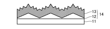
- FIG. 1 is a schematic cross-sectional view showing the configuration of a substrate with a transparent conductive film of the present invention.
- substrate with a transparent conductive film of this invention has the base
- the transparent conductive film 14 includes a first transparent oxide thin film 12 and a second transparent oxide thin film 13 in order from the substrate 11 side.
- the second transparent oxide thin film 13 is conductive and has a crystal structure different from that of the first transparent oxide thin film 12. The angle formed between the substrate 11 and the crystal grain surface of the first transparent oxide thin film 12 is different from the angle formed between the substrate 11 and the crystal grain surface of the second transparent oxide thin film 13.
- the crystal structures of the first transparent oxide thin film 12 and the second transparent oxide thin film 13 are different from each other, whereby the angles formed by the respective crystal grain surfaces can be made different. Thereby, both the long wavelength side light and the short wavelength side light can be reflected in the wavelength region absorbed by the photoelectric conversion layer of the solar cell. For this reason, the photoelectric conversion element using the substrate with a transparent conductive film of the present invention has a concavo-convex shape having a high light confinement effect, and becomes a substrate with a transparent conductive oxide thin film having low resistance and high transmittance.
- the angle formed between the base 11 and the crystal grain surface of the first transparent oxide thin film 12 is preferably larger than the angle formed between the base 11 and the crystal grain surface of the second transparent oxide thin film 13.
- the long wavelength light is scattered by the first transparent oxide thin film 12
- the short wavelength light can be scattered by the second transparent oxide thin film 13 having a large angle.
- it becomes a base
- the substrate with a transparent conductive film of the present invention having the above characteristics can produce a photoelectric conversion element having high photoelectric conversion efficiency when used for a thin film type photoelectric conversion element.
- a conventionally known substrate can be used, and for example, glass, plastic, metal and the like can be used.
- soda lime glass containing an alkali metal such as sodium is used as the substrate 11, in order to prevent an alkali component from diffusing from the substrate 11 to the transparent conductive film 14, the substrate 11 is interposed between the substrate 11 and the transparent conductive film 14.
- an alkali barrier layer As a material constituting such an alkali barrier layer, silicon oxide, aluminum oxide, zirconium oxide, magnesium oxide, or the like can be used.
- a refractive index adjusting layer for reducing the difference in refractive index between the substrate 11 and the alkali barrier layer or the first transparent oxide thin film may be provided.
- the refractive index adjustment layer preferably has a thickness of 20 nm or more and 100 nm or less from the viewpoint of controlling reflection or absorption of transmitted light.
- Such an alkali barrier layer and a refractive index adjusting layer can be formed by a conventionally known film formation method, for example, using an atmospheric pressure CVD method, a spray pyrolysis method, a mist CVD method, a sol-gel method, or the like. can do.
- the transparent conductive film 14 is formed by laminating a first transparent oxide thin film 12 and a second transparent oxide thin film 13.
- the transparent conductive film 14 used in the present invention has a two-layer structure and is characterized in that the size of the crystal grains constituting each is different.
- the average thickness of the transparent conductive film 14 is preferably 200 nm or more and 1500 nm or less. Thereby, light scattering and transparency can be made highly compatible. When the average film thickness of the transparent conductive film 14 is less than 200 nm, sufficient light scattering properties cannot be obtained. If it exceeds 1500 nm, the light transmittance may be lowered. Below, each layer which comprises the transparent conductive film 14 is demonstrated.
- the first transparent oxide thin film 12 is formed on the substrate 11 and is made of a crystalline oxide.
- a first transparent oxide thin film 12 preferably has a layer thickness of 50 nm or more and 1000 nm or less. If it is less than 50 nm, light cannot be sufficiently scattered, and if it exceeds 1000 nm, the translucency of the first transparent oxide thin film 12 is lowered, which is not preferable.
- the first transparent oxide thin film 12 is preferably made of a crystal having a large crystal grain size, more preferably a crystal having a crystal grain size of 200 nm or more and 5000 nm or less.
- the first transparent oxide thin film made of crystals having such a crystal grain size can easily scatter long-wavelength light.
- a 1st transparent oxide thin film is formed with the material of the crystal structure which can form a large crystal grain with a thin film thickness.
- a first transparent oxide thin film that is a thin film and includes large crystal grains can be formed.
- a combination of these scatterings can provide a transparent conductive film that can scatter light in a wide wavelength range.
- the first transparent oxide thin film 12 can be used without any particular limitation as long as it has a crystal structure different from that of the second transparent oxide thin film 13.
- zinc oxide, indium oxide, oxide Magnesium, titanium oxide, or the like can be used.
- the 1st transparent oxide thin film 12 consists of zinc oxide, and it is preferable to have electroconductivity. Thereby, the current generated in the photoelectric conversion layer can be taken out to the outside without loss.
- any production method can be used without any particular limitation.
- atmospheric pressure CVD method spray pyrolysis method, mist CVD method, sputtering method can be used. And so on.
- the second transparent oxide thin film 13 is formed on the first transparent oxide thin film 12, has conductivity, and is made of a crystalline oxide. is there.
- the second transparent oxide thin film 13 can be used without particular limitation as long as it has a crystal structure different from that of the second transparent oxide thin film 13, but the first transparent oxide thin film 13 can be used. From the viewpoint of scattering light having a wavelength different from that of the thin film 12, it is preferable to use a material different from the material constituting the first transparent oxide thin film 12.
- the material constituting the second transparent oxide thin film 13 include tin oxide, zinc oxide, indium oxide, and titanium oxide. Especially, it is preferable that the 2nd transparent oxide thin film 13 consists of tin oxides.
- Such a second transparent oxide thin film 13 is preferably added with a dopant in order to develop conductivity.
- the dopant differs depending on the material constituting the second transparent oxide thin film 13.
- fluorine or antimony is preferably used as a dopant for tin oxide
- boron, aluminum, gallium, indium or the like is preferably used as a dopant for zinc oxide
- indium oxide, Tin or the like is preferably used as a dopant
- niobium or the like is preferably used as a dopant for titanium oxide.
- the second transparent oxide thin film 13 is preferably one having crystal grains smaller than the crystal grains constituting the first transparent oxide thin film 12, and more preferably a crystal grain size of 10 nm to 500 nm. It consists of the crystals of As a result, light having a wavelength narrower than the wavelength of light scattered by the first transparent oxide thin film 12 can be scattered, so that the wavelength region of light scattered by the transparent conductive film can be expanded.
- the same method as the method of manufacturing the first transparent oxide thin film 12 can be used.
- atmospheric pressure CVD method spray pyrolysis method A mist CVD method, a sputtering method, or the like can be used.
- a method for forming a transparent conductive film using a spray pyrolysis method will be described with reference to FIG.
- FIG. 2 is a schematic sectional view showing a spray pyrolysis apparatus for producing a substrate with a transparent conductive film of the present invention.
- a spray pyrolysis apparatus for producing a substrate with a transparent conductive film of the present invention as shown in FIG. 2, a film forming solution 21 containing a film forming material, a piping part for flowing the film forming solution, It comprises a spray unit 22 for injecting a film forming solution flowing through the piping unit onto the substrate 23 and a substrate heating unit 24 for heating the substrate 23.
- Such a spray pyrolysis apparatus forms a transparent conductive film on the entire surface of the substrate 23 by scanning the substrate 23 or scanning the spray unit 22.
- the spray pyrolysis apparatus is not limited to the form shown in FIG. 2, and spraying may be performed using, for example, a structure in which a large number of spray units are arranged on the upper surface of the substrate 23. In this case, it is not always necessary to scan the substrate and the spray unit.
- Example 1 In the present embodiment, an alkali barrier layer, a first transparent oxide thin film 12, and a second transparent oxide thin film 13 are formed in this order on the substrate 11 using the spray pyrolysis apparatus shown in FIG. By forming the film, the transparent conductive film 14 was formed.
- the substrate 23 made of soda lime glass was heated to 450 ° C. by a hot plate (substrate heating unit 24). Then, an alkaline solution in which aluminum acetylacetonate was dissolved in a mixed solution of methanol and water was sprayed onto the substrate 23 with compressed air. In this way, an alkali barrier layer made of aluminum oxide was formed on the substrate.
- the film forming solution was sprayed onto the alkali barrier layer with compressed air for 60 seconds.
- a solution obtained by dissolving zinc acetate in a mixed solution of water and acetic acid was used. In this manner, a first transparent oxide thin film made of zinc oxide was formed on the alkali barrier layer.
- the film forming solution was sprayed onto the first transparent oxide thin film with compressed air for 40 seconds.
- a solution obtained by dissolving stannic chloride and ammonium fluoride in a mixed solution of water, hydrochloric acid and methanol was used.
- a second transparent oxide thin film made of fluorine-doped tin oxide was formed on the first transparent oxide thin film.
- a substrate with a transparent conductive film of this example was produced.
- Example 1 in order to compare the surface shape of the first transparent oxide thin film with the surface shape of the second transparent oxide thin film, the first transparent oxide thin film was formed in the same manner as described above. After forming the film, a sample in which the second transparent oxide thin film was not formed was prepared. Then, the surface of the sample and the surface of the transparent conductive film were observed with an atomic force microscope (AFM).
- AFM atomic force microscope
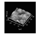
- FIG. 3 is an observation image when the surface of the second transparent oxide thin film is observed by AFM
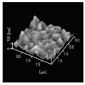
- FIG. 4 is an observation image when the surface of the first transparent oxide thin film is observed by AFM. is there.
- the second transparent oxide thin film has a period of crystal grains of the surface irregularities of the first transparent oxide thin film, while maintaining the period of the crystal grains. It was confirmed that the crystal grains of the second small transparent oxide were laminated. Therefore, it was confirmed that the transparent conductive film produced in Example 1 had a cross section as shown in the cross sectional view of FIG.
- Example 2 A substrate with a transparent conductive film of this example was produced in the same manner as in Example 1 except that the spray spraying time when forming the first transparent oxide thin film was different from Example 1. did. That is, in this example, the spraying time was changed to 40 seconds, and the first transparent oxide thin film was formed on the alkali barrier layer.
- Comparative Example 1 Unlike Example 1, except that the second transparent oxide thin film was formed without forming the first transparent oxide thin film on the alkali barrier layer, it was the same as Example 1. A substrate with a transparent conductive film of Comparative Example 1 was produced.
- FIG. 5 is an image when the surface of the transparent conductive film prepared in Comparative Example 1 is observed with an AFM.
- the angle formed by the substrate of this comparative example and the crystal grain surface of the second transparent oxide thin film is larger than the angle formed by the substrate of Example 1 and the crystal grain surface of the first transparent oxide thin film. It was.
- Comparative Example 2 Compared to Example 1, the second transparent oxide thin film was formed on the alkali barrier layer without forming the first transparent oxide thin film, and the second transparent oxide thin film A substrate with a transparent conductive film of Comparative Example 2 was produced in the same manner as in Example 1 except that the film formation time was changed to 120 seconds.
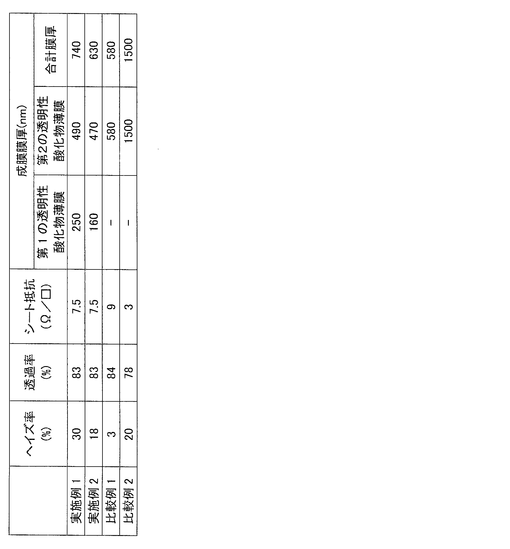
- the haze ratio (%) and the transmittance (%) of light having a wavelength in the visible light region of 400 to 800 nm are measured with respect to the substrate with a transparent conductive film prepared in each Example and each Comparative Example.
- Spectroscopic colorimetry TC-1800H manufactured by Tokyo Denshoku Co., Ltd.
- the haze ratio is a value defined by (diffuse transmittance / total transmittance) ⁇ 100. The results of these measurements are shown in Table 1 below.
- Example 2 (Consideration of Example 2) From the comparison with Examples 1 and 2, by reducing the thickness of the first transparent oxide thin film, the crystal grains of the first transparent oxide thin film are reduced, and the haze ratio of the substrate with the transparent conductive film is increased. It became clear that it could be reduced.
Landscapes
- Chemical & Material Sciences (AREA)
- Engineering & Computer Science (AREA)
- Mechanical Engineering (AREA)
- Metallurgy (AREA)
- General Chemical & Material Sciences (AREA)
- Chemical Kinetics & Catalysis (AREA)
- Physics & Mathematics (AREA)
- Materials Engineering (AREA)
- Inorganic Chemistry (AREA)
- Thermal Sciences (AREA)
- Organic Chemistry (AREA)
- Ceramic Engineering (AREA)
- Non-Insulated Conductors (AREA)
- Photovoltaic Devices (AREA)
- Chemically Coating (AREA)
- Other Surface Treatments For Metallic Materials (AREA)
Description
本発明は、光電変換素子などに用いられる透明導電膜付き基体に関する。
近年、エネルギ問題や、環境問題が盛んに取り上げられている。これらの問題の解決策の一つとして、光電変換素子が注目を集めている。光電変換素子は、太陽光を利用してクリーンなエネルギを供給することができる。光電変換素子の中でも、省資源化に対応し得る薄膜太陽電池が盛んに開発されている。
薄膜太陽電池は、ガラス基板などの基体上に、酸化スズ(SnO2)や酸化亜鉛(ZnO)等の透明導電膜を形成する。そして、透明導電膜上に、光電変換層、透明導電膜、並びに導電膜をこの順に積層する。従来の薄膜太陽電池は、光電変換層としてアモルファスシリコンを用いていたため、短波長側に光電変換感度があった。しかし、近年の薄膜太陽電池は、アモルファスシリコンに加えて、アモルファスシリコンゲルマニウムや微結晶シリコンを積層する。このため、長波長側にも光電変換感度があり、太陽光をより効率的に利用することができる。
薄膜太陽電池の光電変換効率を向上させるための手法として、透明導電膜の表面に凹凸を形成する技術がある。透明導電膜の表面に凹凸を形成することにより、薄膜太陽電池に入射した光を光電変換層内に閉じ込めることができ、光電変換効率を向上させることができる。
また、光電変換効率を向上させるための別の手法として、透明導電膜の透過率を高めることによって、光電変換層に入射する光を取り込みやすくすることも行なわれている。その他にも、透明導電膜の導電性を高めることによって、光電変換層で発生した電流をロスなく外部に取り出すことも行なわれている。
長波長側の光の閉じ込め効果を大きくするためには、透明導電膜の表面に形成する凹凸のピッチを大きくする必要がある。透明導電膜を構成する材料に酸化スズを用いる場合は、透明導電膜の膜厚を厚くすることによって、自然形成される結晶粒径を大きくし、透明導電膜の表面に形成される凹凸を大きくする。
しかしながら、酸化スズからなる透明導電膜は、その抵抗を下げるために多くの自由電子を含ませる必要がある。このため、透明導電膜は、長波長側の光を吸収しやすく、また短波長側の光も僅かに吸収することになり、透過率が減少する。
要するに、酸化スズからなる透明導電膜は、その膜厚を厚くすることによって光閉じ込め効果を向上させることはできるが、光の透過率は減少させることになり、結果として光電変換効率を高めることはできなかった。
この問題を解決するための試みとして、特開平3-125481号公報(特許文献1)には、1.0μmの厚みの第1層と0.2μmの厚みの第2層とを積層した2層構造の透明導電膜が開示されている。特許文献1に開示される透明導電膜は、第1層を結晶粒径の大きな結晶で構成し、第2層を結晶粒径の小さな結晶で構成している。これにより第1層で長波長の光を散乱させるとともに、第2層で短波長の光を散乱する。これにより長波長側の光も短波長側の光も光電変換層に閉じ込める。
また、特開2009-140930号公報(特許文献2)には、基体上に酸化物からなる不連続な小山部を形成し、その上に連続層からなる透明導電膜を形成している。この透明導電膜は、膜厚を厚くすることなく、長波長側の光と短波長側の光とを散乱させることができる。
特許文献1においては、第1層および第2層のいずれも酸化スズで構成されるため、第1層の表面形状は、自然形成されたものと同等となる。そこで、第1層を構成する結晶の粒径を大きくすると、膜厚が厚くなり、透明導電膜の光の吸収量が上昇するため、光電変換効率を低下させることになる。
また、特許文献2に開示される小山部の形成方法では、基体の洗浄状態や材質、濡れ性や成膜時の温度によって小山部の形成が制限されてしまう。このため、小山部の被覆率や粒径、高さなどを制御しにくい。
本発明は、上記のような現状に鑑みてなされたものであり、その目的とするところは、太陽電池の光電変換層にて吸収される波長領域において、高い光閉じ込め効果を有する凹凸形状を備え、かつ低抵抗で高透過率な透明導電膜付き基体を提供することである。
本発明の透明導電膜付き基体は、基体と、該基体上に成膜された透明導電膜とを有し、該透明導電膜は、基体側から順に、第1の透明性酸化物薄膜および第2の透明性酸化物薄膜を有し、第2の透明性酸化物薄膜は、導電性を有し、かつ第1の透明性酸化物薄膜とは結晶構造が異なり、基体と第1の透明性酸化物薄膜の結晶粒表面とのなす角度は、基体と第2の透明性酸化物薄膜の結晶粒表面とのなす角度と異なることを特徴とする。
上記基体と第1の透明性酸化物薄膜の結晶粒表面とのなす角度は、基体と第2の透明性酸化物薄膜の結晶粒表面とのなす角度より大きいことが好ましい。透明導電膜は、その平均膜厚が200nm以上1500nm以下であることが好ましい。第1の透明性酸化物薄膜は、酸化亜鉛であることが好ましく、第2の透明性酸化物薄膜は、酸化スズであることが好ましい。
本発明によれば、太陽電池の光電変換層にて吸収される波長領域において、高い光閉じ込め効果を有する凹凸形状を備え、かつ低抵抗で高透過率な透明導電膜付き基体を提供することができる。
以下、本発明の透明導電膜付き基体について図面を用いて説明する。なお、本発明の図面において、同一の参照符号は、同一部分または相当部分を表わすものである。また、長さ、幅、厚さ、深さなどの寸法関係は図面の明瞭化と簡略化のために適宜に変更されており、実際の寸法関係を表わすものではない。
<透明導電膜付き基体>
図1は、本発明の透明導電膜付き基体の構成を示す模式的な断面図である。本発明の透明導電膜付き基体は、図1に示されるように、基体11と、該基体11上に成膜された透明導電膜14とを有する。透明導電膜14は、基体11側から順に、第1の透明性酸化物薄膜12および第2の透明性酸化物薄膜13を有する。第2の透明性酸化物薄膜13は、導電性を有し、かつ第1の透明性酸化物薄膜12とは結晶構造が異なる。基体11と第1の透明性酸化物薄膜12の結晶粒表面とのなす角度は、基体11と第2の透明性酸化物薄膜13の結晶粒表面とのなす角度と異なる。
図1は、本発明の透明導電膜付き基体の構成を示す模式的な断面図である。本発明の透明導電膜付き基体は、図1に示されるように、基体11と、該基体11上に成膜された透明導電膜14とを有する。透明導電膜14は、基体11側から順に、第1の透明性酸化物薄膜12および第2の透明性酸化物薄膜13を有する。第2の透明性酸化物薄膜13は、導電性を有し、かつ第1の透明性酸化物薄膜12とは結晶構造が異なる。基体11と第1の透明性酸化物薄膜12の結晶粒表面とのなす角度は、基体11と第2の透明性酸化物薄膜13の結晶粒表面とのなす角度と異なる。
このように第1の透明性酸化物薄膜12と第2の透明性酸化物薄膜13との結晶構造が異なることによって、それぞれの結晶粒表面のなす角度を異ならしめることができる。これにより太陽電池の光電変換層に吸収される波長領域において、長波長側の光と短波長側の光との双方を反射することができる。このため、本発明の透明導電膜付き基体を用いた光電変換素子は、高い光閉じ込め効果を有する凹凸形状を備え、かつ低抵抗で高透過率な透明導電性酸化物薄膜付き基体となる。
上記の基体11と第1の透明性酸化物薄膜12の結晶粒表面とのなす角度は、基体11と第2の透明性酸化物薄膜13の結晶粒表面とのなす角度より大きいことが好ましい。これにより第1の透明性酸化物薄膜12で長波長の光を散乱しつつ、角度の大きい第2の透明性酸化物薄膜13で短波長の光を散乱することができる。これにより太陽電池の光電変換層にて吸収される波長領域において、高い光閉じ込め効果を有する凹凸形状を備えた透明導電膜付き基体となる。
上記のような特徴を有する本発明の透明導電膜付き基体は、薄膜型の光電変換素子に用いたときに、高い光電変換効率を有する光電変換素子を作製することができる。
<基体>
本発明の透明導電膜付き基体に用いられる基体11としては、従来公知のものを用いることができ、たとえばガラス、プラスチック、金属などを用いることができる。基体11として、ナトリウムなどのアルカリ金属を含むソーダライムガラスを用いる場合は、基体11から透明導電膜14にアルカリ成分が拡散することを防止するために、基体11と透明導電膜14との間にアルカリバリア層を設けることが好ましい。このようなアルカリバリア層を構成する材料としては、酸化ケイ素、酸化アルミニウム、酸化ジルコニウム、酸化マグネシウムなどを用いることができる。
本発明の透明導電膜付き基体に用いられる基体11としては、従来公知のものを用いることができ、たとえばガラス、プラスチック、金属などを用いることができる。基体11として、ナトリウムなどのアルカリ金属を含むソーダライムガラスを用いる場合は、基体11から透明導電膜14にアルカリ成分が拡散することを防止するために、基体11と透明導電膜14との間にアルカリバリア層を設けることが好ましい。このようなアルカリバリア層を構成する材料としては、酸化ケイ素、酸化アルミニウム、酸化ジルコニウム、酸化マグネシウムなどを用いることができる。
さらに、基体11とアルカリバリア層もしくは第1の透明性酸化物薄膜との屈折率の差を軽減するための屈折率調整層を設けてもよい。屈折率調整層は、透過光の反射または吸収を制御するという観点から、20nm以上100nm以下の厚みであることが好ましい。
このようなアルカリバリア層および屈折率調整層は、従来公知の成膜方法によって成膜することができ、たとえば常圧CVD法、スプレー熱分解法、ミストCVD法、ゾルゲル法などを用いて成膜することができる。
<透明導電膜>
本発明において、透明導電膜14は、第1の透明性酸化物薄膜12と第2の透明性酸化物薄膜13とを積層させたものである。本発明に用いられる透明導電膜14は、2層構造であって、かつそれぞれを構成する結晶粒の大きさが異なることを特徴とする。
本発明において、透明導電膜14は、第1の透明性酸化物薄膜12と第2の透明性酸化物薄膜13とを積層させたものである。本発明に用いられる透明導電膜14は、2層構造であって、かつそれぞれを構成する結晶粒の大きさが異なることを特徴とする。
上記の透明導電膜14は、その平均膜厚が200nm以上1500nm以下であることが好ましい。これにより光の散乱性と透過性とを高度に両立させることができる。透明導電膜14の平均膜厚が200nm未満であると、光の散乱性を十分に得ることができない。1500nmを超えると、光の透過性が低下することがある。以下において、透明導電膜14を構成する各層を説明する。
<第1の透明性酸化物薄膜>
本発明において、第1の透明性酸化物薄膜12は、基体11上に形成されるものであって、結晶性の酸化物からなるものである。このような第1の透明性酸化物薄膜12は、50nm以上1000nm以下の層厚を有することが好ましい。50nm未満であると、光を十分に散乱することができず、1000nmを超えると、第1の透明性酸化物薄膜12の透光性が低下するため好ましくない。
本発明において、第1の透明性酸化物薄膜12は、基体11上に形成されるものであって、結晶性の酸化物からなるものである。このような第1の透明性酸化物薄膜12は、50nm以上1000nm以下の層厚を有することが好ましい。50nm未満であると、光を十分に散乱することができず、1000nmを超えると、第1の透明性酸化物薄膜12の透光性が低下するため好ましくない。
上記の第1の透明性酸化物薄膜12は、結晶粒径の大きな結晶からなることが好ましく、より好ましくは、200nm以上5000nm以下の結晶粒径の結晶からなることである。このような結晶粒径の結晶からなる第1の透明性酸化物薄膜は、長波長の光を散乱しやすくすることができる。
一般に、同一の結晶材料を用いて、大きな結晶粒と小さな結晶粒とを合わせた薄膜を得ようとすると、大きな結晶粒を形成するときに、薄膜の厚みが厚くなりやすい。このため、本発明では、薄い膜厚で大きな結晶粒を形成することができる結晶構造の材料で第1の透明性酸化物薄膜を形成する。これにより薄膜であって、かつ大きな結晶粒からなる第1の透明性酸化物薄膜を形成することができる。
つまり、第1の透明性酸化物薄膜を構成する大きな結晶粒によって長波長の光を散乱させる。そして、第2の透明性酸化物薄膜を構成する小さな結晶粒によって短波長の光を散乱させる。これらの散乱の組合せにより、広範囲の波長領域の光を散乱させることができる透明導電膜を得ることができる。
上記第1の透明性酸化物薄膜12は、第2の透明性酸化物薄膜13と結晶構造が異なるものであれば、特に限定されることなく用いることができ、たとえば酸化亜鉛、酸化インジウム、酸化マグネシウム、または酸化チタンなどを用いることができる。中でも、第1の透明性酸化物薄膜12は、酸化亜鉛からなることが好ましく、導電性を有することが好ましい。これにより光電変換層で発生した電流をロスなく外部に取り出すことができる。
上記の第1の透明性酸化物薄膜12を製造する方法としては、特に限定することなくいかなる製造方法をも用いることができ、たとえば常圧CVD法、スプレー熱分解法、ミストCVD法、スパッタリング法などを挙げることができる。
<第2の透明性酸化物薄膜>
本発明において、第2の透明性酸化物薄膜13は、第1の透明性酸化物薄膜12上に形成されるものであって、かつ導電性を有し、結晶性の酸化物からなるものである。かかる第2の透明性酸化物薄膜13は、第2の透明性酸化物薄膜13と結晶構造が異なるものであれば、特に限定されることなく用いることができるが、第1の透明性酸化物薄膜12とは異なる波長の光を散乱させるという観点から、第1の透明性酸化物薄膜12を構成する材料とは異なるものを用いることが好ましい。第2の透明性酸化物薄膜13を構成する材料としては、たとえば、酸化スズ、酸化亜鉛、酸化インジウム、酸化チタンなどを挙げることができる。中でも、第2の透明性酸化物薄膜13は、酸化スズからなることが好ましい。
本発明において、第2の透明性酸化物薄膜13は、第1の透明性酸化物薄膜12上に形成されるものであって、かつ導電性を有し、結晶性の酸化物からなるものである。かかる第2の透明性酸化物薄膜13は、第2の透明性酸化物薄膜13と結晶構造が異なるものであれば、特に限定されることなく用いることができるが、第1の透明性酸化物薄膜12とは異なる波長の光を散乱させるという観点から、第1の透明性酸化物薄膜12を構成する材料とは異なるものを用いることが好ましい。第2の透明性酸化物薄膜13を構成する材料としては、たとえば、酸化スズ、酸化亜鉛、酸化インジウム、酸化チタンなどを挙げることができる。中でも、第2の透明性酸化物薄膜13は、酸化スズからなることが好ましい。
このような第2の透明性酸化物薄膜13は、導電性を発現させるために、ドーパントを添加することが好ましい。ドーパントとしては、第2の透明性酸化物薄膜13を構成する材料によって異なる。たとえば酸化スズに対しては、フッ素やアンチモン等をドーパントとして用いることが好ましく、酸化亜鉛に対しては、ホウ素、アルミニウム、ガリウム、インジウム等をドーパントとして用いることが好ましく、酸化インジウムに対しては、スズ等をドーパントとして用いることが好ましく、酸化チタンに対してはニオブ等をドーパントとして用いることが好ましい。
第2の透明性酸化物薄膜13は、第1の透明性酸化物薄膜12を構成する結晶粒よりも結晶粒が小さいものを用いることが好ましく、より好ましくは、10nm以上500nm以下の結晶粒径の結晶からなることである。これにより第1の透明性酸化物薄膜12で散乱させる光の波長よりも狭い波長の光を散乱させることができ、もって透明導電膜の散乱させる光の波長領域を広げることができる。
第2の透明性酸化物薄膜13を製造する方法としては、上記の第1の透明性酸化物薄膜12の製造方法と同様のものを用いることができ、たとえば常圧CVD法、スプレー熱分解法、ミストCVD法、スパッタリング法等を用いることができる。以下においては、スプレー熱分解法を用いて透明導電膜を成膜する方法を図2を参照して説明する。
図2は、本発明の透明導電膜付き基体を製造するためのスプレー熱分解装置を示す模式的な断面図である。本発明の透明導電膜付き基体を製造するためのスプレー熱分解装置は、図2に示されるように、成膜材料を含む成膜溶液21と、該成膜溶液を流すための配管部と、該配管部を通って流れた成膜溶液を基体23に噴射するためのスプレー部22と、該基体23を加熱するための基体加熱部24とからなるものである。
このようなスプレー熱分解装置は、基体23を走査させるか、またはスプレー部22を走査させることによって、基体23上の全面に透明導電膜を成膜する。なお、スプレー熱分解装置は、図2に示される形態に限られず、たとえば基体23の上面に多数のスプレー部を配列させたものを用いてスプレーしてもよい。この場合は、必ずしも基体およびスプレー部を走査しなくてもよい。
以下、実施例を挙げて本発明をより詳細に説明するが、本発明はこれらに限定されるものではない。
(実施例1)
本実施例では、図2に示されるスプレー熱分解装置を用いて、基体11上にアルカリバリア層、第1の透明性酸化物薄膜12、および第2の透明性酸化物薄膜13をこの順に成膜することによって透明導電膜14を成膜した。
本実施例では、図2に示されるスプレー熱分解装置を用いて、基体11上にアルカリバリア層、第1の透明性酸化物薄膜12、および第2の透明性酸化物薄膜13をこの順に成膜することによって透明導電膜14を成膜した。
まず、ソーダライムガラスからなる基体23をホットプレート(基体加熱部24)によって450℃まで昇温した。そして、基体23に対し、アルミニウムアセチルアセトナートをメタノールと水との混合液に溶解させたアルカリ溶液を圧縮空気でスプレー噴射した。このようにして、基体上に酸化アルミニウムからなるアルカリバリア層を成膜した。
次に、基体23の温度を450℃に保持したまま、上記のアルカリバリア層上に成膜溶液を60秒間圧縮空気でスプレー噴射した。かかる成膜溶液としては、酢酸亜鉛を水と酢酸との混合液に溶解させたものを用いた。このようにして、アルカリバリア層上に酸化亜鉛からなる第1の透明性酸化物薄膜を成膜した。
次に、基体を500℃に昇温してから、上記の第1の透明性酸化物薄膜上に成膜溶液を40秒間圧縮空気でスプレー噴射した。成膜溶液としては、第2塩化スズおよびフッ化アンモニウムを、水と塩酸とメタノールとの混合溶液に溶解させたものを用いた。このようにして、第1の透明性酸化物薄膜上に、フッ素ドープした酸化スズからなる第2の透明性酸化物薄膜を成膜した。以上のようにして、本実施例の透明導電膜付き基体を作製した。
実施例1において、第1の透明性酸化物薄膜の表面形状と、第2の透明性酸化物薄膜の表面形状とを対比するために、上記と同様の方法で第1の透明性酸化物薄膜を成膜した後に、第2の透明性酸化物薄膜を成膜しないサンプルを作製した。そして、かかるサンプルの表面、および透明導電膜の表面を原子間力顕微鏡(AFM:Atomic Force Microscope)によって観察した。
図3は、第2の透明性酸化物薄膜の表面をAFMで観察したときの観察画像であり、図4は、第1の透明性酸化物薄膜の表面をAFMで観察したときの観察画像である。図3および図4に示される表面形状の観察画像を対比すると、第2の透明性酸化物薄膜は、第1の透明性酸化物薄膜の表面凹凸の結晶粒の周期を保ったまま、その上に小さな第2の透明性酸化物の結晶粒が積層された形状となっていることが確認できた。したがって、実施例1で作製された透明導電膜は、その断面が図1の断面図のようになっていることを確認した。
(実施例2)
実施例1に対し、第1の透明性酸化物薄膜を成膜するときのスプレー噴射時間を変えたことが異なる他は実施例1と同様にして、本実施例の透明導電膜付き基体を作製した。すなわち、本実施例においては、スプレー噴射時間を40秒に変えて、アルカリバリア層上に第1の透明性酸化物薄膜を成膜した。
実施例1に対し、第1の透明性酸化物薄膜を成膜するときのスプレー噴射時間を変えたことが異なる他は実施例1と同様にして、本実施例の透明導電膜付き基体を作製した。すなわち、本実施例においては、スプレー噴射時間を40秒に変えて、アルカリバリア層上に第1の透明性酸化物薄膜を成膜した。
(比較例1)
実施例1に対し、アルカリバリア層上に第1の透明性酸化物薄膜を成膜することなく、第2の透明性酸化物薄膜を成膜したことが異なる他は実施例1と同様にして、比較例1の透明導電膜付き基体を作製した。
実施例1に対し、アルカリバリア層上に第1の透明性酸化物薄膜を成膜することなく、第2の透明性酸化物薄膜を成膜したことが異なる他は実施例1と同様にして、比較例1の透明導電膜付き基体を作製した。
このようにして作製した比較例1の透明導電膜付き基体の表面をAFMで観察した。その結果を図5に示す。図5は、比較例1で作製した透明導電膜の表面をAFMで観察したときの画像である。本比較例の基体と第2の透明性酸化物薄膜の結晶粒表面とのなす角度は、実施例1の基体と第1の透明性酸化物薄膜の結晶粒表面とのなす角度よりも大きくなっていた。
(比較例2)
実施例1に対し、アルカリバリア層上に第1の透明性酸化物薄膜を成膜することなく、第2の透明性酸化物薄膜を成膜したこと、および第2の透明性酸化物薄膜の成膜時間を120秒にしたことが異なる他は、実施例1と同様にして比較例2の透明導電膜付き基体を作製した。
実施例1に対し、アルカリバリア層上に第1の透明性酸化物薄膜を成膜することなく、第2の透明性酸化物薄膜を成膜したこと、および第2の透明性酸化物薄膜の成膜時間を120秒にしたことが異なる他は、実施例1と同様にして比較例2の透明導電膜付き基体を作製した。
<評価結果>
上記の実施例1~2および比較例1~2の透明導電膜付き基体において、第1の透明性酸化物薄膜および第2の透明性酸化物薄膜の膜厚を触針式表面形状測定器(製品名:DEKTAK(株式会社アルバック製))によって測定した。また、透明導電膜のシート抵抗(Ω/□)を4探針抵抗測定器(製品名:ロレスタGP(三菱化学アナリテック株式会社製))によって測定した。さらに、各実施例および各比較例で作製した透明導電膜付き基体に対し、400~800nmの可視光領域の波長の光のヘイズ率(%)および透過率(%)をヘイズメーター(製品名:分光式測色TC-1800H(有限会社東京電色製))によって測定した。なお、ヘイズ率は、(拡散透過率/全透過率)×100で定義される値である。これらの測定の結果を以下の表1に示す。
上記の実施例1~2および比較例1~2の透明導電膜付き基体において、第1の透明性酸化物薄膜および第2の透明性酸化物薄膜の膜厚を触針式表面形状測定器(製品名:DEKTAK(株式会社アルバック製))によって測定した。また、透明導電膜のシート抵抗(Ω/□)を4探針抵抗測定器(製品名:ロレスタGP(三菱化学アナリテック株式会社製))によって測定した。さらに、各実施例および各比較例で作製した透明導電膜付き基体に対し、400~800nmの可視光領域の波長の光のヘイズ率(%)および透過率(%)をヘイズメーター(製品名:分光式測色TC-1800H(有限会社東京電色製))によって測定した。なお、ヘイズ率は、(拡散透過率/全透過率)×100で定義される値である。これらの測定の結果を以下の表1に示す。
(実施例1および2の考察)
実施例1および2に示される結果から、結晶構造の異なる透明導電膜を2層積層することにより、低抵抗であって、かつ高透過率を有するとともに、光電変換層に吸収される波長領域における光散乱性が高い透明導電膜が付いた基体を作製し得ることが明らかとなった。
実施例1および2に示される結果から、結晶構造の異なる透明導電膜を2層積層することにより、低抵抗であって、かつ高透過率を有するとともに、光電変換層に吸収される波長領域における光散乱性が高い透明導電膜が付いた基体を作製し得ることが明らかとなった。
(実施例2の考察)
実施例1および2との対比から、第1の透明性酸化物薄膜の厚みを薄くすることにより、第1の透明性酸化物薄膜の結晶粒を小さくし、透明導電膜付き基体のヘイズ率を低下し得ることが明らかとなった。
実施例1および2との対比から、第1の透明性酸化物薄膜の厚みを薄くすることにより、第1の透明性酸化物薄膜の結晶粒を小さくし、透明導電膜付き基体のヘイズ率を低下し得ることが明らかとなった。
(比較例1の考察)
比較例1のように、第1の透明性酸化物薄膜を成膜しない場合、太陽光の長波長側の光を十分に反射することができなくなるため、ヘイズ率を十分に得ることができなかった。
比較例1のように、第1の透明性酸化物薄膜を成膜しない場合、太陽光の長波長側の光を十分に反射することができなくなるため、ヘイズ率を十分に得ることができなかった。
(比較例2の考察)
比較例2のように、第2の透明性酸化物薄膜の成膜時間を120秒にすることにより、第2の透明性酸化物薄膜の膜厚が厚くなり、その表面に形成される凹凸を大きくすることができたが、その一方で、膜厚が厚くなったことに起因して透過率が低下した。
比較例2のように、第2の透明性酸化物薄膜の成膜時間を120秒にすることにより、第2の透明性酸化物薄膜の膜厚が厚くなり、その表面に形成される凹凸を大きくすることができたが、その一方で、膜厚が厚くなったことに起因して透過率が低下した。
以上のように本発明の実施の形態および実施例について説明を行なったが、上述の各実施の形態および実施例の構成を適宜組み合わせることも当初から予定している。
今回開示された実施の形態および実施例はすべての点で例示であって制限的なものではないと考えられるべきである。本発明の範囲は上記した説明ではなくて請求の範囲によって示され、請求の範囲と均等の意味および範囲内でのすべての変更が含まれることが意図される。
11,23 基体、12 第1の透明性酸化物薄膜、13 第2の透明性酸化物薄膜、14 透明導電膜、21 成膜溶液、22 スプレー部、24 基体加熱部。
Claims (5)
- 基体(11)と、
前記基体(11)上に成膜された透明導電膜(14)とを有し、
前記透明導電膜(14)は、前記基体(11)側から順に、第1の透明性酸化物薄膜(12)および第2の透明性酸化物薄膜(13)を有し、
前記第2の透明性酸化物薄膜(13)は、前記第1の透明性酸化物薄膜(12)とは結晶構造が異なり、
前記基体(11)と前記第1の透明性酸化物薄膜(12)の結晶粒表面とのなす角度は、前記基体(11)と前記第2の透明性酸化物薄膜(13)の結晶粒表面とのなす角度と異なる、透明導電膜付き基体。 - 前記基体(11)と前記第1の透明性酸化物薄膜(12)の結晶粒表面とのなす角度は、前記基体(11)と前記第2の透明性酸化物薄膜(13)の結晶粒表面とのなす角度より大きい、請求項1に記載の透明導電膜付き基体。
- 前記透明導電膜(14)は、その平均膜厚が200nm以上1500nm以下である、請求項1に記載の透明導電膜付き基体。
- 前記第1の透明性酸化物薄膜(12)は、酸化亜鉛からなる、請求項1に記載の透明導電膜付き基体。
- 前記第2の透明性酸化物薄膜(13)は、酸化スズからなる、請求項1に記載の透明導電膜付き基体。
Applications Claiming Priority (2)
| Application Number | Priority Date | Filing Date | Title |
|---|---|---|---|
| JP2010-283321 | 2010-12-20 | ||
| JP2010283321A JP2012132048A (ja) | 2010-12-20 | 2010-12-20 | 透明導電膜付き基体 |
Publications (1)
| Publication Number | Publication Date |
|---|---|
| WO2012086264A2 true WO2012086264A2 (ja) | 2012-06-28 |
Family
ID=46314555
Family Applications (1)
| Application Number | Title | Priority Date | Filing Date |
|---|---|---|---|
| PCT/JP2011/069547 Ceased WO2012086264A2 (ja) | 2010-12-20 | 2011-08-30 | 透明導電膜付き基体 |
Country Status (2)
| Country | Link |
|---|---|
| JP (1) | JP2012132048A (ja) |
| WO (1) | WO2012086264A2 (ja) |
Family Cites Families (7)
| Publication number | Priority date | Publication date | Assignee | Title |
|---|---|---|---|---|
| JPH03125481A (ja) * | 1989-10-09 | 1991-05-28 | Sanyo Electric Co Ltd | 光起電力装置 |
| JPH1185396A (ja) * | 1997-09-10 | 1999-03-30 | Central Glass Co Ltd | タッチパネルの基板用低反射ガラス |
| JP4540311B2 (ja) * | 2003-06-26 | 2010-09-08 | ジオマテック株式会社 | 透明導電膜及びその製造方法 |
| FR2891269B1 (fr) * | 2005-09-23 | 2007-11-09 | Saint Gobain | Substrat transparent muni d'une electrode |
| JP4935114B2 (ja) * | 2006-03-01 | 2012-05-23 | 旭硝子株式会社 | 太陽電池用透明導電性基板およびその製造方法 |
| JP2008186768A (ja) * | 2007-01-31 | 2008-08-14 | Sanyo Electric Co Ltd | 色素増感型太陽電池及びその製造方法 |
| JP2009093911A (ja) * | 2007-10-09 | 2009-04-30 | Panasonic Corp | 透明電極及び透明電極を備えた表示装置 |
-
2010
- 2010-12-20 JP JP2010283321A patent/JP2012132048A/ja active Pending
-
2011
- 2011-08-30 WO PCT/JP2011/069547 patent/WO2012086264A2/ja not_active Ceased
Also Published As
| Publication number | Publication date |
|---|---|
| JP2012132048A (ja) | 2012-07-12 |
Similar Documents
| Publication | Publication Date | Title |
|---|---|---|
| JP5088435B2 (ja) | 太陽電池用透明導電性基板の製造方法 | |
| JP5012793B2 (ja) | 透明導電性酸化物膜付き基体および光電変換素子 | |
| US8362686B2 (en) | Substrate bearing an electrode, organic light-emitting device incorporating it, and its manufacture | |
| JP5330400B2 (ja) | 改良された抵抗率を有する層で被覆したガラス基板 | |
| JP5381912B2 (ja) | 表面電極付透明導電基板及びその製造方法、並びに薄膜太陽電池及びその製造方法 | |
| CN104969362B (zh) | 带表面电极的透明导电玻璃基板及其制造方法、以及薄膜太阳能电池及其制造方法 | |
| US8710357B2 (en) | Transparent conductive structure | |
| CN102834923A (zh) | 具有提高的雾度的基于纳米结构的透明导体以及包含所述透明导体的装置 | |
| JP2011522433A (ja) | 光起電力セルおよび光起電力セル基板 | |
| WO2009142156A1 (ja) | 薄膜光電変換装置用基板とそれを含む薄膜光電変換装置、並びに薄膜光電変換装置用基板の製造方法 | |
| KR101178496B1 (ko) | 이중구조의 투명전도막 및 그 제조방법 | |
| JP2016532994A (ja) | 発光装置用積層体及びその作製方法 | |
| US20110186120A1 (en) | Textured coating with various feature sizes made by using multiple-agent etchant for thin-film solar cells and/or methods of making the same | |
| US20140124030A1 (en) | Thin film solar cell and method for manufacturing same | |
| US20120125432A1 (en) | Transparent conductive substrate for solar cell, and solar cell | |
| WO2005027229A1 (ja) | 透明導電膜付き基体およびその製造方法 | |
| JP2005347490A (ja) | 透明導電性酸化物膜付き基体およびその製造方法ならびに光電変換素子 | |
| JPWO2012169602A1 (ja) | 透明導電膜付き基板 | |
| WO2012086264A2 (ja) | 透明導電膜付き基体 | |
| JPWO2006046397A1 (ja) | 薄膜光電変換装置用基板およびそれを用いた集積型薄膜光電変換装置 | |
| JP2013006735A (ja) | 透明導電膜付きガラス板およびその製造方法 | |
| US20110020621A1 (en) | Glass-type substrate coated with thin layers and production method | |
| JP2013131318A (ja) | 薄膜の製造方法および製造装置 | |
| TWI429099B (zh) | 具有寬帶光散射功能的基板及其製造方法 | |
| JPWO2010023867A1 (ja) | 薄膜太陽電池及びその製造方法、並びに薄膜太陽電池用基板 |
Legal Events
| Date | Code | Title | Description |
|---|---|---|---|
| 121 | Ep: the epo has been informed by wipo that ep was designated in this application |
Ref document number: 11850201 Country of ref document: EP Kind code of ref document: A2 |
|
| NENP | Non-entry into the national phase |
Ref country code: DE |
|
| 122 | Ep: pct application non-entry in european phase |
Ref document number: 11850201 Country of ref document: EP Kind code of ref document: A2 |