WO2012081584A1 - マイクロチップの製造方法およびマイクロチップ - Google Patents
マイクロチップの製造方法およびマイクロチップ Download PDFInfo
- Publication number
- WO2012081584A1 WO2012081584A1 PCT/JP2011/078815 JP2011078815W WO2012081584A1 WO 2012081584 A1 WO2012081584 A1 WO 2012081584A1 JP 2011078815 W JP2011078815 W JP 2011078815W WO 2012081584 A1 WO2012081584 A1 WO 2012081584A1
- Authority
- WO
- WIPO (PCT)
- Prior art keywords
- substrate
- light
- microchip
- recess
- concave portion
- Prior art date
- Legal status (The legal status is an assumption and is not a legal conclusion. Google has not performed a legal analysis and makes no representation as to the accuracy of the status listed.)
- Ceased
Links
Images




Classifications
-
- B—PERFORMING OPERATIONS; TRANSPORTING
- B01—PHYSICAL OR CHEMICAL PROCESSES OR APPARATUS IN GENERAL
- B01L—CHEMICAL OR PHYSICAL LABORATORY APPARATUS FOR GENERAL USE
- B01L3/00—Containers or dishes for laboratory use, e.g. laboratory glassware; Droppers
- B01L3/50—Containers for the purpose of retaining a material to be analysed, e.g. test tubes
- B01L3/502—Containers for the purpose of retaining a material to be analysed, e.g. test tubes with fluid transport, e.g. in multi-compartment structures
- B01L3/5027—Containers for the purpose of retaining a material to be analysed, e.g. test tubes with fluid transport, e.g. in multi-compartment structures by integrated microfluidic structures, i.e. dimensions of channels and chambers are such that surface tension forces are important, e.g. lab-on-a-chip
- B01L3/502707—Containers for the purpose of retaining a material to be analysed, e.g. test tubes with fluid transport, e.g. in multi-compartment structures by integrated microfluidic structures, i.e. dimensions of channels and chambers are such that surface tension forces are important, e.g. lab-on-a-chip characterised by the manufacture of the container or its components
-
- B—PERFORMING OPERATIONS; TRANSPORTING
- B29—WORKING OF PLASTICS; WORKING OF SUBSTANCES IN A PLASTIC STATE IN GENERAL
- B29C—SHAPING OR JOINING OF PLASTICS; SHAPING OF MATERIAL IN A PLASTIC STATE, NOT OTHERWISE PROVIDED FOR; AFTER-TREATMENT OF THE SHAPED PRODUCTS, e.g. REPAIRING
- B29C65/00—Joining or sealing of preformed parts, e.g. welding of plastics materials; Apparatus therefor
- B29C65/02—Joining or sealing of preformed parts, e.g. welding of plastics materials; Apparatus therefor by heating, with or without pressure
- B29C65/14—Joining or sealing of preformed parts, e.g. welding of plastics materials; Apparatus therefor by heating, with or without pressure using wave energy, i.e. electromagnetic radiation, or particle radiation
- B29C65/16—Laser beams
- B29C65/1629—Laser beams characterised by the way of heating the interface
- B29C65/1635—Laser beams characterised by the way of heating the interface at least passing through one of the parts to be joined, i.e. laser transmission welding
-
- B—PERFORMING OPERATIONS; TRANSPORTING
- B29—WORKING OF PLASTICS; WORKING OF SUBSTANCES IN A PLASTIC STATE IN GENERAL
- B29C—SHAPING OR JOINING OF PLASTICS; SHAPING OF MATERIAL IN A PLASTIC STATE, NOT OTHERWISE PROVIDED FOR; AFTER-TREATMENT OF THE SHAPED PRODUCTS, e.g. REPAIRING
- B29C65/00—Joining or sealing of preformed parts, e.g. welding of plastics materials; Apparatus therefor
- B29C65/02—Joining or sealing of preformed parts, e.g. welding of plastics materials; Apparatus therefor by heating, with or without pressure
- B29C65/14—Joining or sealing of preformed parts, e.g. welding of plastics materials; Apparatus therefor by heating, with or without pressure using wave energy, i.e. electromagnetic radiation, or particle radiation
- B29C65/16—Laser beams
- B29C65/1687—Laser beams making use of light guides
- B29C65/169—Laser beams making use of light guides being a part of the joined article
-
- B—PERFORMING OPERATIONS; TRANSPORTING
- B29—WORKING OF PLASTICS; WORKING OF SUBSTANCES IN A PLASTIC STATE IN GENERAL
- B29C—SHAPING OR JOINING OF PLASTICS; SHAPING OF MATERIAL IN A PLASTIC STATE, NOT OTHERWISE PROVIDED FOR; AFTER-TREATMENT OF THE SHAPED PRODUCTS, e.g. REPAIRING
- B29C66/00—General aspects of processes or apparatus for joining preformed parts
- B29C66/01—General aspects dealing with the joint area or with the area to be joined
- B29C66/05—Particular design of joint configurations
- B29C66/10—Particular design of joint configurations particular design of the joint cross-sections
- B29C66/11—Joint cross-sections comprising a single joint-segment, i.e. one of the parts to be joined comprising a single joint-segment in the joint cross-section
- B29C66/112—Single lapped joints
-
- B—PERFORMING OPERATIONS; TRANSPORTING
- B29—WORKING OF PLASTICS; WORKING OF SUBSTANCES IN A PLASTIC STATE IN GENERAL
- B29C—SHAPING OR JOINING OF PLASTICS; SHAPING OF MATERIAL IN A PLASTIC STATE, NOT OTHERWISE PROVIDED FOR; AFTER-TREATMENT OF THE SHAPED PRODUCTS, e.g. REPAIRING
- B29C66/00—General aspects of processes or apparatus for joining preformed parts
- B29C66/01—General aspects dealing with the joint area or with the area to be joined
- B29C66/05—Particular design of joint configurations
- B29C66/10—Particular design of joint configurations particular design of the joint cross-sections
- B29C66/11—Joint cross-sections comprising a single joint-segment, i.e. one of the parts to be joined comprising a single joint-segment in the joint cross-section
- B29C66/114—Single butt joints
-
- B—PERFORMING OPERATIONS; TRANSPORTING
- B29—WORKING OF PLASTICS; WORKING OF SUBSTANCES IN A PLASTIC STATE IN GENERAL
- B29C—SHAPING OR JOINING OF PLASTICS; SHAPING OF MATERIAL IN A PLASTIC STATE, NOT OTHERWISE PROVIDED FOR; AFTER-TREATMENT OF THE SHAPED PRODUCTS, e.g. REPAIRING
- B29C66/00—General aspects of processes or apparatus for joining preformed parts
- B29C66/50—General aspects of joining tubular articles; General aspects of joining long products, i.e. bars or profiled elements; General aspects of joining single elements to tubular articles, hollow articles or bars; General aspects of joining several hollow-preforms to form hollow or tubular articles
- B29C66/51—Joining tubular articles, profiled elements or bars; Joining single elements to tubular articles, hollow articles or bars; Joining several hollow-preforms to form hollow or tubular articles
- B29C66/53—Joining single elements to tubular articles, hollow articles or bars
- B29C66/534—Joining single elements to open ends of tubular or hollow articles or to the ends of bars
- B29C66/5346—Joining single elements to open ends of tubular or hollow articles or to the ends of bars said single elements being substantially flat
- B29C66/53461—Joining single elements to open ends of tubular or hollow articles or to the ends of bars said single elements being substantially flat joining substantially flat covers and/or substantially flat bottoms to open ends of container bodies
-
- B—PERFORMING OPERATIONS; TRANSPORTING
- B81—MICROSTRUCTURAL TECHNOLOGY
- B81C—PROCESSES OR APPARATUS SPECIALLY ADAPTED FOR THE MANUFACTURE OR TREATMENT OF MICROSTRUCTURAL DEVICES OR SYSTEMS
- B81C3/00—Assembling of devices or systems from individually processed components
- B81C3/001—Bonding of two components
-
- B—PERFORMING OPERATIONS; TRANSPORTING
- B01—PHYSICAL OR CHEMICAL PROCESSES OR APPARATUS IN GENERAL
- B01L—CHEMICAL OR PHYSICAL LABORATORY APPARATUS FOR GENERAL USE
- B01L2300/00—Additional constructional details
- B01L2300/06—Auxiliary integrated devices, integrated components
- B01L2300/0627—Sensor or part of a sensor is integrated
- B01L2300/0654—Lenses; Optical fibres
-
- B—PERFORMING OPERATIONS; TRANSPORTING
- B29—WORKING OF PLASTICS; WORKING OF SUBSTANCES IN A PLASTIC STATE IN GENERAL
- B29C—SHAPING OR JOINING OF PLASTICS; SHAPING OF MATERIAL IN A PLASTIC STATE, NOT OTHERWISE PROVIDED FOR; AFTER-TREATMENT OF THE SHAPED PRODUCTS, e.g. REPAIRING
- B29C65/00—Joining or sealing of preformed parts, e.g. welding of plastics materials; Apparatus therefor
- B29C65/02—Joining or sealing of preformed parts, e.g. welding of plastics materials; Apparatus therefor by heating, with or without pressure
- B29C65/14—Joining or sealing of preformed parts, e.g. welding of plastics materials; Apparatus therefor by heating, with or without pressure using wave energy, i.e. electromagnetic radiation, or particle radiation
- B29C65/16—Laser beams
- B29C65/1603—Laser beams characterised by the type of electromagnetic radiation
- B29C65/1612—Infrared [IR] radiation, e.g. by infrared lasers
- B29C65/1616—Near infrared radiation [NIR], e.g. by YAG lasers
-
- B—PERFORMING OPERATIONS; TRANSPORTING
- B29—WORKING OF PLASTICS; WORKING OF SUBSTANCES IN A PLASTIC STATE IN GENERAL
- B29C—SHAPING OR JOINING OF PLASTICS; SHAPING OF MATERIAL IN A PLASTIC STATE, NOT OTHERWISE PROVIDED FOR; AFTER-TREATMENT OF THE SHAPED PRODUCTS, e.g. REPAIRING
- B29C65/00—Joining or sealing of preformed parts, e.g. welding of plastics materials; Apparatus therefor
- B29C65/02—Joining or sealing of preformed parts, e.g. welding of plastics materials; Apparatus therefor by heating, with or without pressure
- B29C65/14—Joining or sealing of preformed parts, e.g. welding of plastics materials; Apparatus therefor by heating, with or without pressure using wave energy, i.e. electromagnetic radiation, or particle radiation
- B29C65/16—Laser beams
- B29C65/1677—Laser beams making use of an absorber or impact modifier
-
- B—PERFORMING OPERATIONS; TRANSPORTING
- B29—WORKING OF PLASTICS; WORKING OF SUBSTANCES IN A PLASTIC STATE IN GENERAL
- B29C—SHAPING OR JOINING OF PLASTICS; SHAPING OF MATERIAL IN A PLASTIC STATE, NOT OTHERWISE PROVIDED FOR; AFTER-TREATMENT OF THE SHAPED PRODUCTS, e.g. REPAIRING
- B29C66/00—General aspects of processes or apparatus for joining preformed parts
- B29C66/70—General aspects of processes or apparatus for joining preformed parts characterised by the composition, physical properties or the structure of the material of the parts to be joined; Joining with non-plastics material
- B29C66/71—General aspects of processes or apparatus for joining preformed parts characterised by the composition, physical properties or the structure of the material of the parts to be joined; Joining with non-plastics material characterised by the composition of the plastics material of the parts to be joined
-
- B—PERFORMING OPERATIONS; TRANSPORTING
- B29—WORKING OF PLASTICS; WORKING OF SUBSTANCES IN A PLASTIC STATE IN GENERAL
- B29C—SHAPING OR JOINING OF PLASTICS; SHAPING OF MATERIAL IN A PLASTIC STATE, NOT OTHERWISE PROVIDED FOR; AFTER-TREATMENT OF THE SHAPED PRODUCTS, e.g. REPAIRING
- B29C66/00—General aspects of processes or apparatus for joining preformed parts
- B29C66/70—General aspects of processes or apparatus for joining preformed parts characterised by the composition, physical properties or the structure of the material of the parts to be joined; Joining with non-plastics material
- B29C66/73—General aspects of processes or apparatus for joining preformed parts characterised by the composition, physical properties or the structure of the material of the parts to be joined; Joining with non-plastics material characterised by the intensive physical properties of the material of the parts to be joined, by the optical properties of the material of the parts to be joined, by the extensive physical properties of the parts to be joined, by the state of the material of the parts to be joined or by the material of the parts to be joined being a thermoplastic or a thermoset
- B29C66/739—General aspects of processes or apparatus for joining preformed parts characterised by the composition, physical properties or the structure of the material of the parts to be joined; Joining with non-plastics material characterised by the intensive physical properties of the material of the parts to be joined, by the optical properties of the material of the parts to be joined, by the extensive physical properties of the parts to be joined, by the state of the material of the parts to be joined or by the material of the parts to be joined being a thermoplastic or a thermoset characterised by the material of the parts to be joined being a thermoplastic or a thermoset
- B29C66/7392—General aspects of processes or apparatus for joining preformed parts characterised by the composition, physical properties or the structure of the material of the parts to be joined; Joining with non-plastics material characterised by the intensive physical properties of the material of the parts to be joined, by the optical properties of the material of the parts to be joined, by the extensive physical properties of the parts to be joined, by the state of the material of the parts to be joined or by the material of the parts to be joined being a thermoplastic or a thermoset characterised by the material of the parts to be joined being a thermoplastic or a thermoset characterised by the material of at least one of the parts being a thermoplastic
- B29C66/73921—General aspects of processes or apparatus for joining preformed parts characterised by the composition, physical properties or the structure of the material of the parts to be joined; Joining with non-plastics material characterised by the intensive physical properties of the material of the parts to be joined, by the optical properties of the material of the parts to be joined, by the extensive physical properties of the parts to be joined, by the state of the material of the parts to be joined or by the material of the parts to be joined being a thermoplastic or a thermoset characterised by the material of the parts to be joined being a thermoplastic or a thermoset characterised by the material of at least one of the parts being a thermoplastic characterised by the materials of both parts being thermoplastics
-
- B—PERFORMING OPERATIONS; TRANSPORTING
- B29—WORKING OF PLASTICS; WORKING OF SUBSTANCES IN A PLASTIC STATE IN GENERAL
- B29L—INDEXING SCHEME ASSOCIATED WITH SUBCLASS B29C, RELATING TO PARTICULAR ARTICLES
- B29L2031/00—Other particular articles
- B29L2031/756—Microarticles, nanoarticles
Definitions
- the present invention relates to a microchip manufacturing method and a microchip.
- microchips In recent years, the importance of detecting, detecting or quantifying biological substances such as DNA (Deoxyribo Nucleic Acid), enzymes, antigens, antibodies, proteins, viruses and cells, and chemical substances in the fields of medicine, health, food, drug discovery, etc. There have been proposed various biochips and microchemical chips (hereinafter collectively referred to as microchips) that can be easily measured.
- a microchip has a fluid circuit therein, and the fluid circuit processes, for example, a sample (for example, blood) to be examined / analyzed or a liquid for reacting with the sample.
- a liquid reagent holding chamber for holding a reagent; a measuring unit for measuring a sample or a liquid reagent; a mixing chamber for mixing the sample and the liquid reagent; a detecting unit for analyzing and / or examining the mixed solution And the like, and fine channels (width of about several hundred ⁇ m) that appropriately connect these parts.
- a microchip having such a fluid circuit can perform a series of experiments and analysis operations performed in a laboratory within a chip of several centimeters square and several millimeters in thickness. It has many advantages such as low cost, fast reaction speed, high throughput testing, and the ability to obtain test results immediately at the sample collection site. Suitable for biochemical tests such as blood tests. It is used for.
- a microchip is usually manufactured by bonding a substrate on which a recess (groove) constituting a fluid circuit is formed and a flat substrate.
- welding by irradiation of light has been used for bonding two substrates made of thermoplastic resin (for example, Japanese Patent Publication No. 62-49850 (Patent Document 1)).
- one of the two thermoplastic resin substrates is a light-transmitting substrate and the other is a light-absorbing substrate. Irradiate light from the side. When the temperature of the bonded surface exceeds the melting point due to light irradiation, the substrates are melted and the two substrates are bonded.
- the welding by light irradiation as described in Patent Document 1 has the following problems. That is, usually, when a light-transmitting substrate and a light-absorbing substrate are bonded together, the entire surface of the light-transmitting substrate is irradiated with light. At this time, the light-transmitting substrate and the light-absorbing substrate are bonded together. If the amount of light irradiated to the part (contact part) is not sufficient, poor bonding occurs. On the other hand, when the irradiation light quantity is increased, not only the light irradiation for a long time is required and the productivity is lowered, but also damage to other than the bonded portion is increased. For example, in the production of a microchip as described above, if the amount of irradiation light is excessively large, the capacity may change due to deformation of the measuring unit, or a fine flow path connecting each unit may be blocked. .
- a step of disposing a light-absorbing second substrate on a recess-forming surface of a light-transmitting first substrate having a recess on one surface, and irradiating light from the first substrate side Accordingly, a method of manufacturing a microchip comprising the step of welding the first substrate and the second substrate, wherein at least a part of the light irradiated toward the recess is formed between the first substrate and the second substrate.
- substrates, and the microchip obtained by this manufacturing method are provided.
- the first substrate has a surface that forms an angle of more than 0 degrees and less than 90 degrees with respect to the light traveling direction on at least a part of the outer surface of the region facing the recess.
- the side wall forming the concave portion of the first substrate has a tapered shape such that the width of the side wall becomes smaller as it goes to the bonding portion between the first substrate and the second substrate.
- the traveling direction of the light incident on the outer surface of the first substrate is preferably a direction that forms an angle of more than 0 degrees and less than 90 degrees with respect to the outer surface.
- the present invention also provides a light-transmitting first substrate having a recess on one surface, and light absorption welded to the recess-forming surface of the first substrate by irradiation of light from the first substrate side.
- a second substrate, and the first substrate condenses at least a part of the light irradiated toward the concave portion on the bonding portion between the first substrate and the second substrate.
- a microchip having an optical part is provided.
- the condensing portion is a surface of the first substrate that forms at least a part of an outer surface of the region facing the concave portion and has an angle of more than 0 degrees and less than 90 degrees with respect to the light traveling direction. It is preferable to include.
- the condensing portion is a side wall that forms a concave portion of the first substrate, and has a tapered shape such that the width of the side wall decreases as it goes toward the bonding portion between the first substrate and the second substrate. It is preferable to include the side wall which has.
- a microchip manufacturing method in which substrates are bonded to each other by welding by light irradiation, and a microchip having excellent adhesion between substrates while preventing or reducing deformation of a fluid circuit with high productivity.
- a method of manufacturing a microchip that can be manufactured can be provided.
- the manufacturing method of the microchip of the present invention includes the following steps: (A) a substrate stacking step of disposing a light-absorbing second substrate on the concave-forming surface of the light-transmitting first substrate having a concave portion on one surface; and (B) from the first substrate side.
- thermoplastic resin can be used for the first substrate.
- thermoplastic resins include polyethylene terephthalate (PET), polyethylene naphthalate (PEN), polybutylene terephthalate (PBT), polymethyl methacrylate (PMMA), polycarbonate (PC), polystyrene (PS), polypropylene (PP), polyethylene (PE), polyarylate resin (PAR), acrylonitrile butadiene styrene resin (ABS), vinyl chloride resin (PVC), polymethylpentene resin (PMP), polybutadiene resin (PBD), styrene butadiene resin (Styrene-butadiene copolymer), biodegradable polymer (BP), cycloolefin polymer (COP), polydimethylsiloxane (PDMS), polyacetal (POM), polyamide (PA), etc. It can gel.
- PET polyethylene terephthalate
- PEN polyethylene naphthalate
- PBT polybutylene
- a concave portion (groove) having a predetermined pattern for forming a fluid circuit inside the microchip is formed on one surface of the first substrate (the surface on which the second substrate is laminated).
- the method for forming the recess (groove) constituting the fluid circuit on the substrate surface is not particularly limited, and examples thereof include an injection molding method using a mold having a transfer structure, an imprint method, and the like.
- the fluid circuit of the microchip is composed of a hollow portion constituted by a concave portion provided on the surface of the first substrate and a surface of the second substrate facing the first substrate.
- the shape (pattern) of the recess formed on the surface of the first substrate is determined so that the hollow portion has a desired fluid circuit structure.
- the first substrate receives at least part of the light emitted toward the recesses between the first substrate and the second substrate.
- a condensing part for condensing light on the bonding part is provided.
- the second substrate is a light-absorbing substrate, and can be composed of, for example, a thermoplastic resin in which a light-absorbing substance that absorbs light and generates heat is dispersed.
- a thermoplastic resin in which a light-absorbing substance that absorbs light and generates heat is dispersed.
- the thermoplastic resin that can be used for the second substrate are the same as described above.
- the light absorbing substance include a dye, and among these, carbon black can be preferably used.
- the light absorbing material only needs to be dispersed on at least the bonding surface of the second substrate. For example, a structure in which a layer in which a light absorbing material is dispersed is formed on the bonding surface side of the substrate, or the light absorbing material may be dispersed throughout the second substrate.
- the first substrate and the second substrate may be made of different types of thermoplastic resins, but are preferably made of the same kind of thermoplastic resin.
- the bonding surfaces of both the substrates are simultaneously melted by light irradiation, so that the adhesive strength can be further increased.
- the size of the first and second substrates is not particularly limited, and can be, for example, about several centimeters in length and width and about several millimeters to 1 cm in thickness.
- the fluid circuit includes, for example, a reagent holding unit for holding a reagent for mixing or reacting with a sample to be examined or analyzed; a separation unit for taking out a specific component from the sample introduced into the fluid circuit; Specimen measuring unit for measuring a sample (including a specific component in the sample; the same shall apply hereinafter); a reagent measuring unit for measuring a reagent; a mixing unit for mixing the sample and the reagent; And a detection unit for performing inspection or analysis (for example, detection or quantification of a specific component in a mixed solution).
- a reagent holding unit for holding a reagent for mixing or reacting with a sample to be examined or analyzed
- a separation unit for taking out a specific component from the sample introduced into the fluid circuit
- Specimen measuring unit for measuring a sample (including a specific component in the sample; the same shall apply hereinafter)
- a reagent measuring unit for measuring a reagent
- a mixing unit for mixing the sample
- the method of inspection or analysis is not particularly limited, and examples thereof include optical measurement such as a method of detecting the intensity (transmittance) of light transmitted by irradiating light to the detection unit.
- the microchip according to the present invention may have all of the above-described exemplified portions, or may not have any one or more. Moreover, you may have site
- the fluid treatment can be performed by sequentially applying centrifugal force in an appropriate direction to the microchip.
- Application of centrifugal force to the microchip can be performed by placing the microchip on a device (centrifuge) that can apply centrifugal force.
- the centrifuge device can include a rotatable rotor (rotor) and a rotatable stage disposed on the rotor.
- a centrifugal force in an arbitrary direction can be applied to the microchip by placing the microchip on the stage and rotating the stage to arbitrarily set the angle of the microchip with respect to the rotor.
- the second substrate is disposed on the recess forming surface of the first substrate.
- a glass plate or the like is placed on the first substrate, and light (for example, laser light) is applied with pressure applied to the first and second substrates through the glass plate or the like. ) Is irradiated from the first substrate side (glass plate side), and the entire first substrate is scanned to weld the substrates. By applying pressure, welding can be performed in a state where the first substrate and the second substrate are in close contact with each other without a gap.
- the light-absorbing substance generates heat by light irradiation, and this heat causes the bonding surface of the second substrate (first substrate side surface), and in some cases, the bonding surface of the first substrate (second substrate side surface). ) Is melted and the substrates are welded together.
- Irradiation light is not particularly limited as long as a light absorbing material such as carbon black absorbs light and can heat the bonding surface relatively efficiently.
- the wavelength is about 0.8 to 1.1 ⁇ m
- Laser light with a power of about 10 to 1000 W can be used.
- the present invention in the light irradiation in the welding step (B), at least part of the light irradiated toward the concave portion forming the fluid circuit of the microchip is generated between the first substrate and the second substrate. It is performed so that it may be condensed on the bonding part (contact part).
- the amount of light irradiated to reach the bonding portion (contact portion) between the first substrate and the second substrate without increasing the irradiation intensity or irradiation time of the light source is compared with the case where the light is not condensed. Therefore, the adhesion between the substrates can be improved. Moreover, since it is not necessary to increase irradiation time, productivity can be maintained favorable.
- the light irradiated toward the region where light irradiation is unnecessary is the first light. Since it can be turned to the bonding portion between the substrate and the second substrate, it is possible to simultaneously prevent deformation of the fluid circuit and improve adhesion between the substrates.
- FIG. 1 shows an example in which a condensing part is provided on a first substrate of a microchip in order to condense irradiating light on a bonded part of a first substrate and a second substrate. It is a schematic sectional drawing which shows a light effect.
- FIG. 1A and FIG. 1B both show the state of light irradiation from the first substrate 100 side in the welding step (B), and FIG. 1A shows the first substrate 100.
- FIG. 1B shows the light traveling direction when the first substrate 100 has the light converging part 400.
- the condensing unit 400 is an inclined surface (inclined plane) that constitutes a part of the outer surface of the first substrate 100 that faces the concave portion 500, specifically, with respect to the traveling direction of the light 300. It consists of a surface that forms an angle greater than 0 degrees and less than 90 degrees.
- the light 300 irradiated from the direction perpendicular to the substrate surface of the first substrate 100 toward the concave portion 500 is directly used as the first light.
- the substrate 100 and the concave portion 500 go straight and reach the surface of the second substrate 200 facing the concave portion 500.
- Such irradiation light can cause deformation of the surface of the second substrate 200, and thus the fluid circuit.
- FIG. 1B when the light collecting unit 400 is provided on the outer surface of the first substrate 100, the light 300 incident on the inclined surface of the light collecting unit 400 is reflected on the first substrate 100.
- the light is focused on the bonding portion between the first substrate 100 and the second substrate 200 without reaching the surface of the second substrate 200.
- an inclined surface (condenser 400) having a width of 0.75 is formed adjacent to a wall X having a width of 1.0 provided on the outer surface of the first substrate 100.
- the incident angle ⁇ 1 of the light 300 to the light converging unit 400 is 60 °
- the refractive index of the thermoplastic resin constituting the first substrate 100 is 1.5. . Therefore, according to Snell's law, the refraction angle ⁇ 2 is 35 °.
- the condensing part 400 may be provided in the whole area
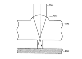
- the light condensing unit according to the present embodiment is not limited to the inclined plane as shown in FIG. 1, but the outer surface (usually normal) of the first substrate 100 as shown in FIGS. 2 and 3. May be a condensing part 405 made of a convex surface (lens surface) provided immediately above the bonding part.
- the focal length f of the convex surface is set to be the same (or substantially the same) as the thickness of the first substrate 100 (the distance from the outer surface to the bonded portion).
- FIG. 4 shows another example in which a condensing part is provided on the first substrate of the microchip in order to condense the irradiation light on the bonding part of the first substrate and the second substrate, and the condensing part. It is a schematic sectional drawing which shows the condensing effect by. 4A and 4B both show the state of light irradiation from the first substrate 100 side in the welding step (B), and FIG. 4A shows the first substrate 100. FIG. 4B shows the light traveling direction when the first substrate 100 has the light condensing part 410.
- FIG. 4A and 4B both show the state of light irradiation from the first substrate 100 side in the welding step (B), and FIG. 4A shows the first substrate 100.
- FIG. 4B shows the light traveling direction when the first substrate 100 has the light condensing part 410.
- the light converging unit 410 is directed to a tapered side wall that forms the concave portion 500 of the first substrate 100, specifically, to a bonding portion between the first substrate 100 and the second substrate 200. Therefore, it consists of an inclined side wall (side wall having an inclined side wall surface) whose width is reduced.
- the inclination angle of the inclined side wall surface of the side wall that is the condensing part 410 (the angle formed between the inclined side wall and the traveling direction of the light 300), that is, the taper angle ⁇ in FIG. 4B is 0 ° ⁇ ⁇ .
- FIG. 4B shows an example in which concave portions 500 are formed on both sides of the side wall, and two opposing side wall surfaces that form these concave portions 500 are inclined, but only one side wall surface is inclined. You may do it.
- the light collecting portion in the case where the light collecting portion is not provided, irradiation is performed from a direction perpendicular to the substrate surface of the first substrate 100 toward the concave portion 500 as in the case of FIG.
- the light 300 thus traveled straight through the first substrate 100 and the recess 500 and reaches the surface of the second substrate 200 facing the recess 500.
- the light condensing unit 410 having a tapered side wall when the light condensing unit 410 having a tapered side wall is provided, the light 300 is reflected by the inclined side wall surface of the light condensing unit 410 (preferably total reflection). Then, the light is condensed on the bonding portion between the first substrate 100 and the second substrate 200 without reaching the surface of the second substrate 200 facing the recess.
- inclined surfaces are formed over both sides of the sidewall Y having a width of 1.0 shown in FIG. And the amount of light applied to the bonding portion between the second substrate 200 and the second substrate 200 are increased by 2.5 times.
- the deformation of the surface of the second substrate 200 located immediately below the inclined sidewall surface of the light condensing unit 410 (the sidewall forming the recess 500) and the first substrate are prevented. Improvement of the adhesiveness of the bonded portion between the second substrate 200 and the second substrate 200 can be achieved at the same time.
- FIG. 5 shows still another example in which a condensing unit is provided on the first substrate of the microchip in order to condense the irradiation light on the bonded portion of the first substrate and the second substrate, and the condensing It is a schematic sectional drawing which shows the condensing effect by a part.
- FIG. 5A is a diagram showing the traveling direction of light when the first substrate 100 does not have a condensing part, and is the same as FIG.
- FIG. 5B shows the traveling direction of light when the first substrate 100 includes the light collecting unit according to the present embodiment.
- the first substrate 100 includes the two light-collecting portions 400 that are the inclined surfaces that constitute a part of the outer surface facing the concave portion 500 described in the first embodiment, and the second substrate 100.
- the two condensing parts 410 which consist of the side wall of the taper shape which forms the recessed part 500 demonstrated in embodiment are included.
- an inclined surface (condensing portion 400) having a width of 0.75 is formed adjacent to both sides of a wall Z having a width of 1.0 provided on the outer surface of the first substrate 100.
- the inclined side wall surface (condenser 410) that reflects (totally reflects) incident light the amount of light applied to the bonded portion of the first substrate 100 and the second substrate 200 Increased 3.6 times.
- the light collecting effect can be further improved.
- FIG. 6 is a schematic cross-sectional view showing an example of irradiating light obliquely in order to condense the irradiating light on the bonding portion between the first substrate and the second substrate.
- 6A and 6B both show the state of light irradiation from the first substrate 100 side in the welding step (B), and FIG. 6A shows the first substrate 100.
- FIG. 6B shows a light traveling direction when light is irradiated from a direction perpendicular to the outer surface (substrate surface) of the first substrate 100, and light is irradiated obliquely with respect to the outer surface (substrate surface) of the first substrate 100.
- the traveling direction of light in the case of The diagonal direction here refers to a direction that forms an angle of more than 0 degrees and less than 90 degrees with respect to the outer surface.
- the light 300 irradiated toward the concave portion 500 remains as it is.
- the first substrate 100 and the concave portion 500 go straight and reach the surface of the second substrate 200 facing the concave portion 500.
- Such irradiation light can cause deformation of the surface of the second substrate 200, and thus the fluid circuit.
- the refractive index n 1 of the first substrate 100 is usually the concave portion 500.
- the light passing through the air / first substrate 100 / recess (air) in this order has an incident angle and refraction angles ⁇ 1 and ⁇ 2 according to Snell's law as shown in FIG. 6B. Show. When n 1 > n 2 , ⁇ 2 > ⁇ 1 is satisfied.
- the irradiation angle ( ⁇ in FIG. 6B) of the irradiation light is preferably set to sin ⁇ 1 (1 / n 1 ) or more.
- the first substrate 100 is made of polystyrene (refractive index 1.6)
- total reflection can be achieved by setting ⁇ to 39 degrees or more.
- a method of making the irradiation angle of the irradiation light oblique for example, a method of scattering the irradiation light by disposing a blast glass or a diffusion plate between the light source and the first substrate 100 can be mentioned.
- a laminate is formed by laminating in the order of second substrate / first substrate / glass plate. , Blasting between the glass plate and the light source (60W semiconductor laser, the traveling direction of the laser light from the light source is perpendicular to the substrate surface of the first substrate) while applying a load of 500N to the laminate
- the light source 60W semiconductor laser, the traveling direction of the laser light from the light source is perpendicular to the substrate surface of the first substrate
- the present invention relates to a light-transmitting first substrate having a recess on one surface, and a light-absorbing property welded to the recess-forming surface of the first substrate by irradiation of light from the first substrate side.
- a second substrate, and the first substrate condenses at least part of the light irradiated toward the concave portion on a bonding portion between the first substrate and the second substrate.
- the microchip which has a part and the microchip obtained by the said manufacturing method are provided.
- the microchip of the present invention has therein a fluid circuit composed of a hollow portion constituted by the concave portion and the surface of the second substrate facing the first substrate.
- the irradiation light amount reaching the bonding portion (contact portion) between the first substrate and the second substrate without increasing the irradiation intensity or irradiation time of the light source is collected. Since it increases compared with the case where it is not illuminated, the adhesion between the substrates is improved. Moreover, since it is not necessary to increase irradiation time, productivity can be maintained favorable. Further, the light irradiated toward the concave portion is condensed on the bonding portion, and as a result, the light irradiation to the surface of the second substrate facing the concave portion is reduced or prevented, so that the fluid circuit is deformed. Is effectively reduced or prevented.
- the condensing part with which the microchip of this invention is provided can be the condensing part mentioned above.
- an inclined surface a surface having an angle of more than 0 degrees and less than 90 degrees with respect to the traveling direction of light
- a tapered side wall that forms the recess ( As it goes to the bonded portion of the first substrate and the second substrate, it can be an inclined side wall whose width is reduced) or both.
- the first substrate, the second substrate, and the fluid circuit constituting the microchip the above-described contents also apply here.
- the size of the microchip is not particularly limited, and can be, for example, about several cm in length and width and about several mm to 1 cm in thickness.
- first substrate 100 first substrate, 200 second substrate, 300 light, 400, 405, 410 condensing part, 500 recess.
Landscapes
- Engineering & Computer Science (AREA)
- Mechanical Engineering (AREA)
- Physics & Mathematics (AREA)
- Health & Medical Sciences (AREA)
- Optics & Photonics (AREA)
- Chemical & Material Sciences (AREA)
- Toxicology (AREA)
- Electromagnetism (AREA)
- Microelectronics & Electronic Packaging (AREA)
- Dispersion Chemistry (AREA)
- Analytical Chemistry (AREA)
- General Health & Medical Sciences (AREA)
- Hematology (AREA)
- Clinical Laboratory Science (AREA)
- Chemical Kinetics & Catalysis (AREA)
- Micromachines (AREA)
- Physical Or Chemical Processes And Apparatus (AREA)
- Automatic Analysis And Handling Materials Therefor (AREA)
Abstract
一方の面に凹部を有する光透過性の第1の基板における凹部形成面上に、光吸収性の第2の基板を配置する工程と、第1の基板側から光を照射することにより、第1の基板と第2の基板とを溶着させる工程とを備えるマイクロチップの製造方法であって、上記凹部に向けて照射される光の少なくとも一部が、第1の基板と第2の基板との貼り合わせ部に集光されるマイクロチップの製造方法および該製造方法により得られるマイクロチップが提供される。
Description
本発明は、マイクロチップの製造方法およびマイクロチップに関する。
近年、医療、健康、食品、創薬などの分野で、DNA(Deoxyribo Nucleic Acid)、酵素、抗原、抗体、タンパク質、ウィルスおよび細胞などの生体物質、ならびに化学物質を検知、検出あるいは定量する重要性が増してきており、それらを簡便に測定できる様々なバイオチップおよびマイクロ化学チップ(以下、これらを総称してマイクロチップと称する。)が提案されている。
一般に、マイクロチップは、その内部に流体回路を有しており、該流体回路は、たとえば検査・分析の対象となる検体(たとえば、血液等)を処理する、あるいは該検体と反応させるための液体試薬を保持するための液体試薬保持室;検体または液体試薬を計量するための計量部;検体と液体試薬とを混合するための混合室;混合液について分析および/または検査を行なうための検出部などの各部と、これら各部を適切に接続する微細な流路(数百μm程度の幅)とから主に構成される。
このような流体回路を有するマイクロチップは、実験室で行なっている一連の実験・分析操作を、数cm角で厚さ数mm程度のチップ内で行なえることから、検体および試薬が微量で済み、コストが安く、反応速度が速く、ハイスループットな検査ができ、検体を採取した現場で直ちに検査結果を得ることができるなど多くの利点を有し、たとえば血液検査等の生化学検査用として好適に用いられている。
マイクロチップは、通常、流体回路を構成する凹部(溝)が形成された基板と、平坦な基板とを貼り合わせることにより作製される。従来、熱可塑性樹脂からなる2つの基板の貼り合わせには、光(たとえばレーザ光)照射による溶着が用いられてきた〔たとえば、特公昭62-49850号公報(特許文献1)〕。この光照射による溶着においては、2枚の熱可塑性樹脂基板のうち、一方を光透過性基板とし、他方を光吸収性基板として、この両者を重ね合わせて圧力を印加した後、光透過性基板側から光を照射する。光照射により、貼り合わせ面の温度が融点を超えると、基板が融解して両基板が接合される。
特許文献1に記載されるような光照射による溶着には以下のような課題があった。すなわち、通常、光透過性基板と光吸収性基板とを貼り合わせる場合には、光透過性基板の全面に光を照射するが、この際、光透過性基板と光吸収性基板との貼り合わせ部(接触部)への光の照射光量が十分でないと接合不良が生じる。一方、照射光量を大きくすると、長時間の光照射が必要になって生産性が低下するばかりでなく、貼り合わせ部以外へのダメージが大きくなってしまう。たとえば、上述のようなマイクロチップの作製においては、照射光量を大きくし過ぎると、計量部の変形によりその容量が変化したり、各部を接続する微細な流路が閉塞したりする不具合が生じ得る。
本発明の目的は、光照射による溶着によって基板同士を貼り合わせるマイクロチップの製造方法において、流体回路の変形を防止または低減しつつ、基板間の接着性に優れたマイクロチップを生産性良く製造できる方法を提供することにある。また、本発明の他の目的は、流体回路の変形が防止または低減されており、基板間の接着性に優れたマイクロチップを提供することにある。
本発明は、一方の面に凹部を有する光透過性の第1の基板における凹部形成面上に、光吸収性の第2の基板を配置する工程と、第1の基板側から光を照射することにより、第1の基板と第2の基板とを溶着させる工程とを備えるマイクロチップの製造方法であって、上記凹部に向けて照射される光の少なくとも一部が、第1の基板と第2の基板との貼り合わせ部に集光されるマイクロチップの製造方法および該製造方法により得られるマイクロチップを提供する。
本発明の製造方法において、上記第1の基板は、凹部と対向する領域の外面の少なくとも一部に、光の進行方向に対して0度を超え、90度未満の角度をなす面を有することが好ましい。また、第1の基板の凹部を形成する側壁は、第1の基板と第2の基板との貼り合わせ部に向かうにしたがい、該側壁の幅が小さくなるようなテーパー形状を有することが好ましい。第1の基板の外面に入射される光の進行方向は、該外面に対して0度を超え、90度未満の角度をなす方向であることが好ましい。
また本発明は、一方の面に凹部を有する光透過性の第1の基板と、該第1の基板における凹部形成面上に、第1の基板側からの光の照射によって溶着された光吸収性の第2の基板とを備え、第1の基板が、上記凹部に向けて照射される光の少なくとも一部を、第1の基板と第2の基板との貼り合わせ部に集光させる集光部を有するマイクロチップを提供する。
上記集光部は、第1の基板における、前記凹部と対向する領域の外面の少なくとも一部を構成する、前記光の進行方向に対して0度を超え、90度未満の角度をなす面を含むことが好ましい。また集光部は、第1の基板の凹部を形成する側壁であって、第1の基板と第2の基板との貼り合わせ部に向かうにしたがい、該側壁の幅が小さくなるようなテーパー形状を有する側壁を含むことが好ましい。
本発明によれば、光照射による溶着によって基板同士を貼り合わせるマイクロチップの製造方法であって、流体回路の変形を防止または低減しつつ、基板間の接着性に優れたマイクロチップを生産性良く製造できるマイクロチップの製造方法を提供することができる。また本発明によれば、流体回路の変形が防止または低減されており、基板間の接着性に優れたマイクロチップを提供することができる。
<マイクロチップの製造方法>
本発明のマイクロチップの製造方法は、以下の工程:
(A)一方の面に凹部を有する光透過性の第1の基板における凹部形成面上に、光吸収性の第2の基板を配置する基板積層工程、および
(B)第1の基板側から光を照射することにより、第1の基板と第2の基板とを溶着させる溶着工程、
を含み、溶着工程(B)の光照射において、上記凹部に向けて照射される光の少なくとも一部が、第1の基板と第2の基板との貼り合わせ部に集光されることを特徴とする。
本発明のマイクロチップの製造方法は、以下の工程:
(A)一方の面に凹部を有する光透過性の第1の基板における凹部形成面上に、光吸収性の第2の基板を配置する基板積層工程、および
(B)第1の基板側から光を照射することにより、第1の基板と第2の基板とを溶着させる溶着工程、
を含み、溶着工程(B)の光照射において、上記凹部に向けて照射される光の少なくとも一部が、第1の基板と第2の基板との貼り合わせ部に集光されることを特徴とする。
第1の基板には、光透過性の熱可塑性樹脂を用いることができる。このような熱可塑性樹脂としては、たとえば、ポリエチレンテレフタレート(PET)、ポリエチレンナフタレート(PEN)、ポリブチレンテレフタレート(PBT)、ポリメチルメタクリレート(PMMA)、ポリカーボネート(PC)、ポリスチレン(PS)、ポリプロピレン(PP)、ポリエチレン(PE)、ポリアリレート樹脂(PAR)、アクリロニトリル・ブタジエン・スチレン樹脂(ABS)、塩化ビニル樹脂(PVC)、ポリメチルペンテン樹脂(PMP)、ポリブタジエン樹脂(PBD)、スチレン・ブタジエン樹脂(スチレン-ブタジエン共重合体)、生分解性ポリマー(BP)、シクロオレフィンポリマー(COP)、ポリジメチルシロキサン(PDMS)、ポリアセタール(POM)、ポリアミド(PA)などを挙げることができる。
第1の基板の一方の表面(第2の基板を積層する側の面)には、マイクロチップ内部の流体回路を形成する所定のパターンを有する凹部(溝)が形成される。基板表面に、流体回路を構成する凹部(溝)を形成する方法としては、特に制限されず、転写構造を有する金型を用いた射出成形法、インプリント法などを挙げることができる。マイクロチップの流体回路は、第1の基板表面に設けられた凹部と第2の基板における第1の基板に対向する側の表面とから構成される空洞部からなる。第1の基板表面に形成される凹部の形状(パターン)は、上記空洞部が所望される適切な流体回路構造となるように決定される。
なお後で詳述するように、いくつかの好ましい実施形態において、第1の基板には、上記凹部に向けて照射される光の少なくとも一部を、第1の基板と第2の基板との貼り合わせ部に集光させる集光部が設けられる。
第2の基板は光吸収性の基板であり、たとえば、光を吸収して発熱する光吸収物質が分散された熱可塑性樹脂から構成することができる。第2の基板に用いることができる熱可塑性樹脂の具体例は、上記と同様である。光吸収物質としては、たとえば色素を挙げることができ、その中でもカーボンブラックを好適に用いることができる。光吸収物質は、少なくとも第2の基板の貼り合わせ面上に分散されていればよい。たとえば、基板の貼り合わせ面側に光吸収物質が分散された層が形成された構成としてもよく、あるいは第2の基板全体に光吸収物質が分散されていてもよい。
第1の基板と第2の基板とは、異種の熱可塑性樹脂から構成する場合もあるが、同種の熱可塑性樹脂から構成することが好ましい。両基板を同種の樹脂から構成することにより、光照射によって両基板の貼り合わせ面が同時に融解するため、接着強度をより高くすることができる。
第1および第2の基板のサイズ(マイクロチップのサイズ)は特に限定されず、たとえば縦横数cm程度、厚さ数mm~1cm程度とすることができる。
上記流体回路は、たとえば、検査または分析の対象となる検体と混合または反応させるための試薬を保持するための試薬保持部;流体回路内に導入された検体から特定成分を取り出すための分離部;検体(検体中の特定成分を含む。以下同じ。)を計量するための検体計量部;試薬を計量するための試薬計量部;検体と試薬とを混合するための混合部;得られた混合液についての検査または分析(たとえば、混合液中の特定成分の検出または定量)を行なうための検出部などを挙げることができる。検査または分析の方法は特に制限されず、たとえば、検出部に光を照射して透過する光の強度(透過率)を検出する方法等の光学測定を挙げることができる。本発明に係るマイクロチップは、上述の例示された部位のすべてを有していてもよく、いずれか1以上を有していなくてもよい。また、これら例示された部位以外の部位を有していてもよい。流体回路の各部位は、所望する流体処理を行なうことができるよう、流体回路内の適切な位置に配置され、かつ微細な流路を介して接続されている。
検体からの特定成分の抽出(不要成分の分離)、検体および/または試薬の計量、検体と試薬との混合、得られた混合液の検出部への導入などのような流体回路内における種々の流体処理は、マイクロチップに対して、適切な方向の遠心力を順次印加することにより行なうことができる。マイクロチップへの遠心力の印加は、マイクロチップを、遠心力を印加可能な装置(遠心装置)に載置して行なうことができる。遠心装置は、回転自在なローター(回転子)と、該ローター上に配置された回転自在なステージとを備えることができる。該ステージ上にマイクロチップを載置し、該ステージを回転させてローターに対するマイクロチップの角度を任意に設定することにより、マイクロチップに対して任意の方向の遠心力を印加することができる。
基板積層工程(A)においては、上記第1の基板の凹部形成面上に、上記第2の基板を配置する。ついで、溶着工程(B)において、ガラス板等を第1の基板上に配置し、このガラス板等を介して第1および第2の基板に圧力を印加した状態で、光(たとえば、レーザー光)を第1の基板側(ガラス板側)から照射し、第1の基板全体にわたってスキャンすることにより、基板の溶着を行なう。圧力を印加することにより、第1の基板と第2の基板とを隙間無く密着させた状態で溶着を行なうことができる。光照射により、光吸収物質が発熱し、この熱によって第2の基板の貼り合わせ面(第1の基板側表面)、場合によってはさらに第1の基板の貼り合わせ面(第2の基板側表面)が溶融し、基板同士が溶着される。
照射する光は、カーボンブラック等の光吸収物質が光を吸収して、比較的効率よく貼り合わせ面を加熱できるものであれば特に限定されず、たとえば、波長0.8~1.1μm程度、パワー10~1000W程度のレーザー光を用いることができる。
ここで、本発明において、溶着工程(B)の光照射は、マイクロチップの流体回路を形成する凹部に向けて照射される光の少なくとも一部が、第1の基板と第2の基板との貼り合わせ部(接触部)に集光されるように行なわれる。これにより、光源の照射強度や照射時間を増加させることなく、第1の基板と第2の基板との貼り合わせ部(接触部)に到達する光の照射光量が、集光されない場合と比較して増加するため、基板間の接着性を向上させることができる。また、照射時間を増加させる必要がないことから、生産性を良好に維持することができる。
さらに、凹部に向けて照射される光を第1の基板と第2の基板との貼り合わせ部(接触部)に集光させることにより、流体回路の変形を防止または低減することができる。すなわち、従来の溶着法では、第1の基板全体にわたって光を照射すると、貼り合わせ部でない箇所、つまり凹部(流体回路)が存在する領域にも一律に光照射がなされ、これによって、該凹部に対向する第2の基板の表面、ひいては流体回路が変形しやすいという問題があった。凹部に向けて照射される光を貼り合わせ部に集光させることにより、該凹部に対向する第2の基板の表面に光が照射されることを防止することができるため、このような変形を防ぐことができる。
このように、本発明によれば、第1の基板全体にわたって一律に光を照射した場合においても、光照射が不要な領域(凹部が存在する領域)へ向けて照射された光を第1の基板と第2の基板との貼り合わせ部に振り向けることが可能になるため、流体回路の変形防止と基板間の接着性の向上とを同時に達成することが可能となる。
以下、マイクロチップの流体回路を形成する凹部に向けて照射される光の少なくとも一部を、第1の基板と第2の基板との貼り合わせ部(接触部)に集光させるための具体的な実施の形態について詳細に述べる。
(第1の実施形態)
図1は、照射光を第1の基板と第2の基板との貼り合わせ部に集光させるために、マイクロチップの第1の基板に集光部を設けた一例および当該集光部による集光効果を示す概略断面図である。図1(a)および図1(b)はともに、溶着工程(B)における第1の基板100側からの光照射の様子を示したものであり、図1(a)は第1の基板100が集光部を有しない場合の光の進行方向、図1(b)は第1の基板100が集光部400を有する場合の光の進行方向を示したものである。本実施形態において、集光部400は、第1の基板100における、凹部500と対向する外面の一部を構成する傾斜面(傾斜平面)、具体的には、光300の進行方向に対して0度を超え、90度未満の角度をなす面からなる。
図1は、照射光を第1の基板と第2の基板との貼り合わせ部に集光させるために、マイクロチップの第1の基板に集光部を設けた一例および当該集光部による集光効果を示す概略断面図である。図1(a)および図1(b)はともに、溶着工程(B)における第1の基板100側からの光照射の様子を示したものであり、図1(a)は第1の基板100が集光部を有しない場合の光の進行方向、図1(b)は第1の基板100が集光部400を有する場合の光の進行方向を示したものである。本実施形態において、集光部400は、第1の基板100における、凹部500と対向する外面の一部を構成する傾斜面(傾斜平面)、具体的には、光300の進行方向に対して0度を超え、90度未満の角度をなす面からなる。
図1(a)を参照して、集光部を有しない場合においては、凹部500に向けて、第1の基板100の基板面に垂直な方向から照射された光300は、そのまま第1の基板100および凹部500を直進して凹部500に対向する第2の基板200の表面に至る。このような照射光は、第2の基板200の当該表面、ひいては流体回路の変形を生じさせ得る。一方、図1(b)を参照して、第1の基板100の外面に集光部400を設けた場合には、集光部400の傾斜面に入射した光300は、第1の基板100を構成する熱可塑性樹脂の屈折率nおよび集光部400の傾斜角度(すなわち、傾斜面への入射角度)に応じた角度で、第1の基板100内部で屈折を繰り返し、凹部に対向する第2の基板200の表面に到達することなく、第1の基板100と第2の基板200との貼り合わせ部に集光される。
図1(b)の例においては、第1の基板100の外面に設けられた幅1.0の壁Xに隣接して幅0.75の傾斜面(集光部400)を形成していることにより、第1の基板100と第2の基板200との貼り合わせ部への照射光量が1.75倍増加している。なお、図1(b)の例において、集光部400への光300の入射角度φ1は60°であり、第1の基板100を構成する熱可塑性樹脂の屈折率は1.5である。したがって、スネルの法則に従い、屈折角φ2は35°となる。
以上のように、本実施形態によれば、集光部400を設けた領域の直下に位置する第2の基板200表面の変形防止と、第1の基板100と第2の基板200との貼り合わせ部の接着性の向上とを同時に達成することができる。集光部400は、凹部500に対向する外面の全領域に設けてもよいし、当該外面の一部に設けてもよい。
また、本実施形態に係る集光部は、図1に示されるような傾斜した平面に限定されるものではなく、図2および図3に示されるような、第1の基板100の外面(通常は、貼り合わせ部の直上)に設けられた凸面(レンズ面)からなる集光部405であってもよい。この場合、凸面の焦点距離fが、第1の基板100の厚み(外面から貼り合わせ部までの距離)と同じ(またはほぼ同じ)になるようにする。
(第2の実施形態)
図4は、照射光を第1の基板と第2の基板との貼り合わせ部に集光させるために、マイクロチップの第1の基板に集光部を設けた他の一例および当該集光部による集光効果を示す概略断面図である。図4(a)および図4(b)はともに、溶着工程(B)における第1の基板100側からの光照射の様子を示したものであり、図4(a)は第1の基板100が集光部を有しない場合の光の進行方向、図4(b)は第1の基板100が集光部410を有する場合の光の進行方向を示したものである。本実施形態において、集光部410は、第1の基板100の凹部500を形成するテーパー形状の側壁、具体的には、第1の基板100と第2の基板200との貼り合わせ部に向かうにしたがい、その幅が小さくなるような傾斜側壁(傾斜した側壁面を有する側壁)からなる。集光部410である側壁が有する傾斜した側壁面の傾斜角度(傾斜側壁と、光300の進行方向とがなす角度)、すなわち、図4(b)におけるテーパー角αは、0°<α<90°(αが採り得る最小値は0°であり、最大値は90°である。)であり、傾斜側壁に入射した光を全反射させるために、好ましくは(90-θc)°以下とされる。θcは全反射の臨界角であり、θc=sin-1(1/n)〔nは第1の基板の屈折率〕である。なお、図4(b)は、側壁の両側に凹部500が形成され、これらの凹部500を形成する、対向する2つの側壁面が傾斜した例を示しているが、片側の側壁面のみが傾斜していてもよい。
図4は、照射光を第1の基板と第2の基板との貼り合わせ部に集光させるために、マイクロチップの第1の基板に集光部を設けた他の一例および当該集光部による集光効果を示す概略断面図である。図4(a)および図4(b)はともに、溶着工程(B)における第1の基板100側からの光照射の様子を示したものであり、図4(a)は第1の基板100が集光部を有しない場合の光の進行方向、図4(b)は第1の基板100が集光部410を有する場合の光の進行方向を示したものである。本実施形態において、集光部410は、第1の基板100の凹部500を形成するテーパー形状の側壁、具体的には、第1の基板100と第2の基板200との貼り合わせ部に向かうにしたがい、その幅が小さくなるような傾斜側壁(傾斜した側壁面を有する側壁)からなる。集光部410である側壁が有する傾斜した側壁面の傾斜角度(傾斜側壁と、光300の進行方向とがなす角度)、すなわち、図4(b)におけるテーパー角αは、0°<α<90°(αが採り得る最小値は0°であり、最大値は90°である。)であり、傾斜側壁に入射した光を全反射させるために、好ましくは(90-θc)°以下とされる。θcは全反射の臨界角であり、θc=sin-1(1/n)〔nは第1の基板の屈折率〕である。なお、図4(b)は、側壁の両側に凹部500が形成され、これらの凹部500を形成する、対向する2つの側壁面が傾斜した例を示しているが、片側の側壁面のみが傾斜していてもよい。
図4(a)を参照して、集光部を有しない場合においては、図1(a)の場合と同様、凹部500に向けて、第1の基板100の基板面に垂直な方向から照射された光300は、そのまま第1の基板100および凹部500を直進して凹部500に対向する第2の基板200の表面に至る。一方、図4(b)を参照して、テーパー形状の側壁からなる集光部410を設けた場合には、光300は、集光部410の傾斜側壁面にて反射(好ましくは全反射)し、凹部に対向する第2の基板200の表面に到達することなく、第1の基板100と第2の基板200との貼り合わせ部に集光される。
図4(b)の例においては、図4(a)に示される幅1.0の側壁Yの両側に、それぞれ幅0.75にわたって傾斜面を形成していることにより、第1の基板100と第2の基板200との貼り合わせ部への照射光量が2.5倍増加している。
以上のように、本実施形態によれば、集光部410(凹部500を形成する側壁)が有する傾斜した側壁面の直下に位置する第2の基板200表面の変形防止と、第1の基板100と第2の基板200との貼り合わせ部の接着性の向上とを同時に達成することができる。
(第3の実施形態)
図5は、照射光を第1の基板と第2の基板との貼り合わせ部に集光させるために、マイクロチップの第1の基板に集光部を設けたさらに他の一例および当該集光部による集光効果を示す概略断面図である。図5(a)は、第1の基板100が集光部を有しない場合の光の進行方向を示した図であり、図4(a)と同一である。図5(b)は、第1の基板100が本実施形態に係る集光部を有する場合の光の進行方向を示したものである。本実施形態において、第1の基板100は、上記第1の実施形態で説明した、凹部500と対向する外面の一部を構成する傾斜面からなる2つの集光部400と、上記第2の実施形態で説明した、凹部500を形成するテーパー形状の側壁からなる2つの集光部410とを含む。
図5は、照射光を第1の基板と第2の基板との貼り合わせ部に集光させるために、マイクロチップの第1の基板に集光部を設けたさらに他の一例および当該集光部による集光効果を示す概略断面図である。図5(a)は、第1の基板100が集光部を有しない場合の光の進行方向を示した図であり、図4(a)と同一である。図5(b)は、第1の基板100が本実施形態に係る集光部を有する場合の光の進行方向を示したものである。本実施形態において、第1の基板100は、上記第1の実施形態で説明した、凹部500と対向する外面の一部を構成する傾斜面からなる2つの集光部400と、上記第2の実施形態で説明した、凹部500を形成するテーパー形状の側壁からなる2つの集光部410とを含む。
図5(b)の例においては、第1の基板100の外面に設けられた幅1.0の壁Zの両側に隣接して幅0.75の傾斜面(集光部400)を形成し、かつ、入射した光を反射(全反射)させる傾斜側壁面(集光部410)を形成していることにより、第1の基板100と第2の基板200との貼り合わせ部への照射光量が3.6倍増加している。このように、上記第1および第2の実施形態で示した集光部400,410を組み合わせることで、集光効果をより向上させることができる。
(第4の実施形態)
図6は、照射光を第1の基板と第2の基板との貼り合わせ部に集光させるために、光を斜めに照射する例を示す概略断面図である。図6(a)および図6(b)はともに、溶着工程(B)における第1の基板100側からの光照射の様子を示したものであり、図6(a)は第1の基板100の外面(基板面)に対して垂直な方向から光照射される場合の光の進行方向、図6(b)は第1の基板100の外面(基板面)に対して斜め方向に光照射される場合の光の進行方向を示したものである。ここでいう斜め方向とは、該外面に対して0度を超え、90度未満の角度をなす方向をいう。
図6は、照射光を第1の基板と第2の基板との貼り合わせ部に集光させるために、光を斜めに照射する例を示す概略断面図である。図6(a)および図6(b)はともに、溶着工程(B)における第1の基板100側からの光照射の様子を示したものであり、図6(a)は第1の基板100の外面(基板面)に対して垂直な方向から光照射される場合の光の進行方向、図6(b)は第1の基板100の外面(基板面)に対して斜め方向に光照射される場合の光の進行方向を示したものである。ここでいう斜め方向とは、該外面に対して0度を超え、90度未満の角度をなす方向をいう。
図6(a)を参照して、第1の基板100の外面(基板面)に対して垂直な方向から光照射される場合においては、凹部500に向けて照射された光300は、そのまま第1の基板100および凹部500を直進して凹部500に対向する第2の基板200の表面に至る。このような照射光は、第2の基板200の当該表面、ひいては流体回路の変形を生じさせ得る。一方、図6(b)を参照して、第1の基板100の外面(基板面)に対して斜め方向に光照射される場合、第1の基板100の屈折率n1は通常、凹部500内の屈折率n2(通常、空気であり、n2=1.0である。)より大きいため、凹部500内に斜めに入射した光は、凹部/第1の基板界面において反射することなく、第1の基板100内に浸入する。一方、第1の基板100内に斜めに入射した光(前記の浸入した光も含めて)は、第1の基板/凹部界面において反射し、第1の基板100と第2の基板200との貼り合わせ部に集光される。なお、空気/第1の基板100/凹部(空気)をこの順に通過する光は、図6(b)に示されるように、スネルの法則に従った入射角度、屈折角θ1、θ2を示す。n1>n2の場合、θ2>θ1となる。
このように、光を斜めに入射した場合には、凹部500内に斜めに入射された光の少なくとも一部を第1の基板100と第2の基板200との貼り合わせ部に集光することが可能になるため、凹部500に対向する第2の基板200表面の変形防止と、第1の基板100と第2の基板200との貼り合わせ部の接着性の向上とを同時に達成することができる。
第1の基板100内に斜めに入射した光をより効率的に貼り合わせ部に集光させるためには、該入射光を第1の基板/凹部界面において全反射させることが好ましい。したがって、第1の基板100の材質(屈折率)に応じて、照射光の照射角度(図6(b)におけるθ)を調整することが好ましい。すなわち、照射光の照射角度θは、sin-1(1/n1)以上とすることが好ましい。たとえば、第1の基板100をポリスチレン(屈折率1.6)から構成する場合、θを39度以上とすることで全反射させることができる。
照射光の照射角度を斜めにする方法としては、たとえば、光源と第1の基板100との間に、ブラストガラスまたは拡散板を配置して、照射光を散乱させる方法を挙げることができる。
ポリスチレンからなり、凹部を有する第1の基板およびポリスチレンにカーボンブラックを分散させた第2の基板を用いて、第2の基板/第1の基板/ガラス板の順に積層して積層体を形成し、500Nの荷重を積層体に印加しながら、光源〔60Wの半導体レーザー、光源からのレーザー光の進行方向は第1の基板の基板面に対して垂直な方向)とガラス板との間にブラストガラスを配置して、照射時間約10秒でレーザー照射を行なったところ、ブラストガラスを設置しない場合と比較して、凹部に対向する第2の基板表面の潰れが大幅に減少した。また、第1の基板と第2の基板との間の接着強度も十分に高かった。
<マイクロチップ>
本発明は、一方の面に凹部を有する光透過性の第1の基板と、該第1の基板における凹部形成面上に、第1の基板側からの光の照射によって溶着された光吸収性の第2の基板とを備え、第1の基板は、上記凹部に向けて照射される光の少なくとも一部を、第1の基板と第2の基板との貼り合わせ部に集光させる集光部を有するマイクロチップ、および上記製造方法により得られるマイクロチップを提供する。本発明のマイクロチップは、上記凹部と第2の基板における第1の基板に対向する側の表面とから構成される空洞部からなる流体回路を内部に有する。
本発明は、一方の面に凹部を有する光透過性の第1の基板と、該第1の基板における凹部形成面上に、第1の基板側からの光の照射によって溶着された光吸収性の第2の基板とを備え、第1の基板は、上記凹部に向けて照射される光の少なくとも一部を、第1の基板と第2の基板との貼り合わせ部に集光させる集光部を有するマイクロチップ、および上記製造方法により得られるマイクロチップを提供する。本発明のマイクロチップは、上記凹部と第2の基板における第1の基板に対向する側の表面とから構成される空洞部からなる流体回路を内部に有する。
本発明のマイクロチップによれば、光源の照射強度や照射時間を増加させることなく、第1の基板と第2の基板との貼り合わせ部(接触部)に到達する光の照射光量が、集光されない場合と比較して増加するため、基板間の接着性が向上されている。また、照射時間を増加させる必要がないことから、生産性を良好に維持することができる。また、凹部に向けて照射される光が貼り合わせ部に集光され、その結果、該凹部に対向する第2の基板の表面への光照射が低減または防止されているため、流体回路の変形が効果的に低減または防止されている。
本発明のマイクロチップが備える集光部は、上述した集光部であることができる。具体的には、凹部と対向する外面の一部を構成する傾斜面(光の進行方向に対して0度を超え、90度未満の角度をなす面)、凹部を形成するテーパー形状の側壁(第1の基板と第2の基板との貼り合わせ部に向かうにしたがい、その幅が小さくなるような傾斜側壁)またはこれらの双方であることができる。マイクロチップを構成する第1の基板、第2の基板および流体回路については、上述した内容がここでも当てはまる。マイクロチップのサイズは特に限定されず、たとえば縦横数cm程度、厚さ数mm~1cm程度とすることができる。
100 第1の基板、200 第2の基板、300 光、400,405,410 集光部、500 凹部。
Claims (8)
- 一方の面に凹部を有する光透過性の第1の基板における凹部形成面上に、光吸収性の第2の基板を配置する工程と、
前記第1の基板側から光を照射することにより、前記第1の基板と前記第2の基板とを溶着させる工程と、
を備えるマイクロチップの製造方法であって、
前記凹部に向けて照射される光の少なくとも一部が、前記第1の基板と前記第2の基板との貼り合わせ部に集光される、マイクロチップの製造方法。 - 前記第1の基板は、前記凹部と対向する領域の外面の少なくとも一部に、前記光の進行方向に対して0度を超え、90度未満の角度をなす面を有する請求項1に記載のマイクロチップの製造方法。
- 前記第1の基板の前記凹部を形成する側壁は、前記第1の基板と前記第2の基板との貼り合わせ部に向かうにしたがい、前記側壁の幅が小さくなるようなテーパー形状を有する請求項1に記載のマイクロチップの製造方法。
- 前記第1の基板の外面に入射される光の進行方向が、該外面に対して0度を超え、90度未満の角度をなす方向である請求項1に記載のマイクロチップの製造方法。
- 請求項1に記載の製造方法により得られるマイクロチップ。
- 一方の面に凹部を有する光透過性の第1の基板と、前記第1の基板における凹部形成面上に、前記第1の基板側からの光の照射によって溶着された光吸収性の第2の基板と、を備え、
前記第1の基板は、前記凹部に向けて照射される光の少なくとも一部を、前記第1の基板と前記第2の基板との貼り合わせ部に集光させる集光部を有するマイクロチップ。 - 前記集光部は、前記第1の基板における、前記凹部と対向する領域の外面の少なくとも一部を構成する、前記光の進行方向に対して0度を超え、90度未満の角度をなす面を含む請求項6に記載のマイクロチップ。
- 前記集光部は、前記第1の基板の前記凹部を形成する側壁であって、前記第1の基板と前記第2の基板との貼り合わせ部に向かうにしたがい、前記側壁の幅が小さくなるようなテーパー形状を有する側壁を含む請求項6に記載のマイクロチップ。
Applications Claiming Priority (2)
| Application Number | Priority Date | Filing Date | Title |
|---|---|---|---|
| JP2010277839A JP5841328B2 (ja) | 2010-12-14 | 2010-12-14 | マイクロチップの製造方法およびマイクロチップ |
| JP2010-277839 | 2010-12-14 |
Publications (1)
| Publication Number | Publication Date |
|---|---|
| WO2012081584A1 true WO2012081584A1 (ja) | 2012-06-21 |
Family
ID=46244683
Family Applications (1)
| Application Number | Title | Priority Date | Filing Date |
|---|---|---|---|
| PCT/JP2011/078815 Ceased WO2012081584A1 (ja) | 2010-12-14 | 2011-12-13 | マイクロチップの製造方法およびマイクロチップ |
Country Status (2)
| Country | Link |
|---|---|
| JP (1) | JP5841328B2 (ja) |
| WO (1) | WO2012081584A1 (ja) |
Cited By (1)
| Publication number | Priority date | Publication date | Assignee | Title |
|---|---|---|---|---|
| EP3450392A1 (en) * | 2017-09-01 | 2019-03-06 | Thomson Licensing | Adhesive-free bonding of layers of dielectric materials, using nanojet microstructures |
Families Citing this family (1)
| Publication number | Priority date | Publication date | Assignee | Title |
|---|---|---|---|---|
| JP5728282B2 (ja) * | 2011-04-21 | 2015-06-03 | ローム株式会社 | マイクロチップ |
Citations (6)
| Publication number | Priority date | Publication date | Assignee | Title |
|---|---|---|---|---|
| JPS6249850B2 (ja) * | 1984-04-10 | 1987-10-21 | Toyota Motor Co Ltd | |
| JP2000294013A (ja) * | 1999-04-12 | 2000-10-20 | Koito Mfg Co Ltd | 車両用灯具 |
| JP2003156474A (ja) * | 2001-11-20 | 2003-05-30 | Brother Ind Ltd | 電気泳動用チップ及びそのチップを用いた電気泳動装置 |
| JP2005119050A (ja) * | 2003-10-14 | 2005-05-12 | Denso Corp | 樹脂成形品およびその製造方法 |
| JP2006142198A (ja) * | 2004-11-19 | 2006-06-08 | Starlite Co Ltd | マイクロ化学デバイス及びその製造方法 |
| JP2007307634A (ja) * | 2006-05-16 | 2007-11-29 | Rohm Co Ltd | マイクロ流体回路の製造方法およびその方法により製造したマイクロ流体回路 |
-
2010
- 2010-12-14 JP JP2010277839A patent/JP5841328B2/ja active Active
-
2011
- 2011-12-13 WO PCT/JP2011/078815 patent/WO2012081584A1/ja not_active Ceased
Patent Citations (6)
| Publication number | Priority date | Publication date | Assignee | Title |
|---|---|---|---|---|
| JPS6249850B2 (ja) * | 1984-04-10 | 1987-10-21 | Toyota Motor Co Ltd | |
| JP2000294013A (ja) * | 1999-04-12 | 2000-10-20 | Koito Mfg Co Ltd | 車両用灯具 |
| JP2003156474A (ja) * | 2001-11-20 | 2003-05-30 | Brother Ind Ltd | 電気泳動用チップ及びそのチップを用いた電気泳動装置 |
| JP2005119050A (ja) * | 2003-10-14 | 2005-05-12 | Denso Corp | 樹脂成形品およびその製造方法 |
| JP2006142198A (ja) * | 2004-11-19 | 2006-06-08 | Starlite Co Ltd | マイクロ化学デバイス及びその製造方法 |
| JP2007307634A (ja) * | 2006-05-16 | 2007-11-29 | Rohm Co Ltd | マイクロ流体回路の製造方法およびその方法により製造したマイクロ流体回路 |
Cited By (5)
| Publication number | Priority date | Publication date | Assignee | Title |
|---|---|---|---|---|
| EP3450392A1 (en) * | 2017-09-01 | 2019-03-06 | Thomson Licensing | Adhesive-free bonding of layers of dielectric materials, using nanojet microstructures |
| WO2019043197A1 (en) * | 2017-09-01 | 2019-03-07 | Thomson Licensing | ADHESIVE WELDING OF DIELECTRIC MATERIAL LAYERS USING NANOJECT MICROSTRUCTURES |
| CN111051237A (zh) * | 2017-09-01 | 2020-04-21 | 汤姆逊许可公司 | 使用纳米喷射微结构对电介质材料层的无粘合剂粘合 |
| US11598969B2 (en) | 2017-09-01 | 2023-03-07 | Thomson Licensing | Adhesive-free bonding of dielectric materials, using nanojet microstructures |
| CN111051237B (zh) * | 2017-09-01 | 2023-04-18 | 汤姆逊许可公司 | 使用纳米喷射微结构对电介质材料层的无粘合剂粘合 |
Also Published As
| Publication number | Publication date |
|---|---|
| JP5841328B2 (ja) | 2016-01-13 |
| JP2012125858A (ja) | 2012-07-05 |
Similar Documents
| Publication | Publication Date | Title |
|---|---|---|
| JP5137018B2 (ja) | マイクロチップ | |
| US8367424B2 (en) | Microchip and method of using the same | |
| US8197774B2 (en) | Microchip | |
| US8377389B2 (en) | Microfluidic circuit | |
| JP2009128229A (ja) | マイクロチップ | |
| TW202020429A (zh) | 用於檢查微流控旋轉器裝置之系統及方法 | |
| JP5728217B2 (ja) | マイクロチップおよびそれを用いた検査または分析方法 | |
| CN101960314B (zh) | 微芯片及其制造方法 | |
| JP5788709B2 (ja) | マイクロチップおよびその製造方法 | |
| JP2009287971A (ja) | マイクロチップ | |
| JP5736230B2 (ja) | マイクロチップ | |
| JP5841328B2 (ja) | マイクロチップの製造方法およびマイクロチップ | |
| US9079359B2 (en) | Microchip and method of manufacturing the same | |
| US20090291025A1 (en) | Microchip And Method Of Using The Same | |
| JP5182374B2 (ja) | マイクロチップ、及びマイクロチップの製造方法 | |
| JP5196132B2 (ja) | マイクロチップ | |
| JP2008203186A (ja) | 基板の貼り合わせ方法、マイクロチップの製造方法およびマイクロチップ | |
| JP4939108B2 (ja) | マイクロチップ | |
| JP5728282B2 (ja) | マイクロチップ | |
| US20130209329A1 (en) | Microchip | |
| JP2009281779A (ja) | マイクロチップおよびその使用方法 | |
| JP6049446B2 (ja) | マイクロチップ | |
| JP5137009B2 (ja) | マイクロチップの製造方法 | |
| JP5220180B2 (ja) | マイクロ流体回路の製造方法およびその方法により製造したマイクロ流体回路 | |
| JP2013221918A (ja) | マイクロチップ |
Legal Events
| Date | Code | Title | Description |
|---|---|---|---|
| 121 | Ep: the epo has been informed by wipo that ep was designated in this application |
Ref document number: 11849132 Country of ref document: EP Kind code of ref document: A1 |
|
| NENP | Non-entry into the national phase |
Ref country code: DE |
|
| 122 | Ep: pct application non-entry in european phase |
Ref document number: 11849132 Country of ref document: EP Kind code of ref document: A1 |