WO2012081328A1 - 電子部品の製造方法 - Google Patents
電子部品の製造方法 Download PDFInfo
- Publication number
- WO2012081328A1 WO2012081328A1 PCT/JP2011/075391 JP2011075391W WO2012081328A1 WO 2012081328 A1 WO2012081328 A1 WO 2012081328A1 JP 2011075391 W JP2011075391 W JP 2011075391W WO 2012081328 A1 WO2012081328 A1 WO 2012081328A1
- Authority
- WO
- WIPO (PCT)
- Prior art keywords
- sealing member
- electronic component
- manufacturing
- member piece
- resin layer
- Prior art date
- Legal status (The legal status is an assumption and is not a legal conclusion. Google has not performed a legal analysis and makes no representation as to the accuracy of the status listed.)
- Ceased
Links
Images

Classifications
-
- H—ELECTRICITY
- H10—SEMICONDUCTOR DEVICES; ELECTRIC SOLID-STATE DEVICES NOT OTHERWISE PROVIDED FOR
- H10W—GENERIC PACKAGES, INTERCONNECTIONS, CONNECTORS OR OTHER CONSTRUCTIONAL DETAILS OF DEVICES COVERED BY CLASS H10
- H10W76/00—Containers; Fillings or auxiliary members therefor; Seals
- H10W76/60—Seals
-
- H—ELECTRICITY
- H03—ELECTRONIC CIRCUITRY
- H03H—IMPEDANCE NETWORKS, e.g. RESONANT CIRCUITS; RESONATORS
- H03H9/00—Networks comprising electromechanical or electro-acoustic elements; Electromechanical resonators
- H03H9/02—Details
- H03H9/05—Holders or supports
- H03H9/10—Mounting in enclosures
- H03H9/1007—Mounting in enclosures for bulk acoustic wave [BAW] devices
- H03H9/1014—Mounting in enclosures for bulk acoustic wave [BAW] devices the enclosure being defined by a frame built on a substrate and a cap, the frame having no mechanical contact with the BAW device
- H03H9/1021—Mounting in enclosures for bulk acoustic wave [BAW] devices the enclosure being defined by a frame built on a substrate and a cap, the frame having no mechanical contact with the BAW device the BAW device being of the cantilever type
-
- H—ELECTRICITY
- H10—SEMICONDUCTOR DEVICES; ELECTRIC SOLID-STATE DEVICES NOT OTHERWISE PROVIDED FOR
- H10W—GENERIC PACKAGES, INTERCONNECTIONS, CONNECTORS OR OTHER CONSTRUCTIONAL DETAILS OF DEVICES COVERED BY CLASS H10
- H10W95/00—Packaging processes not covered by the other groups of this subclass
Definitions
- the present invention relates to a method for manufacturing an electronic component.
- a crystal oscillation device using a crystal resonator is known.
- a crystal resonator is generally arranged in a sealed space. Thereby, the influence of the disturbance applied to the crystal resonator is reduced.
- Patent Documents 3 and 4 describe a method of sealing a crystal resonator in a reduced-pressure atmosphere as a method for manufacturing a crystal oscillation device in which the sealing space is set in a reduced-pressure atmosphere.
- Such a problem is a common problem not only for crystal oscillation devices but also for electronic components having a sealing structure.
- the present invention has been made in view of such a point, and an object thereof is to provide a method capable of easily manufacturing an electronic component having a sealing structure.
- the method for manufacturing an electronic component according to the present invention relates to a method for manufacturing an electronic component having a sealing member and an electronic component main body.
- the sealing member has the 1st and 2nd sealing member piece, and the resin layer.
- the first sealing member piece and the second sealing member piece are attached to each other.
- a sealing space is formed between the first sealing member piece and the second sealing member piece.
- the first sealing member piece and the second sealing member piece are bonded by a resin layer.
- the electronic component body is disposed in the sealed space.
- An electronic component manufacturing method according to the present invention includes an adhesion step, a heating step, and a cooling step.
- the bonding step the first sealing member piece and the second sealing member piece are bonded with resin in an atmospheric pressure atmosphere.
- the sealing member is heated so that the gas in the sealing member is released to the outside via the resin layer after the bonding step.
- the sealing member is cooled after the heating step.
- the resin layer is formed of an epoxy resin.
- the gas permeability coefficient of epoxy resin greatly increases with increasing temperature. For this reason, when the resin layer is formed of an epoxy resin, when the temperature of the sealing member rises, the gas in the sealing member is more efficiently released to the outside via the resin layer. In addition, after the resin layer is cooled, the gas permeability coefficient of the resin layer becomes small, so that gas can be effectively suppressed from flowing into the sealed space via the resin layer. That is, it is possible to manufacture an electronic component in which the internal pressure of the sealed space is unlikely to increase.
- the sealing member is heated to 80 ° C. or higher.
- a layer having a gas permeability coefficient lower than that of the resin layer is formed so as to cover the resin layer.
- a metal film is formed as a layer having a gas permeability coefficient lower than that of the resin layer.
- the metal film includes a film made of an alloy.
- the metal film is formed by plating.
- a piezoelectric vibrator is used for the electronic component body.
- the piezoelectric vibrator is a quartz crystal vibrator.
- the influence of the internal pressure on the characteristics is large, and the present invention is more suitably applied.
- the heating step is performed in a reduced-pressure atmosphere. By doing so, it is possible to manufacture an electronic component having a smaller internal pressure in the sealed space.
- the gas in the sealing member is discharged to the outside via the resin layer, thereby making the sealed space a reduced pressure atmosphere. Therefore, an electronic component having a sealing structure can be easily manufactured without using a large-scale device.
- FIG. 1 is a schematic exploded perspective view of an electronic component according to an embodiment of the present invention.
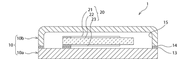
- FIG. 2 is a schematic cross-sectional view of an electronic component according to an embodiment of the present invention.
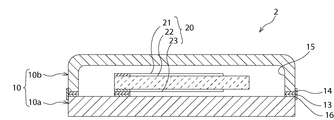
- FIG. 3 is a schematic cross-sectional view of an electronic component according to another embodiment of the present invention.
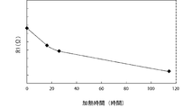
- FIG. 4 is a graph showing the relationship between the series resistance R1 of the piezoelectric vibrator and the heating time in Example 1.
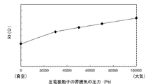
- FIG. 5 is a graph showing the relationship between the series resistance R1 of the piezoelectric vibrator and the pressure of the atmosphere in which the piezoelectric vibrator is arranged.
- the present invention is implemented by taking as an example the method of manufacturing the electronic component shown in FIGS.
- the method of manufacturing the electronic component shown in FIGS. 1 and 2 is merely an example.
- the present invention is not limited to the following electronic component manufacturing method.
- FIG. 1 is a schematic exploded perspective view of an electronic component according to this embodiment.
- FIG. 2 is a schematic cross-sectional view of the electronic component according to the present embodiment.
- the electronic component 1 includes a sealing member 10 and an electronic component main body 20.
- the sealing member 10 includes a first sealing member piece 10a, a second sealing member piece 10b, a resin layer 13, and an insulating layer 14.
- the first sealing member piece 10 a and the second sealing member piece 10 b define a sealing space 15.
- the material of the first sealing member piece 10a and the second sealing member piece 10b is not particularly limited as long as the material has low gas permeability. It is preferable that the 1st sealing member piece 10a and the 2nd sealing member piece 10b consist of a material whose gas permeability is lower than resin.
- each of the first sealing member piece 10a and the second sealing member piece 10b may be formed of, for example, a metal such as iron or aluminum, an alloy such as stainless steel, a ceramic such as alumina, or the like. it can.
- the 1st sealing member piece 10a and the 2nd sealing member piece 10b may consist of a different material, and may consist of the same material.
- the first sealing member piece 10a is made of ceramic and the second sealing member piece 10b is made of metal will be described.
- the shape of the first sealing member piece 10a and the second sealing member piece 10b is not particularly limited as long as the sealing space 15 can be formed.
- the first sealing member piece 10a may have a plate shape
- the second sealing member piece 10b may have a bowl shape having a recess.
- each of the 1st and 2nd sealing member pieces 10a and 10b may be formed integrally, and may be comprised by the aggregate
- the 1st sealing member piece 10a and the 2nd sealing member piece 10b may have functions other than the function which forms sealing space.
- the first sealing member piece 10 a also has a function as a substrate that supports the electronic component main body 20. That is, in this embodiment, the electronic component main body 20 is mounted on the first sealing member piece 10a.
- the first sealing member piece 10a also has a function of pulling out the electrode of the electronic component body 20 to the outside.
- the resin layer 13 has adhered the 1st sealing member piece 10a and the 2nd sealing member piece 10b.
- the resin layer 13 has a property that the gas permeability coefficient increases as the temperature increases.
- the resin layer 13 is preferably formed of, for example, an epoxy resin.
- the resin forming the resin layer 13 may be a thermosetting resin.
- the insulating layer 14 is disposed between the first sealing member piece 10a and the second sealing member piece 10b. Specifically, the insulating layer 14 is disposed between the resin layer 13 and the first sealing member piece 10a. The insulating layer 14 insulates the first sealing member piece 10a from the second sealing member piece 10b.
- the insulating layer 14 can be formed of, for example, an epoxy-based, silicon-based, urethane-based, or imide-based resin, glass, metal oxide, or the like. In this embodiment, since the first sealing member piece 10a has conductivity, it is preferable to provide the insulating layer 14. However, when the first sealing member piece 10a has insulating properties, the insulating layer 14 is provided. 14 is not necessarily essential.
- the electronic component body 20 is mounted on the first sealing member piece 10 a and is disposed inside the sealing space 15.
- the electronic component main body 20 is configured by a piezoelectric vibrator.
- the electronic component main body 20 is composed of a crystal resonator.
- the electronic component body is not necessarily a piezoelectric vibrator.
- the electronic component body may be, for example, an acoustic wave device such as a surface acoustic wave device.
- the electronic component main body 20 specifically includes a piezoelectric substrate 22 made of quartz and a pair of electrodes 21 and 23.
- the electrode 21 is formed on one main surface of the piezoelectric substrate 22, and the electrode 23 is formed on the other main surface of the piezoelectric substrate 22.
- a voltage is applied to the piezoelectric substrate 22 by these electrodes 21 and 23.
- the electrode 23 can be formed of, for example, a metal such as aluminum, silver, copper, or gold, or an alloy containing one or more of these metals.
- the electronic component main body 20 and the first sealing member piece 10a are prepared.
- the electronic component main body 20 is mounted on the first sealing member piece 10a.
- the electronic component body 20 can be mounted using, for example, a conductive adhesive or solder.
- a second sealing member piece 10b having the insulating layer 14 formed on the end surface is prepared.
- the second sealing member piece 10b is disposed on the first sealing member piece 10a.
- the first sealing member piece 10a and the second sealing member piece 10b are bonded with resin (bonding step).
- the atmosphere in which the bonding step is performed may be an air atmosphere or an inert gas atmosphere such as a nitrogen gas atmosphere or an argon gas atmosphere.
- the sealing member 10 is heated (heating process). Thereafter, the sealing member 10 is cooled (cooling step).
- the gas permeability coefficient of the resin layer 13 increases as the temperature increases, and decreases as the temperature decreases. For this reason, in the heating step, the gas permeability coefficient of the resin layer 13 increases, and the gas in the sealed space 15 expanded by being heated is released to the outside of the sealing member 10 via the resin layer 13. Is done.
- the subsequent cooling step since the gas permeability coefficient of the resin layer 13 is reduced, the inflow of gas through the resin layer 13 is suppressed, and the sealed space 15 is maintained in a reduced pressure atmosphere. As a result, the electronic component 1 in which the sealed space 15 is in a reduced pressure atmosphere can be completed.
- the said heating process in a pressure-reduced atmosphere.
- the air in the sealed space 15 can be efficiently discharged. Therefore, the internal pressure of the sealing space 15 can be reduced.
- the cooling step is also preferably performed in a reduced pressure atmosphere. By doing so, an increase in the internal pressure of the sealed space 15 in the cooling process can be suppressed.
- the heating temperature in the heating step is not particularly limited, but can be, for example, about 80 ° C. to 300 ° C. If the heating temperature is too low, the internal pressure of the sealed space 15 may not be sufficiently lowered. On the other hand, if the heating temperature is too high, the resin layer 13 deteriorates, the gas permeability coefficient of the resin layer 13 after cooling becomes high, and the sealed space 15 may not be formed suitably. Further, if the heating temperature is too high, the electronic component main body 20 may be damaged.
- the heating time in the heating step is not particularly limited, but can be, for example, about 10 hours to 150 hours.
- FIG. 3 is a schematic cross-sectional view of the electronic component 2 manufactured in the present embodiment.
- the electronic component 2 manufactured in the present embodiment has a configuration substantially similar to that of the electronic component 1 of the above-described embodiment except that the transmission suppressing layer 16 is provided.
- the permeation suppression layer 16 is formed so as to cover the outer periphery of the resin layer 13.
- the permeation suppression layer 16 is a layer having a gas permeability coefficient lower than that of the resin layer 13.
- the permeation suppression layer 16 can be formed of, for example, a metal film made of nickel, copper, tin, or the like.
- a step of forming the permeation suppression layer 16 after performing the cooling step is provided. For this reason, in the electronic component 2, the internal pressure of the sealing space 15 is unlikely to increase. That is, according to the present embodiment, it is possible to manufacture the electronic component 2 in which the internal pressure of the sealed space 15 is unlikely to increase.
- transmission suppression layer 16 is not specifically limited.
- the permeation suppression layer 16 is made of metal, the permeation suppression layer 16 can be formed by plating, for example.
- Example 1 a piezoelectric vibration device having a configuration substantially similar to that of the electronic component 1 shown in FIGS. 1 and 2 was produced in the following manner.
- the piezoelectric vibrator was mounted on an alumina support substrate as a first sealing member piece.
- a metal cap as a second sealing member piece made of nickel was bonded to the alumina support substrate using an epoxy resin adhesive.
- the series resistance R1 of the piezoelectric vibrator was measured.
- the sample prepared above was left in a vacuum oven at a temperature of 200 ° C. and an atmospheric pressure of 50 Pa for 115 hours. Thereafter, the sample was taken out of the vacuum oven and left in a normal temperature and atmospheric pressure atmosphere to cool the sample.
- the electronic component was completed by the above process.
- the series resistance R1 of the piezoelectric vibrator was measured. As a result, it was confirmed that the series resistance R1 was lowered by performing the heating step. From this result, it can be seen that the internal pressure of the sealed space can be reduced by performing the heating step and the cooling step.
- Example 2 An electronic component was manufactured in the same manner as in Example 1 except that the heating time was 16 hours, and the series resistance R1 of the piezoelectric vibrator was measured. The results are shown in FIG.
- Example 3 An electronic component was produced in the same manner as in Example 1 except that the heating time was 24 hours, and the series resistance R1 of the piezoelectric vibrator was measured. The results are shown in FIG.
Landscapes
- Physics & Mathematics (AREA)
- Acoustics & Sound (AREA)
- Piezo-Electric Or Mechanical Vibrators, Or Delay Or Filter Circuits (AREA)
Abstract
封止構造を有する電子部品を容易に製造することができる方法を提供する。 大気圧雰囲気中において、樹脂層13により第1の封止部材片10aと第2の封止部材片10bとを接着する。その後に、封止部材10内の気体が樹脂層13を経由して外部に放出されるように封止部材10を加熱する。その後に、封止部材10を冷却する。
Description
本発明は、電子部品の製造方法に関する。
従来、例えば水晶振動子を用いた水晶発振装置が知られている。下記の特許文献1~4に記載されているように、水晶発振装置では、一般的に、水晶振動子が封止空間内に配置されている。これにより、水晶振動子に加わる外乱の影響が小さくされている。
しかしながら、特許文献1,2に記載の水晶発振装置では、封止空間が減圧雰囲気にされていない。このため、水晶振動子の振動が封止空間内の気体によりダンピングされやすい。従って、水晶振動子の直列抵抗が上昇してしまうという問題がある。
それに対して、特許文献3,4に記載の水晶発振装置では、封止空間が減圧雰囲気にされている。このため、水晶振動子がダンピングされ難い。従って、水晶振動子の直列抵抗が上昇し難い。
なお、特許文献3,4には、封止空間が減圧雰囲気とされた水晶発振装置の製造方法として、水晶振動子を減圧雰囲気中において封止する方法が記載されている。
しかしながら、上記特許文献3,4に記載のように、水晶振動子を減圧雰囲気中において封止するためには、大がかりな装置が必要となる。このため、水晶発振装置の製造が困難になるばかりか、水晶発振装置の製造コストが上昇するという問題がある。
なお、このような問題は、水晶発振装置のみならず、封止構造を有する電子部品全般において共通の課題である。
本発明は、斯かる点に鑑みてなされたものであり、その目的は、封止構造を有する電子部品を容易に製造し得る方法を提供することにある。
本発明に係る電子部品の製造方法は、封止部材と、電子部品本体とを有する電子部品の製造方法に関する。封止部材は、第1及び第2の封止部材片と、樹脂層とを有している。第1の封止部材片と第2の封止部材片とは、互いに付き合わされている。第1の封止部材片と第2の封止部材片との間には、封止空間が形成されている。第1の封止部材片と第2の封止部材片とは、樹脂層により接着されている。電子部品本体は、封止空間内に配置されている。本発明に係る電子部品の製造方法は、接着工程と、加熱工程と、冷却工程とを備えている。接着工程では、大気圧雰囲気中において、樹脂により第1の封止部材片と第2の封止部材片とを接着する。加熱工程では、接着工程の後に、封止部材内の気体が樹脂層を経由して外部に放出されるように封止部材を加熱する。冷却工程では、加熱工程の後に、封止部材を冷却する。
本発明に係る電子部品の製造方法のある特定の局面では、樹脂層は、エポキシ系樹脂により形成されている。エポキシ系樹脂の気体透過係数は、温度上昇と共に大きく増大する。このため、樹脂層をエポキシ系樹脂により形成した場合、封止部材の温度が上昇すると、封止部材内の気体が樹脂層を経由してより効率的に外部に放出される。また、樹脂層が冷却された後は、樹脂層の気体透過係数が小さくなるため、樹脂層を経由して封止空間内に気体が流入することが効果的に抑制される。すなわち、封止空間の内圧が上昇しにくい電子部品を製造することができる。
本発明に係る電子部品の製造方法の他の特定の局面では、封止部材を、80℃以上に加熱する。
本発明に係る電子部品の製造方法の別の特定の局面では、冷却工程の後に、樹脂層よりも気体透過係数が低い層を、樹脂層を覆うように形成する。そうすることにより、樹脂層を経由して封止空間内に気体が流入することを抑制することができる。従って、封止部材の内圧が上昇し難い電子部品を製造することができる。
本発明に係る電子部品の製造方法のさらに他の特定の局面では、樹脂層よりも気体透過係数が低い層として、金属膜を形成する。なお、本発明において、金属膜には、合金からなる膜が含まれるものとする。
本発明に係る電子部品の製造方法のさらに別の特定の局面では、金属膜をめっきにより形成する。
本発明に係る電子部品の製造方法のまた他の特定の局面では、電子部品本体には、圧電振動子を用いる。
本発明に係る電子部品の製造方法のまた別の特定の局面では、圧電振動子は、水晶振動子である。水晶振動子の場合、内圧の特性への影響が大きく、本発明がより好適に適用される。
本発明に係る電子部品の製造方法のさらにまた別の特定の局面では、加熱工程を減圧雰囲気中で行う。そうすることにより、封止空間の内圧がより小さな電子部品の製造が可能になる。
本発明では、電子部品本体を大気圧雰囲気中において封止した後に、樹脂層を経由して封止部材内の気体を外部に放出させることにより、封止空間を減圧雰囲気とする。従って、大がかりな装置を用いることなく、封止構造を有する電子部品を容易に製造することができる。
以下、本発明を実施した好ましい形態について、図1及び図2に示す電子部品の製造方法を例に挙げて説明する。但し、図1及び図2に示す電子部品の製造方法は、単なる例示である。本発明は、下記の電子部品の製造方法に限定されない。
図1は、本実施形態に係る電子部品の略図的分解斜視図である。図2は、本実施形態に係る電子部品の略図的断面図である。まず、図1及び図2を参照しながら、本実施形態において製造する電子部品1の構成について説明する。
(封止部材10)
電子部品1は、封止部材10と、電子部品本体20を備えている。
電子部品1は、封止部材10と、電子部品本体20を備えている。
封止部材10は、第1の封止部材片10aと、第2の封止部材片10bと、樹脂層13と、絶縁層14とを備えている。
第1の封止部材片10aと第2の封止部材片10bとは、封止空間15を区画形成している。第1の封止部材片10a及び第2の封止部材片10bの材質は、気体透過性の低いものである限りにおいて特に限定されない。第1の封止部材片10a及び第2の封止部材片10bは、樹脂よりも気体透過性の低い材料からなることが好ましい。具体的には、第1の封止部材片10a及び第2の封止部材片10bのそれぞれは、例えば、鉄、アルミニウムなどの金属、ステンレスなどの合金、アルミナ等のセラミック等により形成することができる。なお、第1の封止部材片10aと、第2の封止部材片10bとは、異なる材質からなるものであってもよいし、同じ材質からなるものであってもよい。本実施形態では、第1の封止部材片10aがセラミックからなり、第2の封止部材片10bが金属からなる例について説明する。
第1の封止部材片10a及び第2の封止部材片10bの形状は、封止空間15を形成できるものである限りにおいて特に限定されない。このため、例えば、本実施形態のように、第1の封止部材片10aを板状とし、第2の封止部材片10bを、凹部を有する碗状としてもよい。また、第1及び第2の封止部材片10a、10bの両方を凹部を有する碗状としてもよい。また、第1及び第2の封止部材片10a、10bのそれぞれは、一体に形成されていてもよいし、複数の部材の集合体により構成されていてもよい。
なお、第1の封止部材片10a及び第2の封止部材片10bは、封止空間を形成する機能以外の機能を兼ね備えていてもよい。本実施形態では、第1の封止部材片10aは、電子部品本体20を支持する基板としての機能も有している。すなわち、本実施形態では、電子部品本体20は、第1の封止部材片10aの上に搭載されている。また、第1の封止部材片10aは、電子部品本体20の電極を外部に引き出す機能も兼ね備えている。
樹脂層13は、第1の封止部材片10aと第2の封止部材片10bとを接着している。本実施形態では、樹脂層13は、温度が高くなるに従って気体透過係数が大きくなる性質を有している。樹脂層13は、例えば、エポキシ系樹脂により形成されていることが好ましい。なお、樹脂層13を形成する樹脂は、熱硬化性樹脂であってもよい。
絶縁層14は、第1の封止部材片10aと第2の封止部材片10bとの間に配置されている。具体的には、絶縁層14は、樹脂層13と第1の封止部材片10aとの間に配置されている。この絶縁層14により第1の封止部材片10aと第2の封止部材片10bとが絶縁されている。絶縁層14は、例えば、エポキシ系、シリコン系、ウレタン系、イミド系の樹脂、ガラス、金属酸化物等により形成することができる。なお、本実施形態では、第1の封止部材片10aが導電性を有するため、絶縁層14を設けることが好ましいが、第1の封止部材片10aが絶縁性を有する場合は、絶縁層14は、必ずしも必須ではない。
(電子部品本体20)
電子部品本体20は、第1の封止部材片10aの上に搭載されており、封止空間15の内部に配置されている。本実施形態では、電子部品本体20は、圧電振動子により構成されている。具体的には、電子部品本体20は、水晶振動子により構成されている。但し、本発明において、電子部品本体は、圧電振動子である必要は必ずしもない。電子部品本体は、例えば、弾性表面波素子などの弾性波素子等であってもよい。
電子部品本体20は、第1の封止部材片10aの上に搭載されており、封止空間15の内部に配置されている。本実施形態では、電子部品本体20は、圧電振動子により構成されている。具体的には、電子部品本体20は、水晶振動子により構成されている。但し、本発明において、電子部品本体は、圧電振動子である必要は必ずしもない。電子部品本体は、例えば、弾性表面波素子などの弾性波素子等であってもよい。
本実施形態では、電子部品本体20は、具体的には、水晶からなる圧電基板22と、一対の電極21,23とを備えている。電極21は、圧電基板22の一主面の上に形成されており、電極23は、圧電基板22の他主面の上に形成されている。これら電極21,23により圧電基板22に電圧が印加される。なお、電極23は、例えば、アルミニウム、銀、銅、金等の金属や、これらの金属のうちの一種以上を含む合金等により形成することができる。
(電子部品1の製造方法)
次に、電子部品1の製造方法の一例について説明する。
次に、電子部品1の製造方法の一例について説明する。
まず、電子部品本体20と、第1の封止部材片10aとを用意する。次に、第1の封止部材片10aの上に電子部品本体20を実装する。電子部品本体20の実装は、例えば、導電性接着剤や半田等を用いて行うことができる。
次に、絶縁層14が端面の上に形成された第2の封止部材片10bを用意する。その第2の封止部材片10bを第1の封止部材片10aの上に配置する。そして、大気圧雰囲気中において、第1の封止部材片10aと、第2の封止部材片10bとを樹脂により接着する(接着工程)。なお、接着工程を行う雰囲気は、空気雰囲気であってもよいし、窒素ガス雰囲気やアルゴンガス雰囲気といった不活性ガス雰囲気であってもよい。
次に、封止部材10を加熱する(加熱工程)。その後、封止部材10を冷却する(冷却工程)。ここで、本実施形態では、樹脂層13の気体透過係数は、温度上昇と共に増大し、温度低下と共に小さくなる。このため、上記加熱工程において、樹脂層13の気体透過係数が増大し、加熱されることにより膨張した封止空間15内の気体が樹脂層13を経由して、封止部材10の外部に放出される。また、その後の冷却工程において、樹脂層13の気体透過係数が小さくなるため、樹脂層13を経由しての気体の流入が抑制され、封止空間15が減圧雰囲気に保持される。その結果、封止空間15が減圧雰囲気にされた電子部品1を完成させることができる。
なお、上記加熱工程は、減圧雰囲気中において行うことが好ましい。そうすることにより、封止空間15内の空気を効率的に排出させることができる。従って、封止空間15の内圧を小さくすることができる。また、冷却工程も、減圧雰囲気中で行うことが好ましい。そうすることにより、冷却工程における封止空間15の内圧の上昇を抑制することができる。
加熱工程における加熱温度は、特に限定されないが、例えば、80℃~300℃程度とすることができる。加熱温度が低すぎると、封止空間15の内圧が十分に低くならない場合がある。一方、加熱温度が高すぎると、樹脂層13が劣化し、冷却後の樹脂層13の気体透過係数が高くなってしまい、封止空間15が好適に形成できない場合がある。また、加熱温度が高すぎると、電子部品本体20が損傷する場合がある。
加熱工程における加熱時間は、特に限定されないが、例えば、10時間~150時間程度とすることができる。
以下、本発明を実施した好ましい形態の他の例について説明する。以下の説明において、上記第1の実施形態と実質的に共通の機能を有する部材を共通の符号で参照し、説明を省略する。
図3は、本実施形態において製造する電子部品2の略図的断面図である。図3に示すように、本実施形態において製造する電子部品2は、透過抑制層16を備えること以外は、上記実施形態の電子部品1と実質的に同様の構成を有する。
本実施形態において、透過抑制層16は、樹脂層13の外周を覆うように形成されている。透過抑制層16は、樹脂層13よりも気体透過係数が低い層である。透過抑制層16は、例えば、ニッケル、銅、スズ等からなる金属膜により形成することができる。
本実施形態の電子部品2を製造する際には、上記冷却工程を行った後に、透過抑制層16を形成する工程を備えている。このため、電子部品2では、封止空間15の内圧が上昇しにくい。すなわち、本実施形態によれば、封止空間15の内圧が上昇しにくい電子部品2を製造することができる。
なお、透過抑制層16の形成方法は特に限定されない。透過抑制層16が金属からなる場合は、透過抑制層16は、例えば、めっきにより形成することができる。
以下、具体的な実施例に基づいて、本発明についてさらに詳細に説明する。但し、以下の実施例は単なる例である。本発明は、以下の実施例に何ら限定されない。
(実施例1)
本実施例では、図1及び図2に示す電子部品1と実質的に同様の構成を有する圧電振動装置を、以下の要領で作製した。
本実施例では、図1及び図2に示す電子部品1と実質的に同様の構成を有する圧電振動装置を、以下の要領で作製した。
まず、圧電振動子を、第1の封止部材片としてのアルミナ支持基板の上に実装した。次に、大気中において、ニッケルからなる第2の封止部材片としての金属キャップをアルミナ支持基板にエポキシ系樹脂接着剤を用いて接着した。まず、この状態で圧電振動子の直列抵抗R1を測定した。
次に、温度200℃、気圧50Paの真空オーブン機の中に、上記作製のサンプルを115時間放置した。その後、サンプルを真空オーブン機から取り出し、常温、大気圧雰囲気下に放置することにより、サンプルを冷却した。以上の工程により電子部品を完成させた。
次に、完成した電子部品において、圧電振動子の直列抵抗R1を測定した。その結果、加熱工程を行うことにより直列抵抗R1が低くなっていることが確認された。この結果から、加熱工程及び冷却工程を行うことにより封止空間の内圧を低減できることが分かる。
(実施例2)
加熱時間を16時間としたこと以外は、上記実施例1と同様にして電子部品を作製し、圧電振動子の直列抵抗R1を測定した。結果を、図4に示す。
加熱時間を16時間としたこと以外は、上記実施例1と同様にして電子部品を作製し、圧電振動子の直列抵抗R1を測定した。結果を、図4に示す。
(実施例3)
加熱時間を24時間としたこと以外は、上記実施例1と同様にして電子部品を作製し、圧電振動子の直列抵抗R1を測定した。結果を図4に示す。
加熱時間を24時間としたこと以外は、上記実施例1と同様にして電子部品を作製し、圧電振動子の直列抵抗R1を測定した。結果を図4に示す。
図4に示す結果から、加熱時間を長くすることにより、封止空間の内圧をより低減できることが分かる。
なお、圧電振動子が配置された雰囲気の圧力が低くなるほど圧電振動子の直列抵抗R1が低くなることは、図5に示すグラフから明らかである。
1,2…電子部品
10…封止部材
10a…第1の封止部材片
10b…第2の封止部材片
13…樹脂層
14…絶縁層
15…封止空間
16…透過抑制層
20…電子部品本体
21,23…電極
22…圧電基板
10…封止部材
10a…第1の封止部材片
10b…第2の封止部材片
13…樹脂層
14…絶縁層
15…封止空間
16…透過抑制層
20…電子部品本体
21,23…電極
22…圧電基板
Claims (9)
- 互いに付き合わされた第1及び第2の封止部材片と、前記第1の封止部材片と前記第2の封止部材片とを接着している樹脂層とを有し、前記第1の封止部材片と前記第2の封止部材片との間に封止空間が形成された封止部材と、前記封止空間に配置された電子部品本体とを有する電子部品の製造方法であって、
大気圧雰囲気中において、前記樹脂により前記第1の封止部材片と前記第2の封止部材片とを接着する接着工程と、
前記接着工程の後に、前記封止部材内の気体が前記樹脂層を経由して外部に放出されるように前記封止部材を加熱する加熱工程と、
前記加熱工程の後に前記封止部材を冷却する冷却工程と、
を備える、電子部品の製造方法。 - 前記樹脂層を、エポキシ系樹脂により形成する、請求項1に記載の電子部品の製造方法。
- 前記封止部材を80℃以上に加熱する、請求項1または2に記載の電子部品の製造方法。
- 前記冷却工程の後に、前記樹脂層よりも気体透過係数が低い層を、前記樹脂層を覆うように形成する工程をさらに備える、請求項1~3のいずれか一項に記載の電子部品の製造方法。
- 前記樹脂層よりも気体透過係数が低い層として金属膜を形成する、請求項4に記載の電子部品の製造方法。
- 前記金属膜をめっきにより形成する、請求項5に記載の電子部品の製造方法。
- 前記電子部品本体として圧電振動子を用いる、請求項1~6のいずれか一項に記載の電子部品の製造方法。
- 前記圧電振動子が水晶振動子である、請求項7に記載の電子部品の製造方法。
- 前記加熱工程を、減圧雰囲気中で行う、請求項1~8のいずれか一項に記載の電子部品の製造方法。
Priority Applications (2)
| Application Number | Priority Date | Filing Date | Title |
|---|---|---|---|
| JP2012548698A JPWO2012081328A1 (ja) | 2010-12-16 | 2011-11-04 | 電子部品の製造方法 |
| CN2011800598857A CN103262235A (zh) | 2010-12-16 | 2011-11-04 | 电子部件的制造方法 |
Applications Claiming Priority (2)
| Application Number | Priority Date | Filing Date | Title |
|---|---|---|---|
| JP2010280766 | 2010-12-16 | ||
| JP2010-280766 | 2010-12-16 |
Publications (1)
| Publication Number | Publication Date |
|---|---|
| WO2012081328A1 true WO2012081328A1 (ja) | 2012-06-21 |
Family
ID=46244441
Family Applications (1)
| Application Number | Title | Priority Date | Filing Date |
|---|---|---|---|
| PCT/JP2011/075391 Ceased WO2012081328A1 (ja) | 2010-12-16 | 2011-11-04 | 電子部品の製造方法 |
Country Status (3)
| Country | Link |
|---|---|
| JP (1) | JPWO2012081328A1 (ja) |
| CN (1) | CN103262235A (ja) |
| WO (1) | WO2012081328A1 (ja) |
Families Citing this family (1)
| Publication number | Priority date | Publication date | Assignee | Title |
|---|---|---|---|---|
| CN116723664A (zh) * | 2023-06-25 | 2023-09-08 | 湖北星纪魅族科技有限公司 | 复合部件的密封方法、复合部件及电子设备 |
Citations (4)
| Publication number | Priority date | Publication date | Assignee | Title |
|---|---|---|---|---|
| JPH06188326A (ja) * | 1992-12-18 | 1994-07-08 | Mitsubishi Electric Corp | 樹脂シール中空型半導体装置及びその製造方法 |
| JPH09246867A (ja) * | 1996-03-11 | 1997-09-19 | Fujisawa Electron Kk | 表面実装形小型水晶発振器 |
| JP2006073679A (ja) * | 2004-08-31 | 2006-03-16 | Citizen Watch Co Ltd | 電子部品封止体の製造方法および製造装置 |
| JP2009182806A (ja) * | 2008-01-31 | 2009-08-13 | Kyocera Kinseki Corp | 圧電デバイス及びその製造方法 |
Family Cites Families (4)
| Publication number | Priority date | Publication date | Assignee | Title |
|---|---|---|---|---|
| JPS61248450A (ja) * | 1985-04-26 | 1986-11-05 | Hitachi Ltd | 半導体デバイスのパツケ−ジ封止構造 |
| EP0273556A1 (en) * | 1986-12-22 | 1988-07-06 | Trw Inc. | Integrated-circuit chip packaging construction |
| JP4290194B2 (ja) * | 2004-04-27 | 2009-07-01 | 中島硝子工業株式会社 | 太陽電池モジュールの製造方法 |
| JP2008112886A (ja) * | 2006-10-31 | 2008-05-15 | Epson Toyocom Corp | 電子部品収納用パッケージおよびこれを用いた電子デバイス |
-
2011
- 2011-11-04 CN CN2011800598857A patent/CN103262235A/zh active Pending
- 2011-11-04 JP JP2012548698A patent/JPWO2012081328A1/ja active Pending
- 2011-11-04 WO PCT/JP2011/075391 patent/WO2012081328A1/ja not_active Ceased
Patent Citations (4)
| Publication number | Priority date | Publication date | Assignee | Title |
|---|---|---|---|---|
| JPH06188326A (ja) * | 1992-12-18 | 1994-07-08 | Mitsubishi Electric Corp | 樹脂シール中空型半導体装置及びその製造方法 |
| JPH09246867A (ja) * | 1996-03-11 | 1997-09-19 | Fujisawa Electron Kk | 表面実装形小型水晶発振器 |
| JP2006073679A (ja) * | 2004-08-31 | 2006-03-16 | Citizen Watch Co Ltd | 電子部品封止体の製造方法および製造装置 |
| JP2009182806A (ja) * | 2008-01-31 | 2009-08-13 | Kyocera Kinseki Corp | 圧電デバイス及びその製造方法 |
Also Published As
| Publication number | Publication date |
|---|---|
| CN103262235A (zh) | 2013-08-21 |
| JPWO2012081328A1 (ja) | 2014-05-22 |
Similar Documents
| Publication | Publication Date | Title |
|---|---|---|
| JP5056837B2 (ja) | 圧電デバイスの製造方法 | |
| JP6247006B2 (ja) | 電子デバイス、発振器及び電子デバイスの製造方法 | |
| JP2014067849A (ja) | 電子デバイス用容器の製造方法、電子デバイスの製造方法、電子機器及び移動体機器 | |
| CN101807895A (zh) | 压电振子、压电振子的制造方法以及振荡器 | |
| CN102017132A (zh) | 气密密封用盖 | |
| JP6342643B2 (ja) | 電子デバイス | |
| KR102228131B1 (ko) | 전자 디바이스 및 전자 디바이스의 제조 방법 | |
| JP6488667B2 (ja) | 表面弾性波デバイス | |
| JP2019016737A (ja) | 電子部品およびその製造方法 | |
| WO2021186790A1 (ja) | 水晶振動素子、水晶振動子及び水晶発振器 | |
| WO2012081328A1 (ja) | 電子部品の製造方法 | |
| JP6230286B2 (ja) | 電子デバイス及び電子デバイスの製造方法 | |
| JP2009100213A (ja) | 圧電振動装置の製造方法 | |
| JP2015002414A (ja) | 電子デバイス | |
| JP2015018831A (ja) | 電子部品の気密封止方法 | |
| WO2018212184A1 (ja) | 圧電振動子の製造方法 | |
| JP2011066655A (ja) | 水晶振動素子 | |
| JP5093355B2 (ja) | 水晶発振装置 | |
| JP2014183359A (ja) | 水晶振動子 | |
| JP2010114132A5 (ja) | ||
| JP2013168863A (ja) | 電子部品 | |
| TWI559681B (zh) | 石英震盪器環壁結構之製造方法及製備而得之石英震盪器環壁結構 | |
| JP2014192539A (ja) | 圧電デバイス及びその製造方法 | |
| JP2014143559A (ja) | 電子デバイスの製造方法、電子デバイス及び発振器 | |
| JP2006311337A (ja) | 水晶振動子の励振電極構造、及びその製造方法 |
Legal Events
| Date | Code | Title | Description |
|---|---|---|---|
| 121 | Ep: the epo has been informed by wipo that ep was designated in this application |
Ref document number: 11849355 Country of ref document: EP Kind code of ref document: A1 |
|
| ENP | Entry into the national phase |
Ref document number: 2012548698 Country of ref document: JP Kind code of ref document: A |
|
| NENP | Non-entry into the national phase |
Ref country code: DE |
|
| 122 | Ep: pct application non-entry in european phase |
Ref document number: 11849355 Country of ref document: EP Kind code of ref document: A1 |