WO2012081213A1 - 表示装置の駆動装置、駆動方法、および表示装置システム - Google Patents
表示装置の駆動装置、駆動方法、および表示装置システム Download PDFInfo
- Publication number
- WO2012081213A1 WO2012081213A1 PCT/JP2011/006899 JP2011006899W WO2012081213A1 WO 2012081213 A1 WO2012081213 A1 WO 2012081213A1 JP 2011006899 W JP2011006899 W JP 2011006899W WO 2012081213 A1 WO2012081213 A1 WO 2012081213A1
- Authority
- WO
- WIPO (PCT)
- Prior art keywords
- voltage
- display device
- gradation
- reference voltage
- resistance connection
- Prior art date
- Legal status (The legal status is an assumption and is not a legal conclusion. Google has not performed a legal analysis and makes no representation as to the accuracy of the status listed.)
- Ceased
Links
Images




Classifications
-
- G—PHYSICS
- G09—EDUCATION; CRYPTOGRAPHY; DISPLAY; ADVERTISING; SEALS
- G09G—ARRANGEMENTS OR CIRCUITS FOR CONTROL OF INDICATING DEVICES USING STATIC MEANS TO PRESENT VARIABLE INFORMATION
- G09G3/00—Control arrangements or circuits, of interest only in connection with visual indicators other than cathode-ray tubes
- G09G3/20—Control arrangements or circuits, of interest only in connection with visual indicators other than cathode-ray tubes for presentation of an assembly of a number of characters, e.g. a page, by composing the assembly by combination of individual elements arranged in a matrix no fixed position being assigned to or needed to be assigned to the individual characters or partial characters
- G09G3/34—Control arrangements or circuits, of interest only in connection with visual indicators other than cathode-ray tubes for presentation of an assembly of a number of characters, e.g. a page, by composing the assembly by combination of individual elements arranged in a matrix no fixed position being assigned to or needed to be assigned to the individual characters or partial characters by control of light from an independent source
- G09G3/36—Control arrangements or circuits, of interest only in connection with visual indicators other than cathode-ray tubes for presentation of an assembly of a number of characters, e.g. a page, by composing the assembly by combination of individual elements arranged in a matrix no fixed position being assigned to or needed to be assigned to the individual characters or partial characters by control of light from an independent source using liquid crystals
- G09G3/3607—Control arrangements or circuits, of interest only in connection with visual indicators other than cathode-ray tubes for presentation of an assembly of a number of characters, e.g. a page, by composing the assembly by combination of individual elements arranged in a matrix no fixed position being assigned to or needed to be assigned to the individual characters or partial characters by control of light from an independent source using liquid crystals for displaying colours or for displaying grey scales with a specific pixel layout, e.g. using sub-pixels
-
- G—PHYSICS
- G09—EDUCATION; CRYPTOGRAPHY; DISPLAY; ADVERTISING; SEALS
- G09G—ARRANGEMENTS OR CIRCUITS FOR CONTROL OF INDICATING DEVICES USING STATIC MEANS TO PRESENT VARIABLE INFORMATION
- G09G3/00—Control arrangements or circuits, of interest only in connection with visual indicators other than cathode-ray tubes
- G09G3/20—Control arrangements or circuits, of interest only in connection with visual indicators other than cathode-ray tubes for presentation of an assembly of a number of characters, e.g. a page, by composing the assembly by combination of individual elements arranged in a matrix no fixed position being assigned to or needed to be assigned to the individual characters or partial characters
- G09G3/34—Control arrangements or circuits, of interest only in connection with visual indicators other than cathode-ray tubes for presentation of an assembly of a number of characters, e.g. a page, by composing the assembly by combination of individual elements arranged in a matrix no fixed position being assigned to or needed to be assigned to the individual characters or partial characters by control of light from an independent source
- G09G3/36—Control arrangements or circuits, of interest only in connection with visual indicators other than cathode-ray tubes for presentation of an assembly of a number of characters, e.g. a page, by composing the assembly by combination of individual elements arranged in a matrix no fixed position being assigned to or needed to be assigned to the individual characters or partial characters by control of light from an independent source using liquid crystals
- G09G3/3611—Control of matrices with row and column drivers
- G09G3/3696—Generation of voltages supplied to electrode drivers
-
- G—PHYSICS
- G09—EDUCATION; CRYPTOGRAPHY; DISPLAY; ADVERTISING; SEALS
- G09G—ARRANGEMENTS OR CIRCUITS FOR CONTROL OF INDICATING DEVICES USING STATIC MEANS TO PRESENT VARIABLE INFORMATION
- G09G2320/00—Control of display operating conditions
- G09G2320/02—Improving the quality of display appearance
- G09G2320/0252—Improving the response speed
-
- G—PHYSICS
- G09—EDUCATION; CRYPTOGRAPHY; DISPLAY; ADVERTISING; SEALS
- G09G—ARRANGEMENTS OR CIRCUITS FOR CONTROL OF INDICATING DEVICES USING STATIC MEANS TO PRESENT VARIABLE INFORMATION
- G09G2320/00—Control of display operating conditions
- G09G2320/02—Improving the quality of display appearance
- G09G2320/0271—Adjustment of the gradation levels within the range of the gradation scale, e.g. by redistribution or clipping
- G09G2320/0276—Adjustment of the gradation levels within the range of the gradation scale, e.g. by redistribution or clipping for the purpose of adaptation to the characteristics of a display device, i.e. gamma correction
-
- G—PHYSICS
- G09—EDUCATION; CRYPTOGRAPHY; DISPLAY; ADVERTISING; SEALS
- G09G—ARRANGEMENTS OR CIRCUITS FOR CONTROL OF INDICATING DEVICES USING STATIC MEANS TO PRESENT VARIABLE INFORMATION
- G09G2340/00—Aspects of display data processing
- G09G2340/16—Determination of a pixel data signal depending on the signal applied in the previous frame
Definitions
- the present invention relates to a driving device, a driving method, and a display device system for driving a display device such as a liquid crystal display device that performs gradation display.
- a driving device that drives a display device such as a liquid crystal display device includes a gradation voltage generation circuit that generates a plurality of types of gradation voltages, and a selector that selects any one of the gradation voltages according to a gradation data signal.
- a voltage corresponding to the gradation to be displayed is output.
- the gradation voltage generation circuit generates a plurality of kinds of gradation voltages by dividing a voltage between two reference voltages by a plurality of resistors connected in series. Further, in order to adjust the grayscale voltage generated by the grayscale voltage generation circuit to a desired voltage value, for example, about five of the connection points of the resistors in the plurality of resistors connected in series.
- the voltage at the connection point of the resistor to which the intermediate reference voltage is applied can be arbitrarily set.
- the rate of change that is, the change in voltage for each gradation, varies discontinuously. Therefore, for example, when the display gradation changes temporally or spatially with respect to the gradation corresponding to the connection point, there is a problem that the luminance changes unnaturally and the display image quality tends to deteriorate. It was.
- the present invention has been made in view of the above-described problem, and two reference voltages are applied to both ends of a plurality of resistors connected in series, and an intermediate reference voltage is applied to a connection point between the resistors.
- a display device driving device, a driving method, and a display device system in which a change in voltage for each gradation is suppressed to be small near a connection point to which the intermediate reference voltage is applied, and display image quality can be easily improved.
- the purpose is to provide.
- the first invention provides: A drive device for a display device that drives a display device by outputting a grayscale voltage according to a grayscale data signal, Having a plurality of resistors connected in series; The lowest reference voltage and the highest reference voltage are applied to both ends of the plurality of resistors, and an intermediate reference voltage is applied to at least one of the resistor connection points to which the resistors are connected.
- a smoothing circuit for smoothing a voltage between the resistance connection points is provided between resistance connection points located on both sides of the resistance connection point to which the intermediate reference voltage is applied.
- the second invention is A drive device for a display device according to a first invention
- the smoothing circuit is Two buffers for buffering voltages at two resistance connection points located on both sides of the resistance connection point to which the intermediate reference voltage is applied; A plurality of resistors for dividing the voltage between the output voltages of the two buffers to generate an intermediate voltage; It is characterized by having.
- the voltage at the resistance connection point near the resistance connection point to which the intermediate reference voltage is applied varies due to the influence of the current flowing through the resistor that generates the intermediate voltage. It can be set relatively easily.
- the third invention is A drive device for a display device according to any one of the first and second inventions,
- the smoothing circuit is A voltage dividing circuit that divides a voltage between two voltages to generate an intermediate voltage is provided in multiple stages.
- the fourth invention is: A drive device for a display device according to any one of the first to third inventions, A plurality of intermediate reference voltages are configured to be applied to a plurality of resistance connection points, The smoothing circuit is provided for each of the plurality of resistance connection points to which the intermediate reference voltage is applied.
- the fifth invention is: A drive device for a display device according to any one of the first to fourth inventions, A selector is provided for selecting one of the voltage at the resistor connection point and the output voltage of the smoothing circuit in accordance with a gradation data signal.
- the sixth invention is: A drive device for a display device according to any one of the first to fifth inventions, Further, the image processing apparatus further includes a gradation correction unit that outputs the gradation data signal corrected so as to emphasize gradation transition based on successive gradation data.
- the gradation correction unit includes a look-up table for obtaining corrected gradation data for representative gradations in successive gradation data, and gradation data other than the representative gradation is corrected by interpolation. It is characterized in that it is configured to obtain the gradation data.
- the eighth invention A display device driving method for driving a display device by outputting a gradation voltage according to a gradation data signal, Applying the lowest reference voltage and the highest reference voltage to both ends of a plurality of resistors connected in series, and applying an intermediate reference voltage to at least one of the resistance connection points to which the resistors are connected;
- a driving voltage for the display device is generated based on a voltage obtained by smoothing a voltage between resistance connection points located on both sides of the resistance connection point to which the intermediate reference voltage is applied.
- the ninth invention A display system, A drive device according to a first invention; A display device driven by the driving device; It is provided with.
- the tenth invention is A display device system according to a ninth invention,
- the display device is a liquid crystal display device.
- the present invention it is possible to easily improve the display image quality by suppressing a change in voltage for each gradation near a connection point to which an intermediate reference voltage is applied.
- FIG. 1 is a block diagram illustrating a schematic configuration of a liquid crystal display device according to an embodiment of the present invention.
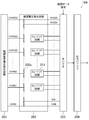
- 3 is a block diagram showing a detailed configuration of a source driver 104.
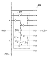
- FIG. 2 is a circuit diagram showing a detailed configuration of a gradation voltage generation circuit 202.
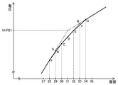
- FIG. It is a graph which shows a gradation-voltage characteristic. It is a graph which shows a gradation-voltage difference characteristic. It is explanatory drawing which shows the example of the lookup table for overdrive, and interpolation.
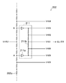
- FIG. 6 is a circuit diagram showing a modification of the gradation voltage generation circuit 202. It is a graph which shows the gradation-voltage characteristic of the gradation voltage generation circuit 202 of FIG.
- the liquid crystal display device includes a liquid crystal panel 101, a gate driver 102, a source driver 104 that is a driving device of the present invention, and a control unit 106.
- the gate driver 102 selects a display line by selectively activating a plurality of gate lines 103.
- the source driver 104 generates a voltage corresponding to the gradation data signal and applies it to each pixel of the display line selected by the gate driver 102 via the source line 105. Yes.
- the control unit 106 outputs a gradation data signal supplied to the source driver 104, a timing signal supplied to the gate driver 102, and the like.
- the source driver 104 includes, for example, a gradation reference voltage generation circuit 201 that generates reference voltages VHR0 to VHR255 for every 32 gradations, and a gradation voltage VH0 to 256 gradations based on the reference voltage.
- a gradation voltage generation circuit 202 that generates VH255, a selector 203 that selects any gradation voltage according to a gradation data signal, and an output buffer 204 that outputs the selected gradation voltage to the source line 105 with low impedance are provided. ing.
- the gradation voltage generation circuit 202 is provided with a series-connected voltage dividing resistor 202a for dividing a voltage between the reference voltages and a smoothing circuit 211. That is, for example, 255 voltage dividing resistors 202a are connected in series between the lowest and highest reference voltages VHR0 and VHR255. Further, intermediate reference voltages VHR31... Are connected to seven of the resistance connection points between the voltage dividing resistors 202a. The lowest and highest reference voltages VHR0 and VHR255 and some of the divided resistance connection points are output to the selector 203 as grayscale voltages VH0, VH1,... VH254, VH255, etc. The voltage divided in the vicinity of the resistance connection point to which the reference voltages VHR31, VHR63,... Are connected is input to the smoothing circuit 211.
- the smoothing circuit 211 further outputs a voltage between two voltages (A, B) divided by the voltage dividing resistor 202a near the resistance connection point to which the intermediate reference voltage is connected.
- An intermediate voltage (C, D, E) is generated by dividing by a voltage dividing resistor 211b via 211a, and output as gradation voltages VH30, VH31, VH32.
- the voltage between the voltage (C, E) divided by the voltage dividing resistor 211b and the voltage (F, G) divided by the voltage dividing resistor 202a are also respectively The voltage is divided to generate intermediate voltages (H, I) and output as gradation voltages VH29, VH33.
- the intermediate reference voltage VHR31 or the like in the present embodiment is not set so as to be output as a gradation voltage of 31 gradations or the like as it is, but is a voltage gradient between the smoothing circuits 211, that is, a portion that is not smoothed. Is set so that a desired gradation voltage is generated at 31 gradations to be smoothed or a gradation in the vicinity thereof.
- the smoothing circuit 211 By providing the smoothing circuit 211 as described above, the voltage difference for each gradation near the intermediate reference voltage is gradually made different as shown in FIGS. That is, when the smoothing circuit 211 is not used, as shown by a two-dot chain line in FIGS. 4 and 5, there is a voltage difference between adjacent gradations between 31 gradations and 31 gradations. It changes rapidly. On the other hand, by using the smoothing circuit 211 as in the present embodiment, the voltage difference between the adjacent gradations can be gradually changed from the 27th gradation to the 35th gradation.
- the image quality can be easily improved by using the smoothing circuit 211 as described above.
- overdrive driving that emphasizes gradation transition
- the effect of the overdrive driving is further increased.
- the control unit 106 sets the voltage actually applied to the source line 105 based on the previous frame gradation data and the current frame gradation data held in the frame memory.
- a gradation correction unit having a lookup table for determining corresponding gradation data is used. This lookup table is not normally set for all combinations of gradations, but is set for skipped representative gradations, for example, as shown in FIG. 6, and the intermediate gradations are obtained by linear interpolation or the like.
- the intermediate reference voltage VHR31 can be set from the outside of the grayscale voltage generation circuit 202, but at any previous frame and current frame grayscale data, as grayscale data for overdrive driving. It is difficult to set whether 31 gradations are determined.
- the smoothing circuit 211 as in the present embodiment, no matter what gradation is determined by linear interpolation as gradation data for overdrive driving, the voltage difference for each gradation gradually increases. In other words, since the generated gradation voltage becomes linear between any gradations, appropriate overdrive driving can be easily performed. Therefore, for example, even in the case of a liquid crystal display device for a three-dimensional television (3D TV) that requires particularly high-speed display, particularly fine voltage setting for overdrive driving is facilitated, high-speed response performance, and high image quality. Is easily obtained.
- FIG. 3 an example in which two-stage smoothing is performed as shown in FIG. 3 is shown.
- the voltage may be evenly divided between the VH 33 and the like.
- smoothing may be performed with three or more stages. That is, for example, when the voltage is divided and smoothed between the second and third voltage points on both sides of the first voltage point where the voltage gradient changes, the voltage gradient is also applied to the second and third voltage points. Since the voltage point changes, if the smoothing is further repeated for the voltage point, the degree of smoothing can be increased.
- smoothing of a plurality of types of stages may be mixed depending on the degree of change in voltage gradient for each gradation range.
- the number of smoothing stages may be different between the low voltage side and the high voltage side in one smoothing circuit.
- the buffer 211a is used as described above, an accurate voltage division ratio can be set relatively easily, but depending on the setting of the resistance values of the voltage dividing resistors 202a and 211b and the accuracy of the required gradation voltage.
- the buffer 211a is not necessarily used.
- the resistance values of the voltage dividing resistors 202a and 211b are not limited to each other, and may be set in accordance with the characteristics of the liquid crystal panel 101 as shown in Patent Document 1, for example.
- the example of the source driver 104 that generates a gradation voltage having a single polarity has been described.
- the present invention is not limited to this example.
- a source driver that generates a regulated voltage may be configured.
- the present invention is not limited to this, and the gradation reference voltage generation circuit 201 may be supplied from outside the source driver 104.
- the lookup table reference and interpolation are not limited to be performed in the control unit 106 but may be performed in the source driver 104.
- the present invention is useful for a driving device, a driving method, a display device system, and the like for driving a display device such as a liquid crystal display device that performs gradation display.
Landscapes
- Engineering & Computer Science (AREA)
- Chemical & Material Sciences (AREA)
- Crystallography & Structural Chemistry (AREA)
- Physics & Mathematics (AREA)
- Computer Hardware Design (AREA)
- General Physics & Mathematics (AREA)
- Theoretical Computer Science (AREA)
- Control Of Indicators Other Than Cathode Ray Tubes (AREA)
Abstract
スムージング回路(211)は、中間基準電圧が接続される抵抗接続点付近で分圧抵抗(202a)によって分圧された2つの電圧(A,B)間の電圧を、さらに、バッファ(211a)を介し分圧抵抗(211b)により分圧して中間の電圧(C,D,E)を発生し、階調電圧VH30,VH31,VH32として出力する。また、分圧抵抗(211b)によって分圧された電圧(C,E)と、分圧抵抗(202a)によって分圧された電圧(F,G)との間の電圧も、それぞれ、さらに分圧して中間の電圧(H,I)を発生し、階調電圧VH29,VH33として出力する。
Description
本発明は、階調表示を行う液晶表示装置等の表示装置を駆動する駆動装置、駆動方法、および表示装置システムに関する。
液晶表示装置等の表示装置を駆動する駆動装置は、複数種類の階調電圧を発生する階調電圧発生回路と、そのうち何れかの階調電圧を階調データ信号に応じて選択するセレクタとを備え、表示させる階調に応じた電圧を出力するようになっている。上記階調電圧発生回路は、直列に接続された複数の抵抗によって、2つの基準電圧間の電圧を分圧することにより、複数種類の階調電圧を発生するようになっている。また、階調電圧発生回路が発生する階調電圧が所望の電圧値に調整され得るようにするため、上記直列に接続された複数の抵抗における抵抗どうしの接続点のうち、例えば5箇所程度に中間の基準電圧が印加される技術が知られている(例えば、特許文献1(図3)参照)。これにより、上記中間の基準電圧が設定されることによって、階調電圧発生回路が発生する階調電圧が調整され、所望の階調表示特性が比較的容易に得られる。
しかしながら、上記のように中間の基準電圧が印加される場合、その中間の基準電圧が印加される抵抗の接続点の電圧自体は任意に設定され得るが、その抵抗の接続点の両側における電圧の変化率、すなわち1階調ごとの電圧の変化は不連続に異なることになる。そのため、例えば、表示階調が上記接続点に対応する階調を境に時間的または空間的に変化する場合に、輝度が不自然に変化し、表示画質が低下しがちであるという問題があった。
本発明は、上記の問題に鑑みてなされたものであり、直列に接続された複数の抵抗の両端に2つの基準電圧が印加され、抵抗どうしの接続点に中間の基準電圧が印加される場合に、上記中間の基準電圧が印加される接続点付近で1階調ごとの電圧の変化が小さく抑えられて、表示画質が容易に向上され得る表示装置の駆動装置、駆動方法、および表示装置システムを提供することを目的としている。
上記目的を達成するために、第1の発明は、
階調データ信号に従った階調電圧を出力して表示装置を駆動する表示装置の駆動装置であって、
直列に接続された複数の抵抗を有し、
上記複数の抵抗の両端に最低基準電圧と最高基準電圧とが印加されるとともに、抵抗どうしが接続される抵抗接続点のうち少なくとも1つの抵抗接続点に中間基準電圧が印加されるように構成され、
上記中間基準電圧が印加される抵抗接続点の両側に位置する抵抗接続点間に、上記抵抗接続点間の電圧をスムージングするスムージング回路が設けられていることを特徴とする。
階調データ信号に従った階調電圧を出力して表示装置を駆動する表示装置の駆動装置であって、
直列に接続された複数の抵抗を有し、
上記複数の抵抗の両端に最低基準電圧と最高基準電圧とが印加されるとともに、抵抗どうしが接続される抵抗接続点のうち少なくとも1つの抵抗接続点に中間基準電圧が印加されるように構成され、
上記中間基準電圧が印加される抵抗接続点の両側に位置する抵抗接続点間に、上記抵抗接続点間の電圧をスムージングするスムージング回路が設けられていることを特徴とする。
これにより、中間基準電圧が印加される抵抗接続点付近で1階調ごとの電圧の変化が小さく抑えられて、表示画質が容易に向上され得る。
第2の発明は、
第1の発明の表示装置の駆動装置であって、
上記スムージング回路は、
上記中間基準電圧が印加される抵抗接続点の両側に位置する2つの抵抗接続点の電圧をバッファリングする2つのバッファと、
上記2つのバッファの出力電圧間の電圧を分圧して中間の電圧を発生する複数の抵抗と、
を有することを特徴とする。
第1の発明の表示装置の駆動装置であって、
上記スムージング回路は、
上記中間基準電圧が印加される抵抗接続点の両側に位置する2つの抵抗接続点の電圧をバッファリングする2つのバッファと、
上記2つのバッファの出力電圧間の電圧を分圧して中間の電圧を発生する複数の抵抗と、
を有することを特徴とする。
これにより、中間基準電圧が印加される抵抗接続点付近の抵抗接続点の電圧が、上記中間の電圧を発生する抵抗に流れる電流の影響によって変動することが回避されるので、正確な分圧比が比較的容易に設定され得る。
第3の発明は、
第1および第2の発明のうち何れか1つの表示装置の駆動装置であって、
上記スムージング回路は、
2つの電圧間の電圧を分圧して中間の電圧を発生する分圧回路が多段に設けられていることを特徴とする。
第1および第2の発明のうち何れか1つの表示装置の駆動装置であって、
上記スムージング回路は、
2つの電圧間の電圧を分圧して中間の電圧を発生する分圧回路が多段に設けられていることを特徴とする。
これにより、1階調ごとの電圧の変化が一層小さく抑えられ得る。
第4の発明は、
第1から第3の発明のうち何れか1つの表示装置の駆動装置であって、
複数の中間基準電圧が複数の抵抗接続点に印加されるように構成され、
上記中間基準電圧が印加される複数の抵抗接続点に対応して、それぞれ上記スムージング回路が設けられていることを特徴とする。
第1から第3の発明のうち何れか1つの表示装置の駆動装置であって、
複数の中間基準電圧が複数の抵抗接続点に印加されるように構成され、
上記中間基準電圧が印加される複数の抵抗接続点に対応して、それぞれ上記スムージング回路が設けられていることを特徴とする。
これにより、広い階調範囲に亘って、上記スムージングの効果が得られる。
第5の発明は、
第1から第4の発明のうち何れか1つの表示装置の駆動装置であって、
階調データ信号に従って、上記抵抗接続点の電圧および上記スムージング回路の出力電圧のうち1つの電圧を選択するセレクタを備えたことを特徴とする。
第1から第4の発明のうち何れか1つの表示装置の駆動装置であって、
階調データ信号に従って、上記抵抗接続点の電圧および上記スムージング回路の出力電圧のうち1つの電圧を選択するセレクタを備えたことを特徴とする。
これにより、階調データ信号に従った適切な階調電圧が出力されるので、階調特性を容易に向上させることができる。
第6の発明は、
第1から第5の発明のうち何れか1つの表示装置の駆動装置であって、
さらに、相前後する階調データに基づいて、階調遷移を強調するように補正された上記階調データ信号を出力する階調補正部を備えたことを特徴とする。
第1から第5の発明のうち何れか1つの表示装置の駆動装置であって、
さらに、相前後する階調データに基づいて、階調遷移を強調するように補正された上記階調データ信号を出力する階調補正部を備えたことを特徴とする。
また、第7の発明は、
第6の発明の表示装置の駆動装置であって、
上記階調補正部は、相前後する階調データにおける代表階調に対して、補正された階調データを求めるルックアップテーブルを備え、代表階調以外の階調データについては、補間により、補正された階調データを求めるように構成されていることを特徴とする。
第6の発明の表示装置の駆動装置であって、
上記階調補正部は、相前後する階調データにおける代表階調に対して、補正された階調データを求めるルックアップテーブルを備え、代表階調以外の階調データについては、補間により、補正された階調データを求めるように構成されていることを特徴とする。
これらにより、オーバードライブ駆動についての特に細かな電圧設定が容易となり、高速な応答性能、および高い画質が容易に得られる。
第8の発明は、
階調データ信号に従った階調電圧を出力して表示装置を駆動する表示装置の駆動方法であって、
直列に接続された複数の抵抗の両端に最低基準電圧と最高基準電圧とを印加するとともに、抵抗どうしが接続される抵抗接続点のうち少なくとも1つの抵抗接続点に中間基準電圧を印加し、
上記中間基準電圧が印加される抵抗接続点の両側に位置する抵抗接続点間の電圧をスムージングして得られる電圧に基づいて、表示装置の駆動電圧を発生させることを特徴とする。
階調データ信号に従った階調電圧を出力して表示装置を駆動する表示装置の駆動方法であって、
直列に接続された複数の抵抗の両端に最低基準電圧と最高基準電圧とを印加するとともに、抵抗どうしが接続される抵抗接続点のうち少なくとも1つの抵抗接続点に中間基準電圧を印加し、
上記中間基準電圧が印加される抵抗接続点の両側に位置する抵抗接続点間の電圧をスムージングして得られる電圧に基づいて、表示装置の駆動電圧を発生させることを特徴とする。
これにより、上記のように、中間基準電圧が印加される抵抗接続点付近で1階調ごとの電圧の変化が小さく抑えられて、表示画質を向上させる駆動電圧が発生させられ得る。
第9の発明は、
表示装置システムであって、
第1の発明の駆動装置と、
上記駆動装置によって駆動される表示装置と、
を備えたことを特徴とする。
表示装置システムであって、
第1の発明の駆動装置と、
上記駆動装置によって駆動される表示装置と、
を備えたことを特徴とする。
第10の発明は、
第9の発明の表示装置システムであって、
上記表示装置が液晶表示装置であることを特徴とする。
第9の発明の表示装置システムであって、
上記表示装置が液晶表示装置であることを特徴とする。
これらにより、上記のように表示画質の高い表示装置システムを得ることが容易にできる。
本発明によれば、中間の基準電圧が印加される接続点付近で1階調ごとの電圧の変化を小さく抑えて、表示画質を容易に向上させることができる。
以下、本発明の実施形態を図面に基づいて詳細に説明する。なお、以下の実施形態および変形例において、他の図と同様の機能を有する構成要素については同一の符号を付して説明を省略する。
本発明の表示装置の駆動装置の例として、アクティブマトリクス型液晶表示装置に用いられるソースドライバについて説明する。上記液晶表示装置は、図1に示すように、液晶パネル101と、ゲートドライバ102と、本発明の駆動装置であるソースドライバ104と、コントロール部106とを備えている。上記ゲートドライバ102は、複数のゲートライン103を選択的にアクティブにすることによって、表示ラインを選択するようになっている。ソースドライバ104は、後に詳述するように階調データ信号に応じた電圧を発生し、ソースライン105を介して、上記ゲートドライバ102により選択された表示ラインの各画素に印加するようになっている。コントロール部106は、上記ソースドライバ104に供給する階調データ信号、およびゲートドライバ102に供給するタイミング信号等を出力するようになっている。
ソースドライバ104は、図2に示すように、例えば32階調ごとの基準電圧VHR0~VHR255を発生する階調基準電圧発生回路201、上記基準電圧を基にたとえば256階調の階調電圧VH0~VH255を発生する階調電圧発生回路202、階調データ信号に従って何れかの階調電圧を選択するセレクタ203、および選択された階調電圧を低インピーダンスでソースライン105に出力する出力バッファ204を備えている。
上記階調電圧発生回路202には、各基準電圧間の電圧を分圧する直列接続された分圧抵抗202aと、スムージング回路211とが設けられている。すなわち、最低、最高基準電圧VHR0,VHR255間に例えば255本の分圧抵抗202aが直列に接続されている。また、分圧抵抗202aどうしの抵抗接続点のうちの7箇所には、中間基準電圧VHR31…が接続されている。最低、最高基準電圧VHR0,VHR255と、分圧された抵抗接続点の電圧のうちの一部とは、そのまま階調電圧VH0,VH1,…VH254,VH255等としてセレクタ203に出力される一方、中間基準電圧VHR31,VHR63,…が接続される抵抗接続点付近で分圧された電圧は、スムージング回路211に入力されるようになっている。
スムージング回路211は、例えば図3に示すように、中間基準電圧が接続される抵抗接続点付近で分圧抵抗202aによって分圧された2つの電圧(A,B)間の電圧を、さらに、バッファ211aを介し分圧抵抗211bにより分圧して中間の電圧(C,D,E)を発生し、階調電圧VH30,VH31,VH32として出力するようになっている。また、同図の例では、分圧抵抗211bによって分圧された電圧(C,E)と、分圧抵抗202aによって分圧された電圧(F,G)との間の電圧も、それぞれ、さらに分圧して中間の電圧(H,I)を発生し、階調電圧VH29,VH33として出力するようになっている。
ここで、本実施形態における中間基準電圧VHR31等は、そのまま31階調等の階調電圧として出力されるように設定されるのではなく、各スムージング回路211間、すなわちスムージングされない部分での電圧勾配を所望にし、また、スムージングされる31階調またはその近辺の階調で所望の階調電圧が発生するように設定される。
上記のようなスムージング回路211が設けられることによって、図4、図5に示すように中間基準電圧付近の1階調ごとの電圧差が徐々に異なるようにされる。すなわち、スムージング回路211が用いられない場合には、図4、図5に2点鎖線で示すように、31以下の階調と31以上の階調とで、隣り合う階調との電圧差が急激に変化する。これに対し、本実施形態のようにスムージング回路211を用いることによって、27階調から35階調にかけて、隣り合う階調との電圧差が徐々に変化させられ得る。そこで、例えば隣接する画素の階調が31階調前後で少しずつ異なる場合や、1つの画素の階調が時間的に31階調の前後に亘って変化する場合に、不自然な輝度変化が容易に回避され、画質が向上させられ得る。特に、液晶パネル101の特性等に応じて中間基準電圧が種々に調整される場合でも、その中間基準電圧付近で確実にスムージング効果が得られる。しかも、階調電圧発生回路202内にスムージング回路211が設けられるだけでよく、液晶パネル101の駆動システム全体の構成に影響が与えられることがないので、製造コストの大幅な増加が招かれることもない。
また、上記のようにスムージング回路211が用いられることによって画質が容易に向上し得るが、さらに、階調遷移を強調するいわゆるオーバードライブ駆動が用いられる場合には、そのオーバードライブ駆動の効果がより適切に得られる。すなわち、オーバードライブ駆動においては、例えばコントロール部106において、フレームメモリに保持された前フレームの階調データと、現フレームの階調データとに基づいて、実際にソースライン105に印加される電圧に対応する階調データを決定するルックアップテーブル有する階調補正部が用いられる。このルックアップテーブルは、通常、全ての階調の組み合わせについては設定されず、例えば図6に示すように、飛び飛びの代表階調について設定され、間の階調については線形補間等により求められる。このため、例えば中間基準電圧VHR31は階調電圧発生回路202の外部から設定可能である一方、どのような前フレームおよび現フレームの階調データのときに、オーバードライブ駆動のための階調データとして31階調が決定されるかは設定が困難である。しかしながら、本実施形態のようにスムージング回路211が用いられることにより、どのような階調がオーバードライブ駆動のための階調データとして線形補間で決定されても、1階調ごとの電圧差は徐々に変化するので、すなわち発生する階調電圧が何れの階調間でも線形に近くなるので、適切なオーバードライブ駆動が容易に行われ得る。したがって、例えば、特に高速な表示が必要とされる3次元テレビ(3DTV)用液晶表示装置の場合などでも、オーバードライブ駆動についての特に細かな電圧設定が容易となり、高速な応答性能、および高い画質が容易に得られる。
なお、以上で説明したスムージング回路の階調数、スムージング精度は、一例であり、上記に限らず、種々変更されてもよい。
また、上記の例では、図3に示したように2段階のスムージングが行われる例を示したが、これに限らず、例えば図7、図8に示すように1段階のスムージング、すなわちVH29~VH33の間などで均等に分圧されるだけでもよい。一方、3段階以上の段数でスムージングされるようにしてもよい。すなわち、例えば、電圧勾配が変化する第1の電圧ポイントの両側の第2、第3の電圧ポイント間で分圧されてスムージングされる場合、上記第2、第3の電圧ポイントも、電圧勾配が変化する電圧ポイントとなるので、その電圧ポイントに対して、さらにスムージングが繰り返されれば、スムージング程度が高められ得る。また、階調範囲ごとの電圧勾配の変化程度に応じて、複数種類の段数のスムージングが混在するようにしてもよい。さらに、1つのスムージング回路内で低電圧側と高電圧側とでスムージング段数が異ならせられるなどしてもよい。
また、上記のようにバッファ211aが用いられれば、正確な分圧比の設定が比較的容易にできるが、分圧抵抗202a,211bの抵抗値の設定や必要とされる階調電圧の精度によっては、必ずしもバッファ211aが用いられなくてもよい。
また、分圧抵抗202a,211bの抵抗値は、互いに同一に限らず、例えば特許文献1に示されるのと同様に液晶パネル101の特性等に応じてそれぞれ設定されるようにしてもよい。
また、上記の例では、説明の便宜上、単一の極性の階調電圧を発生するソースドライバ104の例について説明したが、これに限るものではなく、いわゆる反転駆動のために正負の極性の階調電圧を発生するソースドライバが構成されてもよい。
また、階調基準電圧発生回路201はソースドライバ104内に設けられている例を示したが、これに限らず、ソースドライバ104の外部から供給されるなどしてもよい。
また、オーバードライブ駆動が行われる場合、ルックアップテーブルの参照や補間はコントロール部106内で行われるのに限らず、ソースドライバ104内で行われるなどしてもよい。
以上説明したように、本発明は、階調表示を行う液晶表示装置等の表示装置を駆動する駆動装置、駆動方法、および表示装置システム等に有用である。
101 液晶パネル
102 ゲートドライバ
103 ゲートライン
104 ソースドライバ
105 ソースライン
106 コントロール部
201 階調基準電圧発生回路
202 階調電圧発生回路
202a 分圧抵抗
203 セレクタ
204 出力バッファ
211 スムージング回路
211a バッファ
211b 分圧抵抗
102 ゲートドライバ
103 ゲートライン
104 ソースドライバ
105 ソースライン
106 コントロール部
201 階調基準電圧発生回路
202 階調電圧発生回路
202a 分圧抵抗
203 セレクタ
204 出力バッファ
211 スムージング回路
211a バッファ
211b 分圧抵抗
Claims (10)
- 階調データ信号に従った階調電圧を出力して表示装置を駆動する表示装置の駆動装置であって、
直列に接続された複数の抵抗を有し、
上記複数の抵抗の両端に最低基準電圧と最高基準電圧とが印加されるとともに、抵抗どうしが接続される抵抗接続点のうち少なくとも1つの抵抗接続点に中間基準電圧が印加されるように構成され、
上記中間基準電圧が印加される抵抗接続点の両側に位置する抵抗接続点間に、上記抵抗接続点間の電圧をスムージングするスムージング回路が設けられていることを特徴とする表示装置の駆動装置。 - 請求項1の表示装置の駆動装置であって、
上記スムージング回路は、
上記中間基準電圧が印加される抵抗接続点の両側に位置する2つの抵抗接続点の電圧をバッファリングする2つのバッファと、
上記2つのバッファの出力電圧間の電圧を分圧して中間の電圧を発生する複数の抵抗と、
を有することを特徴とする表示装置の駆動装置。 - 請求項1および請求項2のうち何れか1項の表示装置の駆動装置であって、
上記スムージング回路は、
2つの電圧間の電圧を分圧して中間の電圧を発生する分圧回路が多段に設けられていることを特徴とする表示装置の駆動装置。 - 請求項1から請求項3のうち何れか1項の表示装置の駆動装置であって、
複数の中間基準電圧が複数の抵抗接続点に印加されるように構成され、
上記中間基準電圧が印加される複数の抵抗接続点に対応して、それぞれ上記スムージング回路が設けられていることを特徴とする表示装置の駆動装置。 - 請求項1から請求項4のうち何れか1項の表示装置の駆動装置であって、
階調データ信号に従って、上記抵抗接続点の電圧および上記スムージング回路の出力電圧のうち1つの電圧を選択するセレクタを備えたことを特徴とする表示装置の駆動装置。 - 請求項1から請求項5のうち何れか1項の表示装置の駆動装置であって、
さらに、相前後する階調データに基づいて、階調遷移を強調するように補正された上記階調データ信号を出力する階調補正部を備えたことを特徴とする表示装置の駆動装置。 - 請求項6の表示装置の駆動装置であって、
上記階調補正部は、相前後する階調データにおける代表階調に対して、補正された階調データを求めるルックアップテーブルを備え、代表階調以外の階調データについては、補間により、補正された階調データを求めるように構成されていることを特徴とする表示装置の駆動装置。 - 階調データ信号に従った階調電圧を出力して表示装置を駆動する表示装置の駆動方法であって、
直列に接続された複数の抵抗の両端に最低基準電圧と最高基準電圧とを印加するとともに、抵抗どうしが接続される抵抗接続点のうち少なくとも1つの抵抗接続点に中間基準電圧を印加し、
上記中間基準電圧が印加される抵抗接続点の両側に位置する抵抗接続点間の電圧をスムージングして得られる電圧に基づいて、表示装置の駆動電圧を発生させることを特徴とする表示装置の駆動方法。 - 請求項1の駆動装置と、
上記駆動装置によって駆動される表示装置と、
を備えたことを特徴とする表示装置システム。 - 請求項9の表示装置システムであって、
上記表示装置が液晶表示装置であることを特徴とする表示装置システム。
Priority Applications (1)
| Application Number | Priority Date | Filing Date | Title |
|---|---|---|---|
| US13/994,528 US20130265344A1 (en) | 2010-12-17 | 2011-12-09 | Driving device, driving method, and system for display device |
Applications Claiming Priority (2)
| Application Number | Priority Date | Filing Date | Title |
|---|---|---|---|
| JP2010281259 | 2010-12-17 | ||
| JP2010-281259 | 2010-12-17 |
Publications (1)
| Publication Number | Publication Date |
|---|---|
| WO2012081213A1 true WO2012081213A1 (ja) | 2012-06-21 |
Family
ID=46244332
Family Applications (1)
| Application Number | Title | Priority Date | Filing Date |
|---|---|---|---|
| PCT/JP2011/006899 Ceased WO2012081213A1 (ja) | 2010-12-17 | 2011-12-09 | 表示装置の駆動装置、駆動方法、および表示装置システム |
Country Status (2)
| Country | Link |
|---|---|
| US (1) | US20130265344A1 (ja) |
| WO (1) | WO2012081213A1 (ja) |
Families Citing this family (5)
| Publication number | Priority date | Publication date | Assignee | Title |
|---|---|---|---|---|
| KR101975538B1 (ko) * | 2012-11-07 | 2019-05-08 | 삼성디스플레이 주식회사 | 유기전계 발광 표시장치의 계조전압 생성장치 |
| CN103680448B (zh) * | 2013-12-11 | 2015-07-01 | 深圳市华星光电技术有限公司 | 计算过驱动目标值的方法 |
| KR20160148937A (ko) * | 2015-06-17 | 2016-12-27 | 에스케이하이닉스 주식회사 | 반도체 장치의 기준전압 발생 장치 |
| US10249245B1 (en) | 2017-11-22 | 2019-04-02 | Shenzhen China Star Optoelectronics Semiconductor Display Technology Co., Ltd. | Compensation system and compensation method for AMOLED |
| CN107845365B (zh) * | 2017-11-22 | 2019-12-06 | 深圳市华星光电半导体显示技术有限公司 | Amoled显示器的补偿系统及补偿方法 |
Citations (4)
| Publication number | Priority date | Publication date | Assignee | Title |
|---|---|---|---|---|
| JPH09198012A (ja) * | 1996-01-24 | 1997-07-31 | Hitachi Ltd | 液晶表示装置 |
| JP2003316333A (ja) * | 2002-04-25 | 2003-11-07 | Sharp Corp | 表示駆動装置およびそれを用いた表示装置 |
| JP2004004629A (ja) * | 2002-03-25 | 2004-01-08 | Sharp Corp | 液晶表示装置 |
| JP2007179016A (ja) * | 2005-12-27 | 2007-07-12 | Samsung Electronics Co Ltd | ガンマ調整回路及びガンマ調整方法 |
Family Cites Families (1)
| Publication number | Priority date | Publication date | Assignee | Title |
|---|---|---|---|---|
| JP2002175060A (ja) * | 2000-09-28 | 2002-06-21 | Sharp Corp | 液晶駆動装置およびそれを備えた液晶表示装置 |
-
2011
- 2011-12-09 WO PCT/JP2011/006899 patent/WO2012081213A1/ja not_active Ceased
- 2011-12-09 US US13/994,528 patent/US20130265344A1/en not_active Abandoned
Patent Citations (4)
| Publication number | Priority date | Publication date | Assignee | Title |
|---|---|---|---|---|
| JPH09198012A (ja) * | 1996-01-24 | 1997-07-31 | Hitachi Ltd | 液晶表示装置 |
| JP2004004629A (ja) * | 2002-03-25 | 2004-01-08 | Sharp Corp | 液晶表示装置 |
| JP2003316333A (ja) * | 2002-04-25 | 2003-11-07 | Sharp Corp | 表示駆動装置およびそれを用いた表示装置 |
| JP2007179016A (ja) * | 2005-12-27 | 2007-07-12 | Samsung Electronics Co Ltd | ガンマ調整回路及びガンマ調整方法 |
Also Published As
| Publication number | Publication date |
|---|---|
| US20130265344A1 (en) | 2013-10-10 |
Similar Documents
| Publication | Publication Date | Title |
|---|---|---|
| JP5410731B2 (ja) | バックライトの輝度抑制の制御方法及びその制御方法を用いたディスプレイシステム | |
| JP5449404B2 (ja) | 表示装置 | |
| JP5079017B2 (ja) | 表示装置 | |
| KR20210082855A (ko) | 무라 보상 회로 및 그를 채용한 디스플레이를 위한 구동 장치 | |
| CN1954352A (zh) | 伽马校正电路、显示屏及具备它们的显示装置 | |
| WO2012081213A1 (ja) | 表示装置の駆動装置、駆動方法、および表示装置システム | |
| CN101101425B (zh) | 显示装置及其驱动方法 | |
| JP2009098355A (ja) | 駆動回路装置 | |
| TWI352955B (ja) | ||
| CN101556759A (zh) | 伽马校正装置及方法 | |
| CN113808550A (zh) | 可应用于在显示模块中进行亮度增强的设备 | |
| WO2013161648A1 (ja) | 表示制御回路、それを備えた液晶表示装置、および表示制御方法 | |
| CN101017650A (zh) | 用于驱动液晶显示器件的装置及其方法 | |
| WO2008032480A1 (en) | Liquid crystal driving circuit, driving method, and liquid crystal display apparatus | |
| US9640105B2 (en) | Signal processing method, display device, and electronic apparatus | |
| JP5895150B2 (ja) | 画像表示装置 | |
| JP2009008958A (ja) | 液晶表示駆動回路 | |
| CN101325044B (zh) | 用于帧升频转换的帧内插方法 | |
| TWI413976B (zh) | 過驅動系統、顯示系統及其過驅動方法 | |
| US8803774B2 (en) | Liquid crystal display and processing method thereof | |
| JP5095181B2 (ja) | 画像処理装置、液晶表示装置および画像処理装置の制御方法 | |
| US20040227712A1 (en) | Image processing method, image processing apparatus, and liquid crystal display using same | |
| US20070013717A1 (en) | Displaying non-linear images on linear displays | |
| JP5596477B2 (ja) | 表示パネルの駆動装置 | |
| JP7702751B2 (ja) | パネル駆動回路 |
Legal Events
| Date | Code | Title | Description |
|---|---|---|---|
| 121 | Ep: the epo has been informed by wipo that ep was designated in this application |
Ref document number: 11849291 Country of ref document: EP Kind code of ref document: A1 |
|
| WWE | Wipo information: entry into national phase |
Ref document number: 13994528 Country of ref document: US |
|
| NENP | Non-entry into the national phase |
Ref country code: DE |
|
| 122 | Ep: pct application non-entry in european phase |
Ref document number: 11849291 Country of ref document: EP Kind code of ref document: A1 |
|
| NENP | Non-entry into the national phase |
Ref country code: JP |