WO2012081161A1 - 半導体ウェーハの洗浄方法 - Google Patents
半導体ウェーハの洗浄方法 Download PDFInfo
- Publication number
- WO2012081161A1 WO2012081161A1 PCT/JP2011/006107 JP2011006107W WO2012081161A1 WO 2012081161 A1 WO2012081161 A1 WO 2012081161A1 JP 2011006107 W JP2011006107 W JP 2011006107W WO 2012081161 A1 WO2012081161 A1 WO 2012081161A1
- Authority
- WO
- WIPO (PCT)
- Prior art keywords
- cleaning
- semiconductor wafer
- wafer
- hydrofluoric acid
- cleaned
- Prior art date
- Legal status (The legal status is an assumption and is not a legal conclusion. Google has not performed a legal analysis and makes no representation as to the accuracy of the status listed.)
- Ceased
Links
Images

Classifications
-
- H—ELECTRICITY
- H10—SEMICONDUCTOR DEVICES; ELECTRIC SOLID-STATE DEVICES NOT OTHERWISE PROVIDED FOR
- H10P—GENERIC PROCESSES OR APPARATUS FOR THE MANUFACTURE OR TREATMENT OF DEVICES COVERED BY CLASS H10
- H10P70/00—Cleaning of wafers, substrates or parts of devices
-
- H—ELECTRICITY
- H10—SEMICONDUCTOR DEVICES; ELECTRIC SOLID-STATE DEVICES NOT OTHERWISE PROVIDED FOR
- H10P—GENERIC PROCESSES OR APPARATUS FOR THE MANUFACTURE OR TREATMENT OF DEVICES COVERED BY CLASS H10
- H10P70/00—Cleaning of wafers, substrates or parts of devices
- H10P70/10—Cleaning before device manufacture, i.e. Begin-Of-Line process
- H10P70/15—Cleaning before device manufacture, i.e. Begin-Of-Line process by wet cleaning only
-
- H—ELECTRICITY
- H10—SEMICONDUCTOR DEVICES; ELECTRIC SOLID-STATE DEVICES NOT OTHERWISE PROVIDED FOR
- H10P—GENERIC PROCESSES OR APPARATUS FOR THE MANUFACTURE OR TREATMENT OF DEVICES COVERED BY CLASS H10
- H10P70/00—Cleaning of wafers, substrates or parts of devices
- H10P70/20—Cleaning during device manufacture
-
- H—ELECTRICITY
- H10—SEMICONDUCTOR DEVICES; ELECTRIC SOLID-STATE DEVICES NOT OTHERWISE PROVIDED FOR
- H10P—GENERIC PROCESSES OR APPARATUS FOR THE MANUFACTURE OR TREATMENT OF DEVICES COVERED BY CLASS H10
- H10P72/00—Handling or holding of wafers, substrates or devices during manufacture or treatment thereof
- H10P72/04—Apparatus for manufacture or treatment
- H10P72/0402—Apparatus for fluid treatment
- H10P72/0406—Apparatus for fluid treatment for cleaning followed by drying, rinsing, stripping, blasting or the like
- H10P72/0411—Apparatus for fluid treatment for cleaning followed by drying, rinsing, stripping, blasting or the like for wet cleaning or washing
Definitions
- the present invention relates to an improvement in a method for cleaning a semiconductor wafer.
- a mixed cleaning solution of ammonia water, hydrogen peroxide solution and ultrapure water hereinafter referred to as SC1 (Standard Cleaning 1) cleaning solution
- SC2 Standard Cleaning 2 cleaning solution
- one of the improvement quality requirements accompanying the miniaturization of device design rules is a reduction in wafer surface roughness.
- the surface roughness of the wafer is usually formed by finish polishing, but the surface roughness of the wafer deteriorates as the etching allowance (etching amount) increases due to the etching action on the wafer (silicon) subjected to SC1 cleaning. It is known that when the surface roughness is deteriorated, the electrical characteristics of the oxide film formed on the silicon wafer are deteriorated, or the particle detection of the particle counter using laser light scattering is adversely affected. There is a demand to make the surface roughness as small as possible.
- the etching amount of SC1 cleaning is reduced in order to improve the wafer surface roughness, the cleaning power is reduced and particles remain. Therefore, in order to compensate for the reduction in the cleaning power due to the reduction in the etching amount, the amount of etching with the SC1 cleaning liquid can be reduced to some extent by enhancing the physical cleaning using ultrasonic waves used in the SC1 cleaning to improve the particle removal capability. You can now remove particles. However, when the etching amount by SC1 is 2.0 nm or less, there is a problem that particles cannot be removed even if the ultrasonic wave is improved.
- the present invention has been made in view of the above problems, and provides a semiconductor wafer cleaning method capable of reducing the deterioration of the wafer surface roughness due to cleaning and effectively cleaning the wafer. For the purpose.
- the present invention provides a method for cleaning a semiconductor wafer, the step of cleaning the semiconductor wafer with an SC1 cleaning solution, and the step of cleaning the semiconductor wafer cleaned with the SC1 cleaning solution with hydrofluoric acid. And a step of cleaning the semiconductor wafer cleaned with hydrofluoric acid with ozone water having an ozone concentration of 3 ppm or more, and an etching allowance of the semiconductor wafer with the SC1 cleaning solution is set to 0.1 to 2.0 nm.
- a method for cleaning a semiconductor wafer is provided.
- the cleaning with the SC1 cleaning liquid is performed with the etching allowance reduced to 0.1 to 2.0 nm, so that the deterioration of the surface roughness of the semiconductor wafer can be prevented. it can.
- Residual particles remaining after SC1 cleaning are removed by subsequent cleaning with hydrofluoric acid, and subsequent cleaning with ozone water with an ozone concentration of 3 ppm or more is used to attach an oxide film to the wafer surface to change the wafer surface from a hydrophobic surface to a hydrophilic surface.
- the reattachment of particles can be suppressed, the deterioration of the surface roughness of the wafer due to cleaning can be reduced, and the wafer can be cleaned effectively.
- the deterioration of the surface roughness of the wafer due to the cleaning can be reduced and the wafer can be effectively cleaned.
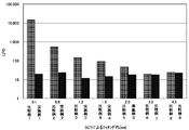
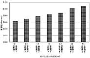
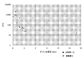
- 6 shows particle measurement results on wafer surfaces in Examples 1 to 5 and Comparative Examples 1 to 9. 6 is a result of measuring the surface roughness of the wafers in Examples 1 to 5 and Comparative Examples 1 to 9. It is a particle measurement result in Example 6 and Comparative Example 10.
- a method for cleaning a semiconductor wafer, the step of cleaning the semiconductor wafer with an SC1 cleaning solution, and the step of cleaning the semiconductor wafer cleaned with the SC1 cleaning solution with hydrofluoric acid And a step of cleaning the semiconductor wafer cleaned with hydrofluoric acid with ozone water having an ozone concentration of 3 ppm or more, and an etching allowance of the semiconductor wafer with the SC1 cleaning solution is set to 0.1 to 2.0 nm. It has been found that the semiconductor wafer cleaning method can reduce the deterioration of the surface roughness of the wafer due to the cleaning and can effectively clean the wafer.
- FIG. 1 is a flowchart for explaining an example of a semiconductor wafer cleaning method of the present invention. As shown in FIG. 1, the entire cleaning process is roughly divided into three stages: (A) a process of cleaning with SC1 cleaning liquid, (B) a process of cleaning with hydrofluoric acid, and (C) a process of cleaning with ozone water.
- the etching allowance of the semiconductor wafer is set to 0.1 to 2.0 nm by the SC1 cleaning liquid which is a mixed cleaning liquid of ammonia water, hydrogen peroxide water and ultrapure water.
- the semiconductor wafer is cleaned (FIG. 1A). Note that the etching allowance of the semiconductor wafer can be adjusted within the above range by changing the mixing ratio (volume ratio) of SC1 cleaning liquid, temperature, cleaning time, and the like.
- the temperature is 25 to 65 ° C.
- the mixing ratio is ammonia (NH 3 concentration 28%), hydrogen peroxide water (H 2 O 2 concentration 30%), the mixing ratio of water is 1: 1: 5 to 20, and the time is The conditions may be adjusted within the range of 180 to 360 seconds.
- cleaned in this invention The silicon wafer etc. after a normal grinding
- the etching allowance of the semiconductor wafer exceeds 2.0 nm, the surface roughness of the wafer deteriorates.
- the electrical properties of the oxide film formed on the silicon wafer deteriorate, or the particle counter using laser light scattering Adversely affects particle detection.
- the etching allowance of the semiconductor wafer is less than 0.1 nm, the particle removal effect cannot be obtained sufficiently.
- the conventional method for cleaning a semiconductor wafer has a problem that particles cannot be removed even if the ultrasonic wave is improved if the etching amount by the SC1 cleaning solution is 2.0 nm or less.
- the problem of remaining particles that occurs when the etching allowance with the SC1 cleaning solution is 2.0 nm or less is also caused by the (B) cleaning step with hydrofluoric acid described later. Can be solved.
- (B) a step of cleaning the semiconductor wafer cleaned with the SC1 cleaning solution with hydrofluoric acid is performed (FIG. 1B).
- the etching allowance with the SC1 cleaning solution is 2.0 nm or less, there is a problem that particles cannot be removed even if the physical cleaning with ultrasonic waves is strengthened. The remaining particles are strongly associated with the oxide film on the wafer surface formed in the SC1 cleaning process. Therefore, in the method for cleaning a semiconductor wafer according to the present invention, (B) hydrofluoric acid cleaning (HF cleaning) is added after (A) SC1 cleaning step to remove all oxide films formed in (A) SC1 cleaning step.
- HF cleaning hydrofluoric acid cleaning
- the concentration of hydrofluoric acid used is preferably 0.5 to 3.0%, the temperature is preferably 10 to 30 ° C., and the preferred washing time is 60 to 180 seconds.
- (C) a step of cleaning the semiconductor wafer cleaned with hydrofluoric acid with ozone water having an ozone concentration of 3 ppm or more is performed (FIG. 1C).
- the surface of the semiconductor wafer becomes a hydrophobic surface and particles are likely to adhere. Therefore, (B) a cleaning process with hydrofluoric acid, and (C) a cleaning process with ozone water having an ozone concentration of 3 ppm or more, that is, rinsing ozone water with an ozone concentration of 3 ppm or more in the rinsing tank, so that a silicon wafer can be obtained in a short time.
- An oxide film can be attached to the surface to form a hydrophilic surface, and reattachment of particles can be suppressed.
- the temperature of the ozone water used is preferably 10 to 30 ° C., and the preferred cleaning time is 60 to 180 seconds.
- the deterioration of the surface roughness can be suppressed (for example, the surface roughness Rms (Root Mean Square roughness) can be 0.1 nm or less), and The particles on the wafer surface can be effectively removed.
- the surface roughness Rms Root Mean Square roughness
- the semiconductor wafer may be cleaned with ozone water before the step of cleaning with the SC1 cleaning solution.
- ozone water By cleaning with ozone water in this way, organic substances can be effectively removed, and the cleaning effect is further enhanced. Further, rinsing with ultrapure water or the like may be appropriately performed between the cleaning steps (A), (B), and (C).
- Examples 1 to 5 In cleaning to remove the polishing agent etc. on the silicon wafer surface after mirror polishing, first cleaning with SC1 cleaning liquid, rinsing with ultrapure water, then HF cleaning and cleaning with ozone water continuously, finally The cleaned silicon wafer was dried.
- the temperature of the cleaning liquid is changed to change the etching allowance with the SC1 cleaning liquid to 0.1 to 2.0 nm (0.1, 0.6, 1.2, 1.6, 2.0 (Examples 1 to 5)).
- the SC1 cleaning solution used was a mixed cleaning solution in which the mixing ratio of ammonia, hydrogen peroxide solution, and water was 1: 1: 10.
- the HF concentration was 1.5% and the ozone concentration of ozone water was 17 ppm.
- Table 1 shows a summary of the particle measurement results and surface roughness results on the silicon wafer surface. From the above results, it was found that according to the semiconductor wafer cleaning method of the present invention, the deterioration of the surface roughness of the wafer due to the cleaning can be reduced and the wafer can be effectively cleaned (Example 1). ⁇ 5).
- Example 6 Comparative Example 10
- the silicon wafer after mirror polishing is subjected to SC1 cleaning with an etching allowance of 0.6 nm, followed by cleaning with hydrofluoric acid, and after cleaning with hydrofluoric acid, the ozone water concentration in the rinsing tank is swung from 0 to 2.8 ppm. And dried (Comparative Example 10). Further, the silicon wafer after mirror polishing was subjected to SC1 cleaning with an etching allowance of 0.6 nm, followed by cleaning with hydrofluoric acid, and after the hydrofluoric acid cleaning, the ozone water concentration in the rinsing tank was shaken to 3.0 to 17 ppm. Washing and drying were carried out (Example 6).
- the wafer particles after cleaning were measured with a wafer surface inspection device.
- the SC1 cleaning solution used in Example 6 and Comparative Example 10 was a mixed cleaning solution in which the mixing ratio of ammonia, hydrogen peroxide solution, and water was 1: 1: 10, and the hydrofluoric acid concentration was 1.5%.
- the results are shown in FIG.
- the ozone concentration of ozone water is 3 ppm or more (Example 6)
- the surface of the silicon wafer can be oxidized in a short time, that is, the hydrophobic surface can be changed to the hydrophilic surface. It turns out that it is stable.
- the present invention is not limited to the above embodiment.
- the above-described embodiment is an exemplification, and the present invention has any configuration that has substantially the same configuration as the technical idea described in the claims of the present invention and that exhibits the same effects. Are included in the technical scope.
Landscapes
- Cleaning Or Drying Semiconductors (AREA)
- Weting (AREA)
Abstract
Description
表面粗さが悪化すると、シリコンウェーハ上に形成される酸化膜の電気特性を悪化させたり、レーザー光の散乱を用いたパーティクルカウンターのパーティクル検出に悪影響を与えることが知られているため、ウェーハの表面粗さをできるだけ小さくすることが求められている。
前述のように、従来、洗浄によるウェーハの表面粗さの悪化を低減し、かつ、効果的にウェーハの洗浄を行うことができる半導体ウェーハの洗浄方法が求められていた。
図1に示すように、全体の洗浄工程は大きく(A)SC1洗浄液により洗浄する工程、(B)フッ酸により洗浄する工程、(C)オゾン水により洗浄する工程の3段階に区分される。
尚、SC1洗浄液の混合比(体積比)、温度、洗浄時間等を変更することにより、半導体ウェーハのエッチング代を上記範囲内に調整することが可能である。例えば、温度は25~65℃、混合比はアンモニア(NH3濃度28%)、過酸化水素水(H2O2濃度30%)、水の混合比で1:1:5~20、時間は180~360秒の範囲内で条件を調整すれば良い。
本発明において洗浄する半導体ウェーハとしては、特に限定されないが、通常研磨後のシリコンウェーハ等が挙げられる。
前述のように、従来の洗浄方法では、SC1洗浄液によるエッチング代が2.0nm以下である場合、超音波による物理洗浄を強化しても、パーティクルが除去できず残ってしまうという問題があった。この残ったパーティクルは、SC1洗浄工程で形成されるウェーハ表面の酸化膜と強く結びついている。そこで、本発明の半導体ウェーハの洗浄方法では、(A)SC1洗浄工程後に(B)フッ酸洗浄(HF洗浄)を追加することで、(A)SC1洗浄工程で形成された酸化膜をすべて除去することにより、酸化膜と強く結びついたパーティクルをリフトオフすることができ、残存パーティクルを除去することができる。このフッ酸洗浄ではウェーハ面粗さが悪化しないため、ウェーハの表面粗さはエッチング代を低減したSC1洗浄による表面粗さの悪化だけで抑えることができる。
用いるフッ酸の濃度は0.5~3.0%、温度は10~30℃が好ましく、好ましい洗浄時間は60~180秒である。
前述した(B)フッ酸による洗浄工程後は、半導体ウェーハ表面は疎水面となり、パーティクルが付着しやすい状態となってしまう。そこで、(B)フッ酸による洗浄工程後に(C)オゾン濃度が3ppm以上のオゾン水による洗浄工程、即ち、リンス槽内のオゾン濃度3ppm以上のオゾン水リンスを行うことで、短時間でシリコンウェーハ表面に酸化膜をつけて親水面にすることができ、パーティクルの再付着を抑制することができる。
用いるオゾン水の温度は、好ましくは10~30℃であり、好ましい洗浄時間は60~180秒である。
鏡面研磨後のシリコンウェーハ表面の研磨剤等を除去する洗浄において、まずSC1洗浄液による洗浄を行い、超純水でリンスを行った後、HF洗浄、オゾン水による洗浄を連続して行い、最後に洗浄が完了したシリコンウェーハを乾燥させた。
SC1洗浄工程では、洗浄液の温度を振ってSC1洗浄液によるエッチング代を0.1~2.0nm(0.1、0.6、1.2、1.6、2.0(それぞれ実施例1~5))となるようにした。尚、使用したSC1洗浄液はアンモニア、過酸化水素水、水の混合比を1:1:10とした混合洗浄液である。HF濃度は1.5%、オゾン水のオゾン濃度は17ppmとした。
シリコンウェーハにSC1洗浄液のみによる洗浄を行い、その後乾燥させた。この際、SC1洗浄液によるエッチング代を0.1~4.5nm(0.1、0.6、1.2、1.6、2.0、3.0、4.5(それぞれ比較例1~6、8))として洗浄を行った。
SC1洗浄液によるエッチング量を3.0、4.5nmとすること以外は、実施例1~5と同様の方法でシリコンウェーハの洗浄、乾燥を行った。
上記実施例及び比較例における洗浄、乾燥を行った後、パーティクルカウンターで洗浄後のウェーハ表面のパーティクル(LPD(Light Point Defect)≧41nm)比較を行った。結果を、図2に示す。
比較例1~6、8におけるSC1洗浄液のみによる洗浄の場合は、SC1によるエッチング量が0.1~2.0nmと少ないほどパーティクルが増加している。一方、SC1による洗浄後にHF洗浄、オゾン水リンスを行った本発明の洗浄方法(実施例1~5)では、エッチング量が2.0nm以下でもエッチング量3.0、4.5nmの場合(比較例7、9)と同等の洗浄効果があることが確認できた。
上記実施例1~5及び比較例1~9における洗浄方法を行った後、表面粗さRms(Root Mean Square roughness)(nm)を測定した。結果を図3に示す。
表面粗さRmsはエッチング量3.0nmでは0.102nm、エッチング量4.5nmでは0.108nmであった(比較例6~9)のに対し、エッチング量0.1nmでは0.062nmと大幅に改善された(比較例1、実施例1)。

鏡面研磨後のシリコンウェーハに、エッチング代を0.6nmとしてSC1洗浄を行い、次いで、フッ酸による洗浄を行い、フッ酸洗浄後にリンス槽のオゾン水濃度を0~2.8ppmまで振った洗浄を行い、乾燥させた(比較例10)。また、鏡面研磨後のシリコンウェーハに、エッチング代を0.6nmとしてSC1洗浄を行い、次いで、フッ酸による洗浄を行い、フッ酸洗浄後にリンス槽のオゾン水濃度を3.0~17ppmまで振った洗浄を行い、乾燥させた(実施例6)。洗浄後のウェーハのパーティクルをウェーハ表面検査装置で測定した。尚、実施例6及び比較例10で使用したSC1洗浄液はアンモニア、過酸化水素水、水の混合比を1:1:10とした混合洗浄液、フッ酸濃度は1.5%である。結果を図4に示す。
オゾン水のオゾン濃度が3ppm以上の場合(実施例6)では、シリコンウェーハ表面を短時間で酸化することができ、即ち、疎水面から親水面にすることができるため、パーティクルは20個前後と安定していることがわかる。
Claims (1)
- 半導体ウェーハを洗浄する方法であって、
前記半導体ウェーハをSC1洗浄液により洗浄する工程と、
前記SC1洗浄液により洗浄された半導体ウェーハをフッ酸により洗浄する工程と、
前記フッ酸により洗浄された半導体ウェーハを、オゾン濃度が3ppm以上のオゾン水により洗浄する工程
とを含み、前記SC1洗浄液による半導体ウェーハのエッチング代を0.1~2.0nmとすることを特徴とする半導体ウェーハの洗浄方法。
Priority Applications (5)
| Application Number | Priority Date | Filing Date | Title |
|---|---|---|---|
| KR1020137015513A KR101697659B1 (ko) | 2010-12-16 | 2011-11-01 | 반도체 웨이퍼의 세정방법 |
| SG2013041462A SG190722A1 (en) | 2010-12-16 | 2011-11-01 | Method for cleaning semiconductor wafer |
| CN201180060442.XA CN103270580B (zh) | 2010-12-16 | 2011-11-01 | 半导体晶片的洗净方法 |
| DE112011103790T DE112011103790T5 (de) | 2010-12-16 | 2011-11-01 | Verfahren zum Reinigen von Halbleiterwafern |
| US13/989,605 US20130233344A1 (en) | 2010-12-16 | 2011-11-01 | Method for cleaning semiconductor wafer |
Applications Claiming Priority (2)
| Application Number | Priority Date | Filing Date | Title |
|---|---|---|---|
| JP2010-280672 | 2010-12-16 | ||
| JP2010280672A JP5533624B2 (ja) | 2010-12-16 | 2010-12-16 | 半導体ウェーハの洗浄方法 |
Publications (1)
| Publication Number | Publication Date |
|---|---|
| WO2012081161A1 true WO2012081161A1 (ja) | 2012-06-21 |
Family
ID=46244281
Family Applications (1)
| Application Number | Title | Priority Date | Filing Date |
|---|---|---|---|
| PCT/JP2011/006107 Ceased WO2012081161A1 (ja) | 2010-12-16 | 2011-11-01 | 半導体ウェーハの洗浄方法 |
Country Status (8)
| Country | Link |
|---|---|
| US (1) | US20130233344A1 (ja) |
| JP (1) | JP5533624B2 (ja) |
| KR (1) | KR101697659B1 (ja) |
| CN (1) | CN103270580B (ja) |
| DE (1) | DE112011103790T5 (ja) |
| SG (1) | SG190722A1 (ja) |
| TW (1) | TWI520197B (ja) |
| WO (1) | WO2012081161A1 (ja) |
Cited By (1)
| Publication number | Priority date | Publication date | Assignee | Title |
|---|---|---|---|---|
| WO2023090009A1 (ja) * | 2021-11-16 | 2023-05-25 | 信越半導体株式会社 | シリコンウェーハの洗浄方法及び自然酸化膜付きシリコンウェーハの製造方法 |
Families Citing this family (9)
| Publication number | Priority date | Publication date | Assignee | Title |
|---|---|---|---|---|
| JP6399173B1 (ja) * | 2017-08-18 | 2018-10-03 | 信越半導体株式会社 | シリコンウェーハの洗浄方法 |
| CN110335807B (zh) * | 2019-06-24 | 2021-08-06 | 上海中欣晶圆半导体科技有限公司 | 一种硅片清洗方法 |
| JP7251419B2 (ja) * | 2019-09-11 | 2023-04-04 | 信越半導体株式会社 | 貼り合わせsoiウェーハの製造方法 |
| KR102342769B1 (ko) | 2019-11-08 | 2021-12-24 | 무진전자 주식회사 | 오존수 역류 방지 기능이 구비된 반도체 제조 장치 |
| CN115516608B (zh) | 2020-05-26 | 2025-08-01 | 信越半导体株式会社 | Soi晶圆的制造方法 |
| CN111900232B (zh) * | 2020-08-03 | 2022-06-17 | 中威新能源(成都)有限公司 | 一种shj电池生产中不良返工方法 |
| JP7480738B2 (ja) | 2021-04-13 | 2024-05-10 | 信越半導体株式会社 | シリコンウェーハの洗浄方法及び自然酸化膜付きシリコンウェーハの製造方法 |
| JP7622663B2 (ja) * | 2022-02-01 | 2025-01-28 | 信越半導体株式会社 | 膜厚測定装置用の標準サンプル群、その製造方法及び標準サンプル群を用いた膜厚測定装置の管理方法 |
| CN119188437A (zh) * | 2024-11-26 | 2024-12-27 | 山东有研艾斯半导体材料有限公司 | 一种解决晶圆抛光边缘颗粒聚集的方法 |
Citations (3)
| Publication number | Priority date | Publication date | Assignee | Title |
|---|---|---|---|---|
| JPH0831837A (ja) * | 1994-07-12 | 1996-02-02 | Mitsubishi Materials Shilicon Corp | Eg用ポリシリコン膜の被着方法 |
| JP2004087960A (ja) * | 2002-08-28 | 2004-03-18 | Fujitsu Ltd | 半導体装置の製造方法 |
| JP2006303089A (ja) * | 2005-04-19 | 2006-11-02 | Sumco Corp | シリコン基板の洗浄方法 |
Family Cites Families (7)
| Publication number | Priority date | Publication date | Assignee | Title |
|---|---|---|---|---|
| JPH0969509A (ja) | 1995-09-01 | 1997-03-11 | Matsushita Electron Corp | 半導体ウェーハの洗浄・エッチング・乾燥装置及びその使用方法 |
| US6296714B1 (en) * | 1997-01-16 | 2001-10-02 | Mitsubishi Materials Silicon Corporation | Washing solution of semiconductor substrate and washing method using the same |
| TWI276682B (en) * | 2001-11-16 | 2007-03-21 | Mitsubishi Chem Corp | Substrate surface cleaning liquid mediums and cleaning method |
| US7160753B2 (en) * | 2004-03-16 | 2007-01-09 | Voxtel, Inc. | Silicon-on-insulator active pixel sensors |
| KR101229760B1 (ko) * | 2005-04-06 | 2013-02-06 | 신에쯔 한도타이 가부시키가이샤 | Soi 웨이퍼의 제조방법 및 이 방법에 의해 제조된soi 웨이퍼 |
| KR100969509B1 (ko) | 2008-03-03 | 2010-07-09 | 한국기계연구원 | 가공용 고절삭 구리합금 |
| KR101104635B1 (ko) * | 2009-09-25 | 2012-01-12 | 가부시키가이샤 사무코 | 에피택셜 실리콘 웨이퍼의 제조 방법 |
-
2010
- 2010-12-16 JP JP2010280672A patent/JP5533624B2/ja active Active
-
2011
- 2011-11-01 KR KR1020137015513A patent/KR101697659B1/ko active Active
- 2011-11-01 US US13/989,605 patent/US20130233344A1/en not_active Abandoned
- 2011-11-01 DE DE112011103790T patent/DE112011103790T5/de not_active Withdrawn
- 2011-11-01 CN CN201180060442.XA patent/CN103270580B/zh active Active
- 2011-11-01 SG SG2013041462A patent/SG190722A1/en unknown
- 2011-11-01 WO PCT/JP2011/006107 patent/WO2012081161A1/ja not_active Ceased
- 2011-11-04 TW TW100140350A patent/TWI520197B/zh active
Patent Citations (3)
| Publication number | Priority date | Publication date | Assignee | Title |
|---|---|---|---|---|
| JPH0831837A (ja) * | 1994-07-12 | 1996-02-02 | Mitsubishi Materials Shilicon Corp | Eg用ポリシリコン膜の被着方法 |
| JP2004087960A (ja) * | 2002-08-28 | 2004-03-18 | Fujitsu Ltd | 半導体装置の製造方法 |
| JP2006303089A (ja) * | 2005-04-19 | 2006-11-02 | Sumco Corp | シリコン基板の洗浄方法 |
Cited By (2)
| Publication number | Priority date | Publication date | Assignee | Title |
|---|---|---|---|---|
| WO2023090009A1 (ja) * | 2021-11-16 | 2023-05-25 | 信越半導体株式会社 | シリコンウェーハの洗浄方法及び自然酸化膜付きシリコンウェーハの製造方法 |
| JP7571710B2 (ja) | 2021-11-16 | 2024-10-23 | 信越半導体株式会社 | シリコンウェーハの洗浄方法及び自然酸化膜付きシリコンウェーハの製造方法 |
Also Published As
| Publication number | Publication date |
|---|---|
| TW201243921A (en) | 2012-11-01 |
| US20130233344A1 (en) | 2013-09-12 |
| DE112011103790T5 (de) | 2013-08-14 |
| JP5533624B2 (ja) | 2014-06-25 |
| JP2012129409A (ja) | 2012-07-05 |
| KR20140058397A (ko) | 2014-05-14 |
| TWI520197B (zh) | 2016-02-01 |
| SG190722A1 (en) | 2013-07-31 |
| CN103270580A (zh) | 2013-08-28 |
| KR101697659B1 (ko) | 2017-01-18 |
| CN103270580B (zh) | 2016-08-10 |
Similar Documents
| Publication | Publication Date | Title |
|---|---|---|
| JP5533624B2 (ja) | 半導体ウェーハの洗浄方法 | |
| TWI404134B (zh) | 半導體裝置之製造方法及半導體表面上之微型粗糙度之降低方法 | |
| JP5589968B2 (ja) | 半導体ウェーハの洗浄方法 | |
| WO2013179569A1 (ja) | 半導体ウェーハの洗浄方法 | |
| CN109326501B (zh) | 一种半导体晶圆最终抛光后的清洗方法 | |
| TW201814782A (zh) | 一種半導體晶圓的拋光方法 | |
| WO2018216203A1 (ja) | GaAs基板およびその製造方法 | |
| TWI872209B (zh) | 半導體晶圓之清洗方法 | |
| KR20100049856A (ko) | 기판 세정 방법 | |
| TWI795547B (zh) | 矽晶圓的洗淨方法 | |
| TWI909010B (zh) | 矽晶圓的洗淨方法及附有自然氧化膜的矽晶圓的製造方法 | |
| US20040266191A1 (en) | Process for the wet-chemical surface treatment of a semiconductor wafer | |
| TW202403029A (zh) | 洗淨液、及晶圓的洗淨方法 | |
| JP4857738B2 (ja) | 半導体ウエーハの洗浄方法および製造方法 | |
| US20150357180A1 (en) | Methods for cleaning semiconductor substrates | |
| JP6206173B2 (ja) | 半導体ウェーハの洗浄方法 | |
| JP2015106647A (ja) | シリコンウェーハの製造方法 | |
| TWI581321B (zh) | A method of manufacturing a bonded wafer | |
| JP2007234964A (ja) | 半導体基板の洗浄方法 |
Legal Events
| Date | Code | Title | Description |
|---|---|---|---|
| 121 | Ep: the epo has been informed by wipo that ep was designated in this application |
Ref document number: 11849167 Country of ref document: EP Kind code of ref document: A1 |
|
| WWE | Wipo information: entry into national phase |
Ref document number: 13989605 Country of ref document: US |
|
| WWE | Wipo information: entry into national phase |
Ref document number: 1120111037902 Country of ref document: DE Ref document number: 112011103790 Country of ref document: DE |
|
| ENP | Entry into the national phase |
Ref document number: 20137015513 Country of ref document: KR Kind code of ref document: A |
|
| 122 | Ep: pct application non-entry in european phase |
Ref document number: 11849167 Country of ref document: EP Kind code of ref document: A1 |