WO2012060418A1 - 樹脂材料の製造方法、樹脂材料、太陽電池モジュールの製造方法及び太陽電池モジュール - Google Patents
樹脂材料の製造方法、樹脂材料、太陽電池モジュールの製造方法及び太陽電池モジュール Download PDFInfo
- Publication number
- WO2012060418A1 WO2012060418A1 PCT/JP2011/075315 JP2011075315W WO2012060418A1 WO 2012060418 A1 WO2012060418 A1 WO 2012060418A1 JP 2011075315 W JP2011075315 W JP 2011075315W WO 2012060418 A1 WO2012060418 A1 WO 2012060418A1
- Authority
- WO
- WIPO (PCT)
- Prior art keywords
- fine particles
- resin
- silicon
- nanosilicon
- composite powder
- Prior art date
- Legal status (The legal status is an assumption and is not a legal conclusion. Google has not performed a legal analysis and makes no representation as to the accuracy of the status listed.)
- Ceased
Links
Images

Classifications
-
- C—CHEMISTRY; METALLURGY
- C08—ORGANIC MACROMOLECULAR COMPOUNDS; THEIR PREPARATION OR CHEMICAL WORKING-UP; COMPOSITIONS BASED THEREON
- C08J—WORKING-UP; GENERAL PROCESSES OF COMPOUNDING; AFTER-TREATMENT NOT COVERED BY SUBCLASSES C08B, C08C, C08F, C08G or C08H
- C08J3/00—Processes of treating or compounding macromolecular substances
- C08J3/20—Compounding polymers with additives, e.g. colouring
- C08J3/205—Compounding polymers with additives, e.g. colouring in the presence of a continuous liquid phase
-
- B—PERFORMING OPERATIONS; TRANSPORTING
- B82—NANOTECHNOLOGY
- B82Y—SPECIFIC USES OR APPLICATIONS OF NANOSTRUCTURES; MEASUREMENT OR ANALYSIS OF NANOSTRUCTURES; MANUFACTURE OR TREATMENT OF NANOSTRUCTURES
- B82Y30/00—Nanotechnology for materials or surface science, e.g. nanocomposites
-
- C—CHEMISTRY; METALLURGY
- C01—INORGANIC CHEMISTRY
- C01B—NON-METALLIC ELEMENTS; COMPOUNDS THEREOF; METALLOIDS OR COMPOUNDS THEREOF NOT COVERED BY SUBCLASS C01C
- C01B33/00—Silicon; Compounds thereof
- C01B33/02—Silicon
-
- C—CHEMISTRY; METALLURGY
- C01—INORGANIC CHEMISTRY
- C01B—NON-METALLIC ELEMENTS; COMPOUNDS THEREOF; METALLOIDS OR COMPOUNDS THEREOF NOT COVERED BY SUBCLASS C01C
- C01B33/00—Silicon; Compounds thereof
- C01B33/02—Silicon
- C01B33/021—Preparation
- C01B33/023—Preparation by reduction of silica or free silica-containing material
- C01B33/025—Preparation by reduction of silica or free silica-containing material with carbon or a solid carbonaceous material, i.e. carbo-thermal process
-
- C—CHEMISTRY; METALLURGY
- C01—INORGANIC CHEMISTRY
- C01B—NON-METALLIC ELEMENTS; COMPOUNDS THEREOF; METALLOIDS OR COMPOUNDS THEREOF NOT COVERED BY SUBCLASS C01C
- C01B33/00—Silicon; Compounds thereof
- C01B33/02—Silicon
- C01B33/037—Purification
-
- H—ELECTRICITY
- H10—SEMICONDUCTOR DEVICES; ELECTRIC SOLID-STATE DEVICES NOT OTHERWISE PROVIDED FOR
- H10F—INORGANIC SEMICONDUCTOR DEVICES SENSITIVE TO INFRARED RADIATION, LIGHT, ELECTROMAGNETIC RADIATION OF SHORTER WAVELENGTH OR CORPUSCULAR RADIATION
- H10F19/00—Integrated devices, or assemblies of multiple devices, comprising at least one photovoltaic cell covered by group H10F10/00, e.g. photovoltaic modules
- H10F19/80—Encapsulations or containers for integrated devices, or assemblies of multiple devices, having photovoltaic cells
- H10F19/804—Materials of encapsulations
-
- H—ELECTRICITY
- H10—SEMICONDUCTOR DEVICES; ELECTRIC SOLID-STATE DEVICES NOT OTHERWISE PROVIDED FOR
- H10F—INORGANIC SEMICONDUCTOR DEVICES SENSITIVE TO INFRARED RADIATION, LIGHT, ELECTROMAGNETIC RADIATION OF SHORTER WAVELENGTH OR CORPUSCULAR RADIATION
- H10F77/00—Constructional details of devices covered by this subclass
- H10F77/40—Optical elements or arrangements
- H10F77/42—Optical elements or arrangements directly associated or integrated with photovoltaic cells, e.g. light-reflecting means or light-concentrating means
- H10F77/45—Wavelength conversion means, e.g. by using luminescent material, fluorescent concentrators or up-conversion arrangements
-
- C—CHEMISTRY; METALLURGY
- C01—INORGANIC CHEMISTRY
- C01P—INDEXING SCHEME RELATING TO STRUCTURAL AND PHYSICAL ASPECTS OF SOLID INORGANIC COMPOUNDS
- C01P2004/00—Particle morphology
- C01P2004/60—Particles characterised by their size
- C01P2004/64—Nanometer sized, i.e. from 1-100 nanometer
-
- Y—GENERAL TAGGING OF NEW TECHNOLOGICAL DEVELOPMENTS; GENERAL TAGGING OF CROSS-SECTIONAL TECHNOLOGIES SPANNING OVER SEVERAL SECTIONS OF THE IPC; TECHNICAL SUBJECTS COVERED BY FORMER USPC CROSS-REFERENCE ART COLLECTIONS [XRACs] AND DIGESTS
- Y02—TECHNOLOGIES OR APPLICATIONS FOR MITIGATION OR ADAPTATION AGAINST CLIMATE CHANGE
- Y02E—REDUCTION OF GREENHOUSE GAS [GHG] EMISSIONS, RELATED TO ENERGY GENERATION, TRANSMISSION OR DISTRIBUTION
- Y02E10/00—Energy generation through renewable energy sources
- Y02E10/50—Photovoltaic [PV] energy
- Y02E10/52—PV systems with concentrators
Definitions
- the present invention relates to a resin material manufacturing method and a resin material constituted by a resin containing a wavelength conversion material that absorbs light of a predetermined wavelength and emits light of another wavelength. Moreover, this invention relates to the manufacturing method and solar cell module of a solar cell module using the resin material.
- a resin material composed of a resin including a wavelength conversion material that absorbs light of a predetermined wavelength and emits light of another wavelength.
- a resin material is used as a light emitting resin panel or a fluorescent film forming material.
- the wavelength conversion material rare earth metal complexes (for example, see Patent Document 1) and fluorescent dyes (for example, see Patent Document 2) are used.
- the fluorescence emission wavelength of the rare earth metal complex is determined by the molecular structure and the coordination metal species, the wavelength of emitted light is limited. The same was true for fluorescent dyes. For this reason, a new resin material capable of more selecting the wavelength of emitted light has been demanded.
- the present invention has been made in view of such a situation, and a new resin material manufacturing method and resin material capable of more selecting the wavelength of emitted light, and a solar cell module using the resin material
- An object of the present invention is to provide a manufacturing method and a solar cell module.
- a feature of the present invention is a resin comprising a step of preparing a wavelength conversion material that absorbs light of a predetermined wavelength and emits light of another wavelength, and a step of containing the prepared wavelength conversion material in the resin
- the step of preparing the wavelength conversion material is to prepare nanosilicon fine particles as the wavelength conversion material.
- nanosilicon fine particles are prepared as the wavelength conversion material.
- the nanosilicon fine particles have different emission peaks depending on the particle size. For this reason, by adjusting the particle diameter of the nanosilicon fine particles contained in the resin, the resin material according to the present invention can have a different wavelength of emitted light than the existing resin material. That is, in the resin material according to the present invention, the wavelength of emitted light can be selected as compared with conventional resin materials.
- Nanosilicon fine particles are silicon fine particles having a nano-order particle size.
- the step of preparing the wavelength conversion material includes a firing step of firing a mixture containing a silicon source and a carbon source in an inert atmosphere, a gas generated by firing the mixture, and a composite containing silicon fine particles. You may provide the rapid cooling process of obtaining powder, and the process of obtaining nano silicon fine particles from the said composite powder.
- the step of obtaining the nanosilicon fine particles from the composite powder may include a step of immersing the mixed powder in an etching solution containing at least hydrofluoric acid and etching the mixed powder.
- the etching solution may contain an oxidizing agent.
- the mixed powder is immersed in the etching solution not containing an oxidant, and a part of silicon monoxide and silicon dioxide is removed from the mixed powder.
- the mixed powder from which part of silicon and silicon dioxide has been removed may be immersed in a solution containing an oxidizing agent and hydrofluoric acid.
- the composite powder immersed in the etching solution may be irradiated with light having energy larger than the band gap energy of the silicon fine particles.
- the step of obtaining nanosilicon fine particles from the composite powder further comprises a step of replacing hydrogen atoms added to the surface of the nanosilicon fine particles obtained by etching with organic monomer groups having a hydrophilic group or a hydrophobic group. Also good.
- the step of obtaining the nanosilicon fine particles from the composite powder further comprises the step of heating the composite powder in an oxidizing atmosphere, and the step of obtaining the nanosilicon fine particles from the composite powder in the step of obtaining the nanosilicon fine particles.
- Nano silicon fine particles may be obtained.
- the nanosilicon fine particles may be contained in a thermoplastic resin.
- the nanosilicon fine particles may be contained in a thermosetting resin.
- the resin that can be dissolved in a solvent and the nanosilicon fine particles may be added to the solvent.
- Another feature of the present invention is that it is a resin material manufactured using any one of the manufacturing methods described above.
- Other features of the present invention include a step of preparing nanosilicon fine particles that absorb ultraviolet light and emit visible light, a step of containing the nanosilicon fine particles in a resin, and a solar cell module using the resin. And a manufacturing process.
- the step of preparing the nano-silicon fine particles includes a firing step of firing a mixture containing a silicon source and a carbon source in an inert atmosphere, a composite containing silicon fine particles by rapidly cooling a gas generated by firing the mixture. You may provide the rapid cooling process of obtaining powder, and the process of obtaining nano silicon fine particles from the said composite powder.
- the gist of the step of obtaining nanosilicon fine particles from the composite powder includes a step of immersing the mixed powder in an etching solution containing at least hydrofluoric acid to etch the mixed powder.
- the etching solution may contain an oxidizing agent.
- the mixed powder is immersed in the etching solution not containing an oxidant, and a part of silicon monoxide and silicon dioxide is removed from the mixed powder.
- the mixed powder from which part of silicon and silicon dioxide has been removed may be immersed in a solution containing an oxidizing agent and hydrofluoric acid.
- the composite powder immersed in the etching solution may be irradiated with light having energy larger than the band gap energy of the silicon fine particles.
- the step of obtaining nanosilicon fine particles from the composite powder further comprises a step of replacing hydrogen atoms added to the surface of the nanosilicon fine particles obtained by etching with organic monomer groups having a hydrophilic group or a hydrophobic group. Also good.
- the step of obtaining the nanosilicon fine particles from the composite powder further comprises the step of heating the composite powder in an oxidizing atmosphere, and the step of obtaining the nanosilicon fine particles from the composite powder in the step of obtaining the nanosilicon fine particles.
- Nano silicon fine particles may be obtained.
- the resin may be used as a sealing material for sealing the power generation element.
- the resin may be used as a transparent substrate that is provided on the light receiving surface side of the power generation element and transmits light.
- the resin may be used as a protective film provided on the light receiving surface side of the power generation element and formed on a transparent substrate that transmits light.
- Another feature of the present invention is that it is a solar cell module manufactured using any of the manufacturing methods described above.
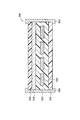
- FIG. 1A is a schematic configuration diagram of a resin material 100 according to the present embodiment.
- FIG.1 (b) is a schematic block diagram of the resin material 100 which concerns on this embodiment.
- FIG. 2 is a schematic configuration diagram of a solar cell module 500 according to the present embodiment.
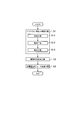
- FIG. 3 is a flowchart for explaining a method for manufacturing the resin material 100 and the solar cell module according to this embodiment.
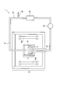
- FIG. 4 is a schematic configuration diagram of the manufacturing apparatus 1 used for manufacturing the nanosilicon fine particles 200 according to the present embodiment.
- FIG. 1A and FIG. 1B are schematic configuration diagrams of a resin material 100 according to this embodiment.
- the resin material 100 is composed of a resin 150 and nano-silicon fine particles 200. Specifically, the resin material 100 is composed of a resin 150 including the nanosilicon fine particles 200.
- thermoplastic resin for example, a thermoplastic resin, a thermosetting resin, and a resin that dissolves in a solvent are used.
- thermoplastic resin include polyethylene resins, polypropylene, EVA resins, acrylic resins, polyester resins, polyamide resins such as nylon, vinyl chloride resins, thermoplastic urethanes, polycarbonates, and fluororesins.
- thermosetting resin include thermosetting EVA resin, phenol resin, melamine resin, thermosetting urethane resin, unsaturated polyester resin, thermosetting acrylic resin, silicone resin, and epoxy resin. In addition to heat, radiation curing, electron beam curing, and ultraviolet curable resin can also be used.
- the resin that dissolves in the solvent include acrylic resin, polyester resin, urethane resin, vinyl chloride resin, polyamide resin, and polycarbonate resin.
- solvent include organic solvents and water.
- the nanosilicon fine particles 200 absorb light having a predetermined wavelength and emit light having another wavelength. Specifically, it absorbs ultraviolet rays and emits light having a wavelength in the visible region.
- the nanosilicon fine particles 200 have different emission peaks depending on the particle diameter. For this reason, the wavelength of the emitted light can be selected by using the nanosilicon fine particles 200 having a desired emission peak.
- the nano-silicon fine particles 200 are silicon fine particles having a nano-order particle size. Specifically, the nanosilicon fine particles 200 have an average particle size of 10 nm or less. The average particle size of the nanosilicon fine particles 200 is preferably 1 nm or more and 5 nm or less. In order to obtain a desired emission peak, it is preferable to change the particle diameter, and the distribution is desirably controlled to about ⁇ 0.5 nm.
- the solution is hydrophilic, it is preferable to terminate organic monomers having hydrophilic groups on the surface of the nanosilicon fine particles 200.
- the solution is hydrophobic, it is preferable to terminate an organic monomer having a hydrophobic group on the surface of the nanosilicon fine particles 200.
- the resin material 100 may be formed on a substrate 250.
- FIG. 2 is a schematic configuration diagram of a solar cell module 500 according to the present embodiment.
- the solar cell module 500 includes a power generation element 510, a sealing material 520, a transparent substrate 530, a protective film 540, a back sheet 550, and a frame 560.
- the power generation element 510 receives light and converts light energy into electric energy.
- a silicon cell is used as the power generation element 510.
- the power generation element is electrically connected to the adjacent power generation element by a wiring material.
- the sealing material 520 seals the power generation element 510.
- the sealing material 520 covers the power generation element 510 between the transparent substrate 530 and the back sheet 550 and protects the power generation element 510.
- a thermosetting resin for example, EVA is used.
- the transparent substrate 530 is disposed on the light receiving surface side of the power generation element 510.
- the transparent substrate 530 protects the surface of the solar cell module.
- a glass plate or a thermoplastic resin for example, a fluororesin or an acrylic resin is used.
- the protective film 540 is formed on the transparent substrate 530. Specifically, it is formed on the opposite surface of the transparent substrate 530 with the sealing material 520 interposed therebetween.
- the protective film 540 protects the surface of the solar cell module.
- a coating resin for example, a fluororesin or an acrylic resin
- the solar cell module 500 does not necessarily have the protective film 540.
- the back sheet 550 is disposed on the back side of the power generation element 510.
- the back sheet 550 has waterproofness and weather resistance.
- a resin sheet for example, a fluororesin or a polyester resin
- a resin sheet for example, a fluororesin or a polyester resin
- the frame 560 is used to protect the side surface of the solar cell module 500.
- the frame 560 is used for fixing a laminated structure of the protective film 540, the transparent substrate 530, the sealing material 520, and the back sheet 550 in this order.
- An aluminum frame is used as the frame 560.
- the nanosilicon fine particles 200 are included in at least one of the transparent substrate 530, the sealing material 520, and the protective film 540. All of the transparent substrate 530, the sealing material 520, and the protective film 540 may contain the nanosilicon fine particles 200.
- the nano silicon fine particles 200 absorb ultraviolet light and emit visible light. The characteristics of the nanosilicon fine particles 200 are the same as those described above.
- FIG. 2 is a schematic configuration diagram of a solar cell module 500 according to the present embodiment.
- FIG. 3 is a flowchart for explaining a method of manufacturing the resin material 100 and the solar cell module 500 according to this embodiment.
- FIG. 4 is a schematic configuration diagram of the manufacturing apparatus 1 used for manufacturing the nanosilicon fine particles 200 according to the present embodiment.
- the manufacturing method of the resin material 100 according to the present embodiment includes a nanosilicon fine particle preparation step S1 and a resin material formation step S2.
- the manufacturing method of the solar cell module 500 which concerns on this embodiment is equipped with nano silicon fine particle preparation process S1, resin material formation process S2, and solar cell module manufacturing process S3.
- Nanosilicon fine particle preparation step S1 As shown in FIG. 3, the nanosilicon fine particle preparation step S1 includes a firing step S11, a rapid cooling step S12, a removal step S13, and a replacement step S14.
- the manufacturing apparatus 1 includes a heating container 2 that contains a mixture containing a silicon source and a carbon source in a container W to form a heating atmosphere, a stage 8 that holds the heating container 2, and a container W.
- the suction device 20 can suck SiO gas while maintaining a heated and inert atmosphere in the heating container 2.
- the inside of the suction device 20 is provided so that argon gas circulates.
- an electromagnetic valve 25 that automatically opens and closes according to the set pressure is provided.
- the firing step S11 is a step of firing a mixture containing a silicon source and a carbon source in an inert atmosphere.
- Step S11 includes a step of generating a mixture from a silicon source and a carbon source (mixture generation step) and a step of baking the mixture generated in the mixture generation step (mixture baking step).
- a silicon source that is, a silicon-containing raw material
- a liquid silicon source and a solid silicon source can be used in combination.
- at least one kind must be selected from a liquid silicon source.
- alkoxysilane mono-, di-, tri-, tetra-
- tetraalkoxysilane polymers are used as the liquid silicon source.
- alkoxysilanes tetraalkoxysilane is preferably used. Specific examples include methoxysilane, ethoxysilane, propoxysilane, butoxysilane and the like. From the viewpoint of handling, ethoxysilane is preferable.
- the tetraalkoxysilane polymer include a low molecular weight polymer (oligomer) having a degree of polymerization of about 2 to 15, and a silicate polymer having a higher degree of polymerization and a liquid silicon source.
- Examples of solid silicon sources that can be used in combination with these liquid silicon sources include silicon oxide.
- Examples of silicon oxide include silica sol (a colloidal ultrafine silica-containing liquid containing OH groups and alkoxyl groups inside), silicon dioxide (silica gel, fine silica, quartz powder) and the like.
- tetraethoxysilane oligomers and mixtures of tetraethoxysilane oligomers and fine powder silica are preferred.
- the carbon source that is, the carbon-containing raw material is synthesized by using a catalyst that does not contain an impurity element, and can be any one or two or more kinds of organic materials that can be cured by being polymerized or crosslinked by heating and / or a catalyst or a crosslinking agent.
- a catalyst that does not contain an impurity element
- the carbon-containing raw material include curable resins such as phenol resins, furan resins, urea resins, epoxy resins, unsaturated polyester resins, polyimide resins, and polyurethane resins synthesized using a catalyst that does not contain an impurity element. Is mentioned.
- curable resins such as phenol resins, furan resins, urea resins, epoxy resins, unsaturated polyester resins, polyimide resins, and polyurethane resins synthesized using a catalyst that does not contain an impurity element.
- a resol type or novolac type phenol resin having a high residual carbon ratio and excellent workability is preferable.
- the resol type phenolic resin useful in the present embodiment is monovalent or 2 such as phenol, cresol, xylenol, resorcin, bisphenol A in the presence of a catalyst (specifically ammonia or organic amine) that does not contain an impurity element. It is produced by reacting a valent phenol with an aldehyde such as formaldehyde, acetaldehyde, or benzaldehyde.
- the organic amine used as the catalyst may be any of primary, secondary, and tertiary amines.
- dimethylamine, trimethylamine, diethylamine, triethylamine, dimethylmonoethanolamine, monomethyldiethanolamine, N-methylaniline, pyridine, morpholine and the like can be used.
- the novolak type phenolic resin useful in the present embodiment is a mixture of monovalent or divalent phenols and aldehydes similar to those described above, and acids containing no impurity elements (specifically, hydrochloric acid, sulfuric acid, p. -Toluenesulfonic acid or oxalic acid) can be used as a catalyst for the reaction.
- acids containing no impurity elements specifically, hydrochloric acid, sulfuric acid, p. -Toluenesulfonic acid or oxalic acid
- a conventionally well-known method can also be adopted for the production of the novolac type phenol resin. That is, 0.5 to 0.9 mole of aldehyde and 0.02 to 0.2 mole of an inorganic or organic acid not containing an impurity element are added to 1 mole of phenol and heated to 60 to 100 ° C. .
- impurities include heavy metal elements such as Fe, Ni, Cu, Cr, V, and W, alkali metal elements such as Li, Na, and K, and alkaline earth such as Be, Mg, Ca, B, Al, and Ga. Or amphoteric metal elements.
- a catalyst or a crosslinking agent for polymerization or crosslinking is added to a raw material mixture obtained by mixing a silicon-containing raw material and a carbon-containing raw material, if necessary, and dissolved in a solvent.
- a mixture is formed by causing a polymerization or crosslinking reaction.
- the raw material mixture is heated at about 150 ° C. Thereby, the mixture is dried.
- the Si / C ratio is preferably 0.5 to 3.0.
- the mixture baking step is a step of baking the mixture obtained in the mixture generation step in an inert gas atmosphere.
- the mixture is stored in a container W.
- the heating element 10a and the heating element 10b the mixture is heated and fired in an inert gas atmosphere to carbonize and silicify the mixture.
- a gas containing carbon and silicon is generated.
- silicon monoxide (SiO) is generated.
- An inert gas atmosphere is a non-oxidizing atmosphere.
- Inert gases include, for example, vacuum, nitrogen, helium or argon.
- the rapid cooling step S2 is a step of rapidly cooling a gas generated by firing the mixture to obtain a composite powder.
- the blower 23 is activated.
- the generated gas is extracted from the inside of the heating container 2 through the suction pipe 21 by being put on an argon gas stream. Since the outside of the heat insulating material 12 is kept at room temperature, the generated gas is rapidly cooled to room temperature.
- a composite powder containing silicon fine particles (Si) is obtained from the generated gas. Specifically, by cooling at a temperature of less than 1600 ° C., a composite powder containing silicon fine particles is obtained as shown by the following formula (2).
- the collected composite powder is collected in the dust collector 22.
- the argon stream is sent to the heating container 2 through the supply pipe 24.
- Removal step S13 is a step of obtaining nanosilicon fine particles 200 by removing silicon monoxide and silicon dioxide from the mixed powder.
- a heat treatment step of heating the composite powder obtained in the rapid cooling step S12 in an inert atmosphere may be performed.
- the crystallinity of the nanosilicon fine particles 200 can be improved.
- a rare gas is used to make the inert atmosphere.
- the heat treatment process is performed in a temperature range of 800 ° C. to 1300 ° C.
- the heat treatment step is preferably performed in a temperature range of 900 ° C. to 1100 ° C.
- a step of heating the composite powder in an acidic atmosphere may be performed.
- the surface of the silicon fine particles contained in the composite powder is oxidized. Specifically, silicon forming the surface of the silicon fine particles is oxidized into silicon dioxide.
- the surface of the silicon fine particles having a larger particle diameter is oxidized compared to the silicon fine particles having a smaller particle diameter. Therefore, the silicon particles having a small particle size do not become so small as compared with the ratio in which the particle size of the silicon particles having a large particle size is reduced by oxidation. Therefore, nanosilicon fine particles 200 having a uniform particle diameter can be obtained.
- the same effect as the heat treatment step of heating in an inert atmosphere can be obtained, and thus the heat treatment step in an inert atmosphere may be omitted.
- the particle size of the nano silicon fine particles can be controlled. Specifically, the higher the heating temperature, the more the surface of the silicon fine particles is oxidized to silicon dioxide. Therefore, the higher the heating temperature, the smaller the average particle size of the resulting nanosilicon fine particles.
- the composite powder in which the surface of the silicon fine particles is oxidized into silicon dioxide by the heating process may be crushed.
- a ball mill is used for crushing. By crushing, the composite powder is finely crushed.
- the pulverized composite powder is separated by centrifugation. Thereby, the composite powder containing the silicon fine particles 200 with uniform particle diameter can be obtained.
- the resin material forming step S2 may be performed using the composite powder.
- the composite powder obtained by the rapid cooling step S12, the heating step, or the crushing / centrifugation step is immersed in an etching solution containing at least hydrofluoric acid for etching.
- the mixed powder is immersed in an etching solution containing hydrofluoric acid and an oxidizing agent for etching.
- the emission peak tends to shift to the short wavelength side.
- the nanosilicon fine particles 200 having a desired light emission peak are obtained by taking out the nanosilicon fine particles 200 from the etching solution when the etching has progressed to such an extent that a desired light emission peak is obtained, and drying appropriately.
- the etching solution may be mixed with a hydrophobic solvent (for example, cyclohexane) and a slightly polar solvent (for example, 2-propanol).
- a hydrophobic solvent for example, cyclohexane
- a slightly polar solvent for example, 2-propanol
- the oxidizing agent and hydrofluoric acid are contained.
- the nano silicon fine particles 200 may be obtained by an etching process immersed in a solution.
- the amount of hydrofluoric acid or the concentration of hydrofluoric acid is adjusted according to the amount of the composite powder.
- the composite powder is an equimolar mixture of silicon monoxide and silicon dioxide. That is, when the number of moles of the composite powder to be immersed is 2x, it is assumed that the composite powder contains x moles of SiO and SiO 2 , respectively.
- the minimum amount of hydrofluoric acid required to dissolve all equimolar mixtures is equivalent. This minimum necessary hydrofluoric acid can be calculated using the following equations (3) and (4).
- hydrofluoric acid it is preferable to add hydrofluoric acid to the solvent to which the mixed powder has been added over time. Specifically, it is preferable to add hydrofluoric acid to the solvent at a rate of 1 ml or less per minute. A rapid exotherm can be suppressed by slowly adding hydrofluoric acid to the solvent over time. Moreover, foaming can also be suppressed.
- the composite powder It is preferable to immerse the composite powder in an etching solution containing hydrofluoric acid for 1 hour or longer. More preferably, the composite powder is immersed in an etching solution containing hydrofluoric acid for 48 hours or more. After 48 hours, since the reaction between hydrofluoric acid and the composite powder has converged, silicon monoxide and silicon dioxide including the silicon surface can be more reliably removed.
- the nanosilicon fine particles 200 can be obtained by immersing the thus obtained mixed powder from which silicon monoxide and silicon dioxide have been removed in a solution containing an oxidizing agent and hydrofluoric acid.
- the composite powder immersed in the etching solution may be irradiated with light having energy larger than the band gap energy of silicon contained in the composite powder.
- the band gap energy of silicon contained in the composite powder varies depending on the particle size of silicon (silicon fine particles). Therefore, in order to obtain the nano silicon fine particles 200 having a desired particle size, the irradiation light and the etching time are appropriately adjusted.
- the monochromatic light which is light which consists only of a fixed wavelength is preferable for the light to irradiate. This is because it is easier to control the particle diameter than light having a plurality of wavelengths.
- Etching is performed while irradiating light, and when the nano silicon fine particles 200 having a desired particle diameter are obtained, the nano silicon fine particles 200 are taken out from the etching solution. The extracted nanosilicon fine particles 200 are appropriately dried. Thereby, the nano silicon fine particles 200 are obtained.
- the nanosilicon fine particles 200 do not have to be completely removed of silicon monoxide and silicon dioxide. If there is no obstacle to wavelength conversion, the silicon monoxide and silicon dioxide are partially or entirely covered. The nano silicon fine particles 200 may be included.
- H atoms are partially added to the surface of the nano-silicon fine particles 200 subjected to the etching process by hydrofluoric acid used in the etching process. Therefore, an unsaturated hydrocarbon group having a hydrophilic group may be introduced on the surface of the nanosilicon fine particle 200. That is, the H atom added to the surface of the nanosilicon fine particle 200 may be substituted with an unsaturated hydrocarbon group having a hydrophilic group.
- the H atom of Si—H which is the active terminal of the nanosilicon fine particle 200, is replaced with an unsaturated hydrocarbon group having a hydrophilic group.
- An unsaturated hydrocarbon group having a hydrophilic group is a group generated from an isoprenoid compound having a hydrophilic group.
- monoterpenoids such as linalool are applicable.
- the unsaturated hydrocarbon group having a hydrophilic group may be a group generated from an allyl compound having a hydrophilic group.
- allyl alcohol, eugenol, etc. are applicable.
- the unsaturated hydrocarbon group having a hydrophilic group is preferably a naturally-derived polymer that is non-toxic to living bodies.
- a group generated from an isoprenoid compound having a hydrophobic group can be introduced on the surface of the nanosilicon fine particle 200.
- monoterpenoids such as ⁇ pinene are applicable.
- Dispersibility in organic solvents is improved by substituting the H atom of Si-H, which is the active terminal of the nanosilicon fine particle 200, with an unsaturated hydrocarbon group generated from a monoterpenoid having a hydrophobic group such as ⁇ -pinene. can do.
- the resin material forming step S2 is performed using the nanosilicon fine particles 200 thus prepared.
- the prepared nano silicon fine particles 200 have a particle diameter that absorbs ultraviolet light and emits visible light.
- the resin material forming step S2 is a step in which the prepared nanosilicon fine particles 200 are contained in the resin 150.
- the resin 150 examples include thermoplastic resins (for example, acrylic resins) and thermosetting resins (for example, thermosetting EVA resins).
- the nano silicon fine particles 200 are added to the resin 150 and mixed.
- the resin 150 mixed with the nano silicon fine particles 200 is pelletized.
- the resin material 100 having an arbitrary shape is manufactured from the pelletized resin 150 by calendaring, extrusion molding, injection molding, or the like.
- a film-like resin material 100 may be manufactured.
- the resin 150 has thermosetting properties, it may be cross-linked by heat, light, electron beam, radiation, or the like.
- the resin 150 and the nanosilicon fine particles 200 may be added to the soluble solvent.
- the resin material 100 having an arbitrary shape may be manufactured by using a solution in which the resin 150 is dissolved, for example, using a coating method or a printing method. A film-like resin material 100 may be manufactured. As shown in FIG. 1B, the resin material 100 may be formed on the substrate 250.
- the resin 150 has thermosetting properties, it may be cross-linked by heat, light, electron beam, radiation or the like.
- the resin material 100 composed of the resin 150 including the nano-silicon fine particles 200 that absorb light of a predetermined wavelength and emit light of another wavelength can be manufactured.
- the nanosilicon fine particles 200 may be added to the resin 150 suitable for each member of the solar cell module (for example, the transparent substrate 530, the sealing material 520, and the protective film 540).
- the resin material 100 including the nanosilicon fine particles 200 may be added to the thermoplastic resin.
- the nanosilicon fine particles 200 may be added to the thermosetting resin.
- the nanosilicon fine particles 200 may be added to a solution in which the resin 150 is dissolved.
- the solar cell module manufacturing step S3 is a step of manufacturing a solar cell module using a resin containing nano-silicon fine particles.
- a plurality of power generation elements 510 that are electrically connected to each other are prepared.
- the resin material containing nano-silicon fine particles is used in at least one of the transparent substrate 530, the sealing material 520, and the protective film 540.
- a resin containing nano-silicon fine particles is used as a sealing material 520 for sealing the power generation element 510. It is provided on the light receiving surface side of the power generation element 510 and used as a transparent substrate 530 that transmits light.
- a sealing material 520 On the transparent substrate 530, a sealing material 520, a plurality of power generation elements 510, a sealing material 520, and a back sheet 550 are sequentially stacked to form a stacked body. This laminate is heated under predetermined conditions. A protective film 540 is formed on the transparent substrate 530. Thereafter, the frame 560 is attached.
- the solar cell module 500 according to this embodiment is formed.
- the nanosilicon fine particles 200 are prepared as the wavelength conversion material in the nanosilicon fine particle preparation step S1. That is, the nano silicon fine particles 200 are used as the wavelength conversion material.
- the nanosilicon fine particles 200 have different emission peaks depending on the particle diameter. Therefore, by adjusting the particle size of the nanosilicon fine particles 200 contained in the resin 150, the resin material according to the present invention can have a different wavelength of emitted light than the existing resin material. That is, the resin material 100 can select the wavelength of the emitted light as compared with the conventional resin material.
- the nanosilicon fine particle preparation step S1 includes a firing step S11, a rapid cooling step S12, and a removal step S13. Further, in the nanosilicon fine particle preparing step S1, the mixed powder is immersed in an etching solution containing at least hydrofluoric acid for etching. The etching solution contains an oxidant. Thereby, the silicon fine particles contained in the mixed powder are etched, and the nano silicon fine particles 200 are obtained.
- the mixed powder in the nanosilicon fine particle preparation step S1, is immersed in an etching solution that does not contain an oxidant and contains hydrofluoric acid, and the silicon monoxide and the dioxide dioxide from the mixed powder Part of silicon is removed, and the mixed powder from which part of silicon monoxide and silicon dioxide has been removed is immersed in a solution containing an oxidizing agent and hydrofluoric acid.
- an etching solution that does not contain an oxidizing agent and contains hydrofluoric acid By immersing the mixed powder in an etching solution that does not contain an oxidizing agent and contains hydrofluoric acid, the silicon fine particles contained in the mixed powder are not removed, but only the silicon monoxide and silicon dioxide contained in the mixed powder are removed. Is done.
- the particle size of the silicon particles remains unchanged. For this reason, a mixed powder containing silicon fine particles whose particle diameter does not change and silicon monoxide and silicon dioxide from which a part has been removed is obtained.
- This mixed powder can reduce the time for removing silicon monoxide and silicon dioxide by the amount of silicon monoxide and silicon dioxide removed, compared to the mixed powder obtained by the rapid cooling step S12. Therefore, the time available for adjusting the particle size of the silicon fine particles increases. Furthermore, since the amount of silicon fine particles covered with silicon monoxide and silicon dioxide is reduced, the particle size can be controlled more easily than when the silicon fine particles are covered with silicon monoxide and silicon dioxide thickly. Therefore, since the nanosilicon fine particles 200 having a desired emission peak are obtained, the resin material 100 capable of selecting the wavelength of emitted light can be manufactured.
- the composite powder immersed in the etching solution is irradiated with light having energy larger than the band gap energy of the silicon fine particles. good.
- the silicon fine particles are irradiated with light having energy larger than the band gap energy, electron-hole pairs are generated inside the silicon fine particles, and the reaction between the silicon fine particles and hydrofluoric acid is promoted.
- etching of silicon fine particles is promoted.
- the silicon fine particles have a larger band gap energy as the particle size is smaller. For this reason, since silicon fine particles having a band gap energy larger than the irradiated energy do not generate electron-hole pairs, the promotion of etching can be suppressed.
- the silicon fine particles having a large particle size are etched quickly because the etching is promoted. Etching is performed slowly when the particle size of the band gap energy is larger than the irradiated energy. As a result, since the particle size distribution of the obtained nanosilicon fine particles 200 becomes sharp, the nanosilicon fine particles 200 having a uniform particle size can be obtained.
- the method further includes the step of replacing the hydrogen atom added to the surface of the nanosilicon fine particle 200 obtained by etching with an organic monomer having a hydrophilic group or a hydrophobic group. .
- the nanosilicon fine particles 200 can be prevented from aggregating in the solution.
- the soluble resin 150 is easily distributed evenly.
- the method further includes the step of heating the composite powder in an oxidizing atmosphere, and in the step of obtaining nanosilicon fine particles from the composite powder, the nanoparticle is heated from the heated composite powder.
- Silicon fine particles 200 are obtained.
- the surface of the silicon fine particles contained in the composite powder is oxidized, and silicon dioxide is formed.
- Silicon dioxide is harder to form as the silicon particles have a smaller particle size. For this reason, the surface of the silicon fine particles having a large particle size is more oxidized to silicon dioxide, and the surface of the silicon fine particles having a small particle size is hardly oxidized to silicon dioxide. Therefore, since nanosilicon fine particles having a uniform particle diameter can be obtained, the wavelength of emitted light can be selected more.
- the step S1 of preparing the nanosilicon fine particles 200 that absorb ultraviolet light and emit visible light and the step S2 of containing the nanosilicon fine particles 200 in the resin 150
- a step S3 of manufacturing a solar cell module using the resin material 100 is manufactured using resin 150 containing nano-silicon fine particles 200 that absorb ultraviolet light and emit visible light.
- a solar cell module having a plurality of power generation elements is known (for example, JP 2010-109090 A).
- the solar cell module has a sealing material for sealing the power generation element and a transparent substrate. This protects the power generating element and facilitates the handling of the solar cell module.
- Sunlight has light in a wide wavelength region including ultraviolet light and visible light. However, even if sunlight is incident on the power generation element, light energy cannot be converted into electric energy for light in all wavelength regions. The light in the wavelength region absorbed by the power generation element is determined by the physical properties of the power generation element. In a general power generation element, visible light is absorbed and converted into electric energy, but ultraviolet light has not been sufficiently utilized. Therefore, it has been demanded to improve power generation efficiency by effectively using light in a wider wavelength region.
- Nanoparticles 200 absorb ultraviolet light and emit visible light. For this reason, since the power generation element 510 absorbs visible light radiated from the nanosilicon fine particles 200, ultraviolet light that was not originally absorbed is used, so that power generation efficiency is improved.
- the nanosilicon fine particles 200 have a nano-order particle size, even if they are contained in the resin 150, they do not interfere with light. Therefore, even if the resin 150 includes the nanosilicon fine particles 200, the power generation efficiency does not decrease.
- the nanosilicon fine particles 200 have different emission peaks depending on the particle diameter. For this reason, the wavelength of the emitted light can also be adjusted by adjusting the particle diameter of the nanosilicon fine particles 200 contained in the resin 150. Thereby, since the wavelength of the emitted light can be adjusted according to the light absorption characteristics of the power generation element 510, the power generation efficiency is improved.
- Example 1 The solar cell modules of Example 1 and Comparative Example 1 were each generated and the power generation efficiency was compared. As a result, it was found that the power generation efficiency was improved in Example 1 compared to Comparative Example 1.
- Nanosilicon fine particles were added to the heat resistant acrylic resin to form a resin plate.
- a solar cell module was manufactured using this resin plate as the transparent substrate 530 (Example 2).
- a solar cell module was manufactured using a heat-resistant acrylic resin containing no nanosilicon fine particles as the transparent substrate 530 (Comparative Example 2).
- Example 2 The solar cell modules of Example 2 and Comparative Example 2 were each generated and the power generation efficiency was compared. As a result, it was found that the power generation efficiency was improved in Example 2 compared to Comparative Example 2.
- Nanosilicon fine particles were added to thermosetting EVA.
- a solar cell module was manufactured using EVA added with nano-silicon fine particles as the sealing material 520 (Example 3).
- a solar cell module was manufactured using thermosetting EVA containing no nano-silicon fine particles as the sealing material 520 (Comparative Example 3).
- Example 3 The solar cell modules of Example 3 and Comparative Example 3 were each generated to compare the power generation efficiency. As a result, it was found that the power generation efficiency was improved in Example 3 compared to Comparative Example 3.
- the present invention it is possible to provide a resin material that allows more selection of the wavelength of emitted light. Moreover, according to this invention, the solar cell module which improved the electric power generation efficiency effectively using an ultraviolet light can be provided.
Landscapes
- Chemical & Material Sciences (AREA)
- Organic Chemistry (AREA)
- Engineering & Computer Science (AREA)
- Inorganic Chemistry (AREA)
- Nanotechnology (AREA)
- Chemical Kinetics & Catalysis (AREA)
- Polymers & Plastics (AREA)
- Physics & Mathematics (AREA)
- Medicinal Chemistry (AREA)
- Composite Materials (AREA)
- Condensed Matter Physics & Semiconductors (AREA)
- General Physics & Mathematics (AREA)
- Materials Engineering (AREA)
- Crystallography & Structural Chemistry (AREA)
- Health & Medical Sciences (AREA)
- Silicon Compounds (AREA)
Abstract
本発明は、所定の波長の光を吸収して、別の波長の光を放射する波長変換材料を準備する工程S1と、準備した波長変換材料を樹脂に含有する工程S2と、を備える樹脂材料の製造方法であって、波長変換材料を準備する工程S2では、波長変換材料としてナノシリコン微粒子200を準備する。
Description
本発明は、所定の波長の光を吸収して、別の波長の光を放射する波長変換材料が含まれた樹脂によって構成される樹脂材料の製造方法及び樹脂材料に関する。また、本発明は、その樹脂材料を利用した太陽電池モジュールの製造方法及び太陽電池モジュールに関する。
従来、所定の波長の光を吸収して、別の波長の光を放射する波長変換材料が含まれた樹脂によって構成される樹脂材料がある。このような樹脂材料は、発光性樹脂パネルや蛍光膜形成材料として用いられる。波長変換材料として、希土類金属錯体(例えば、特許文献1参照)や蛍光色素(例えば、特許文献2参照)が用いられている。
しかしながら、希土類金属錯体は、分子構造及び配位金属種によって蛍光発光波長が決まるため、放出される光の波長が限られていた。蛍光色素についても同様であった。このため、放出される光の波長をより選択可能な新たな樹脂材料が求められていた。
そこで、本発明は、このような状況に鑑みてなされたものであり、放出される光の波長をより選択可能な新たな樹脂材料の製造方法及び樹脂材料、その樹脂材料を用いた太陽電池モジュールの製造方法及び太陽電池モジュールを提供することを目的とする。
上述した課題を解決するため、本発明は、次のような特徴を有している。本発明の特徴は、所定の波長の光を吸収して、別の波長の光を放射する波長変換材料を準備する工程と、準備した前記波長変換材料を樹脂に含有する工程と、を備える樹脂材料の製造方法であって、前記波長変換材料を準備する工程では、前記波長変換材料としてナノシリコン微粒子を準備することを要旨とする。
本発明の特徴によれば、波長変換材料を準備する工程では、波長変換材料としてナノシリコン微粒子を準備する。ナノシリコン微粒子は、粒径によって発光ピークが異なる。このため、樹脂に含まれるナノシリコン微粒子の粒径を調整することにより、本発明に係る樹脂材料は、既存の樹脂材料よりも、放出される光の波長を異ならせることができる。すなわち、本発明に係る樹脂材料は、放出される光の波長が従来の樹脂材料よりも選択できる。なお、ナノシリコン微粒子とは、ナノオーダーの粒径を有するシリコン微粒子である。
前記波長変換材料を準備する工程は、不活性雰囲気下において、ケイ素源と炭素源とを含む混合物を焼成する焼成工程と、混合物を焼成することにより生成した気体を急冷し、シリコン微粒子を含む複合粉体を得る急冷工程と、前記複合粉体からナノシリコン微粒子を得る工程と、を備えてもよい。
前記複合粉体からナノシリコン微粒子を得る工程では、少なくともフッ酸を含むエッチング溶液に前記混合粉体を浸漬して、前記混合粉体をエッチングする工程を備えていてもよい。
前記エッチング溶液は、酸化剤を含んでもよい。
前記複合粉体からナノシリコン微粒子を得る工程では、酸化剤を含まない前記エッチング溶液に前記混合粉体を浸漬し、前記混合粉体から一酸化ケイ素及び二酸化ケイ素の一部を除去し、一酸化ケイ素及び二酸化ケイ素の一部が除去された混合粉体を酸化剤及びフッ酸を含む溶液に浸漬してもよい。
前記複合粉体からナノシリコン微粒子を得る工程では、前記シリコン微粒子のバンドギャップエネルギーよりも大きいエネルギーを有する光を、前記エッチング溶液に浸漬した前記複合粉体に照射してもよい。
前記複合粉体からナノシリコン微粒子を得る工程は、エッチングされて得られたナノシリコン微粒子の表面に付加された水素原子を、親水基又は疎水基を有する有機モノマー基によって置換する工程をさらに備えてもよい。
前記複合粉体からナノシリコン微粒子を得る工程は、酸化雰囲気下において、前記複合粉体を加熱する工程をさらに備え、前記複合粉体からナノシリコン微粒子を得る工程において、加熱された複合粉体からナノシリコン微粒子を得てもよい。
前記波長変換材料を樹脂に含有する工程では、熱可塑性を有する樹脂に前記ナノシリコン微粒子を含有してもよい。
前記波長変換材料を樹脂に含有する工程では、熱硬化性を有する樹脂に前記ナノシリコン微粒子を含有してもよい。
前記波長変換材料を樹脂に含有する工程では、溶媒に溶解可能な前記樹脂と前記ナノシリコン微粒子とを前記溶媒に添加してもよい。
本発明の他の特徴は、上述したいずれかの製造方法を用いて製造された樹脂材料であることを要旨とする。
本発明の他の特徴は、紫外光を吸収して、可視光を放射するナノシリコン微粒子を準備する工程と、前記ナノシリコン微粒子を樹脂に含有する工程と、前記樹脂を用いて太陽電池モジュールを製造する工程と、を備えたことを要旨とする。
前記ナノシリコン微粒子を準備する工程は、不活性雰囲気下において、ケイ素源と炭素源とを含む混合物を焼成する焼成工程と、混合物を焼成することにより生成した気体を急冷し、シリコン微粒子を含む複合粉体を得る急冷工程と、前記複合粉体からナノシリコン微粒子を得る工程と、を備えてもよい。
前記複合粉体からナノシリコン微粒子を得る工程では、少なくともフッ酸を含むエッチング溶液に前記混合粉体を浸漬して、前記混合粉体をエッチングする工程を備えることを要旨とする。
前記エッチング溶液は、酸化剤を含んでもよい。
前記複合粉体からナノシリコン微粒子を得る工程では、酸化剤を含まない前記エッチング溶液に前記混合粉体を浸漬し、前記混合粉体から一酸化ケイ素及び二酸化ケイ素の一部を除去し、一酸化ケイ素及び二酸化ケイ素の一部が除去された混合粉体を酸化剤及びフッ酸を含む溶液に浸漬してもよい。
前記複合粉体からナノシリコン微粒子を得る工程では、前記シリコン微粒子のバンドギャップエネルギーよりも大きいエネルギーを有する光を、前記エッチング溶液に浸漬した前記複合粉体に照射してもよい。
前記複合粉体からナノシリコン微粒子を得る工程は、エッチングされて得られたナノシリコン微粒子の表面に付加された水素原子を、親水基又は疎水基を有する有機モノマー基によって置換する工程をさらに備えてもよい。
前記複合粉体からナノシリコン微粒子を得る工程は、酸化雰囲気下において、前記複合粉体を加熱する工程をさらに備え、前記複合粉体からナノシリコン微粒子を得る工程において、加熱された複合粉体からナノシリコン微粒子を得てもよい。
前記樹脂を用いて太陽電池モジュールを製造する工程では、発電素子をする封止する封止材として、前記樹脂を用いてもよい。
前記樹脂を用いて太陽電池モジュールを製造する工程では、発電素子の受光面側に設けられ、光を透過する透明基板として、前記樹脂を用いてもよい。
前記樹脂を用いて太陽電池モジュールを製造する工程では、発電素子の受光面側に設けられ、光を透過する透明基板上に形成される保護膜として、前記樹脂を用いてもよい。
本発明の他の特徴は、上述したいずれかの製造方法を用いて製造された太陽電池モジュールであることを要旨とする。
本発明に係る樹脂材料及び太陽電池モジュールの一例について、図面を参照しながら説明する。具体的には、(1)樹脂材料100の概略構成、(2)太陽電池モジュール500の概略構成、(3)樹脂材料100及び太陽電池モジュールの製造方法、(4)作用効果、(5)比較評価、について説明する。
以下の図面の記載において、同一または類似の部分には、同一又は類似の符号を付している。図面は模式的なのものであり、各寸法の比率などは現実のものとは異なることを留意すべきである。従って、具体的な寸法などは以下の説明を参酌して判断すべきものである。図面相互間においても互いの寸法の関係や比率が異なる部分が含まれていることは勿論である。
(1)樹脂材料100の概略構成
本実施形態に係る樹脂材料100の概略構成について、図1を参照しながら説明する。図1(a)及び図1(b)は、本実施形態に係る樹脂材料100の概略構成図である。
本実施形態に係る樹脂材料100の概略構成について、図1を参照しながら説明する。図1(a)及び図1(b)は、本実施形態に係る樹脂材料100の概略構成図である。
図1(a)に示されるように、樹脂材料100は、樹脂150とナノシリコン微粒子200とによって構成される。具体的には、樹脂材料100は、ナノシリコン微粒子200が含まれた樹脂150によって構成される。
樹脂150には、例えば、熱可塑性を有する樹脂、熱硬化性を有する樹脂及び溶媒に溶解する樹脂が用いられる。熱可塑性を有する樹脂としては、例えば、ポリエチレン、ポリプロピレン、EVA樹脂、アクリル樹脂、ポリエステル樹脂、ナイロン等のポリアミド樹脂、塩ビ樹脂、熱可塑ウレタン、ポリカーボネート、フッ素樹脂が挙げられる。熱硬化性を有する樹脂としては、例えば、熱硬化型EVA樹脂、フェノール樹脂、メラミン樹脂、熱硬化ウレタン樹脂、不飽和ポリエステル樹脂、熱硬化アクリル樹脂、シリコン樹脂、エポキシ樹脂が挙げられる。熱以外にも、放射線硬化、電子線硬化、紫外線硬化樹脂も用いることができる。溶媒に溶解する樹脂としては、例えば、アクリル樹脂、ポリエステル樹脂、ウレタン樹脂、塩ビ樹脂、ポリアミド樹脂、ポリカーボネート樹脂が挙げられる。溶媒としては、有機溶剤や水が挙げられる。
ナノシリコン微粒子200は、所定の波長の光を吸収して、別の波長の光を放射する。具体的には、紫外線を吸収して可視領域における波長の光を放射する。ナノシリコン微粒子200は、粒径によって発光ピークが異なる。このため、所望の発光ピークを有するナノシリコン微粒子200を用いることにより、放出される光の波長が選択可能となる。
ナノシリコン微粒子200は、ナノオーダーの粒径を有するシリコン微粒子である。具体的には、ナノシリコン微粒子200は、平均粒径が10nm以下である。ナノシリコン微粒子200の平均粒径は、1nm以上、5nm以下が好ましい。所望の発光ピークを得るために、粒径を変えることが好ましく、その分布は±0.5nm程度に制御することが望ましい。
ナノシリコン微粒子200の表面には、有機分子を終端させることが望ましく、溶液が親水性の場合、ナノシリコン微粒子200の表面に親水基を有する有機モノマーを終端させることが好ましい。溶液が疎水性の場合、ナノシリコン微粒子200の表面に疎水基を有する有機モノマーを終端することが好ましい。これにより、ナノシリコン微粒子200は、溶液中で凝集することを防ぐことができる。その結果、可溶性樹脂150において、均等に分布しやすくなる。
図1(b)に示されるように、樹脂材料100は、基板250上に形成されても良い。
(2)太陽電池モジュール500の概略構成
本実施形態に係る樹脂材料の概略構成について、図2を参照しながら説明する。図2は、本実施形態に係る太陽電池モジュール500の概略構成図である。
本実施形態に係る樹脂材料の概略構成について、図2を参照しながら説明する。図2は、本実施形態に係る太陽電池モジュール500の概略構成図である。
図2に示されるように、太陽電池モジュール500は、発電素子510、封止材520、透明基板530、保護膜540、裏面シート550、フレーム560を有する。
発電素子510は、光を受光し、光エネルギーを電気エネルギーへと変換する。発電素子510として、例えば、シリコンセルが用いられる。図示されていないが、発電素子は、配線材によって、隣接する発電素子と電気的に接続されている。
封止材520は、発電素子510を封止する。封止材520は、透明基板530と裏面シート550との間で発電素子510を覆っており、発電素子510を保護する。封止材としては、例えば、熱硬化性樹脂(例えば、EVA)が用いられる。
透明基板530は、発電素子510の受光面側に配置される。透明基板530は、太陽電池モジュールの表面を保護する。透明基板530としては、例えば、ガラス板、熱可塑性樹脂(例えば、フッ素樹脂、アクリル樹脂)が用いられる。
保護膜540は、透明基板530上に形成される。具体的には、封止材520を挟んで透明基板530の反対側の面に形成される。保護膜540は、太陽電池モジュールの表面を保護する。保護膜540としては、例えば、塗工性の樹脂(例えば、フッ素樹脂、アクリル系樹脂)が用いられる。なお、太陽電池モジュール500は、保護膜540を必ずしも有していなくても良い。
裏面シート550は、発電素子510の裏面側に配置される。裏面シート550は、防水性及び耐候性を有する。裏面シート550としては、例えば、樹脂シート(例えば、フッ素樹脂、ポリエステル樹脂)が用いられる。
フレーム560は、太陽電池モジュール500の側面を保護するために用いられる。また、フレーム560は、保護膜540、透明基板530、封止材520、裏面シート550の順に積層されたものを固定するために用いられる。フレーム560としては、アルミフレームが用いられる。
本実施形態に係る太陽電池モジュール500において、透明基板530、封止材520、保護膜540の少なくともいずれかに、ナノシリコン微粒子200が含まれる。透明基板530、封止材520、保護膜540の全てにおいて、ナノシリコン微粒子200を含んでいても良い。ナノシリコン微粒子200は、紫外光を吸収して、可視光を放射する。ナノシリコン微粒子200の特徴は、上述した特徴と同様である。
(3)樹脂材料100及び太陽電池モジュール500の製造方法
本実施形態に係る樹脂材料100及び太陽電池モジュール500の製造方法について、図2から図4を参照しながら説明する。図2は、本実施形態に係る太陽電池モジュール500の概略構成図である。図3は、本実施形態に係る樹脂材料100及び太陽電池モジュール500の製造方法を説明するためのフローチャートである。図4は、本実施形態に係るナノシリコン微粒子200の製造に用いられる製造装置1の概略構成図である。図2に示されるように、本実施形態に係る樹脂材料100の製造方法は、ナノシリコン微粒子準備工程S1と樹脂材料形成工程S2とを備える。また、本実施形態に係る太陽電池モジュール500の製造方法は、ナノシリコン微粒子準備工程S1と樹脂材料形成工程S2と太陽電池モジュール製造工程S3とを備える。
本実施形態に係る樹脂材料100及び太陽電池モジュール500の製造方法について、図2から図4を参照しながら説明する。図2は、本実施形態に係る太陽電池モジュール500の概略構成図である。図3は、本実施形態に係る樹脂材料100及び太陽電池モジュール500の製造方法を説明するためのフローチャートである。図4は、本実施形態に係るナノシリコン微粒子200の製造に用いられる製造装置1の概略構成図である。図2に示されるように、本実施形態に係る樹脂材料100の製造方法は、ナノシリコン微粒子準備工程S1と樹脂材料形成工程S2とを備える。また、本実施形態に係る太陽電池モジュール500の製造方法は、ナノシリコン微粒子準備工程S1と樹脂材料形成工程S2と太陽電池モジュール製造工程S3とを備える。
(3.1)ナノシリコン微粒子準備工程S1
図3に示されるように、ナノシリコン微粒子準備工程S1は、焼成工程S11、急冷工程S12、除去工程S13及び置換工程S14を有する。
図3に示されるように、ナノシリコン微粒子準備工程S1は、焼成工程S11、急冷工程S12、除去工程S13及び置換工程S14を有する。
図4に示されるように、製造装置1は、珪素源と炭素源を含む混合物を容器Wに収容し加熱雰囲気を形成する加熱容器2と、加熱容器2を保持するステージ8と、容器Wに収容された混合物を加熱する発熱体10a及び発熱体10bと、加熱容器2と発熱体10a及び発熱体10bを覆う断熱材12と、加熱容器2から吸引管21を介して反応ガスを吸引するブロア23と、複合粉体を収容する集塵機22と、ガスを供給する供給管24を有する吸引装置20と、を備える。吸引装置20は加熱容器2内に加熱及び不活性雰囲気を維持しながらSiOガスを吸引することができる。吸引装置20内は、アルゴンガスが循環するように設けられている。また設定圧力により自動開閉する電磁弁25を備える。
(3.1.1)焼成工程S11
焼成工程S11は、不活性雰囲気下において、珪素源と炭素源とを含む混合物を焼成する工程である。工程S11は、珪素源と炭素源とから混合物を生成する工程(混合物生成工程)と、混合物生成工程で生成された混合物を焼成する工程(混合物焼成工程)とを有する。
焼成工程S11は、不活性雰囲気下において、珪素源と炭素源とを含む混合物を焼成する工程である。工程S11は、珪素源と炭素源とから混合物を生成する工程(混合物生成工程)と、混合物生成工程で生成された混合物を焼成する工程(混合物焼成工程)とを有する。
珪素源、すなわち、珪素含有原料としては、液状の珪素源と固体状の珪素源とを併用することができる。ただし、少なくとも一種は、液状の珪素源から選ばれなくてはならない。
液状の珪素源としては、アルコキシシラン(モノ-、ジ-、トリ-、テトラ-)及びテトラアルコキシシランの重合体が用いられる。アルコキシシランの中ではテトラアルコキシシランが好適に用いられる。具体的には、メトキシシラン、エトキシシラン、プロポキシシラン、ブトキシシラン等が挙げられる。ハンドリングの点からは、エトキシシランが好ましい。テトラアルコキシシランの重合体としては、重合度が2~15程度の低分子量重合体(オリゴマー)及びさらに重合度が高いケイ酸ポリマーで液状の珪素源が挙げられる。
これら液状の珪素源と併用可能な固体状の珪素源としては、酸化珪素が挙げられる。酸化珪素には、SiOの他、シリカゾル(コロイド状超微細シリカ含有液、内部にOH基やアルコキシル基を含む)、二酸化珪素(シリカゲル、微細シリカ、石英粉体)等が挙げられる。
これら珪素源のなかでも、均質性やハンドリング性の観点から、テトラエトキシシランのオリゴマー及びテトラエトキシシランのオリゴマーと微粉体シリカとの混合物等が好適である。
炭素源、すなわち、炭素含有原料は、不純物元素を含まない触媒を用いて合成され、加熱及び/又は触媒、若しくは架橋剤により重合又は架橋して硬化しうる任意の1種もしくは2種以上の有機化合物から構成されるモノマー、オリゴマー及びポリマーである。
炭素含有原料の好適な具体例としては、不純物元素を含まない触媒を用いて合成されたフェノール樹脂、フラン樹脂、尿素樹脂、エポキシ樹脂、不飽和ポリエステル樹脂、ポリイミド樹脂、ポリウレタン樹脂などの硬化性樹脂が挙げられる。特に、残炭率が高く、作業性に優れているレゾール型またはノボラック型フェノール樹脂が好ましい。
本実施形態に有用なレゾール型フェノール樹脂は、不純物元素を含まない触媒(具体的には、アンモニアまたは有機アミン)の存在下において、フェノール、クレゾール、キシレノール、レゾルシン、ビスフェノールAなどの1価または2価のフェノール類と、ホルムアルデヒド、アセトアルデヒド、ベンズアルデヒド等のアルデヒド類とを反応させて製造する。
触媒として用いる有機アミンは、第一級、第二級、および第三級アミンのいずれでもよい。有機アミンとしては、ジメチルアミン、トリメチルアミン、ジエチルアミン、トリエチルアミン、ジメチルモノエタノールアミン、モノメチルジエタノールアミン、N-メチルアニリン、ピリジン、モルホリン等を用いることができる。
フェノール類とアルデヒド類とをアンモニアまたは有機アミンの存在下に反応させてレゾール型フェノール樹脂を合成する方法は、使用触媒が異なる以外は、従来公知の方法を採用できる。
即ち、フェノール類1モルに対し、1~3モルのアルデヒド類と0.02~0.2モルの有機アミン又はアンモニアを加え、60~100℃に加熱する。
一方、本実施形態に有用なノボラック型フェノール樹脂は、上記と同様の1価または2価フェノール類とアルデヒド類とを混合し、不純物元素を含まない酸類(具体的には、塩酸、硫酸、p-トルエンスルホン酸またはシュウ酸など)を触媒として反応させて製造することができる。
ノボラック型フェノール樹脂の製造も従来公知の方法を採用できる。即ち、フェノール類1モルに対し、0.5~0.9モルのアルデヒド類と0.02~0.2モルの不純物元素を含まない無機酸又は有機酸を加え、60~100℃に加熱する。
なお、不純物の一例として、Fe、Ni、Cu、Cr、V、W等の重金属元素、Li、Na、K等のアルカリ金属元素、並びにBe、Mg、Ca、B、Al、Ga等のアルカリ土類若しくは両性金属元素などが挙げられる。
混合物生成工程では、珪素含有原料と炭素含有原料とを混合した原料混合物に、必要に応じて重合又は架橋用の触媒又は架橋剤を加え、溶媒中で溶解する。重合又は架橋反応を生じさせて混合物を生成する。原料混合物は、150℃程度で加熱される。これによって、混合物を乾燥させる。Si/C比は、0.5~3.0が好ましい。
混合物焼成工程では、混合物生成工程で得られた混合物を不活性気体の雰囲気下で焼成する工程である。混合物を容器Wに収容する。発熱体10a及び発熱体10bを用いて、不活性気体の雰囲気下で加熱焼成して、混合物を炭化及び珪化する。これによって、炭素及びケイ素を含んだ気体が発生する。具体的には、以下の式(1)に示されるように、一酸化ケイ素(SiO)が生成される。
SiO2+C → SiO+CO ・・・(1)
不活性気体雰囲気とは、非酸化性雰囲気である。不活性気体は、例えば、真空、窒素、ヘリウムまたはアルゴンを含む。
不活性気体雰囲気とは、非酸化性雰囲気である。不活性気体は、例えば、真空、窒素、ヘリウムまたはアルゴンを含む。
(3.1.2)急冷工程S12
次に、急冷工程S2を行う。急冷工程S2は、混合物を焼成することにより生成した気体を急冷し、複合粉体を得る工程である。ブロア23を作動させる。そして吸引管21を介して加熱容器2内からアルゴンガス気流に乗せて生成ガスを抜き出す。断熱材12の外部は室温に保たれているため、生成ガスは、室温まで急冷される。そして生成ガスからシリコン微粒子(Si)を含んだ複合粉体が得られる。具体的には、1600℃未満の温度にて冷却することによって、以下の式(2)で示されるように、シリコン微粒子を含んだ複合粉体が得られる。
次に、急冷工程S2を行う。急冷工程S2は、混合物を焼成することにより生成した気体を急冷し、複合粉体を得る工程である。ブロア23を作動させる。そして吸引管21を介して加熱容器2内からアルゴンガス気流に乗せて生成ガスを抜き出す。断熱材12の外部は室温に保たれているため、生成ガスは、室温まで急冷される。そして生成ガスからシリコン微粒子(Si)を含んだ複合粉体が得られる。具体的には、1600℃未満の温度にて冷却することによって、以下の式(2)で示されるように、シリコン微粒子を含んだ複合粉体が得られる。
2SiO → Si+SiO2 ・・・(2)
ただし、式(2)の反応は、完全に進行するわけではないため、複合粉体は、ケイ素(Si)と二酸化ケイ素(SiO2)だけではなく、一酸化ケイ素(SiO)も含んでいる。すなわち、複合粉体は、不純物を除いて、SiとSiOx(x=1又は2)からなっている。
ただし、式(2)の反応は、完全に進行するわけではないため、複合粉体は、ケイ素(Si)と二酸化ケイ素(SiO2)だけではなく、一酸化ケイ素(SiO)も含んでいる。すなわち、複合粉体は、不純物を除いて、SiとSiOx(x=1又は2)からなっている。
得られた複合粉体を集塵機22に集塵する。アルゴン気流は、供給管24を介して加熱容器2に送り込まれる。
(3.1.3)除去工程S13
次に、除去工程S13を行う。除去工程S13は、混合粉体から一酸化ケイ素及び二酸化ケイ素を除去し、ナノシリコン微粒子200を得る工程である。
次に、除去工程S13を行う。除去工程S13は、混合粉体から一酸化ケイ素及び二酸化ケイ素を除去し、ナノシリコン微粒子200を得る工程である。
除去工程S13では、急冷工程S12によって得られた複合粉体を、不活性雰囲気下において加熱する加熱処理工程を行っても良い。これによって、ナノシリコン微粒子200の結晶性を向上できる。不活性雰囲気にするために、例えば、希ガスが用いられる。加熱処理工程は、800℃から1300℃の温度範囲で行われる。良好な結晶性を得るために、加熱処理工程は、900℃から1100℃の温度範囲で行われることが好ましい。
また、酸性雰囲気下において複合粉体を加熱する工程を行っても良い。酸性雰囲気下において、複合粉体を加熱することにより、複合粉体に含まれるシリコン微粒子の表面が酸化される。具体的には、シリコン微粒子の表面を形成するケイ素が二酸化ケイ素へと酸化される。このとき、粒径の大きいシリコン微粒子の方が、粒径の小さいシリコン微粒子に比べて、表面が酸化される。従って、粒径の大きいシリコン微粒子の粒径が、酸化によって粒径が小さくなる割合に比べると、粒径の小さいシリコン微粒子は、粒径はあまり小さくならない。従って、粒径のそろったナノシリコン微粒子200が得られる。800℃から1300℃の温度範囲で行われた場合、不活性雰囲気下において加熱する加熱処理工程と同様の効果が得られるため、不活性雰囲気下における加熱処理工程を省略しても良い。
また、加熱温度を変化させることにより、シリコン微粒子の表面が二酸化ケイ素へと酸化される割合も異なるため、ナノシリコン微粒子の粒径を制御することができる。具体的には、加熱温度を高温にするほど、シリコン微粒子の表面が二酸化ケイ素へとより酸化される。従って、加熱温度を高温にするほど、得られるナノシリコン微粒子の平均粒径が小さくなる。
加熱工程によりシリコン微粒子の表面が二酸化ケイ素へと酸化された複合粉体を解砕しても良い。解砕には、例えば、ボールミルが用いられる。解砕により、複合粉体は、細かく解砕される。解砕した複合粉体を遠心分離により分離する。これにより、粒径のそろったシリコン微粒子200を含む複合粉体を得ることができる。なお、ナノシリコン微粒子200を含む複合粉体を得られた場合には、該複合粉体を用いて、樹脂材料形成工程S2を行っても良い。
急冷工程S12、加熱工程、又は解砕・遠心分離工程によって得られた複合粉体を少なくともフッ酸を含むエッチング溶液に浸漬してエッチングする。具体的には、フッ酸及び酸化剤を含んだエッチング溶液に混合粉体を浸漬してエッチングする。エッチング時間が長くなるほど、発光ピークは、短波長側にシフトする傾向がある。所望の発光ピークが得られる程度までエッチングが進行した時点でナノシリコン微粒子200をエッチング溶液から取り出し、適宜乾燥することで所望の発光ピークを有するナノシリコン微粒子200が得られる。
酸化剤としては、例えば、硝酸(HNO3)及び過酸化水素(H2O2)が挙げられる。エッチング溶液には、ナノシリコン微粒子200の回収を容易にするため、疎水性溶媒(例えば、シクロヘキサン)、微極性溶媒(例えば、2-プロパノール)を混ぜても良い。
上述したエッチング工程の他に、例えば、フッ酸を含み酸化剤を含まないエッチング溶液に混合粉体を浸漬して一酸化ケイ素及び二酸化ケイ素の一部を除去した後に、酸化剤及びフッ酸を含む溶液に浸漬するエッチング工程により、ナノシリコン微粒子200を得ても良い。
混合粉体から一酸化ケイ素及び二酸化ケイ素の一部を除去する場合、複合粉体の量に応じて、フッ酸の量又はフッ酸の濃度を調整する。例えば、複合粉体を、一酸化ケイ素と二酸化ケイ素との等モル混合物とする。すなわち、浸漬させる複合粉体のモル数を2xとすると、複合粉体には、SiOとSiO2とがそれぞれxモル含まれているとする。等モル混合物を全て溶解させるのに必要最小限度のフッ酸の量を当量とする。この必要最小限のフッ酸は、以下の式(3)、式(4)を用いて計算できる。
SiO2+6HF → H2SiF6+2H2O ・・・(3)
SiO+6HF → H2SiF6+H2O+H2 ・・・(4)
当量の1~99%の酸を用いることによって、複合粉体に含まれる一部の一酸化ケイ素及び一部の二酸化ケイ素が溶解する。従って、ケイ素、一酸化ケイ素及び二酸化ケイ素が含まれる複合粉体が得られる。
SiO+6HF → H2SiF6+H2O+H2 ・・・(4)
当量の1~99%の酸を用いることによって、複合粉体に含まれる一部の一酸化ケイ素及び一部の二酸化ケイ素が溶解する。従って、ケイ素、一酸化ケイ素及び二酸化ケイ素が含まれる複合粉体が得られる。
混合粉体が加えられた溶媒に、時間をかけてフッ酸を添加することが好ましい。具体的には、フッ酸を1分当たり1ml以下の割合で溶媒に添加するのが好ましい。時間をかけて溶媒にフッ酸をゆっくりと加えることによって、急激な発熱を抑えることができる。また、発泡も抑えることができる。
フッ酸を含んだエッチング溶液に、複合粉体を1時間以上浸漬させるのが好ましい。フッ酸を含んだエッチング溶液に、複合粉体を48時間以上浸漬させるのがより好ましい。48時間経過すれば、フッ酸と複合粉体との反応は収束しているため、ケイ素の表面を包含している一酸化ケイ素及び二酸化ケイ素をより確実に除去できる。
このようにして得られた一酸化ケイ素及び二酸化ケイ素が除去された混合粉体を酸化剤及びフッ酸を含む溶液に浸漬することにより、ナノシリコン微粒子200を得ることができる。
さらに、複合粉体に含まれるケイ素のバンドギャップエネルギーよりも大きいエネルギーを有する光を、エッチング溶液に浸漬した複合粉体に照射しても良い。複合粉体に含まれるケイ素のバンドギャップエネルギーは、ケイ素(シリコン微粒子)の粒径によって異なる。従って、所望の粒径のナノシリコン微粒子200を得るために、照射する光やエッチング時間を適宜調整する。
照射する光は、一定の波長のみからなる光である単色光が好ましい。複数の波長からなる光に比べて、粒径を制御しやすいためである。
光を照射しながらエッチングを進行させ、所望の粒径のナノシリコン微粒子200となった時点で、ナノシリコン微粒子200をエッチング溶液から取り出す。取り出したナノシリコン微粒子200を適宜乾燥させる。これにより、ナノシリコン微粒子200が得られる。
なお、ナノシリコン微粒子200は、一酸化ケイ素及び二酸化ケイ素が完全に除去されたものである必要はなく、波長変換に支障が無ければ、一酸化ケイ素及び二酸化ケイ素が部分的又は全体的に覆われたナノシリコン微粒子200を含んでいても良い。
エッチング工程が行われたナノシリコン微粒子200の表面には、エッチング工程で使用したフッ酸によって、部分的にH原子が付加している。そこで、ナノシリコン微粒子200の表面に親水基を有する不飽和炭化水素基を導入しても良い。すなわち、ナノシリコン微粒子200の表面に付加されたH原子を、親水基を有する不飽和炭化水素基で置換しても良い。ヒドロシリル化反応を行わせることにより、ナノシリコン微粒子200の活性末端であるSi-HのH原子を、親水基を有する不飽和炭化水素基で置換する。
親水基を有する不飽和炭化水素基は、親水基を有するイソプレノイド化合物から生成される基である。例えば、リナロール等のモノテルペノイドが適用可能である。また、親水基を有する不飽和炭化水素基は、親水基を有するアリル化合物から生成される基であってもよい。例えば、アリルアルコール、オイゲノール等が適用可能である。更に、親水基を有する不飽和炭化水素基は、生体にとって非毒性の天然由来高分子であることが好ましい。
有機溶媒への分散性を考慮して、ナノシリコン微粒子200の表面に、疎水基を有するイソプレノイド化合物から生成される基を導入することもできる。例えば、βピネン等のモノテルペノイドが適用可能である。
ナノシリコン微粒子200の活性末端であるSi-HのH原子を、βピネンのように疎水基を有するモノテルペノイドから生成される不飽和炭化水素基で置換することにより、有機溶媒に対する分散性を向上することができる。
このようにして準備したナノシリコン微粒子200を用いて、樹脂材料形成工程S2を行う。
なお、太陽電池モジュール500に用いる樹脂材料を形成する場合、準備したナノシリコン微粒子200は、紫外光を吸収して、可視光を放射する粒径である。
(3.2)樹脂材料形成工程S2
樹脂材料形成工程S2は、準備したナノシリコン微粒子200を樹脂150に含有する工程である。
樹脂材料形成工程S2は、準備したナノシリコン微粒子200を樹脂150に含有する工程である。
樹脂150としては、例えば、熱可塑性を有する樹脂(例えば、アクリル樹脂)、熱硬化性を有する樹脂(例えば、熱硬化EVA樹脂)が挙げられる。樹脂150にナノシリコン微粒子200を加え、混ぜ込む。ナノシリコン微粒子200が混ぜ込まれた樹脂150をペレット化する。ペレット化した樹脂150をカレンダー、押出成形又は射出成形等により任意の形状の樹脂材料100を製造する。フィルム状の樹脂材料100を製造しても良い。樹脂150が熱硬化性を有する場合、熱、光、電子線、放射線等におり架橋しても良い。
樹脂150が溶媒に溶解可能な場合、溶解可能な溶媒に樹脂150とナノシリコン微粒子200とを添加しても良い。樹脂150が溶解した溶液を用いて、例えば、塗工法や印刷法を用いて、任意の形状の樹脂材料100を製造しても良い。フィルム状の樹脂材料100を製造しても良い。図1(b)に示されるように、基板250上に樹脂材料100を形成しても良い。樹脂150が熱硬化性を有する場合、熱、光、電子線、放射線等により架橋しても良い。
このようにして、所定の波長の光を吸収して、別の波長の光を放射するナノシリコン微粒子200が含まれた樹脂150によって構成される樹脂材料100が製造できる。
太陽電池モジュール500に樹脂材料100を用いる場合には、太陽電池モジュールの各部材(例えば、透明基板530、封止材520、保護膜540)に適した樹脂150にナノシリコン微粒子200を加えることが好ましい。例えば、ナノシリコン微粒子200を含んだ樹脂材料100が、透明基板530として用いられる場合には、ナノシリコン微粒子200を熱可塑性樹脂に加えてもよい。ナノシリコン微粒子200を含んだ樹脂材料100が、封止材520として用いられる場合には、ナノシリコン微粒子200を熱硬化性樹脂に加えてもよい。ナノシリコン微粒子200を含んだ樹脂材料100が、保護膜540として用いられる場合には、ナノシリコン微粒子200を樹脂150が溶解した溶液に加えてもよい。
(3.3)太陽電池モジュール製造工程S3
太陽電池モジュール製造工程S3は、ナノシリコン微粒子が含有された樹脂を用いて太陽電池モジュールを製造する工程である。
太陽電池モジュール製造工程S3は、ナノシリコン微粒子が含有された樹脂を用いて太陽電池モジュールを製造する工程である。
互いに電気的に接続された複数の発電素子510を準備する。
透明基板530、封止材520、保護膜540の少なくともいずれかに、ナノシリコン微粒子が含まれた上記樹脂材料を用いる。具体的には、ナノシリコン微粒子が含有された樹脂を、発電素子510をする封止する封止材520として用いる。発電素子510の受光面側に設けられ、光を透過する透明基板530として用いる。発電素子510の受光面側に設けられ、光を透過する透明基板530上に形成される保護膜540として用いる。
透明基板530上に、封止材520、複数の発電素子510、封止材520、裏面シート550を順に積層して積層体とする。この積層体を所定条件にて加熱する。透明基板530上に保護膜540を形成する。その後、フレーム560を取り付ける。
以上により、本実施形態に係る太陽電池モジュール500が形成される。
(4)作用効果
本実施形態に係る樹脂材料100の製造方法よれば、ナノシリコン微粒子準備工程S1では、波長変換材料としてナノシリコン微粒子200を準備する。すなわち、波長変換材料としてナノシリコン微粒子200が用いられる。ナノシリコン微粒子200は、粒径によって発光ピークが異なる。このため、樹脂150に含まれるナノシリコン微粒子200の粒径を調整することにより、本発明に係る樹脂材料は、既存の樹脂材料よりも、放出される光の波長を異ならせることができる。すなわち、樹脂材料100は、放出される光の波長が従来の樹脂材料よりも選択できる。
本実施形態に係る樹脂材料100の製造方法よれば、ナノシリコン微粒子準備工程S1では、波長変換材料としてナノシリコン微粒子200を準備する。すなわち、波長変換材料としてナノシリコン微粒子200が用いられる。ナノシリコン微粒子200は、粒径によって発光ピークが異なる。このため、樹脂150に含まれるナノシリコン微粒子200の粒径を調整することにより、本発明に係る樹脂材料は、既存の樹脂材料よりも、放出される光の波長を異ならせることができる。すなわち、樹脂材料100は、放出される光の波長が従来の樹脂材料よりも選択できる。
本実施形態に係る樹脂材料100の製造方法よれば、ナノシリコン微粒子準備工程S1は、焼成工程S11と、急冷工程S12と、除去工程S13とを備える。さらに、ナノシリコン微粒子準備工程S1は、少なくともフッ酸を含むエッチング溶液に混合粉体を浸漬してエッチングする。また、エッチング溶液は、酸化剤を含む。これにより、混合粉体に含まれるシリコン微粒子をエッチングして、ナノシリコン微粒子200が得られる。
本実施形態に係る樹脂材料100の製造方法よれば、ナノシリコン微粒子準備工程S1では、酸化剤を含まずフッ酸を含むエッチング溶液に混合粉体を浸漬し、混合粉体から一酸化ケイ素及び二酸化ケイ素の一部を除去し、一酸化ケイ素及び二酸化ケイ素の一部が除去された混合粉体を酸化剤及びフッ酸を含む溶液に浸漬する。酸化剤を含まずフッ酸を含むエッチング溶液に混合粉体を浸漬することによって、混合粉体に含まれるシリコン微粒子は、除去されず、混合粉体に含まれる一酸化ケイ素及び二酸化ケイ素のみが除去される。一酸化ケイ素及び二酸化ケイ素のみが除去されるため、シリコン微粒子の粒径は変わらない。このため、粒径の変わらないシリコン微粒子と、一部が除去された一酸化ケイ素及び二酸化ケイ素とが含まれた混合粉体が得られる。この混合粉体は、一酸化ケイ素及び二酸化ケイ素が除去された分だけ、急冷工程S12により得られた混合粉体に比べて、一酸化ケイ素及び二酸化ケイ素を除去する時間が短縮できる。従って、シリコン微粒子の粒径の調整に使える時間が増加する。さらに、シリコン微粒子は、一酸化ケイ素及び二酸化ケイ素に覆われている量が減少しているため、一酸化ケイ素及び二酸化ケイ素に厚く覆われている場合に比べると、粒径を制御しやすくなる。従って、所望の発光ピークを有するナノシリコン微粒子200が得られるため、放出される光の波長が選択可能な樹脂材料100を製造することができる。
本実施形態に係る樹脂材料100の製造方法よれば、ナノシリコン微粒子準備工程S1では、シリコン微粒子のバンドギャップエネルギーよりも大きいエネルギーを有する光を、エッチング溶液に浸漬した複合粉体に照射しても良い。バンドギャップエネルギーよりも大きなエネルギーを持つ光がシリコン微粒子に照射されると、シリコン微粒子の内部に電子正孔対が発生するため、シリコン微粒子とフッ酸との反応が促進される。この結果、シリコン微粒子のエッチングが促進される。シリコン微粒子は、粒径が小さいほどバンドギャップエネルギーは大きくなる。このため、照射されるエネルギーよりも大きなバンドギャップエネルギーのシリコン微粒子は、電子正孔対が発生しないため、エッチングの促進は抑えられる。従って、粒径の大きなシリコン微粒子は、エッチングが促進されるため、早くエッチングされる。エッチングされて、照射されるエネルギーよりも大きなバンドギャップエネルギーの粒径になると、ゆっくりとエッチングされる。その結果、得られるナノシリコン微粒子200の粒度分布がシャープになるため、粒径のそろったナノシリコン微粒子200を得ることができる。
本実施形態に係る樹脂材料100の製造方法よれば、エッチングされて得られたナノシリコン微粒子200の表面に付加された水素原子を、親水基又は疎水基を有する有機モノマーによって置換する工程をさらに備える。これにより、ナノシリコン微粒子200は、溶液中で凝集することを防ぐことができる。その結果、可溶性の樹脂150において、均等に分布しやすくなる。
本実施形態に係る樹脂材料100の製造方法よれば、酸化雰囲気下において、複合粉体を加熱する工程をさらに備え、複合粉体からナノシリコン微粒子を得る工程において、加熱された複合粉体からナノシリコン微粒子200を得る。これにより、複合粉体に含まれるシリコン微粒子の表面は酸化され、二酸化ケイ素が形成される。粒径の小さいシリコン微粒子ほど二酸化ケイ素が形成されにくい。このため、粒径の大きなシリコン微粒子の表面は、より多く二酸化ケイ素に酸化され、粒径の小さなシリコン微粒子の表面は、二酸化ケイ素にあまり酸化されない。従って、粒径のそろったナノシリコン微粒子が得られるため、放出される光の波長がより選択可能となる。
本実施形態に係る太陽電池モジュール500の製造方法よれば、紫外光を吸収して、可視光を放射するナノシリコン微粒子200を準備する工程S1と、ナノシリコン微粒子200を樹脂150に含有する工程S2と、樹脂材料100を用いて太陽電池モジュールを製造する工程S3と、を備える。紫外光を吸収して、可視光を放射するナノシリコン微粒子200を含有する樹脂150を用いて太陽電池モジュール500を製造する。
従来、複数の発電素子を有する太陽電池モジュールが知られている(例えば、特開2010-109099号公報)。太陽電池モジュールは、発電素子を封止する封止材や透明基板を有している。これにより、発電素子を保護し、また、太陽電池モジュールの取り扱いを容易にしている。太陽光は、紫外光や可視光を含む広い波長領域の光を有している。しかしながら、太陽光が発電素子に入射しても、全ての波長領域の光に対して、光エネルギーを電気エネルギーに変換することはできない。発電素子により吸収される波長領域の光は、発電素子の物性により決定される。一般的な発電素子において、可視光は吸収され電気エネルギーに変換されるものの、紫外光は充分に利用できていなかった。従って、より広い波長領域の光を有効に利用して、発電効率を向上させることが求められていた。
ナノシリコン微粒子200は、紫外光を吸収して可視光を放射する。このため、ナノシリコン微粒子200から放射された可視光を発電素子510が吸収することにより、本来なら吸収されなかった紫外光が利用されるため、発電効率の向上が図られる。
ナノシリコン微粒子200は、ナノオーダーの粒径であるため、樹脂150に含まれていても光を妨げることがない。従って、樹脂150がナノシリコン微粒子200を含んでいても発電効率が低下することもない。
また、ナノシリコン微粒子200は、粒径によって発光ピークが異なる。このため、樹脂150に含まれるナノシリコン微粒子200の粒径を調整することにより、放出される光の波長も調整できる。これにより、発電素子510の光吸収特性に応じて、放出する光の波長を調整できるため、発電効率の向上が図られる。
(5)比較評価
本発明の効果を確かめるために、以下の太陽電池モジュールを用いて、発電効率の評価を行った。
本発明の効果を確かめるために、以下の太陽電池モジュールを用いて、発電効率の評価を行った。
(5.1)
ナノシリコン微粒子が含有された溶液をアクリル系樹脂に添加した。このアクリル系樹脂を保護膜540として、ガラス製の透明基板530上にコーティングした。このコーティングされた透明基板530を用いて太陽電池モジュールを製造した(実施例1)。ナノシリコン微粒子を含有していないアクリル樹脂を保護膜540として、同様に、太陽電池モジュールを製造した(比較例1)。
ナノシリコン微粒子が含有された溶液をアクリル系樹脂に添加した。このアクリル系樹脂を保護膜540として、ガラス製の透明基板530上にコーティングした。このコーティングされた透明基板530を用いて太陽電池モジュールを製造した(実施例1)。ナノシリコン微粒子を含有していないアクリル樹脂を保護膜540として、同様に、太陽電池モジュールを製造した(比較例1)。
実施例1と比較例1との太陽電池モジュールをそれぞれ発電させ、発電効率を比較した。その結果、実施例1の方が比較例1に比べて、発電効率が向上していることが分かった。
(5.2)
耐熱性アクリル樹脂に、ナノシリコン微粒子を添加して、樹脂板を形成した。この樹脂板を透明基板530として用いて、太陽電池モジュールを製造した(実施例2)。ナノシリコン微粒子を含有していない耐熱性アクリル樹脂を透明基板530として用いて、太陽電池モジュールを製造した(比較例2)。
耐熱性アクリル樹脂に、ナノシリコン微粒子を添加して、樹脂板を形成した。この樹脂板を透明基板530として用いて、太陽電池モジュールを製造した(実施例2)。ナノシリコン微粒子を含有していない耐熱性アクリル樹脂を透明基板530として用いて、太陽電池モジュールを製造した(比較例2)。
実施例2と比較例2との太陽電池モジュールをそれぞれ発電させ、発電効率を比較した。その結果、実施例2の方が比較例2に比べて、発電効率が向上していることが分かった。
(5.3)
熱硬化型EVAに、ナノシリコン微粒子を添加した。ナノシリコン微粒子が添加されたEVAを封止材520として用いて、太陽電池モジュールを製造した(実施例3)。ナノシリコン微粒子を含有していない熱硬化型EVAを封止材520として用いて太陽電池モジュールを製造した(比較例3)。
熱硬化型EVAに、ナノシリコン微粒子を添加した。ナノシリコン微粒子が添加されたEVAを封止材520として用いて、太陽電池モジュールを製造した(実施例3)。ナノシリコン微粒子を含有していない熱硬化型EVAを封止材520として用いて太陽電池モジュールを製造した(比較例3)。
実施例3と比較例3との太陽電池モジュールをそれぞれ発電させ、発電効率を比較した。その結果、実施例3の方が比較例3に比べて、発電効率が向上していることが分かった。
本発明は上記の実施形態によって記載したが、この開示の一部をなす論述及び図面はこの発明を限定するものであると理解すべきではない。この開示から当業者には様々な代替実施形態、実施例及び運用技術が明らかとなろう。本発明はここでは記載していない様々な実施形態を含む。本発明の技術的範囲は上記の説明から妥当な請求の範囲に係る発明特定事項によってのみ定められるものである。
なお、日本国特許出願第2010-246125号(2010年11月2日出願)及び日本国特許出願第2010-246374号(2010年11月2日出願)の全内容が、参照により、本願明細書に組み込まれている。
本発明によれば、放出される光の波長をより選択可能となる樹脂材料を提供できる。また、本発明によれば、紫外光を有効に利用して発電効率を向上させた太陽電池モジュールを提供できる。
Claims (24)
- 所定の波長の光を吸収して、別の波長の光を放射する波長変換材料を準備する工程と、
準備した前記波長変換材料を樹脂に含有する工程と、を備える樹脂材料の製造方法であって、
前記波長変換材料を準備する工程では、前記波長変換材料としてナノシリコン微粒子を準備する樹脂材料の製造方法。 - 前記波長変換材料を準備する工程は、
不活性雰囲気下において、ケイ素源と炭素源とを含む混合物を焼成する焼成工程と、
混合物を焼成することにより生成した気体を急冷し、シリコン微粒子を含む複合粉体を得る急冷工程と、
前記複合粉体からナノシリコン微粒子を得る工程と、を備える請求項1に記載の樹脂材料の製造方法。 - 前記複合粉体からナノシリコン微粒子を得る工程では、少なくともフッ酸を含むエッチング溶液に前記混合粉体を浸漬して、前記混合粉体をエッチングする工程を備える請求項2に記載の樹脂材料の製造方法。
- 前記エッチング溶液は、酸化剤を含む請求項3に記載の樹脂材料の製造方法。
- 前記複合粉体からナノシリコン微粒子を得る工程では、
酸化剤を含まない前記エッチング溶液に前記混合粉体を浸漬し、前記混合粉体から一酸化ケイ素及び二酸化ケイ素の一部を除去し、
一酸化ケイ素及び二酸化ケイ素の一部が除去された混合粉体を酸化剤及びフッ酸を含む溶液に浸漬する請求項3に記載の樹脂材料の製造方法。 - 前記複合粉体からナノシリコン微粒子を得る工程では、前記シリコン微粒子のバンドギャップエネルギーよりも大きいエネルギーを有する光を、前記エッチング溶液に浸漬した前記複合粉体に照射する請求項3から5の何れか1項に記載の樹脂材料の製造方法。
- 前記複合粉体からナノシリコン微粒子を得る工程は、
エッチングされて得られたナノシリコン微粒子の表面に付加された水素原子を、親水基又は疎水基を有する有機モノマー基によって置換する工程をさらに備える請求項3から6の何れか1項に記載の樹脂材料の製造方法。 - 前記複合粉体からナノシリコン微粒子を得る工程は、
酸化雰囲気下において、前記複合粉体を加熱する工程をさらに備え、
前記複合粉体からナノシリコン微粒子を得る工程において、加熱された複合粉体からナノシリコン微粒子を得る請求項2から7の何れか1項に記載の樹脂材料の製造方法。 - 前記波長変換材料を樹脂に含有する工程では、熱可塑性を有する樹脂に前記ナノシリコン微粒子を含有する請求項1から8の何れか1項に記載の樹脂材料の製造方法。
- 前記波長変換材料を樹脂に含有する工程では、熱硬化性を有する樹脂に前記ナノシリコン微粒子を含有する請求項1から8の何れか1項に記載の樹脂材料の製造方法。
- 前記波長変換材料を樹脂に含有する工程では、溶媒に溶解可能な前記樹脂と前記ナノシリコン微粒子とを前記溶媒に添加する請求項1から8の何れか1項に記載の樹脂材料の製造方法。
- 請求項1から11の何れか1項に記載の製造方法によって製造された樹脂材料。
- 紫外光を吸収して、可視光を放射するナノシリコン微粒子を準備する工程と、
前記ナノシリコン微粒子を樹脂に含有する工程と、
前記樹脂を用いて太陽電池モジュールを製造する工程と、を備えた太陽電池モジュールの製造方法。 - 前記ナノシリコン微粒子を準備する工程は、
不活性雰囲気下において、ケイ素源と炭素源とを含む混合物を焼成する焼成工程と、
混合物を焼成することにより生成した気体を急冷し、シリコン微粒子を含む複合粉体を得る急冷工程と、
前記複合粉体からナノシリコン微粒子を得る工程と、を備える請求項13に記載の太陽電池モジュールの製造方法。 - 前記複合粉体からナノシリコン微粒子を得る工程では、少なくともフッ酸を含むエッチング溶液に前記混合粉体を浸漬して、前記混合粉体をエッチングする工程を備える請求項14に記載の太陽電池モジュールの製造方法。
- 前記エッチング溶液は、酸化剤を含む請求項15に記載の太陽電池モジュールの製造方法。
- 前記複合粉体からナノシリコン微粒子を得る工程では、
酸化剤を含まない前記エッチング溶液に前記混合粉体を浸漬し、前記混合粉体から一酸化ケイ素及び二酸化ケイ素の一部を除去し、
一酸化ケイ素及び二酸化ケイ素の一部が除去された混合粉体を酸化剤及びフッ酸を含む溶液に浸漬する請求項16に記載の太陽電池モジュールの製造方法。 - 前記複合粉体からナノシリコン微粒子を得る工程では、前記シリコン微粒子のバンドギャップエネルギーよりも大きいエネルギーを有する光を、前記エッチング溶液に浸漬した前記複合粉体に照射する請求項15から17の何れか1項に記載の太陽電池モジュールの製造方法。
- 前記複合粉体からナノシリコン微粒子を得る工程は、
エッチングされて得られたナノシリコン微粒子の表面に付加された水素原子を、親水基又は疎水基を有する有機モノマー基によって置換する工程をさらに備える請求項15から18の何れか1項に記載の太陽電池モジュールの製造方法。 - 前記複合粉体からナノシリコン微粒子を得る工程は、
酸化雰囲気下において、前記複合粉体を加熱する工程をさらに備え、
前記複合粉体からナノシリコン微粒子を得る工程において、加熱された複合粉体からナノシリコン微粒子を得る請求項14から19の何れか1項に記載の太陽電池モジュールの製造方法。 - 前記樹脂を用いて太陽電池モジュールを製造する工程では、発電素子をする封止する封止材として、前記樹脂を用いる請求項13から20の何れか1項に記載の太陽電池モジュールの製造方法。
- 前記樹脂を用いて太陽電池モジュールを製造する工程では、発電素子の受光面側に設けられ、光を透過する透明基板として、前記樹脂を用いる請求項13から21の何れか1項に記載の太陽電池モジュールの製造方法。
- 前記樹脂を用いて太陽電池モジュールを製造する工程では、発電素子の受光面側に設けられ、光を透過する透明基板上に形成される保護膜として、前記樹脂を用いる請求項13から22の何れか1項に記載の太陽電池モジュールの製造方法。
- 請求項13から23の何れか1項に記載の製造方法によって製造された太陽電池モジュール。
Applications Claiming Priority (4)
| Application Number | Priority Date | Filing Date | Title |
|---|---|---|---|
| JP2010-246125 | 2010-11-02 | ||
| JP2010246374A JP2012099650A (ja) | 2010-11-02 | 2010-11-02 | 太陽電池モジュールの製造方法及び太陽電池モジュール |
| JP2010-246374 | 2010-11-02 | ||
| JP2010246125A JP2012097196A (ja) | 2010-11-02 | 2010-11-02 | 樹脂材料の製造方法及び樹脂材料 |
Publications (1)
| Publication Number | Publication Date |
|---|---|
| WO2012060418A1 true WO2012060418A1 (ja) | 2012-05-10 |
Family
ID=46024531
Family Applications (1)
| Application Number | Title | Priority Date | Filing Date |
|---|---|---|---|
| PCT/JP2011/075315 Ceased WO2012060418A1 (ja) | 2010-11-02 | 2011-11-02 | 樹脂材料の製造方法、樹脂材料、太陽電池モジュールの製造方法及び太陽電池モジュール |
Country Status (1)
| Country | Link |
|---|---|
| WO (1) | WO2012060418A1 (ja) |
Cited By (3)
| Publication number | Priority date | Publication date | Assignee | Title |
|---|---|---|---|---|
| JPWO2017038560A1 (ja) * | 2015-08-29 | 2018-06-28 | 京セラ株式会社 | ナノ複合材料およびナノ複合材料分散溶液、ならびに光電変換装置 |
| IT201700085882A1 (it) * | 2017-07-27 | 2019-01-27 | Univ Bologna Alma Mater Studiorum | Metodo per la realizzazione di una lastra di supporto provvista di nanostrutture di silicio e di un concentratore solare luminescente inorganico provvisto di tale lastra di supporto. |
| JP2021118209A (ja) * | 2020-01-22 | 2021-08-10 | 国立研究開発法人物質・材料研究機構 | 太陽電池 |
Citations (3)
| Publication number | Priority date | Publication date | Assignee | Title |
|---|---|---|---|---|
| JP2007112656A (ja) * | 2005-10-19 | 2007-05-10 | Bridgestone Corp | ケイ素微粒子の製造方法 |
| JP2009132872A (ja) * | 2007-11-05 | 2009-06-18 | Bridgestone Corp | ケイ素微粒子発光体の製造方法 |
| JP2010219551A (ja) * | 2008-06-06 | 2010-09-30 | Sumitomo Bakelite Co Ltd | 波長変換組成物及び波長変換組成物からなる層を備えた光起電装置 |
-
2011
- 2011-11-02 WO PCT/JP2011/075315 patent/WO2012060418A1/ja not_active Ceased
Patent Citations (3)
| Publication number | Priority date | Publication date | Assignee | Title |
|---|---|---|---|---|
| JP2007112656A (ja) * | 2005-10-19 | 2007-05-10 | Bridgestone Corp | ケイ素微粒子の製造方法 |
| JP2009132872A (ja) * | 2007-11-05 | 2009-06-18 | Bridgestone Corp | ケイ素微粒子発光体の製造方法 |
| JP2010219551A (ja) * | 2008-06-06 | 2010-09-30 | Sumitomo Bakelite Co Ltd | 波長変換組成物及び波長変換組成物からなる層を備えた光起電装置 |
Cited By (4)
| Publication number | Priority date | Publication date | Assignee | Title |
|---|---|---|---|---|
| JPWO2017038560A1 (ja) * | 2015-08-29 | 2018-06-28 | 京セラ株式会社 | ナノ複合材料およびナノ複合材料分散溶液、ならびに光電変換装置 |
| IT201700085882A1 (it) * | 2017-07-27 | 2019-01-27 | Univ Bologna Alma Mater Studiorum | Metodo per la realizzazione di una lastra di supporto provvista di nanostrutture di silicio e di un concentratore solare luminescente inorganico provvisto di tale lastra di supporto. |
| JP2021118209A (ja) * | 2020-01-22 | 2021-08-10 | 国立研究開発法人物質・材料研究機構 | 太陽電池 |
| JP7489635B2 (ja) | 2020-01-22 | 2024-05-24 | 国立研究開発法人物質・材料研究機構 | 太陽電池 |
Similar Documents
| Publication | Publication Date | Title |
|---|---|---|
| JP5691947B2 (ja) | ガスバリア性フィルム及びガスバリア性フィルムの製造方法 | |
| US9777141B2 (en) | Silica-containing resin composition and method for producing same, and molded article produced from silica-containing resin composition | |
| KR101299242B1 (ko) | 에어로졸 분사를 이용한 양자점 및 무기물 보호층을 포함하는 복합입자의 제조방법 | |
| KR101765587B1 (ko) | 산화 그래핀 함유 유-무기 하이브리드 코팅막, 및 이의 제조 방법 | |
| JP2012099650A (ja) | 太陽電池モジュールの製造方法及び太陽電池モジュール | |
| JP5845676B2 (ja) | ガスバリア性フィルムの製造方法 | |
| KR101246385B1 (ko) | 반도체 전극, 반도체 전극을 사용한 태양 전지 및 반도체 전극의 제조 방법 | |
| US9085731B2 (en) | Methods for producing light-emitting body containing silicon fine particles and light-emitting silicon fine particles | |
| JP2012097196A (ja) | 樹脂材料の製造方法及び樹脂材料 | |
| US8673168B2 (en) | Method for producing silicon fine particles and method for controlling particle diameter of silicon fine particles | |
| JP5563755B2 (ja) | ケイ素微粒子発光体の製造方法 | |
| JP5519178B2 (ja) | 半導体電極、半導体電極を用いた太陽電池、及び半導体電極の製造方法 | |
| US20130189177A1 (en) | Method for producing silicon fine particles | |
| JP5519179B2 (ja) | 半導体電極、半導体電極を用いた太陽電池、及び半導体電極の製造方法 | |
| JP5519180B2 (ja) | 半導体電極、半導体電極を用いた太陽電池、及び半導体電極の製造方法 | |
| CN113788948A (zh) | 一种耐真空紫外辐照有机硅氧烷及其设计与制备方法 | |
| JP2018085441A (ja) | ドープされた繊維状半導体材料と充填材とを有する複合体 |
Legal Events
| Date | Code | Title | Description |
|---|---|---|---|
| 121 | Ep: the epo has been informed by wipo that ep was designated in this application |
Ref document number: 11838068 Country of ref document: EP Kind code of ref document: A1 |
|
| NENP | Non-entry into the national phase |
Ref country code: DE |
|
| 122 | Ep: pct application non-entry in european phase |
Ref document number: 11838068 Country of ref document: EP Kind code of ref document: A1 |