WO2012056989A1 - 蛍光センサ - Google Patents
蛍光センサ Download PDFInfo
- Publication number
- WO2012056989A1 WO2012056989A1 PCT/JP2011/074164 JP2011074164W WO2012056989A1 WO 2012056989 A1 WO2012056989 A1 WO 2012056989A1 JP 2011074164 W JP2011074164 W JP 2011074164W WO 2012056989 A1 WO2012056989 A1 WO 2012056989A1
- Authority
- WO
- WIPO (PCT)
- Prior art keywords
- fluorescence
- photoelectric conversion
- sensor according
- conversion element
- sensor
- Prior art date
Links
Images


Classifications
-
- G—PHYSICS
- G01—MEASURING; TESTING
- G01N—INVESTIGATING OR ANALYSING MATERIALS BY DETERMINING THEIR CHEMICAL OR PHYSICAL PROPERTIES
- G01N21/00—Investigating or analysing materials by the use of optical means, i.e. using sub-millimetre waves, infrared, visible or ultraviolet light
- G01N21/62—Systems in which the material investigated is excited whereby it emits light or causes a change in wavelength of the incident light
- G01N21/63—Systems in which the material investigated is excited whereby it emits light or causes a change in wavelength of the incident light optically excited
- G01N21/64—Fluorescence; Phosphorescence
-
- A—HUMAN NECESSITIES
- A61—MEDICAL OR VETERINARY SCIENCE; HYGIENE
- A61B—DIAGNOSIS; SURGERY; IDENTIFICATION
- A61B5/00—Measuring for diagnostic purposes; Identification of persons
- A61B5/145—Measuring characteristics of blood in vivo, e.g. gas concentration, pH value; Measuring characteristics of body fluids or tissues, e.g. interstitial fluid, cerebral tissue
- A61B5/14532—Measuring characteristics of blood in vivo, e.g. gas concentration, pH value; Measuring characteristics of body fluids or tissues, e.g. interstitial fluid, cerebral tissue for measuring glucose, e.g. by tissue impedance measurement
-
- A—HUMAN NECESSITIES
- A61—MEDICAL OR VETERINARY SCIENCE; HYGIENE
- A61B—DIAGNOSIS; SURGERY; IDENTIFICATION
- A61B5/00—Measuring for diagnostic purposes; Identification of persons
- A61B5/145—Measuring characteristics of blood in vivo, e.g. gas concentration, pH value; Measuring characteristics of body fluids or tissues, e.g. interstitial fluid, cerebral tissue
- A61B5/1455—Measuring characteristics of blood in vivo, e.g. gas concentration, pH value; Measuring characteristics of body fluids or tissues, e.g. interstitial fluid, cerebral tissue using optical sensors, e.g. spectral photometrical oximeters
-
- A—HUMAN NECESSITIES
- A61—MEDICAL OR VETERINARY SCIENCE; HYGIENE
- A61B—DIAGNOSIS; SURGERY; IDENTIFICATION
- A61B5/00—Measuring for diagnostic purposes; Identification of persons
- A61B5/72—Signal processing specially adapted for physiological signals or for diagnostic purposes
- A61B5/7235—Details of waveform analysis
- A61B5/725—Details of waveform analysis using specific filters therefor, e.g. Kalman or adaptive filters
-
- G—PHYSICS
- G01—MEASURING; TESTING
- G01N—INVESTIGATING OR ANALYSING MATERIALS BY DETERMINING THEIR CHEMICAL OR PHYSICAL PROPERTIES
- G01N21/00—Investigating or analysing materials by the use of optical means, i.e. using sub-millimetre waves, infrared, visible or ultraviolet light
- G01N21/75—Systems in which material is subjected to a chemical reaction, the progress or the result of the reaction being investigated
- G01N21/77—Systems in which material is subjected to a chemical reaction, the progress or the result of the reaction being investigated by observing the effect on a chemical indicator
- G01N2021/7769—Measurement method of reaction-produced change in sensor
- G01N2021/7786—Fluorescence
Definitions
- Embodiments of the present invention relate to a fluorescence sensor that measures the concentration of an analyte, and more particularly to a fluorescence sensor that is a micro-fluorescence spectrophotometer fabricated using semiconductor manufacturing technology and MEMS technology.
- Various analyzers have been developed to confirm the presence of analytes in liquids, that is, substances to be measured, or to measure concentrations.
- a fluorescent dye whose properties change due to the presence of an analyte and emits fluorescence and a solution to be measured containing the analyte are injected into a transparent container of a certain volume, and the fluorescence intensity from the fluorescent dye is irradiated with excitation light
- Fluorescence spectrophotometers are known that measure analyte concentration by measuring.
- a small fluorescent spectrophotometer has a photodetector and an indicator layer containing a fluorescent dye. Then, by irradiating the indicator layer into which the analyte in the measured solution can enter with the excitation light E from the light source, the fluorescent dye in the indicator layer emits a fluorescence having a light amount corresponding to the analyte concentration in the measured solution. The fluorescence is generated and received by the photodetector.
- the photodetector is a photoelectric conversion element and outputs an electrical signal corresponding to the amount of received light. The analyte concentration in the solution to be measured is measured from this electrical signal.
- a fluorescent sensor 110 shown in FIGS. 1 and 2 is disclosed in US Pat. No. 5,039,490.
- the fluorescence sensor 110 is an optical plate having a transparent support substrate 101 that can transmit excitation light E, a photoelectric conversion element portion 103 that converts fluorescence into an electrical signal, and a condensing function portion 105A that condenses the excitation light E. It comprises a part 105, an indicator layer 106 that generates fluorescence by the incidence of excitation light E by interacting with the analyte 9, and a cover layer 109.
- the photoelectric conversion element unit 103 is, for example, a photoelectric conversion element formed on a substrate 103A made of silicon.
- the substrate 103A does not transmit the excitation light E.
- the fluorescence sensor 110 has a void region 120 that allows the excitation light E to pass around the photoelectric conversion element portion 103.
- the excitation light E transmitted through the gap region 120 and incident on the optical plate-like portion 105 is condensed near the upper portion of the photoelectric conversion element portion 103 in the indicator layer 106 by the action of the optical plate-like portion 105.
- the fluorescence F is generated by the interaction between the condensed excitation light E2 and the analyte 9 that has entered the indicator layer 106. Part of the generated fluorescence F enters the photoelectric conversion element unit 103, and a signal such as a current or a voltage proportional to the fluorescence intensity, that is, the concentration of the analyte 9 is generated in the photoelectric conversion element unit 103.
- the excitation light E does not enter the photoelectric conversion element unit 103 due to the action of a filter (not shown) that covers the photoelectric conversion element unit 103.
- the photodiode as the photoelectric conversion element portion 103 is formed on the transparent support substrate 101 on the substrate 103A in which the gap region 120 that is the passage of the excitation light E is secured.
- the optical plate-like portion 105 and the indicator layer 106 are laminated.
- the known fluorescent sensor 110 described above has the gap region 120 that is the passage of the excitation light E and the region of the photoelectric conversion element unit 103 on the same plane. For this reason, if the area of the gap region 120, which is a passage, is increased in order to guide more excitation light E to the indicator layer 106, the area of the photoelectric conversion element portion 103 is reduced, thereby increasing the sensitivity of the fluorescence sensor. It will not be. On the other hand, if the area of the photoelectric conversion element unit 103 is increased in order to increase the detection sensitivity of the photoelectric conversion element unit 103, the area of the void region 120, which is the path of the excitation light E, is reduced, and excitation light that is guided to the indicator layer 106. Since E decreases, the sensitivity of the fluorescent sensor is not increased. That is, with the fluorescent sensor 110, it is not easy to obtain high detection sensitivity.
- An object of the embodiment of the present invention is to provide a fluorescent sensor with high detection sensitivity.
- the first main surface has a recess having a bottom surface parallel to the first main surface, and at least a part of the side surface of the recess receives light and outputs a detection signal.
- a photoelectric conversion element that is formed, a light emitting element that generates excitation light disposed on the bottom surface of the concave portion of the detection substrate portion, and an inside of the concave portion on the upper side of the light emitting element And an indicator layer for generating the fluorescence corresponding to the excitation light and the amount of analyte.
- the needle-type fluorescent sensor 4 having the fluorescent sensor 10 constitutes a sensor system 1 together with the main body 2 and the receiver 3.
- the sensor system 1 includes a needle-type fluorescence sensor 4, a main body 2, and a receiver 3 that receives and stores a signal from the main body 2. Transmission / reception of signals between the main body 2 and the receiver 3 is performed wirelessly or by wire.
- the needle-type fluorescence sensor 4 includes a needle portion 7 having a needle tip portion 5 having a fluorescence sensor 10 which is a main functional portion and an elongated needle body portion 6, and a connector portion 8 integrated with a rear end portion of the needle body portion 6. And. Needle tip 5, needle body 6, and connector 8 may be integrally formed of the same material.
- the connector part 8 is detachably fitted to the fitting part 2A of the main body part 2.
- a plurality of wirings 60 extending from the fluorescence sensor 10 of the needle-type fluorescence sensor 4 are electrically connected to the main body 2 when the connector 8 is mechanically fitted to the fitting 2A of the main body 2. Is done.
- each of the plurality of wirings 60 is indicated by a wiring 61 ( ⁇ 68).
- the main unit 2 includes a calculation unit that processes a detection signal from the fluorescence sensor 10, a wireless antenna for transmitting and receiving a wireless signal between the receiver 3, and a battery.
- the main body 2 when performing wired transmission / reception with the receiver 3, the main body 2 has a signal line instead of the wireless antenna.
- Fluorescent sensor 10 is a disposable part that is disposed of after use to prevent infection, etc., while main body 2 and receiver 3 are reused parts that are repeatedly reused. Note that the receiver 3 is not necessary when the main body 2 has a memory unit having a necessary capacity.
- the needle-type fluorescence sensor 4 is punctured from the body surface in a state where the needle-type fluorescent sensor 4 is fitted to the main body 2, and the needle tip 5 is left in the body.
- the glucose concentration in the body fluid is continuously measured and stored in the memory of the receiver 3.
- the fluorescent sensor 10 of the present embodiment is a short-term subcutaneous indwelling type sensor having a continuous use period of about one week.
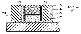
- the fluorescent sensor 10 which is a main functional part of the needle-type fluorescent sensor 4 includes a detection substrate part 20 and a light emitting diode (Light Emitting Diode) which is a light emitting element that generates excitation light E. (Hereinafter also referred to as “LED”), an element 12, a transparent resin layer 15, an indicator layer 16 that generates fluorescence F corresponding to excitation light E and the amount of analyte, and a light shielding layer 19.
- LED Light Emitting Diode
- the detection substrate unit 20 is manufactured by bonding the wiring substrate 30 and the frame substrate 40 in which the through holes 46 are formed. For this reason, the detection substrate unit 20 has a recess 23 having a bottom surface 22 parallel to the first main surface 21 on the first main surface 21. That is, the surface of the wiring substrate 30 is the bottom surface 22 of the recess 23, and the wall surface 45 of the through hole 46 of the frame-shaped substrate 40 is the side surface 24 of the recess 23.
- an insulating layer is appropriately formed on the surface of the detection substrate unit 20 made of, for example, an N-type semiconductor, that is, the wiring substrate 30 and the frame substrate 40, it is not illustrated.
- the LED element 12 is disposed on the bottom surface 22 of the recess 23, and the indicator layer 16 is disposed on the LED element 12 upper side inside the recess 23.
- a reflective layer 12 ⁇ / b> A made of, for example, a highly reflective metal is formed on the bottom and side surfaces of the LED element 12, and the excitation light E is generated only toward the indicator layer 16.
- the LED element 12 having the reflective layer 12A on the bottom surface irradiates the indicator layer 16 with excitation light E having a light quantity about twice that of the LED element without the reflective layer.
- the reflection layer 12A on the side surface can prevent the indicator layer 16 from being irradiated with noise light caused by the excitation light E. Note that the same effect can be obtained when the PD element 13 is not formed in the region of the side surface 24 of the recess 23 facing the side surface of the LED element 12 instead of the reflective layer 12A.
- the light emitting element is not limited to the LED element 12, but can be selected from various types of light emitting elements such as an organic EL element, an inorganic EL element, or a laser diode element.
- the LED element 12 is preferable from the viewpoints of fluorescence transmittance, light generation efficiency, wide wavelength selectivity of the excitation light E, and generation of a small amount of light having a wavelength other than the ultraviolet light that serves as the excitation light E. .
- the transparent resin layer 15 is a second protective layer.
- an epoxy resin, a silicone resin, a transparent amorphous fluororesin, or the like can be used as the second protective layer.
- the second protective layer is selected from materials having characteristics such as electrical insulation, moisture barrier properties, and good transmittance for excitation light E and fluorescence F.
- the characteristic that the fluorescence F is small is an important characteristic of all the transparent materials of the fluorescent sensor 10 except the indicator layer 16.
- the indicator layer 16 generates fluorescence F having a light amount corresponding to the concentration of the analyte 9 by the interaction with the analyte 9 that has entered and the excitation light E.
- the thickness of the indicator layer 16 is set to about several tens ⁇ m to 200 ⁇ m.
- the indicator layer 16 is made of a base material containing a fluorescent dye that generates fluorescence F having an intensity corresponding to the amount of the analyte 9, that is, the concentration of the analyte in the sample.
- the fluorescent dye is selected according to the type of the analyte 9 and can be used for any fluorescent dye that reversibly changes the amount of the fluorescence F generated according to the amount of the analyte 9.
- fluorescence F generated according to the amount of the analyte 9.
- a fluorescent dye such as a ruthenium organic complex, a fluorescent phenylboronic acid derivative, or a substance that reversibly binds to glucose such as fluorescein bound to a protein can be used.
- the fluorescent sensor 10 of the present invention is compatible with various uses such as an oxygen sensor, a glucose sensor, a pH sensor, an immunosensor, or a microorganism sensor, depending on the selection of the fluorescent dye.
- the indicator layer 16 includes, for example, a hydrogel that easily contains water as a base material and contains or is bonded to the fluorescent dye in the hydrogel.
- Hydrogel components include polysaccharides such as methylcellulose or dextran, acrylic hydrogels made by polymerizing monomers such as (meth) acrylamide, methylolacrylamide, or hydroxyethyl acrylate, or urethanes made from polyethylene glycol and diisocyanate. Hydrogel etc. can be used.
- the indicator layer 16 is joined to the transparent resin layer 15 through an adhesive layer made of a silane coupling agent (not shown).
- the indicator layer 16 may be directly bonded to the surface of the LED element 12 without forming the transparent resin layer 15.
- the light shielding layer 19 is a layer formed on the upper surface side of the indicator layer 16 and having a thickness of several tens of ⁇ m or less.
- the light shielding layer 19 prevents the excitation light E and the fluorescence F from leaking to the outside of the fluorescence sensor 10 and at the same time prevents external light from entering the recess 23.
- a photodiode (Photo Diode: hereinafter) that receives fluorescence F and outputs a detection signal.
- An element 13 also referred to as “PD”) is formed. That is, the PD element 13 is provided so as to surround the indicator layer 16 and is formed so that the light receiving surface faces the indicator layer 16.
- the PD element 13 may be formed on the entire side surface 24, but may be formed only in a region facing the indicator layer 16 in order to efficiently receive only the fluorescence F.
- the indicator layer 16 may be formed on all of the four side surfaces 24 or may be formed on only a part of the surfaces.
- the PD element 13 only needs to be formed on at least a part of the side surface 24 of the recess 23.
- the photoelectric conversion element may be a photoconductor (photoconductor) or a phototransistor (PhotoTransistor, PT).
- a silicon oxide layer 42 which is a first protective layer for protecting the PD element 13 and a filter 41 are disposed so as to cover the PD element 13 formed on the side surface 24.
- the filter 41 is formed on the light receiving surface side of the PD element 13 so as to cover the PD element 13.
- the filter 41 is, for example, an absorptive filter that cuts the excitation light E without passing therethrough and allows the fluorescence F having a longer wavelength to pass therethrough.
- a material for such a filter a silicon layer or a silicon carbide layer is suitable.
- the filter 41 may be a band-pass filter that passes only the fluorescence F.
- the frame-shaped substrate 40 transmits a drive signal to the two wires 61 and 62 for transmitting the detection signals output from the electrodes 43 and 44 of the PD element 13 to the main body 2 and the electrode 12B of the LED element.
- the two wirings 63 and 64 are provided.
- the electrode 44 is formed on the surface of the frame-shaped substrate 40, which is an N-type semiconductor, by partially introducing an N-type impurity, such as phosphorus or arsenic, to form a low-resistance region 40H having higher conductivity. ing.
- the material of the frame-like substrate 40 is preferably single crystal silicon in order to form the PD element 13 on the frame-like substrate 40, but may be glass or ceramic.
- the outer wall of the frame-shaped substrate 40 and the bottom surface of the wiring substrate 30, that is, the outer wall of the detection substrate unit 20 and the second main surface 25 are coated with the same material as the light shielding layer 19 or a resin mixed with carbon black, It is preferable to deposit a metal layer.
- the excitation light E generated by the LED element 12 is applied to the fluorescent dye in the indicator layer 16.
- a part of the fluorescence F generated by the interaction of the fluorescent dye with the analyte 9 passes through the filter 41 and reaches the PD element 13 and is converted into a detection signal.
- the fluorescence sensor 10 has a high detection sensitivity because the PD element 13 formed on the side surface 24 surrounding the indicator layer 16 detects the fluorescence F.
- 6A to 6E are partial sectional views of the region of one fluorescent sensor 10, but in an actual process, a large number of elements are collectively formed as a wafer process.
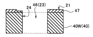
- the conductive (N-type) first silicon wafer 40W is etched through the mask layer 47 to obtain a large number of frame-shaped substrates.
- a pattern, that is, a through hole 46 to be the recess 23 is formed.
- Various known methods can be used for etching.
- the size of the opening of the through hole 46 is designed according to the specifications. However, since the arrangement location is the needle tip portion 5, it is preferable to have an elongated shape such as 150 ⁇ m in length and 500 ⁇ m in width. .
- the side surface 24 of the recess 23 is perpendicular to the first main surface 21, but the side surface may have a predetermined angle, that is, a tapered shape, as will be described later.
- the tapered recess can be produced, for example, by wet etching.
- the PD element 13 is formed on the wall surface 45 (side surface 24 of the recess 23) of the through hole 46. That is, the ion implantation process is performed from four directions in a state where the first silicon wafer 40W on which the mask layer 47A is formed is inclined by 5 degrees to 30 degrees.
- the conditions for implanting boron (B) are acceleration voltage: 10 to 100 keV and implantation amount: about 1 ⁇ 10 15 cm ⁇ 2 .
- a thin oxide layer of 50 to 100 nm may be present on the first silicon wafer 40W.
- a silicon oxide layer 42 and a filter 41 are sequentially formed by the CVD method so as to cover the PD element 13 on the wall surface 45 of the through hole 46 of the first silicon wafer 40W, and further electrodes 43 and 44 are formed. Is done.
- a conductive (N-type) second silicon wafer 30W to be the wiring substrate 30 is prepared.
- Wirings 61 and 62 for transmitting a detection signal from the PD element 13 and wirings 63 and 64 for supplying a driving signal to the LED element 12 are formed on the second silicon wafer 30W by a sputtering method or an evaporation method. Is done.
- the first silicon wafer 40W is turned upside down and joined to the second silicon wafer 30W.
- the through hole 46 of the frame-shaped substrate 40 becomes a recess 23 having the bottom surface 22.
- the LED element 12 and the transparent resin layer 15 are disposed in each of the plurality of recesses 23 of the bonded wafer 20W, and a silane coupling agent or the like is further disposed on the upper side of the transparent resin layer 15.
- the indicator layer 16 is disposed via an adhesive layer as necessary.
- a bonding method using an optically transparent acrylic resin or silicone resin, or various bonding methods such as a flip chip bonding method can be used.
- the bonded wafer 20 ⁇ / b> W is separated into pieces, and the fluorescent sensor 10 is completed. That is, the needle-type fluorescence sensor 4 having the fluorescence sensor 10 at the needle tip 5 is completed.
- the method of manufacturing the fluorescent sensor is not limited to this, and after the separated wiring substrate 30 and the separated frame substrate 40 are joined, the LED element 12 and the like are arranged in the recess 23.
- a method such as setting may be used.
- the first silicon wafer may be processed so that the extended portion of the wiring board 30 constitutes the needle main body portion 6 of the needle portion 7, or the needle main body portion 6 and the fluorescent sensor 10 that are separately manufactured are included.
- the needle portion 7 may be configured by joining the needle tip portion 5.
- the fluorescent sensor 10 according to the present embodiment can be mass-produced in a batch by a wafer process. For this reason, the fluorescence sensor 10 can provide stable quality at low cost.
- the LED element 12 emits pulsed excitation light E having a center wavelength of around 375 nm at intervals of, for example, once every 30 seconds.
- the pulse current to the LED element 12 is 1 mA to 100 mA, and the pulse width of light emission is 10 ms to 100 ms.
- the excitation light E generated by the LED element 12 passes through the transparent resin layer 15 and enters the indicator layer 16.
- the indicator layer 16 emits fluorescence F having an intensity corresponding to the amount of the analyte 9.
- the analyte 9 passes through the light shielding layer 19 and enters the indicator layer 16.
- the fluorescent dye of the indicator layer 16 generates fluorescence F having a longer wavelength, for example, a wavelength of 460 nm with respect to the excitation light E having a wavelength of 375 nm.
- a part of the fluorescence F generated by the indicator layer 16 enters the PD element 13 through the filter 41 and the silicon oxide layer 42. Then, the fluorescence F is photoelectrically converted in the PD element 13 to generate photogenerated charges, and is output as a detection signal. A part of the excitation light E generated by the LED element 12 also enters the side surface 24 of the recess 23, but hardly enters the PD element 13 due to the action of the filter 41.
- a calculation unit (not shown) of the main body 2 performs calculation processing based on a detection signal, that is, a current caused by the photogenerated charge from the PD element 13 or a voltage caused by the accumulated photogenerated charge. And calculate the amount of analyte.
- a detection signal that is, a current caused by the photogenerated charge from the PD element 13 or a voltage caused by the accumulated photogenerated charge.
- the needle-type fluorescent sensor 4 may have a calculation unit or a detection signal processing circuit.
- the fluorescent sensor 10 has the LED element 12 on the bottom surface 22 of the concave portion 23 of the detection substrate portion and the PD element 13 on the side surface 24, and thus has high detection sensitivity despite being ultra-compact.
- the LED element 12 of the fluorescent sensor 10 of the first embodiment is made of a semiconductor 12N made of a gallium nitride compound having a thickness of about 10 ⁇ m formed on a sapphire substrate 12S having a thickness of about 60 to 100 ⁇ m. .
- the thickness of the LED element 12 is 100 ⁇ m and the depth of the recess is 150 ⁇ m, the thickness of the indicator layer 16 of the fluorescent sensor 10 is 50 ⁇ m or less.
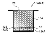
- the LED element 12T of the fluorescence sensor 10A is mainly composed of a semiconductor 12N made of a gallium nitride compound, with most of the sapphire substrate 12S removed from the LED element 12. That is, the thickness of the LED element 12T is about 10 ⁇ m.
- the reflective layer 12AA is also formed on the side surface of the LED element 12T. However, since the LED element 12T is thin, it may be formed only on the bottom surface.
- the thickness of the indicator layer 16A can be 140 ⁇ m, which is larger than the indicator layer 16 of the fluorescent sensor 10.
- the fluorescent sensor 10A has the effect of the fluorescent sensor 10 and can generate more fluorescent F because the indicator layer 16A is thick. For this reason, the fluorescence sensor 10A has higher detection sensitivity.
- the needle-type fluorescence sensor 4B having the fluorescence sensor 10B according to the second embodiment of the present invention will be described. Since the fluorescence sensor 10B of the present embodiment is similar to the fluorescence sensor 10 of the first embodiment, the same components are denoted by the same reference numerals and description thereof is omitted.
- the fluorescence sensor 10B is a PD element 13A that is a first photoelectric conversion element formed on the side surface 24 (the wall surface 45 of the through hole 46 of the frame-shaped substrate 40) of the recess 23 of the detection substrate unit 20B.
- the PD element 13B which is the second photoelectric conversion element, is also formed on the bottom surface 22 of the recess 23 (the upper surface of the wiring board 30B).
- a silicon oxide layer 42B which is a third protective layer for protecting the PD element 13B, and a filter 41B are disposed so as to cover the PD element 13B formed on the bottom surface 22.
- the silicon oxide layer 42B has the same function as the silicon oxide layers 42 and 42A, and the filter 41B has the same function as the filters 41 and 41A.
- the reflective layer 12A1 of the LED element 12 is only formed on the side surface and is not formed on the bottom surface.
- the LED element 12 is a light emitting element that transmits the fluorescence F.
- the central portions of the PD element 13B, the LED element 12, and the indicator layer 16 are formed in the same region on the upper side of the wiring board 30B.
- a large number of PD elements 13B and respective wirings 60 are formed on the surface of the second silicon wafer to be the wiring substrate 30B.
- a silicon oxide layer 42B having a thickness of several tens to several hundreds of nanometers serving as a first protective layer is formed on the surface of the PD element 13B.
- a filter 41B made of polycrystalline silicon or the like is formed on the surface of the silicon oxide layer 42B.
- the subsequent steps are the same as the manufacturing steps of the fluorescent sensor 10 already described. Note that the detection signal of the PD element 13 ⁇ / b> B is transmitted to the main body 2 via the wirings 65 and 66.
- the fluorescence sensor 10B In the fluorescence sensor 10B, a part of the fluorescence F generated by the indicator layer 16 reaches the PD element 13B through the LED element 12, so that the PD element 13B generates a detection signal B. That is, the LED element 12 that does not have a reflective layer on the bottom surface transmits the fluorescence F.
- the fluorescent sensor 10B outputs not only the detection signal A output from the PD element 13A but also the detection signal B output from the PD element 13B to the main body 2.
- the fluorescence sensor 10B has the effect that the fluorescence sensor 10 has, and further has higher detection sensitivity.
- the PD element 13B does not have to be formed in a region facing the bottom surface of the LED element 12. That is, the PD element 13 ⁇ / b> B only needs to be formed on at least a part of the bottom surface 22 of the recess 23.
- a thin layered LED element similar to the LED element 12T of the modified example of the first embodiment may be used.
- the detection signal A output from the PD element 13A and the detection signal B output from the PD element 13B are sent to the main body 2 via separate wirings 61, 62, 65, 66, respectively. Output to.
- the fluorescence sensor 10 ⁇ / b> C uses the two wires 67 and 68 to send the combined detection signal of the detection signal A output from the PD element 13 ⁇ / b> A and the detection signal B output from the PD element 13 ⁇ / b> B to the main body 2. Output.
- a part of the PD element 13B formed on the wiring board 30C extends to a position directly below the frame substrate 40, and is connected to the wiring 68 of the PD element 13A immediately below. Further, the low resistance region 30H of the wiring substrate 30C formed by the same method as that of the low resistance region 40H is connected to the common wiring 67 immediately below the low resistance region 40H of the frame substrate 40.
- flip-chip mounting technology or solder connection technology is used for electrical connection.
- the fluorescent sensor 10C has the effect of the fluorescent sensor 10B and the like, and has a smaller size because the number of wirings 60 for outputting detection signals is as small as two.
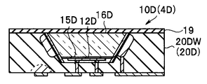
- a needle-type fluorescence sensor 4D having a fluorescence sensor 10D according to a modification of the third embodiment of the present invention will be described. Since the fluorescence sensor 10D of this modification is similar to the fluorescence sensor 10 of the first embodiment, the same components are denoted by the same reference numerals, and description thereof is omitted.
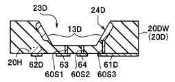
- the detection substrate portion 20D of the fluorescence sensor 10D is integrally manufactured by a silicon wafer 20DW that is a semiconductor substrate. That is, the recess 23D of the detection substrate unit 20D is a recess formed in the first main surface 21 of the silicon wafer 20DW, for example, by an etching method.
- FIGS. 10A to 10E are partial cross-sectional views of the region of one fluorescent sensor 10D, but in an actual process, a large number of elements are collectively formed as a wafer process.
- a mask layer 27 is formed on the first main surface 21 of the silicon wafer 20DW. Then, as shown in FIG. 10B, a recess 23D having a bottom surface 22D parallel to the first main surface 21 is formed by an etching method.
- etching method a wet etching method using a tetramethylammonium hydroxide (TMAH) aqueous solution, a potassium hydroxide (KOH) aqueous solution, or the like is preferable, but dry etching such as reactive ion etching (RIE) or chemical dry etching (CDE) is used.
- TMAH tetramethylammonium hydroxide
- KOH potassium hydroxide
- CDE chemical dry etching
- the PD element 13D is formed on the side surface 24D of the recess 23D.
- the concave portion 23D having the tapered side surface 24D has a larger area for forming the PD element than the concave portion 23 having the vertical side surface 24, and the PD element 13D can be easily formed on the side surface 24D of the concave portion 23D.
- wirings 63 and 64 for driving signals of the LED element 12D, wirings 61D and 62D for detection signals of the PD element 13D, and the like are formed. Note that the through wirings 60S1, 60S2, and 60S3 for the LED element 12D and the PD element 13D may be formed before the PD element 13D is formed.
- the low resistance region 20H is formed by the same method as the low resistance region 40H.
- a silicon oxide layer 42D and a filter 41D are disposed so as to cover the PD element 13D on the side surface 24D.
- the silicon oxide layer 42D has the same configuration and function as the silicon oxide layer 42
- the filter 41D has the same configuration and function as the filter 41.
- the LED element 12D having the reflective layer 12AD is disposed on the bottom surface 22D of the recess 23D, and the indicator layer 16D is disposed via the transparent resin layer 15D. Further, the fluorescence sensor 10D is completed by separating the silicon wafer 20DW on which the light shielding layer 19D is formed.
- the side surface of the recess may be perpendicular to the first main surface 21 as in the fluorescent sensor 10.
- the LED element 12D of the fluorescence sensor 10D of the third embodiment is a thin layered LED element similar to the LED element 12T of the modification of the first embodiment.
- Fluorescent sensor 10D has the effects of fluorescent sensor 10 and the like, and is easy to manufacture and more sensitive.
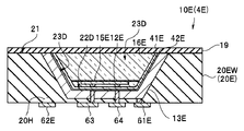
- a PD element 13E which is a photoelectric conversion element, is formed on the side surface 24D of the recess 23D and the bottom surface 22D of the recess 23D of the detection substrate unit 20D.
- the PD element 13E is simultaneously formed on the side surface 24D and the bottom surface 22D of the recess 23D of the silicon wafer 20EW on which the recess 23D having the bottom surface 22D parallel to the first main surface 21 is formed. That is, the PD element formed on the side surface 24D and the PD element formed on the bottom surface are an integrated PD element 13E.
- a silicon oxide layer 42E serving as a first protective layer of the PD element 13E is formed.
- a filter 41E made of polycrystalline silicon or the like is formed on the surface of the silicon oxide layer 42E.
- the subsequent steps are the same as the manufacturing method of the fluorescence sensor 10D of the third embodiment, but the LED element 12E does not have a reflective layer on the bottom surface.
- the fluorescence sensor 10E of this embodiment has high detection sensitivity because the PD element 13E also detects the fluorescence F that has passed through the LED element 12E, similarly to the fluorescence sensor 10B.
- the PD element 13E integrally formed on the side surface 24D and the bottom surface 22D is not only easy to form, but also requires two wiring lines 61E and 62E for detection signals. Further, the silicon oxide layer 42E and the filter 41E can be integrally formed on the side surface 24D and the bottom surface 22D.
- the PD element 13D may be divided into a plurality of regions, and the detection signals in the respective regions may be transmitted to the main body 2 through separate wirings.
- Fluorescent sensor 10E has the effects of fluorescent sensor 10D, and is highly sensitive and easy to manufacture.
- a needle-type fluorescence sensor 4F (4F1, 4F2) having the fluorescence sensor 10F (10F1, 10F2) of the fourth embodiment of the present invention will be described. Since the fluorescent sensor 10F according to the present embodiment is similar to the fluorescent sensor 10 according to the first embodiment, the same components are denoted by the same reference numerals and description thereof is omitted.
- the fluorescence sensor 10 ⁇ / b> F has a high transmittance in the wavelength region of the fluorescence F among the light generated by the LED element 12, and has a low transmittance in the wavelength region longer than the fluorescence F and a long wavelength that cuts long wavelength light including excitation light.
- a cut filter 51 is provided.
- the LED element 12 generates excitation light E having a center wavelength of around 375 nm, for example, but may contain slightly longer-wavelength light than the fluorescence F.
- minute light emission may appear from the LED element 12 in a wide wavelength range on the long wavelength side.
- the light receiving sensitivity of the PD element 13 is high on the long wavelength side, and the transmittance of the filter is also high on the long wavelength side.
- the longer wavelength component light than the fluorescence F of the LED element 12 does not contribute to the generation of the fluorescence of the indicator layer 16 but also causes a large noise component of the detection signal even if it is weak.
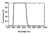
- FIG. 12 shows an example of transmittance characteristics of the long wavelength cut filter 51 suitable for detecting the fluorescence F having a peak wavelength of 475 nm, a short wavelength end of 425 nm, and a long wavelength end of 650 nm.
- the long wavelength cut filter 51 is transparent in the wavelength region of the fluorescence F.
- the long wavelength cut filter 51 is, for example, a dielectric multilayer film formed by laminating multiple dielectrics such as LaF 3 , Al 2 O 3 , Pr 2 O 3 , Ta 2 O 3 , TiO 2, or Nb 2 O 5. It is.
- the long wavelength cut filter 51A is disposed above the LED element 12F1 having the reflective layer 12F1A.
- the long wavelength cut filters 51B1 and 51B2 are above and below the LED element 12, respectively. Arranged.
- the long wavelength cut filter is not limited to a method of inserting a solid filter such as a dielectric multilayer film, but a method of applying / solidifying a fluid resin or a method of vapor deposition on both surfaces of the LED element 12 May be formed.
- the fluorescence sensor 10F of the present embodiment since the long wavelength light generated by the LED element 12 is cut by the long wavelength cut filter 51, noise light that becomes an offset output is removed, so that the S / N of the detection signal is improves. For this reason, the fluorescence sensor 10F has the effect which the fluorescence sensor 10 grade
Abstract
蛍光センサ10は、第1の主面21に第1の主面21と平行な底面22のある凹部23があり、凹部23の側面24に、蛍光Fを受光し検出信号を出力するPD素子13が形成されている検出基板部20と、検出基板部20の凹部23の底面22に配設された、励起光Eを発生するLED素子12と、LED素子12の上の凹部23の内部に配設された励起光Eとアナライト量とに応じた蛍光Fを発生するインジケータ層16と、を具備する。
Description
本発明の実施形態は、アナライトの濃度を計測する蛍光センサに関し、特に半導体製造技術およびMEMS技術を用いて作製される微小蛍光分光光度計である蛍光センサに関する。
液体中のアナライトすなわち被計測物質の存在確認、または、濃度を測定するための様々な分析装置が開発されている。例えば、一定容量の透明容器に、アナライトの存在によって性質が変化し蛍光を発生する蛍光色素と、アナライトを含む被計測溶液とを注入し、励起光Eを照射し蛍光色素からの蛍光強度を計測することによりアナライト濃度を計測する蛍光分光光度計が知られている。
小型の蛍光分光光度計は、光検出器と蛍光色素を含有したインジケータ層とを有している。そして、被計測溶液中のアナライトが進入可能なインジケータ層に光源からの励起光Eを照射することで、インジケータ層内の蛍光色素が被計測溶液中のアナライト濃度に応じた光量の蛍光を発生し、その蛍光を光検出器が受光する。光検出器は光電変換素子であり、受光した光量に応じた電気信号を出力する。この電気信号から被計測溶液中のアナライト濃度が測定される。
近年、微量試料中のアナライトを計測するために、半導体製造技術およびMEMS技術を用いて作製される微小蛍光分光光度計が提案されている。以下、微小蛍光光度計のことを。「蛍光センサ」と呼ぶ。
例えば、図1および図2に示す蛍光センサ110が米国特許第5039490号明細書に開示されている。蛍光センサ110は、励起光Eが透過可能な透明支持基板101と、蛍光を電気信号に変換する光電変換素子部103と、励起光Eを集光する集光機能部105Aとを有する光学板状部105と、アナライト9と相互作用することによって励起光Eの入射により蛍光を発生するインジケータ層106と、カバー層109と、から構成されている。
光電変換素子部103としては、例えばシリコンからなる基板103Aに形成された光電変換素子である。基板103Aは励起光Eを透過しない。このため、蛍光センサ110は、光電変換素子部103の周囲に励起光Eが透過可能な空隙領域120を有している。
すなわち、空隙領域120を透過し光学板状部105に入射した励起光Eだけが、光学板状部105の作用により、インジケータ層106中の、光電変換素子部103の上部付近に集光される。集光された励起光E2と、インジケータ層106の内部に進入したアナライト9の相互作用により、蛍光Fが発生する。発生した蛍光Fの一部は光電変換素子部103に入射し、光電変換素子部103において蛍光強度、つまりアナライト9の濃度に比例した電流または電圧などの信号が発生する。なお励起光Eは、光電変換素子部103を覆うフィルタ(不図示)の作用により、光電変換素子部103には入射しない。
以上の説明のように、蛍光センサ110は、透明支持基板101上に、光電変換素子部103であるフォトダイオードを励起光Eの通路である空隙領域120を確保した基板103A上に形成し、その上側に、光学板状部105およびインジケータ層106が積層されている。
しかし、上記の公知の蛍光センサ110は、励起光Eの通路である空隙領域120と光電変換素子部103の領域とを、同一平面上に有する。このため、より多くの励起光Eをインジケータ層106に導光するために通路である空隙領域120の面積を広くすると、光電変換素子部103の面積が狭くなるため、蛍光センサの感度を高めることにはならない。反対に光電変換素子部103の検出感度を高くするために光電変換素子部103の面積を広くすると、励起光Eの通路である空隙領域120の面積が狭くなりインジケータ層106に導光する励起光Eが減少してしまうために、やはり蛍光センサの感度を高めることにはならない。すなわち、蛍光センサ110では、高い検出感度を得ることは容易ではなかった。
本発明の実施形態は、検出感度の高い蛍光センサを提供することを目的とする。
本発明の一態様の蛍光センサは、第1の主面に前記第1の主面と平行な底面のある凹部があり、前記凹部の側面の少なくとも一部に、蛍光を受光し検出信号を出力する光電変換素子が、形成されている検出基板部と、前記検出基板部の前記凹部の前記底面に配設された、励起光を発生する発光素子と、前記発光素子の上側の前記凹部の内部に配設された、前記励起光とアナライト量とに応じた前記蛍光を発生するインジケータ層と、を具備する。
<第1実施形態>
以下、本発明の第1実施形態の蛍光センサ10について説明する。
以下、本発明の第1実施形態の蛍光センサ10について説明する。
図3に示すように、蛍光センサ10を有する針型蛍光センサ4は、本体部2およびレシーバー3と、ともにセンサシステム1を構成する。
すなわち、センサシステム1は、針型蛍光センサ4と、本体部2と、本体部2からの信号を受信し記憶するレシーバー3と、を有する。本体部2とレシーバー3との間の信号の送受信は無線または有線で行われる。
針型蛍光センサ4は、主要機能部である蛍光センサ10を有する針先端部5と細長い針本体部6とを有する針部7と、針本体部6の後端部と一体化したコネクタ部8と、を具備する。針先端部5、針本体部6、コネクタ部8は同一材料により一体形成されていてもよい。
コネクタ部8は、本体部2の嵌合部2Aと着脱自在に嵌合する。針型蛍光センサ4の蛍光センサ10から延設された複数の配線60は、コネクタ部8が本体部2の嵌合部2Aと機械的に嵌合することにより、本体部2と電気的に接続される。なお、以下、複数の配線60のそれぞれを配線61(~68)で示す。
図示しないが、本体部2は、蛍光センサ10からの検知信号を処理する演算部と、レシーバー3との間で無線信号を送受信するための無線アンテナと、電池等と、を有する。なお、レシーバー3との間を有線送受信する場合には、本体部2は無線アンテナに代えて信号線を有する。
蛍光センサ10は感染防止等のために使用後は処分される使い捨て(ディスポ)部であるが、本体部2およびレシーバー3は繰り返し再使用されるリユース部である。なお、本体部2が必要な容量のメモリ部を有する場合にはレシーバー3は不要である。
針型蛍光センサ4は本体部2と嵌合した状態で、被検者自身が体表面から穿刺して針先端部5が体内に留置される。そして、例えば体液中のグルコース濃度を連続して測定し、レシーバー3のメモリに記憶する。すなわち、本実施の形態の蛍光センサ10は連続使用期間が一週間程度の短期皮下留置型のセンサである。
そして、図4、図5に示すように、針型蛍光センサ4の主要機能部である蛍光センサ10は、検出基板部20と、励起光Eを発生する発光素子である発光ダイオード(Light Emitting Diode:以下「LED」ともいう)素子12と、透明樹脂層15と、励起光Eとアナライト量とに応じた蛍光Fを発生するインジケータ層16と、遮光層19と、を有する。
検出基板部20は、配線基板30と、貫通孔46が形成された枠状基板40と、を接合することにより作製されている。このため、検出基板部20には、第1の主面21に、第1の主面21と平行な底面22のある凹部23がある。すなわち、配線基板30の表面が、凹部23の底面22であり、枠状基板40の貫通孔46の壁面45が、凹部23の側面24である。なお、例えばN型半導体からなる検出基板部20、すなわち配線基板30および枠状基板40の表面等には適宜、絶縁層が形成されているが、図示はしない。
LED素子12は、凹部23の底面22に配設されており、インジケータ層16は、凹部23の内部のLED素子12上側に配設されている。なお、LED素子12の底面および側面には、例えば、高反射率の金属からなる反射層12Aが形成されており、インジケータ層16に向けてのみ励起光Eを発生する。底面に反射層12Aを有するLED素子12は、反射層のないLED素子の約2倍の光量の励起光Eをインジケータ層16に向けて照射する。また側面の反射層12Aにより、励起光Eに起因するノイズ光のインジケータ層16への照射を防止できる。なお、反射層12Aに替えて、LED素子12の側面と対向する凹部23の側面24の領域にPD素子13を形成しない場合にも同様の効果を得ることができる。
発光素子としては、LED素子12に限られるものではなく、有機EL素子、無機EL素子、またはレーザダイオード素子など多様な種類の発光素子の中から選択される。そして、蛍光透過率、光発生効率、励起光Eの波長選択性の広さ、および励起光Eとなる紫外線以外の波長の光を僅かしか発生しないことなどの観点からは、LED素子12が好ましい。
透明樹脂層15は第2の保護層である。第2の保護層としては、エポキシ樹脂、シリコーン樹脂、または透明な非晶性フッ素樹脂などが使用可能である。第2の保護層は、電気的絶縁性を有すること、水分遮断性を有すること、励起光Eおよび蛍光Fに対して良好な透過率を有すること、などの特性を有する材料から選択される。
第2の保護層の特性として、励起光Eが照射されても層中での蛍光Fの発生が小さいことが重要である。なお、この蛍光Fが小さいという特性は、インジケータ層16を除いた蛍光センサ10の全ての透明材料の重要特性であることは言うまでもない。
インジケータ層16は、進入してきたアナライト9との相互作用および励起光Eによりアナライト9の濃度に応じた光量の蛍光Fを発生する。インジケータ層16の層厚は数十μm~200μm程度に設定されている。インジケータ層16は、アナライト9の量、すなわち試料中のアナライト濃度に応じた強度の蛍光Fを発生する蛍光色素が含まれたベース材料から構成されている。
蛍光色素は、アナライト9の種類に応じて選択され、アナライト9の量に応じて発生する蛍光Fの光量が可逆的に変化する蛍光色素ならば、どのようなものにも使用できる。例えば生体内の水素イオン濃度または二酸化炭素を測定する場合には、ヒドロキシピレントリスルホン酸誘導体、糖類を測定する場合には蛍光残基を有するフェニルボロン酸誘導体、カリウムイオンを測定する場合には蛍光残基を有するクラウンエーテル誘導体などを用いることができる。そして、グルコースのような糖類を測定する場合には、蛍光色素として、ルテニウム有機錯体、蛍光フェニルボロン酸誘導体、または蛋白と結合したフルオレセイン等のグルコースと可逆結合する物質を用いることができる。
以上の説明のように、本発明の蛍光センサ10は、蛍光色素の選択によって、酸素センサ、グルコースセンサ、pHセンサ、免疫センサ、または微生物センサなど、多様な用途に対応している。
インジケータ層16は、例えば、含水し易いハイドロゲルをベース材料として、ハイドロゲル内に上記蛍光色素を含有するまたは結合されている。ハイドロゲルの成分としてはメチルセルロースもしくはデキストランなどの多糖類、(メタ)アクリルアミド、メチロールアクリルアミド、もしくはヒドロキシエチルアクリレート等のモノマーを重合して作製するアクリル系ハイドロゲル、またはポリエチレングリコールとジイソシアネートから作製するウレタン系ハイドロゲルなどを用いることができる。
インジケータ層16は、透明樹脂層15上に、図示していないシランカップリング剤などよりなる接着層を介して接合されている。なお、透明樹脂層15を形成しないで、インジケータ層16がLED素子12の表面に、直接、接合された構造であってもよい。
遮光層19は、インジケータ層16の上部表面側に形成された、厚さが数十μm以下の層である。遮光層19は、励起光Eおよび蛍光Fが蛍光センサ10の外部へ漏光するのを防止すると同時に、外光が凹部23に進入するのを防止する。
一方、枠状基板40の貫通孔46の壁面45、すなわち検出基板部20の凹部23の側面24には、蛍光Fを受光し検出信号を出力する光電変換素子であるフォトダイオード(Photo Diode:以下「PD」ともいう)素子13が形成されている。すなわち、PD素子13は、インジケータ層16を囲むように設けられ、受光面がインジケータ層16に向くように形成されている。
PD素子13は、側面24の全体に形成されていてもよいが、蛍光Fのみを効率的に受光するために、インジケータ層16との対向領域にのみに形成してもよい。またインジケータ層16は、4面ある側面24の全てに形成されていてもよいし、一部の面のみに形成されていてもよい。
すなわち、PD素子13は、凹部23の側面24の少なくとも一部に、形成されていればよい。
光電変換素子としては、フォトコンダクタ(光導電体)、またはフォトトランジスタ(Photo Transistor、PT)などでもよい。
側面24に形成されたPD素子13を覆うように、PD素子13を保護する第1の保護層である酸化シリコン層42と、フィルタ41と、が配設されている。フィルタ41はPD素子13の受光面側に、PD素子13を覆うように形成されている。
フィルタ41は、例えば、励起光Eは通さずカットし、それよりも長波長の蛍光Fは通す吸収型フィルタである。このようなフィルタの材料としては、シリコン層または炭化シリコン層が好適である。なお、フィルタ41として蛍光Fのみを通すバンドパスフィルタであってもよい。
枠状基板40は、PD素子13の電極43、44から出力される検出信号を本体部2に伝達するための2本の配線61、62、およびLED素子の電極12Bに駆動信号を伝達するための2本の配線63、64を有する。電極44はN型半導体である枠状基板40の表面に部分的にN型不純物、例えばリンまたはヒ素等を導入して、より導電率の高い低抵抗領域40Hを形成し、その上に形成されている。
枠状基板40の材料は、PD素子13を枠状基板40に形成するためには単結晶シリコンが好ましいが、ガラスまたはセラミック等でもよい。
インジケータ層16が発生する蛍光Fが外部に漏光することを防ぎ、外光が凹部23に進入するのを防ぐために遮光することが好ましい。すなわち、枠状基板40の外壁および配線基板30の底面、すなわち、検出基板部20の外壁および第2の主面25を、遮光層19と同じ材料またはカーボンブラックを配合した樹脂でコーティングしたり、金属層を蒸着したりすることが好ましい。
LED素子12が発生した励起光Eは、インジケータ層16中の蛍光色素に照射される。そして、蛍光色素がアナライト9との相互作用により発生した蛍光Fの一部は、フィルタ41を通過してPD素子13に到達し、検出信号に変換される。
蛍光センサ10は、インジケータ層16を取り囲む側面24に形成されたPD素子13により蛍光Fを検出するために、検出感度が高い。
次に、蛍光センサ10の製造方法について簡単に説明する。なお、図6A~図6Eでは1個の蛍光センサ10の領域の部分断面図であるが、実際の工程では、ウエハプロセスとして一括して多数の素子を形成する。
最初に、図6Aに示すように、枠状基板40の作製では、導電性(N型)の第1のシリコンウエハ40Wに対して、マスク層47を介してエッチングが行われ、多数の枠状パターン、すなわち凹部23となる貫通孔46が形成される。エッチングには公知の各種の方法を用いることができる。
なお、貫通孔46の開口の大きさは仕様に応じて設計されるが、配設箇所が針先端部5であるために、例えば、縦150μm、横500μmのように細長い形状であることが好ましい。
また、蛍光センサ10では、凹部23の側面24は第1の主面21に垂直であるが、後述するように、側面は所定の角度、すなわちテーパーのある形状であってもよい。テーパー形状の凹部は例えばウエットエッチングにより作製することができる。
次に、図6Bに示すように、貫通孔46の壁面45(凹部23の側面24)にPD素子13が形成される。すなわち、マスク層47Aが形成された第1のシリコンウエハ40Wを5度~30度に傾けた状態で、4方向からイオン注入処理が行われる。例えば、ほう素(B)を注入する場合の条件は、加速電圧:10~100keV、注入量:1×1015cm-2程度である。このとき第1のシリコンウエハ40Wに、50~100nmの薄い酸化物層があってもよい。
そして、第1のシリコンウエハ40Wの貫通孔46の壁面45のPD素子13を覆うように、酸化シリコン層42と、フィルタ41と、が順にCVD法により、形成され、さらに電極43、44が形成される。
別途、配線基板30となる導電性(N型)の第2のシリコンウエハ30Wが準備される。第2のシリコンウエハ30Wには、PD素子13からの検出信号を送信するための配線61、62およびLED素子12に駆動信号を供給するための配線63、64がスパッタ法または蒸着法等により形成される。
図6Cに示すように、第1のシリコンウエハ40Wが上下反転されて、第2のシリコンウエハ30Wと接合される。
すると図6Dに示すように、2枚のウエハが接合された接合ウエハ20Wでは、枠状基板40の貫通孔46は、底面22のある凹部23となる。
そして、図6Eに示すように、接合ウエハ20Wの複数の凹部23のそれぞれの内部に、LED素子12および透明樹脂層15が配設され、さらに透明樹脂層15の上側にシランカップリング剤などの接着層を必要に応じて介して、インジケータ層16が配設される。
LED素子12の配設には、光学的に透明なアクリル樹脂もしくはシリコーン樹脂などを使用した接着法、または、フリップチップボンディング法などの各種接合法などの方法が使用可能である。
最後に遮光層19がインジケータ層16を覆うように形成された後、接合ウエハ20Wが個片化されて、蛍光センサ10が完成する。すなわち、蛍光センサ10を針先端部5に有する針型蛍光センサ4が完成する。
蛍光センサの製造方法としては、これに限られるものではなく、個片化された配線基板30と、個片化された枠状基板40とを接合した後に、凹部23にLED素子12等を配設する等の方法を用いてもよい。
また、配線基板30の延設部が針部7の針本体部6を構成するように第1のシリコンウエハを加工してもよいし、別途作製した針本体部6と、蛍光センサ10を有する針先端部5とを接合して針部7を構成してもよい。
以上の説明のように、本実施の形態の蛍光センサ10は、ウエハプロセスにより一括大量生産が可能である。このため、蛍光センサ10は、安価に安定した品質を提供できる。
次に、図5を参照して、蛍光センサ10の動作を説明する。
LED素子12は、例えば30秒に1回の間隔で中心波長が375nm前後の励起光Eをパルス発光する。例えば、LED素子12へのパルス電流は1mA~100mAであり、発光のパルス幅は10ms~100msである。
LED素子12が発生した励起光Eは透明樹脂層15を通過して、インジケータ層16に入射する。インジケータ層16は、アナライト9の量に対応した強度の蛍光Fを発する。なお、アナライト9は遮光層19を通過して、インジケータ層16に進入する。インジケータ層16の蛍光色素は波長375nmの励起光Eに対して、より長波長の例えば波長460nmの蛍光Fを発生する。
インジケータ層16が発生した蛍光Fの一部は、フィルタ41と酸化シリコン層42と介して、PD素子13に入射する。そして蛍光Fは、PD素子13において光電変換され光発生電荷を生じることで、検出信号として出力される。なお、LED素子12が発生する励起光Eも一部は、凹部23の側面24に入射するが、フィルタ41の作用によりPD素子13へは殆ど入射しない。
蛍光センサ10では、本体部2の演算部(不図示)が検出信号、すなわち、PD素子13からの光発生電荷に起因する電流または蓄積した光発生電荷に起因する電圧をもとに演算処理を行い、アナライト量を算出する。なお、針型蛍光センサ4が演算部または検出信号処理回路等を有していてもよい。
蛍光センサ10は、検出基板部の凹部23の底面22にLED素子12を有し、側面24にPD素子13を有するため、超小型であるにも関わらず、検出感度が高い。
<第1実施形態の変形例>
次に、本発明の第1実施形態の変形例の蛍光センサ10Aを有する針型蛍光センサ4Aについて説明する。本変形例の蛍光センサ10Aは第1実施形態の蛍光センサ10と類似しているため同じ構成要素には同じ符号を付し説明は省略する。
次に、本発明の第1実施形態の変形例の蛍光センサ10Aを有する針型蛍光センサ4Aについて説明する。本変形例の蛍光センサ10Aは第1実施形態の蛍光センサ10と類似しているため同じ構成要素には同じ符号を付し説明は省略する。
図7Aに示すように、第1実施形態の蛍光センサ10のLED素子12は、60~100μm程度の厚さのサファイア基板12Sに形成された厚み10μm程度の窒化ガリウム系化合物からなる半導体12Nからなる。
このため、例えば、LED素子12の厚さが100μm、凹部の深さが150μmの場合、蛍光センサ10のインジケータ層16の厚さは50μm以下である。
これに対して、図7Bに示すように、蛍光センサ10AのLED素子12Tは、LED素子12から大部分のサファイア基板12Sが除去され、窒化ガリウム系化合物からなる半導体12Nを主体とする。すなわち、LED素子12Tの厚さは、10μm程度である。なお、反射層12AAはLED素子12Tの側面にも形成されているが、LED素子12Tの厚さが薄いため底面のみに形成してもよい。
蛍光センサ10Aでは、例えば、凹部の深さが150μmの場合、インジケータ層16Aの厚さを140μmと、蛍光センサ10のインジケータ層16よりも厚くすることができる。
蛍光センサ10Aは、蛍光センサ10が有する効果を有し、さらにインジケータ層16Aが厚いために、より多くの蛍光Fを発生することができる。このために、蛍光センサ10Aは、より検出感度が高い。
<第2実施形態>
次に、本発明の第2実施形態の蛍光センサ10Bを有する針型蛍光センサ4Bについて説明する。本実施形態の蛍光センサ10Bは第1実施形態の蛍光センサ10と類似しているため同じ構成要素には同じ符号を付し説明は省略する。
次に、本発明の第2実施形態の蛍光センサ10Bを有する針型蛍光センサ4Bについて説明する。本実施形態の蛍光センサ10Bは第1実施形態の蛍光センサ10と類似しているため同じ構成要素には同じ符号を付し説明は省略する。
図8に示すように、蛍光センサ10Bは、検出基板部20Bの凹部23の側面24(枠状基板40の貫通孔46の壁面45)に形成された第1の光電変換素子であるPD素子13Aに加えて、凹部23の底面22(配線基板30Bの上面)にも第2の光電変換素子であるPD素子13Bが形成されている。
底面22に形成されたPD素子13Bを覆うように、PD素子13Bを保護する第3の保護層である酸化シリコン層42Bと、フィルタ41Bと、が配設されている。酸化シリコン層42Bは酸化シリコン層42、42Aと同じ機能を有し、フィルタ41Bはフィルタ41、41Aと同じ機能を有する。なお、LED素子12の反射層12A1は側面のみで底面には形成されていない。また、LED素子12は、蛍光Fを透過する発光素子である。
そして、PD素子13Bと、LED素子12と、インジケータ層16のそれぞれの中央部が配線基板30Bの上側の同一領域内に形成されている。
蛍光センサ10Bの製造工程では、配線基板30Bとなる第2のシリコンウエハの表面には、多数のPD素子13Bと、それぞれの配線60(61~66)が形成される。そしてPD素子13Bの表面に第1の保護層となる数十~数百nmの厚さを有する酸化シリコン層42Bが形成される。さらに酸化シリコン層42Bの表面に、多結晶シリコン等からなるフィルタ41Bが形成される。
以降の工程はすでに説明した蛍光センサ10の製造工程と同様である。なお、PD素子13Bの検出信号は配線65、66を介して本体部2に伝達される。
蛍光センサ10Bでは、インジケータ層16が発生した蛍光Fの一部は、LED素子12を通ってPD素子13Bに到達するために、PD素子13Bは検出信号Bを発生する。すなわち、底面に反射層を有していないLED素子12は蛍光Fを透過する。
蛍光センサ10Bは、PD素子13Aが出力する検出信号Aだけでなく、PD素子13Bが出力する検出信号Bも、本体部2に出力する。
このため、蛍光センサ10Bは、蛍光センサ10が有する効果を有し、さらに、より検出感度が高い。
なお、LED素子12の大きさが、PD素子13Bよりも小さい場合には、LED素子12の底面にも反射層を形成してもよい。この場合には、蛍光Fの一部は、反射層12Aにより反射されてしまうためにPD素子13Bには入射しない。しかし、LED素子12からの励起光Eに起因するPD素子13Bの検出信号のノイズ光成分を、より減ずることができる。
また、ノイズ光成分を減ずるために、LED素子12の底面と対向する領域にはPD素子13Bを形成しなくともよい。すなわち、PD素子13Bは、凹部23の底面22の少なくとも一部に、形成されていればよい。
また、第2実施形態の蛍光センサ10Bにおいても、第1実施形態の変形例のLED素子12Tと同様の薄層化LED素子を用いてもよい。
<第2実施形態の変形例>
次に、本発明の第2実施形態の変形例の蛍光センサ10Cを有する針型蛍光センサ4Cについて説明する。本変形例の蛍光センサ10Cは第2実施形態の蛍光センサ10Bと類似しているため同じ構成要素には同じ符号を付し説明は省略する。
次に、本発明の第2実施形態の変形例の蛍光センサ10Cを有する針型蛍光センサ4Cについて説明する。本変形例の蛍光センサ10Cは第2実施形態の蛍光センサ10Bと類似しているため同じ構成要素には同じ符号を付し説明は省略する。
第2実施形態の蛍光センサ10Bは、PD素子13Aが出力する検出信号Aと、PD素子13Bが出力する検出信号Bとを、それぞれ別の配線61、62、65、66を介して本体部2に出力した。
これに対して、蛍光センサ10Cは、PD素子13Aが出力する検出信号Aと、PD素子13Bが出力する検出信号Bとの合算検出信号を2本の配線67、68を用いて本体部2に出力する。
すなわち、図9に示すように、配線基板30Cに形成されたPD素子13Bは、その一部分が枠状基板40の直下まで延設され、PD素子13Aの配線68と直下で接続されている。また、低抵抗領域40Hと同様の方法で形成された配線基板30Cの低抵抗領域30Hは、枠状基板40の低抵抗領域40Hの直下で共通の配線67と接続されている。
電気的接続箇所には、例えばフリップチップ実装技術または半田接続技術を用いて行われる。
蛍光センサ10Cは、蛍光センサ10B等が有する効果を有し、さらに検出信号を出力するための配線60の数が2本と少ないため、より小型である。
<第3実施形態>
次に、本発明の第3実施形態の変形例の蛍光センサ10Dを有する針型蛍光センサ4Dについて説明する。本変形例の蛍光センサ10Dは第1実施形態の蛍光センサ10等と類似しているため同じ構成要素には同じ符号を付し説明は省略する。
次に、本発明の第3実施形態の変形例の蛍光センサ10Dを有する針型蛍光センサ4Dについて説明する。本変形例の蛍光センサ10Dは第1実施形態の蛍光センサ10等と類似しているため同じ構成要素には同じ符号を付し説明は省略する。
蛍光センサ10Dの検出基板部20Dは、半導体基板であるシリコンウエハ20DWにより一体的に作製されている。すなわち、検出基板部20Dの凹部23Dは、例えばエッチング法によりシリコンウエハ20DWの第1の主面21に形成された凹部である。
次に、図10A~図10Eを用いて、蛍光センサ10Dの製造方法について説明する。なお、図10A~図10Eでは1個の蛍光センサ10Dの領域の部分断面図であるが、実際の工程では、ウエハプロセスとして一括して多数の素子を形成する。
図10Aに示すように、シリコンウエハ20DWの第1の主面21にマスク層27が作製される。そして、図10Bに示すように、エッチング法により、第1の主面21と平行な底面22Dのある凹部23Dが形成される。
エッチング法としては、水酸化テトラメチルアンモニウム(TMAH)水溶液、水酸化カリウム(KOH)水溶液などを用いるウエットエッチング法が望ましいが、反応性イオンエッチング(RIE)、ケミカルドライエッチング(CDE)などのドライエッチング法も用いることができる
例えば、シリコンウエハ20DWとしてシリコン(100)面を用いた場合には、(111)面のエッチング速度が(100)面に比べて遅い異方性エッチングとなるため、凹部23Dの側面24Dは(111)面となり、(100)面との角度θ1は54.74度となる。すなわち、凹部23Dは開口が底面よりも広く、側面24Dはテーパー形状である。
例えば、シリコンウエハ20DWとしてシリコン(100)面を用いた場合には、(111)面のエッチング速度が(100)面に比べて遅い異方性エッチングとなるため、凹部23Dの側面24Dは(111)面となり、(100)面との角度θ1は54.74度となる。すなわち、凹部23Dは開口が底面よりも広く、側面24Dはテーパー形状である。
次に、図10Cに示すように、凹部23Dの側面24DにPD素子13Dが形成される。側面24Dがテーパーのある凹部23Dは、側面24が垂直な凹部23に比べてPD素子を形成する面積が広いだけでなく、凹部23Dの側面24DへのPD素子13Dの形成が容易である。
さらに、LED素子12Dの駆動信号用の配線63、64、PD素子13Dの検出信号用の配線61D、62D等が形成される。なお、LED素子12DおよびPD素子13Dのための貫通配線60S1、60S2、60S3はPD素子13D形成前に作製しておいてもよい。また低抵抗領域20Hは低抵抗領域40Hと同様の方法で形成される。
次に、図10Dに示すように、側面24DのPD素子13Dを覆うように酸化シリコン層42Dおよびフィルタ41Dが配設される。酸化シリコン層42Dは酸化シリコン層42と同様の構成および機能を有し、フィルタ41Dはフィルタ41と同様の構成および機能を有する。
次に、図10Eに示すように、凹部23Dの底面22Dに、反射層12ADを有するLED素子12Dが配設され、さらに透明樹脂層15Dを介して、インジケータ層16Dが配設される。さらに、遮光層19Dが形成されたシリコンウエハ20DWを個片化することにより蛍光センサ10Dが完成する。
なお、蛍光センサの仕様によっては、蛍光センサ10のように、凹部の側面は第1の主面21に垂直であってもよい。
なお、第3実施形態の蛍光センサ10DのLED素子12Dは、第1実施形態の変形例のLED素子12Tと同様の薄層化LED素子である。
蛍光センサ10Dは蛍光センサ10等が有する効果を有し、さらに、製造が容易で、より高感度である。
<第3実施形態の変形例>
次に、本発明の第3実施形態の変形例の蛍光センサ10Eを有する針型蛍光センサ4Eについて説明する。本変形例の蛍光センサ10Eは第3実施形態の蛍光センサ10D等と類似しているため同じ構成要素には同じ符号を付し説明は省略する。
次に、本発明の第3実施形態の変形例の蛍光センサ10Eを有する針型蛍光センサ4Eについて説明する。本変形例の蛍光センサ10Eは第3実施形態の蛍光センサ10D等と類似しているため同じ構成要素には同じ符号を付し説明は省略する。
図11に示すように、蛍光センサ10Eは、検出基板部20Dの凹部23Dの側面24Dおよび凹部23Dの底面22Dに、光電変換素子であるPD素子13Eが形成されている。
蛍光センサ10Eの製造工程では、第1の主面21と平行な底面22Dのある凹部23Dが形成されたシリコンウエハ20EWの凹部23Dの側面24Dおよび底面22Dに同時に、PD素子13Eが形成される。すなわち側面24Dに形成されたPD素子と底面に形成されたPD素子は一体のPD素子13Eである。
さらに、PD素子13Eの第1の保護層となる酸化シリコン層42Eが形成される。そして酸化シリコン層42Eの表面に、多結晶シリコン等からなるフィルタ41Eが形成される。
以降の工程は、第3の実施形態の蛍光センサ10Dの製造方法と同様であるが、LED素子12Eは底面には反射層を有していない。
本実施形態の蛍光センサ10Eは、蛍光センサ10Bと同様に、LED素子12Eを透過した蛍光FもPD素子13Eが検出するために、検出感度が高い。
さらに、側面24Dおよび底面22Dに一体形成されたPD素子13Eは形成が容易であるだけでなく、検出信号のための配線が61E、62Eの2本でよい。また酸化シリコン層42Eおよびフィルタ41Eも側面24Dおよび底面22Dに一体形成できる。
なお、PD素子13Dを、複数の領域に分割して、それぞれの領域の検出信号を別々の配線により本体部2に伝達してもよい。
蛍光センサ10Eは、蛍光センサ10Dが有する効果を有し、さらに高感度かつ製造が容易である。
<第4実施形態>
次に、本発明の第4実施形態の蛍光センサ10F(10F1、10F2)を有する針型蛍光センサ4F(4F1、4F2)について説明する。本実施の形態の蛍光センサ10Fは第1実施形態の蛍光センサ10等と類似しているため同じ構成要素には同じ符号を付し説明は省略する。
次に、本発明の第4実施形態の蛍光センサ10F(10F1、10F2)を有する針型蛍光センサ4F(4F1、4F2)について説明する。本実施の形態の蛍光センサ10Fは第1実施形態の蛍光センサ10等と類似しているため同じ構成要素には同じ符号を付し説明は省略する。
蛍光センサ10Fは、LED素子12が発生する光のうち、蛍光Fの波長領域では透過率が高く、蛍光Fよりも長波長領域では透過率が低く励起光を含む長波長光をカットする長波長カットフィルタ51を有する。
すでに説明したように、LED素子12は、例えば中心波長が375nm前後の励起光Eを発生するが、蛍光Fよりも、さらに長波長の光も僅かに含むことがある。すなわちLED素子12を構成する結晶に内在する結晶欠陥の影響を受け、LED素子12からは長波長側に広い波長域で微小な発光が現れる場合がある。さらに、PD素子13の受光感度は長波長側で高く、また、フィルタの透過率も長波長側で高い。
このため、LED素子12の蛍光Fよりも長波長成分光は、インジケータ層16の蛍光発生に寄与しないだけでなく、微弱であっても、検出信号のノイズ成分の大きな原因となる。
図12に、ピーク波長が475nm、短波長端が425nm、長波長端が650nmの蛍光Fの検出に適した長波長カットフィルタ51の透過率特性の一例を示す。長波長カットフィルタ51は蛍光Fの波長領域では透明である。
長波長カットフィルタ51は、例えば、LaF3、Al2O3、Pr2O3、Ta2O3、TiO2またはNb2O5等の誘電体を多層積層して作製される誘電体多層膜である。
図13Aに示すように、LED素子12F1が上方にのみ励起光Eを出射する蛍光センサ10F1では、長波長カットフィルタ51Aは、反射層12F1Aを有するLED素子12F1の上方に配設される。また、図13Bに示すように、反射層12F2Aを有するLED素子12F2が上方および下方に励起光Eを出射する蛍光センサ10F2では、長波長カットフィルタ51B1、51B2は、LED素子12の上方および下方に配設される。
長波長カットフィルタは、誘電体多層膜等の固体状のフィルタを挿入する方法に限られるものではなく、流体状の樹脂を塗布/固化する方法、または、LED素子12の両面に蒸着等する方法で形成してもよい。
本実施の形態の蛍光センサ10Fは、LED素子12が発生する長波長光が長波長カットフィルタ51でカットされるので、オフセット出力になるノイズ光が除去されるので、検知信号のS/Nが向上する。このため、蛍光センサ10Fは、蛍光センサ10等が有する効果を有し、さらに、より高感度である。
本発明は、上述した実施形態または変形例に限定されるものではなく、本発明の要旨を変えない範囲において、実施形態または変形例の組み合わせ、種々の変更、改変等ができる。
本出願は、2010年10月25日に日本国に出願された特願2010-238802号を優先権主張の基礎として出願するものであり、上記の開示内容は、本願明細書、請求の範囲、図面に引用されたものとする。
Claims (17)
- 第1の主面に前記第1の主面と平行な底面のある凹部があり、前記凹部の側面の少なくとも一部に蛍光を受光し検出信号を出力する光電変換素子が形成されている検出基板部と、
前記検出基板部の前記凹部の前記底面に配設された、励起光を発生する発光素子と、
前記発光素子の上側の前記凹部の内部に配設された、前記励起光とアナライト量とに応じた前記蛍光を発生するインジケータ層と、を具備することを特徴とする蛍光センサ。 - 前記検出基板部が、配線基板と、前記配線基板と接合された前記凹部となる貫通孔が形成され枠状基板と、からなり、
前記配線基板の表面が前記凹部の前記底面であり、前記枠状基板の前記貫通孔の壁面が前記凹部の前記側面であることを特徴とする請求項1に記載の蛍光センサ。 - 前記光電変換素子の受光面を覆うように、前記蛍光を透過し前記励起光をカットするフィルタが形成されていることを特徴とする請求項2に記載の蛍光センサ。
- 前記発光素子が発生する前記励起光の長波長成分をカットする長波長カットフィルタを有することを特徴とする請求項3に記載の蛍光センサ。
- 体外に配置される本体部の嵌合部と嵌合するコネクタ部を有し、体内のアナライトを計測する針型センサであることを特徴とする請求項4に記載の蛍光センサ。
- 前記凹部の前記底面の少なくとも一部に、前記蛍光を受光し第2の検出信号を出力する第2の光電変換素子が形成されていることを特徴とする請求項3に記載の蛍光センサ。
- 前記第2の光電変換素子と、前記発光素子と、前記インジケータ層のそれぞれの中央部が前記凹部内の同一領域内に形成されていることを特徴とする請求項6に記載の蛍光センサ。
- 前記光電変換素子の検出信号と、前記第2の光電変換素子の第2の検出信号と、の合算検出信号を出力する配線を有することを特徴とする請求項7に記載の蛍光センサ。
- 前記凹部が、半導体基板からなる前記検出基板部に形成された凹部であることを特徴とする請求項1に記載の蛍光センサ。
- 前記凹部の開口が前記底面よりも広く、前記側面はテーパー形状であることを特徴とする請求項9に記載の蛍光センサ。
- 前記光電変換素子の受光面を覆うように、前記蛍光を透過し前記励起光をカットするフィルタが形成されていることを特徴とする請求項10に記載の蛍光センサ。
- 前記発光素子が発生する前記励起光の長波長成分をカットする長波長カットフィルタを有することを特徴とする請求項11に記載の蛍光センサ。
- 体外に配置される本体部の嵌合部と嵌合するコネクタ部を有し、体内のアナライトを計測する針型センサであることを特徴とする請求項12に記載の蛍光センサ。
- 前記凹部の前記底面の少なくとも一部に、前記蛍光を受光し第2の検出信号を出力する第2の光電変換素子が形成されていることを特徴とする請求項11に記載の蛍光センサ。
- 前記光電変換素子および前記第2の光電変換素子が、前記凹部の前記側面および前記底面に、同時に一体形成されていることを特徴とする請求項14に記載の蛍光センサ。
- 前記第2の光電変換素子と、前記発光素子と、前記インジケータ層のそれぞれの中央部が前記凹部内の同一領域内に形成されていることを特徴とする請求項15に記載の蛍光センサ。
- 前記光電変換素子の検出信号と、前記第2の光電変換素子の第2の検出信号と、の合算検出信号を出力する配線を有することを特徴とする請求項14に記載の蛍光センサ。
Priority Applications (3)
| Application Number | Priority Date | Filing Date | Title |
|---|---|---|---|
| CN201180050482.6A CN103180720B (zh) | 2010-10-25 | 2011-10-20 | 荧光传感器 |
| EP11836125.2A EP2634562B1 (en) | 2010-10-25 | 2011-10-20 | Fluorescence sensor |
| US13/869,213 US8853649B2 (en) | 2010-10-25 | 2013-04-24 | Fluorescence sensor |
Applications Claiming Priority (2)
| Application Number | Priority Date | Filing Date | Title |
|---|---|---|---|
| JP2010238802A JP5638343B2 (ja) | 2010-10-25 | 2010-10-25 | 蛍光センサ |
| JP2010-238802 | 2010-10-25 |
Related Child Applications (1)
| Application Number | Title | Priority Date | Filing Date |
|---|---|---|---|
| US13/869,213 Continuation US8853649B2 (en) | 2010-10-25 | 2013-04-24 | Fluorescence sensor |
Publications (1)
| Publication Number | Publication Date |
|---|---|
| WO2012056989A1 true WO2012056989A1 (ja) | 2012-05-03 |
Family
ID=45993701
Family Applications (1)
| Application Number | Title | Priority Date | Filing Date |
|---|---|---|---|
| PCT/JP2011/074164 WO2012056989A1 (ja) | 2010-10-25 | 2011-10-20 | 蛍光センサ |
Country Status (5)
| Country | Link |
|---|---|
| US (1) | US8853649B2 (ja) |
| EP (1) | EP2634562B1 (ja) |
| JP (1) | JP5638343B2 (ja) |
| CN (1) | CN103180720B (ja) |
| WO (1) | WO2012056989A1 (ja) |
Cited By (2)
| Publication number | Priority date | Publication date | Assignee | Title |
|---|---|---|---|---|
| EP2557415A1 (en) * | 2011-08-11 | 2013-02-13 | Olympus Corporation | Fluorescence sensor |
| US20140349383A1 (en) * | 2012-02-16 | 2014-11-27 | Terumo Kabushiki Kaisha | Fluorescent sensor and sensor system |
Families Citing this family (13)
| Publication number | Priority date | Publication date | Assignee | Title |
|---|---|---|---|---|
| JP2012093190A (ja) * | 2010-10-26 | 2012-05-17 | Olympus Corp | 蛍光センサの補正方法おび蛍光センサ |
| WO2014045387A1 (ja) * | 2012-09-21 | 2014-03-27 | テルモ株式会社 | 蛍光センサ |
| WO2014045384A1 (ja) * | 2012-09-21 | 2014-03-27 | テルモ株式会社 | 蛍光センサ |
| WO2014045761A1 (ja) * | 2012-09-21 | 2014-03-27 | テルモ株式会社 | 蛍光センサ |
| WO2014045385A1 (ja) * | 2012-09-21 | 2014-03-27 | テルモ株式会社 | 蛍光センサ |
| WO2014045762A1 (ja) * | 2012-09-21 | 2014-03-27 | テルモ株式会社 | 蛍光センサ及びセンサシステム |
| WO2014045386A1 (ja) * | 2012-09-21 | 2014-03-27 | テルモ株式会社 | 蛍光センサ |
| WO2014045388A1 (ja) * | 2012-09-21 | 2014-03-27 | テルモ株式会社 | 蛍光センサ |
| US9909979B2 (en) * | 2014-04-22 | 2018-03-06 | Engineered Medical Technologies | System and method for determining a concentration of a compound in a solvent |
| CN106999118B (zh) * | 2014-10-13 | 2020-07-17 | 葡萄糖传感器公司 | 分析物感测装置 |
| US11317834B2 (en) * | 2017-08-14 | 2022-05-03 | Senseonics, Incorporated | Systems, apparatus, and methods for discriminating optical signals |
| CN111474160B (zh) * | 2020-06-12 | 2023-08-08 | 京东方科技集团股份有限公司 | 检测食物发霉的装置 |
| WO2022025892A1 (en) * | 2020-07-30 | 2022-02-03 | Abb Schweiz Ag | Visual-tactile sensing device for use in robotic gripper |
Citations (7)
| Publication number | Priority date | Publication date | Assignee | Title |
|---|---|---|---|---|
| JPS62261036A (ja) * | 1986-04-23 | 1987-11-13 | ア−・フアウ・エル ア−・ゲ− | 物質濃度を測定するためのセンサ素子 |
| JPS6398548A (ja) * | 1986-10-10 | 1988-04-30 | ア−・フアウ・エル ア−・ゲ− | 物質濃度を測定するためのセンサ素子 |
| JPH11500825A (ja) * | 1995-02-21 | 1999-01-19 | アーサー・イー・コルヴィン・ジュニアー | 光学式螢光センサ |
| JP2001525930A (ja) * | 1997-05-13 | 2001-12-11 | コルビン,アーサー・イー・ジュニア | 改良された蛍光検出デバイス |
| JP2002502495A (ja) * | 1997-05-13 | 2002-01-22 | コルビン,アーサー・イー・ジュニア | 改良された蛍光検出デバイス |
| WO2004071291A2 (en) * | 2003-02-13 | 2004-08-26 | Medtronic, Inc. | Implantable chemical sensor |
| US20050157301A1 (en) * | 2004-01-20 | 2005-07-21 | The Regents Of The University Of California | Integrated, fluorescence-detecting microanalytical system |
Family Cites Families (3)
| Publication number | Priority date | Publication date | Assignee | Title |
|---|---|---|---|---|
| GB9205458D0 (en) * | 1992-03-12 | 1992-04-22 | De Beers Ind Diamond | Radiation probe |
| US5403746A (en) * | 1993-11-30 | 1995-04-04 | Minnesota Mining And Manufacturing Company | Sensor with improved drift stability |
| EP2419717B1 (en) * | 2009-04-13 | 2017-05-17 | Terumo Kabushiki Kaisha | Fluorescence sensor, needle-type fluorescence sensor, and method for measuring analyte |
-
2010
- 2010-10-25 JP JP2010238802A patent/JP5638343B2/ja active Active
-
2011
- 2011-10-20 CN CN201180050482.6A patent/CN103180720B/zh active Active
- 2011-10-20 WO PCT/JP2011/074164 patent/WO2012056989A1/ja active Application Filing
- 2011-10-20 EP EP11836125.2A patent/EP2634562B1/en active Active
-
2013
- 2013-04-24 US US13/869,213 patent/US8853649B2/en active Active
Patent Citations (7)
| Publication number | Priority date | Publication date | Assignee | Title |
|---|---|---|---|---|
| JPS62261036A (ja) * | 1986-04-23 | 1987-11-13 | ア−・フアウ・エル ア−・ゲ− | 物質濃度を測定するためのセンサ素子 |
| JPS6398548A (ja) * | 1986-10-10 | 1988-04-30 | ア−・フアウ・エル ア−・ゲ− | 物質濃度を測定するためのセンサ素子 |
| JPH11500825A (ja) * | 1995-02-21 | 1999-01-19 | アーサー・イー・コルヴィン・ジュニアー | 光学式螢光センサ |
| JP2001525930A (ja) * | 1997-05-13 | 2001-12-11 | コルビン,アーサー・イー・ジュニア | 改良された蛍光検出デバイス |
| JP2002502495A (ja) * | 1997-05-13 | 2002-01-22 | コルビン,アーサー・イー・ジュニア | 改良された蛍光検出デバイス |
| WO2004071291A2 (en) * | 2003-02-13 | 2004-08-26 | Medtronic, Inc. | Implantable chemical sensor |
| US20050157301A1 (en) * | 2004-01-20 | 2005-07-21 | The Regents Of The University Of California | Integrated, fluorescence-detecting microanalytical system |
Cited By (3)
| Publication number | Priority date | Publication date | Assignee | Title |
|---|---|---|---|---|
| EP2557415A1 (en) * | 2011-08-11 | 2013-02-13 | Olympus Corporation | Fluorescence sensor |
| US20140349383A1 (en) * | 2012-02-16 | 2014-11-27 | Terumo Kabushiki Kaisha | Fluorescent sensor and sensor system |
| EP2818849A4 (en) * | 2012-02-16 | 2015-10-07 | Terumo Corp | FLUORESCENT SENSOR AND SENSOR SYSTEM |
Also Published As
| Publication number | Publication date |
|---|---|
| JP5638343B2 (ja) | 2014-12-10 |
| US8853649B2 (en) | 2014-10-07 |
| EP2634562A4 (en) | 2015-09-09 |
| CN103180720A (zh) | 2013-06-26 |
| EP2634562A1 (en) | 2013-09-04 |
| EP2634562B1 (en) | 2020-07-08 |
| CN103180720B (zh) | 2015-07-29 |
| US20130234042A1 (en) | 2013-09-12 |
| JP2012093128A (ja) | 2012-05-17 |
Similar Documents
| Publication | Publication Date | Title |
|---|---|---|
| JP5638343B2 (ja) | 蛍光センサ | |
| JP5307901B2 (ja) | 蛍光センサ、針型蛍光センサ、およびアナライトの計測方法 | |
| US5039490A (en) | Sensor element for determination of concentration of substances | |
| JPS6398548A (ja) | 物質濃度を測定するためのセンサ素子 | |
| JP6087337B2 (ja) | 蛍光センサおよびセンサシステム | |
| KR101415648B1 (ko) | 시모스 엠오이엠에스 센서 소자 | |
| WO2010079648A1 (ja) | 光導波路型ケミカルセンサ | |
| JP2013040797A (ja) | 蛍光センサ | |
| TW202115382A (zh) | 用於積體裝置之光學奈米結構抑制器及其方法 | |
| JP4018603B2 (ja) | 光導波路型センサ | |
| JPWO2013080432A1 (ja) | ケミカルセンサ、ケミカルセンサモジュール、化学物質検出装置及び化学物質検出方法 | |
| JP2015059869A (ja) | 蛍光センサ | |
| WO2013161991A1 (ja) | 蛍光センサ | |
| WO2013161990A1 (ja) | 蛍光センサ | |
| WO2013161989A1 (ja) | 蛍光センサ | |
| Berner et al. | Silicon thin film photodetectors for multi‐channel fluorescence detection in a microfluidic point‐of‐care testing device | |
| JP2012247260A (ja) | 蛍光センサ | |
| WO2014045762A1 (ja) | 蛍光センサ及びセンサシステム | |
| WO2014045761A1 (ja) | 蛍光センサ | |
| WO2014045387A1 (ja) | 蛍光センサ | |
| WO2014045386A1 (ja) | 蛍光センサ | |
| WO2014045388A1 (ja) | 蛍光センサ | |
| WO2012169230A1 (ja) | 蛍光センサ | |
| WO2013094562A1 (ja) | 蛍光センサ、センサシステムおよび蛍光センサの補正方法 | |
| JP2016016127A (ja) | 生体用センサ |
Legal Events
| Date | Code | Title | Description |
|---|---|---|---|
| 121 | Ep: the epo has been informed by wipo that ep was designated in this application |
Ref document number: 11836125 Country of ref document: EP Kind code of ref document: A1 |
|
| NENP | Non-entry into the national phase |
Ref country code: DE |
|
| WWE | Wipo information: entry into national phase |
Ref document number: 2011836125 Country of ref document: EP |