WO2012053310A1 - モータ駆動装置および投写型表示装置 - Google Patents
モータ駆動装置および投写型表示装置 Download PDFInfo
- Publication number
- WO2012053310A1 WO2012053310A1 PCT/JP2011/071548 JP2011071548W WO2012053310A1 WO 2012053310 A1 WO2012053310 A1 WO 2012053310A1 JP 2011071548 W JP2011071548 W JP 2011071548W WO 2012053310 A1 WO2012053310 A1 WO 2012053310A1
- Authority
- WO
- WIPO (PCT)
- Prior art keywords
- motor
- voltage
- reference voltage
- unit
- current
- Prior art date
- Legal status (The legal status is an assumption and is not a legal conclusion. Google has not performed a legal analysis and makes no representation as to the accuracy of the status listed.)
- Ceased
Links
Images




Classifications
-
- H—ELECTRICITY
- H02—GENERATION; CONVERSION OR DISTRIBUTION OF ELECTRIC POWER
- H02P—CONTROL OR REGULATION OF ELECTRIC MOTORS, ELECTRIC GENERATORS OR DYNAMO-ELECTRIC CONVERTERS; CONTROLLING TRANSFORMERS, REACTORS OR CHOKE COILS
- H02P29/00—Arrangements for regulating or controlling electric motors, appropriate for both AC and DC motors
- H02P29/02—Providing protection against overload without automatic interruption of supply
- H02P29/024—Detecting a fault condition, e.g. short circuit, locked rotor, open circuit or loss of load
- H02P29/027—Detecting a fault condition, e.g. short circuit, locked rotor, open circuit or loss of load the fault being an over-current
-
- H—ELECTRICITY
- H02—GENERATION; CONVERSION OR DISTRIBUTION OF ELECTRIC POWER
- H02P—CONTROL OR REGULATION OF ELECTRIC MOTORS, ELECTRIC GENERATORS OR DYNAMO-ELECTRIC CONVERTERS; CONTROLLING TRANSFORMERS, REACTORS OR CHOKE COILS
- H02P29/00—Arrangements for regulating or controlling electric motors, appropriate for both AC and DC motors
- H02P29/02—Providing protection against overload without automatic interruption of supply
- H02P29/032—Preventing damage to the motor, e.g. setting individual current limits for different drive conditions
-
- H—ELECTRICITY
- H02—GENERATION; CONVERSION OR DISTRIBUTION OF ELECTRIC POWER
- H02P—CONTROL OR REGULATION OF ELECTRIC MOTORS, ELECTRIC GENERATORS OR DYNAMO-ELECTRIC CONVERTERS; CONTROLLING TRANSFORMERS, REACTORS OR CHOKE COILS
- H02P7/00—Arrangements for regulating or controlling the speed or torque of electric DC motors
- H02P7/06—Arrangements for regulating or controlling the speed or torque of electric DC motors for regulating or controlling an individual DC dynamo-electric motor by varying field or armature current
Definitions
- the present invention relates to a motor drive device that drives a motor.
- the present invention also relates to a projection display device including a motor drive device.
- various driven parts are driven by a motor.
- a fan for cooling a heat-generating component, a rotating brush for cleaning a filter, and the like are driven by a motor.
- the motor may be restrained due to an unexpected foreign matter or the like.
- the motor is restrained and its rotational speed is greatly reduced, the current flowing through the motor is greatly increased and the output torque of the motor is greatly increased. If it becomes like this, there exists a possibility that the connection part of a motor and a to-be-driven part may be damaged. Further, when the motor is connected to the driven portion via a transmission member such as a gear, the connecting member may be damaged.
- a protection circuit may be provided in the motor drive circuit that drives the motor.
- the protection circuit is configured to determine whether the motor is in a restrained state by detecting a pulse signal output from the motor during rotation. When the protection circuit determines that the motor is in a restrained state, the protection circuit reduces the current flowing through the motor (see Patent Document 1).
- the above protection circuit cannot be used in a motor drive circuit that drives a motor that does not have a function of outputting a pulse signal.
- the present invention has been made in view of such problems, and an object thereof is to provide a motor drive device and a projection display device that can easily protect a motor when the motor is in a restrained state.
- the 1st aspect of this invention is related with the motor drive device which drives a motor.
- the motor drive device includes an input unit to which a reference voltage is input, a drive circuit unit that generates a drive voltage based on the reference voltage from the power supply voltage supplied from the power supply unit and supplies the drive voltage to the motor And a protection circuit unit that switches the reference voltage so that the drive voltage decreases when the magnitude of the current flowing through the motor exceeds a predetermined upper limit current level.
- the motor drive device when the load applied to the motor increases and the current flowing through the motor increases, the drive voltage to the motor is reduced. Thereby, an increase in the output torque of the motor when the motor is in a restrained state is suppressed.
- the protection circuit unit may be configured to take out the magnitude of the current flowing from the power supply unit to the drive circuit unit as the magnitude of the current flowing to the motor.
- the motor drive device may be configured to include a first reference voltage generation unit that generates a first reference voltage input to the input unit. Furthermore, the protection circuit switches the reference voltage when a current flowing through the motor exceeds the upper limit current level, and a second reference voltage generation unit that generates a second reference voltage lower than the first reference voltage.
- a signal output unit that outputs the switching signal, and a voltage switching unit that switches the reference voltage from the first reference voltage to the second reference voltage when the switching signal is output from the signal output unit. It can be set as a simple structure.
- the signal output unit takes out the magnitude of the current flowing through the motor as the magnitude of the voltage, and switches the reference voltage when the taken out voltage exceeds an upper limit voltage level corresponding to the upper limit current level.
- the switching signal may be output.
- the signal output unit may include a resistor arranged on a power supply line that supplies current from the power supply unit to the drive circuit unit, and may be configured to extract a terminal voltage of the resistor.
- the upper limit current level when the upper limit current level is stopped when the rotation of the motor is restricted by an external force while the drive voltage based on the second reference voltage is supplied.
- the upper limit voltage level may be set to be lower than a current level flowing through the motor.
- the second aspect of the present invention relates to a projection display device.
- the projection display device according to this aspect includes a motor coupled to the driven part and the motor driving device according to the first aspect that drives the motor.
- the projection display device by providing the motor drive device according to the first aspect, an increase in the output torque of the motor when the motor is in a restrained state can be suppressed.
- an air inlet for introducing outside air is provided in order to cool an optical component, and a filter is arranged in the air inlet.
- the projection type display device is provided with a removing device having a rotating brush in order to remove unnecessary substances attached to the filter.
- the rotating brush can be connected to the motor as a driven part.
- FIG. 1 is an external perspective view showing a configuration of a projector according to an embodiment. It is a figure which shows the structure of the optical engine which concerns on embodiment. It is a figure which shows the structure of the inner cover and cleaning mechanism which concern on embodiment. It is a figure which shows the structure of the inner cover and cleaning mechanism which concern on embodiment. It is a block diagram which shows the structure of the projector which concerns on embodiment. It is a circuit block diagram which shows the structure of the motor drive part which concerns on embodiment. It is a figure which shows the relationship between the rotation speed N and the output torque T in the motor which concerns on embodiment, and the relationship between the output torque T and the drive current I.
- FIG. 1 is an external perspective view showing the configuration of the projector.
- FIG. 1A is a perspective view of the projector as viewed from obliquely above
- FIG. 1B is a perspective view of the projector as viewed from obliquely above with the projector upside down.
- the projector includes a cabinet 10 having a horizontally long and substantially rectangular parallelepiped shape.
- a projection window 101 is formed at the front center.
- legs 102 are provided at the four corners, and an intake port 103 made up of a number of holes is formed at a position near the left side surface.
- an exhaust port 104 made up of a number of holes is formed on the right side surface of the cabinet 10.
- an optical engine 20 and a projection lens 30 are arranged inside the cabinet 10.
- the optical engine 20 generates video light by modulating light from the lamp based on the video signal.
- a projection lens 30 is attached to the optical engine 20, and a front end portion of the projection lens 30 is exposed forward from the projection window 101.
- the projection lens 30 enlarges and projects the image light generated by the optical engine 20 onto a screen arranged in front of the projector.
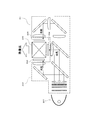
- FIG. 2 is a diagram showing a configuration of the optical engine 20.
- the optical engine 20 includes a lamp 201, a light guide optical system 202, three transmissive liquid crystal panels 203, 204, and 205, and a dichroic prism 206. Note that polarizing plates (not shown) are arranged on the incident side and the emission side of the liquid crystal panels 203, 204, and 205.
- the lamp 201 is, for example, a metal halide lamp or a xenon lamp.
- White light emitted from the lamp 201 is converted into light in the red wavelength band (hereinafter referred to as “R light”), light in the green wavelength band (hereinafter referred to as “G light”), and blue wavelength by the light guide optical system 202.
- the light is separated into band light (hereinafter referred to as “B light”) and applied to the liquid crystal panels 203, 204, and 205.
- the R light, G light, and B light modulated by the liquid crystal panels 203, 204, and 205 are color-combined by the dichroic prism 206 and emitted as video light.
- the light modulation element constituting the optical engine 20 a reflection type liquid crystal panel or a MEMS device can be used in addition to the transmission type liquid crystal panels 203, 204, and 205.
- the optical engine 20 may be configured by a single plate type optical system using one light modulation element and a color wheel, for example, instead of the three plate type optical system including the three light modulation elements as described above. it can.
- an inner cover 40 that covers the air inlet 103 from the inside is mounted in the cabinet 10.
- a cleaning mechanism 50 (shown in FIGS. 3 and 4) is disposed inside the inner cover 40.
- FIG. 3 and 4 are diagrams showing the configuration of the inner cover 40 and the cleaning mechanism 50.
- FIG. FIG. 3 is a perspective view of the inner cover 40 and the cleaning mechanism 50 before the inner cover 40 is attached to the bottom surface of the cabinet 10.
- FIG. 4A is a vertical cross-sectional view along the left-right direction viewed from the front in a state where the inner cover 40 is mounted on the cabinet 10.
- 4B is a longitudinal sectional view along the front-rear direction viewed from the right side in a state where the inner cover 40 is attached to the cabinet 10.
- FIG. 3 is a perspective view of the inner cover 40 and the cleaning mechanism 50 before the inner cover 40 is attached to the bottom surface of the cabinet 10.
- FIG. 4A is a vertical cross-sectional view along the left-right direction viewed from the front in a state where the inner cover 40 is mounted on the cabinet 10.
- 4B is a longitudinal sectional view along the front-rear direction viewed from the right side in a state where the inner cover 40 is attached to the cabinet 10.
- an intake port 401 is formed on the upper surface of the inner cover 40.
- a filter 402 is detachably attached to the back side of the upper surface of the inner cover 40 so as to cover the intake port 401.
- the filter 402 is configured, for example, by knitting resin yarns in a mesh shape.
- the filter 402 may be made of urethane or non-woven fabric.
- the inner cover 40 is fixed to the bottom surface of the cabinet 10 by screwing the mounting portions 403 provided at the four corners thereof to bosses (not shown) provided on the bottom surface of the cabinet 10.
- a cleaning mechanism 50 is provided inside the inner cover 40.
- the cleaning mechanism 50 includes a cylindrical rotating brush 501.
- the rotating brush 501 is rotatably supported by a shaft 503 in the dust box 502.
- An opening 502a is formed on the upper surface of the dust box 502, and a part of the rotating brush 501 is exposed upward from the opening 502a.
- guide pieces 502b are formed on the upper surface of the dust box 502 so as to protrude from both the front and rear sides of the opening 502a.
- Gears 504 and 505 are attached to the front end portion and the rear end portion of the shaft 503 protruding from the dust box 502, respectively.
- the rear end of the shaft 503 is connected to the motor 506.
- the motor 506 is fixed to a mounting plate 502c extending rearward from the upper surface of the dust box 502 by a mounting bracket (not shown).
- a DC motor is used as the motor 506.
- Racks 507 and 508 are disposed in front of and behind the air inlet 103 along the left-right direction, and gears 504 and 505 are engaged with the racks 507 and 508, respectively.
- the inner cover 40 is formed with two guide grooves 404 along the left-right direction with the filter 402 interposed therebetween, and the inner cover 40 is attached to the cabinet 10. Then, the guide piece 502b is inserted into the guide groove 404.
- the motor 506 is driven to rotate in the forward direction and the shaft 503 rotates counterclockwise in FIG. It moves to the left with the dust box 502 while rotating clockwise.
- the motor 506 is driven so as to reverse, and the shaft 503 rotates in the clockwise direction of FIG.
- the brush tip (circumferential surface) of the rotating brush 501 is configured to come into contact with the intake surface 402a of the filter 402.
- a power line (not shown) for energizing the motor 506 is connected to the motor 506 in such a configuration that the motor 506 can move to the left and right.
- FIG. 5 is a block diagram showing the configuration of the projector.
- the projector includes three cooling fans, a panel cooling fan 61, a lamp cooling fan 62, and a power supply cooling fan 63, an exhaust fan 64, a clogging sensor 70, a control circuit unit 80, and a power supply unit. 90.
- the panel cooling fan 61 is disposed in a fan casing (not shown) connected to the intake port 401 of the inner cover 401, and the air taken in from the intake port 401 is placed near the liquid crystal panels 203, 204, 205.
- the liquid crystal panels 203, 204, and 205 are cooled by being ejected from a blower outlet (not shown) disposed in the screen.
- the lamp cooling fan 62 takes in the air after cooling the liquid crystal panels 203, 204, and 205 and supplies the air to the lamp 201 to cool the lamp 201.
- the power supply cooling fan 63 takes in air after cooling the liquid crystal panels 203, 204, and 205 and supplies the air to the power supply unit 90 to cool the power supply unit 90.
- a dedicated inlet for each of the fans 62 and 63 may be formed in the vicinity of the lamp cooling fan 62 and the power supply cooling fan 63, respectively.
- a dedicated inlet is provided together with air from the liquid crystal panels 203, 204, and 205 side. Outside air from the intake port is taken into the fans 62 and 63 and supplied to the lamp 201 and the power supply unit 90.
- the exhaust fan 64 is disposed in the vicinity of the exhaust port 104, takes in warm air that cools the liquid crystal panels 203, 204, 205, the lamp 201, the power supply unit 90, and the like, and discharges it from the exhaust port 104 to the outside of the machine. To do.
- the clogging sensor 70 outputs a clogging signal corresponding to the degree of clogging of the filter 402 to the control unit 810 of the control circuit unit 80.
- the clogging sensor 70 is constituted by an air volume sensor, for example.
- the air volume sensor is disposed on the downstream side of the intake port 401, for example. In this case, when the clogging of the filter 402 proceeds, the amount of air passing through the intake port 401 decreases. From the air volume sensor, a detection voltage corresponding to the air volume is output as a clogging detection signal.
- the control circuit unit 80 includes a control unit 810, a storage unit 820, a key input unit 830, a video signal input unit 840, a video signal processing unit 850, a panel drive unit 860, a fan drive unit 870, a lamp drive unit 880, and a motor drive unit 890. It has.
- the key input unit 830 outputs an input signal corresponding to the button operation of the operation unit (not shown) to the control unit 810.
- the video signal input unit 840 has various input terminals corresponding to various video signals such as an RBG signal and a composite signal, and outputs an externally input video signal to the video signal processing unit 850.
- the video signal processing unit 850 converts the video signal input from the video signal input unit 840 into an RGB video signal that can be displayed on the liquid crystal panels 203, 204, and 205 and outputs the RGB video signal to the panel drive unit 860.
- Panel drive unit 860 drives liquid crystal panels 203, 204, and 205 in accordance with the input video signal and the control signal from control unit 810.
- the fan drive unit 870 drives the panel cooling fan 61, the lamp cooling fan 62, the power supply cooling fan 63, and the exhaust fan 64 in accordance with a control signal from the control unit 810.
- the lamp driving unit 880 drives the lamp 201 in accordance with a control signal from the control unit 810.
- the motor driving unit 890 drives the motor 506 in accordance with a control signal from the control unit 810.
- the storage unit 820 includes a RAM, a ROM, and the like.
- the storage unit 820 stores a control program for giving the control unit 810 a control function.
- the control unit 810 includes a CPU and controls each unit according to the control program.
- the power supply unit 90 supplies power to each unit of the control circuit unit 80.
- each cooling fan 61, 62, 63 is driven, and intake into the cabinet 10 is started.
- the degree of clogging of the filter 402 is detected.
- the motor 506 is driven by the motor driving unit 890.
- the rotating brush 501 operates and the filter 402 is automatically cleaned.
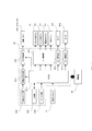
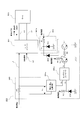
- FIG. 6 is a circuit block diagram showing the configuration of the motor drive unit 890.
- the motor drive unit 890 includes a motor driver 891, a first reference voltage generation circuit 892, and a protection circuit 893.
- the motor driver 891 is composed of an integrated circuit (IC: Integrate Circuit). A power supply voltage is supplied from the power supply unit 90 to the motor driver 891 through the power supply line L1. Further, a control signal for causing the motor 506 to rotate forward, reverse, and stop is input from the control unit 810 via the signal line L2.
- IC Integrate Circuit
- the motor driver 891 has an input port 891a to which the reference voltage Vs is input.
- the motor driver 891 When a control signal for instructing normal rotation or inversion is input from the control unit 810, the motor driver 891 generates a drive voltage based on the reference voltage Vs, for example, equal to the reference voltage Vs or a predetermined voltage with respect to the reference voltage Vs. A drive voltage that is a multiple is generated, and the generated drive voltage is supplied to the motor 506 via the output lines L3 and L4.
- the motor driver 891 is configured so that a drive voltage equal to the reference voltage Vs is generated.
- the first reference voltage generation circuit 892 includes a resistor R1 and a Zener diode ZD1. As the Zener diode ZD1, a Zener diode whose Zener voltage becomes the first reference voltage V1 (for example, 12V) is used. The first reference voltage generation circuit 892 generates the first reference voltage V1 from the power supply voltage by the action of the Zener diode ZD1.
- the motor driver 891 When the motor 506 is in a steady operation state, the first reference voltage V1 generated by the first reference voltage generation circuit 892 is input to the input port 891a of the motor driver 891. As a result, the motor driver 891 outputs a drive voltage having the same magnitude as the first reference voltage V1.
- the current input to the motor driver 891 includes a current for operating the motor driver 891 itself (hereinafter referred to as “driver operating current”).
- the driver operating current varies depending on the type of the motor driver 891.
- the current flowing to the motor driver 891 is larger than the current flowing to the motor 506 by the amount corresponding to the driver operating current.
- the protection circuit 893 includes a resistor R2, a differential amplifier circuit 894, a comparator 895, a Zener diode ZD2, an NPN transistor Tr1, and a Zener diode ZD3.
- the resistor R2 is arranged on the power supply line L1.
- a voltage (terminal voltage) Va corresponding to the magnitude of the current flowing to the motor driver 891 is taken out between the terminals of the resistor R2.
- a resistor R2 having a small resistance value is used in order to suppress a decrease in power supply voltage supplied to the motor driver 891. For this reason, the terminal voltage Va taken out between the terminals of the resistor R2 is small. Therefore, the extracted terminal voltage Va is input to the differential amplifier circuit 894.
- the differential amplifier circuit 894 amplifies the input terminal voltage Va and outputs the amplified terminal voltage Vb to the comparator 895.
- the comparator 895 compares the input terminal voltage Vb with the upper limit voltage Vc generated by the Zener diode ZD2. A current flows through the Zener diode ZD2 via the resistor R3. As the Zener diode ZD2, a Zener diode whose Zener voltage becomes the upper limit voltage Vc is used.
- the upper limit voltage Vc is set to a voltage value of the terminal voltage Vb that appears when the current flowing through the motor 506 becomes a predetermined upper limit current Ilim (see FIG. 7).
- the comparator 895 When the terminal voltage Vb is equal to or lower than the upper limit voltage Vc, the comparator 895 has the output voltage Vd at a low level, and when the terminal voltage Vb exceeds the upper limit voltage Vc, the output voltage Vd is at a high level.
- the high-level output voltage Vd output from the comparator 895 is a switching signal for switching the reference voltage Vs.
- the base of the transistor Tr1 is connected to the comparator 895, and the emitter is grounded.
- a Zener diode ZD3 is disposed between the transistor Tr1 and the resistor R1 of the first reference voltage generation circuit 892.
- a Zener diode ZD3 whose Zener voltage is a second reference voltage V2 (for example, 4V) lower than the first reference voltage V1 is used.
- the Zener diode ZD3 forms a second reference voltage generation unit together with the resistor R1, and the second reference voltage V2 is generated from the power supply voltage by the action of the Zener diode ZD3.
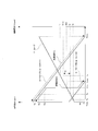
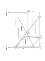
- FIG. 7 is a diagram showing the relationship between the rotational speed N and the output torque T (NT curve) and the relationship between the output torque T and the drive current I (TI curve) in the motor 506.
- an NT curve A and an NT curve B are NT curves when the reference voltage Vs input to the motor driver 891 is the first reference voltage V1 and the second reference voltage V2, respectively.
- the rotational speed N decreases as the load applied from the outside increases, and the output torque T increases accordingly. That is, if no load is applied and the rotational speed N is maximum (Nmax), the output torque T is minimum (Tmin). On the other hand, when the load is large and the motor 506 is in a restrained state (locked state) and the rotational speed N becomes zero, the output torque T becomes maximum (Tmax). Further, the motor 506 increases the drive current I flowing through the motor 506 as the output torque T increases.
- the load applied to the motor 506 by cleaning the filter 402 by the rotating brush 501 is not so large. Therefore, during steady operation, the output torque T of the motor 506 changes within a relatively low range (between Tx and Ty in FIG. 7), and the rotational speed is also within a relatively high range (between Nx and Ny in FIG. 7). ).
- the rotational speed N of the motor 506 is greatly decreased, and the output torque T can be significantly increased accordingly.
- the output torque T of the motor 506 may exceed a dangerous torque Tz that may cause damage between the shaft 503 and the gears 504 and 505 or between the gears 504 and 505 and the racks 507 and 508. is there.
- the protection circuit 893 can suppress the output torque T of the motor 506 from becoming excessive.
- a current range that is smaller than the drive current Iz corresponding to the dangerous torque Tz and larger than the drive current Iy corresponding to the critical output torque Ty during steady operation, particularly the maximum torque Tmax in the NT curve B.
- the upper limit current Ilim is set in a current range W that is smaller than the drive current Imax corresponding to and greater than the drive current Iy. Then, as described above, the upper limit voltage Vc of the comparator 895 is set based on the upper limit current Ilim.
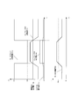
- FIG. 8 is a timing chart showing a voltage state in each part of the protection circuit 893 when the driving current I of the motor 506 fluctuates.
- the drive current I of the motor 506 increases.
- the drive current I exceeds the upper limit current Ilim
- the amplified terminal voltage Vb exceeds the upper limit voltage Vc
- the output voltage Vd of the comparator 895 becomes high level.
- the transistor Tr1 is turned on, and a current flows through the Zener diode ZD3.
- the reference voltage Vs input to the motor driver 891 is switched to the second reference voltage V2 by the Zener diode ZD3.
- the motor 506 is supplied with a drive voltage based on the second reference voltage V2, here, a drive voltage having the same magnitude as the second reference voltage V2.
- the drive current I becomes smaller than the upper limit current Ilim.
- the amplified terminal voltage Vb becomes equal to or lower than the upper limit voltage Vc, and the output voltage Vd of the comparator 895 becomes low level.
- the transistor Tr1 is turned off and no current flows through the Zener diode ZD3, and the reference voltage Vs input to the motor driver 891 is switched to the first reference voltage V1.
- the drive voltage of the motor 506 is raised, and the rotational speed N of the motor 506 increases to the rotational speed Na according to the NT curve, as shown in FIG.
- the load applied to the motor 506 increases, and accordingly, when the current flowing through the motor 506 increases, The driving voltage is reduced. Thereby, even if the motor 506 becomes a restraint state after that, it can prevent that the output torque T of the motor 506 becomes excessive. Therefore, it is possible to prevent problems caused by excessive output torque T in the motor 506, such as damage between the shaft 503 and the gears 504 and 505 and between the gears 504 and 505 and the racks 507 and 508.
- the motor 506 can be protected even if it is a simple DC motor that does not have a function of outputting a pulse signal corresponding to the rotation.
- the upper limit current Ilim can also be set to a range W0 between the drive current Imax and the drive current Iz.
- the driving current I of the motor 506 exceeds the upper limit current Ilim and the reference voltage Vs is switched from the first reference voltage V1 to the second reference voltage V2, the driving is performed.
- the motor 506 is immediately put into a restrained state.
- the drive current I becomes the drive current Imax corresponding to the maximum torque Tmax. Since the drive current Imax is smaller than the upper limit current Ilim, the reference voltage Vs is immediately switched from the second reference voltage V2 to the first reference voltage V1, and the drive voltage is raised.
- the drive current I immediately exceeds the upper limit current Ilim again, so that the first reference voltage V1 is switched to the second reference voltage V2.
- the upper limit current Ilim is set to a range W0 between the drive current Imax and the drive current Iz, the drive voltage to the motor 506 can be in a state where it frequently repeats vertical movement.
- the upper limit current Ilim is set in the current range W that is smaller than the drive current Imax and larger than the drive current Iy. Therefore, the reference voltage Vs is not frequently switched as described above, and it is possible to prevent a situation in which the drive voltage frequently fluctuates up and down.
- the driving of the motor 506 is continued without stopping. Therefore, it is possible to remove as much as possible the factor that increased the load applied to the motor 506. For example, if the foreign matter adhering to the filter 402 is removed by continuously operating the rotary brush 501, the motor 506 returns to the steady operation again, and then the steady operation of the motor 506 can be continued.
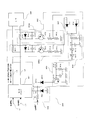
- FIG. 10 is a circuit block diagram illustrating a configuration of a motor driving unit 890 according to a modified example.
- the configuration of the protection circuit 893 is different from that of the above embodiment.
- the configurations of the motor driver 891 and the first reference voltage generation circuit 892 are the same as those in the above embodiment.
- the current flowing through the motor driver 891 is taken out as the current flowing through the motor 506.
- the current flowing through the motor 506 is directly taken out.
- the protection circuit 893 includes a first switching signal generation unit 896a, a second switching signal generation unit 896b, a signal synthesis unit 897, a signal shaping unit 898, and a reference voltage switching unit 899.
- the first switching signal generator 896a includes resistors R11, R12, and R13, a PNP transistor Tr11, a diode D11, and a capacitor C11.
- the resistor R11 is arranged on the output line L3, and takes out a voltage (terminal voltage) corresponding to the current flowing from the motor driver 891 to the motor 506 when the motor 506 is rotating forward.
- the terminal voltage of the resistor R11 is input between the base and emitter of the transistor Tr11.
- the collector of the transistor Tr11 is grounded via resistors R12 and R13.
- a diode D11 and a capacitor C11 are arranged between the terminals of the resistor R11.
- the diode D11 bypasses the current that is about to flow to the resistor R1 when the motor 506 is reversed. Thereby, the voltage drop by resistance R11 can be suppressed and it can suppress that the electric current which flows into the motor 506 falls by voltage drop. Further, since the terminal voltage of the resistor R11 generated at the time of inversion is suppressed, the transistor Tr11 can be protected.
- the capacitor C11 removes noise applied to the first switching signal generation unit 896a, such as spike noise generated from the motor 506.
- the second switching signal generation unit 896b includes resistors R14, R15, R16, a PNP transistor Tr12, a diode D12, and a capacitor C12.
- the configuration of the second switching signal generation unit 896b is the same as that of the first switching signal generation unit 896a.
- the resistor R14 is arranged on the output line L4, and extracts a voltage (terminal voltage) corresponding to the current flowing from the motor driver 891 to the motor 506 when the motor 506 is reversed.
- the signal synthesis unit 897 includes two diodes D13 and D14. A switching signal is input from the first switching signal generation unit 896a to the anode of the diode D13, and a switching signal is input from the second switching signal generation unit 896b to the anode of the diode D14. When a switching signal is input from one of the first switching signal generation unit 896a and the second switching signal generation unit 896b, the signal synthesis unit 897 outputs the input switching signal to the signal shaping unit 898.
- the signal shaping unit 898 includes Schmitt trigger inverters IC11 and IC12, a resistor R17, and a capacitor C13.
- the signal shaping unit 898 removes noise included in the input switching signal, amplifies the switching signal, and outputs the amplified signal to the reference voltage switching unit 899.
- the reference voltage switching unit 899 includes an NPN transistor Tr13, resistors R18 and R19, and a capacitor C14. When a switching signal is input to the reference voltage switching unit 899, the transistor Tr13 is turned on.
- Zener diode ZD11 is arranged between resistor R1 and the collector of transistor Tr13.
- a Zener diode whose Zener voltage is the second reference voltage V2 is used as in the Zener diode ZD3.
- the transistor Tr13 is turned on by the switching signal, a current flows through the Zener diode ZD11, and the reference voltage Vs input to the motor driver 891 is switched from the first reference voltage V1 to the second reference voltage V2.
- the protection circuit 893 can also be configured to directly extract the current flowing through the motor 506.
- each of the current that flows when the motor 506 rotates in the forward direction and the current that flows when the motor 506 reverses is converted into a voltage.
- two of the first switching signal generation unit 896a and the second switching signal generation unit 896b are necessary.
- the protection circuit 893 is configured to extract the current that flows to the motor driver 891 as in the above embodiment, it is necessary to extract each of the current that flows when the motor 506 rotates in the forward direction and the current that flows when the motor 506 reverses. There is no need to provide a corresponding circuit configuration.
- the differential amplifier circuit 894 and the comparator 895 are used for the protection circuit 893.
- a known current-voltage conversion circuit 894a obtained by applying a constant current circuit using an operational amplifier may be used.
- the differential amplifier circuit 894 In the differential amplifier circuit 894, variation in the magnitude of the offset voltage becomes large depending on the accuracy of the resistors constituting the differential amplifier circuit 894. Therefore, when the differential amplifier circuit 894 is used, if the variation in the offset voltage cannot be ignored, it may be necessary to perform resistance adjustment using a semi-fixed resistor or the like. On the other hand, the current-voltage conversion circuit 894 can suppress variations in the offset voltage due to the accuracy of the resistance as compared with the differential amplifier circuit 894 described above. For this reason, if the current-voltage conversion circuit 894a is used, it is possible to suppress the variation in the offset voltage and to eliminate the resistance adjustment work by allowing the variation.
- a hysteresis comparator 895a may be used instead of the comparator 895.
- the current flowing through the motor driver 891 includes the driver operating current used for the operation of the motor driver 891 itself.
- the driver operating current may be greatly reduced. Due to this influence, the current to the motor driver 891 may be reduced.
- the output of the comparator 895 may immediately switch from the high level to the low level. That is, if the current flowing through the resistor R2 fluctuates due to fluctuations in the driver operating current of the motor driver 891, the output of the comparator 895 may be frequently switched. In this case, the reference voltage is frequently switched, and the operation of the protection circuit 893 becomes unstable.
- the hysteresis comparator 895a if the hysteresis comparator 895a is used, even if the current flowing through the resistor R2 fluctuates, the output of the hysteresis comparator 895a does not frequently switch because the upper limit voltage Vc has a predetermined hysteresis. For this reason, the reference voltage is not frequently switched, and the operation of the protection circuit 893 is stabilized.
- the output of the hysteresis comparator 895a becomes low level when the terminal voltage Vb exceeds the upper limit voltage Vc. Therefore, a NOT circuit including the transistor Tr2 and the resistors R4 and R5 is provided between the hysteresis comparator 895a and the transistor Tr1. With this NOT circuit, the transistor Tr1 can be turned on when the output of the hysteresis comparator 895a becomes a low level.
- the protection circuit 893 may be one using a current-voltage conversion circuit 894a and a comparator 895, or may be one using a differential amplifier circuit 894 and a hysteresis comparator 895a.
- the current flowing in the motor driver 891 may be monitored by the circuit configuration shown in FIG. 10 similar to the protection circuit 893 of the modified example.
- the resistor R11 of the first switching signal generator 896a is arranged on the power supply line L1.
- the second switching signal generation unit 896b and the signal synthesis unit 897 are removed, and the switching signal output from the first switching signal generation unit 896a is directly input to the signal shaping unit 898.
- the current flowing through the motor 506 may be directly monitored by the circuit configuration shown in FIG. 6 similar to the protection circuit 893 of the above embodiment.
- two sets of circuit configurations each including a resistor R1 and a differential amplifier circuit 894 are provided so as to correspond to the output lines L3 and L4, respectively, and the two differential amplifier circuits 894 and the comparator 895 are connected to each other.
- a signal synthesis unit similar to that of the modification example is provided.
- the signal shaping unit 898 is provided between the signal synthesis unit 897 and the reference voltage switching unit 899.
- the reference voltage switching unit 899 is appropriately set by the switching signal output from the signal synthesis unit 897. If is operated, the signal shaping unit 898 can be removed.
- the motor driving device of the present invention is applied to the motor driving unit 890 for driving the motor 506 of the cleaning mechanism 50.
- the present invention is not limited to this, and the motor drive device of the present invention can also be applied to the fan drive unit 870 that drives the motors of the cooling fans 61, 62, 63 and the exhaust fan 64.
- the projector may include a lens shift mechanism that moves the projection lens 30 up, down, left, and right in order to adjust the vertical and horizontal positions of the projected image.
- the motor constituting the lens shift mechanism is driven by the motor driving unit.
- the motor driving device of the present invention may be applied to this motor driving unit.
- the motor drive device of the present invention is applied to a projector.
- the present invention is not limited to this, and the motor drive device of the present invention may be applied to other electrical devices.
- Rotating brush (driven part) 506 Motor 80 Control circuit section 890 Motor drive section (motor drive apparatus) 891 Motor driver (drive circuit) 891a Input port (input unit) 892 First reference voltage generation circuit (first reference voltage generation unit) 893 Protection circuit (Protection circuit part) R1 resistor (second reference voltage generator) ZD3 Zener diode (second reference voltage generator) R2 resistance (signal output part) 894 Differential amplifier circuit (signal output unit) 895 Comparator (signal output unit) Tr1 transistor (voltage switching part) 896a First switching signal generator (signal output unit) 896b Second switching signal generator (signal output unit) 899 Reference voltage switching unit (voltage switching unit) 90 Power supply
Landscapes
- Engineering & Computer Science (AREA)
- Power Engineering (AREA)
- Control Of Direct Current Motors (AREA)
Abstract
【課題】モータが拘束状態となった際にモータを容易に保護できるモータ駆動装置を提供する。 【解決手段】モータ駆動部890は、基準電圧Vsが入力される入力ポート891aを有し、電源部90から供給された電源電圧から基準電圧Vsに基づく駆動電圧を生成してモータ506へ供給するモータドライバー891と、モータ506に流れる電流の大きさが所定の上限電流レベルを超えると、駆動電圧が小さくなるように基準電圧Vsを切り替える保護回路893とを備える。保護回路部893は、電源部90からモータドライバー891に流れる電流の大きさを、モータ506に流れる電流の大きさとして取り出す。
Description
本発明は、モータを駆動するモータ駆動装置に関する。また、本発明は、モータ駆動装置を備える投写型表示装置に関する。
従来、モータによって各種の被駆動部が駆動される。たとえば、発熱部品を冷却するためのファンやフィルタを掃除するための回転ブラシなどがモータによって駆動される。この場合、予期せぬ異物などが原因となって、モータが拘束される場合がある。モータが拘束され、その回転数が大きく低下すると、モータに流れる電流が大きく上昇するとともに、モータの出力トルクが大きく上昇する。こうなると、モータと被駆動部との連結部分が破損する虞がある。また、モータが、ギア等の伝達部材を介して被駆動部と連結されている場合には、連結部材が破損する虞がある。
そこで、モータを駆動するモータ駆動回路に保護回路が備えられ得る。たとえば、保護回路は、回転時にモータから出力されるパルス信号を検出することにより、モータが拘束状態となったか否かを判断するよう構成される。そして、保護回路は、モータが拘束状態になったと判断すると、モータに流れる電流を低減させる(特許文献1参照)。
しかしながら、上記の保護回路は、パルス信号を出力する機能を有しないモータを駆動するモータ駆動回路には用いることができない。
本発明は、かかる課題に鑑みてなされたものであり、モータが拘束状態となった際にモータを容易に保護できるモータ駆動装置および投写型表示装置を提供することを目的とする。
本発明の第1の態様は、モータを駆動するモータ駆動装置に関する。本態様に係るモータ駆動装置は、基準電圧が入力される入力部を有し、電源部から供給された電源電圧から前記基準電圧に基づく駆動電圧を生成して前記モータへ供給する駆動回路部と、前記モータに流れる電流の大きさが所定の上限電流レベルを超えると、前記駆動電圧が小さくなるように前記基準電圧を切り替える保護回路部とを備える。
本発明の第1の態様に係るモータ駆動装置によれば、モータに加わる負荷が大きくなることにより、モータに流れる電流が上昇すると、モータへの駆動電圧が小さくされる。これにより、モータが拘束状態となった際のモータの出力トルクの上昇が抑えられる。
第1の態様に係るモータ駆動装置において、前記保護回路部は、前記電源部から前記駆動回路部に流れる電流の大きさを、前記モータに流れる電流の大きさとして取り出すような構成とされ得る。
このような構成とすれば、モータを正転および反転させる構成とした場合に、電源部から駆動回路部へ流れる電流の方向は、正転時と反転時とで同じである。よって、駆動回路部からモータに流れる電流の大きさを取り出す場合と違って、正転時と反転時に流れる電流の方向に対応して、それぞれの方向ごとに、電流を取り出すための回路構成を設ける必要がない。
より具体的な構成として、たとえば、第1の態様に係るモータ駆動装置は、前記入力部に入力される第1基準電圧を生成する第1基準電圧生成部を備えるような構成とされ得る。さらに、前記保護回路は、前記第1基準電圧よりも低い第2基準電圧を生成する第2基準電圧生成部と、前記モータに流れる電流が前記上限電流レベルを超えると、前記基準電圧を切り替えるための切替信号を出力する信号出力部と、前記信号出力部から前記切替信号が出力されると、前記基準電圧を、前記第1基準電圧から前記第2基準電圧へ切り替える電圧切替部とを含むような構成とされ得る。
また、前記信号出力部は、前記モータに流れる電流の大きさを電圧の大きさとして取り出し、取り出された電圧が前記上限電流レベルに対応する上限電圧レベルを超えると、前記基準電圧を切り替えるための切替信号を出力するような構成とされ得る。
さらに、前記信号出力部は、前記電源部から前記駆動回路部へ電流を供給する電源ラインに配された抵抗を含み、当該抵抗の端子電圧を取り出すような構成とされ得る。
第1の態様に係るモータ駆動装置において、前記上限電流レベルが、前記第2基準電圧に基づく前記駆動電圧が供給された状態で前記モータの回転が外力により拘束されて停止状態となったときに前記モータに流れる電流レベルよりも低くなるよう、前記上限電圧レベルが設定され得る。
このような構成とすれば、基準電圧が頻繁に切り替わることによって駆動電圧が頻繁に上下に変動するような状態が起こるのを防止することができる。
本発明の第2の態様は、投写型表示装置に関する。本態様に係る投写型表示装置は、被駆動部に連結されたモータと、前記モータを駆動する、第1の態様に係るモータ駆動装置とを備える。
本発明の第2の態様に係る投写型表示装置によれば、第1の態様に係るモータ駆動装置を備えることにより、モータが拘束状態となった際のモータの出力トルクの上昇が抑えられる。
たとえば、投写型表示装置には、光学部品を冷却するため、内部に外気が導入するための吸気口が設けられ、吸気口にはフィルタが配される。さらに、投写型表示装置には、フィルタに付着した不要物を除去するため、回転ブラシを有する除去装置が配される。この場合、回転ブラシが被駆動部としてモータに連結され得る。
以上のとおり、本発明によれば、モータが拘束状態となった際にモータを容易に保護できるモータ駆動装置および投写型表示装置を提供することができる。
本発明の効果ないし意義は、以下に示す実施の形態の説明により更に明らかとなろう。ただし、以下の実施の形態は、あくまでも、本発明を実施化する際の一つの例示であって、本発明は、以下の実施の形態に記載されたものに何ら制限されるものではない。
以下、図面を参照して、本発明の実施の形態について説明する。
図1は、プロジェクタの構成を示す外観斜視図である。図1(a)は、プロジェクタを斜め上方から見た斜視図であり、図1(b)は、プロジェクタを上下逆さまにして斜め上方から見た斜視図である。
図1を参照して、プロジェクタは、横長の略直方体形状を有するキャビネット10を備えている。キャビネット10には、前面中央に投写窓101が形成されている。また、キャビネット10の底面には、四隅に脚部102が設けられているとともに、左側面寄りの位置に、多数の孔からなる吸気口103が形成されている。さらに、キャビネット10の右側面には、多数の孔からなる排気口104が形成されている。
キャビネット10の内部には、光学エンジン20および投写レンズ30が配されている。光学エンジン20は、ランプからの光を映像信号に基づいて変調することにより映像光を生成する。光学エンジン20には、投写レンズ30が装着されており、投写レンズ30の前端部が、投写窓101から前方に露出している。投写レンズ30は、光学エンジン20で生成された映像光を、プロジェクタの前方に配されたスクリーンに拡大投写する。
図2は、光学エンジン20の構成を示す図である。
図2に示すように、光学エンジン20は、ランプ201と、導光光学系202と、3つの透過型の液晶パネル203、204、205と、ダイクロイックプリズム206とを備えている。なお、液晶パネル203、204、205の入射側と出射側には図示しない偏光板が配されている。
ランプ201は、たとえば、メタルハライドランプやキセノンランプである。ランプ201から出射された白色光は、導光光学系202によって赤色波長帯の光(以下、「R光」という)と、緑色波長帯の光(以下、「G光」という)と、青色波長帯の光(以下、「B光」という)に分離され、液晶パネル203、204、205に照射される。これら液晶パネル203、204、205によって変調されたR光、G光、B光は、ダイクロイックプリズム206によって色合成され、映像光として出射される。
なお、光学エンジン20を構成する光変調素子としては、上記透過型の液晶パネル203、204、205の他、反射型の液晶パネルや、MEMSデバイスを用いることもできる。また、光学エンジン20は、上記のように3つの光変調素子を備えた3板式の光学系ではなく、たとえば、1つの光変調素子とカラーホイールを用いた単板式の光学系により構成することもできる。
図1に戻り、キャビネット10内には、内側から吸気口103を覆う内カバー40が装着されている。内カバー40の内部には、清掃機構50(図3、図4に図示)が配置されている。
図3および図4は、内カバー40および清掃機構50の構成を示す図である。図3は、内カバー40がキャビネット10の底面に装着される前の内カバー40および清掃機構50の斜視図である。図4(a)は、内カバー40がキャビネット10に装着された状態での、前方から見た左右方向に沿う縦断面図である。また、図4(b)は、内カバー40がキャビネット10に装着された状態での、右方から見た前後方向に沿う縦断面図である。
図3および図4を参照して、内カバー40の上面には、取込口401が形成されている。また、内カバー40の上面裏側には、取込口401を覆うように、フィルタ402が取り外し可能に装着されている。フィルタ402は、たとえば、樹脂製の糸をメッシュ状に編むことにより構成されている。この他、フィルタ402は、ウレタンや不織布によって構成されても良い。内カバー40は、その四隅に設けられた取付部403が、キャビネット10の底面に設けられたボス部(図示せず)にネジ止されることにより、キャビネット10の底面に固定される。
後述する各冷却ファンが回転すると、図4(a)に示すように、吸気口103から外気が取り込まれる。取り込まれた空気は、フィルタ402を通って取込口401からキャビネット10内に流入する。このとき、空気中に含まれた埃や塵は、フィルタ402を通過できず、フィルタ402の吸気面402aに付着する。
フィルタ402の吸気面402aに付着した埃を除去するため、内カバー40の内部には、清掃機構50が設けられている。
清掃機構50は、円筒状の回転ブラシ501を備えている。回転ブラシ501は、ダストボックス502内において、シャフト503によって回転自在に支持されている。ダストボックス502には、上面に開口502aが形成されており、この開口502aから回転ブラシ501の一部が上方に露出している。また、ダストボックス502の上面には、開口502aの前後両側にガイド片502bが突出形成されている。
ダストボックス502から突き出たシャフト503の前端部および後端部には、それぞれ、ギア504、505が取り付けられている。シャフト503の後端は、モータ506に連結されている。モータ506は、ダストボックス502の上面から後方に延び出した取付板502cに、図示しない取付金具によって固定される。モータ506には、直流モータが用いられている。
吸気口103の前方および後方には、左右方向に沿ってラック507、508が配置されており、ギア504、505が、それぞれ、ラック507、508に係合している。また、図4(b)に示すように、内カバー40には、フィルタ402を挟んで、2つのガイド溝404が左右方向に沿って形成されており、内カバー40がキャビネット10に装着されると、ガイド片502bがガイド溝404に挿入される。
こうして、回転ブラシ501がラック507、508の右端にある状態において、モータ506が正転するように駆動され、シャフト503が図4(a)の反時計方向に回転すると、回転ブラシ501が、反時計方向に回転しながら、ダストボックス502とともに左方向に移動する。また、回転ブラシ501がラック507、508の左端に到達すると、モータ506が反転するように駆動され、シャフト503が図4(a)の時計方向に回転する。これにより、回転ブラシ501が、時計方向に回転しながら、ダストボックス502とともに右方向に移動する。回転ブラシ501のブラシ先端(周面)は、フィルタ402の吸気面402aに接触するよう構成されており、回転ブラシ501が左右方向に往復運動すると、ブラシ先端でフィルタ402に付着した埃が掻き落される。掻き落された埃は、図4(a)の一点鎖線の矢印に示す如く、ダストボックス502内に収容され、その底部に溜められる。
なお、モータ506へ通電するための電力線(図示せず)は、モータ506ともに左右に移動できるような構成にて、モータ506に接続されている。
図5は、プロジェクタの構成を示すブロック図である。
プロジェクタは、上述した構成に加えて、パネル冷却ファン61、ランプ冷却ファン62および電源冷却ファン63の3つの冷却ファンと、排気ファン64と、目詰まりセンサ70と、制御回路部80と、電源部90とを備えている。
パネル冷却ファン61は、内カバー401の取込口401に連結されたファンケーシング(図示せず)内に配置されおり、取込口401から取り込んだ空気を、液晶パネル203、204、205の近傍に配された吹出口(図示せず)から噴出させ、液晶パネル203、204、205を冷却する。
ランプ冷却ファン62は、液晶パネル203、204、205を冷却した後の空気を取り込み、ランプ201へ供給してランプ201を冷却する。電源冷却ファン63は、液晶パネル203、204、205を冷却した後の空気を取り込み、電源部90へ供給して電源部90を冷却する。
なお、ランプ冷却ファン62および電源冷却ファン63の近傍に、それぞれ、各ファン62、63専用の吸気口が形成されても良く、この場合、液晶パネル203、204、205側からの空気とともに専用の吸気口からの外気が各ファン62、63に取り込まれ、ランプ201や電源部90に供給される。
排気ファン64は、排気口104の近傍に配されており、液晶パネル203、204、205、ランプ201、電源部90等を冷却して温まった空気を取り込んで、排気口104から機外へ排出する。
目詰まりセンサ70は、フィルタ402の目詰まり具合に応じた目詰まり信号を制御回路部80の制御部810に出力する。目詰まりセンサ70は、たとえば、風量センサによって構成される。風量センサは、たとえば、取込口401の下流側に配される。この場合、フィルタ402の目詰まりが進行すると、取込口401を通過する風量が低下する。風量センサからは、目詰まり検出信号として、風量に応じた検出電圧が出力される。
制御回路部80は、制御部810、記憶部820、キー入力部830、映像信号入力部840、映像信号処理部850、パネル駆動部860、ファン駆動部870、ランプ駆動部880およびモータ駆動部890を備えている。
キー入力部830は、操作部(図示せず)のボタン操作に応じた入力信号を制御部810に出力する。
映像信号入力部840は、RBG信号、コンポジット信号等の各種映像信号に対応する各種入力端子を有し、外部から入力された映像信号を映像信号処理部850へ出力する。映像信号処理部850は、映像信号入力部840から入力された映像信号を液晶パネル203、204、205で表示できるRGBの映像信号に変換してパネル駆動部860に出力する。パネル駆動部860は、入力された映像信号および制御部810からの制御信号に従って液晶パネル203、204、205を駆動する。
ファン駆動部870は、制御部810からの制御信号に従って、パネル冷却ファン61、ランプ冷却ファン62、電源冷却ファン63および排気ファン64を駆動する。ランプ駆動部880は、制御部810からの制御信号に従ってランプ201を駆動する。
モータ駆動部890は、制御部810からの制御信号に従って、モータ506を駆動する。
記憶部820は、RAM、ROM等で構成されている。記憶部820には、制御部810に制御機能を付与するための制御プログラムが記憶されている。制御部810は、CPUを備え、かかる制御プログラムに従って各部を制御する。
電源部90は、制御回路部80の各部に電力を供給する。
プロジェクタの運転が開始されると、各冷却ファン61、62、63が駆動され、キャビネット10内への吸気が開始される。運転中はフィルタ402の目詰まり具合が検出され、フィルタ402が目詰まりを起こすと、モータ駆動部890によりモータ506が駆動される。これにより、回転ブラシ501が動作し、フィルタ402が自動的に掃除される。
図6は、モータ駆動部890の構成を示す回路ブロック図である。
モータ駆動部890は、モータドライバー891と、第1基準電圧生成回路892と、保護回路893とを備えている。
モータドライバー891は、集積回路(IC:Integrate Circuit)で構成されている。モータドライバー891には、電源ラインL1を介して電源部90から電源電圧が供給される。また、信号ラインL2を介して制御部810からモータ506を正転、反転および停止させるための制御信号が入力される。
モータドライバー891は、基準電圧Vsが入力される入力ポート891aを有する。制御部810から正転または反転を指示する制御信号が入力されると、モータドライバー891は、基準電圧Vsに基づく駆動電圧、たとえば、基準電圧Vsと等倍、あるいは基準電圧Vsに対して所定の倍数となる駆動電圧を生成し、生成した駆動電圧を出力ラインL3、L4を介してモータ506に供給する。なお、本実施の形態では、基準電圧Vsと等倍の駆動電圧が生成されるよう、モータドライバー891が構成されている。
第1基準電圧生成回路892は、抵抗R1とツェナーダイオードZD1とを含む。ツェナーダイオードZD1には、ツェナー電圧が第1基準電圧V1(たとえば、12V)となるツェナーダイオードが用いられる。第1基準電圧生成回路892は、ツェナーダイオードZD1の働きにより、電源電圧から第1基準電圧V1を生成する。
モータ506が定常の動作状態ときには、第1基準電圧生成回路892により生成された第1基準電圧V1がモータドライバー891の入力ポート891aに入力される。これにより、モータドライバー891からは第1基準電圧V1と同じ大きさの駆動電圧が出力される。
図6の矢印に示すように、モータドライバー891からは、モータ506が正転する際には出力ラインL3→モータ506→出力ラインL4の順に電流が流れ、モータ506が反転する際には出力ラインL4→モータ506→出力ラインL3の順に電流が流れるように、モータ506へ駆動電圧が供給される。後述するように、モータ506へ流れる電流は、モータ506に加わる負荷の変動により、モータ506の回転数が変動すると、それに伴って変動する。モータ506へ流れる電流が変動すると、それに応じて、電源ラインL1によりモータドライバー891に入力される電流も変動する。
なお、モータドライバー891に入力される電流には、モータドライバー891自身を動作させるための電流(以下、「ドライバー作動電流」という)が含まれる。ドライバー作動電流は、モータドライバー891の種類によって異なる。モータドライバー891へ流れる電流は、ドライバー作動電流に対応する分だけ、モータ506へ流れる電流よりも多くなる。
保護回路893は、抵抗R2と、差動増幅回路894と、コンパレータ895と、ツェナーダイオードZD2と、NPN型のトランジスタTr1と、ツェナーダイオードZD3とを含む。
抵抗R2は、電源ラインL1に配されている。抵抗R2の端子間からは、モータドライバー891へ流れる電流の大きさに応じた電圧(端子電圧)Vaが取り出される。モータドライバー891に供給される電源電圧の低下を抑えるため、抵抗R2は抵抗値の小さなものが用いられる。このため、抵抗R2の端子間から取り出される端子電圧Vaは小さなものとなる。よって、取り出された端子電圧Vaは、差動増幅回路894に入力される。
差動増幅回路894は、入力された端子電圧Vaを増幅し、増幅した端子電圧Vbをコンパレータ895へ出力する。
コンパレータ895は、入力された端子電圧Vbを、ツェナーダイオードZD2により生成される上限電圧Vcと比較する。ツェナーダイオードZD2には、抵抗R3を介して電流が流れる。ツェナーダイオードZD2には、ツェナー電圧が上限電圧Vcとなるツェナーダイオードが用いられる。上限電圧Vcは、モータ506に流れる電流が予め定めた上限電流Ilim(図7参照)となったときに現われる端子電圧Vbの電圧値に設定されている。
コンパレータ895は、端子電圧Vbが上限電圧Vc以下であれば、その出力電圧Vdがローレベルとなり、端子電圧Vbが上限電圧Vcを超えれば、その出力電圧Vdがハイレベルとなる。コンパレータ895から出力されるハイレベルの出力電圧Vdは、基準電圧Vsを切り替えるための切替信号となる。
トランジスタTr1は、ベースがコンパレータ895に接続され、エミッタが接地されている。そして、トランジスタTr1と第1基準電圧生成回路892の抵抗R1との間にツェナーダイオードZD3が配されている。ツェナーダイオードZD3には、ツェナー電圧が第1基準電圧V1よりも低い第2基準電圧V2(たとえば、4V)となるツェナーダイオードが用いられる。ツェナーダイオードZD3は、抵抗R1とともに第2基準電圧生成部を構成し、ツェナーダイオードZD3の働きにより、電源電圧から第2基準電圧V2が生成される。
図7は、モータ506における、回転数Nと出力トルクTとの関係(N-Tカーブ)、および出力トルクTと駆動電流Iとの関係(T-Iカーブ)を示す図である。図中、N-TカーブAおよびN-TカーブBは、それぞれ、モータドライバー891に入力される基準電圧Vsが第1基準電圧V1および第2基準電圧V2の場合のN-Tカーブである。
モータ506は、外部から加わる負荷が大きくなるほど回転数Nが低下し、それに伴って出力トルクTが上昇する。即ち、負荷が全く加わらず、回転数Nが最大(Nmax)であれば出力トルクTが最小(Tmin)となる。一方、負荷が大きくてモータ506が拘束状態(ロック状態)となり、回転数Nがゼロになると、出力トルクTが最大(Tmax)となる。また、モータ506は、出力トルクTが大きくなるほど、モータ506に流れる駆動電流Iが大きくなる。
本実施の形態では、通常の埃等を除去する場合、回転ブラシ501によるフィルタ402の清掃によってモータ506に加わる負荷はそれほど大きくない。よって、定常動作時には、モータ506の出力トルクTは、比較的低い範囲内(図7のTxとTyの間)を推移し、回転数も比較的高い範囲内(図7のNxとNyの間)を推移する。
しかしながら、フィルタ402に除去しにくい異物が付着するなどして、回転ブラシ501に大きな負荷が加わると、モータ506の回転数Nが大きく低下し、それに伴い出力トルクTが大きく上昇し得る。こうなると、モータ506の出力トルクTが、シャフト503とギア504、505との間やギア504、505とラック507、508との間に破損を起こし得るような危険トルクTzを超えてしまう虞がある。本実施の形態では、保護回路893により、モータ506の出力トルクTが過大となるのを抑えることができる。
本実施の形態では、危険トルクTzに対応する駆動電流Izよりも小さく、定常動作時の臨界の出力トルクTyに対応する駆動電流Iyより大きな電流範囲、特に、N-TカーブBにおける最大トルクTmaxに対応する駆動電流Imaxよりも小さく、駆動電流Iyよりも大きな電流範囲Wにおいて、上限電流Ilimが設定される。そして、上述のように、上限電流Ilimに基づいて、コンパレータ895の上限電圧Vcが設定される。
以下、保護回路893の動作にについて説明する。
図8は、モータ506の駆動電流Iが変動したときの保護回路893の各部における電圧の状態を示すタイミングチャートである。
図8を参照して、モータ506が定常動作している場合には、モータ506の駆動電流Iが上限電流Ilimよりも小さくなり、これに応じてモータドライバー891に流れる電流も小さくなるため、抵抗R1の端子電圧Vaが小さくなる。このため、増幅後の端子電圧Vbは上限電圧Vc以下となり、コンパレータ895の出力電圧Vdはローレベルとなる。これにより、トランジスタTr1はオンせず、ツェナーダイオードZD3に電流が流れない。よって、モータドライバー891に入力される基準電圧Vsは、ツェナーダイオードZD1による第1基準電圧V1に維持される。モータ506には、第1基準電圧V1に基づく駆動電圧、ここでは、第1基準電圧V1と同じ大きさの駆動電圧が供給される。
上述したように、回転ブラシ501に過大な負荷が加わることにより、モータ506に加わる負荷が大きくなると、モータ506の駆動電流Iが増加する。駆動電流Iが上限電流Ilimを超えると、増幅後の端子電圧Vbが上限電圧Vcを超え、コンパレータ895の出力電圧Vdがハイレベルとなる。これにより、トランジスタTr1がオンして、ツェナーダイオードZD3に電流が流れる。このとき、ツェナーダイオードZD3に流れる電流が支配的になるため、モータドライバー891に入力される基準電圧Vsは、ツェナーダイオードZD3による第2基準電圧V2に切り替えられる。モータ506には、第2基準電圧V2に基づく駆動電圧、ここでは、第2基準電圧V2と同じ大きさの駆動電圧が供給される。
こうして、駆動電圧が引き下げられると、図7に示すように、モータ506の出力トルクTと駆動電流Iは、上限トルクTlimと上限電流Ilimに維持されたまま、回転数Nが、N-TカーブAに従う回転数NaからN-TカーブBに従う回転数Nbに低下する。その後、上限トルクTlimよりも大きな出力トルクTが必要であれば回転数Nがさらに低下し、必要な出力トルクTと釣り合えば、その出力トルクTに対応する回転数Nでモータ506が回転を継続する。これにより、ゆっくりであるが回転ブラシ501が回転し続ける。
やがて、フィルタ402から異物が除去されることなどにより、モータ506へ加わる負荷が小さくなると、駆動電流Iが上限電流Ilimより小さくなる。すると、増幅後の端子電圧Vbが上限電圧Vc以下となり、コンパレータ895の出力電圧Vdがローレベルとなる。これにより、トランジスタTr1がオフして、ツェナーダイオードZD3に電流が流れなくなり、モータドライバー891に入力される基準電圧Vsが第1基準電圧V1に切り替わる。こうなると、モータ506の駆動電圧が引き上げられ、図7に示すように、モータ506の回転数NがN-Tカーブに従う回転数Naに上昇する。
モータ506へ加わる負荷がかなり大きな場合には、モータ506の回転数Nが、N-TカーブBに従う回転数Nbに低下した後、さらに、回転数Nが低下してゼロとなる。こうして、モータ506が拘束状態になると、モータ506の出力トルクTが最大トルクTmaxとなる。しかしながら、図7に示すように、このときの最大トルクTmaxは、危険トルクTzよりも小さくなる。
このように、本実施の形態では、図7の「保護回路あり」の実線矢印に示すように、モータ506加わる負荷が大きくなり、それに伴って、モータ506に流れる電流が大きくなると、モータ506への駆動電圧が引き下げられる。これにより、その後、モータ506が拘束状態となっても、モータ506の出力トルクTが過大となるのを防止できる。よって、シャフト503とギア504、505との間やギア504、505とラック507、508との間の破損など、モータ506に出力トルクTが過大となることにより不具合が生じるのを防止できる。
なお、図7の「保護回路なし」の破線矢印に示すように、本実施の形態と違って、保護回路893がない場合には、モータ506に加わる負荷が大きくなり、モータ506が拘束状態になると、モータ506の出力トルクTが危険トルクTzを超えてしまう。よって、シャフト503とギア504、505との間やギア504、505とラック507、508との間の破損など、モータ506に出力トルクTが過大となることによる不具合が生じる虞がある。
また、本実施の形態では、モータ506が、回転に応じたパルス信号を出力する機能を有しない単純な直流モータであっても保護することができる。
なお、図9に示すように、上限電流Ilimを、駆動電流Imaxと駆動電流Izとの間の範囲W0に設定することもできる。しかしこの場合、「保護回路あり」の実線矢印に示すように、モータ506の駆動電流Iが上限電流Ilimを超え、基準電圧Vsが第1基準電圧V1から第2基準電圧V2に切り替わると、駆動電圧が引き下げられて、直ちにモータ506が拘束状態となる。これにより、駆動電流Iが最大トルクTmaxに対応する駆動電流Imaxとなる。駆動電流Imaxは、上限電流Ilimよりも小さいため、基準電圧Vsは、直ちに第2基準電圧V2から第1基準電圧V1に切り替わり、駆動電圧が引き上げられる。こうなると、直ちに、再び駆動電流Iが上限電流Ilimを超えるので、第1基準電圧V1から第2基準電圧V2に切り替わる。このように、上限電流Ilimを、駆動電流Imaxと駆動電流Izとの間の範囲W0に設定すると、モータ506への駆動電圧が頻繁に上下動を繰り返す状態になり得る。
本実施の形態では、駆動電流Imaxよりも小さく、駆動電流Iyよりも大きな電流範囲Wにおいて、上限電流Ilimが設定されている。よって、上記のように基準電圧Vsが頻繁に切り替わることがなく、駆動電圧が頻繁に上下に変動するような状態が起こるのを防止することができる。
さらに、本実施の形態では、モータ506の回転数Nが低くなり、あるいはモータ506が拘束状態となっても、モータ506の駆動を停止せずに継続するようにしている。よって、モータ506に加わる負荷が大きくなった要因を、極力取り去ることが可能となる。たとえば、回転ブラシ501が継続して動作されることによってフィルタ402に付着した異物が除去されれば、再びモータ506が定常動作に戻り、その後、モータ506の定常動作を継続させることができる。
<変更例>
図10は、変更例に係るモータ駆動部890の構成を示す回路ブロック図である。本変更例では、保護回路893の構成が上記実施の形態と異なる。モータドライバー891および第1基準電圧生成回路892の構成については、上記実施の形態と同様である。
図10は、変更例に係るモータ駆動部890の構成を示す回路ブロック図である。本変更例では、保護回路893の構成が上記実施の形態と異なる。モータドライバー891および第1基準電圧生成回路892の構成については、上記実施の形態と同様である。
上記実施の形態では、モータドライバー891に流れる電流が、モータ506に流れる電流として取り出される。これに対し、本変更例では、モータ506に流れる電流が直接取り出される。
保護回路893は、第1切替信号生成部896aと、第2切替信号生成部896bと、信号合成部897と、信号整形部898と、基準電圧切替部899とを含む。
第1切替信号生成部896aは、抵抗R11、R12、R13と、PNP型のトランジスタTr11と、ダイオードD11と、コンデンサC11とを含む。
抵抗R11は出力ラインL3に配され、モータ506の正転時にモータドライバー891からモータ506へ流れる電流に応じた電圧(端子電圧)を取り出す。抵抗R11の端子電圧はトランジスタTr11のベース-エミッタ間に入力される。トランジスタTr11のコレクタは抵抗R12、R13を介して接地される。正転時にモータ506に流れる電流が上限電流Ilimを超え、これにより、抵抗R11の端子電圧が、上限電流Ilimに対応する上限電圧を超えると、トランジスタTr11がオンする。これにより、モータ506へ供給される駆動電圧が抵抗R12と抵抗R13とで分圧された電圧が、切替信号として抵抗R12と抵抗R13との間から出力される。
抵抗R11の端子間には、ダイオードD11とコンデンサC11が配されている。ダイオードD11は、モータ506の反転時に抵抗R1に流れようとする電流を迂回させる。これにより、抵抗R11による電圧降下を抑制でき、電圧降下によってモータ506に流れる電流が低下するのを抑制できる。また、反転時に生じる抵抗R11の端子電圧が抑えられるので、トランジスタTr11を保護することができる。
コンデンサC11は、モータ506から発生するスパイクノイズなど、第1切替信号生成部896aに加わるノイズを除去する。
第2切替信号生成部896bは、抵抗R14、R15、R16と、PNP型のトランジスタTr12と、ダイオードD12と、コンデンサC12とを含む。第2切替信号生成部896bの構成は、第1切替信号生成部896aと同様である。抵抗R14は、出力ラインL4に配され、モータ506の反転時にモータドライバー891からモータ506へ流れる電流に応じた電圧(端子電圧)を取り出す。反転時にモータ506に流れる電流が上限電流Ilimを超え、これにより、抵抗R14の端子電圧が、上限電流Ilimに対応する上限電圧を超えると、切替信号が抵抗R15と抵抗R16との間から出力される。
信号合成部897は、2つのダイオードD13、D14含む。ダイオードD13のアノードには、第1切替信号生成部896aから切替信号が入力され、ダイオードD14のアノードには、第2切替信号生成部896bから切替信号が入力される。信号合成部897は、第1切替信号生成部896a、第2切替信号生成部896bの一方から切替信号が入力されると、入力された切替信号を信号整形部898へ出力する。
信号整形部898は、シュミット・トリガー・インバータIC11、IC12と、抵抗R17と、コンデンサC13を含む。信号整形部898は、入力された切替信号に含まれるノイズを除去するとともに切替信号を増幅し、基準電圧切替部899に出力する。
基準電圧切替部899は、NPN型のトランジスタTr13と、抵抗R18、R19と、コンデンサC14を含む。基準電圧切替部899に切替信号が入力されると、トランジスタTr13がオンする。
ツェナーダイオードZD11は、抵抗R1とトランジスタTr13のコレクタとの間に配されている。ツェナーダイオードZD11には、ツェナーダイオードZD3と同様、ツェナー電圧が第2基準電圧V2となるツェナーダイオードが用いられている。切替信号によってトランジスタTr13がオンすると、ツェナーダイオードZD11に電流が流れ、モータドライバー891に入力される基準電圧Vsが、第1基準電圧V1から第2基準電圧V2に切り替えられる。
本変更例のように、保護回路893は、モータ506に流れる電流を直接取り出すような構成とすることもできる。
ただし、本変更例の保護回路893の場合、モータ506の正転時に流れる電流と反転時に流れる電流のそれぞれを、電圧に変換して取り出す回路構成が必要となる。たとえば、本変更例の場合は、第1切替信号生成部896aと第2切替信号生成部896bの2つが必要となる。
これに対し、上記実施の形態のように、保護回路893を、モータドライバー891に流れる電流を取り出すような構成とすれば、モータ506の正転時に流れる電流と反転時に流れる電流のそれぞれを取り出す必要がなく、それぞれ対応する回路構成を設ける必要がない。
<その他>
以上、本実施の形態について説明したが、本発明は上記実施の形態に何ら制限されるものではなく、また、本発明の実施形態も、上記実施の形態に以外に、種々の変更が可能である。
以上、本実施の形態について説明したが、本発明は上記実施の形態に何ら制限されるものではなく、また、本発明の実施形態も、上記実施の形態に以外に、種々の変更が可能である。
たとえば、上記実施の形態では、保護回路893に差動増幅回路894およびコンパレータ895が用いられている。しかしながら、図11に示すように、差動増幅回路894に替えて、オペアンプを用いた定電流回路を応用してなる、既知の電流-電圧変換回路894aを用いても良い。
差動増幅回路894では、差動増幅回路894を構成する抵抗の精度によっては、オフセット電圧の大きさのばらつきが大きくなる。よって、差動増幅回路894を用いた場合、オフセット電圧のばらつきが無視できないときには、半固定抵抗等を用いて抵抗の調整作業を行う必要が生じ得る。一方、電流-電圧変換回路894では、上述の差動増幅回路894に比べて抵抗の精度に起因するオフセット電圧のばらつきを抑制できる。このため、電流-電圧変換回路894aを用いれば、オフセット電圧のばらつきを小さく抑制し、ばらつきを許容することによって抵抗の調整作業を行わなくて済むようにできる。
また、図11に示すように、コンパレータ895に替えて、ヒステリシスコンパレータ895aを用いるようにしても良い。
上述のように、モータドライバー891に流れる電流は、モータドライバー891自身の動作に用いられるドライバー作動電流を含む。モータドライバー891の種類によっては、基準電圧Vsが、第1基準電圧V1から第2基準電圧V2に切り替わると、ドライバー作動電流が大きく減少する場合があり、この影響により、モータドライバー891への電流が低下して、コンパレータ895の出力が直ちにハイレベルからローレベルに切り替わってしまう虞がある。即ち、モータドライバー891のドライバー作動電流の変動によって抵抗R2を流れる電流がゆらぐと、コンパレータ895の出力が頻繁に切り替わる虞
がある。こうなると、基準電圧が頻繁に切り替わってしまい、保護回路893の動作が不安定になってしまう。このような場合、ヒステリシスコンパレータ895aを用いれば、抵抗R2を流れる電流がゆらいでも、上限電圧Vcが所定のヒステリシスを持つため、ヒステリシスコンパレータ895aの出力が、頻繁に切り替わることがない。このため、基準電圧が頻繁に切り替わらず、保護回路893の動作が安定する。
がある。こうなると、基準電圧が頻繁に切り替わってしまい、保護回路893の動作が不安定になってしまう。このような場合、ヒステリシスコンパレータ895aを用いれば、抵抗R2を流れる電流がゆらいでも、上限電圧Vcが所定のヒステリシスを持つため、ヒステリシスコンパレータ895aの出力が、頻繁に切り替わることがない。このため、基準電圧が頻繁に切り替わらず、保護回路893の動作が安定する。
なお、ヒステリシスコンパレータ895aの出力は、コンパレータ895とは逆に、端子電圧Vbが上限電圧Vcを超えるとローレベルとなる。よって、ヒステリシスコンパレータ895aとトランジスタTr1との間には、トランジスタTr2と抵抗R4、R5からなるNOT回路が設けられる。このNOT回路により、ヒステリシスコンパレータ895aの出力がローレベルになったときに、トランジスタTr1をオンさせることができる。
なお、保護回路893は、電流-電圧変換回路894aとコンパレータ895とが用いられたものでも良く、差動増幅回路894とヒステリシスコンパレータ895aとが用いられたものでも良い。
また、上記変更例の保護回路893と同様な図10に記載の回路構成により、モータドライバー891に流れる電流を監視するような構成としても良い。この場合、第1切替信号生成部896aの抵抗R11が、電源ラインL1に配される。第2切替信号生成部896bおよび信号合成部897は取り除かれ、第1切替信号生成部896aから出力された切替信号が、直接、信号整形部898に入力される。
また、上記実施の形態の保護回路893と同様な図6に記載の回路構成により、モータ506に流れる電流を直接監視するような構成としても良い。この場合、出力ラインL3、L4にそれぞれ対応するように、抵抗R1と差動増幅回路894とからなる回路構成が2組設けられ、2つの差動増幅回路894とコンパレータ895との間に、上記変更例と同様な信号合成部が設けられる。
さらに、上記変更例では、信号合成部897と基準電圧切替部899との間に信号整形部898が設けられているが、信号合成部897から出力された切替信号によって適正に基準電圧切替部899が動作するのであれば、信号整形部898を取り除くこともできる。
また、上記実施の形態では、本発明のモータ駆動装置が、清掃機構50のモータ506を駆動するためのモータ駆動部890に適用されている。しかしながら、これに限らず、冷却ファン61、62、63および排気ファン64のそれぞれのモータを駆動するファン駆動部870に、本発明のモータ駆動装置を適用することもできる。さらには、プロジェクタが、投写画像の上下左右の位置を調整するために、投写レンズ30を上下左右に動かすレンズシフト機構を備えても良い。この場合、レンズシフト機構を構成するモータが、モータ駆動部により駆動される。このモータ駆動部に、本発明のモータ駆動装置が適用されても良い。
さらに、上記実施の形態では、本発明のモータ駆動装置を、プロジェクタに適用しているが、これに限らず、本発明のモータ駆動装置を、他の電気機器に適用するようにしてもよい。
この他、本発明の実施の形態は、特許請求の範囲に示された技術的思想の範囲内において、適宜、種々の変更が可能である。
501 回転ブラシ(被駆動部)
506 モータ
80 制御回路部
890 モータ駆動部(モータ駆動装置)
891 モータドライバー(駆動回路部)
891a 入力ポート(入力部)
892 第1基準電圧生成回路(第1基準電圧生成部)
893 保護回路(保護回路部)
R1 抵抗(第2基準電圧生成部)
ZD3 ツェナーダイオード(第2基準電圧生成部)
R2 抵抗(信号出力部)
894 差動増幅回路(信号出力部)
895 コンパレータ(信号出力部)
Tr1 トランジスタ(電圧切替部)
896a 第1切替信号生成部(信号出力部)
896b 第2切替信号生成部(信号出力部)
899 基準電圧切替部(電圧切替部)
90 電源部
506 モータ
80 制御回路部
890 モータ駆動部(モータ駆動装置)
891 モータドライバー(駆動回路部)
891a 入力ポート(入力部)
892 第1基準電圧生成回路(第1基準電圧生成部)
893 保護回路(保護回路部)
R1 抵抗(第2基準電圧生成部)
ZD3 ツェナーダイオード(第2基準電圧生成部)
R2 抵抗(信号出力部)
894 差動増幅回路(信号出力部)
895 コンパレータ(信号出力部)
Tr1 トランジスタ(電圧切替部)
896a 第1切替信号生成部(信号出力部)
896b 第2切替信号生成部(信号出力部)
899 基準電圧切替部(電圧切替部)
90 電源部
Claims (7)
- モータを駆動するモータ駆動装置において、
基準電圧が入力される入力部を有し、電源部から供給された電源電圧から前記基準電圧に基づく駆動電圧を生成して前記モータへ供給する駆動回路部と、
前記モータに流れる電流の大きさが所定の上限電流レベルを超えると、前記駆動電圧が小さくなるように前記基準電圧を切り替える保護回路部と、を備える、ことを特徴とするモータ駆動装置。 - 請求項1に記載のモータ駆動装置において、
前記保護回路部は、前記電源部から前記駆動回路部に流れる電流の大きさを、前記モータに流れる電流の大きさとして取り出す、ことを特徴とするモータ駆動装置。 - 請求項1または2に記載のモータ駆動装置において、
前記入力部に入力される第1基準電圧を生成する第1基準電圧生成部を備え、
前記保護回路は、
前記第1基準電圧よりも低い第2基準電圧を生成する第2基準電圧生成部と、
前記モータに流れる電流が前記上限電流レベルを超えると、前記基準電圧を切り替えるための切替信号を出力する信号出力部と、
前記信号出力部から前記切替信号が出力されると、前記基準電圧を、前記第1基準電圧から前記第2基準電圧へ切り替える電圧切替部と、を含む、ことを特徴とするモータ駆動装置。 - 請求項3に記載のモータ駆動装置において、
前記信号出力部は、前記モータに流れる電流の大きさを電圧の大きさとして取り出し、取り出された電圧が前記上限電流レベルに対応する上限電圧レベルを超えると、前記基準電圧を切り替えるための切替信号を出力する、ことを特徴とするモータ駆動装置。 - 請求項4に記載のモータ駆動装置において、
前記信号出力部は、前記電源部から前記駆動回路部へ電流を供給する電源ラインに配された抵抗を含み、当該抵抗の端子電圧を取り出す、ことを特徴とするモータ駆動装置。 - 請求項4または5に記載のモータ駆動装置において、
前記上限電流レベルが、前記第2基準電圧に基づく前記駆動電圧が供給された状態で前記モータの回転が外力により拘束されて停止状態となったときに前記モータに流れる電流レベルよりも低くなるよう、前記上限電圧レベルが設定される、ことを特徴とするモータ駆動装置。 - 被駆動部に連結されたモータと、
前記モータを駆動する、請求項1ないし6の何れか一項に記載のモータ駆動装置と、を備える、ことを特徴とする投写型表示装置。
Applications Claiming Priority (2)
| Application Number | Priority Date | Filing Date | Title |
|---|---|---|---|
| JP2010-237411 | 2010-10-22 | ||
| JP2010237411A JP2012090493A (ja) | 2010-10-22 | 2010-10-22 | モータ駆動装置および投写型表示装置 |
Publications (1)
| Publication Number | Publication Date |
|---|---|
| WO2012053310A1 true WO2012053310A1 (ja) | 2012-04-26 |
Family
ID=45975031
Family Applications (1)
| Application Number | Title | Priority Date | Filing Date |
|---|---|---|---|
| PCT/JP2011/071548 Ceased WO2012053310A1 (ja) | 2010-10-22 | 2011-09-22 | モータ駆動装置および投写型表示装置 |
Country Status (2)
| Country | Link |
|---|---|
| JP (1) | JP2012090493A (ja) |
| WO (1) | WO2012053310A1 (ja) |
Cited By (1)
| Publication number | Priority date | Publication date | Assignee | Title |
|---|---|---|---|---|
| EP2388598A3 (en) * | 2010-05-18 | 2016-03-02 | Panasonic Corporation | Motor current detecting IC and motor current detector or motor control apparatus using the same |
Citations (4)
| Publication number | Priority date | Publication date | Assignee | Title |
|---|---|---|---|---|
| JPH04165979A (ja) * | 1990-10-29 | 1992-06-11 | Brother Ind Ltd | モータの回転制御装置 |
| JP2002210381A (ja) * | 2001-01-16 | 2002-07-30 | Mitsubishi Electric Corp | 文書細断機のモータ制御回路 |
| JP2005287284A (ja) * | 2004-03-03 | 2005-10-13 | Denso Corp | 負荷駆動装置及び負荷駆動制御方法 |
| JP2007043841A (ja) * | 2005-08-04 | 2007-02-15 | Yamasa Kk | パワーicの保護装置 |
-
2010
- 2010-10-22 JP JP2010237411A patent/JP2012090493A/ja active Pending
-
2011
- 2011-09-22 WO PCT/JP2011/071548 patent/WO2012053310A1/ja not_active Ceased
Patent Citations (4)
| Publication number | Priority date | Publication date | Assignee | Title |
|---|---|---|---|---|
| JPH04165979A (ja) * | 1990-10-29 | 1992-06-11 | Brother Ind Ltd | モータの回転制御装置 |
| JP2002210381A (ja) * | 2001-01-16 | 2002-07-30 | Mitsubishi Electric Corp | 文書細断機のモータ制御回路 |
| JP2005287284A (ja) * | 2004-03-03 | 2005-10-13 | Denso Corp | 負荷駆動装置及び負荷駆動制御方法 |
| JP2007043841A (ja) * | 2005-08-04 | 2007-02-15 | Yamasa Kk | パワーicの保護装置 |
Cited By (1)
| Publication number | Priority date | Publication date | Assignee | Title |
|---|---|---|---|---|
| EP2388598A3 (en) * | 2010-05-18 | 2016-03-02 | Panasonic Corporation | Motor current detecting IC and motor current detector or motor control apparatus using the same |
Also Published As
| Publication number | Publication date |
|---|---|
| JP2012090493A (ja) | 2012-05-10 |
Similar Documents
| Publication | Publication Date | Title |
|---|---|---|
| EP2394728B1 (en) | Electrical apparatus and projection display device with particle filter | |
| JP3471772B2 (ja) | プロジェクタ | |
| US7997736B2 (en) | Projection type video display apparatus | |
| JP2007316319A (ja) | プロジェクタ | |
| JP2000153121A (ja) | フィルタの目詰まり判定制御回路 | |
| JP2008170666A (ja) | 電子機器 | |
| EP2394726A1 (en) | Air filter cleaning device and electronic device | |
| JP2007101897A (ja) | プロジェクタ | |
| JP6763405B2 (ja) | 防塵装置、画像表示システム、及び制御方法 | |
| JP2012090493A (ja) | モータ駆動装置および投写型表示装置 | |
| JP5034631B2 (ja) | 過熱保護装置および過熱保護装置を備えたプロジェクター | |
| US20110255058A1 (en) | Electrical device and projection display device | |
| CN111570403A (zh) | 投影设备及其除尘方法 | |
| JP5509677B2 (ja) | 電動機の特性を算出する装置、方法、電動機、電動機搭載装置およびコンピュータープログラム | |
| TWI448807B (zh) | 適用於投影裝置之清潔模組 | |
| JP5064123B2 (ja) | フィルタ装置及びそれを用いた投写型映像表示装置 | |
| JP4193654B2 (ja) | 投射型表示装置 | |
| JP2013134426A (ja) | 投写型表示装置 | |
| JP4854595B2 (ja) | フィルタ装置及びそれを用いた投写型映像表示装置 | |
| JP2004219852A (ja) | 投射型映像表示装置及びこれに用いる偏光板装置 | |
| JP2002152634A (ja) | 加熱保護装置及び投射型表示装置 | |
| JP2002006392A (ja) | プロジェクタ装置 | |
| JP2005164767A (ja) | プロジェクタ装置 | |
| JPH06221599A (ja) | エアフィルタ目詰まり検出回路 | |
| JP2008241923A (ja) | プロジェクタ |
Legal Events
| Date | Code | Title | Description |
|---|---|---|---|
| 121 | Ep: the epo has been informed by wipo that ep was designated in this application |
Ref document number: 11834152 Country of ref document: EP Kind code of ref document: A1 |
|
| NENP | Non-entry into the national phase |
Ref country code: DE |
|
| 122 | Ep: pct application non-entry in european phase |
Ref document number: 11834152 Country of ref document: EP Kind code of ref document: A1 |