WO2012050157A1 - ダイヤモンド電子素子及びその製造方法 - Google Patents
ダイヤモンド電子素子及びその製造方法 Download PDFInfo
- Publication number
- WO2012050157A1 WO2012050157A1 PCT/JP2011/073517 JP2011073517W WO2012050157A1 WO 2012050157 A1 WO2012050157 A1 WO 2012050157A1 JP 2011073517 W JP2011073517 W JP 2011073517W WO 2012050157 A1 WO2012050157 A1 WO 2012050157A1
- Authority
- WO
- WIPO (PCT)
- Prior art keywords
- diamond
- layer
- electronic device
- drift layer
- contact layer
- Prior art date
- Legal status (The legal status is an assumption and is not a legal conclusion. Google has not performed a legal analysis and makes no representation as to the accuracy of the status listed.)
- Ceased
Links
Images







Classifications
-
- H—ELECTRICITY
- H10—SEMICONDUCTOR DEVICES; ELECTRIC SOLID-STATE DEVICES NOT OTHERWISE PROVIDED FOR
- H10D—INORGANIC ELECTRIC SEMICONDUCTOR DEVICES
- H10D8/00—Diodes
-
- H—ELECTRICITY
- H10—SEMICONDUCTOR DEVICES; ELECTRIC SOLID-STATE DEVICES NOT OTHERWISE PROVIDED FOR
- H10D—INORGANIC ELECTRIC SEMICONDUCTOR DEVICES
- H10D62/00—Semiconductor bodies, or regions thereof, of devices having potential barriers
- H10D62/80—Semiconductor bodies, or regions thereof, of devices having potential barriers characterised by the materials
- H10D62/83—Semiconductor bodies, or regions thereof, of devices having potential barriers characterised by the materials being Group IV materials, e.g. B-doped Si or undoped Ge
- H10D62/8303—Diamond
-
- H—ELECTRICITY
- H10—SEMICONDUCTOR DEVICES; ELECTRIC SOLID-STATE DEVICES NOT OTHERWISE PROVIDED FOR
- H10D—INORGANIC ELECTRIC SEMICONDUCTOR DEVICES
- H10D62/00—Semiconductor bodies, or regions thereof, of devices having potential barriers
- H10D62/80—Semiconductor bodies, or regions thereof, of devices having potential barriers characterised by the materials
- H10D62/83—Semiconductor bodies, or regions thereof, of devices having potential barriers characterised by the materials being Group IV materials, e.g. B-doped Si or undoped Ge
- H10D62/832—Semiconductor bodies, or regions thereof, of devices having potential barriers characterised by the materials being Group IV materials, e.g. B-doped Si or undoped Ge being Group IV materials comprising two or more elements, e.g. SiGe
- H10D62/8325—Silicon carbide
-
- H—ELECTRICITY
- H10—SEMICONDUCTOR DEVICES; ELECTRIC SOLID-STATE DEVICES NOT OTHERWISE PROVIDED FOR
- H10D—INORGANIC ELECTRIC SEMICONDUCTOR DEVICES
- H10D8/00—Diodes
- H10D8/01—Manufacture or treatment
- H10D8/051—Manufacture or treatment of Schottky diodes
-
- H—ELECTRICITY
- H10—SEMICONDUCTOR DEVICES; ELECTRIC SOLID-STATE DEVICES NOT OTHERWISE PROVIDED FOR
- H10D—INORGANIC ELECTRIC SEMICONDUCTOR DEVICES
- H10D8/00—Diodes
- H10D8/60—Schottky-barrier diodes
-
- H—ELECTRICITY
- H10—SEMICONDUCTOR DEVICES; ELECTRIC SOLID-STATE DEVICES NOT OTHERWISE PROVIDED FOR
- H10P—GENERIC PROCESSES OR APPARATUS FOR THE MANUFACTURE OR TREATMENT OF DEVICES COVERED BY CLASS H10
- H10P14/00—Formation of materials, e.g. in the shape of layers or pillars
- H10P14/20—Formation of materials, e.g. in the shape of layers or pillars of semiconductor materials
- H10P14/24—Formation of materials, e.g. in the shape of layers or pillars of semiconductor materials using chemical vapour deposition [CVD]
-
- H—ELECTRICITY
- H10—SEMICONDUCTOR DEVICES; ELECTRIC SOLID-STATE DEVICES NOT OTHERWISE PROVIDED FOR
- H10P—GENERIC PROCESSES OR APPARATUS FOR THE MANUFACTURE OR TREATMENT OF DEVICES COVERED BY CLASS H10
- H10P14/00—Formation of materials, e.g. in the shape of layers or pillars
- H10P14/20—Formation of materials, e.g. in the shape of layers or pillars of semiconductor materials
- H10P14/29—Formation of materials, e.g. in the shape of layers or pillars of semiconductor materials characterised by the substrates
- H10P14/2901—Materials
- H10P14/2902—Materials being Group IVA materials
- H10P14/2903—Carbon, e.g. diamond-like carbon
-
- H—ELECTRICITY
- H10—SEMICONDUCTOR DEVICES; ELECTRIC SOLID-STATE DEVICES NOT OTHERWISE PROVIDED FOR
- H10P—GENERIC PROCESSES OR APPARATUS FOR THE MANUFACTURE OR TREATMENT OF DEVICES COVERED BY CLASS H10
- H10P14/00—Formation of materials, e.g. in the shape of layers or pillars
- H10P14/20—Formation of materials, e.g. in the shape of layers or pillars of semiconductor materials
- H10P14/32—Formation of materials, e.g. in the shape of layers or pillars of semiconductor materials characterised by intermediate layers between substrates and deposited layers
- H10P14/3202—Materials thereof
- H10P14/3204—Materials thereof being Group IVA semiconducting materials
- H10P14/3206—Carbon, e.g. diamond-like carbon
-
- H—ELECTRICITY
- H10—SEMICONDUCTOR DEVICES; ELECTRIC SOLID-STATE DEVICES NOT OTHERWISE PROVIDED FOR
- H10P—GENERIC PROCESSES OR APPARATUS FOR THE MANUFACTURE OR TREATMENT OF DEVICES COVERED BY CLASS H10
- H10P14/00—Formation of materials, e.g. in the shape of layers or pillars
- H10P14/20—Formation of materials, e.g. in the shape of layers or pillars of semiconductor materials
- H10P14/34—Deposited materials, e.g. layers
- H10P14/3402—Deposited materials, e.g. layers characterised by the chemical composition
- H10P14/3404—Deposited materials, e.g. layers characterised by the chemical composition being Group IVA materials
- H10P14/3406—Carbon, e.g. diamond-like carbon
-
- H—ELECTRICITY
- H10—SEMICONDUCTOR DEVICES; ELECTRIC SOLID-STATE DEVICES NOT OTHERWISE PROVIDED FOR
- H10P—GENERIC PROCESSES OR APPARATUS FOR THE MANUFACTURE OR TREATMENT OF DEVICES COVERED BY CLASS H10
- H10P14/00—Formation of materials, e.g. in the shape of layers or pillars
- H10P14/20—Formation of materials, e.g. in the shape of layers or pillars of semiconductor materials
- H10P14/34—Deposited materials, e.g. layers
- H10P14/3438—Doping during depositing
- H10P14/3441—Conductivity type
- H10P14/3444—P-type
Definitions
- the present invention relates to a high-power diamond electronic device such as a vertical structure diode, transistor, FET, thyristor and the like and a method for manufacturing the same.
- diamond electronic devices have been expected as devices capable of practical operation under large band gaps, high avalanche breakdown electric fields, high saturated carrier mobility, high thermal conductivity, high temperatures and radiation exposure environments.
- Development of high-power diamond semiconductor elements such as diamond Schottky barrier diodes, diamond field effect transistors, diamond pn diodes, diamond thyristors, and diamond transistors has been promoted as semiconductor elements utilizing these characteristics.
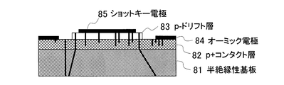
- FIG. 11 shows a conventional high-power diamond semiconductor element having a pseudo vertical structure.
- a p + contact layer 82 is grown on a semi-insulating diamond substrate 81, and a p ⁇ drift layer 83 is grown thereon to produce a laminated structure.
- an ohmic electrode 84 is provided on the p + contact layer 82 and a Schottky electrode 85 is provided on the p ⁇ drift layer 83 to produce an element.
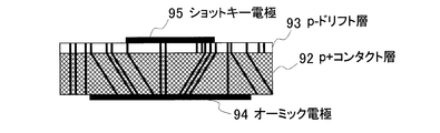
- FIG. 12 shows a conventional high-power diamond semiconductor device having a vertical structure using an HPHT / p + laminated substrate in which a p + layer is homoepitaxially grown on a high temperature / high pressure single crystal diamond.
- a p + contact layer 92 is used as the p + layer of the HPHT / p + laminated substrate, and a p ⁇ drift layer 93 is formed on the substrate to produce a laminated structure.
- the ohmic electrode 94 is formed on the surface of the p + contact layer 92 where the p ⁇ drift layer 93 is not formed, and the Schottky electrode 95 is formed on the p ⁇ drift layer 93.
- an element was manufactured.
- the present inventors have conducted research and development on a high-quality diamond laminated structure and manufacturing method by CVD (see Patent Documents 3 to 5).
- the inventors of the present invention performed ion implantation on the diamond substrate to form a layer having a modified crystal structure in the vicinity of the surface, and then performed diamond crystal growth on the substrate by a vapor phase synthesis method, and then the grown crystal layer
- a method for obtaining a self-supporting diamond CVD growth layer by separating the substrate and the substrate by electrochemical etching has been researched and developed (see Patent Documents 6, 7, and 8).
- Such a method for separating the crystal layer and the substrate is generally referred to as a smart cut method or a lift-off method.
- a structure in which a drift layer and a contact layer are stacked as an operating semiconductor layer is an essential structure.
- the contact layer is doped with a very high concentration of impurities in order to reduce parasitic resistance. For this reason, the contact layer has a problem in that the crystal quality is poor due to lattice distortion and dislocation.
- the drift layer it is necessary to extend the depletion layer when a reverse bias is applied and to maintain the voltage with a low leakage current even in a high electric field, so it is necessary to suppress the incorporation of defects in the element. Therefore, in order to perform a large current and high withstand voltage operation, the drift layer is required to have high crystallinity with low defect density and low distortion.
- a p + contact layer is grown on a semi-insulating diamond substrate with a thickness of 1 to 50 ⁇ m, and a p ⁇ drift layer is grown thereon with 1 to 20 ⁇ m ( (See FIG. 11).
- the drift layer is laminated on the contact layer by the CVD epitaxial growth method.
- FIG. 11 shows how defects (black thick lines) in the semi-insulating substrate 81 are taken over by the p + contact layer 82 and defects in the p + contact layer 82 are taken over by the p ⁇ drift layer 83.
- FIG. 12 shows how defects (black thick lines) in the p + contact layer 92 are taken over by the p ⁇ drift layer 93. For this reason, it is necessary to reduce the defect density in the drift layer. For this purpose, it is necessary to reduce the defect density of the p + contact layer, but it is difficult to reduce the defect density.
- the defect density in the drift layer is required to be 10 3 / cm 2 or less for a 1A class element and 10 2 / cm 2 or less for a 10 A class element.
- the drift layer is grown on the contact layer with many defects by high quality CVD.
- the dislocation there is a problem that it is difficult to take over the dislocation.
- FIG. 13 shows the relationship between the critical thickness of the p + contact layer and the boron concentration. Lines A and B indicate lines calculated using different models. As shown in FIG.
- the present invention is intended to solve these problems, and an object thereof is to provide a diamond electronic device having a drift layer with a reduced defect density. It is another object of the present invention to provide a method for manufacturing a diamond electronic device having a drift layer with reduced defect density.
- the present invention it is possible to form a high-quality drift layer by CVD epitaxial growth on ultra-high-quality single crystal diamond, and then grow a contact layer by high-concentration doping. As a result, a diamond electronic device with a reduced defect density of the drift layer was realized.
- the single crystal diamond substrate on which the drift layer is epitaxially grown is separated from the element portion by the smart cut method, thereby realizing a laminated structure.
- the present invention has the following features.
- a diamond electronic device has a laminated structure in which a structure holding material comprising semi-insulating single crystal diamond, a drift layer made of a diamond semiconductor, and a contact layer made of a diamond semiconductor are laminated in this order. And in addition, a cathode electrode is provided in the drift layer and an anode electrode is provided in the contact layer of the opening provided in the structure holding material.
- the drift layer is a p - diamond layer having a boron concentration of 10 15 / cm 3 or more and 10 17 / cm 3 or less, and the contact layer has a boron concentration of 10 19 / cm 3 or more. It is a p + diamond layer of 10 22 / cm 3 or less.
- a cathode electrode can be provided in an exposed portion where the drift layer is exposed.
- the cathode electrode may be formed of a laminated structure of an ohmic metal and an n + diamond layer
- the drift layer may be a p ⁇ diamond layer
- the contact layer may be a p + diamond layer.
- the drift layer has a thickness of 1 ⁇ m to 50 ⁇ m and the contact layer has a thickness of 1 ⁇ m to 100 ⁇ m.
- the semi-insulating single crystal diamond preferably has a dislocation density of 0 piece / cm 3 or more and 10 3 piece / cm 3 or less, and irregularities on the front and back surfaces are preferably Ra ⁇ 1 nm.
- the laminated structure preferably has a radius of curvature of 5 m or more and 500 m or less.
- the semi-insulating single crystal diamond is a nitrogen-containing single crystal diamond.
- the drift layer is formed by CVD synthesis on the semi-insulating single crystal diamond.
- the diamond electronic element of the first invention is a Schottky diode, a pn junction diode, or a pin junction diode.
- a drift layer made of a diamond semiconductor is formed on one surface of a semi-insulating single crystal diamond substrate, and the diamond semiconductor is made on the drift layer.
- Forming a contact layer; and forming an opening on the other surface of the semi-insulating single crystal diamond substrate by etching, and using the semi-insulating single crystal diamond substrate as a structure holding material, a part of the drift layer is formed A step of forming an exposed exposed portion; and a step of providing a cathode electrode on the exposed portion and an anode electrode on the contact layer.
- a method for manufacturing a diamond electronic device comprising: forming a drift layer made of a diamond semiconductor by providing an n + diamond layer on one surface of a semi-insulating single crystal diamond substrate; Forming a contact layer made of a diamond semiconductor on the surface, and forming an opening on the other surface of the semi-insulating single crystal diamond substrate by etching, and using the semi-insulating single crystal diamond substrate as a structure holding material; + A step of forming an exposed portion where a part of the diamond layer is exposed; and a step of forming an ohmic metal in the exposed portion to form a cathode electrode and providing an anode electrode in the contact layer.
- a diamond electronic device is a diamond electronic device comprising a drift layer made of a diamond semiconductor, a structure holding material having a semi-insulating diamond layer, and a contact layer made of a diamond semiconductor,
- the structure holding material has an opening and is laminated on one surface of the drift layer, and the contact layer is laminated directly on the drift layer in the opening.
- the electrode is characterized in that an anode electrode is provided on the contact layer in the opening and a cathode electrode is provided on the other surface of the drift layer.
- the contact layer and the anode electrode may be disposed only in the opening, or may be laminated on a structure holding material other than the opening.
- the drift layer is a p ⁇ diamond layer and the contact layer is a p + diamond layer.
- the drift layer is a p - diamond layer having a boron concentration of 10 15 / cm 3 or more and 10 17 / cm 3 or less, and the contact layer has a boron concentration of 10 19 / cm 3 or more and 10 22 / cm 3. It is below, and it is preferable that it is a p + diamond layer.
- the electronic element of the second invention of the present invention preferably has a curvature radius of 5 m or more and 500 m or less.
- the cathode electrode is formed of a laminated structure of an ohmic metal and an n + diamond layer, the drift layer is a p ⁇ diamond layer, and the contact layer is a p + diamond layer. Is preferred.
- the drift layer has a thickness of 1 ⁇ m to 50 ⁇ m and the contact layer has a thickness of 1 ⁇ m to 100 ⁇ m.
- the semi-insulating diamond layer of the second invention of the present invention is preferably nitrogen-containing homoepitaxial single crystal diamond or nitrogen-containing polycrystalline diamond.
- the diamond electronic device of the second invention of the present invention is, for example, a Schottky diode, a pin junction diode, or a pn junction diode.
- a method for manufacturing a diamond electronic device comprising: forming a drift layer on a substrate surface after forming a defect layer on one substrate surface of a single crystal diamond substrate; Forming a structure holding material having an opening by selectively growing the semi-insulating diamond layer on the layer; separating the single crystal diamond substrate and the drift layer by the defect layer; and Etching the layer to separate the drift layer, exposing the drift layer, and forming the contact layer on the drift layer in the opening.
- the method for manufacturing a diamond electronic device of the second invention includes a step of providing a cathode electrode in the drift layer and providing an anode electrode in the contact layer of the opening.
- the single crystal diamond substrate preferably has a dislocation density of 10 3 pieces / cm 2 or less, and irregularities on the front surface and the back surface satisfy Ra ⁇ 1 nm.
- the drift layer is preferably formed on the single crystal diamond substrate by CVD synthesis.
- Defects in the diamond epitaxial film are caused by inheritance from the base substrate and generation by lattice strain relaxation during the epitaxial process.
- the defect density of the drift layer is increased by using a substrate or contact layer having a high-density defect as a base. Even when a single crystal substrate with low defects was used as the substrate, the defect density of the drift layer was high due to defects generated by lattice relaxation in the contact layer.
- high-quality semi-insulating single crystal diamond is used as a structure holding material, and a drift layer made of a diamond semiconductor and a contact layer made of a diamond semiconductor are laminated on the structure holding material in this order by epitaxial growth.
- a drift layer in which defects inherited from the base substrate and defects generated in the film are reduced can be realized. That is, directly in the high-quality semi-insulating single-crystal diamond substrate p - drift layer is epitaxially grown, to grow then p + contact layer, p - / p + have a stacked structure p - defect density of the drift layer Can be greatly reduced. According to the laminated structure of the first aspect of the present invention, a high voltage operation with a high-quality drift layer can be realized at the same time with an element capable of high current operation with low parasitic resistance.
- the laminated structure of the second invention of the present invention makes it possible to grow and form a drift layer made of a diamond semiconductor directly on a single crystal diamond substrate to be removed in the manufacturing process. Can be formed.
- a defect layer is introduced by ion implantation. However, dislocation does not occur even when the defect layer is introduced, and the p ⁇ drift layer maintains a low defect.
- a semi-insulating diamond is used as the structure holding material, a diamond semiconductor contact layer can be formed.
- the structure holding material having an opening is selectively grown on the drift layer using a lithography technique, the curvature of the wafer due to the lamination of different impurity concentration layers can be reduced.
- a thin p ⁇ drift layer / p + contact layer stacked structure can be sufficiently maintained without damaging the diamond substrate.
- the p ⁇ drift layer is directly epitaxially grown on the high quality semi-insulating single crystal diamond substrate which is later removed by the smart cut method, and then the p + contact layer is grown. since it was possible that, p - / p + have a stacked structure p - the defect density of the drift layer can be reduced significantly.
- a high voltage operation by a high-quality drift layer can be realized simultaneously with an element capable of high current operation with low parasitic resistance.
- the figure which shows the laminated structure of the diamond electronic element of 1st invention The figure explaining the laminated structure and defect of the diamond electronic element of Example 1.
- Characteristics of the diamond electronic device having the high-quality p ⁇ drift layer of Example 1 The figure which shows the laminated structure of the diamond electronic element of Example 1
- the figure which shows the laminated structure of the diamond electronic element of Example 3 The figure which shows the manufacturing method of the diamond electronic element of Example 3.
- FIG. 1 shows a typical example of the laminated structure of the diamond electronic element of the first invention.
- the substrate 1 having an opening for electrode arrangement is used as a structure holding material.
- a diamond electronic device according to a first aspect of the present invention has a structure in which a structure holding material made of a substrate 1, a drift layer (p ⁇ layer 2), and a contact layer (p + layer 3) are sequentially stacked.
- An electrode Schottky electrode 5
- An electrode is provided in contact with the exposed drift layer (p ⁇ layer 2) in the opening provided on the surface of the holding material where the drift layer and the contact layer are not formed.
- An electrode (ohmic electrode 4) is provided on (p + layer 3).
- a high-quality single crystal diamond substrate having a controlled low off-angle and off-direction and having a low surface defect density is used as the substrate used as the structure holding material.
- the substrate off-angle control is preferably such that the ⁇ 001> vector has an off-angle of 1 ° or more with respect to the surface normal vector in the ⁇ 110> ⁇ 5 ° direction (see Patent Document 2).
- a substrate whose both surfaces are polished with high precision and whose surface and back surface have an unevenness of Ra ⁇ 1 nm is used. This is to reduce the defects in the diamond layer formed by CVD synthesis on it and suppress the generation of etch pits during etching.
- Ra represents arithmetic average roughness and is defined by JIS B0601: '01 standard.
- a p ⁇ drift layer is epitaxially grown by CVD on a substrate used as a structure holding material.
- the p ⁇ drift layer is 1 ⁇ m or more and 50 ⁇ m or less.
- the boron concentration in the film is preferably 10 15 / cm 3 or more and 10 17 / cm 3 or less.
- a p + contact layer is epitaxially grown on the epitaxially grown p ⁇ drift layer by a CVD method to produce a stacked structure.
- p + In forming the contact layer, suppressing the crystal defects formed by distortion of the substrate, and in order to lower resistance, p + contact layer with a thickness of 100 ⁇ m or more 1 ⁇ m 5 ⁇ 10 19 / cm 3 or more 10 22 A boron concentration of / cm 3 or less is preferable.
- the curvature radius of the wafer is preferably 5 m or more and 500 m or less.
- the opening of the structure holding material is formed by forming an etching mask pattern on the high-quality single crystal diamond substrate surface side using lithography and performing etching.
- Etching mask SiO 2, Al, Al 2 O 3, etc. Mo are preferable.
- etching is performed using O 2 gas to which a small amount of CF 4 , CHF 3 , SF 6 or the like is added. Is preferred.
- Ar and Xe as etching gases. Etching is performed until the p ⁇ drift layer is exposed.
- annealing and a hot mixed acid cleaning treatment are performed to remove a defective layer by etching. Further, an ohmic electrode is formed on the p + contact layer, and a Schottky electrode is formed on the p ⁇ drift layer to form an element. An n-type layer is formed on the Schottky edge to form an electric field relaxation structure.
- the drift layer is epitaxially grown on the high-quality substrate and then the contact layer is grown, the defect density of the drift layer can be greatly reduced.
- a p ⁇ drift layer and a p + contact layer with few defects can be epitaxially grown sequentially on a high-quality substrate, and the thickness of the contact layer is less than the film thickness limit where dislocation occurs. Can be thinned.
- Embodiment 2 of the present invention will be described below.
- FIG. 7 shows the basic structure of the laminated structure of the diamond electronic element of the second invention.
- a semi-insulating diamond layer having an opening for electrode arrangement is used as a structure holding material (also called a structure holding layer).
- a diamond electronic device includes a drift layer (p ⁇ layer (also referred to as a p ⁇ drift layer) 62) made of a diamond semiconductor, a structure holding layer 61 having a semi-insulating diamond layer, a contact layer made of a diamond semiconductor ( It has a stacked structure in which p + layers (also referred to as p + contact layers) 63) are stacked in this order.
- the structure retaining layer 61 has an opening, and the drift layer (p ⁇ layer 62) and the contact layer (p + layer 63) are directly stacked in the opening.
- the electrodes are arranged so that a cathode electrode (Schottky electrode) is provided on the drift layer (p ⁇ layer 62) and an anode electrode (ohmic electrode) is provided on the contact layer (p + layer 63) in the opening. .
- a layer (defect layer) having a modified crystal structure is formed in the vicinity of the surface by ion implantation on a high-quality single crystal diamond (001) substrate having low surface defects and controlled in off angle and off direction. After that, crystal growth is performed on the substrate by a vapor phase synthesis method, and then the grown crystal layer and the substrate are separated.
- a method for forming a defect layer by ion implantation and a method for separating the crystal layer and the substrate known methods such as the methods disclosed in Patent Documents 6 and 7 can be used.
- ions used for ion implantation hydrogen, carbon, or the like can be used.
- the substrate has an off angle of 2 ° in the ⁇ 110> direction in order to perform flat epitaxial growth, but the variation is within ⁇ 5 ° in the ⁇ 110> direction, and the ⁇ 001> vector becomes the normal vector of the surface. In contrast, those having an off angle of 1 ° or more are preferable.
- Ra represents arithmetic average roughness and is defined by JIS B0601: '01 standard.
- a p ⁇ diamond layer (drift layer) is epitaxially grown on the substrate by CVD.
- the p ⁇ drift layer is 1 ⁇ m or more and 50 ⁇ m or less.
- the boron concentration in the film is preferably 10 15 / cm 3 or more and 10 17 / cm 3 or less.
- the curvature radius of the wafer is preferably 5 m or more and 500 m or less.
- the CVD method is performed using microwave plasma, using a gas of any one of H 2 , CO 2 , and CH 4 and, in some cases, a mixed gas of trimethyl boron (TMB).
- the second invention is characterized by a laminated structure including a structure holding material and a manufacturing method.
- a mask is formed on the p ⁇ drift layer formed on the substrate using a lithography technique, and a diamond film as a structure holding material is selectively formed by a CVD method.
- the material used for the mask is preferably SiO 2 or Ti / Au.
- the diamond film serving as the structure holding material is preferably semi-insulating and is a nitrogen-containing homoepitaxial single crystal film or a nitrogen-containing polycrystalline film.
- the crystal layer and the substrate were separated using the method described in Patent Document 8.
- the above-mentioned laminated diamond was put in ultrapure water, a voltage of 5.6 kV was applied between platinum electrodes that were also put in ultrapure water, and left for 15 hours, whereby the defect layer was separated by electric field etching.
- the mask is removed by acid cleaning, and a p + contact layer is epitaxially grown on the peeling surface side (side from which the mask of the structure holding layer is peeled) by the CVD method.
- p + In forming the contact layer, suppressing the crystal defects formed by distortion of the substrate, and in order to lower resistance, p + contact layer with a thickness of 100 ⁇ m or more 1 ⁇ m 5 ⁇ 10 19 / cm 3 or more 10 22 A boron concentration of / cm 3 or less is preferable.
- the curvature radius of the wafer is preferably 5 m or more and 500 m or less.
- the drift layer is epitaxially grown on the high-quality substrate, and then the contact layer is grown via the structure holding layer, so that the defect density of the drift layer can be greatly reduced.
- a p ⁇ drift layer and a p + contact layer with few defects can be epitaxially grown on a high-quality substrate, and the thickness of the contact layer is reduced below the film thickness limit where dislocation occurs. be able to.
- Example 1 A diamond electronic device of Example 1 relating to the first invention of the present invention will be described below with reference to FIGS.
- FIG. 2 is a view showing a laminated structure and defects of the diamond electronic device of this example
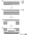
- FIG. 3 is a view showing a manufacturing process. With reference to FIG. 3, the manufacturing process of the diamond electronic element of a present Example is demonstrated.
- a 3 ⁇ 3 mm high quality semi-insulating single crystal diamond (001) Ib substrate with controlled low off-angle and off-direction and low surface defect density was adjusted to a thickness of 100 ⁇ m.
- the ⁇ 001> vector has an off-angle of 2.5 ° with respect to the surface normal vector in the ⁇ 110> direction.
- the dislocation density is about 10 4 / cm 2 and the half width of the XRD (004) rocking curve is 7 arcsec or less.
- a p ⁇ drift layer 2 is epitaxially grown on the substrate by CVD (see FIG. 3A).
- the drift layer was epitaxially grown by CVD using a 2.45 GHz microwave in an environment of 120 Torr and 3900 W.
- the CH 4 flow rate was 16 sccm with respect to the H 2 flow rate 384 sccm, and the total flow rate was 400 sccm.
- the synthesis time is 10 hours and the film thickness is 25 ⁇ m.
- the boron concentration in the film was about 10 16 / cm 3 due to boron incorporation from the chamber environment.
- the p + contact layer 3 is epitaxially grown by microwave plasma CVD (see FIG. 3B).
- the H 2 flow rate was 390 sccm
- the CH 4 flow rate was 4 sccm
- trimethylboron (TMB) hydrogen 1% dilution
- the plasma output was 1500 W.
- the p + contact layer is 30 ⁇ m thick and has a boron concentration of 2 ⁇ 10 20 / cm 3 .
- a mask was formed on the back side of the substrate using a photolithography technique, and the p ⁇ drift layer was selectively exposed by an etching method (see FIG. 3C).
- SiO 2 is formed to a thickness of 0.8 ⁇ m on the entire surface of the substrate by tetraethoxysilane (TEOS) / CVD.
- TEOS tetraethoxysilane
- a resist is opened by photolithography.
- the openings have a rounded structure of 500 ⁇ m and are arranged in a lattice pattern at a pitch of 750 ⁇ m, but this region finally becomes a Schottky electrode region and is designed according to the required device current.
- As the resist AZ5214E made by Clariant Co.
- a high-quality semi-insulating single crystal diamond (001) Ib substrate is formed by selectively etching SiO 2 in the resist opening using CF 4 gas by ICP (reactive ion etching using capacitively coupled plasma). Expose the surface.
- the plasma conditions were as follows: a bias of 20 W was applied at a plasma output of 200 W, and CF 4 gas was 20 sccm and a pressure of 2 Pa.
- the resist used for the mask is removed by acetone treatment and O 2 plasma ashing.
- the diamond in the opening was etched using the selectively formed SiO 2 as a mask. Etching was also performed using the ICP method and O 2 gas plasma.
- the plasma conditions were 700 W plasma output, 250 W bias applied, and O 2 gas 100 sccm at 2 Pa pressure.
- the etching process was performed until the drift layer was exposed, and the current characteristics were evaluated on the front and back of each etching to confirm the exposure of the drift layer.
- the element diamond substrate is subjected to mixed acid cleaning to perform oxygen termination and remove non-diamond components.
- a Ti / Pt / Au ohmic electrode 4 is formed on the p + contact layer, and annealing treatment is performed at 420 ° C. for 1 hour in an Ar atmosphere to reduce the contact resistance (see FIG. 3D).
- FIG. 4 shows the withstand voltage characteristics of the manufactured Schottky barrier diode element.
- the horizontal axis in FIG. 4 represents the withstand voltage (V), and the vertical axis represents the leakage current (A).
- the leakage current is a current at the time of withstand voltage measurement, and is a leakage current of the entire element.
- FIG. 4 shows the leakage current characteristics with respect to the reverse voltage of the element of this example.
- the leakage current of the device of this example is less than the measurement limit value (10 ⁇ 13 A) in the region up to 2200 V, which is the measurement range, and is excellent in the withstand voltage characteristics.
- the drift layer is epitaxially grown, growing then p + contact layer, p - - in the structure of the first aspect of the invention, directly to the high-quality substrate p / p + be a laminate structure, p - defect of the drift layer
- the density can be greatly reduced. It was an element capable of high current operation with a low parasitic resistance due to the laminated structure, and was able to simultaneously realize high voltage operation with a high-quality drift layer.
- FIG. 5 shows and describes the laminated structure of the diamond electronic device of this example.
- the diamond electronic device of this example has a structure in which a structure holding layer 11, a p ⁇ diamond layer 12, and a p + diamond layer 13 are sequentially laminated.
- a cathode (Schottky electrode) 15 is provided, and an anode (ohmic electrode) 14 is provided on the p + diamond layer 13.
- the p ⁇ diamond layer 12 needs to control the doping concentration and film thickness of the drift layer in order to operate the diode at a high voltage and low leakage, and to operate at a low on-resistance, and the boron concentration is 10 15 / It is preferable that it is cm 3 or more and 10 17 / cm 3 or less.
- the thickness of the p ⁇ drift layer is preferably 1 ⁇ m or more and 50 ⁇ m or less.
- the p + diamond layer 13 has a boron concentration of 10 19 / cm 3 or more and 10 22 / cm 3 in order to suppress the formation of crystal defects due to the distortion of the substrate and reduce the resistance when forming the p + contact layer.
- the film thickness is 1 ⁇ m or more and 100 ⁇ m or less, and the curvature radius of the wafer is preferably 5 m or more and 500 m or less in order to prevent a significant increase in cracks and defects of the wafer.
- a self-standing single crystal diamond substrate synthesized by CVD can be used as the structure holding material.
- the semi-insulating single crystal diamond is, for example, nitrogen-containing single crystal diamond.
- the semi-insulating single crystal diamond substrate suitable for the structure holding material preferably has a dislocation density of 0 / cm 3 or more and 10 3 / cm 3 or less.
- Example 2 The laminated structure of the diamond electronic element of Example 2 relating to the first invention of the present invention will be described in detail below with reference to FIG.
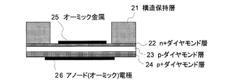
- the diamond electronic device of Example 2 has a structure in which a structure holding layer 21, an n + diamond layer (also referred to as an n + layer) 22, a p ⁇ diamond layer 23, and a p + diamond layer 24 are sequentially stacked.
- An ohmic metal 25 is provided in the opening of the structure holding layer, and an n + diamond layer and an ohmic metal layer have a cathode electrode function.
- the p + diamond layer 24 is provided with an anode (ohmic electrode) 26.
- the structure holding layer 21 uses the same substrate as in the first embodiment.
- the n + diamond layer 22 preferably has a doping impurity concentration of 10 15 / cm 3 or more and 10 17 / cm 3 or less in order to reduce on-resistance and ohmic resistance.
- the doping impurity used for the n + diamond layer 22 is phosphorus, but may be sulfur or lithium.
- the p ⁇ diamond layer 23 preferably has a boron concentration of 10 15 / cm 3 or more and 10 17 / cm 3 or less in order to operate the diode with a high voltage and low leakage and further to operate with a low on-resistance.
- the p + diamond layer 24 preferably has a boron concentration of 10 19 / cm 3 or more and 10 22 / cm 3 or less in order to achieve a low on-resistance. Further, in order to prevent the wafer from cracking and a significant increase in defects, the wafer having the above laminated structure preferably has a curvature radius of 5 m or more and 500 m or less.
- the ohmic metal 25 of the cathode electrode is formed of Au (100 nm) / Pt (30 nm) / Ti (30 nm), and the anode (ohmic electrode) 26 is formed of Au (100 nm) / Pt (30 nm) / Ti (30 nm). In the diamond electronic device shown in FIG.
- Example 6 after forming the layers in the order of structure-retaining layer (substrate) / n + diamond layer / p ⁇ diamond layer / p + diamond layer, the processing steps and exposure are the same as in Example 1. A part forming step and an oxygen termination treatment step were performed, and then an electrode was formed. In the electrode forming step, a Ti / Pt / Au ohmic electrode was formed on the p + contact layer in the same manner as in Example 1 to reduce the contact resistance. The ohmic metal was formed on the n + diamond layer exposed at the opening to form a cathode electrode. In addition to the structure shown in FIG.
- the cathode electrode layered structure is formed on the drift layer exposed to the opening by forming a layered structure similar to that in Example 1 and then forming an opening in the structure holding material.
- an n + diamond layer and an ohmic metal may be formed.
- an n + diamond layer and an ohmic metal may be provided not only on the opening but also on the structure holding material.
- the element of Example 2 can be used as a power device for a rectifying diode semiconductor element.
- Example 3 A diamond electronic device of Example 3 relating to the second invention of the present invention will be described below with reference to FIGS.
- FIG. 7 is a diagram showing a laminated structure of diamond electronic elements of this example
- FIG. 8 is a diagram showing a manufacturing process. With reference to FIG. 8, the manufacturing process of the diamond electronic element of a present Example is demonstrated.
- the single crystal diamond substrate is a chemical vapor deposition (CVD) diamond by microwave of 12 mm size formed by a smart cut method, and has a dislocation density of about 5 ⁇ 10 2 / cm 2 and an XRD (004) rocking curve.
- the half width is 10 arcsec or less.
- ap ⁇ drift layer 62 was epitaxially grown on the substrate 66 by the CVD method.
- the drift layer was epitaxially grown in an environment of 120 Torr and 3900 W by CVD using 2.45 GHz microwave.
- the CH 4 flow rate was 16 sccm with respect to the H 2 flow rate of 384 sccm, and the total flow rate was 400 sccm.
- the synthesis time was 18 hours and the film thickness was 45 ⁇ m.
- the boron concentration in the film was about 1 ⁇ 10 16 / cm 3 due to boron incorporation from the chamber environment.
- the light emission region is about 7 ⁇ 10 2 / cm 2 , and hardly increases. From this, it can be seen that there is no dislocation or defect in the second invention.
- SiO 2 having a thickness of 0.8 ⁇ m was formed on the entire surface of the substrate by tetraethoxysilane (TEOS) / CVD. Further, the resist in the selective growth portion was opened by photolithography. As the resist, AZ5214E made by Clariant Co. having a thickness of 3 ⁇ m was used. The SiO 2 in the opening portion of the resist was selectively etched using CF 4 gas by ICP method (reactive ion etching using capacitively coupled plasma) to expose the diamond surface. As for the plasma conditions, a bias of 20 W is applied at a plasma output of 200 W, and a pressure of 2 Pa is obtained with 20 sccm of CF 4 gas.
- ICP method reactive ion etching using capacitively coupled plasma
- the resist was removed by acetone treatment and O 2 plasma ashing.
- the resist portion has a rounded structure of 250 ⁇ m and is arranged in a lattice pattern at a pitch of 750 ⁇ m. This region is a portion that finally becomes an opening of the structure holding material, and a portion that becomes an ohmic electrode region. Design according to the required device current.
- diamond was selectively grown using SiO 2 selectively formed by etching as a mask.
- the selective growth of diamond was performed using a microwave CVD method with a CH 4 flow rate of 16 sccm with respect to an H 2 flow rate of 384 sccm.
- hydrogen to which N 2 gas was added was used, and the added nitrogen was 100 ppm in N / C.
- the film thickness of the structure holding material was 30 ⁇ m, and the nitrogen concentration in the film was 2 ⁇ 10 17 / cm 3 .
- the selective growth mask and dust are removed by washing with HF and sulfuric acid / hydrogen peroxide, and the seed substrate 66 and element diamond (p - drift layer 62 and structure retaining layer) are separated by defect layers by the smart cut method (FIG. 8).
- C Separation was performed in pure water, and a voltage of 5.6 kV was applied to the opposed platinum electrodes and left for 15 hours to separate the electrodes.
- the defect layer 67 was removed by performing an ICP etching process using Ar gas on the entire surface of the element diamond separation surface at a depth of 2 ⁇ m.
- a p + contact layer is epitaxially grown on the structure holding layer of the device diamond by the microwave plasma CVD method (FIG. 8D).
- the H 2 flow rate was 390 sccm
- the CH 4 flow rate was 4 sccm
- TMB 1% hydrogen dilution
- the plasma output was 1500 W.
- the p + contact layer had a thickness of 10 ⁇ m and a boron concentration of 2 ⁇ 10 20 / cm 3 .
- the element diamond substrate is subjected to mixed acid cleaning and oxygen termination, and non-diamond components adhering to the diamond surface during synthesis are removed.
- FIG. 8E shows an electrode forming process.
- FIG. 8E is a diagram in which the top and bottom of FIG. 8D are displayed upside down.
- An ohmic electrode 64 of Ti / Pt / Au is formed on the p + contact layer 63 and annealed at 420 ° C. for 1 hour in an Ar atmosphere to reduce the contact resistance (see FIG. 8E).
- a Ru Schottky electrode 65 having a round shape of 300 ⁇ m and a thickness of 100 nm was formed on the p ⁇ drift layer 62 side to form a Schottky barrier diode element (see FIG. 8E).
- FIG. 7 shows a modification of the diamond electronic element of Example 3 below with reference to FIG. 7 in the structure holding layer 61 excluding the opening.
- a drift layer p ⁇ drift layer 62
- a structure holding layer 61 having a semi-insulating diamond layer a contact layer (p + contact made of a diamond semiconductor).
- a contact layer and the anode electrode positioned other than the opening are not essential and can be appropriately arranged according to the electrode structure and the like.
- FIG. 9 shows a modification in which a contact layer (p + contact layer 63) and an anode electrode (ohmic electrode) 64 are provided only in the opening.
- the diamond electronic device of Example 4 includes an n + layer (also referred to as an n + diamond layer) 71 made of a diamond semiconductor, and a p ⁇ layer (also called a p ⁇ drift layer or a p ⁇ diamond layer) 72 made of a diamond semiconductor.
- the structure holding layer 61 and a p + layer (also referred to as a p + contact layer, also referred to as p + diamond layer) 73 made of a diamond semiconductor are sequentially stacked.
- n + layer 71 On the p + layer 73 at the opening of the structure holding layer, An anode (ohmic electrode) 74 is provided, and an ohmic metal 75 is provided on the n + layer 71 to form a cathode.
- a film similar to that in Example 3 is used.
- the n + layer 71 preferably has a doping impurity concentration of 10 17 / cm 3 or more from the viewpoint of reducing on-resistance and ohmic resistance. Further, in order to reduce the introduction of defects into the crystal due to strain, it is preferably 10 22 / cm 3 or less.
- the curvature radius of the wafer is preferably 5 m or more and 500 m or less.
- the p ⁇ drift layer 72 preferably has a boron concentration of 10 15 / cm 3 or more and 10 17 / cm 3 or less in order to maintain a high reverse withstand voltage and to reduce the on-resistance as much as possible.
- the p + contact layer 73 preferably has a doping impurity concentration of 10 17 / cm 3 or more in order to reduce on-resistance and ohmic resistance.
- the anode (ohmic electrode) 74 is formed of Au (100 nm) / Pt (30 nm) / Ti (30 nm), and the cathode ohmic metal 75 is formed of Au (100 nm) / Pt (30 nm) / Ti (30 nm).
- Example 4 The laminated structure of Example 4 is manufactured by the same process as that shown in Example 3. However, in addition to the step of forming the p + contact layer (p + contact layer 63) of Example 3, the n + diamond layer 71 is formed on the opposite side of the p + contact layer from the substrate.
- the element of Example 4 can be used as a power device for a rectifying diode semiconductor element.
- the drift layer is a p ⁇ diamond layer
- the contact layer is a p + diamond layer (Examples 1 and 3)
- the cathode electrode is formed of a laminated structure of an ohmic metal and an n + diamond layer.
- the drift layer is a p ⁇ diamond layer and the contact layer is a p + diamond layer.
- the interface between the p ⁇ drift layer and the n + diamond layer is shown.
- a pin structure in which an i layer having an impurity concentration of 10 12 / cm 3 or less is sandwiched can be formed.
- the drift layer refers to a layer in which a depletion layer expands when a reverse voltage is applied and maintains a withstand voltage
- the contact layer refers to a forward voltage that does not expand even when a reverse voltage is applied due to a high impurity concentration.
- the diamond electronic device of the present invention can be used as semiconductor devices such as various diodes such as Schottky diodes, pn junction diodes, and pin junction diodes, thyristors, and FETs.
Landscapes
- Electrodes Of Semiconductors (AREA)
Abstract
ドリフト層をダイヤモンド基板上に直接成膜することにより、欠陥密度が低減したドリフト層を有する高出力ダイヤモンド電子素子を提供する。半絶縁性単結晶ダイヤモンドを備える構造保持材、ダイヤモンド半導体からなるドリフト層、ダイヤモンド半導体からなるコンタクト層の順に積層された積層構造を有するダイヤモンド電子素子であり、構造保持材に設けた開口部においてドリフト層にカソード電極を設ける構造とする。又は、ダイヤモンド半導体からなるドリフト層と、半絶縁性ダイヤモンド層を有する構造保持材と、ダイヤモンド半導体からなるコンタクト層とを備えるダイヤモンド電子素子であり、構造保持材は、開口部を有し、ドリフト層の一方の面に積層されており、コンタクト層は、開口部内において、ドリフト層に直接積層されており、アノード電極は、開口部内のコンタクト層に設け、カソード電極はドリフト層の他方の面に設けた構造とする。
Description
本発明は、縦型構造のダイオード、トランジスタ、FET、サイリスタ等の高出力のダイヤモンド電子素子及びその製造方法に関する。
近年、ダイヤモンド電子素子は、大きなバンドギャップ、高いアバランシェ破壊電界、高い飽和キャリア移動度、高い熱伝導率、高温度や放射線曝露環境下で実用動作可能な素子として期待されている。これらの特徴を生かした半導体素子として、ダイヤモンドショットキーバリアダイオード、ダイヤモンド電界効果トランジスタ、ダイヤモンドpnダイオード、ダイヤモンドサイリスタ、ダイヤモンドトランジスタなどの高出力ダイヤモンド半導体素子の開発が進められている。
従来、高出力ダイヤモンド半導体素子の積層構造のうち擬似縦型構造(特許文献1、2、非特許文献1~3参照)や縦型構造(非特許文献4~7参照)について、本発明者等を含め研究開発がなされてきた。
従来の擬似縦型構造の高出力ダイヤモンド半導体素子を図11に示す。図11のように、半絶縁性ダイヤモンド基板81にp+コンタクト層82を成長させ、その上にp-ドリフト層83を成長させて積層構造を作製していた。該積層構造に、オーミック電極84をp+コンタクト層82上に設け、ショットキー電極85をp-ドリフト層83上に設けて素子を作製していた。
従来の、高温高圧単結晶ダイヤモンド上にp+層をホモエピタキシャル成長させたHPHT/p+積層基板を用いた縦型構造の高出力ダイヤモンド半導体素子を、図12に示す。図12のように、HPHT/p+積層基板のp+層をp+コンタクト層92とし、該基板の上にp-ドリフト層93を成膜して積層構造を作製していた。該積層構造において、p-ドリフト層93が成膜されていない方のp+コンタクト層92面に、オーミック電極94を形成し、一方、p-ドリフト層93の上に、ショットキー電極95を形成して、素子を作製していた。
また、本発明者等は、CVDによる高品質ダイヤモンド積層構造及び製法について研究開発を行ってきた(特許文献3~5参照)。また、本発明者等は、ダイヤモンド基板にイオン注入を行って表面近傍に結晶構造の変質した層を形成した後、気相合成法により基板上にダイヤモンド結晶成長を行い、次いで、成長した結晶層と基板とを電気化学的なエッチングにより分離させることにより、自立したダイヤモンドCVD成長層を得る方法を研究開発した(特許文献6、7、8参照)。このような結晶層と基板との分離方法は一般にスマートカット法もしくはリフトオフ法と称される。
H.Umezawa et al.IEEE Electron Device Lett.30(2009)960.
S.Shikata et al.Mater.Sci.Forum,615-617(2009)999.
K.Ikeda et al.Appl.Phys.Express,2(2009)011202.
A. Vescan et al. Diam. Relat. Mater. 7 (1998) 581.
W.Ebert et al.Diam.Relat.Mater.6(1997)329.
S.J.Rashid,Proc.ISPSD’08(2008)249.
M.Imura et al.Diam.Relat.Mater.17(2008)1916.
高出力半導体素子を作製するためには、動作半導体層としてドリフト層、コンタクト層を積層させる構造が必須の構造である。コンタクト層は寄生抵抗を減らすために、非常に高濃度の不純物ドーピングがなされる。そのため、コンタクト層には、格子ひずみや転位が発生し結晶品質が悪いという問題があった。一方、ドリフト層については、逆バイアス印加時に空乏層を伸張させて高電界でも低リーク電流で電圧維持する必要があるので、素子中の欠陥混入を抑える必要がある。そのため、大電流かつ高耐電圧動作を行うために、ドリフト層には、低欠陥密度で歪が少ない高い結晶性が求められる。
従来の擬似縦型構造を用いた場合では、半絶縁性ダイヤモンド基板上にp+コンタクト層を1~50μmの厚さで成長させ、その上にp-ドリフト層を1~20μm成長させている(図11参照)。ここで、ドリフト層をコンタクト層上へCVDエピタキシャル成長法によって積層させているが、高品質が求められるドリフト層を、欠陥が多く品質が悪いコンタクト層上へ成長させた場合には、コンタクト層内に存在する欠陥がドリフト層中にも引き継がれるために、ドリフト層の品質が悪くなる。図11に、半絶縁性基板81の欠陥(黒太線)がp+コンタクト層82に引き継がれ、p+コンタクト層82の欠陥がp-ドリフト層83に引き継がれる様子を示した。
また、従来のHPHT/p+基板を用いた場合では、IIb型HPHTダイヤモンドなどの低抵抗単結晶基板も存在するが、基板自体の転位も多く基板サイズも小さいため、素子の大型化は不可能である。基板の転位はデバイス特性に影響を与えると考えられ、実際に素子サイズを大きくすると、素子特性が劣化する現象が見られる。図12に、p+コンタクト層92の欠陥(黒太線)がp-ドリフト層93に引き継がれる様子を示した。このことから、ドリフト層中の欠陥密度の低減が必要である。そのためにはp+コンタクト層の欠陥密度低減が必要であるが、欠陥密度低減は困難であった。なお、ダイヤモンドでは1A級の素子にはドリフト層中の欠陥密度を103個/cm2以下、10A級の素子には102個/cm2以下とする必要がある。
このように、素子特性の改善や高出力化にはドリフト層中に存在する転位などの欠陥密度を下げる必要があるのに、欠陥の多いコンタクト層上にドリフト層を高品質でCVD成長させるのは、転位の引継ぎのため難しいという問題がある。
また、オン抵抗を低く保つためには、p+コンタクト層のドーピング濃度を高くし、p+コンタクト層の寄生抵抗成分を低くすることが必要であるが、ドーピング濃度を高くすることによって、p+コンタクト層とp-ドリフト層の格子定数に差が発生し、これにより基板に反りが生じる。反りが発生している状態でp-ドリフト層を積層させると欠陥が発生する。コンタクト層濃度に対して、欠陥のひとつである転位が導入される膜厚限界が存在する。図13に、p+コンタクト層の臨界厚さとホウ素濃度との関係を示す。線AとBは異なるモデルで計算した線を示す。図13に示すとおり、金属的伝導が得られる高濃度ドーピング(>1020/cm3)レベルで10μm以下にする必要がある。しかし、この厚さのコンタクト層を擬似縦型構造に用いた場合には横方向に電流を流すために寄生抵抗が高くなり、一方、縦型構造に用いた場合では薄すぎて構造維持ができない。また、ウェハや素子の品質は、歪みを指標にすることが可能であり、その反りは曲率半径で示され、曲率半径の大きいものほど反りが小さく品質が良い。
本発明は、これらの問題を解決しようとするものであり、欠陥密度が低減したドリフト層を有するダイヤモンド電子素子を提供することを目的とする。また、欠陥密度が低減したドリフト層を有するダイヤモンド電子素子を製造するための方法を提供することを目的とする。
本発明の第1及び第2の発明では、高品質のドリフト層を超高品質単結晶ダイヤモンド上にCVDエピタキシャル成長させ、その後に高濃度ドーピングによりコンタクト層を成長させて形成することを可能とした構造により、ドリフト層の欠陥密度が低減したダイヤモンド電子素子を実現した。また、第2の発明では、ドリフト層をエピタキシャル成長させた単結晶ダイヤモンド基板を、スマートカット法により素子部より分離することにより、積層構造を実現した。本発明は、前記目的を達成するために、以下の特徴を有する。
本発明の第1の発明のダイヤモンド電子素子は、半絶縁性単結晶ダイヤモンドを備える構造保持材、ダイヤモンド半導体からなるドリフト層、ダイヤモンド半導体からなるコンタクト層の順に積層された積層構造を有することを特徴とする。また、前記構造保持材に設けた開口部の、前記ドリフト層にカソード電極を設け、前記コンタクト層にアノード電極を設けたことを特徴とする。具体的な構造の例として、前記ドリフト層は、ホウ素濃度が1015/cm3以上1017/cm3以下のp-ダイヤモンド層であり、前記コンタクト層は、ホウ素濃度が1019/cm3以上1022/cm3以下のp+ダイヤモンド層である。具体的な構造の例として、前記ドリフト層が露出している露出部にカソード電極を設けることができる。また具体的構造の例として、前記カソード電極がオーミック金属とn+ダイヤモンド層の積層構造から形成され、ドリフト層がp-ダイヤモンド層、コンタクト層がp+ダイヤモンド層とすることができる。基板上に、n+ダイヤモンド層、p-ダイヤモンド層、p+ダイヤモンド層の順で形成することにより、前記構造保持材と前記ドリフト層との間にn+ダイヤモンド層を設けるようにすることができる。第1の発明において、前記ドリフト層が厚さ1μm以上50μm以下であり、前記コンタクト層が厚さ1μm以上100μm以下であることが好ましい。第1の発明において、前記半絶縁性単結晶ダイヤモンドは、転位密度が0個/cm3以上103個/cm3以下であり、表面および裏面の凹凸がRa<1nmであることが好ましい。また、上記積層構造は曲率半径が5m以上500m以下となることが好ましい。代表的には、前記半絶縁性単結晶ダイヤモンドは、窒素入り単結晶ダイヤモンドである。前記ドリフト層は、前記半絶縁性単結晶ダイヤモンド上にCVD合成により形成されたものである。第1の発明のダイヤモンド電子素子は具体的にはショットキーダイオード、pn接合ダイオード、又はpin接合ダイオードである。
本発明の第1の発明のダイヤモンド電子素子の製造方法は、半絶縁性単結晶ダイヤモンド基板の一方の面に、ダイヤモンド半導体からなるドリフト層を成膜し、該ドリフト層の上にダイヤモンド半導体からなるコンタクト層を成膜する工程と、前記半絶縁性単結晶ダイヤモンド基板の他方の面に開口部をエッチングにより形成して、半絶縁性単結晶ダイヤモンド基板を構造保持材として前記ドリフト層の一部が露出した露出部を形成する工程と、前記露出部にカソード電極を設け、前記コンタクト層にアノード電極を設ける工程とを備えることを特徴とする。また、第1の発明のダイヤモンド電子素子の製造方法は、半絶縁性単結晶ダイヤモンド基板の一方の面に、n+ダイヤモンド層を設けてダイヤモンド半導体からなるドリフト層を成膜し、該ドリフト層の上にダイヤモンド半導体からなるコンタクト層を成膜する工程と、前記半絶縁性単結晶ダイヤモンド基板の他方の面に開口部をエッチングにより形成して、半絶縁性単結晶ダイヤモンド基板を構造保持材としてn+ダイヤモンド層の一部が露出した露出部を形成する工程と、前記露出部にオーミック金属を設けてカソード電極を形成し、前記コンタクト層にアノード電極を設ける工程とを備えることを特徴とする。
本発明の第2の発明のダイヤモンド電子素子は、ダイヤモンド半導体からなるドリフト層と、半絶縁性ダイヤモンド層を有する構造保持材と、ダイヤモンド半導体からなるコンタクト層とを備えるダイヤモンド電子素子であって、前記構造保持材は、開口部を有し、前記ドリフト層の一方の面に積層されており、前記コンタクト層は、前記開口部内において、前記ドリフト層に直接積層されていることを特徴とする。電極については、前記開口部内の前記コンタクト層にアノード電極を設け、前記ドリフト層の他方の面にカソード電極を設けたことを特徴とする。コンタクト層やアノード電極は、開口部のみに配置してもよいし、開口部以外の構造保持材上に積層されている構造でもよい。具体的構造の例として、前記ドリフト層がp-ダイヤモンド層であり、前記コンタクト層がp+ダイヤモンド層であることが好ましい。この際、前記ドリフト層は、ホウ素濃度が1015/cm3以上1017/cm3以下のp-ダイヤモンド層であり、前記コンタクト層は、ホウ素濃度が1019/cm3以上1022/cm3以下であり、p+ダイヤモンド層であることが好ましい。ここで、本発明の第2の発明の電子素子は、曲率半径が5m以上500m以下となることが好ましい。具体的構造の他の例として、前記カソード電極が、オーミック金属とn+ダイヤモンド層の積層構造から形成され、前記ドリフト層がp-ダイヤモンド層であり、前記コンタクト層がp+ダイヤモンド層であることが好ましい。
本発明の第2の発明のダイヤモンド電子素子において、前記ドリフト層が厚さ1μm以上50μm以下であり、前記コンタクト層が厚さ1μm以上100μm以下であることが好ましい。本発明の第2の発明の半絶縁性ダイヤモンド層は、窒素入りホモエピタキシャル単結晶ダイヤモンド又は窒素入り多結晶ダイヤモンドであることが好ましい。
本発明の第2の発明のダイヤモンド電子素子は、例えばショットキーダイオード、pin接合ダイオード又はpn接合ダイオードである。
本発明の第2の発明のダイヤモンド電子素子の製造方法は、単結晶ダイヤモンド基板の一方の基板面に欠陥層を形成した後、該基板面上に前記ドリフト層を成膜する工程と、前記ドリフト層の上に、前記半絶縁性ダイヤモンド層を選択的に成長させて開口部を有する構造保持材を形成する工程と、前記単結晶ダイヤモンド基板と前記ドリフト層を前記欠陥層で分離し、前記欠陥層をエッチングして前記ドリフト層を分離して取り出す工程と、前記ドリフト層を露出させる工程と、前記開口部において、前記ドリフト層の上に前記コンタクト層を形成する工程を、備えることを特徴とする。また、第2の発明のダイヤモンド電子素子の製造方法は、前記ドリフト層にカソード電極を設け、前記開口部のコンタクト層にアノード電極を設ける工程を備える。ここで、前記単結晶ダイヤモンド基板は、転位密度が103個/cm2以下であり、表面および裏面の凹凸がRa<1nmであることが好ましい。また、前記ドリフト層は、前記単結晶ダイヤモンド基板上にCVD合成により形成することが好ましい。
ダイヤモンドエピタキシャル膜中の欠陥は、下地基板からの引継ぎと、エピタキシャル中の格子歪み緩和による発生が原因である。従来技術では、下地に高密度欠陥の基板やコンタクト層を用いることによってドリフト層の欠陥密度が高くなっていた。基板に低欠陥な単結晶基板を用いた場合でも、コンタクト層中に格子緩和により発生した欠陥によりドリフト層の欠陥密度は高かった。
本発明の第1の発明によれば、高品質半絶縁性単結晶ダイヤモンドを構造保持材として、該構造保持材に、ダイヤモンド半導体からなるドリフト層、ダイヤモンド半導体からなるコンタクト層の順でエピタキシャル成長により積層構造を形成するので、下地基板からの引き継がれる欠陥や膜中で発生する欠陥が低減したドリフト層を実現できる。即ち、高品質半絶縁性単結晶ダイヤモンド基板上に直接p-ドリフト層をエピタキシャル成長させ、その後p+コンタクト層を成長させるため、p-/p+積層構造であってもp-ドリフト層の欠陥密度を大幅に減らすことができる。本発明の第1の発明の積層構造によれば、低寄生抵抗で高電流動作が可能な素子で、高品質なドリフト層による高電圧動作を同時に実現することができる。
本発明の第2の発明の積層構造によって、製造工程中で除去する単結晶ダイヤモンド基板上に、直接ダイヤモンド半導体からなるドリフト層を成長形成することが可能となったので、欠陥の少ないドリフト層を形成することができる。また、スマートカット法ではイオン注入により欠陥層を導入するが、欠陥層導入においても転位は発生せず、p-ドリフト層は低欠陥が保たれる。
本発明の第2の発明では、構造保持材として、半絶縁性ダイヤモンドを用いるので、ダイヤモンド半導体コンタクト層の形成が可能となる。また、本発明の第2の発明では、前記ドリフト層上に、開口部を有する前記構造保持材をリソグラフィー技術を用いて選択的に成長させるので、異なる不純物濃度層の積層によるウェハの曲率が小さければ、ダイヤモンド基板を破損することなく薄いp-ドリフト層/p+コンタクト層の積層構造を保持することが十分に可能である。
このように、本発明の第2の発明では、後でスマートカット法で除去する高品質半絶縁性単結晶ダイヤモンド基板上に、直接p-ドリフト層をエピタキシャル成長させ、その後p+コンタクト層を成長させるということが可能となったため、p-/p+積層構造であってもp-ドリフト層の欠陥密度を大幅に減らすことができる。本発明の第2の発明の積層構造によれば、低寄生抵抗で高電流動作が可能な素子で、高品質なドリフト層による高電圧動作を同時に実現することができる。
本発明の第1の発明によれば、高品質半絶縁性単結晶ダイヤモンドを構造保持材として、該構造保持材に、ダイヤモンド半導体からなるドリフト層、ダイヤモンド半導体からなるコンタクト層の順でエピタキシャル成長により積層構造を形成するので、下地基板からの引き継がれる欠陥や膜中で発生する欠陥が低減したドリフト層を実現できる。即ち、高品質半絶縁性単結晶ダイヤモンド基板上に直接p-ドリフト層をエピタキシャル成長させ、その後p+コンタクト層を成長させるため、p-/p+積層構造であってもp-ドリフト層の欠陥密度を大幅に減らすことができる。本発明の第1の発明の積層構造によれば、低寄生抵抗で高電流動作が可能な素子で、高品質なドリフト層による高電圧動作を同時に実現することができる。
本発明の第2の発明の積層構造によって、製造工程中で除去する単結晶ダイヤモンド基板上に、直接ダイヤモンド半導体からなるドリフト層を成長形成することが可能となったので、欠陥の少ないドリフト層を形成することができる。また、スマートカット法ではイオン注入により欠陥層を導入するが、欠陥層導入においても転位は発生せず、p-ドリフト層は低欠陥が保たれる。
本発明の第2の発明では、構造保持材として、半絶縁性ダイヤモンドを用いるので、ダイヤモンド半導体コンタクト層の形成が可能となる。また、本発明の第2の発明では、前記ドリフト層上に、開口部を有する前記構造保持材をリソグラフィー技術を用いて選択的に成長させるので、異なる不純物濃度層の積層によるウェハの曲率が小さければ、ダイヤモンド基板を破損することなく薄いp-ドリフト層/p+コンタクト層の積層構造を保持することが十分に可能である。
このように、本発明の第2の発明では、後でスマートカット法で除去する高品質半絶縁性単結晶ダイヤモンド基板上に、直接p-ドリフト層をエピタキシャル成長させ、その後p+コンタクト層を成長させるということが可能となったため、p-/p+積層構造であってもp-ドリフト層の欠陥密度を大幅に減らすことができる。本発明の第2の発明の積層構造によれば、低寄生抵抗で高電流動作が可能な素子で、高品質なドリフト層による高電圧動作を同時に実現することができる。
本発明の第1の発明の実施の形態について、以下説明する。
図1に、第1の発明のダイヤモンド電子素子の積層構造の代表例を示す。第1の発明のダイヤモンド電子素子の積層構造は、電極配置のための開口部を形成した基板1を、構造保持材として用いる。第1の発明のダイヤモンド電子素子は、基板1からなる構造保持材と、ドリフト層(p-層2)と、コンタクト層(p+層3)とを順次積層したダイヤモンドの積層構造からなり、構造保持材の、ドリフト層とコンタクト層の形成されていない側の面に、設けた開口部に、露出したドリフト層(p-層2)に接して電極(ショットキー電極5)を設け、コンタクト層(p+層3)に電極(オーミック電極4)を設けたものである。
構造保持材として用いる基板として、オフ角・オフ方向制御された、低表面欠陥密度の高品質単結晶ダイヤモンド基板を用いる。基板のオフ角制御は、<110>±5°方向に、<001>ベクトルが表面の法線ベクトルに対して1°以上のオフ角度を持つものが好ましい(特許文献2参照)。また、基板はその両面が高精度研磨されており、表面および裏面の凹凸がRa<1nmであるものを用いる。その上にCVD合成で形成するダイヤモンド層の欠陥を減少させ、エッチング時のエッチピット発生を抑制するためである。Raは、算術平均粗さを表し、JIS B0601:’01規格により定義されている。
構造保持材として用いる基板上に、CVD法によってp-ドリフト層をエピタキシャル成長させる。ダイオードを高電圧かつ低リークで動作させ、さらに低オン抵抗動作させるために、ドリフト層のドーピング濃度および膜厚を制御することが必要であり、このため、p-ドリフト層は1μm以上50μm以下であり、膜中のホウ素濃度が1015/cm3以上で1017/cm3以下であることが好ましい。
エピタキシャル成長させたp-ドリフト層上に、CVD法によりp+コンタクト層をエピタキシャル成長させて積層構造を作製する。p+コンタクト層を形成するにあたり、基板の歪みによる結晶欠陥形成を抑え、かつ抵抗を低くするために、p+コンタクト層は1μm以上100μm以下の厚さで5×10¹⁹/cm3以上1022/cm3以下のホウ素濃度であることが好ましい。また、ウェハの割れや欠陥の大幅な増大を防ぐため、ウェハの曲率半径が5m以上500m以下であることが好ましい。
構造保持材の開口部は、高品質単結晶ダイヤモンド基板面側にリソグラフィーを用いてエッチングマスクパターンを形成し、エッチングを行って形成する。エッチングマスクは、SiO2、Al、Al2O3、Moなどが好ましい。エッチングは、反応性イオンエッチング(ICP(容量結合型プラズマ)やCCP(誘導結合型プラズマ)等)を用いる場合、CF4やCHF3、SF6などを微量添加したO2ガスを用いて行うことが好ましい。またイオンビームエッチングを用いる場合には、Ar、Xeをエッチングガスに用いることが好ましい。エッチングは、p-ドリフト層が露出するまで行い、露出後にアニールおよび熱混酸洗浄処理を行ってエッチングによる欠陥層を剥ぐ。さらにp+コンタクト層へオーミック電極を、p-ドリフト層にショットキー電極を形成して素子化を行う。ショットキー縁辺にはn型層を形成し、電界緩和構造とする。
本発明の第1の発明のダイヤモンド電子素子は、高品質基板上にドリフト層をエピタキシャル成長させ、その後コンタクト層を成長させるため、ドリフト層の欠陥密度を大幅に減らすことができる。本発明の第1の発明では、高品質基板上に、欠陥の少ないp-ドリフト層とp+コンタクト層を順次エピタキシャル成長させることができ、コンタクト層の厚さを転位が発生する膜厚限界以下に薄くすることができる。
本発明の第2の発明の実施の形態について、以下説明する。
図7に、第2の発明のダイヤモンド電子素子の積層構造の基本構造を示す。第2の発明のダイヤモンド電子素子の積層構造は、電極配置のための開口部を形成した半絶縁性ダイヤモンド層を構造保持材(構造保持層とも呼ぶ)として用いる。第2の発明のダイヤモンド電子素子は、ダイヤモンド半導体からなるドリフト層(p-層(p-ドリフト層とも呼ぶ)62)、半絶縁性ダイヤモンド層を備える構造保持層61、ダイヤモンド半導体からなるコンタクト層(p+層(p+コンタクト層とも呼ぶ)63)の順に積層された積層構造を有する。前記構造保持層61は開口部を有し、該開口部において、前記ドリフト層(p-層62)と前記コンタクト層(p+層63)とが直接積層されている。電極は、前記開口部において前記ドリフト層(p-層62)にカソード電極(ショットキー電極)を設け、前記コンタクト層(p+層63)にアノード電極(オーミック電極)を設けるように配置される。
第2の発明では、オフ角・オフ方向制御された、低表面欠陥な高品質単結晶ダイヤモンド(001)基板に、イオン注入を行って表面近傍に結晶構造の変質した層(欠陥層)を形成した後に、気相合成法により基板上に結晶成長を行い、次いで、成長した結晶層と基板とを分離する。ここでイオン注入により欠陥層を形成する方法や、結晶層と基板とを分離させる方法は、特許文献6や7に開示した方法等公知の方法を用いることができる。また、イオン注入に用いるイオンは、水素、炭素などを用いることができる。
前記基板は、平坦なエピタキシャル成長を行うために、<110>方向に2°のオフ角を持つが、ばらつきは<110>方向±5°以内であり、<001>ベクトルが表面の法線ベクトルに対して1°以上のオフ角度を持つものが好ましい。
前記基板は、平坦なエピタキシャル成長を行うためにその表面が高精度研磨されており、Ra<1nmである。なお、Raは、算術平均粗さを表し、JIS B0601:’01規格により定義されている。
前記基板にCVD法によってp-ダイヤモンド層(ドリフト層)をエピタキシャル成長させる。ダイオードを高電圧かつ低リークで動作させ、さらに低オン抵抗動作させるために、ドリフト層のドーピング濃度および膜厚を制御することが必要であり、このため、p-ドリフト層は1μm以上50μm以下であり、膜中のホウ素濃度が1015/cm3以上で1017/cm3以下であることが好ましい。また、ウェハの割れや欠陥の大幅な増大を防ぐため、ウェハの曲率半径が5m以上500m以下であることが好ましい。CVD法は、マイクロ波プラズマを用い、H2、CO2、CH4のいずれかのガスと、場合によってトリメチルボロン(TMB)の混合ガスを用いて行う。
第2の発明では、構造保持材を含む積層構造及び製造方法に特徴を有している。基板上に形成したp-ドリフト層の上に、リソグラフィー手法を用いてマスクを形成し、CVD法により構造保持材となるダイヤモンド膜を選択的に形成する。ここで、マスクに用いる材料はSiO2もしくはTi/Auが望ましい。構造保持材となるダイヤモンド膜は、半絶縁性で、窒素入りホモエピタキシャル単結晶膜、もしくは窒素入り多結晶膜であることが望ましい。
前記特許文献8に記載の手法を用いて結晶層と基板を分離した。超純水中に上述の積層ダイヤモンドを入れ、同じく超純水中に入れた白金電極間に5.6kVの電圧を印加し、15時間放置することによって、欠陥層を電界エッチングさせて分離した。
構造保持層形成後、酸洗浄により前記マスクを除去し、剥離面側(構造保持層のマスクを剥離した側)にCVD法によりp+コンタクト層をエピタキシャル成長させる。p+コンタクト層を形成するにあたり、基板の歪みによる結晶欠陥形成を抑え、かつ抵抗を低くするために、p+コンタクト層は1μm以上100μm以下の厚さで5×10¹⁹/cm3以上1022/cm3以下のホウ素濃度であることが好ましい。また、ウェハの割れや欠陥の大幅な増大を防ぐため、ウェハの曲率半径が5m以上500m以下であることが好ましい。
第2の発明のダイヤモンド電子素子は、高品質基板上にドリフト層をエピタキシャル成長させ、その後構造保持層を介してコンタクト層を成長させるため、ドリフト層の欠陥密度を大幅に減らすことができる。また、第2の発明では、高品質基板上に、欠陥の少ないp-ドリフト層とp+コンタクト層をエピタキシャル成長させることができ、コンタクト層の厚さを転位が発生する膜厚限界以下に薄くすることができる。
(実施例1)
本発明の第1の発明に関する実施例1のダイヤモンド電子素子について図2~5を参照して以下説明する。図2は、本実施例のダイヤモンド電子素子の積層構造と欠陥の様子を示す図であり、図3は製造工程を示す図である。図3を参照して、本実施例のダイヤモンド電子素子の製造工程について説明する。
本発明の第1の発明に関する実施例1のダイヤモンド電子素子について図2~5を参照して以下説明する。図2は、本実施例のダイヤモンド電子素子の積層構造と欠陥の様子を示す図であり、図3は製造工程を示す図である。図3を参照して、本実施例のダイヤモンド電子素子の製造工程について説明する。
(基板の準備工程)
オフ角・オフ方向制御された、低表面欠陥密度の3×3mm高品質半絶縁性単結晶ダイヤモンド(001)Ib基板を100μmの厚さに調整した。ここで、基板のオフ角制御は、<110>方向に、<001>ベクトルが表面の法線ベクトルに対して2.5°のオフ角度を持っている。また、転位密度は104/cm2程度で、XRD(004)ロッキングカーブの半値幅は7arcsec以下である。
オフ角・オフ方向制御された、低表面欠陥密度の3×3mm高品質半絶縁性単結晶ダイヤモンド(001)Ib基板を100μmの厚さに調整した。ここで、基板のオフ角制御は、<110>方向に、<001>ベクトルが表面の法線ベクトルに対して2.5°のオフ角度を持っている。また、転位密度は104/cm2程度で、XRD(004)ロッキングカーブの半値幅は7arcsec以下である。
(p-ドリフト層形成工程)
基板にCVD法によってp-ドリフト層2をエピタキシャル成長させる(図3(a)参照)。ドリフト層のエピタキシャル成長は、2.45GHzマイクロ波を用いたCVDにて行い、120Torr、3900Wの環境で行った。H2流量384sccmに対してCH4流量は16sccmで、総流量を400sccmとした。合成時間は10時間で25μmの膜厚である。チャンバ内環境からのホウ素取り込みにより、膜中のホウ素濃度は1016/cm3程度であった。
基板にCVD法によってp-ドリフト層2をエピタキシャル成長させる(図3(a)参照)。ドリフト層のエピタキシャル成長は、2.45GHzマイクロ波を用いたCVDにて行い、120Torr、3900Wの環境で行った。H2流量384sccmに対してCH4流量は16sccmで、総流量を400sccmとした。合成時間は10時間で25μmの膜厚である。チャンバ内環境からのホウ素取り込みにより、膜中のホウ素濃度は1016/cm3程度であった。
(p+コンタクト層形成工程)
次に、マイクロ波プラズマCVD法によりp+コンタクト層3をエピタキシャル成長させる(図3(b)参照)。H2流量390sccmに対して、CH4流量4sccm、トリメチルボロン(TMB)(水素1%希釈)6sccmであり、プラズマ出力を1500Wとした。ここで、p+コンタクト層は、30μmの厚さで、2×10²⁰/cm3のホウ素濃度である。
次に、マイクロ波プラズマCVD法によりp+コンタクト層3をエピタキシャル成長させる(図3(b)参照)。H2流量390sccmに対して、CH4流量4sccm、トリメチルボロン(TMB)(水素1%希釈)6sccmであり、プラズマ出力を1500Wとした。ここで、p+コンタクト層は、30μmの厚さで、2×10²⁰/cm3のホウ素濃度である。
(処理工程)
次に、混酸処理(硝酸20ccと硫酸20cc)を行い、CVD処理時に付着する非ダイヤモンド成分の除去と表面の酸素化による高抵抗化を行った。
次に、混酸処理(硝酸20ccと硫酸20cc)を行い、CVD処理時に付着する非ダイヤモンド成分の除去と表面の酸素化による高抵抗化を行った。
(露出部形成工程)
次の手順で、裏面の基板側にフォトリソグラフィー手法を用いてマスクを形成し、エッチング法によりp-ドリフト層を選択的に露出させた(図3(c)参照)。まず、テトラエトキシシラン(TEOS)/CVD法によりSiO2を0.8μmの厚さで基板全面に形成する。次に、フォトリソグラフィー法によりレジストを開口する。開口部は500μmの角丸構造であり、750μmピッチで格子状に配列されたが、この領域は最終的にショットキー電極領域となり、必要となる素子電流に応じて設計する。レジストには3μm厚のクラリアント社製AZ5214Eを用いた。続いてICP法(容量結合型プラズマによる反応性イオンエッチング)により、CF4ガスを用い、レジスト開口部のSiO2を選択的にエッチングして、高品質半絶縁性単結晶ダイヤモンド(001)Ib基板表面を露出させる。プラズマ条件は、200Wのプラズマ出力で20Wのバイアスを印加して、CF4ガス20sccmで2Paの圧力で行った。マスクに用いたレジストは、アセトン処理とO2プラズマアッシングにより除去する。続いて、選択形成されたSiO2をマスクとして開口部のダイヤモンドをエッチングした。エッチングは同じくICP法を用い、O2ガスプラズマによって行った。プラズマ条件は、700Wのプラズマ出力で、250Wのバイアスを印加して、O2ガス100sccmで2Paの圧力で行った。エッチング処理はドリフト層が露出するまで行い、エッチングの都度表裏で電流特性を評価してドリフト層の露出を確認した。
次の手順で、裏面の基板側にフォトリソグラフィー手法を用いてマスクを形成し、エッチング法によりp-ドリフト層を選択的に露出させた(図3(c)参照)。まず、テトラエトキシシラン(TEOS)/CVD法によりSiO2を0.8μmの厚さで基板全面に形成する。次に、フォトリソグラフィー法によりレジストを開口する。開口部は500μmの角丸構造であり、750μmピッチで格子状に配列されたが、この領域は最終的にショットキー電極領域となり、必要となる素子電流に応じて設計する。レジストには3μm厚のクラリアント社製AZ5214Eを用いた。続いてICP法(容量結合型プラズマによる反応性イオンエッチング)により、CF4ガスを用い、レジスト開口部のSiO2を選択的にエッチングして、高品質半絶縁性単結晶ダイヤモンド(001)Ib基板表面を露出させる。プラズマ条件は、200Wのプラズマ出力で20Wのバイアスを印加して、CF4ガス20sccmで2Paの圧力で行った。マスクに用いたレジストは、アセトン処理とO2プラズマアッシングにより除去する。続いて、選択形成されたSiO2をマスクとして開口部のダイヤモンドをエッチングした。エッチングは同じくICP法を用い、O2ガスプラズマによって行った。プラズマ条件は、700Wのプラズマ出力で、250Wのバイアスを印加して、O2ガス100sccmで2Paの圧力で行った。エッチング処理はドリフト層が露出するまで行い、エッチングの都度表裏で電流特性を評価してドリフト層の露出を確認した。
(酸素終端化処理工程)
続いて、素子用ダイヤモンド基板を混酸洗浄し酸素終端化を行うとともに非ダイヤモンド成分を除去する。
続いて、素子用ダイヤモンド基板を混酸洗浄し酸素終端化を行うとともに非ダイヤモンド成分を除去する。
(電極形成工程)
次にp+コンタクト層へTi/Pt/Auのオーミック電極4を形成し、420℃でAr雰囲気1時間のアニール処理を行って低接触抵抗化する(図3(d)参照)。p-ドリフト層側に300μmの角丸型で厚さ100nmのRuショットキー電極5を形成し、ショットキーバリアダイオード素子とした(図3(d)参照)。
次にp+コンタクト層へTi/Pt/Auのオーミック電極4を形成し、420℃でAr雰囲気1時間のアニール処理を行って低接触抵抗化する(図3(d)参照)。p-ドリフト層側に300μmの角丸型で厚さ100nmのRuショットキー電極5を形成し、ショットキーバリアダイオード素子とした(図3(d)参照)。
図4に、作製したショットキーバリアダイオード素子の耐電圧特性を示す。図4の横軸は耐電圧(V)、縦軸はリーク電流(A)を示す。ここで、リーク電流は、耐圧測定時の電流であり、素子の全体のリーク電流である。図4は、本実施例の素子の逆電圧に対するリーク電流特性を示している。図4によれば、本実施例の素子のリーク電流が、測定範囲である2200Vまでの領域で測定限界値(10-13A)以下であり、耐電圧特性に優れていることがわかる。
本実施例のダイヤモンド電子素子の欠陥の様子について図2を参照して説明する。第1の発明の構造では、高品質基板上に直接p-ドリフト層をエピタキシャル成長させ、その後p+コンタクト層を成長させるため、p-/p+積層構造であっても、p-ドリフト層の欠陥密度を大幅に減らすことができる。積層構造による低寄生抵抗で高電流動作が可能な素子で、高品質なドリフト層による高電圧動作を同時に実現することができた。
第1の発明のダイヤモンド電子素子の積層構造は、開口部を形成した基板を、構造保持材として用いている。図5に、本実施例のダイヤモンド電子素子の積層構造を示して説明する。図5のように、本実施例のダイヤモンド電子素子は、構造保持層11と、p-ダイヤモンド層12と、p+ダイヤモンド層13とを順次積層した構造からなり、構造保持層の開口部に、カソード(ショットキー電極)15を設け、p+ダイヤモンド層13にアノード(オーミック電極)14を設けたものである。p-ダイヤモンド層12は、ダイオードを高電圧かつ低リークで動作させ、さらに低オン抵抗動作させるために、ドリフト層のドーピング濃度および膜厚を制御することが必要であり、ホウ素濃度が1015/cm3以上1017/cm3以下であることが好ましい。またp-ドリフト層の膜厚は1μm以上50μm以下であることが好ましい。また、p+ダイヤモンド層13は、p+コンタクト層を形成するにあたり、基板の歪みによる結晶欠陥形成を抑え、かつ抵抗を低くするために、ホウ素濃度が1019/cm3以上1022/cm3以下であることが好ましい。また、膜厚は1μm以上100μm以下の厚さであり、ウェハの割れや欠陥の大幅な増大を防ぐため、ウェハの曲率半径が5m以上500m以下であることが好ましい。
構造保持材として、例示した高品質半絶縁性単結晶ダイヤモンド(001)Ib基板の他に、CVDにより合成した自立単結晶ダイヤモンド基板を用いることができる。前記半絶縁性単結晶ダイヤモンドは、例えば窒素入り単結晶ダイヤモンドである。構造保持材に適する前記半絶縁性単結晶ダイヤモンド基板は、転位密度が0個/cm3以上103個/cm3以下であることが好ましい。
(実施例2)
本発明の第1の発明に関する実施例2のダイヤモンド電子素子の積層構造について、図6を参照して以下詳しく説明する。
本発明の第1の発明に関する実施例2のダイヤモンド電子素子の積層構造について、図6を参照して以下詳しく説明する。
本実施例2のダイヤモンド電子素子は、構造保持層21と、n+ダイヤモンド層(n+層とも呼ぶ)22と、p-ダイヤモンド層23と、p+ダイヤモンド層24を順次積層した構造からなり、構造保持層の開口部に、オーミック金属25を設けて、n+ダイヤモンド層とオーミック金属層とでカソード電極機能をもたせたものである。また実施例1と同様に、前記p+ダイヤモンド層24にアノード(オーミック電極)26を設けたものである。構造保持層21は、実施例1と同様の基板を用いる。n+ダイヤモンド層22は、オン抵抗およびオーミック抵抗を低減させるため、ドーピング不純物濃度が1015/cm3以上1017/cm3以下であることが好ましい。n+ダイヤモンド層22に用いるドーピング不純物はりんを用いるが、硫黄、リチウムでも良い。また、p-ダイヤモンド層23は、ダイオードを高電圧かつ低リークで動作させ、さらに低オン抵抗動作させるために、ホウ素濃度が1015/cm3以上1017/cm3以下であることが好ましい。p+ダイヤモンド層24は、低オン抵抗を実現するため、ホウ素濃度が1019/cm3以上1022/cm3以下であることが望ましい。また、ウェハの割れや欠陥の大幅な増大を防ぐため、上記積層構造のウェハは曲率半径が5m以上500m以下であることが好ましい。カソード電極のオーミック金属25は、Au(100nm)/Pt(30nm)/Ti(30nm)、アノード(オーミック電極)26は、Au(100nm)/Pt(30nm)/Ti(30nm)で形成する。図6で示したダイヤモンド電子素子では、構造保持層(基板)/n+ダイヤモンド層/p-ダイヤモンド層/p+ダイヤモンド層の順序で積層形成した後、実施例1と同様に、処理工程、露出部形成工程、酸素終端化処理工程を行い、次いで電極形成を行った。電極形成工程では、p+コンタクト層へTi/Pt/Auのオーミック電極を実施例1と同様に形成して低接触抵抗化した。また開口部に露出しているn+ダイヤモンド層に前記オーミック金属を形成し、カソード電極とした。なお、カソード電極の積層構造は、図6に示した他に、実施例1と同様の積層構造を形成した後、構造保持材に開口部を形成し、開口部に露出しているドリフト層上に、n+ダイヤモンド層とオーミック金属を形成してもよい。また、その際、開口部のみならず構造保持材の上にもn+ダイヤモンド層とオーミック金属を設けるようにしてもよい。
実施例2の素子は、パワーデバイスとして、整流用ダイオード半導体素子に用いることができる。
(実施例3)
本発明の第2の発明に関する実施例3のダイヤモンド電子素子について図7~8を参照して以下説明する。図7は、本実施例のダイヤモンド電子素子の積層構造を示す図であり、図8は製造工程を示す図である。図8を参照して、本実施例のダイヤモンド電子素子の製造工程について説明する。
本発明の第2の発明に関する実施例3のダイヤモンド電子素子について図7~8を参照して以下説明する。図7は、本実施例のダイヤモンド電子素子の積層構造を示す図であり、図8は製造工程を示す図である。図8を参照して、本実施例のダイヤモンド電子素子の製造工程について説明する。
(基板の準備工程)
オフ角・オフ方向制御され表面を精密研磨(Ra<1nm)された、低表面欠陥な高品質単結晶ダイヤモンド基板を準備した。基板のオフ角制御は、<110>方向に、<001>ベクトルが表面の法線ベクトルに対して2.5°のオフ角度を持っている。前記単結晶ダイヤモンド基板は、スマートカット法によって形成した12mmサイズのマイクロ波による化学気相合成(CVD)ダイヤモンドであり、転位密度は5×10²/cm2程度で、XRD(004)ロッキングカーブの半値幅は10arcsec以下である。
オフ角・オフ方向制御され表面を精密研磨(Ra<1nm)された、低表面欠陥な高品質単結晶ダイヤモンド基板を準備した。基板のオフ角制御は、<110>方向に、<001>ベクトルが表面の法線ベクトルに対して2.5°のオフ角度を持っている。前記単結晶ダイヤモンド基板は、スマートカット法によって形成した12mmサイズのマイクロ波による化学気相合成(CVD)ダイヤモンドであり、転位密度は5×10²/cm2程度で、XRD(004)ロッキングカーブの半値幅は10arcsec以下である。
(欠陥導入工程)
図8(a)に示すように、高品質単結晶ダイヤモンド基板66(001)にイオン注入を行って、表面近傍に結晶構造の変質した層(欠陥層67)を形成した。イオン注入に用いるイオンは、炭素を用いた。
図8(a)に示すように、高品質単結晶ダイヤモンド基板66(001)にイオン注入を行って、表面近傍に結晶構造の変質した層(欠陥層67)を形成した。イオン注入に用いるイオンは、炭素を用いた。
(p-ドリフト層形成工程)
図8(a)に示すように、前記基板66にCVD法によってp-ドリフト層62をエピタキシャル成長させた。2.45GHzマイクロ波を用いたCVDにて、120Torr、3900Wの環境でドリフト層をエピタキシャル成長させた。その際、H2流量384sccmに対してCH4流量は16sccmで、総流量を400sccmとした。また、合成時間は18時間で膜厚は45μmであった。チャンバ内環境からのホウ素取り込みにより、膜中のホウ素濃度は1×10¹⁶/cm3程度であった。また、CL法Band A発光(転位起因の発光で発光波長420nm)の基板内マッピング評価では7×10²/cm2程度の発光領域であり、殆ど増加していない。このことから、第2の発明では、転位や欠陥がないことがわかる。
図8(a)に示すように、前記基板66にCVD法によってp-ドリフト層62をエピタキシャル成長させた。2.45GHzマイクロ波を用いたCVDにて、120Torr、3900Wの環境でドリフト層をエピタキシャル成長させた。その際、H2流量384sccmに対してCH4流量は16sccmで、総流量を400sccmとした。また、合成時間は18時間で膜厚は45μmであった。チャンバ内環境からのホウ素取り込みにより、膜中のホウ素濃度は1×10¹⁶/cm3程度であった。また、CL法Band A発光(転位起因の発光で発光波長420nm)の基板内マッピング評価では7×10²/cm2程度の発光領域であり、殆ど増加していない。このことから、第2の発明では、転位や欠陥がないことがわかる。
(構造保持層の形成工程)
混酸処理(硝酸20ccと硫酸20cc)を行い、非ダイヤモンド成分の除去と表面の酸素化による高抵抗化を行った。次に、フォトリソグラフィー手法を用いてマスクを形成し、CVD法により構造保持層61となるダイヤモンド膜を選択的に形成した(図8(b)参照)。
混酸処理(硝酸20ccと硫酸20cc)を行い、非ダイヤモンド成分の除去と表面の酸素化による高抵抗化を行った。次に、フォトリソグラフィー手法を用いてマスクを形成し、CVD法により構造保持層61となるダイヤモンド膜を選択的に形成した(図8(b)参照)。
より詳細に説明すると、テトラエトキシシラン(TEOS)/CVD法によりSiO2を0.8μmの厚さで基板全面に形成した。さらに、フォトリソグラフィー法により選択成長部のレジストを開口した。レジストには3μm厚のクラリアント社製AZ5214Eを用いた。レジストの開口された部分のSiO2を、ICP法(容量結合型プラズマによる反応性イオンエッチング)により、CF4ガスを用いて選択的にエッチングしてダイヤモンド表面を露出させた。プラズマ条件は200Wのプラズマ出力で20Wのバイアスを印加しており、CF4ガス20sccmで2Paの圧力である。レジストはアセトン処理とO2プラズマアッシングにより除去した。レジスト部分は、250μmの角丸構造であり、750μmピッチで格子状に配列されたが、この領域は最終的に構造保持材の開口部となる部分であって、オーミック電極領域となる部分であり、必要となる素子電流に応じて設計する。
続いて、エッチングにより選択形成されたSiO2をマスクとして、ダイヤモンドを選択成長させた。ダイヤモンドの選択成長は、マイクロ波CVD法を用い、H2流量384sccmに対してCH4流量は16sccmで行った。ここで水素にはN2ガスが添加されているものを用い、添加された窒素はN/Cで100ppmであった。構造保持材の膜厚は30μmであり、膜中の窒素濃度は2×1017/cm3であった。
(基板分離工程)
続いてHFおよび硫酸過水洗浄により選択成長マスクとごみを除去し、スマートカット法により、種基板66と素子用ダイヤモンド(p-ドリフト層62と構造保持層)を欠陥層で分離した(図8(c))。分離は純水中で行い、対向させた白金電極中に5.6kVの電圧をかけ、15時間放置する事で分離させた。素子用ダイヤモンドの分離面側へ、Arガスを用いたICPエッチング処理を2μmの深さで全面に行うことにより欠陥層67を除去した。
続いてHFおよび硫酸過水洗浄により選択成長マスクとごみを除去し、スマートカット法により、種基板66と素子用ダイヤモンド(p-ドリフト層62と構造保持層)を欠陥層で分離した(図8(c))。分離は純水中で行い、対向させた白金電極中に5.6kVの電圧をかけ、15時間放置する事で分離させた。素子用ダイヤモンドの分離面側へ、Arガスを用いたICPエッチング処理を2μmの深さで全面に行うことにより欠陥層67を除去した。
(p+コンタクト層形成工程)
素子用ダイヤモンドの構造保持層の上にマイクロ波プラズマCVD法によりp+コンタクト層をエピタキシャル成長させる(図8(d))。H2流量390sccmに対して、CH4流量4sccm、TMB(水素1%希釈)6sccmであり、プラズマ出力を1500Wとした。ここで、p+コンタクト層は10μmの厚さで2×10²⁰/cm3のホウ素濃度であった。
素子用ダイヤモンドの構造保持層の上にマイクロ波プラズマCVD法によりp+コンタクト層をエピタキシャル成長させる(図8(d))。H2流量390sccmに対して、CH4流量4sccm、TMB(水素1%希釈)6sccmであり、プラズマ出力を1500Wとした。ここで、p+コンタクト層は10μmの厚さで2×10²⁰/cm3のホウ素濃度であった。
(酸素終端化処理工程)
続いて、素子用ダイヤモンド基板を混酸洗浄し酸素終端化を行うとともに、合成時にダイヤモンド表面に付着している非ダイヤモンド成分を除去する。
続いて、素子用ダイヤモンド基板を混酸洗浄し酸素終端化を行うとともに、合成時にダイヤモンド表面に付着している非ダイヤモンド成分を除去する。
(電極形成工程)
図8(e)に電極形成工程を示す。図8(e)は、図8(d)の上下を逆に表示した図となっている。p+コンタクト層63の上へTi/Pt/Auのオーミック電極64を形成し、420℃でAr雰囲気1時間のアニール処理を行って低接触抵抗化する(図8(e)参照)。p-ドリフト層62側に300μmの角丸型で厚さ100nmのRuショットキー電極65を形成し、ショットキーバリアダイオード素子とした(図8(e)参照)。
図8(e)に電極形成工程を示す。図8(e)は、図8(d)の上下を逆に表示した図となっている。p+コンタクト層63の上へTi/Pt/Auのオーミック電極64を形成し、420℃でAr雰囲気1時間のアニール処理を行って低接触抵抗化する(図8(e)参照)。p-ドリフト層62側に300μmの角丸型で厚さ100nmのRuショットキー電極65を形成し、ショットキーバリアダイオード素子とした(図8(e)参照)。
(変形例)
実施例3のダイヤモンド電子素子の変形例を図9を参照して以下説明する。図7では、開口部を除く構造保持層61において、ダイヤモンド半導体からなるドリフト層(p-ドリフト層62)、半絶縁性ダイヤモンド層を備える構造保持層61、ダイヤモンド半導体からなるコンタクト層(p+コンタクト層63)の順に積層された積層構造を有する構造を説明した。しかしながら、開口部以外に位置するコンタクト層やアノード電極は、必須ではなく、電極構造等に応じて、適宜配置することができるものである。図9に、変形例として、開口部内にのみ、コンタクト層(p+コンタクト層63)及びアノード電極(オーミック電極)64を設ける構造を示した。
実施例3のダイヤモンド電子素子の変形例を図9を参照して以下説明する。図7では、開口部を除く構造保持層61において、ダイヤモンド半導体からなるドリフト層(p-ドリフト層62)、半絶縁性ダイヤモンド層を備える構造保持層61、ダイヤモンド半導体からなるコンタクト層(p+コンタクト層63)の順に積層された積層構造を有する構造を説明した。しかしながら、開口部以外に位置するコンタクト層やアノード電極は、必須ではなく、電極構造等に応じて、適宜配置することができるものである。図9に、変形例として、開口部内にのみ、コンタクト層(p+コンタクト層63)及びアノード電極(オーミック電極)64を設ける構造を示した。
(実施例4)
本発明の第2の発明に関する実施例4のダイヤモンド電子素子の積層構造について、図10を参照して以下説明する。本実施例4のダイヤモンド電子素子は、ダイヤモンド半導体からなるn+層(n+ダイヤモンド層とも呼ぶ)71と、ダイヤモンド半導体からなるp-層(p-ドリフト層、p-ダイヤモンド層とも呼ぶ)72と、構造保持層61と、ダイヤモンド半導体からなるp+層(p+コンタクト層、p+ダイヤモンド層とも呼ぶ)73を順次積層した構造からなり、構造保持層の開口部のp+層73上に、アノード(オーミック電極)74を設け、n+層71の上にオーミック金属75を設けてカソードとしたものである。構造保持層61は、実施例3と同様の膜を用いる。n+層71は、オン抵抗およびオーミック抵抗低減の点から、ドーピング不純物濃度が1017/cm3以上であることが好ましい。また、歪による結晶への欠陥導入を小さくするために、1022/cm3以下であることが好ましい。また、ウェハの割れや欠陥の大幅な増大を防ぐため、ウェハの曲率半径が5m以上500m以下であることが好ましい。また、p-ドリフト層72は、高い逆方向耐電圧を保持し、かつオン抵抗をできるだけ小さくするためには、ホウ素濃度が1015/cm3以上1017/cm3以下であることが好ましい。p+コンタクト層73は、オン抵抗およびオーミック抵抗低減であるためには、ドーピング不純物濃度が1017/cm3以上であることが好ましい。また歪による結晶への欠陥導入を小さくするために、1022/cm3以下であり、また、ウェハの割れや欠陥の大幅な増大を防ぐため、ウェハの曲率半径が5m以上500m以下であることが好ましい。アノード(オーミック電極)74は、Au(100nm)/Pt(30nm)/Ti(30nm)、カソードのオーミック金属75はAu(100nm)/Pt(30nm)/Ti(30nm)で形成する。
本発明の第2の発明に関する実施例4のダイヤモンド電子素子の積層構造について、図10を参照して以下説明する。本実施例4のダイヤモンド電子素子は、ダイヤモンド半導体からなるn+層(n+ダイヤモンド層とも呼ぶ)71と、ダイヤモンド半導体からなるp-層(p-ドリフト層、p-ダイヤモンド層とも呼ぶ)72と、構造保持層61と、ダイヤモンド半導体からなるp+層(p+コンタクト層、p+ダイヤモンド層とも呼ぶ)73を順次積層した構造からなり、構造保持層の開口部のp+層73上に、アノード(オーミック電極)74を設け、n+層71の上にオーミック金属75を設けてカソードとしたものである。構造保持層61は、実施例3と同様の膜を用いる。n+層71は、オン抵抗およびオーミック抵抗低減の点から、ドーピング不純物濃度が1017/cm3以上であることが好ましい。また、歪による結晶への欠陥導入を小さくするために、1022/cm3以下であることが好ましい。また、ウェハの割れや欠陥の大幅な増大を防ぐため、ウェハの曲率半径が5m以上500m以下であることが好ましい。また、p-ドリフト層72は、高い逆方向耐電圧を保持し、かつオン抵抗をできるだけ小さくするためには、ホウ素濃度が1015/cm3以上1017/cm3以下であることが好ましい。p+コンタクト層73は、オン抵抗およびオーミック抵抗低減であるためには、ドーピング不純物濃度が1017/cm3以上であることが好ましい。また歪による結晶への欠陥導入を小さくするために、1022/cm3以下であり、また、ウェハの割れや欠陥の大幅な増大を防ぐため、ウェハの曲率半径が5m以上500m以下であることが好ましい。アノード(オーミック電極)74は、Au(100nm)/Pt(30nm)/Ti(30nm)、カソードのオーミック金属75はAu(100nm)/Pt(30nm)/Ti(30nm)で形成する。
本実施例4の積層構造は、実施例3で示した工程と同様の工程で製造する。ただし、実施例3のp+コンタクト層(p+コンタクト層63)の形成工程に加えて、p+コンタクト層の基板反対側に、n+ダイヤモンド層71を形成する。
実施例4の素子は、パワーデバイスとして、整流用ダイオード半導体素子に用いることができる。
上記実施例では、ドリフト層がp-ダイヤモンド層であり、コンタクト層がp+ダイヤモンド層である例(実施例1、3)、及びカソード電極がオーミック金属とn+ダイヤモンド層の積層構造から形成され、ドリフト層がp-ダイヤモンド層であり、コンタクト層がp+ダイヤモンド層である例(実施例2、4)を示したが、その他の積層構造として、p-ドリフト層とn+ダイヤモンド層の界面に不純物濃度が1012/cm3以下であるi層を挟んだpin構造とすることができる。
本発明において、ドリフト層とは、逆電圧印加時に空乏層が伸張し耐電圧を保持する層をいい、コンタクト層とは、高い不純物濃度により逆電圧印加時にも空乏層が伸張せず、順電圧印加時には高い伝導によりオン抵抗を下げる層をいう。
上記実施の形態等で示した例は、発明を理解しやすくするために記載したものであり、この形態に限定されるものではない。
本発明のダイヤモンド電子素子は、ショットキーダイオード、pn接合ダイオード、pin接合ダイオードなど各種ダイオード、サイリスタ、FETなどの半導体素子として用いることができる。
1 基板
2 p-層
3 p+層
4 オーミック電極
5 ショットキー電極
11、21 構造保持層
12、23 p-ダイヤモンド層
13、24 p+ダイヤモンド層
14、26 アノード(オーミック)電極
15 カソード(ショットキー)電極
22 n+ダイヤモンド層
23 p-ダイヤモンド層
25 オーミック金属
61 構造保持層
62 p-ドリフト層
63 p+コンタクト層
64 アノード(オーミック)電極
65 カソード(ショットキー)電極
66 基板
67 欠陥層
71 n+ダイヤモンド層
72 p-ドリフト層
73 p+コンタクト層
74 アノード(オーミック)電極
75 オーミック金属
81 半絶縁性基板
82、92 p+コンタクト層
83、93 p-ドリフト層
84、94 オーミック電極
85、95 ショットキー電極
2 p-層
3 p+層
4 オーミック電極
5 ショットキー電極
11、21 構造保持層
12、23 p-ダイヤモンド層
13、24 p+ダイヤモンド層
14、26 アノード(オーミック)電極
15 カソード(ショットキー)電極
22 n+ダイヤモンド層
23 p-ダイヤモンド層
25 オーミック金属
61 構造保持層
62 p-ドリフト層
63 p+コンタクト層
64 アノード(オーミック)電極
65 カソード(ショットキー)電極
66 基板
67 欠陥層
71 n+ダイヤモンド層
72 p-ドリフト層
73 p+コンタクト層
74 アノード(オーミック)電極
75 オーミック金属
81 半絶縁性基板
82、92 p+コンタクト層
83、93 p-ドリフト層
84、94 オーミック電極
85、95 ショットキー電極
Claims (24)
- 半絶縁性単結晶ダイヤモンドを備える構造保持材、ダイヤモンド半導体からなるドリフト層、ダイヤモンド半導体からなるコンタクト層の順に積層された積層構造を有することを特徴とするダイヤモンド電子素子。
- 前記構造保持材に設けた開口部の、前記ドリフト層にカソード電極を設け、前記コンタクト層にアノード電極を設けたことを特徴とする請求項1記載のダイヤモンド電子素子。
- 前記ドリフト層がp-ダイヤモンド層であり、前記コンタクト層がp+ダイヤモンド層であることを特徴とする請求項1又は2記載のダイヤモンド電子素子。
- 前記ドリフト層は、ホウ素濃度が1015/cm3以上1017/cm3以下のp-ダイヤモンド層であり、前記コンタクト層は、ホウ素濃度が1019/cm3以上1022/cm3以下のp+ダイヤモンド層であることを特徴とする請求項1乃至3のいずれか1項記載のダイヤモンド電子素子。
- 前記カソード電極は、n+ダイヤモンド層とオーミック金属の積層構造からなることを特徴とする請求項1乃至4のいずれか1項記載のダイヤモンド電子素子。
- 前記ドリフト層が厚さ1μm以上50μm以下であり、前記コンタクト層が厚さ1μm以上100μm以下であり、さらに前記積層構造の曲率半径が5m以上500m以下であることを特徴とする請求項1乃至5のいずれか1項記載のダイヤモンド電子素子。
- 前記半絶縁性単結晶ダイヤモンドは、転位密度が0個/cm3以上103個/cm3以下であり、表面および裏面の凹凸がRa<1nmであることを特徴とする請求項1乃至6のいずれか1項記載のダイヤモンド電子素子。
- 前記半絶縁性単結晶ダイヤモンドは、窒素入り単結晶ダイヤモンドであることを特徴とする請求項1乃至7のいずれか1項記載のダイヤモンド電子素子。
- 前記ドリフト層は、前記半絶縁性単結晶ダイヤモンド上にCVD合成により形成されたことを特徴とする請求項1乃至8のいずれか1項記載のダイヤモンド電子素子。
- ダイヤモンド電子素子の製造方法であって、
半絶縁性単結晶ダイヤモンド基板の一方の面に、ダイヤモンド半導体からなるドリフト層を成膜し、該ドリフト層の上にダイヤモンド半導体からなるコンタクト層を成膜する工程と、
前記半絶縁性単結晶ダイヤモンド基板の他方の面に開口部をエッチングにより形成して、半絶縁性単結晶ダイヤモンド基板を構造保持材として前記ドリフト層の一部が露出した露出部を形成する工程と、
前記露出部にカソード電極を設け、前記コンタクト層にアノード電極を設ける工程と、
を備えることを特徴とするダイヤモンド電子素子の製造方法。 - ダイヤモンド電子素子の製造方法であって、
半絶縁性単結晶ダイヤモンド基板の一方の面に、n+ダイヤモンド層を設けてダイヤモンド半導体からなるドリフト層を成膜し、該ドリフト層の上にダイヤモンド半導体からなるコンタクト層を成膜する工程と、
前記半絶縁性単結晶ダイヤモンド基板の他方の面に開口部をエッチングにより形成して、半絶縁性単結晶ダイヤモンド基板を構造保持材としてn+ダイヤモンド層の一部が露出した露出部を形成する工程と、
前記露出部にオーミック金属を設けてカソード電極を形成し、前記コンタクト層にアノード電極を設ける工程と、
を備えることを特徴とするダイヤモンド電子素子の製造方法。 - ダイヤモンド半導体からなるドリフト層と、半絶縁性ダイヤモンド層を有する構造保持材と、ダイヤモンド半導体からなるコンタクト層とを備えるダイヤモンド電子素子であって、
前記構造保持材は、開口部を有し、前記ドリフト層の一方の面に積層されており、
前記コンタクト層は、前記開口部内において、前記ドリフト層に直接積層されていることを特徴とするダイヤモンド電子素子。 - 前記開口部内の前記コンタクト層にアノード電極を設け、前記ドリフト層の他方の面にカソード電極を設けたことを特徴とする請求項12記載のダイヤモンド電子素子。
- 前記コンタクト層が構造保持材上にも積層されていることを特徴とする請求項12又は13記載のダイヤモンド電子素子。
- 前記コンタクト層及びアノード電極が構造保持材上にも積層されていることを特徴とする請求項12乃至14のいずれか1項記載のダイヤモンド電子素子。
- 前記ドリフト層がp-ダイヤモンド層であり、前記コンタクト層がp+ダイヤモンド層であることを特徴とする請求項12乃至15のいずれか1項記載のダイヤモンド電子素子。
- 前記ドリフト層は、ホウ素濃度が1015/cm3以上1017/cm3以下のp-ダイヤモンド層であり、前記コンタクト層は、ホウ素濃度が1019/cm3以上1022/cm3以下のp+ダイヤモンド層であり、電子素子の曲率半径が5m以上500m以下であることを特徴とする請求項12乃至16のいずれか1項記載のダイヤモンド電子素子。
- 前記カソード電極が、オーミック金属とn+ダイヤモンド層の積層構造から形成され、前記ドリフト層がp-ダイヤモンド層であり、前記コンタクト層がp+ダイヤモンド層であることを特徴とする請求項12乃至17のいずれか1項記載のダイヤモンド電子素子。
- 前記ドリフト層が厚さ1μm以上50μm以下であり、前記コンタクト層が厚さ1μm以上100μm以下であることを特徴とする請求項12乃至18のいずれか1項記載のダイヤモンド電子素子。
- 前記半絶縁性ダイヤモンド層は、窒素入りホモエピタキシャル単結晶ダイヤモンド又は窒素入り多結晶ダイヤモンドであることを特徴とする請求項12乃至19のいずれか1項記載のダイヤモンド電子素子。
- 前記ダイヤモンド電子素子がショットキーダイオード、pn接合ダイオード又はpin接合ダイオードであることを特徴とする前記請求項1乃至9、12乃至20のいずれか1項記載のダイヤモンド電子素子。
- 請求項12に記載のダイヤモンド電子素子の製造方法であって、
単結晶ダイヤモンド基板の一方の基板面に欠陥層を形成した後、該基板面上に前記ドリフト層を成膜する工程と、
前記ドリフト層の上に、前記半絶縁性ダイヤモンド層を選択的に成長させて開口部を有する構造保持材を形成する工程と、
前記単結晶ダイヤモンド基板と前記ドリフト層を前記欠陥層で分離し、前記欠陥層をエッチングして前記ドリフト層を分離して取り出す工程と、
前記開口部において、前記ドリフト層の上に前記コンタクト層を形成する工程を、
備えることを特徴とするダイヤモンド電子素子の製造方法。 - 前記ドリフト層にカソード電極を設け、前記開口部のコンタクト層にアノード電極を設ける工程を備えることを特徴とする請求項22記載のダイヤモンド電子素子の製造方法。
- 前記単結晶ダイヤモンド基板は、転位密度が0個/cm2以上、103個/cm2以下であり、表面および裏面の凹凸がRa<1nmであることを特徴とする請求項22又は23記載のダイヤモンド電子素子の製造方法。
Applications Claiming Priority (4)
| Application Number | Priority Date | Filing Date | Title |
|---|---|---|---|
| JP2010230124A JP5540296B2 (ja) | 2010-10-13 | 2010-10-13 | ダイヤモンド電子素子及びその製造方法 |
| JP2010230120A JP5532248B2 (ja) | 2010-10-13 | 2010-10-13 | ダイヤモンド電子素子及びその製造方法 |
| JP2010-230120 | 2010-10-13 | ||
| JP2010-230124 | 2010-10-13 |
Publications (1)
| Publication Number | Publication Date |
|---|---|
| WO2012050157A1 true WO2012050157A1 (ja) | 2012-04-19 |
Family
ID=45938381
Family Applications (1)
| Application Number | Title | Priority Date | Filing Date |
|---|---|---|---|
| PCT/JP2011/073517 Ceased WO2012050157A1 (ja) | 2010-10-13 | 2011-10-13 | ダイヤモンド電子素子及びその製造方法 |
Country Status (1)
| Country | Link |
|---|---|
| WO (1) | WO2012050157A1 (ja) |
Cited By (4)
| Publication number | Priority date | Publication date | Assignee | Title |
|---|---|---|---|---|
| WO2015027080A3 (en) * | 2013-08-22 | 2015-04-16 | Northrop Grumman Systems Corporation | Selective deposition of diamond in thermal vias |
| JP2016213409A (ja) * | 2015-05-13 | 2016-12-15 | 国立研究開発法人産業技術総合研究所 | 不純物ドープダイヤモンド及びその製造方法 |
| JP2023531744A (ja) * | 2020-09-08 | 2023-07-25 | 中国科学院蘇州納米技術与納米▲ファン▼生研究所 | 太陽電池及びその製造方法 |
| WO2026063372A1 (ja) * | 2024-09-17 | 2026-03-26 | Orbray株式会社 | ダイヤモンド結晶基板及びダイヤモンド結晶基板の製造方法 |
Citations (5)
| Publication number | Priority date | Publication date | Assignee | Title |
|---|---|---|---|---|
| JPH05326543A (ja) * | 1992-05-15 | 1993-12-10 | Tokai Univ | ダイヤモンド半導体及びダイヤモンド半導体デバイス並びにそれらの製造方法 |
| JPH06222027A (ja) * | 1992-09-02 | 1994-08-12 | Kobe Steel Ltd | ダイヤモンドショットキダイオード並びにこれを利用したガスセンサ及び化学物質センサ |
| JP2007129166A (ja) * | 2005-11-07 | 2007-05-24 | Toshiba Corp | 半導体装置及びその製造方法 |
| JP2009054641A (ja) * | 2007-08-23 | 2009-03-12 | National Institute Of Advanced Industrial & Technology | 高出力ダイヤモンド半導体素子 |
| JP2009200343A (ja) * | 2008-02-22 | 2009-09-03 | Sumitomo Electric Ind Ltd | ダイヤモンド電子素子 |
-
2011
- 2011-10-13 WO PCT/JP2011/073517 patent/WO2012050157A1/ja not_active Ceased
Patent Citations (5)
| Publication number | Priority date | Publication date | Assignee | Title |
|---|---|---|---|---|
| JPH05326543A (ja) * | 1992-05-15 | 1993-12-10 | Tokai Univ | ダイヤモンド半導体及びダイヤモンド半導体デバイス並びにそれらの製造方法 |
| JPH06222027A (ja) * | 1992-09-02 | 1994-08-12 | Kobe Steel Ltd | ダイヤモンドショットキダイオード並びにこれを利用したガスセンサ及び化学物質センサ |
| JP2007129166A (ja) * | 2005-11-07 | 2007-05-24 | Toshiba Corp | 半導体装置及びその製造方法 |
| JP2009054641A (ja) * | 2007-08-23 | 2009-03-12 | National Institute Of Advanced Industrial & Technology | 高出力ダイヤモンド半導体素子 |
| JP2009200343A (ja) * | 2008-02-22 | 2009-09-03 | Sumitomo Electric Ind Ltd | ダイヤモンド電子素子 |
Cited By (6)
| Publication number | Priority date | Publication date | Assignee | Title |
|---|---|---|---|---|
| WO2015027080A3 (en) * | 2013-08-22 | 2015-04-16 | Northrop Grumman Systems Corporation | Selective deposition of diamond in thermal vias |
| US9196703B2 (en) | 2013-08-22 | 2015-11-24 | Northrop Grumman Systems Corporation | Selective deposition of diamond in thermal vias |
| JP2016213409A (ja) * | 2015-05-13 | 2016-12-15 | 国立研究開発法人産業技術総合研究所 | 不純物ドープダイヤモンド及びその製造方法 |
| JP2023531744A (ja) * | 2020-09-08 | 2023-07-25 | 中国科学院蘇州納米技術与納米▲ファン▼生研究所 | 太陽電池及びその製造方法 |
| JP7575811B2 (ja) | 2020-09-08 | 2024-10-30 | 中国科学院蘇州納米技術与納米▲ファン▼生研究所 | 太陽電池及びその製造方法 |
| WO2026063372A1 (ja) * | 2024-09-17 | 2026-03-26 | Orbray株式会社 | ダイヤモンド結晶基板及びダイヤモンド結晶基板の製造方法 |
Similar Documents
| Publication | Publication Date | Title |
|---|---|---|
| US8203150B2 (en) | Silicon carbide semiconductor substrate and method of manufacturing the same | |
| JP3854508B2 (ja) | SiCウエハ、SiC半導体デバイス、およびSiCウエハの製造方法 | |
| US20090085044A1 (en) | Silicon carbide semiconductor substrate and silicon carbide semiconductor device by using thereof | |
| US8324631B2 (en) | Silicon carbide semiconductor device and method for manufacturing the same | |
| US9748410B2 (en) | N-type aluminum nitride single-crystal substrate and vertical nitride semiconductor device | |
| US10522667B2 (en) | Silicon carbide epitaxial wafer, silicon carbide insulated gate bipolar transistor, and method of manufacturing the same | |
| JP4858325B2 (ja) | SiCエピタキシャル成膜装置およびこのエピタキシャル成膜装置を用いるSiC半導体装置の製造方法 | |
| WO2020098401A1 (zh) | 一种氧化镓半导体结构及其制备方法 | |
| US20110006310A1 (en) | Semiconductor device and semiconductor device manufacturing method | |
| EP2551891B1 (en) | Semiconductor device and method for producing same | |
| CN104919571B (zh) | 外延晶元,以及使用其的开关元件和发光元件 | |
| WO2000068474A1 (fr) | Plaquette en sic, dispositif a semiconducteur en sic et procede de fabrication de plaquette en sic | |
| JP2016063190A (ja) | 炭化珪素エピタキシャル基板の製造方法、炭化珪素エピタキシャル基板および炭化珪素半導体装置 | |
| CN101246899A (zh) | 碳化硅二次外延结构 | |
| TW202331814A (zh) | 半導體基板,半導體裝置,半導體基板的製造方法及半導體裝置的製造方法 | |
| CN118610165B (zh) | SiC JFET晶片上外延GaN HEMT高压器件的制备方法 | |
| JP2013063891A (ja) | SiCエピタキシャルウエハおよびそれを用いたSiC半導体素子 | |
| JP2004200234A (ja) | 半導体及び半導体基板、その製造方法、並びに半導体素子 | |
| JP5540296B2 (ja) | ダイヤモンド電子素子及びその製造方法 | |
| JP2012243792A (ja) | GaN薄膜貼り合わせ基板およびその製造方法、ならびにGaN系高電子移動度トランジスタおよびその製造方法 | |
| JP5545310B2 (ja) | 炭化珪素エピタキシャルウエハの製造方法、および、炭化珪素エピタキシャルウエハ、ならびに、炭化珪素半導体装置 | |
| JP5532248B2 (ja) | ダイヤモンド電子素子及びその製造方法 | |
| WO2007032214A1 (ja) | 炭化珪素半導体素子の製造方法 | |
| JP5921089B2 (ja) | エピタキシャルウエハの製造方法及び半導体装置の製造方法 | |
| CN114823926A (zh) | 基于p型金刚石的氧化镓异质结肖特基二极管及制备方法 |
Legal Events
| Date | Code | Title | Description |
|---|---|---|---|
| 121 | Ep: the epo has been informed by wipo that ep was designated in this application |
Ref document number: 11832589 Country of ref document: EP Kind code of ref document: A1 |
|
| NENP | Non-entry into the national phase |
Ref country code: DE |
|
| 122 | Ep: pct application non-entry in european phase |
Ref document number: 11832589 Country of ref document: EP Kind code of ref document: A1 |