WO2012043788A1 - 放射線検出装置 - Google Patents
放射線検出装置 Download PDFInfo
- Publication number
- WO2012043788A1 WO2012043788A1 PCT/JP2011/072528 JP2011072528W WO2012043788A1 WO 2012043788 A1 WO2012043788 A1 WO 2012043788A1 JP 2011072528 W JP2011072528 W JP 2011072528W WO 2012043788 A1 WO2012043788 A1 WO 2012043788A1
- Authority
- WO
- WIPO (PCT)
- Prior art keywords
- radiation detection
- radiation
- correction
- detection signal
- signal
- Prior art date
- Legal status (The legal status is an assumption and is not a legal conclusion. Google has not performed a legal analysis and makes no representation as to the accuracy of the status listed.)
- Ceased
Links
Images




Classifications
-
- G—PHYSICS
- G01—MEASURING; TESTING
- G01T—MEASUREMENT OF NUCLEAR OR X-RADIATION
- G01T1/00—Measuring X-radiation, gamma radiation, corpuscular radiation, or cosmic radiation
- G01T1/16—Measuring radiation intensity
- G01T1/24—Measuring radiation intensity with semiconductor detectors
- G01T1/247—Detector read-out circuitry
Definitions
- the present invention relates to a radiation detection apparatus.
- a waveform shaping amplification unit including a quasi-Gaussian filter composed of a combination of a differentiation unit and an integration unit, a signal wave height related to the output of the differentiation unit, and Means for obtaining charge collection time information for each event by comparing the output signal wave heights of the waveform shaping amplification means; and correcting the output signal wave height of the waveform shaping amplification means for each event according to the charge collection time information.
- a semiconductor radiation detection apparatus having correction means for improving deterioration of energy resolution caused by imperfect charge collection.
- Patent Document 1 it is possible to improve the deterioration of energy resolution caused by the imperfection of charge collection and the rising of the input signal of the waveform shaping amplification means without reducing the detection efficiency. It is supposed to be possible.
- the parameters used for correcting the output signal wave height are fixed values, and stable due to deterioration in energy resolution caused by the temperature and polarization (polarization) of the detection element. It is difficult to detect the energy of radiation.
- An object of the present invention is to improve the detection accuracy of radiation energy in a radiation detection apparatus.
- the correction parameter generation unit generates a correction parameter used for correction processing for correcting the wave height of the radiation detection signal, which has decreased due to recombination of carriers generated in the semiconductor element due to the incidence of radiation.
- the correction processing unit performs correction processing based on the correction parameter generated by the correction parameter generation unit.
- the detection accuracy of the radiation detection apparatus can be improved.
- FIG. 1 is a perspective view showing a radiation detection apparatus according to a first embodiment. It is a perspective view which shows the radiation detector which concerns on 1st Embodiment. It is a block diagram which shows the radiation detection circuit which concerns on 1st Embodiment. It is a schematic diagram which shows the electron-hole pair production
- a radiation detection apparatus includes a semiconductor element that has a positive electrode and a negative electrode and outputs a radiation detection signal with respect to incidence of radiation, a correction parameter generation unit, and a correction processing unit, and generates correction parameters.
- the unit generates a correction parameter to be used for correction processing for correcting the wave height of the radiation detection signal, which is reduced by recombination of carriers generated in the semiconductor element due to the incidence of radiation, and the correction processing unit is generated by the correction parameter generation unit. Correction processing is performed based on the corrected parameters.
- the radiation detection apparatus further includes a temperature measurement unit that measures the temperature of the semiconductor element to generate temperature information, an elapsed time information generation unit that generates refresh elapsed time information indicating an elapsed time from the refresh process of the semiconductor element, and At least one count information generating unit that generates count information indicating a count rate of radiation incident on the semiconductor element, and the correction parameter generating unit is based on at least one of temperature information, refresh elapsed time information, and count information. It is desirable to generate correction parameters.
- the radiation detection signal includes a first radiation detection signal output from the positive electrode and a second radiation detection signal output from the negative electrode
- the correction processing unit includes the first radiation detection signal, Second radiation that is a signal processed with a time constant shorter than the radiation detection signal of 1 (short time constant signal) or a signal processed with a time constant longer than the first radiation detection signal (long time constant signal) It is desirable to perform correction processing based on the detection signal.
- the radiation detection apparatus further includes a circuit that divides the radiation detection signal output from the positive electrode or the negative electrode into two, and the correction processing unit includes a short time constant signal that is one of the two signals, It is desirable to perform correction processing based on the long time constant signal rather than this signal (short time constant signal).
- the correction processing unit calculates a time difference between a time when the radiation detection signal reaches the first threshold value and a time when the radiation detection signal reaches a second threshold value greater than the first threshold value, and a radiation detection signal. It is desirable to perform a correction process based on this.
- FIG. 1 is a perspective view of the radiation detection apparatus according to the first embodiment.
- the radiation detection apparatus 1 has a configuration in which a plurality of radiation detectors 2 are arranged in a plane (two-dimensionally).
- the radiation detector 2 is held by a radiation detector stand 1a.
- the radiation detector stand 1 a includes a base 10, a plurality of supports 11 installed on the base 10, and a plurality of connectors 12.
- the connector 12 is disposed between the base 10 and the support 11.
- a plurality of grooves 111 are formed in the support 11 at predetermined intervals. A plurality of radiation detectors 2 are inserted and fixed in these grooves 111.
- the support 11 is provided on the base 10 with an interval corresponding to the width of the radiation detector 2.
- Each of the plurality of supports 11 has a plurality of wall portions 110, and a groove 111 is formed between the adjacent wall portions 110.
- the wall portion 110 is provided with a recessed portion 112 on one surface, and the other surface is a flat surface 113.
- (Configuration of radiation detector) 2 is an enlarged perspective view of the radiation detector 2 of FIG.
- the radiation detector 2 has a CdTe element 20 which is a semiconductor element, a substrate 21 to which the CdTe element 20 is connected, a flexible substrate 22, and a card edge portion 224.
- the card edge portion 224 of the radiation detector 2 is connected by the connector 12 of the radiation detector stand 1a shown in FIG.
- an elastic member 251 formed using sheet metal is incorporated in the elastic member mounting portion 250 of the radiation detector 2.
- the radiation detector 2 is inserted into the groove 111 of the support 11 shown in FIG. 2, the radiation detector 2 is pressed against the flat surface 113 of the wall 110 by the elastic member 251, and the radiation detector 2 is pressed against the support 11. Is fixed.
- the plurality of supports 11 are each formed from a metal material by cutting or the like.
- the radiation detector 2 is a radiation detector that detects radiation 4 such as gamma rays and X-rays.
- the radiation 4 propagates along the direction from the CdTe element 20 as the semiconductor element of the radiation detector 2 toward the card holder 23 (the direction of the arrow in the figure) and enters the radiation detector 2.
- the radiation 4 is incident on the incident surface of the CdTe element 20 (in FIG. 2, the plane (side surface) where all the CdTe elements 20 are in contact).
- a radiation detector having the side surface of the semiconductor element as the incident surface of the radiation 4 in this way is referred to as an edge-on type radiation detector.
- the radiation detector 2 detects the radiation 4 via a collimator having a plurality of openings through which the radiation 4 incident along a specific direction (for example, a direction from the subject toward the radiation detector 2) passes.
- the collimator is a porous parallel collimator, but is not limited to this, and a pinhole collimator or the like may be used.
- the present embodiment can also be applied to a radiation detector that is not an edge-on type.
- the radiation detector 2 according to the present embodiment has a card shape.
- the substrate 21 of the radiation detector 2 is sandwiched and supported by a card holder 23 and a card holder 24.
- Each of the card holder 23 and the card holder 24 has the same shape.
- the card holder 23 is provided with a grooved hole 230, and the protrusion 240 of the card holder 24 is fitted.
- the card holder 24 is also provided with a grooved hole (not shown), and the protrusion 231 of the card holder 23 is fitted. Thereby, the substrate 21 is fixed to the card holders 23 and 24.
- the elastic member mounting portion 250 is provided with an elastic member 251 that presses and fixes the radiation detector 2 to the radiation detector stand 1a shown in FIG. 2 when the radiation detector 2 is inserted into the radiation detector stand 1a.
- the radiation detector stand 1 a has the connector 12 into which the card edge portion 224 is inserted. When the card edge portion 224 is inserted into the connector 12, the radiation detector 2 is formed at the card edge portion 224.
- the formed pattern 225 and the connector 12 are electrically connected. Thereby, the radiation detector 2 is electrically connected to an external control circuit, an external power supply line, a ground line, and the like.
- the radiation detector 2 has four CdTe elements 20 arranged at regular intervals on both sides of the substrate 21.
- the flexible substrate 22 is a substrate formed using a film-like resin (for example, polyimide).
- a film-like resin for example, polyimide
- connection portion 220 has substantially semicircular connection portions 220, 221, 222, and 223.
- the connection portions 220, 221, 222, and 223 are patterns formed using a conductive material, and are formed using, for example, Cu or the like.
- the connection part 220 is configured to be electrically connected to the board terminal 210.
- the connection portion 221 is electrically connected to the substrate terminal 211
- the connection portion 222 is electrically connected to the substrate terminal 212
- the connection portion 223 is electrically connected to the substrate terminal 213.
- the CdTe element 20 is arranged symmetrically with respect to the substrate 21, and in the drawing, a flexible substrate disposed on the back side of the flexible substrate 22 and a substrate terminal electrically connected thereto are also shown. Although it is installed, the illustration is omitted.
- the CdTe element 20 has a plurality of grooves provided on the surface at substantially equal intervals. In the present embodiment, the CdTe element 20 has seven grooves.
- Each portion of the CdTe element 20 divided by these grooves corresponds to one pixel (pixel) that detects the radiation 4.
- one CdTe element 20 has a plurality of pixels. Therefore, when one radiation detector 2 includes eight CdTe elements 20 and one CdTe element 20 has eight pixels, one radiation detector 2 has a resolution of 64 pixels. become. By increasing or decreasing the number of grooves, the number of pixels of one CdTe element 20 can be increased or decreased.
- the substrate 21 has a width on the first end side where each of the plurality of CdTe elements 20 is installed, the second end side opposite to the first end side where the plurality of CdTe elements 20 are installed. It is formed more widely.
- the substrate 21 is supported by the card holder 23 and the card holder 24 on the second end side.
- a card edge portion 224 provided with a plurality of patterns 225 capable of electrically connecting the radiation detector 2 and an external control circuit is provided on the second end portion side. Further, between the element connection part (not shown) formed on the substrate 21 electrically connected to the CdTe element 20 and the card edge part 224, each of the plurality of CdTe elements 20 is connected via the element connection part.
- a plurality of electronic component installation portions 3 for installing electronic components such as resistors and capacitors that are electrically connected are provided.
- an Application Specific Integrated Circuit (ASIC), a Field Programmable Gate Array (FPGA), and the like, which will be described later, are installed.
- substrate 21 is made into the length of about 40 mm in the wide direction, ie, a longitudinal direction, as an example.
- the substrate 21 extends from the end of the wide portion to the end of the portion where the width is narrow, that is, from the end of the portion where the element connection portion is provided to the end of the card edge portion 224. Is about 20 mm long.
- CdTe is used as an example of a compound semiconductor constituting the semiconductor element.
- the present invention is not limited to this, but a CdZnTe (CZT) element or an HgI 2 element that detects radiation such as ⁇ -rays.
- CZT CdZnTe
- HgI 2 element that detects radiation such as ⁇ -rays.
- a compound semiconductor element such as can also be used.
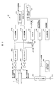
- FIG. 3 is a block diagram of the radiation detection circuit according to the first embodiment.
- the radiation detection circuit 30 according to the present embodiment is installed in the electronic component installation unit 3 shown in FIG. A part of the radiation detection circuit 30 may be installed in the radiation detector stand 1a shown in FIG.
- the radiation detection circuit 30 is, for example, a circuit that corrects the wave height of the radiation detection signal that has been lowered due to recombination of carriers generated in the CdTe element 20 that is a semiconductor element due to the incidence of the radiation 4. In other words, the radiation detection circuit 30 performs a correction process in order to accurately obtain the energy of the incident radiation, for example.
- the carriers are holes and electrons.
- the radiation detection circuit 30 includes a CdTe element 20, capacitors 300a and 300b, preamplifiers 301a and 301b, shaping amplifiers 302a and 302b, peak holds 303a and 303b, and an A / D converter 304a. , 304b, a refresh circuit 305, a refresh control circuit 306, a comparator 307, a correction parameter generation unit 311, and a correction processing unit 312.
- the radiation detection circuit 30 includes at least one of a counter 308, a timer 309, and a temperature measurement unit 31. That is, the radiation detection circuit 30 is configured to include at least one of the counter 308, the timer 309, and the temperature measurement unit 310 based on the dependency of the correction parameter used in the correction formula described later.
- the refresh circuit 305, the refresh control circuit 306, the counter 308, the timer 309, and the temperature measurement unit 310 may be installed in a device other than the radiation detector 2 illustrated in FIG. When these are installed in a device other than the radiation detector 2, parameters such as counter information, refresh elapsed time information, and temperature information described later are input from the outside to the correction parameter generation unit 311 of the radiation detection circuit 30. Become.
- the CdTe element 20 shown in FIG. 3 indicates one pixel among the eight pixels included in one CdTe element 20.
- the CdTe element 20 is sandwiched between the positive electrode 20a and the negative electrode 20b.
- the radiation detector 2 illustrated in FIG. 2 includes, for example, a part or all of the configurations of the radiation detection circuits 30 as many as the number of pixels.
- the capacitor 300a is connected to the positive electrode 20a side, and the capacitor 300b is connected to the negative electrode 20b side.
- the capacitor 300a and the capacitor 300b are coupling capacitors, cut off the DC voltage component, and only the change in the charge generated in the CdTe element 20 is transmitted to the preamplifier 301a and the preamplifier 301b via the capacitor 300a and the capacitor 300b, respectively. To do.
- the preamplifier 301a is connected to a terminal opposite to the terminal on the positive electrode 20a side of the capacitor 300a.
- the preamplifier 301a amplifies the first radiation detection signal output from the positive electrode 20a via the capacitor 300a.
- the preamplifier 301b is connected to a terminal opposite to the terminal on the negative electrode 20b side of the capacitor 300b.
- the preamplifier 301b amplifies the second radiation detection signal output from the negative electrode 20b via the capacitor 300b.
- the outputs from the preamplifier 301a and the preamplifier 301b correspond to the charge collection efficiency described later.
- the shaping amplifier 302a performs waveform shaping and amplification of the amplified signal output from the preamplifier 301a.
- the shaping amplifier 302b performs waveform shaping and amplification of the amplified signal output from the preamplifier 301b.
- the peak hold 303a is configured to output a signal that keeps the maximum value of the wave height of the waveform-shaped signal output from the shaping amplifier 302a constant.
- the peak hold 303b is configured to output a signal that keeps the maximum value of the wave height of the waveform-shaped signal output from the shaping amplifier 302b constant.
- the signal output from the peak hold 303b on the negative electrode 20b side is input to the A / D converter 304b and the comparator 307.
- the signal output from the peak hold 303b is input to the + terminal (positive input terminal), and the threshold value is input to the ⁇ terminal (negative input terminal).
- the comparator 307 When the signal output from the peak hold 303b is larger than the threshold value, the comparator 307 generates a pulse-shaped trigger signal and outputs it to the A / D conversion unit 304a, the A / D conversion unit 304b, and the counter 308. .
- the A / D conversion unit 304a is configured to convert the signal output from the peak hold 303a into a digital signal and output the digital signal. This digital signal is input to the correction processing unit 312.
- the A / D converter 304b is configured to convert the signal output from the peak hold 303b into a digital signal and output it when the trigger signal output from the comparator 307 is input. This digital signal is input to the correction processing unit 312.
- a refresh circuit 305 is provided between the negative electrode of the power source 313 and the negative electrode 20 b of the CdTe element 20.
- the refresh circuit 305 is controlled by a refresh control circuit 306 connected between the refresh circuit 305 and the timer 309.
- the refresh circuit 305 is a circuit for eliminating the polarization of the CdTe element 20, for example.
- Polarization is a phenomenon in which the charge collection efficiency decreases with time.
- semiconductor elements lattice defects, residual impurities, etc. are inherent in the crystal. Due to these defects, deep levels are formed in the semiconductor element, and carriers in the crystal are trapped or emitted. That is, when radiation is incident on the semiconductor element, the generated carriers are trapped or emitted by the trap in the crystal. Accordingly, in the semiconductor element, for example, electrons as carriers stay in the crystal and become a scattering center in the crystal or generate a space charge, thereby preventing the movement of carriers, so that the charge collection efficiency is long. The energy resolution decreases with the decrease. Further, the polarization proceeds faster as the temperature of the semiconductor element increases. Polarization also depends on the applied bias voltage, and progresses faster as the bias voltage is lower. However, the polarization can be eliminated by temporarily stopping the bias voltage applied to the semiconductor element.
- the refresh control circuit 306 measures the elapsed time from the last refresh process, and generates refresh information and outputs it to the refresh circuit 305 when a predetermined time elapses. That is, the refresh control circuit 306 has a clock and is configured to output refresh information at predetermined time intervals.
- the refresh circuit 305 performs a refresh process based on the input refresh information.
- the refresh process is a process for temporarily stopping the bias voltage applied to the semiconductor element.
- the refresh control circuit 306 outputs refresh information to the refresh circuit 305 and also to the timer 309.
- the timer 309 measures the elapsed time from the last refresh process performed based on the input refresh information, generates refresh elapsed time information, and outputs the generated refresh elapsed time information to the correction parameter generation unit 311.
- the counter 308 calculates the radiation count rate (number of times of incidence of radiation per minute) based on the trigger signal output from the comparator 307, and outputs the calculated result to the correction parameter generation unit 311 as counter information. . Polarization proceeds faster as the counting rate increases.
- the temperature measurement unit 310 measures the temperature of the CdTe element 20 and outputs the measurement result to the correction parameter generation unit 311 as temperature information.
- the temperature of the semiconductor element increases, the mobility of electrons and holes decreases. As a result, in particular, the recombination of holes increases and the wave height decreases. Moreover, the progress of polarization is accelerated by the increase in the temperature of the semiconductor element.
- the correction parameter generation unit 311 generates a correction parameter using at least one parameter of counter information, refresh progress information, and temperature information, and outputs the correction parameter to the correction processing unit 312.
- the correction processing unit 312 corrects the wave heights of the signals output from the A / D conversion unit 304a and the A / D conversion unit 304b based on the correction parameter output from the correction parameter generation unit 311.
- an example of correction processing by the correction processing unit 312 will be described.
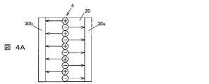
- FIG. 4A is a schematic diagram for explaining electron and hole pair generation due to the incidence of radiation in the semiconductor element according to the first embodiment
- FIG. 4B shows the incident position of the radiation incident on the semiconductor element
- FIG. 4C is a diagram illustrating a relationship between the charge collection efficiency read from the semiconductor element and time.
- a symbol circled with + represents a hole
- a symbol circled with ⁇ represents an electron
- d1 to d5 shown in FIG. 4B indicate positions where the radiation is incident.
- the vertical axis represents charge collection efficiency and the horizontal axis represents time ( ⁇ sec).
- e represents an electron and h represents a hole.
- BP (biparametric) correction which is an example of correction processing, will be described.
- the radiation detection signal is a signal to which holes h contribute almost 100%.
- the rise time of the radiation detection signal until the wave height becomes maximum is long, and some of the holes disappear due to recombination during movement. Therefore, as shown by a two-dot chain line in FIG. 4C, the rise time of the signal is the longest and the wave height is the minimum among the radiation detection signals shown in FIG. 4A.
- the radiation detection signal is a signal to which the electrons e contribute almost 100%. Since electrons have a higher mobility than holes, the rise time of the radiation detection signal is fast, and recombination during movement hardly occurs. Therefore, as shown by a solid line in FIG. 4C, the rising of the signal is fast and the wave height is maximum in the radiation detection signal shown in FIG. 4A.
- time constant is used as a numerical value representing the speed of rising of the signal.
- This “time constant” means the time from the beginning of the signal rise (0 on the horizontal axis in FIG. 4C) to a predetermined time, and when divided in this way, the charge that is the value of the signal at the predetermined time It is a numerical value for comparing the collection efficiency (vertical axis in FIG. 4C).
- the early time is indicated by fast
- the late time is indicated by slow.
- time constant fast or time constant slow means the time from the start of the rise of the above signal to the predetermined time, and also means the time shown in FIG. 4C for convenience. To do.
- the distance to the electrode is the same.
- the signal contributes 50% and hole h almost 50%. Therefore, as shown by dotted lines with long intervals in FIG. 4C, the rise time of the radiation detection signal is approximately in the middle between the incident position d1 and the incident position d5. Therefore, the wave height at the incident position d3 is slightly lower than the wave height at the incident position d5. This is because some of the holes disappear due to recombination.
- the incident position is close to the positive electrode 20a. Is approximately 25% and hole h is approximately 75%. Therefore, as indicated by a one-dot chain line in FIG. 4C, the rising of the signal is approximately in the middle between the incident position d1 and the incident position d3. Accordingly, the wave height at the incident position d2 is lower than the wave height at the incident position d3. This is because the contribution ratio of holes is high and some of the holes disappear due to recombination.
- the incident position is close to the negative electrode 20b. Is approximately 75% and hole h is approximately 25%. Therefore, as shown by a dotted line with a short interval in FIG. 4C, the rising of the signal is approximately in the middle between the incident position d3 and the incident position d5. Therefore, the wave height at the incident position d4 is slightly lower than the wave height at the incident position d5. This is because the contribution ratio of holes is high.
- the wave height at the time constant fast and the wave height at the time constant slow are substantially equal.
- the wave height at the time constant fast is significantly smaller than the wave height at the time constant slow.
- the incident position of the radiation can be estimated by comparing the wave height at the time constant fast with the wave height at the time constant slow. In other words, this comparison makes it possible to estimate the amount of hole recombination, so it is possible to estimate the energy lost due to recombination. Can be obtained with high accuracy.
- the shaping amplifier 302a connected to the positive electrode 20a side has a time constant set so as to output a signal having a wave height at the time constant slow.
- this time constant is referred to as a time constant slow.
- the shaping amplifier 302b connected to the negative electrode 20b side has a time constant set so as to output a wave height signal at the time constant fast. That is, the signal output from the shaping amplifier 302a is a signal processed with a longer time constant than the signal output from the shaping amplifier 302b. In other words, the signal output from the shaping amplifier 302b is a signal processed with a shorter time constant than the signal output from the shaping amplifier 302a.
- this time constant is referred to as a time constant fast.
- the time constant described above may be such that the shaping amplifier 302a on the positive electrode 20a side is fast and the shaping amplifier 302b on the negative electrode 20b side is slow.
- the following formula (1) shows an example of the correction formula used for the above BP correction.
- E A ⁇ H slow (1 + B (H slow ⁇ H fast ) / H slow ) (1)
- E is the wave height after BP correction
- a and B are correction parameters.
- This equation (1) shows that the wave height at the time constant fast (H fast ) is significantly lower than the wave height at the time constant slow (H slow ), that is, when the contribution ratio of holes is high, the wave height at the time constant slow ( It is a correction formula for raising the wave height in proportion to the difference between the wave height (H slow ) and the wave height (H fast ) at the time constant fast.
- FIG. 5A is a graph regarding the temperature dependency of the correction parameter according to the first embodiment
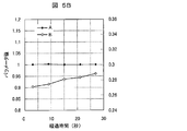
- FIG. 5B is a graph regarding the elapsed time dependency after the correction parameter is refreshed.
- the horizontal axis represents the temperature (° C.) of the CdTe element
- the left vertical axis represents the parameter value of the correction parameter A
- the right vertical axis represents the parameter value of the correction parameter B.
- the horizontal axis represents the elapsed time (seconds) after the refresh
- the left vertical axis is the parameter value of the correction parameter A
- the right vertical axis is the parameter value of the correction parameter B. Note that the temperature dependence of the correction parameter shown in FIG.
- the radiation having the same energy is emitted toward the CdTe element at each temperature, and the wave height after the BP correction processing is estimated from the energy of the radiation.
- the correction parameters are calculated so as to be equal to and illustrated.
- the elapsed time dependency after the refresh process of the correction parameter shown in FIG. 5B is that radiation having the same energy is emitted toward the CdTe element while changing the elapsed time from the end of the refresh process, and after the BP correction process.
- the correction parameter is calculated so that the wave height is equal to the wave height estimated from the energy of the radiation, and is illustrated.
- the correction parameter B is particularly highly temperature-dependent and time-dependent. Therefore, the wave height can be corrected more accurately by changing the correction parameter used for the correction process according to the temperature of the CdTe element and the elapsed time after the end of the refresh process.
- the following formula (2) shows another example of the correction formula used for the BP correction.
- FIG. 6 is a graph showing the temperature dependence of the correction parameter according to the first embodiment.
- the horizontal axis represents the temperature (° C.) of the CdTe element
- the vertical axis represents the parameter value.
- the temperature dependency of the correction parameter shown in FIG. 6 is that radiation having the same energy is emitted toward the CdTe element at each temperature, and the wave height after the BP correction processing is the wave height estimated from the energy of the radiation.
- the correction parameters are calculated so as to be equal and illustrated.
- each parameter value varies with temperature even when the correction formula is the above formula (2) different from the above formula (1). Therefore, the wave height can be corrected more accurately by changing the correction parameters A, B, and C used for the correction process according to the temperature of the CdTe element.
- Various correction formulas other than the correction formulas exemplified above can be considered as the correction formula used for the correction processing. Therefore, whether the counter 308, the timer 309, and the temperature measurement unit 310 are incorporated into the radiation detection circuit 30 is selected based on, for example, the dependency of the correction parameter of the correction formula employed in the correction process.
- the first radiation detection signal output from the positive electrode 20a side is input to the A / D conversion unit 304a via the capacitor 300a, the preamplifier 301a, the shaping amplifier 302a, and the peak hold 303a, and the A / D conversion unit 304a
- the wave height output with the time constant slow is converted into a digital signal and output to the correction processing unit 312.
- the second radiation detection signal output from the negative electrode 20b side is input to the A / D conversion unit 304b via the capacitor 300b, the preamplifier 301b, the shaping amplifier 302b, and the peak hold 303b, and the A / D conversion unit 304b. Converts the wave height output with the time constant fast into a digital signal and outputs the digital signal to the correction processing unit 312.
- the peak hold 303b outputs a signal with a constant wave height to the A / D converter 304b and outputs the signal to the + terminal of the comparator 307.
- the comparator 307 compares the threshold value input to the ⁇ terminal and the signal input to the + terminal, and generates a trigger signal when the wave height of the signal is larger than the threshold value, and the A / D converters 304a, A The data is output to the / D conversion unit 304b and the counter 308.
- the A / D converter 304a and the A / D converter 304b convert the wave height into a digital signal based on the trigger signal.
- the counter 308 counts the trigger signal, generates counter information, and outputs the counter information to the correction parameter generation unit 311.
- the correction parameter generation unit 311 generates a correction parameter based on the counter information, the refresh elapsed time information acquired from the timer 309, and the temperature information of the CdTe element 20 acquired from the temperature measurement unit 310.
- the correction parameter generation unit 311 outputs the generated correction parameter to the correction processing unit 312.
- the correction processing unit 312 performs correction processing so that a wave height corresponding to the energy of the radiation 4 is obtained based on the wave height of the time constant fast, the wave height of the time constant slow, and the correction parameter.
- the correction processing unit 312 outputs the corrected wave height obtained by the correction processing as corrected wave height information.
- the corrected wave height information is output, for example, for each pixel on which the radiation 4 is incident, converted into image information by an external device, and visualized.
- the correction parameter is generated using at least one of the counter information, the refresh progress information, and the temperature information.
- the wave height can be accurately corrected so as to approach the wave height estimated from the energy of the incident radiation. Therefore, since the radiation detector according to the present embodiment can correct the wave height accurately, it can detect the energy of the radiation with high accuracy.
- the radiation detection circuit 30 is the same as those of the first exemplary embodiment, and operations after the shaping amplifier 302a and the shaping amplifier 302b are the same as those of the first exemplary embodiment.
- the radiation detection signal output from the positive electrode 20a is used.
- the present invention is not limited to this, and the radiation detection signal output from the negative electrode 20b may be used.
- the radiation detector 2 according to the second embodiment performs correction processing based on the radiation detection signal output from the positive electrode 20a or the negative electrode 20b, the radiation detection output from the positive electrode 20a and the negative electrode 20b. Compared with the case where a signal is used, the number of parts is reduced, and the manufacturing cost of the radiation detector 2 can be reduced.
- the third embodiment is different from the above-described embodiments in that BP correction is performed using the rising speed (rise time) of the radiation detection signal.
- the comparator 307b compares the signal output from the shaping amplifier 302b input to the + terminal with the first threshold value (low) input to the ⁇ terminal, and the wave height of the signal output from the shaping amplifier 302b is the first.
- the threshold value is larger than 1, a start signal is generated, and the start signal is output to the time measuring unit 314.
- the time measuring unit 314 calculates the rise time shown in FIG. 9 based on the start signal output from the comparator 307b and the stop signal output from the comparator 307c, and generates rise time information.
- the rise time is a time interval (time difference) from when the start signal is input to when the stop signal is input.
- the time measuring unit 314 outputs the generated rise time information to the correction processing unit 312. It can be seen that when the rise time is the shortest, the radiation detection signal contributes almost 100% of the electrons, and when the rise time is the longest, the radiation detection signal contributes almost 100% of the holes.
- the correction processing unit 312 calculates the wave height after BP correction from the rise time, the wave height at the time constant fast or the time constant slow, and the correction parameter.
- the counter 308 of this embodiment counts the incidence of radiation based on the trigger signal output from the comparator 307a.
- the radiation detection signal output from the positive electrode 20a is input to the preamplifier 301a via the capacitor 300a, and the signal amplified by the preamplifier 301a is input to the shaping amplifier 302a and the shaping amplifier 302b.
- the signal input to the shaping amplifier 302a is waveform-shaped, and then output to the A / D converter 304a and the + terminal of the comparator 307a as a signal fixed to the maximum value of the peak height by the peak hold 303a.
- the comparator 307a compares the signal input to the + terminal with the threshold value input to the-terminal, and generates a trigger signal when the input signal is greater than the threshold value, and generates an A / D converter 304a and Output to the counter 308.
- the A / D conversion unit 304a converts the signal output from the peak hold 303a into a digital signal based on the trigger signal and outputs the digital signal to the correction processing unit 312.
- the counter 308 calculates the radiation count rate based on the trigger signal, and outputs the calculated result to the correction parameter generation unit 311 as counter information.
- the signal input to the shaping amplifier 302b is waveform-shaped and input to the + terminal of the comparator 307b and the + terminal of the comparator 307c.
- the comparator 307b compares the signal input to the + terminal with the first threshold value input to the ⁇ terminal, and generates a start signal when the input signal is greater than the first threshold value, Output to the measurement unit 314.
- the comparator 307c compares the signal input to the + terminal with the second threshold value input to the ⁇ terminal, and generates a stop signal when the input signal is greater than the second threshold value. To the time measuring unit 314.
- the time measuring unit 314 measures the time interval between the time when the start signal is input and the time when the stop signal is input, generates rise time information, and outputs the rise time information to the correction processing unit 312.
- the correction parameter generation unit 311 generates a correction parameter based on the counter information, the refresh elapsed time information acquired from the timer 309, and the temperature information of the CdTe element 20 acquired from the temperature measurement unit 310.
- the correction parameter generation unit 311 outputs the generated correction parameter to the correction processing unit 312.
Landscapes
- Physics & Mathematics (AREA)
- Health & Medical Sciences (AREA)
- Life Sciences & Earth Sciences (AREA)
- General Physics & Mathematics (AREA)
- High Energy & Nuclear Physics (AREA)
- Molecular Biology (AREA)
- Spectroscopy & Molecular Physics (AREA)
- Measurement Of Radiation (AREA)
- Solid State Image Pick-Up Elements (AREA)
Abstract
本発明は、陽電極20a及び陰電極20bを有し放射線4の入射に対して放射線検出信号を出力するCdTe素子20(半導体素子)と、補正パラメータ生成部311と、補正処理部312とを備えた放射線検出装置において、補正パラメータ生成部311は、放射線4の入射によりCdTe素子20に生じたキャリアが再結合することによって低下した放射線検出信号の波高を補正する補正処理に用いる補正パラメータを生成し、補正処理部312は、補正パラメータ生成部311で生成された補正パラメータに基づいて補正処理を行うことを特徴とする。本発明によれば、放射線検出信号の波高を補正することができるため、放射線検出装置の検出精度を向上することができる。
Description
本発明は、放射線検出装置に関する。
従来の技術としては、例えば、特許文献1に記載されているように、微分手段と積分手段との組み合わせからなる準ガウス形フィルタを含む波形整形増幅手段と、上記微分手段の出力に関する信号波高と上記波形整形増幅手段の出力信号波高を比較することにより事象ごとの電荷収集時間情報を得る手段と、上記電荷収集時間情報に応じて事象ごとに上記波形整形増幅手段の出力信号波高を補正することにより電荷収集の不完全性に起因するエネルギー分解能の劣化を改善する補正手段とを有する半導体放射線検出装置が知られている。
特許文献1に記載の半導体放射線検出装置によれば、電荷収集の不完全性及び波形整形増幅手段の入力信号の立ち上がりに起因するエネルギー分解能の劣化を、検出効率を低下させずに改善することができるとされている。
特許文献1に記載の半導体放射線検出装置は、出力信号波高の補正に用いるパラメータが固定値であり、検出素子の温度及び分極(ポラリゼーション)等に起因するエネルギー分解能の劣化により、安定して放射線のエネルギーを検出することが困難である。
本発明の目的は、放射線検出装置において、放射線のエネルギーの検出精度を向上することにある。
本発明の放射線検出装置においては、補正パラメータ生成部は、放射線の入射により半導体素子に生じたキャリアが再結合することによって低下した放射線検出信号の波高を補正する補正処理に用いる補正パラメータを生成し、補正処理部は、補正パラメータ生成部で生成された補正パラメータに基づいて補正処理を行うことを特徴とする。
本発明によれば、放射線検出信号の波高を補正することができるため、放射線検出装置の検出精度を向上することができる。
実施の形態に係る放射線検出装置は、陽電極及び陰電極を有し放射線の入射に対して放射線検出信号を出力する半導体素子と、補正パラメータ生成部と、補正処理部とを備え、補正パラメータ生成部は、放射線の入射により半導体素子に生じたキャリアが再結合することによって低下した放射線検出信号の波高を補正する補正処理に用いる補正パラメータを生成し、補正処理部は、補正パラメータ生成部で生成された補正パラメータに基づいて補正処理を行うことを特徴とする。
前記放射線検出装置は、さらに、半導体素子の温度を測定して温度情報を生成する温度測定部、半導体素子のリフレッシュ処理からの経過時間を示すリフレッシュ経過時間情報を生成する経過時間情報生成部、及び半導体素子に入射した放射線の計数率を示すカウント情報を生成するカウント情報生成部の少なくとも1つを備え、補正パラメータ生成部は、温度情報、リフレッシュ経過時間情報及びカウント情報の少なくとも1つに基づいて補正パラメータを生成することが望ましい。
前記放射線検出信号は、陽電極から出力される第1の放射線検出信号、及び陰電極から出力される第2の放射線検出信号とからなり、補正処理部は、第1の放射線検出信号と、第1の放射線検出信号よりも短い時定数で処理された信号(短時定数信号)又は第1の放射線検出信号よりも長い時定数で処理された信号(長時定数信号)である第2の放射線検出信号とに基づいて補正処理を行うことが望ましい。
前記放射線検出装置は、さらに、陽電極又は陰電極から出力された放射線検出信号を2つに分ける回路を設け、補正処理部は、2つに分けた一方の信号である短時定数信号と、この信号(短時定数信号)よりも長時定数信号とに基づいて補正処理を行うことが望ましい。
前記補正処理部は、放射線検出信号が第1のしきい値に達した時間と、第1のしきい値よりも大きい第2のしきい値に達した時間との時間差、及び放射線検出信号に基づいて補正処理を行うことが望ましい。
以下、図面を用いて具体的に説明する。
[第1の実施の形態]
(放射線検出装置の構成の概要)
図1は、第1の実施の形態に係る放射線検出装置の斜視図である。
(放射線検出装置の構成の概要)
図1は、第1の実施の形態に係る放射線検出装置の斜視図である。
本図において、放射線検出装置1は、複数の放射線検出器2を平面的に(二次元的に)並べた構成である。放射線検出器2は、放射線検出器立て1aによって保持されている。放射線検出器立て1aは、基部10と、この基部10の上に設置された複数の支持体11と、複数のコネクタ12とで構成されている。コネクタ12は、基部10と支持体11との間に配置されている。支持体11には、定められた間隔で複数の溝111が形成されている。これらの溝111には、複数の放射線検出器2が挿入され、固定されている。
支持体11は、基部10の上に放射線検出器2の幅に対応する間隔を有して設けられている。そして、複数の支持体11はそれぞれ、複数の壁部110を有しており、隣り合う壁部110の間に溝111が形成されている。壁部110は、一方の表面にくぼみ部112が設けられ、他方の表面は平坦面113である。
(放射線検出器の構成)
図2は、図1の放射線検出器2を拡大して示した斜視図である。
図2は、図1の放射線検出器2を拡大して示した斜視図である。
本図において、放射線検出器2は、半導体素子であるCdTe素子20、CdTe素子20を接続した基板21、フレキシブル基板22、及びカードエッジ部224を有している。放射線検出器2のカードエッジ部224は、図1に示す放射線検出器立て1aのコネクタ12によって接続されるようになっている。
放射線検出器2の弾性部材実装部250には、例えば、板金を用いて形成される弾性部材251が組み込まれている。図2に示す支持体11の溝111に放射線検出器2が挿入されると、放射線検出器2は、弾性部材251によって壁部110の平坦面113に押し付けられ、支持体11に放射線検出器2が固定される。なお、複数の支持体11はそれぞれ金属材料から切削等により形成したものである。
放射線検出器2は、γ線、X線等の放射線4を検出する放射線検出器である。図2において放射線4は、放射線検出器2の半導体素子としてのCdTe素子20からカードホルダ23に向かう方向(図中の矢印の方向)に沿って伝搬して放射線検出器2に入射する。
放射線4は、CdTe素子20の入射面(図2においては、すべてのCdTe素子20が接する平面(側面))に入射する。このように半導体素子の側面を放射線4の入射面とする放射線検出器を、エッジオン型の放射線検出器と称する。
なお、放射線検出器2は、特定の方向(例えば、被検体から放射線検出器2に向かう方向)に沿って入射してくる放射線4が通過する複数の開口を有するコリメータを介して放射線4を検出する。なお、コリメータは、多孔平行コリメータであるが、これに限定されず、ピンホールコリメータ等を用いても良い。また、本実施の形態は、エッジオン型でない放射線検出器にも適用することができる。また、本実施の形態に係る放射線検出器2は、カード型の形状を呈する。
また、放射線検出器2の基板21は、カードホルダ23とカードホルダ24とに挟み込まれて支持されている。カードホルダ23とカードホルダ24とはそれぞれ、同一形状を有する。カードホルダ23には溝付穴230が設けてあり、カードホルダ24の突起部240が嵌め合わされている。カードホルダ24にも溝付穴(図示しない)が設けてあり、カードホルダ23の突起部231が嵌め合わされている。これにより、基板21はカードホルダ23、24に固定されている。
また、弾性部材実装部250は、放射線検出器立て1aに放射線検出器2が挿入される際、放射線検出器2を図2に示す放射線検出器立て1aに押し付けて固定する弾性部材251が設けられる部分である。なお、放射線検出器立て1aは、カードエッジ部224が挿入されるコネクタ12を有しており、カードエッジ部224がコネクタ12に挿入されると、放射線検出器2は、カードエッジ部224に形成されたパターン225とコネクタ12とが電気的に接続される。これにより、放射線検出器2は、外部の制御回路、外部からの電源線、グランド線等に電気的に接続される。
図2においては、例として、放射線検出器2は、基板21の両側にそれぞれ4個のCdTe素子20が一定の間隔で配置されている。
フレキシブル基板22は、フィルム状の樹脂(例えば、ポリイミド)を用いて形成された基板である。
図2に示すフレキシブル基板22は、略半円形状の接続部220、221、222、223を有する。接続部220、221、222、223は、導電性材料を用いて形成されたパターンであり、例えば、Cu等を用いて形成される。接続部220は、基板端子210と電気的に接続するように構成されている。同様に、接続部221は基板端子211と、接続部222は基板端子212と、接続部223は基板端子213と、それぞれ、電気的に接続されている。なお、図2においては、CdTe素子20は基板21に対して対称に配置されており、図中、フレキシブル基板22の裏側に配置されたフレキシブル基板、及びこれと電気的に接続された基板端子も設置されているが、図示は省略している。
また、図示していないが、CdTe素子20は、表面に略等間隔で設けられた複数の溝部を有する。本実施の形態においては、CdTe素子20は、7本の溝部を有する。
これらの溝部で分けられるCdTe素子20の部分のそれぞれは、放射線4を検出する1個の画素(ピクセル)に対応する。これにより、1個のCdTe素子20は、複数の画素を有することになる。よって、1個の放射線検出器2が8個のCdTe素子20を備え、1個のCdTe素子20が8個のピクセルを有する場合、1個の放射線検出器2は、64ピクセルの解像度を有することになる。溝部の数を増減させることにより、1個のCdTe素子20のピクセル数を増減させることができる。
基板21は、複数のCdTe素子20のそれぞれが設置される第1の端部側の幅が、複数のCdTe素子20が設置される第1の端部側の反対側の第2の端部側よりも広く形成される。なお、第2の端部側において基板21は、カードホルダ23及びカードホルダ24によって支持される。また、第2の端部側には、放射線検出器2と外部の制御回路とを電気的に接続可能とする複数のパターン225が設けられたカードエッジ部224が設けられる。また、CdTe素子20と電気的に接続する基板21に形成された素子接続部(図示せず)とカードエッジ部224との間には、素子接続部を介して複数のCdTe素子20のそれぞれと電気的に接続される抵抗、コンデンサ等の電子部品を設置する複数の電子部品設置部3が設けられる。なお、電子部品設置部3には、後述するApplication Specific Integrated Circuit(ASIC)、Field Programmable Gate Array(FPGA)等が設置される。
なお、基板21は、一例として、幅広の方向、すなわち長手方向は40mm程度の長さとしてある。そして、基板21は、幅広の部分の端部から幅が狭くなっている部分の端部まで、すなわち、素子接続部が設けられている部分の端からカードエッジ部224の端までの短手方向は、20mm程度の長さとしてある。
本実施の形態において、半導体素子を構成する化合物半導体としては、例としてCdTeを用いたが、これに限定されるものではなく、γ線等の放射線を検出するCdZnTe(CZT)素子、HgI2素子等の化合物半導体素子を用いることもできる。
(放射線検出回路の構成)
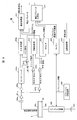
図3は、第1の実施の形態に係る放射線検出回路のブロック図である。
図3は、第1の実施の形態に係る放射線検出回路のブロック図である。
本実施の形態に係る放射線検出回路30は、図2に示す電子部品設置部3に設置される。放射線検出回路30の一部は、図1に示す放射線検出器立て1aに設置されるようにしてもよい。
放射線検出回路30は、例えば、放射線4の入射によって半導体素子であるCdTe素子20に生じたキャリアが再結合することにより低下した放射線検出信号の波高を補正する回路である。つまり、放射線検出回路30は、例えば、入射した放射線のエネルギーを正確に求めるために補正処理を行う。ここで、キャリアは、正孔及び電子である。
放射線検出回路30は、図3に示すように、CdTe素子20と、コンデンサ300a、300bと、プリアンプ301a、301bと、シェーピングアンプ302a、302bと、ピークホールド303a、303bと、A/D変換部304a、304bと、リフレッシュ回路305と、リフレッシュ制御回路306と、コンパレータ307と、補正パラメータ生成部311と、補正処理部312と、を備えて概略構成されている。
また、放射線検出回路30は、カウンタ308、タイマー309及び温度測定部31の少なくとも1つを備えている。つまり、放射線検出回路30は、後述する補正式に用いる補正パラメータの依存性に基づいてカウンタ308、タイマー309及び温度測定部310の少なくとも1つを備えるように構成される。また、リフレッシュ回路305、リフレッシュ制御回路306、カウンタ308、タイマー309及び温度測定部310は、図2に示す放射線検出器2以外の機器に設置されていても良い。これらが放射線検出器2以外の機器に設置される場合、後述するカウンタ情報、リフレッシュ経過時間情報、温度情報等のパラメータは、外部から放射線検出回路30の補正パラメータ生成部311に入力される構成となる。
図3に示すCdTe素子20は、1つのCdTe素子20が有する8つのピクセルのうちの1つのピクセルを示している。CdTe素子20は、陽電極20aと陰電極20bとに挟まれている。なお、図2に示す放射線検出器2は、例えば、ピクセルの数と同じ数の放射線検出回路30の一部の構成又は全ての構成を備える。
コンデンサ300aは、陽電極20a側に接続され、コンデンサ300bは、陰電極20b側に接続されている。このコンデンサ300a及びコンデンサ300bは、カップリングコンデンサであり、直流電圧成分を遮断し、CdTe素子20に生じた電荷の変化分のみがこのコンデンサ300a及びコンデンサ300bを介してプリアンプ301a及びプリアンプ301bにそれぞれ伝達する。
プリアンプ301aは、コンデンサ300aの陽電極20a側の端子と反対の端子に接続されている。このプリアンプ301aは、コンデンサ300aを介して陽電極20aから出力された第1の放射線検出信号を増幅する。
プリアンプ301bは、コンデンサ300bの陰電極20b側の端子と反対の端子に接続されている。このプリアンプ301bは、コンデンサ300bを介して陰電極20bから出力された第2の放射線検出信号を増幅する。なお、プリアンプ301a及びプリアンプ301bからの出力は、後述の電荷収集効率に対応するものである。
シェーピングアンプ302aは、プリアンプ301aから出力された増幅信号の波形整形及び増幅を行う。
シェーピングアンプ302bは、プリアンプ301bから出力された増幅信号の波形整形及び増幅を行う。
ピークホールド303aは、シェーピングアンプ302aから出力された波形整形後の信号の波高の最大値を一定に保持する信号を出力するように構成されている。
ピークホールド303bは、シェーピングアンプ302bから出力された波形整形後の信号の波高の最大値を一定に保持する信号を出力するように構成されている。この陰電極20b側のピークホールド303bから出力された信号は、A/D変換部304bとコンパレータ307に入力する。
ここで、コンパレータ307は、+端子(正入力端子)にピークホールド303bから出力された信号が入力し、-端子(負入力端子)にしきい値が入力する。コンパレータ307は、ピークホールド303bから出力された信号が、しきい値よりも大きいとき、パルス形状のトリガ信号を生成し、A/D変換部304a、A/D変換部304b及びカウンタ308に出力する。
A/D変換部304aは、コンパレータ307から出力されたトリガ信号が入力すると、ピークホールド303aから出力された信号をデジタル信号に変換して出力するように構成されている。このデジタル信号は、補正処理部312に入力する。
A/D変換部304bは、コンパレータ307から出力されたトリガ信号が入力すると、ピークホールド303bから出力された信号をデジタル信号に変換して出力するように構成されている。このデジタル信号は、補正処理部312に入力する。
ここで、電源313の負電極とCdTe素子20の陰電極20bとの間には、リフレッシュ回路305が設けられている。このリフレッシュ回路305は、リフレッシュ回路305とタイマー309との間に接続されたリフレッシュ制御回路306により制御される。このリフレッシュ回路305は、例えば、CdTe素子20のポラリゼーション解消のための回路である。
ポラリゼーションとは、電荷収集効率が時間と共に減少する現象である。半導体素子には、その結晶中に格子欠陥や残留不純物等が内在する。これらの欠陥により、半導体素子には、深い準位が形成され、結晶中のキャリアが捕捉されたり、放出されたりする。つまり、半導体素子に放射線が入射すると、発生したキャリアが結晶内のトラップに捕捉されたり、放出されたりする。従って、半導体素子は、例えば、キャリアとしての電子が結晶内に留まり、結晶内での散乱中心となったり、空間電荷を発生させたりすることで、キャリアの移動を妨げるので、電荷収集効率が時間と共に減少し、エネルギー分解能が劣化する。また、ポラリゼーションは、半導体素子の温度が高くなるほど、進行が速くなる。また、ポラリゼーションは、印加されるバイアス電圧にも依存し、バイアス電圧が低いほど進行が速くなる。しかし、ポラリゼーションは、半導体素子に印加するバイアス電圧を一時的に停止することにより、解消できる。
そこで、リフレッシュ制御回路306は、最後にリフレッシュ処理を行った時間からの経過時間を計測し、予め定められた時間が経過すると、リフレッシュ情報を生成し、リフレッシュ回路305に出力する。つまり、リフレッシュ制御回路306は、クロックを有し、予め定められた時間間隔でリフレッシュ情報を出力するように構成されている。リフレッシュ回路305は、入力したリフレッシュ情報に基づいてリフレッシュ処理を行う。このリフレッシュ処理とは、半導体素子に印加するバイアス電圧を一時的に停止する処理である。
また、リフレッシュ制御回路306は、リフレッシュ情報をリフレッシュ回路305に出力すると共に、タイマー309にも出力する。タイマー309は、入力したリフレッシュ情報に基づいて最後の行われたリフレッシュ処理からの経過時間を計測してリフレッシュ経過時間情報を生成し、生成したリフレッシュ経過時間情報を補正パラメータ生成部311に出力する。
カウンタ308は、例えば、コンパレータ307から出力されるトリガ信号に基づいて放射線の計数率(1分間当たりの放射線の入射回数)を算出し、算出した結果をカウンタ情報として補正パラメータ生成部311に出力する。ポラリゼーションは、計数率の増加に応じて進行が速くなる。
温度測定部310は、CdTe素子20の温度を測定し、測定した結果を温度情報として補正パラメータ生成部311に出力する。半導体素子の温度が高くなると、電子及び正孔の移動度が低下する。その結果、特に、正孔の再結合が増加し、波高が低下する。また、半導体素子の温度が高くなることで、ポラリゼーションの進行が速くなる。
補正パラメータ生成部311は、カウンタ情報、リフレッシュ経過情報及び温度情報の少なくとも1つのパラメータを用いて補正パラメータを生成し、補正処理部312に出力する。
補正処理部312は、補正パラメータ生成部311から出力された補正パラメータに基づいてA/D変換部304a及びA/D変換部304bから出力された信号の波高を補正する。以下に、補正処理部312による補正処理の一例について説明する。
(補正処理について)
図4Aは、第1の実施の形態に係る半導体素子における放射線の入射による電子及び正孔の対生成を説明するための概略図であり、図4Bは、半導体素子に入射した放射線の入射位置を示す概略図であり、図4Cは、半導体素子から読み出される電荷収集効率と時間との関係を示す図である。
図4Aは、第1の実施の形態に係る半導体素子における放射線の入射による電子及び正孔の対生成を説明するための概略図であり、図4Bは、半導体素子に入射した放射線の入射位置を示す概略図であり、図4Cは、半導体素子から読み出される電荷収集効率と時間との関係を示す図である。
図4Aにおいて+を丸で囲った記号は正孔を表し、-を丸で囲った記号は電子を表す。また、図4Bに示すd1~d5は、放射線が入射した位置を示すものである。
図4Cにおいて縦軸は電荷収集効率(Charge Collection Efficiency)であり、横軸は時間(μsec)である。また、図4Cにおいてeは電子を表し、hは正孔を表す。図4Cにおいて「e:h」は電子及び正孔の寄与率を表す。例えば、「e:h=100:0」は、放射線検出により出力される放射線検出信号の生成に、電子が100%、正孔が0%寄与していることを示している。
以下では、補正処理の一例であるBP(バイパラメトリック)補正について説明する。
図4Aに示すように、放射線4がCdTe素子20に入射して相互作用(光電効果、コンプトン散乱又は電子対生成)を生じることにより、CdTe素子20内の原子が電離し、電子及び正孔のペアが発生する。このペアの数は、入射する放射線4のエネルギーに比例するため、これを正確に読み出すことが優れたエネルギー決定精度(エネルギー分解能)に繋がる。
CdTe素子20に発生した電子及び正孔は、ただCdTe素子20に入射しただけの場合、再結合して消滅する。そこで、CdTe素子20の陽電極20a及び陰電極20b間に高電圧(例えば、600V)のバイアス電圧を印加して電極間に電場を発生させることで、図4Aに示すように、電子は陽電極20aに向けて移動し、正孔は陰電極20bに向けて移動する。放射線検出器2は、この移動を信号として読み出すものである。
放射線4が、図4Bに示すように、陽電極20aに最も近い入射位置d1に入射したとき、入射位置d1で電子及び正孔が対生成し、電子は陽電極20aに向けて移動し、正孔は陰電極20bに向けて移動する。電子は、すぐに陽電極20aに到達するため、誘起電荷は、主に、正孔の移動により生じる。つまり、放射線検出信号は、正孔hがほぼ100%寄与する信号となる。しかし、正孔は、電子に比べて移動度が低いため、波高が最大となるまでの放射線検出信号の立ち上がり時間は長くなり、また、移動中の再結合により正孔の一部が消滅する。従って、図4Cに二点鎖線で示すように、図4Aに示す放射線検出信号の中で、信号の立ち上がり時間が最も長く、波高が最小となる。
放射線4が、図4Bに示すように、陰電極20bに最も近い入射位置d5に入射したとき、入射位置d5で電子及び正孔が対生成する。正孔は、すぐに陰電極20bに到達するため、誘起電荷は、主に、電子の移動により生じる。つまり、放射線検出信号は、電子eがほぼ100%寄与する信号となる。電子は、正孔に比べて移動度が高いため、放射線検出信号の立ち上がり時間は早くなり、また、移動中の再結合はほとんど生じない。従って、図4Cに実線で示すように、図4Aに示す放射線検出信号の中で、信号の立ち上がりが早く、波高が最大となる。なお、以下では、信号の立ち上がりの早さを表す数値として「時定数」を用いることにする。この「時定数」は、信号の立ち上がりの始まり(図4Cにおける横軸の0)から所定の時刻までの時間を意味し、このように区切った場合に当該所定の時刻における信号の値である電荷収集効率(図4Cにおける縦軸)を比較するための数値である。図4Cにおいては、早い時刻をfastで示し、遅い時刻をslowで示してある。以下の記載において、「時定数fast」又は「時定数slow」という場合は、上記の信号の立ち上がりの始まりから当該所定の時刻までの時間を意味するとともに、便宜上、図4Cに示す時刻をも意味する。
放射線4が、図4Bに示すように、陽電極20aと陰電極20bとの中間の入射位置d3に入射したとき、電極までの距離が同じであることから、放射線検出信号は、電子eがほぼ50%、正孔hがほぼ50%寄与する信号となる。よって、図4Cに間隔の長い点線で示すように、放射線検出信号の立ち上がり時間は、入射位置d1と入射位置d5とのおよそ中間となる。従って、入射位置d3の波高は、入射位置d5の波高よりも少し低くなる。これは、正孔の一部が再結合により消滅するからである。
また、放射線4が、図4Bに示すように、入射位置d1と入射位置d3との中間の入射位置d2に入射したとき、入射位置が陽電極20aに近いことから、放射線検出信号は、電子eがほぼ25%、正孔hがほぼ75%寄与する信号となる。よって、図4Cに一点鎖線で示すように、信号の立ち上がりが、入射位置d1と入射位置d3とのおよそ中間となる。従って、入射位置d2の波高は、入射位置d3の波高よりも低くなる。これは、正孔の寄与率が高く、正孔の一部が再結合により消滅するからである。
さらに、放射線4が、図4Bに示すように、入射位置d3と入射位置d5との中間の入射位置d4に入射したとき、入射位置が陰電極20bに近いことから、放射線検出信号は、電子eがほぼ75%、正孔hがほぼ25%寄与する信号となる。よって、図4Cに間隔の短い点線で示すように、信号の立ち上がりが、入射位置d3と入射位置d5とのおよそ中間となる。従って、入射位置d4の波高は、入射位置d5の波高よりも少し低くなる。これは、正孔の寄与率が高いからである。
ここで、図4Cに示すように、電子eがほぼ100%寄与する放射線検出信号においては、時定数fastにおける波高と時定数slowにおける波高とは、ほぼ等しくなる。一方、正孔hがほぼ100%寄与する放射線検出信号においては、時定数fastにおける波高は、時定数slowにおける波高よりも著しく小さい。
従って、時定数slowと時定数fastとの波高に強い相関があるので、放射線の入射位置は、時定数fastにおける波高と時定数slowにおける波高とを比較することによって推定することができる。つまり、この比較により、正孔の再結合の量を推定することができるので、再結合により失ったエネルギーを見積もることが可能となり、この失ったエネルギーを補正処理によって加算し、入射した放射線のエネルギーを精度良く求めることができる。
なお、陽電極20a側に接続されたシェーピングアンプ302aは、時定数slowにおける波高の信号を出力するように時定数が設定されている。以下では、この時定数を時定数slowと記すものとする。また、陰電極20b側に接続されたシェーピングアンプ302bは、時定数fastにおける波高の信号を出力するように時定数が設定されている。つまり、シェーピングアンプ302aから出力される信号は、シェーピングアンプ302bから出力された信号よりも長い時定数で処理された信号である。また、言い換えるならば、シェーピングアンプ302bから出力される信号は、シェーピングアンプ302aから出力された信号よりも短い時定数で処理された信号である。以下では、この時定数を時定数fastと記すものとする。なお、上記の時定数は、陽電極20a側のシェーピングアンプ302aがfast、陰電極20b側のシェーピングアンプ302bがslowであっても良い。
上記のBP補正に用いる補正式の一例を示したものが下記式(1)である。
E=A・Hslow(1+B(Hslow-Hfast)/Hslow) …(1)
ここで、Eは、BP補正後の波高であり、A及びBは、補正パラメータである。この式(1)は、時定数fastにおける波高(Hfast)が、時定数slowにおける波高(Hslow)よりも著しく低い、つまり、正孔の寄与率が高い場合に、時定数slowにおける波高(Hslow)と時定数fastにおける波高(Hfast)との差に比例して波高を嵩上げする補正式である。
ここで、Eは、BP補正後の波高であり、A及びBは、補正パラメータである。この式(1)は、時定数fastにおける波高(Hfast)が、時定数slowにおける波高(Hslow)よりも著しく低い、つまり、正孔の寄与率が高い場合に、時定数slowにおける波高(Hslow)と時定数fastにおける波高(Hfast)との差に比例して波高を嵩上げする補正式である。
図5Aは、第1の実施の形態に係る補正パラメータの温度依存性に関するグラフであり、図5Bは、補正パラメータのリフレッシュ後の経過時間依存性に関するグラフである。図5Aは、横軸がCdTe素子の温度(℃)であり、左側の縦軸が補正パラメータAのパラメータ値であり、右側の縦軸が補正パラメータBのパラメータ値である。また、図5Bは、横軸がリフレッシュ後の経過時間(秒)であり、左側の縦軸が補正パラメータAのパラメータ値であり、右側の縦軸が補正パラメータBのパラメータ値である。なお、図5Aに示す補正パラメータの温度依存性は、同一のエネルギーを有する放射線を、それぞれの温度においてCdTe素子に向けて射出し、BP補正処理後の波高が、放射線のエネルギーから推定される波高と等しくなるように補正パラメータを算出し、図示したものである。また、図5Bに示す補正パラメータのリフレッシュ処理後の経過時間依存性は、同一のエネルギーを有する放射線を、リフレッシュ処理終了からの経過時間を変えてCdTe素子に向けて射出し、BP補正処理後の波高が、放射線のエネルギーから推定される波高と等しくなるように補正パラメータを算出し、図示したものである。
図5A及び5Bに示すように、特に、補正パラメータBが温度依存性及び経過時間依存性が高いことが分かる。従って、CdTe素子の温度、及びリフレッシュ処理終了後からの経過時間によって、補正処理に用いる補正パラメータを変更することにより、より正確に波高を補正することができる。
BP補正に用いる補正式の他の一例を示したものが下記式(2)である。
E=A(B・Hslow-Hfast+C・Hfast
2)/Hslow) …(2)
図6は、第1の実施の形態に係る補正パラメータの温度依存性を示すグラフである。図6は、横軸がCdTe素子の温度(℃)であり、縦軸がパラメータ値である。この図6に示す補正パラメータの温度依存性は、同一のエネルギーを有する放射線を、それぞれの温度においてCdTe素子に向けて射出し、BP補正処理後の波高が、放射線のエネルギーから推定される波高と等しくなるように補正パラメータを算出し、図示したものである。
図6は、第1の実施の形態に係る補正パラメータの温度依存性を示すグラフである。図6は、横軸がCdTe素子の温度(℃)であり、縦軸がパラメータ値である。この図6に示す補正パラメータの温度依存性は、同一のエネルギーを有する放射線を、それぞれの温度においてCdTe素子に向けて射出し、BP補正処理後の波高が、放射線のエネルギーから推定される波高と等しくなるように補正パラメータを算出し、図示したものである。
図6に示すように、補正式が、上記式(1)と異なる上記式(2)であっても、各パラメータ値が温度によって変化することが分かる。従って、CdTe素子の温度によって、補正処理に用いる補正パラメータA、B及びCを変更することにより、より正確に波高を補正することができる。なお、補正処理に用いる補正式は、上記に例示した補正式以外にも様々な式が考えられる。従って、カウンタ308、タイマー309及び温度測定部310は、例えば、補正処理に採用する補正式の補正パラメータの依存性に基づいて放射線検出回路30に組み込まれるか否かが選択される。
以下に、本実施の形態に係る放射線検出器の動作について説明する。
(第1の実施の形態の動作)
図3において、放射線4が放射線検出器2のCdTe素子20に入射すると、入射位置に応じた放射線検出信号が出力される。
図3において、放射線4が放射線検出器2のCdTe素子20に入射すると、入射位置に応じた放射線検出信号が出力される。
陽電極20a側から出力された第1の放射線検出信号は、コンデンサ300a、プリアンプ301a、シェーピングアンプ302a及びピークホールド303aを介してA/D変換部304aに入力され、A/D変換部304aは、時定数slowで出力された波高をデジタル信号に変換して補正処理部312に出力する。
一方、陰電極20b側から出力された第2の放射線検出信号は、コンデンサ300b、プリアンプ301b、シェーピングアンプ302b及びピークホールド303bを介してA/D変換部304bに入力され、A/D変換部304bは、時定数fastで出力された波高をデジタル信号に変換して補正処理部312に出力する。また、ピークホールド303bは、A/D変換部304bに波高が一定となる信号を出力すると共に、コンパレータ307の+端子に当該信号を出力する。コンパレータ307は、-端子に入力するしきい値と+端子に入力する信号とを比較し、しきい値よりも信号の波高が大きいとき、トリガ信号を生成し、A/D変換部304a、A/D変換部304b及びカウンタ308に出力する。A/D変換部304a及びA/D変換部304bは、このトリガ信号に基づいて波高をデジタル信号に変換する。
カウンタ308は、トリガ信号をカウントし、カウンタ情報を生成し、補正パラメータ生成部311に出力する。
補正パラメータ生成部311は、カウンタ情報、タイマー309から取得したリフレッシュ経過時間情報、及び温度測定部310から取得したCdTe素子20の温度情報に基づいて補正パラメータを生成する。補正パラメータ生成部311は、生成した補正パラメータを補正処理部312に出力する。
補正処理部312は、時定数fastの波高、時定数slowの波高、及び補正パラメータに基づいて、放射線4のエネルギーに応じた波高が得られるように、補正処理を行う。補正処理部312は、補正処理によって得られた補正後の波高を、補正波高情報として出力する。この補正波高情報は、例えば、放射線4が入射するピクセルごとに出力され、外部装置により画像情報に変換され視覚化される。
(第1の実施の形態の効果)
第1の実施の形態に係る放射線検出器によれば、カウンタ情報、リフレッシュ経過情報及び温度情報のうち、少なくとも1つを用いて補正パラメータを生成するので、補正パラメータが固定値である場合と比べて、入射した放射線のエネルギーから推定される波高に近づくように、正確に波高を補正することができる。よって、本実施の形態に係る放射線検出器は、正確に波高を補正することができるので、放射線のエネルギーを精度良く検出することができる。
第1の実施の形態に係る放射線検出器によれば、カウンタ情報、リフレッシュ経過情報及び温度情報のうち、少なくとも1つを用いて補正パラメータを生成するので、補正パラメータが固定値である場合と比べて、入射した放射線のエネルギーから推定される波高に近づくように、正確に波高を補正することができる。よって、本実施の形態に係る放射線検出器は、正確に波高を補正することができるので、放射線のエネルギーを精度良く検出することができる。
[第2の実施の形態]
第2の実施の形態は、陽電極側から出力される放射線検出信号から時定数fast及び時定数slowにおける波高を生成する点で第1の実施の形態と異なっている。なお、以下に示す各実施の形態において、第1の実施の形態と同じ機能及び構成を有する部分については、第1の実施の形態と同じ符号を付し、その説明は、省略するものとする。
第2の実施の形態は、陽電極側から出力される放射線検出信号から時定数fast及び時定数slowにおける波高を生成する点で第1の実施の形態と異なっている。なお、以下に示す各実施の形態において、第1の実施の形態と同じ機能及び構成を有する部分については、第1の実施の形態と同じ符号を付し、その説明は、省略するものとする。
(放射線検出回路の構成)
図7は、第2の実施の形態に係る放射線検出回路のブロック図である。以下では、第1の実施の形態と異なっている部分を主に説明する。
図7は、第2の実施の形態に係る放射線検出回路のブロック図である。以下では、第1の実施の形態と異なっている部分を主に説明する。
本実施の形態に係る放射線検出回路30は、図7に示すように、コンデンサ300a及びプリアンプ301aを介して陽電極20aから出力された放射線検出信号を2つに分け、一方は短時定数信号としてシェーピングアンプ302aに出力し、他方は短時定数信号よりも長い時定数で処理された長時定数信号としてシェーピングアンプ302bに出力するように構成されている。
本実施の形態に係る放射線検出回路30の他の構成は、第1の実施の形態と同じであり、シェーピングアンプ302a及びシェーピングアンプ302b以降の動作は、第1の実施の形態と同一である。なお、本実施の形態では、陽電極20aから出力される放射線検出信号を用いたが、これに限定されず、陰電極20bから出力される放射線検出信号を用いても良い。
(第2の実施の形態の効果)
第2の実施の形態に係る放射線検出器2は、陽電極20a又は陰電極20bから出力される放射線検出信号に基づいて補正処理を行うので、陽電極20a及び陰電極20bから出力される放射線検出信号を用いる場合と比べて、部品点数が削減され、放射線検出器2の製造コストを削減することができる。
第2の実施の形態に係る放射線検出器2は、陽電極20a又は陰電極20bから出力される放射線検出信号に基づいて補正処理を行うので、陽電極20a及び陰電極20bから出力される放射線検出信号を用いる場合と比べて、部品点数が削減され、放射線検出器2の製造コストを削減することができる。
[第3の実施の形態]
第3の実施の形態は、放射線検出信号の立ち上がりの早さ(ライズタイム)を用いてBP補正を行う点で上記の各実施の形態と異なっている。
第3の実施の形態は、放射線検出信号の立ち上がりの早さ(ライズタイム)を用いてBP補正を行う点で上記の各実施の形態と異なっている。
(放射線検出回路の構成)
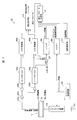
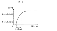
図8は、第3の実施の形態に係る放射線検出回路のブロック図である。図9は、第3の実施の形態に係る補正処理に用いるライズタイムとしきい値との関係を示すグラフである。図9は、縦軸がしきい値であり、横軸が時間(μsec)である。
図8は、第3の実施の形態に係る放射線検出回路のブロック図である。図9は、第3の実施の形態に係る補正処理に用いるライズタイムとしきい値との関係を示すグラフである。図9は、縦軸がしきい値であり、横軸が時間(μsec)である。
図8に示すように、本実施の形態に係る放射線検出回路30は、主に、コンデンサ300a及びプリアンプ301aを介して陽電極20aから出力された放射線検出信号を2つに分け、一方は短時定数信号としてシェーピングアンプ302aに出力し、他方は短時定数信号よりも長い時定数で処理された長時定数信号としてシェーピングアンプ302bに出力するように構成されている。この点は、第2の実施の形態と同様である。また、シェーピングアンプ302bから出力された信号は、コンパレータ307aの+端子及びコンパレータ307bの+端子に出力するように構成されている。なお、本実施の形態では、陽電極20aから出力される放射線検出信号を用いたが、これに限定されず、陰電極20bから出力される放射線検出信号を用いても良い。
シェーピングアンプ302aは、例えば、時定数がfast又はslowでも良く、本実施の形態における時定数は、fastであるものとする。
コンパレータ307aは、+端子に入力するピークホールド303aから出力された信号と、-端子に入力するしきい値とを比較し、ピークホールド303aから出力された信号の波高がしきい値よりも大きいときトリガ信号を生成し、A/D変換部304a及びカウンタ308に出力する。
コンパレータ307bは、+端子に入力するシェーピングアンプ302bから出力された信号と、-端子に入力する第1のしきい値(低)とを比較し、シェーピングアンプ302bから出力された信号の波高が第1のしきい値よりも大きいときスタート信号を生成し、時間測定部314にスタート信号を出力する。
コンパレータ307cは、+端子に入力するシェーピングアンプ302bから出力された信号と、-端子に入力する第2のしきい値(高)とを比較し、シェーピングアンプ302bから出力された信号の波高が第2のしきい値よりも大きいときストップ信号を生成し、時間測定部314にストップ信号を出力する。なお、第1のしきい値(低)は、第2のしきい値(高)よりも小さい。
時間測定部314は、コンパレータ307bから出力されたスタート信号と、コンパレータ307cから出力されたストップ信号とに基づいて図9に示すライズタイムを算出し、ライズタイム情報を生成する。このライズタイムは、スタート信号が入力してからストップ信号が入力するまでの時間間隔(時間差)である。
時間測定部314は、生成したライズタイム情報を補正処理部312に出力する。このライズタイムが最も短いとき、電子がほぼ100%寄与した放射線検出信号であることが分かり、最も長いとき、正孔がほぼ100%寄与した放射線検出信号であることが分かる。補正処理部312は、このライズタイムと、時定数fast又は時定数slowにおける波高、及び補正パラメータとからBP補正後の波高を算出する。
本実施のカウンタ308は、コンパレータ307aから出力されたトリガ信号に基づいて放射線の入射をカウントする。
(第3の実施の形態の動作)
放射線4が、放射線検出器2のCdTe素子20に入射すると、入射位置に応じた放射線検出信号が陽電極20a側から出力される。
放射線4が、放射線検出器2のCdTe素子20に入射すると、入射位置に応じた放射線検出信号が陽電極20a側から出力される。
陽電極20aから出力された放射線検出信号は、コンデンサ300aを介してプリアンプ301aに入力し、プリアンプ301aによって増幅された信号がシェーピングアンプ302a及びシェーピングアンプ302bに入力する。
シェーピングアンプ302aに入力した信号は、波形整形された後、ピークホールド303aによって波高の最大値に固定された信号としてA/D変換部304a、及びコンパレータ307aの+端子に出力される。
コンパレータ307aは、+端子に入力した信号と、-端子に入力したしきい値とを比較し、入力した信号がしきい値よりも大きいとき、トリガ信号を生成してA/D変換部304a及びカウンタ308に出力する。A/D変換部304aは、トリガ信号に基づいてピークホールド303aから出力された信号をデジタル信号に変換して補正処理部312に出力する。カウンタ308は、トリガ信号に基づいて放射線の計数率を算出し、算出した結果をカウンタ情報として補正パラメータ生成部311に出力する。
一方、シェーピングアンプ302bに入力した信号は、波形整形され、コンパレータ307bの+端子、及びコンパレータ307cの+端子に入力する。
コンパレータ307bは、+端子に入力した信号と、-端子に入力した第1のしきい値とを比較し、入力した信号が第1のしきい値よりも大きいとき、スタート信号を生成して時間測定部314に出力する。
また、コンパレータ307cは、+端子に入力した信号と、-端子に入力した第2のしきい値とを比較し、入力した信号が第2のしきい値よりも大きいとき、ストップ信号を生成して時間測定部314に出力する。
時間測定部314は、スタート信号が入力した時刻と、ストップ信号が入力した時刻との時間間隔を測定し、ライズタイム情報を生成して補正処理部312に出力する。
補正パラメータ生成部311は、カウンタ情報、タイマー309から取得したリフレッシュ経過時間情報、及び温度測定部310から取得したCdTe素子20の温度情報に基づいて補正パラメータを生成する。補正パラメータ生成部311は、生成した補正パラメータを補正処理部312に出力する。
補正処理部312は、時定数fastの波高又は時定数slowの波高、ライズタイム情報及び補正パラメータに基づいて、放射線4のエネルギーに応じた波高が得られるように、補正処理を行う。補正処理部312は、補正処理によって得られた補正後の波高を、補正波高情報として出力する。この補正波高情報は、例えば、放射線4が入射するピクセルごとに出力され、外部装置により画像情報に変換され視覚化される。
(第3の実施の形態の効果)
第3の実施の形態に係る放射線検出器2によれば、放射線検出信号の立ち上がりの早さを示すライズタイム情報を時定数fast又は時定数slowの代わりに用いるので、時定数fast及び時定数slowの両方の信号を用いる場合と比べて、簡単な構成となり、部品コストを抑制することができる。
第3の実施の形態に係る放射線検出器2によれば、放射線検出信号の立ち上がりの早さを示すライズタイム情報を時定数fast又は時定数slowの代わりに用いるので、時定数fast及び時定数slowの両方の信号を用いる場合と比べて、簡単な構成となり、部品コストを抑制することができる。
以上、本発明の実施の形態を説明したが、上記に記載した実施の形態及び変形例は特許請求の範囲に係る発明を限定するものではない。また、実施の形態の中で説明した特徴の組合せの全てが発明の課題を解決するための手段に必須であるとは限らない点に留意すべきである。
1:放射線検出装置、1a:放射線検出器立て、2:放射線検出器、3:電子部品設置部、4:放射線、10:支持板、11:支持体、12:コネクタ、20:CdTe素子、20a:陽電極、20b:陰電極、21:基板、22:フレキシブル基板、23:カードホルダ、24:カードホルダ、30:放射線検出回路、31:温度測定部、110:壁部、111:溝、112:くぼみ部、113:平坦面、210~213:基板端子、220~223:接続部、224:カードエッジ部、225:パターン、230:溝付穴、231:突起部、240:突起部、250:弾性部材実装部、251:弾性部材、300a:コンデンサ、300b:コンデンサ、301a:プリアンプ、301b:プリアンプ、302a:シェーピングアンプ、302b:シェーピングアンプ、303a:ピークホールド、303b:ピークホールド、304a:A/D変換部、304b:A/D変換部、305:リフレッシュ回路、306:リフレッシュ制御回路、307:コンパレータ、307a:コンパレータ、307b:コンパレータ、307c:コンパレータ、308:カウンタ、309:タイマー、310:温度測定部、311:補正パラメータ生成部、312:補正処理部、313:電源、314:時間測定部。
Claims (5)
- 陽電極及び陰電極を有し放射線の入射に対して放射線検出信号を出力する半導体素子と、補正パラメータ生成部と、補正処理部とを備え、前記補正パラメータ生成部は、前記放射線の入射により前記半導体素子に生じたキャリアが再結合することによって低下した前記放射線検出信号の波高を補正する補正処理に用いる補正パラメータを生成し、前記補正処理部は、前記補正パラメータ生成部で生成された前記補正パラメータに基づいて前記補正処理を行うことを特徴とする放射線検出装置。
- さらに、前記半導体素子の温度を測定して温度情報を生成する温度測定部、前記半導体素子のリフレッシュ処理からの経過時間を示すリフレッシュ経過時間情報を生成する経過時間情報生成部、及び前記半導体素子に入射した前記放射線の計数率を示すカウント情報を生成するカウント情報生成部の少なくとも1つを備え、前記補正パラメータ生成部は、前記温度情報、前記リフレッシュ経過時間情報及び前記カウント情報の少なくとも1つに基づいて前記補正パラメータを生成することを特徴とする請求項1に記載の放射線検出装置。
- 前記放射線検出信号は、前記陽電極から出力される第1の放射線検出信号、及び前記陰電極から出力される第2の放射線検出信号とからなり、前記補正処理部は、前記第1の放射線検出信号と、前記第1の放射線検出信号よりも短い時定数で処理された信号又は前記第1の放射線検出信号よりも長い時定数で処理された信号である前記第2の放射線検出信号とに基づいて前記補正処理を行うことを特徴とする請求項2に記載の放射線検出装置。
- さらに、前記陽電極又は前記陰電極から出力された前記放射線検出信号を2つに分ける回路を設け、前記補正処理部は、2つに分けた一方の信号である短い時定数で処理された信号と、この信号よりも長い時定数で処理された信号とに基づいて前記補正処理を行うことを特徴とする請求項2に記載の放射線検出装置。
- 前記補正処理部は、前記放射線検出信号が第1のしきい値に達した時間と、前記第1のしきい値よりも大きい第2のしきい値に達した時間との時間差、及び前記放射線検出信号に基づいて前記補正処理を行うことを特徴とする請求項2に記載の放射線検出装置
Applications Claiming Priority (2)
| Application Number | Priority Date | Filing Date | Title |
|---|---|---|---|
| JP2010220514A JP5690107B2 (ja) | 2010-09-30 | 2010-09-30 | 放射線検出装置 |
| JP2010-220514 | 2010-09-30 |
Publications (1)
| Publication Number | Publication Date |
|---|---|
| WO2012043788A1 true WO2012043788A1 (ja) | 2012-04-05 |
Family
ID=45893225
Family Applications (1)
| Application Number | Title | Priority Date | Filing Date |
|---|---|---|---|
| PCT/JP2011/072528 Ceased WO2012043788A1 (ja) | 2010-09-30 | 2011-09-30 | 放射線検出装置 |
Country Status (2)
| Country | Link |
|---|---|
| JP (1) | JP5690107B2 (ja) |
| WO (1) | WO2012043788A1 (ja) |
Families Citing this family (4)
| Publication number | Priority date | Publication date | Assignee | Title |
|---|---|---|---|---|
| JP5800336B2 (ja) * | 2012-07-23 | 2015-10-28 | 株式会社リガク | 放射線測定方法及び放射線測定装置 |
| KR101762008B1 (ko) | 2015-08-13 | 2017-08-04 | 한국수력원자력 주식회사 | 방사선 검출 장치 및 검출 방법 |
| JP2018179744A (ja) * | 2017-04-13 | 2018-11-15 | 株式会社東芝 | 放射線検出装置、放射線検出方法および放射線検出プログラム |
| JP2025136481A (ja) * | 2024-03-07 | 2025-09-19 | 国立大学法人 東京大学 | 信号処理回路、半導体ピクセル検出器、情報処理方法、プログラム、情報処理装置、情報処理システム及び装置 |
Citations (6)
| Publication number | Priority date | Publication date | Assignee | Title |
|---|---|---|---|---|
| JPH0868864A (ja) * | 1994-08-31 | 1996-03-12 | Shimadzu Corp | 撮像装置 |
| JP2002328173A (ja) * | 2001-04-27 | 2002-11-15 | Toshiba Corp | 放射線測定方法および放射線測定装置 |
| JP2003294844A (ja) * | 2002-04-03 | 2003-10-15 | Hitachi Ltd | X線センサ信号処理回路及びx線ct装置 |
| JP2006071463A (ja) * | 2004-09-02 | 2006-03-16 | Hitachi Ltd | 放射線撮像装置 |
| JP2007064776A (ja) * | 2005-08-31 | 2007-03-15 | Hitachi Ltd | 放射線検出回路およびそれを用いた核医学診断装置 |
| JP2008107326A (ja) * | 2006-09-29 | 2008-05-08 | Hitachi Ltd | 核医学診断装置 |
Family Cites Families (2)
| Publication number | Priority date | Publication date | Assignee | Title |
|---|---|---|---|---|
| JP2011089965A (ja) * | 2009-10-26 | 2011-05-06 | Ishida Co Ltd | 物品検査装置 |
| JP5427655B2 (ja) * | 2010-03-11 | 2014-02-26 | 株式会社日立製作所 | 放射線計測装置,核医学診断装置 |
-
2010
- 2010-09-30 JP JP2010220514A patent/JP5690107B2/ja not_active Expired - Fee Related
-
2011
- 2011-09-30 WO PCT/JP2011/072528 patent/WO2012043788A1/ja not_active Ceased
Patent Citations (6)
| Publication number | Priority date | Publication date | Assignee | Title |
|---|---|---|---|---|
| JPH0868864A (ja) * | 1994-08-31 | 1996-03-12 | Shimadzu Corp | 撮像装置 |
| JP2002328173A (ja) * | 2001-04-27 | 2002-11-15 | Toshiba Corp | 放射線測定方法および放射線測定装置 |
| JP2003294844A (ja) * | 2002-04-03 | 2003-10-15 | Hitachi Ltd | X線センサ信号処理回路及びx線ct装置 |
| JP2006071463A (ja) * | 2004-09-02 | 2006-03-16 | Hitachi Ltd | 放射線撮像装置 |
| JP2007064776A (ja) * | 2005-08-31 | 2007-03-15 | Hitachi Ltd | 放射線検出回路およびそれを用いた核医学診断装置 |
| JP2008107326A (ja) * | 2006-09-29 | 2008-05-08 | Hitachi Ltd | 核医学診断装置 |
Non-Patent Citations (1)
| Title |
|---|
| NATALIA AURICCHIO ET AL.: "Twin Shaping Filter Techniques to Compensate the Signals From CZT/ CdTe Detectors", IEEE TRANSACTIONS ON NUCLEAR SCIENCE, vol. 52, no. 5, October 2005 (2005-10-01), pages 1982 - 1988 * |
Also Published As
| Publication number | Publication date |
|---|---|
| JP5690107B2 (ja) | 2015-03-25 |
| JP2012078092A (ja) | 2012-04-19 |
Similar Documents
| Publication | Publication Date | Title |
|---|---|---|
| US11303831B2 (en) | Radiation imaging apparatus and radiation imaging method | |
| US9121955B2 (en) | Single photon counting detector system having improved counter architecture | |
| US20140361189A1 (en) | Radiation imaging system | |
| KR20120010179A (ko) | 잡음이 감소된 디지털 방사선 영상 어레이 | |
| JP6164798B2 (ja) | 放射線撮像装置、放射線撮像システム、及び、放射線撮像装置の制御方法 | |
| JP4611106B2 (ja) | 放射線検出回路及び放射線検査装置 | |
| US20160211110A1 (en) | Weak Signal Detection System and Electron Microscope Equipped with Same | |
| JP5690107B2 (ja) | 放射線検出装置 | |
| US9651690B2 (en) | Temperature compensation for thin film transistors in digital x-ray detectors | |
| US20140252216A1 (en) | Radiation imaging apparatus, determination apparatus, method of controlling radiation imaging apparatus, calibration method, and storage medium | |
| US8927939B2 (en) | Radiation measurement apparatus and nuclear medicine diagnosis apparatus | |
| US20150219773A1 (en) | High purity germanium detector | |
| CN105684150B (zh) | 线性图像传感器 | |
| JP6219282B2 (ja) | 増幅器及び放射線検出器 | |
| US10660589B2 (en) | Baseline shift determination for a photon detector | |
| JP2015025740A (ja) | 放射線の測定装置、測定方法及び測定プログラム | |
| JP6091622B2 (ja) | 放射線測定装置 | |
| EP4610697A1 (en) | Dual-energy x-ray detector structure and dual-energy x-ray detection method | |
| JP6813572B2 (ja) | 放射線検出装置及び放射線検出用信号処理装置 | |
| JP6159133B2 (ja) | 放射線検出器、放射線検出方法及びコンピュータプログラム | |
| JP6583855B2 (ja) | 放射線検出装置 | |
| KR101381579B1 (ko) | 복수의 단일채널분석기를 이용하는 전자식 방사선 개인 선량계 | |
| RU2231808C1 (ru) | Дозиметр ионизирующих излучений на основе алмазного детектора | |
| WO2016104581A1 (ja) | 光検出装置およびこの光検出装置を備えたct装置 | |
| US10175367B2 (en) | Tool for detecting photon radiation, particularly adapted for high-flux radiation |
Legal Events
| Date | Code | Title | Description |
|---|---|---|---|
| 121 | Ep: the epo has been informed by wipo that ep was designated in this application |
Ref document number: 11829341 Country of ref document: EP Kind code of ref document: A1 |
|
| NENP | Non-entry into the national phase |
Ref country code: DE |
|
| 122 | Ep: pct application non-entry in european phase |
Ref document number: 11829341 Country of ref document: EP Kind code of ref document: A1 |