WO2012043671A1 - 光素子実装位置決定方法、光導波路モジュールの製造方法および光導波路モジュール - Google Patents
光素子実装位置決定方法、光導波路モジュールの製造方法および光導波路モジュール Download PDFInfo
- Publication number
- WO2012043671A1 WO2012043671A1 PCT/JP2011/072266 JP2011072266W WO2012043671A1 WO 2012043671 A1 WO2012043671 A1 WO 2012043671A1 JP 2011072266 W JP2011072266 W JP 2011072266W WO 2012043671 A1 WO2012043671 A1 WO 2012043671A1
- Authority
- WO
- WIPO (PCT)
- Prior art keywords
- optical waveguide
- optical element
- light
- optical
- manufacturing
- Prior art date
- Legal status (The legal status is an assumption and is not a legal conclusion. Google has not performed a legal analysis and makes no representation as to the accuracy of the status listed.)
- Ceased
Links
Images


Classifications
-
- G—PHYSICS
- G02—OPTICS
- G02B—OPTICAL ELEMENTS, SYSTEMS OR APPARATUS
- G02B6/00—Light guides; Structural details of arrangements comprising light guides and other optical elements, e.g. couplings
- G02B6/24—Coupling light guides
- G02B6/42—Coupling light guides with opto-electronic elements
- G02B6/4201—Packages, e.g. shape, construction, internal or external details
- G02B6/4219—Mechanical fixtures for holding or positioning the elements relative to each other in the couplings; Alignment methods for the elements, e.g. measuring or observing methods especially used therefor
- G02B6/422—Active alignment, i.e. moving the elements in response to the detected degree of coupling or position of the elements
- G02B6/4225—Active alignment, i.e. moving the elements in response to the detected degree of coupling or position of the elements by a direct measurement of the degree of coupling, e.g. the amount of light power coupled to the fibre or the opto-electronic element
Definitions
- the present invention relates to an optical element mounting position determination method, an optical waveguide module manufacturing method, and an optical waveguide module.
- optical branching couplers optical couplers
- optical multiplexers / demultiplexers and the like are given as optical components in the field of optical communication that have attracted attention in recent years, and optical waveguide modules (optical waveguide type elements) used for these are promising.
- optical waveguide module there is a polymer optical waveguide that is easy to manufacture (patterning) and is versatile, in addition to the conventional silica-based optical waveguide. In recent years, the latter has been actively developed.
- Such an optical waveguide module includes an optical waveguide composed of a core portion and a clad portion, and a light emitting element and a light receiving element that are respectively attached to both ends of the optical waveguide (for example, Patent Documents). 1).
- an optical waveguide module described in Patent Document 1 reflecting surfaces for reflecting light are formed at both ends of the optical waveguide. The light from the light emitting element is reflected by one reflecting surface and passes through the core part, and further reflected by the other reflecting surface and received by the light receiving element.
- An object of the present invention is to mount an optical element in an optically optimal position with respect to the optical waveguide when the optical waveguide module is manufactured by mounting the optical waveguide and the optical element.
- An object of the present invention is to provide a position determining method, an optical waveguide module manufacturing method, and an optical waveguide module manufactured by the manufacturing method.
- a core portion a plate-shaped or strip-shaped optical waveguide having a reflective surface inclined with respect to the longitudinal direction in the middle of the longitudinal direction of the core portion, and disposed on one surface side of the optical waveguide
- An optical element mounting position determination method in an optical waveguide module comprising an optical element that emits light toward a reflecting surface, Detecting the amount of reflected light reflected by the reflecting surface while moving the optical waveguide and the optical element relative to each other and emitting light from the optical element, and based on the detection result
- a method for determining an optical element mounting position wherein a relative positional relationship between the optical waveguide and the optical element when the amount of light becomes maximum is specified as an optimal positional relationship.
- An optical element mounting position determination method in an optical waveguide module comprising an optical element that receives reflected light reflected by a reflecting surface, While the optical waveguide and the optical element are relatively moved and light is emitted from one end of the optical waveguide, the reflected light is reflected by the reflecting surface and received by the optical element.
- An optical element mounting position wherein the optical element mounting position is characterized in that the relative positional relation between the optical waveguide and the optical element when the light quantity is maximum is identified as an optimum positional relation based on the detection result. Decision method.
- an optical waveguide module comprising an optical element that emits light toward a reflecting surface, Detecting the amount of reflected light reflected by the reflecting surface while moving the optical waveguide and the optical element relative to each other and emitting light from the optical element, and based on the detection result
- the relative positional relationship between the optical waveguide and the optical element when the light quantity becomes maximum is identified as the optimal positional relationship, and the optical waveguide and the optical element are fixed while maintaining the optimal positional relationship.
- an optical waveguide module comprising an optical element that receives reflected light reflected by a reflecting surface, While the optical waveguide and the optical element are relatively moved and light is emitted from one end of the optical waveguide, the reflected light is reflected by the reflecting surface and received by the optical element.
- a state in which the amount of light is detected, and the relative positional relationship between the optical waveguide and the optical element when the amount of light is maximum is identified as the optimal positional relationship based on the detection result, and the optimal positional relationship is maintained.
- the method of manufacturing an optical waveguide module comprising fixing the optical waveguide and the optical element.
- the position of the optical waveguide is fixed, the position of the optical element in the z-axis direction is fixed at a first z coordinate, and the optical element is fixed with respect to the optical waveguide in the x-axis direction.
- the position of the optical waveguide is fixed, the position of the optical element in the z-axis direction is fixed with a second z coordinate different from the first z coordinate, and the optical element is fixed to the optical waveguide in the fixed state.
- the optical waveguide module includes a substrate on which the optical waveguide and the optical element are mounted. (3) to (10), wherein the substrate is interposed between the optical waveguide and the optical element while maintaining the optimum positional relationship, and the optical waveguide and the optical element are respectively fixed to the substrate.
- the manufacturing method of the optical waveguide module in any one of.
- the optical waveguide has a core portion and a cladding portion, The method for manufacturing an optical waveguide module according to any one of (3) to (13), wherein the reflecting surface is formed across the core portion and the cladding portion.
- the optical element when an optical waveguide module is manufactured by mounting an optical waveguide and an optical element, the optical element can be reliably mounted at an optically optimal position with respect to the optical waveguide. Thereby, the loss of light can be prevented or suppressed.
- the optical waveguide module includes a substrate on which the optical waveguide and the optical element are mounted, whether the substrate is a single layer or a laminated body,
- the optically optimal position of the optical element relative to the optical waveguide can be grasped regardless of the configuration of the optical waveguide, and the optical element can be reliably mounted at the position.
- optical waveguide module that can securely mount the optical element in an optically optimal position with respect to the optical waveguide in this way is obtained.
- FIGS. 1 to 3 are partial longitudinal sectional views schematically showing the process of manufacturing an optical waveguide module by the optical waveguide module manufacturing method of the present invention (first embodiment), respectively, and FIG. 4 is an x-axis direction. It is a graph which shows the change of the light quantity when the light emitted from the optical element which moves to is received by the light receiving device.
- the upper side in FIGS. 1 to 3 (the same applies to FIG. 5) is referred to as “upper” or “upper”, and the lower side is referred to as “lower” or “lower”. 1 to 3 (the same applies to FIG.
- the left-right direction (longitudinal direction of the optical waveguide) is the x-axis direction
- the paper surface depth direction (width direction of the optical waveguide) perpendicular to the x-axis direction is the y-axis direction
- the vertical direction (the thickness direction of the optical waveguide) perpendicular to the x-axis direction and the y-axis direction is taken as the z-axis direction.
- the optical waveguide module 1 shown in FIG. 3 includes a substrate 2, an optical waveguide 3 mounted on the lower side of the substrate 2, and an optical element 4 mounted on the upper side of the substrate 2.
- the substrate 2 includes a substrate body 21 having a long plate shape and an electric circuit 22 provided on the upper surface of the substrate body 21.
- the length of the substrate body 21 in the longitudinal direction is not limited, but is, for example, about 1 mm to 10 m, and preferably about 3 mm to 5 m.
- the width of the substrate body 21 is not limited, but is, for example, about 60 ⁇ m to 2 m, preferably about 100 ⁇ m to 1 m.
- the substrate body 21 may be a rigid substrate having relatively high rigidity or a flexible substrate having flexibility, but is preferably a rigid substrate.
- the bending resistance is increased, and the optical element 4 can be prevented from being detached from the substrate main body 21 due to the bending.
- the Young's modulus (tensile modulus) of the substrate body 21 is preferably about 5 to 50 GPa, more preferably about 12 to 30 GPa under a general room temperature environment (around 20 to 25 ° C.). If the range of the Young's modulus is about this level, the substrate body 21 can more reliably exhibit the effects described above.
- a constituent material of such a substrate body 21 for example, paper, glass cloth, a resin film or the like is used as a base material, and this base material includes a phenol resin, a polyester resin, an epoxy resin, a cyanate resin, and a polyimide resin. And those impregnated with a resin material such as a fluorine-based resin.
- insulating substrates used for composite copper-clad laminates such as glass cloth / epoxy copper-clad laminates, glass nonwoven fabrics / epoxy copper-clad laminates, polyetherimide resin substrates, polyetherketone resin substrates
- heat-resistant and thermoplastic organic rigid substrates such as polysulfone resin substrates
- ceramic rigid substrates such as alumina substrates, aluminum nitride substrates, and silicon carbide substrates.
- the thickness t 1 is preferably 5 ⁇ m to 5 mm, for example, and more preferably 5 ⁇ m to 3 mm.
- An electric circuit 22 is provided on the upper surface of the substrate body 21.
- the electric circuit 22 is formed on the upper surface of the substrate body 21 so that a conductor layer made of a conductive metal material (for example, copper) is formed into a predetermined pattern by etching, for example.
- a conductor layer made of a conductive metal material for example, copper
- the optical waveguide 3 is disposed below the substrate 2.
- the optical waveguide 3 has a long strip shape or plate shape, and includes a long linear core portion 31 and a cylindrical cladding portion 32 provided so as to surround the core portion 31. It is configured.
- the length of the optical waveguide 3 in the longitudinal direction is not limited, but is, for example, about 1 mm to 10 m, and more preferably about 3 mm to 5 m.
- the light L incident on the core portion 31 travels along the longitudinal direction in the core portion 31 while being repeatedly reflected at the interface between the core portion 31 and the cladding portion 32.
- the cross-sectional shape of the optical waveguide 3 is preferably a square such as a square or a rectangle (rectangle).
- the thickness t 2 of the optical waveguide 3 is preferably about 15 to 200 ⁇ m, and more preferably about 30 to 100 ⁇ m.
- the width and thickness of the core 31 are not particularly limited, but are preferably about 1 to 200 ⁇ m, more preferably about 5 to 100 ⁇ m, and further preferably about 10 to 60 ⁇ m.
- the thickness of the cladding portion 32 is preferably about 3 to 50 ⁇ m, and more preferably about 5 to 30 ⁇ m.
- the core part 31 and the clad part 32 have different light refractive indexes, and the difference in refractive index is preferably 0.5% or more, and more preferably 0.8% or more.
- the upper limit value may not be set, but is preferably about 5.5%. If the difference in refractive index is less than the lower limit, the effect of transmitting light may be reduced, and even if the upper limit is exceeded, no further increase in light transmission efficiency can be expected.
- the difference in refractive index is expressed by the following equation when the refractive index of the core portion 31 is A and the refractive index of the cladding portion 32 is B.
- Refractive index difference (%)
- Each constituent material of the core part 31 and the clad part 32 is not particularly limited as long as the above difference in refractive index is generated.
- resin materials such as polyamide, polyimide, polybenzoxazole, polysilane, polysilazane, and cyclic olefin resins such as benzocyclobutene resin and norbornene resin, and glass materials such as quartz glass and borosilicate glass Can be used.
- a reflecting surface (mirror) 33 is formed in the middle of the optical waveguide 3 in the longitudinal direction at a position corresponding to the optical element 4, that is, a position immediately below the optical element 4.
- the reflecting surface 33 performs optical path conversion for converting the optical path to a right angle so that light incident from above the optical waveguide 3 (optical element 4) is reflected toward the core portion 31 (see FIG. 1).
- the reflection surface 33 is a portion formed across the core portion 31 and the cladding portion 32 and inclined with respect to the longitudinal direction of the optical waveguide 3. Thereby, the formation area of the reflective surface 33 can be ensured as wide as possible. Therefore, the light L can be reliably applied to the reflective surface 33 and reflected.
- the inclination angle ⁇ of the reflecting surface 33 is not particularly limited, but is preferably 20 to 70 °, more preferably 30 to 60 °, and still more preferably 35 to 55 °. .
- the inclination angle ⁇ is most preferably 45 ° ⁇ 3.
- the reflecting surface 33 is formed by subjecting the optical waveguide 3 to, for example, laser processing, grinding processing, or the like.
- a reflective film may be formed on the reflective surface 33 as necessary.
- a metal film such as Au, Ag, or Al is preferably used.
- the optical waveguide 3 configured as described above is fixed to the substrate 2 via the adhesive layer 5.
- the adhesive constituting the adhesive layer 5 is not particularly limited.
- an ultraviolet curable type, a visible light curable type, or an electron beam curable type such as a silicone type, an epoxy type, an acrylic type, a cyanoacrylate type, and a polyurethane type.
- a mold adhesive can be suitably used.
- the adhesive layer 5 is composed of a pressure-sensitive adhesive
- the pressure-sensitive adhesive is not particularly limited.
- rubber-based, acrylic-based, silicone-based, urethane-based pressure-sensitive adhesives can be suitably used.
- the optical element 4 is arranged on the upper side of the substrate 2 so as to face the reflecting surface 33 of the optical waveguide 3.
- the optical element 4 has a small piece shape, and is provided with a light emitting portion 41 and terminals 42 and 43 on the lower surface side.
- the light emitting unit 41 is disposed at the center of the lower surface of the optical element 4, and the terminal 42 and the terminal 43 are disposed on opposite sides of the light emitting unit 41.
- the optical element 4 has terminals 42 and 43 electrically connected to the electric circuit 22 of the substrate 2 via solders 23 and 24, respectively, and is also fixed.
- the light emitting unit 41 emits light.
- the light L emitted from the light emitting portion 41 is directed to the reflecting surface 33, and can be reflected by the reflecting surface 33 and pass through the core portion 31 of the optical waveguide 3.
- optical element 4 which is such a light emitting element, for example, an element having a light emitting diode (LED) can be used.
- LED light emitting diode
- a through hole (through hole) penetrating in the thickness direction may be formed in a portion serving as an optical path through which the light L from the light emitting unit 41 passes.
- optical element mounting position determining method for manufacturing the optical waveguide module 1 having the above configuration. This manufacturing method is performed using the optical waveguide module manufacturing apparatus 11 shown in FIG.
- the optical waveguide module 1 manufactured by this manufacturing method when installed and used in, for example, an electronic device in which a light receiving unit that receives the light L of the optical element 4 is used, the optical waveguide module 1 includes the light receiving unit. It is preferable that the light L reflected by the reflecting surface 33 can be projected toward the light receiving unit so that the amount of light (received light amount) at is as large as possible.
- the relative positional relationship between the optical waveguide 3 and the optical element 4 that is, the x coordinate of the optical element 4 with respect to the optical waveguide 3 whose position is fixed, so that the amount of light is maximized
- the y-coordinate and the z-coordinate are preferably regulated.
- the positional relationship at this time is referred to as “optimal positional relationship”.
- the optical waveguide module manufacturing apparatus 11 is an apparatus for specifying the optimum positional relationship.
- the optical waveguide module manufacturing apparatus 11 includes a control unit 12 and a light receiving element (light receiving device) 13.
- the light receiving element 13 is formed of, for example, a photodiode, and is disposed on one end side (right side in FIG. 1) of the optical waveguide 3, that is, in front of the traveling direction of the light L.
- the light receiving element 13 can receive the light L (reflected light) reflected by the reflecting surface 33.
- the control unit 12 is composed of, for example, a central processing unit (CPU) of a personal computer or a microcomputer and a storage medium such as a memory. If necessary, an external input means such as a keyboard or a hard disk is used. A recording means for recording on a recording medium, a communication means with other computers, etc. are provided.
- the control unit 12 is electrically connected to the light receiving element 13 and the optical element 4 as a light emitting element mounted on the optical waveguide module 1.
- the control unit 12 can control the operation of the light receiving element 13 and the optical element 4, and can detect and store the amount of light L received by the light receiving element 13.
- the optical waveguide module manufacturing apparatus 11 includes a moving mechanism (not shown) that can move the optical element 4 in the x-axis direction, the y-axis direction, and the z-axis direction.
- the moving mechanism includes, for example, a motor whose operation is controlled by the controller 12, a ball screw connected to the motor, and a linear guide connected to the ball screw and guiding the moving optical element 4.
- the position accuracy of the y coordinate is higher than the position accuracy of the x coordinate and the z coordinate. It is generally known that the influence on the magnitude of the amount of light received by the light receiving unit of the device, that is, the influence on the loss of light is small.
- the optical waveguide module manufacturing apparatus 11 is used to specify the x coordinate and the z coordinate of the optical element 4 that satisfies the optimum positional relationship. This will be described below.
- “z 1 ”, “z 2 ”, and “z 3 ” are stored in the control unit 12 in advance as z coordinates that are expected to satisfy the optimum positional relationship.
- the magnitude relationship between z 1 , z 2 , and z 3 is z 1 ⁇ z 2 ⁇ z 3 .
- the optical waveguide module manufacturing apparatus 11 fixes the optical element 4 at the position of each z coordinate of z 1 to z 3 , and continues the optical element 4 along the x-axis direction in the fixed state. Can be moved.
- the movement range of the optical element 4 is preferably a range where the reflection surface 33 and the light emitting portion 41 of the optical element 4 overlap in a plan view. As a result, it is possible to reliably detect all the x-coordinates that are expected to satisfy the optimum positional relationship.
- the light L is received by the light receiving element 13 while being reflected by the reflecting surface 33 along the inclination direction thereof, that is, at different positions on the reflecting surface 33.
- the optical waveguide 3 is fixed at the same position as described above, and the optical element 4 in the z-axis direction is fixed.
- the optical waveguide 3 is fixed at the same position as described above, and the optical element 4 in the z-axis direction is fixed.
- p 3 ⁇ p 1 ⁇ p 2
- the maximum of these that is, the maximum light amount p 2 is detected.
- the x-coordinate “x 2 ” and the z-coordinate “z 2 ” of the optical element 4 when the maximum light amount p 2 is reached are specified as coordinates satisfying the optimum positional relationship.
- the substrate 2 three substrates 2a, 2b and 2c are prepared. Substrate 2a ⁇ 2c, respectively, the thickness t 1 of the substrate body 21 are different.
- the substrate 2b can be selected.
- the substrates 2a to 2c are previously provided with solders 23 and 24 and an adhesive layer 5, respectively.
- a substrate 2b is inserted between the optical waveguide 3 and the optical element 4 in a state where the optimum positional relationship is maintained. Thereafter, a reflow process is performed to fix the substrate 2b and the optical element 4 via the solders 23 and 24. Further, the adhesive layer 5 is cured by a suitable curing method, and the substrate 2 b and the optical waveguide 3 are fixed via the adhesive layer 5.
- the optical waveguide 3 and the optical element 4 are reliably regulated in an optimal positional relationship. Thereby, if the optical waveguide module 1 is installed and used in the electronic device, the light L can be reliably projected toward the light receiving unit so that the amount of light at the light receiving unit is as large as possible. .
- the optical element 4 is optically optimal with respect to the optical waveguide 3 by using this manufacturing method. It can be reliably mounted at a position, that is, at a position where the light amount at the light receiving portion is as large as possible.
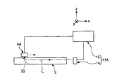
- FIG. 5 is a partial longitudinal sectional view showing a process of manufacturing the optical waveguide module by the method of manufacturing the optical waveguide module of the present invention (second embodiment).
- the optical device mounting position determination method the optical waveguide module manufacturing method, and the second embodiment of the optical waveguide module according to the present invention will be described with reference to this figure.
- the description will focus on differences from the above-described embodiment.
- the description of similar matters is omitted.
- This embodiment is the same as the first embodiment except that the configurations of the optical waveguide module and the optical waveguide module manufacturing apparatus are different from each other.
- an optical element 4 ⁇ / b> A serving as a light receiving element that receives the light L is disposed opposite to the upper side (one surface side) of the optical waveguide 3.
- the optical element 4A for example, an optical element formed of a photodiode can be used.
- a reflecting surface (mirror) 33 is formed in the middle of the optical waveguide 3 in the longitudinal direction at a position corresponding to the optical element 4A, that is, a position directly below the optical element 4A. Yes.
- the reflection surface 33 performs optical path conversion that directs the optical path of the light L passing through the core portion 31 of the optical waveguide 3 upward (in the direction of the optical element 4A).
- the inclination angle ⁇ of the reflecting surface 33 is not particularly limited, but is preferably 20 to 70 °, more preferably 27 to 57 °, and still more preferably 32 to 52 °.
- the inclination angle ⁇ is most preferably 42 ° ⁇ 3.
- the optical waveguide module manufacturing apparatus 11A includes a light emitting element (light emitting apparatus) 14 disposed on the right side of the optical waveguide 3 in FIG.
- the light emitting element 14 includes, for example, a light emitting diode, and can emit light L from the light emitting diode to the reflecting surface 33. Then, the light L from the light emitting element 14 passes through the core portion 31 of the optical waveguide 3 and is reflected by the reflecting surface 33. The reflected light L (reflected light) is received by the optical element 4A.
- the control unit 12 can detect the amount of reflected light received by the optical element 4A.
- the second embodiment is different from the first embodiment in that the positional relationship between the light emitting side element and the light receiving side element is interchanged. Therefore, in the second embodiment, when the optical waveguide module 1 is manufactured by mounting the optical waveguide 3 and the optical element 4A by the manufacturing method substantially the same as that described in the first embodiment, the optical element 4A can be reliably mounted on the optical waveguide 3 at an optically optimal position.
- optical element mounting position determining method the optical waveguide module manufacturing method, and the optical waveguide module according to the present invention have been described above with reference to the illustrated embodiments.
- the present invention is not limited to this, and the optical waveguide module is configured.
- Each part to be replaced can be replaced with one having any configuration capable of performing the same function.
- arbitrary components may be added.
- optical element mounting position determination method may be a combination of any two or more configurations (features) of the above embodiments. .
- the optical waveguide module is one in which either the light emitting element or the light receiving element is mounted in the illustrated configuration, but is not limited to this.
- both optical elements are mounted respectively. It may be a thing.
- the optical waveguide module has a reflective surface disposed in the core portion of the optical waveguide in the configuration shown in the drawing, but is not limited thereto, and a reflective surface is disposed on the extension line outside the core portion. It may be.
- three coordinates are stored in advance as z coordinates that can satisfy the optimum positional relationship, but the present invention is not limited to this, and two or four or more coordinates are stored in advance. May be.
- the optical waveguide module manufacturing apparatus fixes each z coordinate that can satisfy the optimum positional relationship and continuously moves the optical element in the x-axis direction in each case.
- the present invention is not limited to this.
- the optical element may be moved in the x-axis direction while continuously moving in the z-axis direction.
- the optical waveguide module manufacturing apparatus may be configured to move the optical element in the y-axis direction and specify a y-coordinate that can satisfy the optimum positional relationship.
- the optical element when an optical waveguide module is manufactured by mounting an optical waveguide and an optical element, the optical element can be reliably mounted at an optically optimal position with respect to the optical waveguide. Thereby, the loss of light can be prevented or suppressed.
- the optical waveguide module includes a substrate on which the optical waveguide and the optical element are mounted, whether the substrate is a single layer or a laminated body,
- the optically optimal position of the optical element relative to the optical waveguide can be grasped regardless of the configuration of the optical waveguide, and the optical element can be reliably mounted at the position.
- an optical waveguide module can be obtained in which the optical element can be reliably mounted at an optically optimal position with respect to the optical waveguide.
Landscapes
- Physics & Mathematics (AREA)
- General Physics & Mathematics (AREA)
- Optics & Photonics (AREA)
- Optical Couplings Of Light Guides (AREA)
- Optical Integrated Circuits (AREA)
- Led Device Packages (AREA)
Abstract
長尺な板状または帯状をなし、その長手方向の途中に反射面(33)を有する光導波路(3)と、光導波路(3)の一方の面側に配置され、反射面(33)に向けて光を発光する光素子(4)とを備える光導波路モジュールを製造する方法は、光導波路(3)と光素子(4)とを相対的に移動させ、かつ、光素子(4)から光(L)を発光させつつ、光(L)が反射面(33)で反射した反射光の光量を検出し、その検出結果に基づいて、光量が最大となるときの光導波路(3)と光素子(4)との相対的な位置関係を最適位置関係と特定し、最適位置関係を維持した状態で光導波路(3)と光素子(4)とを固定することを特徴とする。
Description
本発明は、光素子実装位置決定方法、光導波路モジュールの製造方法および光導波路モジュールに関する。
本願は、2010年10月1日に、日本に出願された特願2010-224412号に基づき優先権を主張し、その内容をここに援用する。
本願は、2010年10月1日に、日本に出願された特願2010-224412号に基づき優先権を主張し、その内容をここに援用する。
近年注目されている光通信の分野における光部品として、光分岐結合器(光カプラ)、光合分波器等が挙げられ、これらに用いる光導波路モジュール(光導波路型素子)が有望視されている。この光導波路モジュールとしては、従来の石英系光導波路の他、製造(パターニング)が容易で汎用性に富むポリマー系光導波路があり、近年では後者の開発が盛んに行われている。
このような光導波路モジュールは、コア部およびクラッド部で構成される光導波路と、光導波路の両端側にそれぞれ取り付けられる発光素子および受光素子とを備えたものが開示されている(例えば、特許文献1参照)。この特許文献1に記載の光導波路モジュールでは、光導波路の両端部にそれぞれ光を反射する反射面が形成されている。そして、発光素子からの光は、一方の反射面で反射してコア部を通過し、さらに他方の反射面で反射して受光素子で受光される。
しかしながら、特許文献1に記載の光導波路モジュールでは、光導波路に対し発光素子や受光素子を取り付ける際、各光素子の反射面に対する取り付け精度によっては、例えば、発光素子からの光が前記一方の反射面で十分に反射することができなかったり、コア部を通過した光が前記他方の反射面で十分に反射することができなかったりする場合があった。この場合、反射面で光が反射していない分だけ、その光が外部へ漏れることとなり、結果、光の損失が生じるという問題があった。
本発明の目的は、光導波路と光素子とを実装して光導波路モジュールを製造する際に、光素子を光導波路に対して光学的に最適な位置に確実に実装することができる光素子実装位置決定方法、光導波路モジュールの製造方法、および、かかる製法により製造された光導波路モジュールを提供することにある。
このような目的は、下記(1)~(16)の本発明により達成される。
(1) コア部と、該コア部の長手方向の途中に該長手方向に対し傾斜した反射面を有する板状または帯状をなす光導波路と、該光導波路の一方の面側に配置され、前記反射面に向けて光を発光する光素子とを備える光導波路モジュールにおける光素子実装位置決定方法であって、
前記光導波路と前記光素子とを相対的に移動させ、かつ、前記光素子から光を発光させつつ、該光が前記反射面で反射した反射光の光量を検出し、その検出結果に基づいて、前記光量が最大となるときの前記光導波路と前記光素子との相対的な位置関係を最適位置関係と特定することを特徴とする光素子実装位置決定方法。
(1) コア部と、該コア部の長手方向の途中に該長手方向に対し傾斜した反射面を有する板状または帯状をなす光導波路と、該光導波路の一方の面側に配置され、前記反射面に向けて光を発光する光素子とを備える光導波路モジュールにおける光素子実装位置決定方法であって、
前記光導波路と前記光素子とを相対的に移動させ、かつ、前記光素子から光を発光させつつ、該光が前記反射面で反射した反射光の光量を検出し、その検出結果に基づいて、前記光量が最大となるときの前記光導波路と前記光素子との相対的な位置関係を最適位置関係と特定することを特徴とする光素子実装位置決定方法。
(2) コア部と、該コア部の長手方向の途中に該長手方向に対し傾斜した反射面を有する板状または帯状をなす光導波路と、該光導波路の一方の面側に配置され、前記反射面で反射した反射光を受光する光素子とを備える光導波路モジュールにおける光素子実装位置決定方法であって、
前記光導波路と前記光素子とを相対的に移動させ、かつ、前記光導波路の一端側から光を発光しつつ、該光が前記反射面で反射して前記光素子で受光された反射光の光量を検出し、その検出結果に基づいて、前記光量が最大となるときの前記光導波路と前記光素子との相対的な位置関係を最適位置関係と特定することを特徴とする光素子実装位置決定方法。
前記光導波路と前記光素子とを相対的に移動させ、かつ、前記光導波路の一端側から光を発光しつつ、該光が前記反射面で反射して前記光素子で受光された反射光の光量を検出し、その検出結果に基づいて、前記光量が最大となるときの前記光導波路と前記光素子との相対的な位置関係を最適位置関係と特定することを特徴とする光素子実装位置決定方法。
(3) コア部と、該コア部の長手方向の途中に該長手方向に対し傾斜した反射面を有する板状または帯状をなす光導波路と、該光導波路の一方の面側に配置され、前記反射面に向けて光を発光する光素子とを備える光導波路モジュールを製造する方法であって、
前記光導波路と前記光素子とを相対的に移動させ、かつ、前記光素子から光を発光させつつ、該光が前記反射面で反射した反射光の光量を検出し、その検出結果に基づいて、前記光量が最大となるときの前記光導波路と前記光素子との相対的な位置関係を最適位置関係と特定し、該最適位置関係を維持した状態で前記光導波路と前記光素子とを固定することを特徴とする光導波路モジュールの製造方法。
前記光導波路と前記光素子とを相対的に移動させ、かつ、前記光素子から光を発光させつつ、該光が前記反射面で反射した反射光の光量を検出し、その検出結果に基づいて、前記光量が最大となるときの前記光導波路と前記光素子との相対的な位置関係を最適位置関係と特定し、該最適位置関係を維持した状態で前記光導波路と前記光素子とを固定することを特徴とする光導波路モジュールの製造方法。
(4) 前記光導波路の一端側に光を受光する受光装置を設置して、前記反射光の受光を行なう上記(3)に記載の光導波路モジュールの製造方法。
(5) コア部と、該コア部の長手方向の途中に該長手方向に対し傾斜した反射面を有する板状または帯状をなす光導波路と、該光導波路の一方の面側に配置され、前記反射面で反射した反射光を受光する光素子とを備える光導波路モジュールを製造する方法であって、
前記光導波路と前記光素子とを相対的に移動させ、かつ、前記光導波路の一端側から光を発光しつつ、該光が前記反射面で反射して前記光素子で受光された反射光の光量を検出し、その検出結果に基づいて、前記光量が最大となるときの前記光導波路と前記光素子との相対的な位置関係を最適位置関係と特定し、該最適位置関係を維持した状態で前記光導波路と前記光素子とを固定することを特徴とする光導波路モジュールの製造方法。
前記光導波路と前記光素子とを相対的に移動させ、かつ、前記光導波路の一端側から光を発光しつつ、該光が前記反射面で反射して前記光素子で受光された反射光の光量を検出し、その検出結果に基づいて、前記光量が最大となるときの前記光導波路と前記光素子との相対的な位置関係を最適位置関係と特定し、該最適位置関係を維持した状態で前記光導波路と前記光素子とを固定することを特徴とする光導波路モジュールの製造方法。
(6) 前記光導波路の一端側に光を発光する発光装置を設置して、前記反射面への光の発光を行なう上記(5)に記載の光導波路モジュールの製造方法。
(7) 平面視で前記反射面と前記光素子とが重なる範囲内で、前記光導波路と前記光素子との相対的な移動を行なう上記(3)ないし(6)のいずれかに記載の光導波路モジュールの製造方法。
(8) 前記コア部の長手方向をx軸方向、該x軸方向に直交する前記コア部の幅方向をy軸方向、前記x軸方向および前記y軸方向に直交する前記コア部の厚さ方向をz軸方向と想定したとき、前記光導波路と前記光素子とを相対的に移動させる際の前記光素子の前記光導波路に対する移動方向は、前記x軸方向、前記y軸方向および前記z軸方向のうちの少なくとも前記x軸方向および前記z軸方向である上記(3)ないし(7)のいずれかに記載の光導波路モジュールの製造方法。
(9) 前記光導波路の位置を固定し、前記光素子の前記z軸方向の位置を第1のz座標で固定し、その固定状態で前記光素子を前記光導波路に対して前記x軸方向に沿って移動し、その際の前記光素子の各x座標における前記光量をそれぞれ検出し、該各光量の中で最大の第1の光量を記憶する第1の工程と、
前記光導波路の位置を固定し、前記光素子の前記z軸方向の位置を第1のz座標と異なる第2のz座標で固定し、その固定状態で前記光素子を前記光導波路に対して前記x軸方向に沿って移動し、その際の前記光素子の各x座標における前記光量をそれぞれ検出し、該各光量の中で最大の第2の光量を記憶する第2の工程とを有し、
前記第1の光量と前記第2の光量とを比較して一方が他方よりも大となった場合、前記一方の光量を得るときの前記光素子のx座標およびz座標を前記最適位置関係を満足するものとする上記(8)に記載の光導波路モジュールの製造方法。
前記光導波路の位置を固定し、前記光素子の前記z軸方向の位置を第1のz座標と異なる第2のz座標で固定し、その固定状態で前記光素子を前記光導波路に対して前記x軸方向に沿って移動し、その際の前記光素子の各x座標における前記光量をそれぞれ検出し、該各光量の中で最大の第2の光量を記憶する第2の工程とを有し、
前記第1の光量と前記第2の光量とを比較して一方が他方よりも大となった場合、前記一方の光量を得るときの前記光素子のx座標およびz座標を前記最適位置関係を満足するものとする上記(8)に記載の光導波路モジュールの製造方法。
(10) 前記第2の工程を複数回繰り返し、その際、前記各第2のz座標がそれぞれ異なる上記(9)に記載の光導波路モジュールの製造方法。
(11) 前記光導波路モジュールは、前記光導波路および前記光素子が実装される基板を備えるものであり、
前記最適位置関係を維持した状態で前記光導波路と前記光素子との間に前記基板を介挿して、該基板に対し前記光導波路および前記光素子をそれぞれ固定する上記(3)ないし(10)のいずれかに記載の光導波路モジュールの製造方法。
前記最適位置関係を維持した状態で前記光導波路と前記光素子との間に前記基板を介挿して、該基板に対し前記光導波路および前記光素子をそれぞれ固定する上記(3)ないし(10)のいずれかに記載の光導波路モジュールの製造方法。
(12) 前記基板は、厚さが異なるものが複数枚用意されており、該複数枚の基板の中から前記最適位置関係を規制し得る1枚の基板を選択する上記(11)に記載の光導波路モジュールの製造方法。
(13) 接着剤層を介して前記光導波路を前記基板に固定し、半田を介して前記光素子を前記基板に固定する上記(11)または(12)に記載の光導波路モジュールの製造方法。
(14) 前記光導波路は、コア部とクラッド部とを有しており、
前記反射面は、前記コア部と前記クラッド部とをまたいで形成されている上記(3)ないし(13)のいずれかに記載の光導波路モジュールの製造方法。
前記反射面は、前記コア部と前記クラッド部とをまたいで形成されている上記(3)ないし(13)のいずれかに記載の光導波路モジュールの製造方法。
(15) 前記反射面の傾斜角度は、20~70°である上記(3)ないし(14)のいずれかに記載の光導波路モジュールの製造方法。
(16) 上記(3)ないし(15)のいずれかに記載の光導波路モジュールの製造方法により製造されたことを特徴とする光導波路モジュール。
(16) 上記(3)ないし(15)のいずれかに記載の光導波路モジュールの製造方法により製造されたことを特徴とする光導波路モジュール。
本発明によれば、光導波路と光素子とを実装して光導波路モジュールを製造する際に、光素子を光導波路に対して光学的に最適な位置に確実に実装することができる。これにより、光の損失を防止または抑制することができる。
また、光導波路モジュールが光導波路および光素子が実装される基板を備える場合には、基板が単層のものであっても、積層体で構成されたものであっても、その基板の構成や、その他光導波路の構成によらず、光導波路に対する光素子の光学的に最適な位置を把握することができ、当該位置に光素子を確実に実装することができる。
また、このように光素子を光導波路に対して光学的に最適な位置に確実に実装することができた光導波路モジュールを得る。
以下、本発明の光素子実装位置決定方法、光導波路モジュールの製造方法および光導波路モジュールを添付図面に示す好適な実施形態に基づいて詳細に説明する。
<第1実施形態>
図1~図3は、それぞれ、本発明の光導波路モジュールの製造方法(第1実施形態)により光導波路モジュールを製造する過程を模式的に順に示す部分縦断面図、図4は、x軸方向に移動する光素子から発光される光が受光装置で受光されたときの光量の変化を示すグラフである。なお、以下では、説明の都合上、図1~図3中(図5についても同様)の上側を「上」または「上方」、下側を「下」または「下方」と言う。また、図1~図3中(図5についても同様)の左右方向(光導波路の長手方向)をx軸方向、x軸方向に直交する紙面奥行き方向(光導波路の幅方向)をy軸方向、x軸方向およびy軸方向に直交する上下方向(光導波路の厚さ方向)をz軸方向とする。
図1~図3は、それぞれ、本発明の光導波路モジュールの製造方法(第1実施形態)により光導波路モジュールを製造する過程を模式的に順に示す部分縦断面図、図4は、x軸方向に移動する光素子から発光される光が受光装置で受光されたときの光量の変化を示すグラフである。なお、以下では、説明の都合上、図1~図3中(図5についても同様)の上側を「上」または「上方」、下側を「下」または「下方」と言う。また、図1~図3中(図5についても同様)の左右方向(光導波路の長手方向)をx軸方向、x軸方向に直交する紙面奥行き方向(光導波路の幅方向)をy軸方向、x軸方向およびy軸方向に直交する上下方向(光導波路の厚さ方向)をz軸方向とする。
まず、光導波路モジュール1について説明する。
図3に示す光導波路モジュール1は、基板2と、基板2の下側に実装された光導波路3と、基板2の上側に実装された光素子4とを備えている。
図3に示す光導波路モジュール1は、基板2と、基板2の下側に実装された光導波路3と、基板2の上側に実装された光素子4とを備えている。
基板2は、長尺な板状をなす基板本体21と、基板本体21の上面に設けられた電気回路22とで構成されている。
ここで、基板本体21の長手方向の長さは、限定されないが、例えば、1mm~10m程度、好ましくは3mm~5m程度である。また、基板本体21の幅は、限定されないが、例えば、60μm~2m程度、好ましくは100μm~1m程度である。
ここで、基板本体21の長手方向の長さは、限定されないが、例えば、1mm~10m程度、好ましくは3mm~5m程度である。また、基板本体21の幅は、限定されないが、例えば、60μm~2m程度、好ましくは100μm~1m程度である。
基板本体21は、比較的剛性の高い剛性基板であってもよいし、可撓性を有する可撓性基板であってもよいが、剛性基板であるのが好ましい。基板本体21が剛性基板である場合には、耐屈曲性が高くなり、屈曲に伴う光素子4の基板本体21からの離脱等を防止することができる。
基板本体21のヤング率(引張弾性率)は、一般的な室温環境下(20~25℃前後)で5~50GPa程度であるのが好ましく、12~30GPa程度であるのがより好ましい。ヤング率の範囲がこの程度であれば、基板本体21は、上述したような効果をより確実に発揮することができる。
このような基板本体21の構成材料としては、例えば、紙、ガラス布、樹脂フィルム等を基材とし、この基材に、フェノール系樹脂、ポリエステル系樹脂、エポキシ系樹脂、シアネート樹脂、ポリイミド系樹脂、フッ素系樹脂等の樹脂材料を含浸させたものが挙げられる。具体的には、ガラス布・エポキシ銅張積層板、ガラス不織布・エポキシ銅張積層板等のコンポジット銅張積層板に使用される絶縁性基板の他、ポリエーテルイミド樹脂基板、ポリエーテルケトン樹脂基板、ポリサルフォン系樹脂基板等の耐熱・熱可塑性の有機系リジッド基板や、アルミナ基板、窒化アルミニウム基板、炭化ケイ素基板等のセラミックス系リジッド基板等が挙げられる。
また、基板本体21が上述したような材料で構成される場合、その厚さt1は、例えば、5μm~5mmであるのが好ましく、5μm~3mmであるのがより好ましい。
基板本体21の上面には、電気回路22が設けられている。電気回路22は、基板本体21の上面に積層され、導電性を有する金属材料(例えば銅)で構成された導体層を例えばエッチングにより所定のパターンをなすように形成されたものである。
基板2の下側には、光導波路3が配置されている。この光導波路3は、長尺な帯状または板状をなすものであり、長尺な線状のコア部31と、コア部31の周囲を囲むように設けられた筒状のクラッド部32とで構成されている。
ここで、光導波路3の長手方向の長さは、限定されないが、例えば、1mm~10m程度、より好ましくは3mm~5m程度である。
コア部31に入射した光Lは、コア部31とクラッド部32との界面で反射を繰り返しながら、コア部31内をその長手方向に沿って進む。
ここで、光導波路3の長手方向の長さは、限定されないが、例えば、1mm~10m程度、より好ましくは3mm~5m程度である。
コア部31に入射した光Lは、コア部31とクラッド部32との界面で反射を繰り返しながら、コア部31内をその長手方向に沿って進む。
光導波路3の横断面形状は、好ましくは正方形または矩形(長方形)のような四角形とされる。なお、光導波路3の厚さt2は、例えば、15~200μm程度であるのが好ましく、30~100μm程度であるのがより好ましい。
また、コア部31の幅および厚さは、特に限定されないが、1~200μm程度であるのが好ましく、5~100μm程度であるのがより好ましく、10~60μm程度であるのがさらに好ましい。一方、クラッド部32の厚さは、3~50μm程度であるのが好ましく、5~30μm程度であるのがより好ましい。
また、コア部31とクラッド部32とは、互いに光の屈折率が異なり、その屈折率の差は、0.5%以上であるのが好ましく、0.8%以上であるのがより好ましい。一方、上限値は、特に設定されなくてもよいが、好ましくは5.5%程度とされる。屈折率の差が前記下限値未満であると光を伝達する効果が低下する場合があり、前記上限値を超えても、光の伝送効率のそれ以上の増大は期待できない。
なお、前記屈折率差とは、コア部31の屈折率をA、クラッド部32の屈折率をBとしたとき、次式で表される。
屈折率差(%)=|A/B-1|×100
屈折率差(%)=|A/B-1|×100
コア部31、クラッド部32の各構成材料は、それぞれ上記の屈折率差が生じる材料であれば特に限定されないが、具体的には、アクリル系樹脂、メタクリル系樹脂、ポリカーボネート、ポリスチレン、エポキシ樹脂、ポリアミド、ポリイミド、ポリベンゾオキサゾール、ポリシラン、ポリシラザン、また、ベンゾシクロブテン系樹脂やノルボルネン系樹脂等の環状オレフィン系樹脂のような各種樹脂材料の他、石英ガラス、ホウケイ酸ガラスのようなガラス材料等を用いることができる。
図3に示すように、光導波路3の長手方向の途中には、光素子4に対応する位置、すなわち、光素子4の直下となる位置に、反射面(ミラー)33が形成されている。この反射面33は、光導波路3の上方(光素子4)から入射された光がコア部31に向けて反射されるよう光路を直角に変換する光路変換を担う(図1参照)。
反射面33は、コア部31とクラッド部32とをまたいで、光導波路3の長手方向に対し傾斜して形成された部分である。これにより、反射面33の形成面積をできる限り広く確保することができ、よって、光Lを反射面33に確実に当てて、反射させることができる。
なお、反射面33の傾斜角度θは、特に限定されないが、例えば、20~70°であるのが好ましく、30~60°であるのがより好ましく、35~55°であるのがより更に好ましい。特に、傾斜角度θを45°±3とするのが最も好ましい。
また、反射面33は、光導波路3に例えばレーザ加工、研削加工等を施すことにより形成される。
また、反射面33に必要に応じて反射膜を成膜してもよい。この反射膜としては、Au、Ag、Al等の金属膜が好ましく用いられる。
以上のような構成の光導波路3は、接着剤層5を介して基板2に固定される。接着剤層5を構成する接着剤としては、特に限定されず、例えば、シリコーン系、エポキシ系、アクリル系、シアノアクリレート系、ポリウレタン系等の、紫外線硬化型、可視光硬化型、または電子線硬化型の接着剤を好適に用いることができる。接着剤層5が粘着剤で構成されている場合、その粘着剤としては、特に限定されず、例えば、ゴム系、アクリル系、シリコーン系、ウレタン系等の粘着剤を好適に用いることができる。これにより、光導波路3が基板2に対し確実に固定され、光導波路モジュール1の使用中に光導波路3が不本意に離脱するのが防止される。
図3に示すように、基板2の上側には、光導波路3の反射面33に臨むように光素子4が配置されている。この光素子4は、小片状をなすものであり、下面側に発光部41と端子42、43とが設けられている。発光部41は、光素子4の下面の中央部に配置され、端子42と端子43とは、発光部41を介して互いに反対側に配置されている。
また、光素子4は、端子42、43がそれぞれ半田23、24を介して基板2の電気回路22と電気的に接続され、固定もされている。
そして、光素子4は、電気回路22を介して電力が供給されて、端子42、43間に通電がなされると、発光部41が発光する。この発光部41から発光された光Lは、反射面33に向うこととなり、当該反射面33で反射して光導波路3のコア部31を通過することができる。
このような発光素子である光素子4としては、例えば、発光ダイオード(LED)を有する素子を用いることができる。
なお、基板2には、発光部41からの光Lが通過する光路となる部分に、その厚さ方向に貫通する貫通孔(スルーホール)が形成されていてもよい。
次に、以上のような構成の光導波路モジュール1を製造する製造方法(光素子実装位置決定方法)について説明する。この製造方法は、図1に示す光導波路モジュール製造装置11を用いて行なわれる。
なお、この製造方法で製造された光導波路モジュール1を、例えば光素子4の光Lを受光する受光部が内蔵された電子機器に設置して用いる場合、当該光導波路モジュール1は、前記受光部での光量(受光量)ができる限り大となるように、反射面33で反射した光Lを前記受光部に向けて投光することができるものであるが好ましい。このような光導波路モジュール1は、光量が最大となるように、光導波路3と光素子4との相対的な位置関係、すなわち、位置が固定された光導波路3に対する光素子4のx座標、y座標およびz座標が好適に規制されたものである。以下、このときの位置関係を「最適位置関係」と言う。
そして、光導波路モジュール製造装置11は、最適位置関係を特定する装置である。光導波路モジュール製造装置11は、制御部12と受光素子(受光装置)13とを備えている。
受光素子13は、例えばフォトダイオードで構成され、光導波路3の一端側(図1中の右側)、すなわち、光Lの進行方向前方に設置されている。そして、受光素子13は、反射面33で反射した光L(反射光)を受光することができる。
制御部12は、例えば、パーソナルコンピュータやマイクロコンピュータの中央演算装置(CPU)とメモリのような記憶媒体とで構成されたものであり、必要に応じ、キーボードのような外部入力手段、ハードディスクのような記録媒体への記録手段、他のコンピュータ等との通信手段等を備えている。この制御部12は、受光素子13と、光導波路モジュール1に搭載される発光素子としての光素子4と電気的に接続されている。そして、制御部12は、受光素子13および光素子4の作動を制御したり、受光素子13で受光した光Lの光量の検出および記憶を行なう等をすることができる。
また、光導波路モジュール製造装置11は、光素子4をx軸方向、y軸方向およびz軸方向にそれぞれ移動することができる移動機構(図示せず)を備えている。この移動機構は、例えば、制御部12で作動が制御されるモータと、モータに連結されたボールネジと、ボールネジに連結され、移動する光素子4を案内するリニアガイドとを備えている。
最適位置関係を満足する、光導波路3に対する光素子4のx座標、y座標およびz座標のうち、y座標の位置精度の高低は、x座標およびz座標の各位置精度に比べて、前記電子機器の受光部で受光される光量の大小への影響、すなわち、光の損失に対する影響が小さいことが一般的に知られている。
そこで、本実施形態では、光導波路モジュール製造装置11を、最適位置関係を満足する光素子4のx座標およびz座標を特定するのに用いる。以下、これについて説明する。
図1に示すように、光導波路モジュール製造装置11では、最適位置関係を満足し得ると予想されるz座標として「z1」、「z2」、「z3」が予め制御部12に記憶されている。z1、z2、z3の大小関係は、z1<z2<z3である。光素子4は、z=z1のときに光導波路3に最も接近しており、z=z3のときに光導波路3から最も離間しており、z=z2のときにその中間に位置している。
そして、光導波路モジュール製造装置11は、後述するように、光素子4をz1~z3の各z座標の位置で固定して、その固定状態で光素子4をx軸方向に沿って連続的に移動させることができる。なお、光素子4の移動範囲は、平面視で反射面33と光素子4の発光部41とが重なる範囲とするのが好ましい。これにより、最適位置関係を満足し得ると予想されるx座標の全てを確実に検出することができる。
まず、図1中の「I:z=z1」の図(a)~(c)に示すように、光導波路3の位置を固定するとともに、光素子4のz軸方向の位置をz=z1(第1のz座標)で固定し、その固定状態で光素子4を光導波路3に対してx軸方向(図1中の矢印方向)に沿って移動させる。また、この移動に伴って、光素子4の発光部41から光Lを発光させる。
光Lは、反射面33でその傾斜方向に沿って、すなわち、反射面33上の異なる位置で反射しつつ、受光素子13で受光される。これにより、制御部12では、光素子4の各x座標における光量がそれぞれ検出され、図4に示すような光量分布グラフ(「z=z1」のときのもの)を得る。そして、制御部12は、このグラフから各光量の中で最大光量p1(第1の光量)を判断して、それを記憶する(第1の工程)。なお、最大光量p1の判断は、グラフ上で光量が増加から減少に転じる点を「最大光量p1」と判断する。また、最大光量p1となるときのx座標は、「x1」である。このx=x1も制御部12に記憶される。
次に、図1中の「II:z=z2」の図(a)~(c)に示すように、光導波路3を前記と同じ位置で固定するとともに、光素子4のz軸方向の位置をz=z2(第2のz座標)で固定し、その固定状態で光素子4を光導波路3に対してx軸方向(図1中の矢印方向)に沿って移動させる。また、この移動に伴って、光素子4の発光部41から光Lを発光させる。
このときも光Lは、反射面33でその傾斜方向に沿って反射しつつ、受光素子13で受光される。これにより、制御部12では、光素子4の各x座標における光量がそれぞれ検出され、図4に示すような光量分布グラフ(「z=z2」のときのもの)を得る。そして、制御部12は、このグラフから各光量の中で最大光量p2(第2の光量)を判断して、それを記憶する(第2の工程)。なお、最大光量p2の判断は、グラフ上で光量が増加から減少に転じる点を「最大光量p2」と判断する。また、最大光量p2となるときのx座標は、「x2」である。このx=x2も制御部12に記憶される。
次に、図1中の「III:z=z3」の図(a)~(c)に示すように、光導波路3を前記と同じ位置で固定するとともに、光素子4のz軸方向の位置をz=z3(第2のz座標)で固定し、その固定状態で光素子4を光導波路3に対してx軸方向(図1中の矢印方向)に沿って移動させる。また、この移動に伴って、光素子4の発光部41から光Lを発光させる。
このときも光Lは、反射面33でその傾斜方向に沿って反射しつつ、受光素子13で受光される。これにより、制御部12では、光素子4の各x座標における光量がそれぞれ検出され、図4に示すような光量分布グラフ(「z=z3」のときのもの)を得る。そして、制御部12は、このグラフから各光量の中で最大光量p3(第2の光量)を判断して、それを記憶する(第2の工程)。なお、最大光量p3の判断は、グラフ上で光量が増加から減少に転じる点を「最大光量p3」と判断する。また、最大光量p3となるときのx座標は、「x3」である。このx=x3も制御部12に記憶される。
次に、制御部12では、「I:z=z1」、「II:z=z2」および「III:z=z3」における検出結果である最大光量p1~p3の大小関係を比較して、本実施形態ではp3<p1<p2となっており、これらの中から最大のもの、すなわち、最大光量p2を検出する。そして、最大光量p2となるときの光素子4のx座標「x2」、z座標「z2」を最適位置関係を満足する座標と特定する。
次に、図2に示すように、最適位置関係を維持した状態、すなわち、光導波路3に対し光素子4を座標(x,z)=(x2,z2)に位置決めした状態で、光導波路3と光素子4とをそれぞれ基板2に対し固定する。
ところで、基板2として、3枚の基板2a、2b、2cが用意されている。基板2a~2cは、それぞれ、基板本体21の厚さt1が異なるものである。基板2aは、最適位置関係を満足する座標が(x,z)=(x1,z1)となったときに用いられるものである。基板2bは、最適位置関係を満足する座標が(x,z)=(x2,z2)となったときに用いられるものである。基板2cは、最適位置関係を満足する座標が(x,z)=(x3,z3)となったときに用いられるものである。
そして、基板2a~2cの中から1枚の基板2を選択するのであるが、前述したように最適位置関係を満足する座標が(x,z)=(x2,z2)であるので、基板2bを選択することができる。
なお、基板2a~2cには、それぞれ、半田23および24と、接着剤層5とが予め設けられている。
次に、図3に示すように、前記最適位置関係を維持した状態の光導波路3と光素子4との間に基板2bを介挿する。その後、リフロー処理を行ない、半田23および24を介して基板2bと光素子4とを固定する。また、接着剤層5をそれに適した硬化方法により硬化させて、接着剤層5を介して基板2bと光導波路3とを固定する。
このように製造された光導波路モジュール1は、光導波路3と光素子4とが最適位置関係で確実に規制されたものとなる。これにより、光導波路モジュール1を前記電子機器に設置して用いれば、前記受光部での光量ができる限り大となるように、光Lを前記受光部に向けて確実に投光することができる。
従って、光導波路3と光素子4とを基板2に実装して光導波路モジュール1を製造する際に、本製造方法を用いることにより、光素子4を光導波路3に対して光学的に最適な位置、すなわち、前記受光部での光量ができる限り大となるような位置に確実に実装することができる。
<第2実施形態>
図5は、本発明の光導波路モジュールの製造方法(第2実施形態)により光導波路モジュールを製造する過程を示す部分縦断面図である。
図5は、本発明の光導波路モジュールの製造方法(第2実施形態)により光導波路モジュールを製造する過程を示す部分縦断面図である。
以下、この図を参照して本発明の光素子実装位置決定方法、光導波路モジュールの製造方法および光導波路モジュールの第2実施形態について説明するが、前述した実施形態との相違点を中心に説明し、同様の事項はその説明を省略する。
本実施形態は、光導波路モジュールおよび光導波路モジュール製造装置の構成がそれぞれ異なること以外は前記第1実施形態と同様である。
図5に示すように、光導波路3の上側(一方の面側)に対向して配置されるものは、光Lを受光する受光素子としての光素子4Aである。光素子4Aとしては、例えば、フォトダイオードで構成されたものを用いることができる。
前記第1実施形態と同様に、光導波路3の長手方向の途中には、光素子4Aに対応する位置、すなわち、光素子4Aの直下となる位置に、反射面(ミラー)33が形成されている。この反射面33は、光導波路3のコア部31を通過する光Lの光路を上方(光素子4A方向)に向ける光路変換を担う。
反射面33の傾斜角度θは、特に限定されないが、例えば、20~70°であるのが好ましく、27~57°であるのがより好ましく、32~52°であるのがより更に好ましい。特に、傾斜角度θを42°±3とするのが最も好ましい。
前記第1実施形態と同様に、光導波路3の長手方向の途中には、光素子4Aに対応する位置、すなわち、光素子4Aの直下となる位置に、反射面(ミラー)33が形成されている。この反射面33は、光導波路3のコア部31を通過する光Lの光路を上方(光素子4A方向)に向ける光路変換を担う。
反射面33の傾斜角度θは、特に限定されないが、例えば、20~70°であるのが好ましく、27~57°であるのがより好ましく、32~52°であるのがより更に好ましい。特に、傾斜角度θを42°±3とするのが最も好ましい。
光導波路モジュール製造装置11Aは、光導波路3の図5中の右側に配置された発光素子(発光装置)14を備えている。発光素子14は、例えば発光ダイオードを有し、当該発光ダイオードから反射面33への光Lを発光することができる。そして、発光素子14からの光Lは、光導波路3のコア部31を通過して、反射面33で反射する。この反射した光L(反射光)は、光素子4Aで受光される。光導波路モジュール製造装置11Aでは、制御部12が光素子4Aで受光された反射光の光量を検出することができる。
このように、第2実施形態は、発光側の素子と受光側の素子との位置関係が入れ替わった点が第1実施形態と異なっている。このため、第2実施形態でも、前記第1実施形態で述べたのとほぼ同様の製造方法により、光導波路3と光素子4Aとを実装して光導波路モジュール1を製造する際に、光素子4Aを光導波路3に対して光学的に最適な位置に確実に実装することができる。
以上、本発明の光素子実装位置決定方法、光導波路モジュールの製造方法および光導波路モジュールを図示の実施形態について説明したが、本発明は、これに限定されるものではなく、光導波路モジュールを構成する各部は、同様の機能を発揮し得る任意の構成のものと置換することができる。また、任意の構成物が付加されていてもよい。
また、本発明の光素子実装位置決定方法、光導波路モジュールの製造方法および光導波路モジュールは、前記各実施形態のうちの、任意の2以上の構成(特徴)を組み合わせたものであってもよい。
例えば、光導波路モジュールは、図示の構成では発光素子および受光素子のいずれか一方の光素子が搭載されたものであるが、これに限定されず、例えば、双方の光素子がそれぞれ搭載されていたものであってもよい。
また、光導波路モジュールは、図示の構成では光導波路のコア部内に反射面が配置されたものであるが、これに限定されず、コア部の外部でその延長線上に反射面が配置されたものであってもよい。
また、光導波路モジュール製造装置には、最適位置関係を満足し得るz座標として3つの座標が予め記憶されていたが、これに限定されず、2つまたは4つ以上の座標が予め記憶されていてもよい。
また、光導波路モジュール製造装置は、最適位置関係を満足し得る各z座標を固定して、それぞれの場合で光素子をx軸方向に連続的に移動させるものであるが、これに限定されず、光素子をz軸方向にも連続的に移動させつつ、x軸方向への移動を行なってもよい。
また、光導波路モジュール製造装置は、光素子をy軸方向へも移動させ、最適位置関係を満足し得るy座標を特定するよう構成されていてもよい。
本発明によれば、光導波路と光素子とを実装して光導波路モジュールを製造する際に、光素子を光導波路に対して光学的に最適な位置に確実に実装することができる。これにより、光の損失を防止または抑制することができる。
また、光導波路モジュールが光導波路および光素子が実装される基板を備える場合には、基板が単層のものであっても、積層体で構成されたものであっても、その基板の構成や、その他光導波路の構成によらず、光導波路に対する光素子の光学的に最適な位置を把握することができ、当該位置に光素子を確実に実装することができる。
また、このように光素子を光導波路に対して光学的に最適な位置に確実に実装することができた光導波路モジュールを得ることができる。
1 光導波路モジュール
2、2a、2b、2c 基板
21 基板本体
22 電気回路
23、24 半田
3 光導波路
31 コア部
32 クラッド部
33 反射面(ミラー)
4、4A 光素子
41 発光部
42、43 端子
5 接着剤層
11、11A 光導波路モジュール製造装置
12 制御部
13 受光素子(受光装置)
14 発光素子(発光装置)
L 光
p1、p2、p3 最大光量
t1、t2 厚さ
x1、x2、x3、z1、z2、z3 座標
θ 傾斜角度
2、2a、2b、2c 基板
21 基板本体
22 電気回路
23、24 半田
3 光導波路
31 コア部
32 クラッド部
33 反射面(ミラー)
4、4A 光素子
41 発光部
42、43 端子
5 接着剤層
11、11A 光導波路モジュール製造装置
12 制御部
13 受光素子(受光装置)
14 発光素子(発光装置)
L 光
p1、p2、p3 最大光量
t1、t2 厚さ
x1、x2、x3、z1、z2、z3 座標
θ 傾斜角度
Claims (16)
- コア部と、該コア部の長手方向の途中に該長手方向に対し傾斜した反射面を有する板状または帯状をなす光導波路と、該光導波路の一方の面側に配置され、前記反射面に向けて光を発光する光素子とを備える光導波路モジュールにおける光素子実装位置決定方法であって、
前記光導波路と前記光素子とを相対的に移動させ、かつ、前記光素子から光を発光させつつ、該光が前記反射面で反射した反射光の光量を検出し、その検出結果に基づいて、前記光量が最大となるときの前記光導波路と前記光素子との相対的な位置関係を最適位置関係と特定することを特徴とする光素子実装位置決定方法。 - コア部と、該コア部の長手方向の途中に該長手方向に対し傾斜した反射面を有する板状または帯状をなす光導波路と、該光導波路の一方の面側に配置され、前記反射面で反射した反射光を受光する光素子とを備える光導波路モジュールにおける光素子実装位置決定方法であって、
前記光導波路と前記光素子とを相対的に移動させ、かつ、前記光導波路の一端側から光を発光しつつ、該光が前記反射面で反射して前記光素子で受光された反射光の光量を検出し、その検出結果に基づいて、前記光量が最大となるときの前記光導波路と前記光素子との相対的な位置関係を最適位置関係と特定することを特徴とする光素子実装位置決定方法。 - コア部と、該コア部の長手方向の途中に該長手方向に対し傾斜した反射面を有する板状または帯状をなす光導波路と、該光導波路の一方の面側に配置され、前記反射面に向けて光を発光する光素子とを備える光導波路モジュールを製造する方法であって、
前記光導波路と前記光素子とを相対的に移動させ、かつ、前記光素子から光を発光させつつ、該光が前記反射面で反射した反射光の光量を検出し、その検出結果に基づいて、前記光量が最大となるときの前記光導波路と前記光素子との相対的な位置関係を最適位置関係と特定し、該最適位置関係を維持した状態で前記光導波路と前記光素子とを固定することを特徴とする光導波路モジュールの製造方法。 - 前記光導波路の一端側に光を受光する受光装置を設置して、前記反射光の受光を行なう請求項3に記載の光導波路モジュールの製造方法。
- コア部と、該コア部の長手方向の途中に該長手方向に対し傾斜した反射面を有する板状または帯状をなす光導波路と、該光導波路の一方の面側に配置され、前記反射面で反射した反射光を受光する光素子とを備える光導波路モジュールを製造する方法であって、
前記光導波路と前記光素子とを相対的に移動させ、かつ、前記光導波路の一端側から光を発光しつつ、該光が前記反射面で反射して前記光素子で受光された反射光の光量を検出し、その検出結果に基づいて、前記光量が最大となるときの前記光導波路と前記光素子との相対的な位置関係を最適位置関係と特定し、該最適位置関係を維持した状態で前記光導波路と前記光素子とを固定することを特徴とする光導波路モジュールの製造方法。 - 前記光導波路の一端側に光を発光する発光装置を設置して、前記反射面への光の発光を行なう請求項5に記載の光導波路モジュールの製造方法。
- 平面視で前記反射面と前記光素子とが重なる範囲内で、前記光導波路と前記光素子との相対的な移動を行なう請求項3ないし6のいずれかに記載の光導波路モジュールの製造方法。
- 前記コア部の長手方向をx軸方向、該x軸方向に直交する前記コア部の幅方向をy軸方向、前記x軸方向および前記y軸方向に直交する前記コア部の厚さ方向をz軸方向と想定したとき、前記光導波路と前記光素子とを相対的に移動させる際の前記光素子の前記光導波路に対する移動方向は、前記x軸方向、前記y軸方向および前記z軸方向のうちの少なくとも前記x軸方向および前記z軸方向である請求項3ないし7のいずれかに記載の光導波路モジュールの製造方法。
- 前記光導波路の位置を固定し、前記光素子の前記z軸方向の位置を第1のz座標で固定し、その固定状態で前記光素子を前記光導波路に対して前記x軸方向に沿って移動し、その際の前記光素子の各x座標における前記光量をそれぞれ検出し、該各光量の中で最大の第1の光量を記憶する第1の工程と、
前記光導波路の位置を固定し、前記光素子の前記z軸方向の位置を第1のz座標と異なる第2のz座標で固定し、その固定状態で前記光素子を前記光導波路に対して前記x軸方向に沿って移動し、その際の前記光素子の各x座標における前記光量をそれぞれ検出し、該各光量の中で最大の第2の光量を記憶する第2の工程とを有し、
前記第1の光量と前記第2の光量とを比較して一方が他方よりも大となった場合、前記一方の光量を得るときの前記光素子のx座標およびz座標を前記最適位置関係を満足するものとする請求項8に記載の光導波路モジュールの製造方法。 - 前記第2の工程を複数回繰り返し、その際、前記各第2のz座標がそれぞれ異なる請求項9に記載の光導波路モジュールの製造方法。
- 前記光導波路モジュールは、前記光導波路および前記光素子が実装される基板を備えるものであり、
前記最適位置関係を維持した状態で前記光導波路と前記光素子との間に前記基板を介挿して、該基板に対し前記光導波路および前記光素子をそれぞれ固定する請求項3ないし10のいずれかに記載の光導波路モジュールの製造方法。 - 前記基板は、厚さが異なるものが複数枚用意されており、該複数枚の基板の中から前記最適位置関係を規制し得る1枚の基板を選択する請求項11に記載の光導波路モジュールの製造方法。
- 接着剤層を介して前記光導波路を前記基板に固定し、半田を介して前記光素子を前記基板に固定する請求項11または12に記載の光導波路モジュールの製造方法。
- 前記光導波路は、コア部とクラッド部とを有しており、
前記反射面は、前記コア部と前記クラッド部とをまたいで形成される請求項3ないし13のいずれかに記載の光導波路モジュールの製造方法。 - 前記反射面の傾斜角度は、20~70°である請求項3ないし14のいずれかに記載の光導波路モジュールの製造方法。
- 請求項3ないし15のいずれかに記載の光導波路モジュールの製造方法により製造されたことを特徴とする光導波路モジュール。
Applications Claiming Priority (2)
| Application Number | Priority Date | Filing Date | Title |
|---|---|---|---|
| JP2010224412A JP2013257352A (ja) | 2010-10-01 | 2010-10-01 | 光素子実装位置決定方法、光導波路モジュールの製造方法および光導波路モジュール |
| JP2010-224412 | 2010-10-01 |
Publications (1)
| Publication Number | Publication Date |
|---|---|
| WO2012043671A1 true WO2012043671A1 (ja) | 2012-04-05 |
Family
ID=45893110
Family Applications (1)
| Application Number | Title | Priority Date | Filing Date |
|---|---|---|---|
| PCT/JP2011/072266 Ceased WO2012043671A1 (ja) | 2010-10-01 | 2011-09-28 | 光素子実装位置決定方法、光導波路モジュールの製造方法および光導波路モジュール |
Country Status (3)
| Country | Link |
|---|---|
| JP (1) | JP2013257352A (ja) |
| TW (1) | TW201222039A (ja) |
| WO (1) | WO2012043671A1 (ja) |
Citations (3)
| Publication number | Priority date | Publication date | Assignee | Title |
|---|---|---|---|---|
| JPH03184006A (ja) * | 1989-12-14 | 1991-08-12 | Fujitsu Ltd | 光半導体モジュール構造 |
| JP2000292656A (ja) * | 1999-04-01 | 2000-10-20 | Sony Corp | 光伝送装置および光伝送装置の製造方法 |
| JP2006093238A (ja) * | 2004-09-21 | 2006-04-06 | Fuji Xerox Co Ltd | 半導体集積回路、半導体集積回路配置装置及び方法 |
-
2010
- 2010-10-01 JP JP2010224412A patent/JP2013257352A/ja active Pending
-
2011
- 2011-09-28 WO PCT/JP2011/072266 patent/WO2012043671A1/ja not_active Ceased
- 2011-09-29 TW TW100135245A patent/TW201222039A/zh unknown
Patent Citations (3)
| Publication number | Priority date | Publication date | Assignee | Title |
|---|---|---|---|---|
| JPH03184006A (ja) * | 1989-12-14 | 1991-08-12 | Fujitsu Ltd | 光半導体モジュール構造 |
| JP2000292656A (ja) * | 1999-04-01 | 2000-10-20 | Sony Corp | 光伝送装置および光伝送装置の製造方法 |
| JP2006093238A (ja) * | 2004-09-21 | 2006-04-06 | Fuji Xerox Co Ltd | 半導体集積回路、半導体集積回路配置装置及び方法 |
Also Published As
| Publication number | Publication date |
|---|---|
| JP2013257352A (ja) | 2013-12-26 |
| TW201222039A (en) | 2012-06-01 |
Similar Documents
| Publication | Publication Date | Title |
|---|---|---|
| KR102094552B1 (ko) | 광전기 혼재 기판 | |
| KR102576475B1 (ko) | 광 전기 혼재 기판 | |
| KR101262499B1 (ko) | 광 인쇄회로기판 및 그의 제조 방법 | |
| JP2015129795A (ja) | 光ファイバコネクタ及び光通信モジュール | |
| KR102523319B1 (ko) | 광전기 혼재 기판 및 그 제법 | |
| KR100871252B1 (ko) | 광섬유를 이용한 광/전기 배선을 갖는 연성 인쇄회로기판 | |
| JP2001166165A (ja) | 接着シート付き導波路フィルム及びその実装方法 | |
| JP2010152111A (ja) | 光導波路、光モジュール、光モジュールの製造方法、および光導波路の製造方法 | |
| JP4932606B2 (ja) | 光送受信装置 | |
| JP2010164856A (ja) | 光学モジュール | |
| JP4582145B2 (ja) | 導波路装置 | |
| JP5593390B2 (ja) | 光印刷回路基板及びその製造方法 | |
| JP2007072007A (ja) | 光導波路モジュール | |
| JP6774885B2 (ja) | 光ファイバ実装構造及び光モジュール | |
| JP2013257352A (ja) | 光素子実装位置決定方法、光導波路モジュールの製造方法および光導波路モジュール | |
| JP2008102283A (ja) | 光導波路、光モジュール及び光導波路の製造方法 | |
| JP2012503784A (ja) | 偏光維持大コア中空導波路 | |
| US20090116787A1 (en) | Optical Waveguide Device and Method for Fabricating Optical Waveguide Device | |
| KR20190088474A (ko) | 광 전기 혼재 기판 | |
| JP6168598B2 (ja) | 光電気混載モジュール | |
| JP4609311B2 (ja) | 光送受信器 | |
| KR101049709B1 (ko) | 발광 소자가 형성된 광 도파로, 및 그것을 구비한 광학식 터치 패널 | |
| JP2010122308A (ja) | 光伝送装置及び光導波路 | |
| JP6551077B2 (ja) | 光モジュール | |
| KR100970395B1 (ko) | 광도파로 디바이스 및 광도파로 디바이스 제조 방법 |
Legal Events
| Date | Code | Title | Description |
|---|---|---|---|
| 121 | Ep: the epo has been informed by wipo that ep was designated in this application |
Ref document number: 11829224 Country of ref document: EP Kind code of ref document: A1 |
|
| NENP | Non-entry into the national phase |
Ref country code: DE |
|
| 122 | Ep: pct application non-entry in european phase |
Ref document number: 11829224 Country of ref document: EP Kind code of ref document: A1 |
|
| NENP | Non-entry into the national phase |
Ref country code: JP |