WO2012042706A1 - Power converting apparatus - Google Patents
Power converting apparatus Download PDFInfo
- Publication number
- WO2012042706A1 WO2012042706A1 PCT/JP2011/003463 JP2011003463W WO2012042706A1 WO 2012042706 A1 WO2012042706 A1 WO 2012042706A1 JP 2011003463 W JP2011003463 W JP 2011003463W WO 2012042706 A1 WO2012042706 A1 WO 2012042706A1
- Authority
- WO
- WIPO (PCT)
- Prior art keywords
- switching element
- phase
- switching
- conversion device
- power conversion
- Prior art date
Links
Images


Classifications
-
- H—ELECTRICITY
- H03—ELECTRONIC CIRCUITRY
- H03K—PULSE TECHNIQUE
- H03K17/00—Electronic switching or gating, i.e. not by contact-making and –breaking
- H03K17/16—Modifications for eliminating interference voltages or currents
- H03K17/161—Modifications for eliminating interference voltages or currents in field-effect transistor switches
- H03K17/162—Modifications for eliminating interference voltages or currents in field-effect transistor switches without feedback from the output circuit to the control circuit
- H03K17/163—Soft switching
- H03K17/164—Soft switching using parallel switching arrangements
-
- H—ELECTRICITY
- H02—GENERATION; CONVERSION OR DISTRIBUTION OF ELECTRIC POWER
- H02M—APPARATUS FOR CONVERSION BETWEEN AC AND AC, BETWEEN AC AND DC, OR BETWEEN DC AND DC, AND FOR USE WITH MAINS OR SIMILAR POWER SUPPLY SYSTEMS; CONVERSION OF DC OR AC INPUT POWER INTO SURGE OUTPUT POWER; CONTROL OR REGULATION THEREOF
- H02M1/00—Details of apparatus for conversion
- H02M1/14—Arrangements for reducing ripples from dc input or output
- H02M1/15—Arrangements for reducing ripples from dc input or output using active elements
-
- H—ELECTRICITY
- H02—GENERATION; CONVERSION OR DISTRIBUTION OF ELECTRIC POWER
- H02M—APPARATUS FOR CONVERSION BETWEEN AC AND AC, BETWEEN AC AND DC, OR BETWEEN DC AND DC, AND FOR USE WITH MAINS OR SIMILAR POWER SUPPLY SYSTEMS; CONVERSION OF DC OR AC INPUT POWER INTO SURGE OUTPUT POWER; CONTROL OR REGULATION THEREOF
- H02M7/00—Conversion of ac power input into dc power output; Conversion of dc power input into ac power output
- H02M7/42—Conversion of dc power input into ac power output without possibility of reversal
- H02M7/44—Conversion of dc power input into ac power output without possibility of reversal by static converters
- H02M7/48—Conversion of dc power input into ac power output without possibility of reversal by static converters using discharge tubes with control electrode or semiconductor devices with control electrode
- H02M7/497—Conversion of dc power input into ac power output without possibility of reversal by static converters using discharge tubes with control electrode or semiconductor devices with control electrode sinusoidal output voltages being obtained by combination of several voltages being out of phase
-
- H—ELECTRICITY
- H02—GENERATION; CONVERSION OR DISTRIBUTION OF ELECTRIC POWER
- H02M—APPARATUS FOR CONVERSION BETWEEN AC AND AC, BETWEEN AC AND DC, OR BETWEEN DC AND DC, AND FOR USE WITH MAINS OR SIMILAR POWER SUPPLY SYSTEMS; CONVERSION OF DC OR AC INPUT POWER INTO SURGE OUTPUT POWER; CONTROL OR REGULATION THEREOF
- H02M7/00—Conversion of ac power input into dc power output; Conversion of dc power input into ac power output
- H02M7/42—Conversion of dc power input into ac power output without possibility of reversal
- H02M7/44—Conversion of dc power input into ac power output without possibility of reversal by static converters
- H02M7/48—Conversion of dc power input into ac power output without possibility of reversal by static converters using discharge tubes with control electrode or semiconductor devices with control electrode
- H02M7/53—Conversion of dc power input into ac power output without possibility of reversal by static converters using discharge tubes with control electrode or semiconductor devices with control electrode using devices of a triode or transistor type requiring continuous application of a control signal
- H02M7/537—Conversion of dc power input into ac power output without possibility of reversal by static converters using discharge tubes with control electrode or semiconductor devices with control electrode using devices of a triode or transistor type requiring continuous application of a control signal using semiconductor devices only, e.g. single switched pulse inverters
- H02M7/5387—Conversion of dc power input into ac power output without possibility of reversal by static converters using discharge tubes with control electrode or semiconductor devices with control electrode using devices of a triode or transistor type requiring continuous application of a control signal using semiconductor devices only, e.g. single switched pulse inverters in a bridge configuration
Definitions
- the present invention relates to a technique for suppressing noise particularly in a power converter represented by an inverter or a converter.
- an inverter that converts DC power into AC power and supplies power to a load such as a motor, and a converter that converts AC power from an AC power source into DC power.
- PWM Pulse Width Modulation
- U-phase, V-phase, and W-phase arms the switching operation by the high-side switch and the low-side switch connected in series to the U-phase, V-phase, and W-phase arms is performed at high speed, so the three-phase inverter is the source of high-frequency switching noise. It has become. Further, since the load of the motor or the like has a parasitic capacitance with the frame ground, high-frequency switching noise flows through the parasitic capacitance, which may cause damage to the motor bearing or malfunction of peripheral devices. In order to cope with such a problem, various techniques for suppressing noise have been disclosed (for example, Patent Document 1).
- FIG. 23 is a diagram illustrating an overall configuration of a load driving system 900 including a power conversion device according to a conventional example.
- the load drive system 900 has a configuration in which a direct current supplied from a direct current power source DC is converted into a three-phase alternating current by a three-phase inverter 902, and the three-phase alternating current is supplied to a motor 904.
- the operation of the three-phase inverter 902 is controlled by PWM signals Pu, Pv, Pw output from the controller 905.
- the three-phase inverter 902 forms a three-phase bridge and includes a U-phase arm 912u, a V-phase arm 912v, and a W-phase arm 912w.
- the U-phase arm 912u is composed of a high-side switching element group Q91 and a low-side switching element group Q92 connected in series, and the high-side switching element group Q91 is formed by connecting switching elements Q91a and Q91b in parallel.
- the low-side switching element group Q92 is formed by connecting switching elements Q92a and Q92b in parallel.
- the gate terminals of the switching elements Q91a, Q91b, Q92a, Q92b are each connected to the gate drive circuit GD.
- the same PWM signal Pu is supplied from the controller 905 to the switching elements that are connected in parallel, for example, the switching elements Q91a and Q91b via the gate drive circuit GD, and the switching elements Q91a and Q91b operate synchronously. It becomes.
- the V-phase arm 912v and the W-phase arm 912w have the same configuration as the U-phase arm 912u.
- the above configuration it is possible to increase the amount of current that can be flowed as a whole switching element group, as compared with the case where one switching element group consists of only one switching element. Even if there is a desire to flow a predetermined amount of current as a whole switching element group, it is assumed that there is no single switching element that can flow the predetermined amount of current. In such a case, the above-mentioned demand is realized by adopting the above-described technique, that is, by configuring one switching element group by connecting in parallel two switching elements that can flow about half of the predetermined amount of current. Is possible.
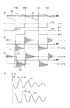
- FIG. 24 is a diagram showing a timing chart during the switching operation according to the conventional example, and shows only the operation of the high-side switching element group Q91 in FIG.
- FIG. 24A shows the voltage fluctuation between terminals of the switching element Q91a
- FIG. 24B shows the voltage fluctuation between terminals of the switching element Q91b
- FIG. 24C is an enlarged view of the portion (D).
- the on-off switching operation of the switching elements Q91a and Q91b causes the terminal voltage of each switching element to transition between a high level and a low level.
- the state transition is not simply performed between the high level and the low level.
- ringing voltages as indicated by Vra and Vrb are generated between the terminals of the switching elements Q91a and Q91b, respectively. Yes.
- This ringing voltage is resonance caused by the parasitic inductance component L and the parasitic capacitance component C included in the circuit constituting the three-phase inverter. As a result of intensive studies by the present inventors, it has been found that this ringing voltage is one of the causes of switching noise.
- the present invention has been made in view of the above problems, and an object thereof is to provide a power conversion device capable of efficiently suppressing switching noise.
- a power converter includes a capacitor, a plurality of switching elements connected in parallel to the capacitor, and a controller that individually controls a switching operation in each switching element,
- a closed circuit including any one of the plurality of switching elements and the capacitor is a power conversion device formed for each switching element, and the controller is turned on or off performed by each switching element.
- a ringing voltage generated in each closed circuit by a switching operation and having a frequency defined by an inductance included in each closed circuit and an output capacity of a switching element included in the closed circuit is generated in each of the plurality of closed circuits. So that at least two closed circuits cancel each other , Shifted from each other the timing of the switching operation in said at least two closed circuit of the switching element.
- the ringing voltage generated in the closed circuit including the capacitor and the switching element by the switching operation performed in each switching element is canceled out between the at least two closed circuits.
- “so that the ringing voltage is canceled” includes not only the case where the ringing voltage is completely canceled but also the case where the ringing voltage is partially canceled. Even when a part of the ringing voltage is canceled out, it is possible to suppress the switching noise as compared with the conventional case.
- Patent Document 1 it is conceivable to take a technique of suppressing switching noise by adding a noise canceling circuit to the power converter.
- this method can suppress the switching noise generated by the switching operation from being conducted from the closed circuit to the power supply side, the switching noise itself can be suppressed in the closed circuit. I can't. Therefore, it is effective for conduction noise transmitted to the power supply side via parasitic capacitance and wiring included in the circuit that constitutes the system, but there is a problem that the suppression effect is low for radiation noise radiated to the space. is there.
- switching noise can be suppressed in the closed circuit that is the source of the switching noise.
- it is possible to obtain an effect of suppressing radiation noise radiated to the space outside the power conversion device as well as conduction noise transmitted to the power supply via the parasitic capacitance and wiring in the power conversion device.
- FIG. 3 is a circuit diagram illustrating an example of a configuration of a phase shift unit according to the first embodiment. It is a figure which shows the timing chart which concerns on 1st Embodiment. Is a diagram showing an equivalent circuit model for calculating the frequency f r. It is a figure for demonstrating the effect which concerns on 1st Embodiment. It is a figure which shows the whole structure of 100 A of load drive systems provided with the power converter device which concerns on the modification of 1st Embodiment.
- FIG. 1 is a diagram illustrating an overall configuration of a load driving system 100 including a power conversion device according to the first embodiment.
- a configuration using a three-phase AC motor (hereinafter referred to as a motor) as a load will be described.
- the load drive system 100 includes a DC power source DC, a power converter 113, and a motor 104.
- DC power supply DC is a DC power supply obtained by rectifying a power supply system, or a DC power supply of a battery type (typically a secondary battery such as nickel metal hydride or lithium ion).
- a battery type typically a secondary battery such as nickel metal hydride or lithium ion.
- the power converter 113 includes a voltage detection unit 101, a current detection unit 103, a three-phase inverter 102, and a controller 105.
- the power conversion device 113 converts the DC power supplied from the DC power source DC into U-phase, V-phase, and W-phase three-phase AC power whose phases are 120 ° and shifted by 2 ⁇ / 3 radians in electrical angle. supplying three-phase AC power to the motor 104.
- the motor 104 is a three-phase AC motor composed of three-phase windings that are supplied with three-phase AC power.
- the voltage detection unit 101 detects the voltage of the DC power supply DC, that is, the voltage input to the three-phase inverter 102.
- the current detection unit 103 detects an input current to the motor 104, that is, a current output from the three-phase inverter 102.
- the capacitor (smoothing capacitor) 111 is provided to suppress voltage fluctuation in the power conversion device 113.
- the three-phase inverter 102 forms a three-phase bridge, and includes a U-phase arm 112u, a V-phase arm 112v, and a W-phase arm 112w.
- the configuration of the arm for each phase is the same as that of the three-phase inverter 902 in FIG.
- the switching elements Q11a and Q11b the switching elements that are connected in parallel are configured with switching elements having the same specifications such as withstand voltage and current capacity.
- the switching elements Q11a to Q16a and Q11b to Q16b include insulated gate bipolar transistors (Insulated Gate Bipolar Transistors: hereinafter referred to as IGBTs) and metal-oxide-semiconductor field effect transistors (Metal-Oxide-SemiconductorEffectTranstor: Hereinafter, a power semiconductor element represented by MOSFET is applied.
- a diode for flowing a current from the emitter side (source side) to the collector side (drain side) is connected between the collector and emitter (or between the drain and source) of the switching elements Q11a, Q11b, Q12a, and Q12b.
- MOSFET Metal-Oxide-SemiconductorEffectTranstor
- a closed circuit including any one of the switching elements Q11a to Q16a and Q11b to Q16b and the capacitor 111 is formed for each switching element.
- one closed circuit includes a switching element Q11a and a capacitor 111, and such a closed circuit is formed in the power conversion device 113 by the number of switching elements (12).
- Controller 105 The controller 105 individually controls the switching operations of the switching elements Q11a to Q16a and Q11b to Q16b included in the three-phase inverter 102.
- the controller 105 generates a pulse width modulation signal (hereinafter referred to as a PWM signal) that is a command signal to the gate drive circuit GD.
- a PWM signal a pulse width modulation signal
- the controller 105 By outputting this PWM signal to the gate terminals of the switching elements Q11a to Q16a and Q11b to Q16b via the gate drive circuit GD, each of the switching elements is individually controlled.
- the controller 105 includes a carrier signal generation unit 106, a PWM signal generation unit 107, a phase shift unit 108, a current command unit 109, and a current control unit 110.
- the carrier signal generator 106 is a carrier signal Cr that is a sawtooth voltage having a frequency of several tens of kHz (for example, the voltage gradually decreases from the first level to the second level over a predetermined time, and then from the second level to the first level). Waveform generated by repeating the reset), and outputs this to the PWM signal generator 107 at the next stage.
- the current command unit 109 outputs a current command for driving and controlling the motor 104.
- the value of the current command is set according to the target operation of the motor 104, and this command includes information on the amplitude and frequency of the control command signal to be generated by the current control unit 110 in the next stage. include.
- the current control unit 110 generates a control command signal having a sine waveform based on the current command from the current command unit 109.
- the control command signal is received as an appropriate sine waveform in response to a feedback signal from the current detection unit 103.
- the U-phase control command signal is indicated by Du
- the V-phase control command signal is indicated by Dv
- the W-phase control command signal is indicated by Dw.
- the current command unit 109 and the current control unit 110 constitute a control command signal generation unit.
- the PWM signal generation unit 107 compares the input carrier signal Cr with the U-phase control command signal Du, generates a PWM signal Pu as a comparison result, and outputs it to the phase shift unit 108 at the next stage. Similarly, carrier signal Cr and V-phase control command signal Dv, carrier signal Cr and W-phase control command signal Dw are compared, and PWM signals Pv and Pw, which are the comparison results, are generated and output to phase shift unit 108. .
- the phase shift unit 108 generates a PWM signal for each switching element based on the input PWM signals Pu, Pv, and Pw, and outputs the PWM signal to the gate drive circuit GD at the next stage.
- the phase shift unit 108 generates the PWM signal Pua by shifting the PWM signal Pu by the first phase angle, and also describes the PWM signal Pu as the second.
- the PWM signal Pub is generated by shifting by the phase angle. The second phase angle is delayed by a predetermined phase difference with respect to the first phase angle.
- the PWM signal Pua is output as a PWM signal for the switching element Q11a
- the PWM signal Pub is output as a PWM signal for the switching element Q11b.
- the phase shift unit 108 changes only the phase difference between the PWM signals Pua and Pub.
- the phase shift unit 108 performs the same phase shift on the PWM signal output to the switching elements (for example, Q14a and Q14b) connected in parallel in the other switching element groups.
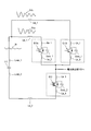
- FIG. 2 is a circuit diagram showing an example of the configuration of the phase shift unit 108, and shows the PWM signal generation unit 107 and the phase shift unit 108 taken out.
- the U-phase phase shift unit 108u includes resistors R1 and R2, capacitors C1 and C2, and Schmitt triggers Sc1 and Sc2.
- the first phase angle described above is determined by the product of R1 and C1
- the second phase angle is determined by the product of R2 and C2.
- a PWM signal Pub that is delayed by a predetermined phase difference with respect to the PWM signal Pua output from the Schmitt trigger Sc1 is generated.
- the timing of the switching operation is shifted between the switching elements Q11a and Q11b. be able to.
- the amount of deviation of the switching operation timing at this time is set to such an amount that the ringing voltage generated between the terminals of the switching element Q11a and the ringing voltage generated between the terminals of the switching element Q11b cancel each other. .
- a specific method for setting the deviation amount and its effect will be described in the next section.
- FIG. 3 is a diagram showing a timing chart according to the first embodiment. Here, only the high-side switching element group Q11 of the U-phase arm 112u will be described.
- FIG. 3A is a diagram illustrating voltage waveforms of the sawtooth carrier signal Cr and the U-phase control command signal Du input to the PWM signal generation unit 107.
- the U-phase control command signal Du has a sinusoidal waveform
- FIG. 3A is an enlarged view of a minute time, and is illustrated here as a voltage hardly changing.
- FIG. 3B shows a voltage waveform of the PWM signal Pua output from the phase shift unit 108
- FIG. 3C shows a voltage waveform of the PWM signal Pub output from the phase shift unit 108.
- the PWM signal Pub is delayed by ⁇ [sec] with respect to the PWM signal Pua, and this ⁇ corresponds to the above-described predetermined phase difference.
- R1, R2, C1, and C2 are set so that the first phase angle (product of R1 and C1) is negligible and the second phase angle (product of R2 and C2) corresponds to ⁇ .
- Such a configuration can be realized by setting a value.
- FIG. 3D shows the voltage fluctuation between the terminals of the switching element Q11a
- FIG. 3E shows the voltage fluctuation between the terminals of the switching element Q11b
- FIG. 3F shows the voltage fluctuation between FIGS.
- FIG. 3A the carrier signal Cr and the U-phase control command signal Du intersect, and the PWM signal Pua shown in FIG. 3B transitions from on to off.
- the switching element Q11a is switched from on to off, and the voltage between the terminals of the switching element Q11a transitions from a high level to a low level (FIG. 3 (d)).
- FIG. 3D since there is a large current change in the switching element Q11a in a short time, as shown in FIG. 3D, a ringing voltage Vra that is high-frequency vibration is generated between the terminals of the switching element Q11a.
- the ringing voltage generated in the switching element is one of the causes of the switching noise. Therefore, switching noise can be suppressed by suppressing the generation of the ringing voltage.
- the ringing voltage is resonance caused by the parasitic inductance component L and the parasitic capacitance component C included in the circuit constituting the three-phase inverter.
- the frequency f of the ringing voltage is determined by Equation 1.
- the PWM signal Pub shown in FIG. 3C transitions from on to off with a delay of ⁇ [sec] from time (1).
- the switching element Q11b is switched from on to off, and the voltage between the terminals of the switching element Q11b transitions from a high level to a low level (FIG. 3 (e)).
- the switching element Q11b similarly to the switching element Q11a, the switching element Q11b also has a large current change in a short time.
- the ringing voltage Vrb which is high-frequency vibration, is generated between the terminals of the switching element Q11b. appear.
- the switching elements Q11a and Q11b are configured by switching elements having the same specifications such as withstand voltage and current capacity, and the parasitic inductance L included in the switching element Q11b and The parasitic capacitance component C is the same as that included in the switching element Q11a. That is, the frequency f r of the ringing voltage Vrb generated between the frequencies f r and the switching element Q11b ringing voltage Vra terminal generated between the switching elements Q11a terminals are equivalent.
- the phase difference ⁇ is equivalent to a half cycle of ringing voltage Vra.
- ⁇ is defined by the number 2 using the frequency f r of the ringing voltage Vra.
- the frequency f r of the ringing voltage Vra is roughly the switching elements included in the inductance and the closed circuit of the closed circuit including the switching element Q11a and a capacitor 111 (closed circuit that is the source of ringing voltage Vra) It is defined by the output capacity of Q11a. The method of calculating the frequency f r of the ringing voltage Vra will be described later in detail.
- the ringing voltage Vra and the ringing voltage Vrb have a relationship in which the phases are inverted as shown in FIG. By doing so, the ringing voltages Vra and Vrb generated by the switching operation from the on to the off performed by the switching elements Q11a and Q11b cancel each other, and as a result, the switching noise generated from these switching elements is suppressed. Is done.
- the time (3) will be described.
- the carrier signal Cr and the U-phase control command signal Du intersect, and the PWM signal Pua shown in FIG. 3B transitions from off to on.
- the switching element Q11a is switched from off to on, and the voltage across the switching element Q11a transitions from low level to high level (FIG. 3 (d)).
- the ringing voltage Vra is generated between the terminals of the switching element Q11a.
- the PWM signal Pub shown in FIG. 3 (c) transitions from OFF to ON with a delay of ⁇ [sec] from time (3).
- the switching element Q11b is switched from OFF to ON, and the voltage between the terminals of the switching element Q11b transitions from low level to high level (FIG. 3 (e)).
- the ringing voltage Vrb is generated between the terminals of the switching element Q11b.
- both the ringing voltage generated in accordance with the state transition from the on state to the off state and the ringing voltage generated in accordance with the state transition from the off state to the on state can be achieved. It is possible to cancel.
- FIG. 4 is a diagram showing an equivalent circuit model for calculating the frequency f r.
- FIG. 4 illustrates only the U-phase arm 112u and the capacitor 111 in FIG.
- the switching elements Q11a and Q11b and the switching elements Q12a and Q12b are respectively connected in parallel in the U-phase arm 112u, the amount of current flowing between the switching elements Q11a and Q11b is substantially the same.
- the amount of current flowing between the switching elements Q12a and Q12b is substantially the same. Therefore, for the sake of simplification, in FIG. 4, it is assumed that the switching element of the U-phase arm 112u is composed of only the switching element Q11a and the switching element Q12a. Therefore, FIG. 4 shows a closed circuit including the switching element Q11a (or switching element Q11b) and the capacitor 111, and a closed circuit including the switching element Q12a (or switching element Q12b) and the capacitor 111.
- the capacitor 111 since the capacitor 111 is set as a sufficiently large capacity when supplying switching energy, the capacitor 111 can be regarded as an ideal voltage source. However, the capacitor 111 has a parasitic inductance component due to wiring connecting the capacitor 111 and other components, and the inductances are set as Lcap_1 and Lcap_2.
- the output capacitance of the switching element Q11 is Coss_1
- the inductances of the wiring included in the switching element Q11 are Lm_1 and Lm_2.
- the output capacitance of the switching element Q12 is Coss_2
- the inductances of the wirings connecting the switching element Q12 and other components are Lm_3 and Lm_4.
- the inductance of the wiring connecting the capacitor 111 and the U-phase arm 112u is set to Lw_1 and Lw_2.
- the inductance of the wiring included in the switching element Q11a is switched to Lm_1 and Lm_2, and the inductance included in the capacitor 111 is switched to Lcap_1 and Lcap_2.
- the inductance of the wiring connecting the element Q11a and the capacitor 111 corresponds to Lm_3, Lm_4, Lw_1, and Lw_2, respectively. Therefore, the inductance of the closed circuit including the switching element Q11a and the capacitor 111 is composed of Lcap_1, Lcap_2, Lw_1, Lw_2, Lm_1, Lm_2, Lm_3, and Lm_4.
- the inductance of the wiring included in switching element Q12a is Lm_3 and Lm_4
- the inductance included in capacitor 111 is Lcap_1 and Lcap_2
- the switching element The inductances of the wiring connecting Q12a and the capacitor 111 correspond to Lm_1, Lm_2, Lw_1, and Lw_2, respectively. Therefore, the inductance of the closed circuit including the switching element Q12a and the capacitor 111 is composed of Lcap_1, Lcap_2, Lw_1, Lw_2, Lm_1, Lm_2, Lm_3, and Lm_4.
- the equivalent circuit model shown in FIG. 4 forms a resonance circuit composed of the parasitic inductance component L and the parasitic capacitance component C.
- Frequency f r of the equivalent circuit model of FIG. 4 can be calculated by applying Equation 1 to the equivalent circuit. Indeed when calculating the frequency f r, (1) Consider the case where the switching element Q11a switching element Q12a is ON off, (2) when the switching element Q11a switching element Q12a ON is two in the case of off .
- the switching operation to turn off the switching element Q11a is a trigger, and a ringing voltage is generated between the terminals of the switching element Q11a.
- the switching element Q12a can be regarded as a simple wiring, more precisely, a resistor due to the on-resistance of the switching element. Therefore, the frequency f r1 of the ringing voltage in the case of (1) is expressed by Equation 3.
- the switching operation to turn off the switching element Q12a is a trigger, and a ringing voltage is generated between the terminals of the switching element Q12a.
- the switching element Q11a can be regarded as a simple wiring, more precisely, a resistor due to the on-resistance of the switching element. Therefore, the frequency f r2 of the ringing voltage in the case of (2) is expressed by Equation 4.
- the frequency f r is not affected by the motor 104 is determined by the capacitor 111 and the U-phase arm 112u. Be calculated each parasitic inductance components such Lm_1 and Lm_2 using an electromagnetic field simulation, etc., it is possible to obtain the frequency f r from the number 5 in the design phase. Further, when the frequency fr is obtained, the phase shift amount ⁇ [sec] of Equation 2 is also obtained. Therefore, it is possible to set the value of the predetermined phase difference ⁇ at the design stage.
- the V-phase arm 112v, W-phase arm 112w is the U-phase arm 112u and specifications are composed of the same components, V-phase arm 112v , the frequency f r of the ringing voltage generated by the switching operation in the W-phase arm 112w is as shown in Equation 5.
- FIG. 5 is a diagram for explaining the effect according to the present embodiment. 5, only the U-phase arm 112u and the capacitor 111 are shown in the same manner as FIG.
- the switching element Q11 is illustrated by distinguishing between the switching element Q11a and the switching element Q11b, but the switching element Q12 is simplified as in FIG.
- the switching elements Q11a and Q11b since the switching elements having the same specifications are used for the switching elements Q11a and Q11b, the output capacitance (Coss_1) of these switching elements and the inductance of the wiring connecting these to other components, etc. (Lm_1, Lm_2) are the same. Further, if the wiring distance connecting capacitor 111 and switching element Q11a is the same as the wiring distance connecting capacitor 111 and switching element Q11b, the inductance of these wirings can be Lw_1. Therefore, the switching elements Q11a, ringing voltage Vra generated between Q11b of terminals, the frequency f r of the Vrb is the same.
- the ringing voltages Vra and Vrb can be canceled in a closed circuit connecting the switching elements Q11a and Q11b and the capacitor 111, and are closed as indicated by Vr in FIG. voltage variations in the circuit is suppressed. Therefore, not only the conduction noise transmitted to the power supply via the parasitic capacitance and wiring in the power converter, but also the effect of suppressing radiation noise radiated to the space outside the power converter can be expected. Further, since the switching noise is suppressed in the closed circuit that is a generation source, it is possible to exert an effect of suppressing both so-called normal mode noise and common mode noise.
- noise suppression components such as an EMI filter and a shield are not used. , suppression of switching noise can be obtained. Even when a noise suppression component is used, a component having a small noise suppression effect is sufficient, and the load drive system 100 does not increase in size.
- the PWM signal generated by the PWM signal generation unit 107 is phase-shifted by the phase shift unit 108 to generate the PWM signal for each switching element.
- a carrier signal for each switching element is generated, and a PWM signal for each switching element is generated based on these signals.
- FIG. 6 is a diagram illustrating an overall configuration of a load drive system 100A including a power conversion device according to a modification of the first embodiment.
- the difference between the configuration shown in FIG. 6 and the first embodiment (FIG. 1) is the configuration of the controller 105A in the power conversion device 113A, mainly the carrier signal generation unit 106A and the PWM signal generation unit 107A.
- the description will be continued focusing on the high-side switching element group Q11 of the U-phase arm 112u.
- the carrier signal generation unit 106A generates sawtooth carrier signals Cra and Crb for generating the PWM signals Pua and Pub for the switching elements Q11a and Q11b, and outputs them to the PWM signal generation unit 107A in the next stage.
- FIG. 7 is a circuit diagram showing an example of the configuration of the carrier signal generation unit 106A according to this modification.
- the pulse signal generation unit generates a pulse signal Pl that is a narrow pulse waveform generated at a constant period, and outputs the pulse signal Pl to the phase shift circuit at the next stage.
- the phase shift circuit generates a pulse signal for each switching element based on the input pulse signal Pl.
- the phase shift circuit shifts the pulse signal Pl by the third phase angle to generate the pulse signal Pl1, and shifts the pulse signal Pl by the fourth phase angle to generate the pulse signal Pl2.
- the fourth phase angle is delayed by ⁇ [sec] with respect to the third phase angle.
- the pulse signal Pl1 is output to the transistor Tr1, and the pulse signal Pl2 is output to the transistor Tr2.
- Transistors Tr1 and Tr2 are turned on for a moment in a constant cycle when pulse signals Pl1 and Pl2 are input. Further, since the pulse signal Pl2 is delayed by ⁇ [sec] relative to the pulse signal Pl1, the timing at which the transistor Tr2 is turned on is also delayed by ⁇ [sec] relative to the transistor Tr1.
- the capacitor C3 is discharged toward the constant current source I, and the voltage of the capacitor C3 drops at a constant speed.
- the capacitor C3 is charged, and the voltage of the capacitor C3 increases instantaneously at a constant period.
- circuit configuration shown in FIG. 7 for example, the circuit configuration disclosed in FIG. 3 of Patent Document 2 can be used.
- PWM signal generation unit 107A (FIG. 6) generates PWM signal Pu for switching element Q11a and PWM signal Pub for switching element Q11b based on carrier signals Cra and Crb.
- the PWM signals Pua and Pub finally output to the switching elements Q11a and Q11b are the same as the PWM signals Pua and Pub (FIGS. 3B and 3C) in the first embodiment.
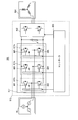
- FIG. 8 is a diagram illustrating a partial configuration of the power conversion device according to the second embodiment, in particular, a three-phase inverter 202 and a phase shift unit 208.
- the three-phase inverter 202 includes a high-side switching element group Q21, Q23, Q25 and a low-side switching that constitute a U-phase arm 212u, a V-phase arm 212v, and a W-phase arm 212w.
- a high-side switching element group Q21, Q23, Q25 and a low-side switching that constitute a U-phase arm 212u, a V-phase arm 212v, and a W-phase arm 212w.
- a plurality of switching elements are connected in parallel. However, the number of switching elements connected in parallel is different from that of the first embodiment.
- the high-side switching element group Q21 includes three switching elements Q21a, Q21b, and Q21c connected in parallel
- the low-side switching element group Q22 includes a switching element.
- Three switching elements Q22a, Q22b, and Q22c are connected in parallel.
- the high-side switching element group Q23 of the V-phase arm 212v has three switching elements Q23a, Q23b, and Q23c
- the low-side switching element group Q24 has switching elements Q24a and Q24b. , Q24c are connected in parallel.
- the high-side switching element group Q25 includes three switching elements Q25a, Q25b, and Q25c
- the low-side switching element group Q26 includes three switching elements Q26a, Q26b, and Q26c. Each of the switching elements is connected in parallel.
- the phase shift unit 208 has substantially the same configuration as that of the phase shift unit 108 according to the first embodiment, and the configuration not particularly shown in FIG. 8 is also substantially the same as that of the first embodiment.
- the description will focus on the high-side switching element group Q21 of the U-phase arm 212u.
- the phase shift unit 208 is based on the PWM signal Pu input from the PWM signal generation unit (not shown), the PWM signal Pua for the switching element Q21a, the PWM signal Pub for the switching element Q21b, and the PWM signal for the switching element Q21c.
- Puc is generated and output to the gate drive circuit GD at the next stage.
- the phase shift unit 208 shifts the PWM signal Pu by the first phase angle to generate the PWM signal Pua, shifts the PWM signal Pu by the second phase angle to generate the PWM signal Pub, and generates the PWM signal Pu.
- the PWM signal Puc is generated by shifting by the third phase angle.
- the second phase angle is delayed by ⁇ [sec] (same as described in the first embodiment) with respect to the first phase angle
- the third phase angle is equal to the second phase angle. It is delayed by ⁇ [sec] with respect to the phase angle.
- the timing of the switching operation can be shifted between the switching elements Q21a, Q21b, and Q21c.
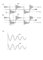
- FIG. 9 is a diagram illustrating a timing chart according to the second embodiment. Here, only the high-side switching element group Q21 of the U-phase arm 212u will be described.
- FIG. 9A is a diagram illustrating voltage waveforms of the sawtooth carrier signal Cr and the U-phase control command signal Du input to the PWM signal generation unit according to the present embodiment. These voltage waveforms are the first waveform. This is the same as that according to the embodiment (FIG. 3A).
- FIG. 9B shows the voltage waveform of the PWM signal Pua output from the phase shift unit 208
- FIG. 9C shows the voltage waveform of the PWM signal Pub
- FIG. 9D shows the voltage waveform of the PWM signal Puc. Show.
- the PWM signal Puc is 2 ⁇ [sec] with respect to the PWM signal Pua ( ⁇ is the same as that described in the first embodiment). It is delayed by ⁇ [sec] with respect to the PWM signal Pub.
- FIG. 9E shows the voltage fluctuation between the terminals of the switching element Q21a
- FIG. 9F shows the voltage fluctuation between the terminals of the switching element Q21b
- FIG. 9G shows the voltage between the terminals of the switching element Q21c.
- FIG. 9 (h) shows an enlarged view around (B) shown in FIGS. 9 (e), (f), and (g).
- time (1) in FIG. 9 will be described.
- the carrier signal Cr and the U-phase control command signal Du cross each other, and the PWM signal Pua shown in FIG. 9B transitions from on to off.
- the switching element Q21a is switched from on to off, and the voltage between the terminals of the switching element Q21a transitions from the high level to the low level (FIG. 9 (e)).
- a ringing voltage Vra is generated between the terminals of the switching element Q21a.
- FIG. 9 (2) a description will be given time in FIG. 9 (2).
- the PWM signal Pub shown in FIG. 9C transitions from on to off with a delay of ⁇ [sec] from time (1).
- the switching element Q21b is switched from on to off, and the voltage between the terminals of the switching element Q21b transitions from a high level to a low level (FIG. 9 (f)).
- a ringing voltage Vrb is generated between the terminals of the switching element Q21b.
- the ringing voltage Vra and the ringing voltage Vrb have a relationship in which the phases are inverted.
- the ringing voltages Vra and Vrb generated by the switching operation from on to off performed by the switching elements Q21a and Q21b cancel each other, and as a result, switching noise generated from these switching elements is suppressed. Is done.
- the PWM signal Puc shown in FIG. 9D transitions from on to off with a delay of ⁇ [sec] from time (2) and 2 ⁇ [sec] from time (1).
- the switching element Q21c is switched from on to off, and the voltage between the terminals of the switching element Q21c transitions from the high level to the low level (FIG. 9 (g)).
- a ringing voltage Vrc is generated between the terminals of the switching element Q21c. This ringing voltage Vrc remains as it is without canceling out other ringing voltages.
- the time (4) will be described.
- the carrier signal Cr and the U-phase control command signal Du intersect, and the PWM signal Pua shown in FIG. 9B transitions from OFF to ON.
- the switching element Q21a is switched from OFF to ON, and the voltage between the terminals of the switching element Q21a transitions from the low level to the high level ((e) in FIG. 9).
- the ringing voltage Vra is generated between the terminals of the switching element Q21a.
- the PWM signal Pub shown in FIG. 9 (c) transitions from OFF to ON with a delay of ⁇ [sec] from time (4).
- the switching element Q21b is switched from off to on, and the voltage across the terminals of the switching element Q21b transitions from low level to high level (FIG. 9 (f)).
- the ringing voltage Vrb is generated between the terminals of the switching element Q21b.
- the PWM signal Puc shown in FIG. 9D transitions from OFF to ON with a delay of ⁇ [sec] from time (5) and 2 ⁇ [sec] from time (4).
- the switching element Q21c is switched from OFF to ON, and the voltage between the terminals of the switching element Q21c transitions from low level to high level (FIG. 9 (g)).
- the ringing voltage Vrc is generated between the terminals of the switching element Q21c. This ringing voltage Vrc remains as it is without canceling out other ringing voltages.
- the ringing voltages Vra and Vrb are generated when the switching element is generated along with the state transition from on to off, and with the state transition from off to on. It is possible to cancel both of the occurrences.
- the switching noise suppression effect is inferior to that of the first embodiment.
- the switching noise can be suppressed to about one third as compared with the conventional case where three switching elements are operated in synchronization.
- phase shift unit Similar to the phase shift unit 208 according to the second embodiment, the phase shift unit according to the present modification generates the PWM signals Pua, Pub, and Puc. In the second embodiment, a predetermined phase difference is generated. Is ⁇ [sec], in the present modification, this predetermined phase difference is ⁇ [sec]. ⁇ is defined by the number 6 using the frequency f r of the ringing voltage generated in the switching element.
- phase difference ⁇ corresponds to one-third period of the ringing voltage.
- FIG. 10 is a diagram illustrating a timing chart according to the present modification.
- FIGS. 10A, 10B, and 10C illustrate ringing voltages Vra, Vrb, and Vrc generated in the switching elements Q21a, Q21b, and Q21c, respectively. it is an enlarged view of the waveform.
- the phase difference ⁇ By setting the phase difference ⁇ to a value corresponding to one-third period of the ringing voltage, when the ringing voltages Vra, Vrb, and Vrc are accurate sine waves, the sum of these ringing voltages is zero. And the ringing voltages cancel each other.
- FIG. 11 is a diagram illustrating an overall configuration of a load driving system 300 including the power conversion device according to the third embodiment.
- the load driving system 300 includes a DC power source DC, a power conversion device 313, and a motor 304.
- the direct-current power source DC and the motor 304 have the same configuration as the direct-current power source DC and the motor 104 in the first embodiment, respectively, but the configuration of the power conversion device 313 is different from that of the power conversion device 113 in the first embodiment.
- the power conversion device 313 includes a voltage detection unit 301, a current detection unit 303, a three-phase inverter 302, and a controller 305.
- the voltage detection unit 301 and the current detection unit 303 have the same configuration as the voltage detection unit 101 and the current detection unit 103 in the first embodiment, respectively.
- the three-phase inverter 302 and the controller 305 are different in configuration from the three-phase inverter 102 and the controller 105 in the first embodiment.
- the three-phase inverter 302 includes a U-phase arm 312u, a V-phase arm 312v, and a W-phase arm 312w.
- the U-phase arm 312u further includes a high-side switching element Q31 and a low-side switching element Q32 connected in series.
- the high-side switching element Q31 and the low-side switching element Q32 of this embodiment are each composed of a single switching element.
- the V-phase arm 312v and the W-phase arm 312w have the same configuration as the U-phase arm 312u.
- the switching elements Q31 to Q36 are constituted by a common switching element.
- a closed circuit including any one of the U-phase arm 312u, the V-phase arm 312v, and the W-phase arm 312w and the capacitor 311 is formed for each arm. That is, one closed circuit includes a U-phase arm 312u and a capacitor 311. Such a closed circuit is formed in the power conversion device 313 by the number of arms (three).
- the description will focus on the high-side switching elements Q31, Q33, and Q35.
- the controller 305 includes a carrier signal generation unit 306, a PWM signal generation unit 307, a phase shift unit 308, a current command unit 309, and a current control unit 310.
- the carrier signal generation unit 306, the PWM signal generation unit 307, the current command unit 309, and the current control unit 310 are the carrier signal generation unit 106, the PWM signal generation unit 107, the current command unit 109, and the current control, respectively, in the first embodiment. parts 110 have the same configuration as.
- the phase shift unit 308 is different in configuration from the phase shift unit 108 in the first embodiment.
- the phase shift unit 308 includes a PWM signal Pu ′ output to the high side switching element Q31 based on the input PWM signals Pu, Pv, and Pw, a PWM signal Pv ′ output to the high side switching element Q33, and the high side switching element.
- the PWM signal Pw ′ output to Q35 is generated and output to the next stage gate drive circuit GD.
- the phase shift unit 308 shifts the PWM signal Pu by the first phase angle to generate the PWM signal Pu ′, shifts the PWM signal Pv by the second phase angle to generate the PWM signal Pv ′, and generates the PWM signal.
- the PWM signal Pw ′ is generated by shifting Pw by the third phase angle.
- the second phase angle is delayed by ⁇ [sec] (same as described in the first embodiment) with respect to the first phase angle
- the third phase angle is equal to the second phase angle. It is delayed by ⁇ [sec] with respect to the phase angle.
- the frequency of the ringing voltage generated in the closed circuit including the U-phase arm 312u and the capacitor 311 by the switching operation of the switching element Q31 of the U-phase arm 312u is included in the inductance included in the closed circuit and the closed circuit. It is defined by the output capacity of the switching element Q31 constituting the arm.
- FIG. 4 shows a closed circuit including U-phase arm 312u and capacitor 311. Therefore, the method for calculating the frequency fr described in FIG. 4 can also be applied to this embodiment.
- the switching element Q31 and the capacitor 311 are connected to the inductance of the wiring included in the switching element Q31 with Lm_1 and Lm_2, and the inductance included in the capacitor 311 with Lcap_1 and Lcap_2.
- the wiring inductances correspond to Lm_3, Lm_4, Lw_1, and Lw_2, respectively. Therefore, the inductance included in this closed circuit is composed of Lcap_1, Lcap_2, Lw_1, Lw_2, Lm_1, Lm_2, Lm_3, and Lm_4.
- FIG. 12A is a diagram illustrating voltage waveforms of the sawtooth carrier signal Cr, the U-phase control command signal Du, the V-phase control command signal Dv, and the W-phase control command signal Dw input to the PWM signal generation unit 307.
- the carrier signal Cr has a sawtooth waveform similar to that in the first embodiment.
- the U-phase control command signal Du, V-phase control command signal Dv, and W-phase control command signal Dw are 120 ° out of phase and 2 ⁇ / 3 radians at an electrical angle.
- FIG. 12B shows a voltage waveform of the PWM signal Pu ′ output from the phase shift unit 308.
- FIG. 12C shows the voltage waveform (dotted line) of the PWM signal Pv input to the phase shift unit 308 and the PWM signal Pv ′ (solid line) output from the phase shift unit 308, respectively.
- the PWM signal Pv ′ is delayed by ⁇ [sec] with respect to the PWM signal Pv.
- FIG. 12D shows the voltage waveform (dotted line) of the PWM signal Pw input to the phase shift unit 308 and the PWM signal Pw ′ (solid line) output from the phase shift unit 308, respectively.
- the PWM signal Pw ′ is delayed by 2 ⁇ [sec] with respect to the PWM signal Pw.
- FIG. 12 (e) shows the voltage fluctuation between the terminals of the high-side switching element Q31
- FIG. 12 (f) shows the voltage fluctuation between the terminals of the high-side switching element Q33
- FIG. 12 (g) shows the high-side switching element.
- FIG. 12 (h) shows an enlarged view of the vicinity of (C) shown in FIGS. 12 (e), 12 (f), and 12 (g).
- FIG. 12A the carrier signal Cr and the U-phase control command signal Du cross each other, and the PWM signal Pu ′ shown in FIG. 12B transitions from on to off.
- the high-side switching element Q31 is switched from on to off, and the voltage between the terminals of the high-side switching element Q31 transitions from the high level to the low level (FIG. 12 (e)).
- a ringing voltage Vru is generated between the terminals of the high-side switching element Q31.
- the control command signals Dv and Dw also intersect with the carrier signal Cr at time (1), and thus are output from the PWM signal generation unit 307. Also in the PWM signals Pv and Pw, the state transition from on to off occurs. If the PWM signals Pv and Pw are output to the gate terminals of the high-side switching elements Q33 and Q35 without being phase-shifted by the phase shift unit 308, the high-side switching elements Q31, Q33, and Q35 are simultaneously switched. Will be done. As a result, ringing voltages having the same phase are generated from the high-side switching elements Q31, Q33, and Q35, so that switching noise is superimposed in triplicate. Therefore, in this embodiment, the phase shift unit 308 is configured to shift the phases of the PWM signals Pv and Pw so that the switching operation is not performed at the same time.
- the PWM signal Pv ′ output from the phase shift unit 308 has a phase difference of ⁇ [sec] with respect to the PWM signal Pv (FIG. 12C).
- ⁇ is defined by Equation 2 in the first embodiment.
- the frequency f r in equation 2 is the frequency of the ringing voltage Vru occurring high-side switching element Q31.
- the switching elements Q31 to Q36 are composed of switching elements having the same specifications such as withstand voltage and current capacity, the frequency of the ringing voltage generated in each switching element is the same value.
- the PWM signal Pv ′ shown in FIG. 12 (c) is changed from on to off with a delay of ⁇ [sec] from time (1).
- the high-side switching element Q33 is switched from on to off, and the voltage between the terminals of the high-side switching element Q33 transitions from the high level to the low level (FIG. 12 (f)).
- a ringing voltage Vrv is generated between the terminals of the high-side switching element Q33.
- the ringing voltage Vru and the ringing voltage Vrv have a relationship in which the phases are inverted.
- the ringing voltages Vru and Vrv generated in association with the switching operation from on to off performed by the high-side switching elements Q31 and Q33 are canceled out, and as a result, switching noise generated from these switching elements. Is suppressed.
- time (3) in FIG. 12 will be described.
- the PWM signal Pw ′ shown in FIG. 12 (d) is shifted from on to off with a delay of 2 ⁇ [sec] from time (1).
- the high-side switching element Q35 is switched from on to off, and the voltage between the terminals of the high-side switching element Q35 transitions from the high level to the low level (FIG. 12 (g)).
- a ringing voltage Vrw is generated between the terminals of the high-side switching element Q35.
- This ringing voltage Vrw remains as it is without canceling out other ringing voltages.
- the ringing voltages Vru and Vrv can be canceled with each other when the switching element is generated with the state transition from on to off.
- the switching noise suppression effect is inferior compared with the first embodiment.
- the switching noise is suppressed to about one third as compared with the case where all the switching elements of the U phase, the V phase, and the W phase are simultaneously switched. Is possible.
- the carrier signal is set to a predetermined time, such as a sawtooth wave, for example. It is preferable to use a carrier signal that repeats reset from the second level to the first level after transition from the first level to the second level.
- a carrier signal that repeats reset from the second level to the first level after transition from the first level to the second level.
- the time at which the switching operation is performed simultaneously occurs periodically corresponding to the timing at which the carrier signal is reset, and does not vary with the duty ratio.
- the timing of the switching operation in the switching element of each phase is controlled by using this time as a phase shift reference. It is possible.
- the switching element cancels both the ringing voltage generated in accordance with the state transition from on to off and the ringing voltage generated in accordance with the state transition from off to on. It was possible to do.
- the ringing voltage that can be canceled is limited to either one. This is because, as shown in FIGS. 12B to 12D, the timing at which the carrier signal and the control command signal intersect in the period in which the carrier signal transitions from the first level to the second level over a predetermined time. This is because it varies depending on the duty ratio. Therefore, it is difficult to use the timing at which the carrier signal and the control command signal intersect as the phase shift reference. However, since either one of the ringing voltages can be canceled out, the noise level can be suppressed to about half compared to the case where the PWM signal for each phase is not phase-shifted.
- a carrier signal for each phase in which a predetermined phase difference is provided between the phases is generated in advance, and each phase is based on the carrier signals. It is also possible to adopt a configuration for generating a PWM signal for use.
- the verification of the switching noise suppression principle according to the present embodiment was specifically performed using the circuit shown in FIG.
- the principle verification circuit shown in FIG. 13 is based on the circuit configuration shown in FIG. 11, and the same components as those shown in FIG.
- a pulse signal is sent from the pulse generator 321 to the gate terminals of the high-side switching elements Q31 and Q33.
- the high-side switching elements Q31 and Q33 perform a switching operation.
- the pulse signal output from the pulse generator 321 has a time difference between the high-side switching elements Q31 and Q33, and the timing of the switching operation is thereby shifted.
- a load 320 is connected to the U-phase arm and the V-phase arm.
- FIG. 14 (a) is a result of assuming the switching operation of the present embodiment
- FIG. 14 (b) is a result of a comparative example.
- the voltage fluctuation between the terminals of the low side switching element Q32 is indicated by a solid line
- the voltage fluctuation between the terminals of the low side switching element Q34 is indicated by a dotted line.
- the time difference between the pulse signals input to the high-side switching elements Q31 and Q33 is ⁇ [sec], and the phase of the ringing voltage is inverted with respect to each other. Yes.
- the time difference between the input pulse signals is substantially zero, and the phase of the ringing voltage is substantially the same.
- a pseudo power supply network (LISN) 318 (FIG. 13) is connected between the DC power supply DC and the three-phase inverter, and voltage fluctuations as shown in FIG. 14 occur between the terminals of the low-side switching elements Q32 and Q34.
- the noise spectrum was measured by the spectrum analyzer 319, and the result is shown in FIG.
- the solid line in FIG. 15 is the result in the present embodiment (corresponding to FIG. 14A), and the dotted line is the result in the comparative example (corresponding to FIG. 14B).
- the switching elements with which the ringing voltages are canceled are switching elements of different phases. Therefore, the PWM signals input to these switching elements are generated based on control command signals having different phases.
- the switching elements that cancel out the ringing voltages are switching elements in the same phase. Therefore, the PWM signal input to these switching elements is generated based on the same control command signal. Therefore, as in the case of the first and second embodiments and the modifications thereof, the embodiment in which the ringing voltages are canceled out between the switching elements in the same phase achieves more accurate noise suppression. Is possible.
- the phase shift unit Similar to the phase shift unit 308 according to the third embodiment, the phase shift unit according to the present modification generates the PWM signals Pu ′, Pv ′, and Pw ′.
- the phase shift unit is predetermined.
- the predetermined phase difference is ⁇ [sec] in the present modification.
- the ⁇ is defined by the number 6 using the frequency f r of the ringing voltage in the same manner as in the modification of the second embodiment, generated in the switching element.
- the frequency f r in equation 6 is the frequency of the ringing voltage Vru occurring high-side switching element Q31.
- this phase difference ⁇ corresponds to one-third period of the ringing voltage.
- FIG. 16 is a diagram illustrating a timing chart according to the present modification.
- FIGS. 16A, 16B, and 16C are ringing voltages Vru and Vrv generated in the high-side switching elements Q31, Q33, and Q35, respectively. , Vrw waveform enlarged view.
- the phase difference ⁇ By setting the phase difference ⁇ to a value corresponding to one third of the ringing voltage, when the ringing voltages Vru, Vrv, and Vrw are accurate sine waves, the sum of these ringing voltages is zero. And the ringing voltages cancel each other.
- FIG. 17 is a diagram illustrating an overall configuration of a load driving system 400 including a power conversion device according to the fourth embodiment. A fourth embodiment will be described with reference to FIG.
- the load drive system 400 includes a DC power source DC, a power conversion device 413, and a motor 404.
- the DC power source DC and the motor 404 have the same configuration as the DC power source DC and the motor 304 in the third embodiment (FIG. 11), respectively, but the power conversion device 413 is the same as the power conversion device 313 in the third embodiment. The configuration is different.
- the power converter 413 includes a voltage detection unit 401, a current detection unit 403, a three-phase inverter 402, and a controller 405.
- the voltage detection unit 401 and the controller 405 are different in configuration from the voltage detection unit 301 and the controller 305 in the third embodiment.
- the controller 405 includes a carrier signal generation unit 406, a PWM signal generation unit 407, a phase shift unit 408, a current command unit 409, and a current control unit 410.
- the carrier signal generation unit 406, the PWM signal generation unit 407, the current command unit 409, and the current control unit 410 are respectively the carrier signal generation unit 306, the PWM signal generation unit 307, the current command unit 309, and the current control in the third embodiment.
- the configuration is the same as that of the unit 310.
- the phase shift unit 408 is different in configuration from the phase shift unit 308 in the third embodiment.
- the difference between the load driving system 400 according to the present embodiment and the third embodiment is that the voltage value of the DC power source DC detected by the voltage detection unit 401 is added as an input to the phase shift unit 408.
- the frequency of the ringing voltage is determined by the output capacity C of the switching element from Equation 1, but it is known that the output capacity of the switching element decreases as the voltage between the terminals of the switching element increases. Therefore, the frequency of the ringing voltage increases as the power supply voltage value increases as noise based on the ringing voltage is conducted from the three-phase inverter 402 to the DC power supply DC side. Therefore, in order to obtain a good noise suppression effect in a system in which the power supply voltage varies greatly, it is necessary to make the set value of the phase difference in the phase shift unit variable.
- the set value of the phase difference provided in the phase shift unit 408 is made variable according to the power supply voltage value detected by the voltage detection unit 401. This can be performed by a method in which a set value of a phase difference corresponding to the power supply voltage value detected by the voltage detection unit 401 is prepared as a database in advance.
- the phase shift unit 408 obtains a feedback signal based on the power supply voltage value detected by the voltage detection unit 401, reads a set value of a phase difference corresponding to the signal from the database, and performs a phase shift operation.
- FIG. 18 is a diagram illustrating an overall configuration of a load driving system 500 including a power conversion device according to the fifth embodiment. The fifth embodiment will be described with reference to FIG.
- the load drive system 500 includes a DC power source DC, a power converter 513, and a motor 504.
- the direct current power source DC and the motor 504 have the same configuration as the direct current power source DC and the motor 404 in the fourth embodiment (FIG. 17), respectively, but the power conversion device 513 is the same as the power conversion device 413 in the fourth embodiment. The configuration is different.
- the power converter 513 includes current detectors 501 and 503, a three-phase inverter 502, and a controller 505.
- the current detection unit 503 and the three-phase inverter 502 have the same configuration as the current detection unit 403 and the three-phase inverter 402 in the fourth embodiment, respectively.
- the controller 505 has a different configuration from the controller 405 in the fourth embodiment, and the current detection unit 501 has a configuration that does not exist in the fourth embodiment.
- the controller 505 includes a carrier signal generation unit 506, a PWM signal generation unit 507, a phase shift unit 508, a current command unit 509, and a current control unit 510.
- the carrier signal generation unit 506, the PWM signal generation unit 507, the current command unit 509, and the current control unit 510 are respectively the carrier signal generation unit 406, the PWM signal generation unit 407, the current command unit 409, and the current control in the fourth embodiment.
- the configuration is the same as that of the unit 410.
- the phase shift unit 508 is different in configuration from the phase shift unit 408 in the fourth embodiment.
- the difference between the load driving system 500 according to the present embodiment and the fourth embodiment is that the current value of the DC power source DC detected by the current detection unit 501 is input to the phase shift unit 508.
- Current detecting section 501 is provided with a high-pass filter, for detecting a ringing voltage component that conducts to the DC power supply DC side from the three-phase inverter 502.
- the frequency of the ringing voltage is calculated by determining the zero crossing of the ringing voltage component, and the set value of the phase difference is determined from Equation 2 or Equation 6 based on the frequency of the ringing voltage.
- the phase shift unit 508 performs a phase shift operation based on the phase difference determined in this way.
- an efficient noise suppression effect can be obtained even in a system in which the frequency band of the ringing voltage varies.
- FIG. 19 is a diagram illustrating an overall configuration of a load driving system 600 including the power conversion device according to the sixth embodiment. The sixth embodiment will be described with reference to FIG.
- the load drive system 600 includes a DC power source DC, a power conversion device 613, and a motor 604.
- the direct current power source DC and the motor 604 have the same configuration as the direct current power source DC and the motor 504 in the fifth embodiment (FIG. 18), respectively, but the power conversion device 613 is the same as the power conversion device 513 in the fifth embodiment. The configuration is different.
- the power converter 613 includes a voltage detection unit 601, a current detection unit 603, a three-phase inverter 602, and a controller 605.
- the voltage detection unit 601 and the three-phase inverter 602 have the same configuration as the current detection unit 301 in the third embodiment and the three-phase inverter 502 in the fifth embodiment, respectively.
- the current detection unit 603 and the controller 605 are different in configuration from the current detection unit 503 and the controller 505 in the fifth embodiment.
- the controller 605 includes a carrier signal generation unit 606, a PWM signal generation unit 607, a phase shift unit 608, a current command unit 609, and a current control unit 610.
- the carrier signal generation unit 606, the PWM signal generation unit 607, the current command unit 609, and the current control unit 610 are respectively the carrier signal generation unit 506, the PWM signal generation unit 507, the current command unit 509, and the current control in the fifth embodiment.
- the configuration is the same as that of the unit 510.
- the phase shift unit 608 is different in configuration from the phase shift unit 508 in the fifth embodiment.
- the current of the DC power source DC that is, the input current value of the three-phase inverter 502 is input to the phase shift unit 508 has been described.
- the three-phase inverter 602 The difference is that the output current value is input to the phase shift unit 608.
- Current detecting section 603 is provided with a high-pass filter, for detecting a ringing voltage component conducted from the three-phase inverter 602 to the motor 604 side.
- the frequency of the ringing voltage is calculated by determining the zero crossing of the ringing voltage component, and the set value of the phase difference is determined from Equation 2 or Equation 6 based on the frequency of the ringing voltage.
- the phase shift unit 608 performs a phase shift operation based on the phase difference determined in this way.
- an efficient noise suppression effect can be obtained even in a system in which the frequency band of the ringing voltage varies. Furthermore, in the present embodiment, since the current value on the output side of the three-phase inverter 602 is detected, unlike the fifth embodiment, the output current value is detected for each of the U phase, the V phase, and the W phase. It is possible. The present embodiments are, therefore, the frequency of the ringing voltage can be said to be effective when the U-phase, V-phase, W-phase at different like.
- the PWM method for controlling the output voltage by changing the current flow rate of each switching element constituting the three-phase inverter has been described, but the present invention is not limited to this.
- a drive system in which a chopper circuit is connected between a DC power supply and a three-phase inverter, and the input voltage of the motor is variably controlled by varying the output voltage of the chopper circuit so-called PAM (Pulse Amplitude Modulation) system.
- PAM Pulse Amplitude Modulation
- FIG. 20 is a diagram illustrating an overall configuration of a load driving system 700 including the power conversion device according to the present embodiment.
- the load drive system 700 includes a DC power source DC, a power conversion device 713, and a motor 704.
- DC power source DC is a DC power source obtained by rectifying a power system or a battery type DC power source.
- the power conversion device 713 includes a step-up chopper circuit 716, a three-phase inverter 702, and a controller 705.
- the power conversion device 713 converts the power supplied from the DC power source DC into U-phase, V-phase, and W-phase three-phase AC power. Supply power.
- the step-up chopper circuit 716 boosts the voltage of the DC power source DC and outputs the boosted DC voltage to the three-phase inverter 702.
- the step-up chopper circuit 716 has a general configuration including an inductor 714, a diode 715, a switching element group Q7, and a capacitor 711.
- the switching element group Q7 is configured by connecting switching elements Q7a and Q7b in parallel for the purpose of increasing the amount of current that can be passed through the switching element group Q7, similarly to the switching element groups of the first and second embodiments. ing.
- a gate drive circuit GD is connected to the gate terminals of the switching elements Q7a and Q7b.
- the three-phase inverter 702 converts the power output from the step-up chopper circuit 716 into three-phase AC power and feeds it to the motor 704. Although the detailed configuration of the three-phase inverter 702 is not illustrated, the three-phase inverter 702 is configured by a three-phase bridge similarly to the three-phase inverter 302 in the third embodiment.
- the controller 705 generates a PWM signal that is a command signal to the gate drive circuit GD. By outputting this PWM signal to the gate terminals of the switching elements Q7a and Q7b via the gate drive circuit GD, each switching element is individually controlled.
- the controller 705 also generates a command signal for the three-phase inverter 702.
- the motor 704 is a three-phase AC motor including three-phase windings that are supplied with three-phase AC power from the three-phase inverter 702.
- the controller 705 in the present embodiment generates a PWM signal such that the operation timings of the switching elements Q7a and Q7 are shifted from each other in order to cancel the ringing voltages generated from the switching elements Q7a and Q7b. Since the specific operation of the controller 705 for generating the PWM signal is the same as that of the controller 105 in the first embodiment, the description thereof is omitted here.
- the switching element group Q7 is composed of two switching elements, but the number is not limited to this and may be composed of three switching elements. In that case, the structure of 2nd Embodiment and its modification can be employ
- FIG. 21 is a diagram illustrating an overall configuration of a load driving system 800 including the power conversion device according to the present embodiment.
- the load drive system 800 is a load drive system including a converter / inverter type power converter, and includes a three-phase AC power source AC, a power converter 813, and a motor 804.
- the three-phase AC power supply AC outputs U-phase, V-phase, and W-phase AC powers whose phases are 120 ° each and shifted by 2 ⁇ / 3 radians in electrical angle.
- the power converter 813 includes a three-phase converter 817, a three-phase inverter 802, a controller 805, and a capacitor 811. After rectifying the three-phase AC power supplied from the three-phase AC power source AC into DC power, the U-phase, V It is converted into three-phase AC power of phase and W phase and supplied to the motor 804.
- the three-phase converter 817 rectifies the three-phase AC power supplied from the three-phase AC power source AC into DC power, and includes a three-phase bridge of a U-phase arm 817u, a V-phase arm 817v, and a W-phase arm 817w.
- the U-phase arm 817u includes a high-side switching element Q81 and a low-side switching element Q82 connected in series, and the V-phase arm 817v and the W-phase arm 817w are similarly connected in series to the high-side switching element Q83 and the low-side switching element Q84. , High side switching element Q85 and low side switching element Q86.
- a gate drive circuit GD is connected to each gate terminal of the switching elements Q81 to Q86.
- the three-phase inverter 802 converts the DC power output from the three-phase converter 817 into three-phase AC power and supplies this to the motor 804. Although a detailed configuration of the three-phase inverter 802 is not illustrated, the three-phase inverter 802 is configured by a three-phase bridge similarly to the three-phase inverter 302 in the third embodiment.
- the controller 805 generates a PWM signal that is a command signal to the gate drive circuit GD. By outputting this PWM signal to the gate terminals of the switching elements Q81 to Q86 via the gate drive circuit GD, each switching element is individually controlled.
- the controller 805 also generates a command signal for the three-phase inverter 802.
- the capacitor 811 is provided to suppress voltage fluctuation in the power converter 813.
- the controller 805 generates U-phase, V-phase, and W-phase PWM signals by comparing the carrier signal and the control command signal.
- the third embodiment As described above, when using a carrier signal that repeats reset from the second level to the first level after transitioning from the first level to the second level over a predetermined time like a sawtooth wave, noise increases. Problems arise. This is because the superposition of the ringing voltage due to simultaneous switching operations between the switching elements of the U phase, V phase, and W phase described in the third embodiment also occurs in the three-phase converter 817.
- the controller 805 in this embodiment cancels the ringing voltages generated from the U-phase, V-phase, and W-phase switching elements, and between the switching elements Q81, Q82, and Q83 and the switching element Q84.
- PWM signals are generated such that the operation timings between Q85 and Q85 and Q86 are shifted from each other. Since the specific operation of the controller 805 for generating the PWM signal is the same as that of the controller 305 in the third embodiment and its modification, the description thereof is omitted here.
- the high-side switching element is taken up and the principle of noise suppression is explained.
- the low-side switching element can be similarly explained by reversing on and off. .
- the phase difference ⁇ is a half cycle of the ringing voltage, that is, 0.5 cycle.
- the phase difference ⁇ is 1.5 cycles. If the delay amount is 0.5 ⁇ N (N is a positive odd number) as in 2.5 cycles, the ringing voltages can be canceled with each other, so that a noise suppression effect can be obtained. is there. However, in this case, since the ringing for the delayed period remains without being canceled, the noise suppression effect is low compared to the configuration in which the phase difference ⁇ is 0.5 period.
- the example of delaying the timing of the switching operation of the switching element Q11b with respect to the switching element Q11a has been described. However, the switching operation of the switching element Q11b with respect to the switching element Q11a The same noise suppression effect can be obtained by advancing the timing.
- the phase difference ⁇ is described as a half period of the ringing voltage, or the phase difference ⁇ is described as one third of the ringing voltage.
- the phase differences ⁇ and ⁇ do not need to be exactly a half cycle and a third cycle, and may be about a half cycle and a third cycle.
- the range of “substantially half cycle” or “approximately one third cycle” indicates that the noise level when the noise suppression effect by canceling the ringing voltage is exerted is less than half the noise level in the conventional configuration.
- the “conventional configuration” here refers to a configuration in which switching elements connected in parallel are operated in synchronization as shown in FIG. A specific example will be described with reference to FIG.
- Figure 22 is a simulation of the noise level when the waveform of the ringing voltage is assumed to be accurate sine wave.
- the simulation was performed using a second sine wave having the same amplitude and frequency as the first sine wave and having a phase shifted by 180 ° (inverted phase). While shifting the phase of the second sine wave by 10% (18 °), both sine waves were added.
- the second sine wave whose phase is shifted by 10% (18 °) from the first sine wave is “10% shifted” (solid line) and 20% (36 °) is shifted. “20% deviation” (dotted line), 30% (54 °) deviation is “30% deviation” (one-dot chain line), 40% (72 °) deviation is “40% deviation” (two-dot chain line) ).
- the noise level in the conventional configuration is indicated by a broken line. Needless to say, when the phase of the second sine wave is not shifted, the summation with the first sine wave is zero level.
- the transition time from on to off and from off to on in the switching elements connected in parallel is the same.
- the transition time from on to off in the switching element Q11a of the first embodiment is the same as the transition time from on to off in the switching element Q11b. This is because even if the switching element Q11b is operated by providing a predetermined phase difference with respect to the switching element Q11a so that the ringing voltages generated between the terminals of the switching elements cancel each other, the transition time between the switching elements is reduced. This is because, if there is a difference, the ringing voltage component to be canceled is reduced, and as a result, the noise suppression effect is reduced.
- transition times from on to off and from off to on are the same between the switching elements Q31, Q33, and Q35 in the third embodiment and its modification.
- a dead time is provided to prevent a short circuit caused by simultaneously turning on the high side switching element group and the low side switching element group of the arm of the same phase. That is, in the case of the first embodiment, after the switching elements Q11a and Q11b change state from on to off, the switching elements Q12a and Q12b change state from off to on after a predetermined time, and the predetermined time is dead. Called time.
- the dead time provided to the switching element Q12a, the dead time provided in the switching element Q12b is desirably the same.
- phase shift circuit in the embodiment for example, can be used FPGA (Field-Programmable Gate Array).
- FPGA Field-Programmable Gate Array
- the FPGA can be operated up to a clock of about 200 [MHz] (about 5 [nsec]).
- the switching element Q31 is regarded as a capacitor and the switching element Q32 is regarded as a resistor.
- the frequency of the ringing voltage is obtained from Equation 1.
- f is about 65 [MHz].
- ⁇ is calculated to be about 7.7 [nsec] from Equation 2, so that the control as in the third embodiment can be performed by the FPGA.
- a gate array other than the FPGA can be used as the phase shift circuit.
- the noise suppression method for the power conversion device according to the present invention is more effective when a wide band gap semiconductor such as SiC or GaN, which has been attracting attention in recent years, is applied to a switching element. The reason for this will be described below.
- the switching frequency can be increased and the power supply device can be miniaturized.
- the current change rate is higher than that of the current Si device.
- the power supply device is downsized, the physical interval between various circuit elements becomes narrower, and thus the parasitic capacitance component increases. Therefore, when a wide band gap semiconductor is applied to the switching element, a large ringing voltage is generated from the switching element due to the increase in the current change rate and the parasitic capacitance component, which is expected to become a big problem in the future.
- the power conversion device it is possible to suppress a large ringing voltage that is a problem in a closed circuit that connects each switching element and a capacitor, which is a generation source thereof.
- the power converter according to the present embodiment can exhibit a more remarkable noise suppression effect as the switching element having a higher switching frequency is used.
- the phase shift circuit it is preferable to use a wide band gap semiconductor as the switching element.
- the third embodiment (FIG. 11) and a modification of the third embodiment are taken as an example, and when the current Si device is used for the switching elements Q31 to Q36, and the switching elements Q31 to Q36 A description will be given comparing the case where a device composed of a wide band gap semiconductor is used.
- Si-IGBT which is a Si device
- the switching element Q31 is regarded as a capacitor and the switching element Q32 is regarded as a resistor.
- the frequency of the ringing voltage is obtained from Equation (1).
- f is calculated to be about 142 [MHz]. Therefore, ⁇ in the third embodiment is calculated as approximately 3.5 [nsec] from Equation 2, and ⁇ in the modification of the third embodiment is calculated as approximately 2.3 [nsec] from Equation 6.
- the carrier signal is a sawtooth wave
- the type of the carrier signal is not limited to the sawtooth wave. Even when a triangular wave or the like is used as the carrier signal, the same noise suppression effect can be obtained.
- the “predetermined phase difference” provided in the phase shift unit may be the same value between the switching element groups (or between the phase arms), or may be a different value. Different values are effective when the frequency of the ringing voltage generated in each switching element group (or between each phase arm) is different.
- the number of parallel-connected switching element in one switching element group was 2 or 3.
- more number of switching elements may correspond to the case that are connected in parallel.
- the first switching element and the second switching element are synchronized, and the third switching element and the fourth switching element are operated in synchronization.
- the ringing voltage generated from the first switching element and the ringing voltage generated from the third switching element can be canceled with each other.
- the configuration of the first embodiment is adopted for the first and second switching elements, and the third, fourth, and fifth switching elements are used.
- the configuration of the second embodiment it is possible to suppress switching noise.
- the noise detection unit in the fourth embodiment is the voltage detection unit 401
- the noise detection unit in the fifth embodiment is the current detection unit 501
- the noise detection unit in the sixth embodiment is the current detection unit. 603 corresponds to each.
- the noise detection unit is not limited to the above configuration, and the above effect can be obtained by, for example, a configuration that detects the voltage value on the output side of the three-phase inverter.
- a noise detection unit is not separately provided, The mounting volume can be reduced. Needless to say, it is also possible to adopt a configuration in which a noise detection unit is separately provided.
- the distance between the wirings connecting the switching elements to be canceled with the capacitor is the same.
- the distance between the wiring connecting the capacitor 111 and the switching element Q11a and the wiring connecting the capacitor 111 and the switching element Q11b be the same.
- the present invention can be suitably used for, for example, a power conversion device that requires low noise characteristics.
Landscapes
- Engineering & Computer Science (AREA)
- Power Engineering (AREA)
- Inverter Devices (AREA)
Abstract
Provided is a power converting apparatus that can efficiently suppress switching noises. There are included a capacitor (111); switching elements (Q11a, Q11b) that are connected in parallel with the capacitor (111); and a controller (105) that individually controls the switching operations at the switching elements (Q11a, Q11b). There are formed a closed circuit including the switching element (Q11a) and the capacitor (111); and a closed circuit including the switching element (Q11b) and the capacitor (111). The controller (105) displaces the timings of the switching operations from each other in such a manner that causes ringing voltages, which occur in the closed circuits due to the on/off switching operations performed at the switching elements (Q11a, Q11b) and which have respective frequencies specified by the respective inductances included in the closed circuits and by the respective output capacitances of the switching elements included in the closed circuits, to cancel each other between the closed circuits.
Description
本発明は、インバータやコンバータなどに代表される電力変換装置において、特にノイズを抑制する技術に関する。
The present invention relates to a technique for suppressing noise particularly in a power converter represented by an inverter or a converter.
電力変換装置として、直流電力を交流電力に変換してモータ等の負荷に給電するインバータや、交流電源の交流電力を直流電力に変換するコンバータが知られている。
As power converters, there are known an inverter that converts DC power into AC power and supplies power to a load such as a motor, and a converter that converts AC power from an AC power source into DC power.
三相インバータにあっては、インバータの出力である正弦波出力電圧を得る方法として、例えばPWM(Pulse Width Modulation)制御が一般的に用いられている。PWM制御においては、U相、V相、W相の各アームに直列接続されたハイサイドスイッチおよびローサイドスイッチによるスイッチング動作が高速に行われているため、三相インバータが高周波のスイッチングノイズの発生源となっている。また、モータ等の負荷はフレームグラウンドとの間に寄生容量をもっているため、この寄生容量を介して高周波のスイッチングノイズが流れることにより、モータのベアリング損傷や周辺機器の誤動作を引き起こすおそれがある。このような問題に対応するため、ノイズを抑制する種々の技術が開示されている(例えば、特許文献1)。
In a three-phase inverter, for example, PWM (Pulse Width Modulation) control is generally used as a method for obtaining a sine wave output voltage that is an output of the inverter. In PWM control, the switching operation by the high-side switch and the low-side switch connected in series to the U-phase, V-phase, and W-phase arms is performed at high speed, so the three-phase inverter is the source of high-frequency switching noise. It has become. Further, since the load of the motor or the like has a parasitic capacitance with the frame ground, high-frequency switching noise flows through the parasitic capacitance, which may cause damage to the motor bearing or malfunction of peripheral devices. In order to cope with such a problem, various techniques for suppressing noise have been disclosed (for example, Patent Document 1).
一方、近年、インバータやコンバータに代表される電力変換装置には大容量化の要求がある。ところが、それに用いられるスイッチング素子の電流容量には制限がある。そこで、図23に示すように、複数のスイッチング素子を並列接続して用いる技術がある。
On the other hand, in recent years, power conversion devices represented by inverters and converters are required to have a large capacity. However, there is a limit to the current capacity of the switching element used for it. Therefore, as shown in FIG. 23, there is a technique of using a plurality of switching elements connected in parallel.
図23は、従来例に係る電力変換装置を備える負荷駆動システム900の全体構成を示す図である。
FIG. 23 is a diagram illustrating an overall configuration of a load driving system 900 including a power conversion device according to a conventional example.
負荷駆動システム900は、直流電源DCから供給される直流電流を三相インバータ902で三相交流電流に変換し、その三相交流電流をモータ904に供給する構成である。三相インバータ902の動作は、コントローラ905から出力されるPWM信号Pu、Pv、Pwにより制御される。
The load drive system 900 has a configuration in which a direct current supplied from a direct current power source DC is converted into a three-phase alternating current by a three-phase inverter 902, and the three-phase alternating current is supplied to a motor 904. The operation of the three-phase inverter 902 is controlled by PWM signals Pu, Pv, Pw output from the controller 905.
三相インバータ902は三相ブリッジを構成しており、U相アーム912u,V相アーム912v,W相アーム912wからなる。U相アーム912uは、直列接続されたハイサイドスイッチング素子群Q91とローサイドスイッチング素子群Q92から構成されており、ハイサイドスイッチング素子群Q91はスイッチング素子Q91a,Q91bが並列接続されてなる。同様に、ローサイドスイッチング素子群Q92はスイッチング素子Q92a,Q92bが並列接続されてなる。
The three-phase inverter 902 forms a three-phase bridge and includes a U-phase arm 912u, a V-phase arm 912v, and a W-phase arm 912w. The U-phase arm 912u is composed of a high-side switching element group Q91 and a low-side switching element group Q92 connected in series, and the high-side switching element group Q91 is formed by connecting switching elements Q91a and Q91b in parallel. Similarly, the low-side switching element group Q92 is formed by connecting switching elements Q92a and Q92b in parallel.
スイッチング素子Q91a,Q91b,Q92a,Q92bのゲート端子はそれぞれ、ゲート駆動回路GDと接続されている。並列接続の関係にあるスイッチング素子、例えば、スイッチング素子Q91aとQ91bには、ゲート駆動回路GDを介してコントローラ905から同一のPWM信号Puが供給され、スイッチング素子Q91aとQ91bは同期して動作することとなる。なお、特に図中に番号を付していないが、V相アーム912vとW相アーム912wも、U相アーム912uと同様の構成である。
The gate terminals of the switching elements Q91a, Q91b, Q92a, Q92b are each connected to the gate drive circuit GD. The same PWM signal Pu is supplied from the controller 905 to the switching elements that are connected in parallel, for example, the switching elements Q91a and Q91b via the gate drive circuit GD, and the switching elements Q91a and Q91b operate synchronously. It becomes. Although not numbered in the figure, the V-phase arm 912v and the W-phase arm 912w have the same configuration as the U-phase arm 912u.
上記のような構成によれば、一つのスイッチング素子群が一つのスイッチング素子のみからなる場合と比較して、スイッチング素子群全体として流せる電流量を増加させることができる。一つのスイッチング素子群全体として所定量の電流を流したいという要望があっても、その所定量の電流を流せる単一のスイッチング素子が存在しないことが想定される。そのような場合に、上記の技術を採用して、すなわち、一つのスイッチング素子群を上記所定量の半分程度の電流を流せるスイッチング素子2個を並列接続して構成することにより、上記要望を実現することが可能である。
According to the above configuration, it is possible to increase the amount of current that can be flowed as a whole switching element group, as compared with the case where one switching element group consists of only one switching element. Even if there is a desire to flow a predetermined amount of current as a whole switching element group, it is assumed that there is no single switching element that can flow the predetermined amount of current. In such a case, the above-mentioned demand is realized by adopting the above-described technique, that is, by configuring one switching element group by connecting in parallel two switching elements that can flow about half of the predetermined amount of current. Is possible.
しかしながら、図23に示す構成によれば、三相インバータ902から発生するスイッチングノイズが増大してしまうという問題があることを本願発明者は見出した。この詳細について図24を用いて説明する。
However, the inventors of the present application have found that there is a problem that the switching noise generated from the three-phase inverter 902 increases according to the configuration shown in FIG. The details will be described with reference to FIG. 24.
図24は、従来例に係るスイッチング動作時のタイミングチャートを示す図であり、図23におけるハイサイドスイッチング素子群Q91の動作のみを抽出して示したものである。図24(a)はスイッチング素子Q91aの端子間電圧変動を、図24(b)はスイッチング素子Q91bの端子間電圧変動をそれぞれ示している。図24(c)は部分(D)の拡大図である。
FIG. 24 is a diagram showing a timing chart during the switching operation according to the conventional example, and shows only the operation of the high-side switching element group Q91 in FIG. FIG. 24A shows the voltage fluctuation between terminals of the switching element Q91a, and FIG. 24B shows the voltage fluctuation between terminals of the switching element Q91b. FIG. 24C is an enlarged view of the portion (D).
図24(a),(b)に示すように、スイッチング素子Q91a,Q91bにおけるオンオフのスイッチング動作により、各スイッチング素子の端子間電圧はハイレベルとローレベルの間を状態遷移する。しかし、ハイレベルとローレベル間を単純に状態遷移しているのではなく、状態遷移と同時に、スイッチング素子Q91a,Q91bの端子間には、それぞれVraおよびVrbで示すようなリンギング電圧が発生している。このリンギング電圧は、三相インバータを構成する回路が有する寄生インダクタンス成分Lおよび寄生容量成分Cに起因する共振である。本願発明者の鋭意検討の結果、このリンギング電圧がスイッチングノイズの原因の一つとなっていることが判明した。
As shown in FIGS. 24A and 24B, the on-off switching operation of the switching elements Q91a and Q91b causes the terminal voltage of each switching element to transition between a high level and a low level. However, the state transition is not simply performed between the high level and the low level. At the same time as the state transition, ringing voltages as indicated by Vra and Vrb are generated between the terminals of the switching elements Q91a and Q91b, respectively. Yes. This ringing voltage is resonance caused by the parasitic inductance component L and the parasitic capacitance component C included in the circuit constituting the three-phase inverter. As a result of intensive studies by the present inventors, it has been found that this ringing voltage is one of the causes of switching noise.
図23に示す構成によれば、スイッチング素子Q91aとQ91bは同期して動作しているため、図24(c)に示すように、スイッチング素子Q91a,Q91bの端子間に発生するリンギング電圧Vra,Vrbの位相も、当然ながら互いに同位相となってしまう。これはすなわち、リンギング電圧が重畳することによりスイッチングノイズが増大してしまうことと同義である。
According to the configuration shown in FIG. 23, since switching elements Q91a and Q91b operate in synchronization, as shown in FIG. 24C, ringing voltages Vra, Vrb generated between terminals of switching elements Q91a, Q91b. Of course, these phases are also in phase with each other. In other words, this is synonymous with the fact that switching noise increases due to superposition of the ringing voltage.
本発明は上記の問題点を鑑みてなされたもので、スイッチングノイズを効率的に抑制することが可能な電力変換装置を提供することを目的とする。
The present invention has been made in view of the above problems, and an object thereof is to provide a power conversion device capable of efficiently suppressing switching noise.
上記目的を達成するため、本発明に係る電力変換装置は、キャパシタと、前記キャパシタに並列接続された複数のスイッチング素子と、前記各スイッチング素子におけるスイッチング動作を個別に制御するコントローラと、を備え、前記複数のスイッチング素子のうちいずれか1つと前記キャパシタとを含む閉回路が、前記スイッチング素子毎に形成された電力変換装置であって、前記コントローラは、前記各スイッチング素子で行われるオンまたはオフのスイッチング動作によって前記各閉回路に発生し、前記各閉回路に含まれるインダクタンスとその閉回路に含まれるスイッチング素子の出力容量とで規定される周波数をそれぞれ有するリンギング電圧が、前記複数の閉回路のうち少なくとも2つの閉回路間で互いに打ち消されるように、前記少なくとも2つの閉回路のスイッチング素子におけるスイッチング動作のタイミングを互いにずらす。
In order to achieve the above object, a power converter according to the present invention includes a capacitor, a plurality of switching elements connected in parallel to the capacitor, and a controller that individually controls a switching operation in each switching element, A closed circuit including any one of the plurality of switching elements and the capacitor is a power conversion device formed for each switching element, and the controller is turned on or off performed by each switching element. A ringing voltage generated in each closed circuit by a switching operation and having a frequency defined by an inductance included in each closed circuit and an output capacity of a switching element included in the closed circuit is generated in each of the plurality of closed circuits. So that at least two closed circuits cancel each other , Shifted from each other the timing of the switching operation in said at least two closed circuit of the switching element.
本発明に係る電力変換装置の構成によれば、各スイッチング素子で行われるスイッチング動作によってキャパシタとスイッチング素子を含む閉回路に発生するリンギング電圧が、少なくとも2つの閉回路間で互いに打ち消される。ここで、リンギング電圧が「打ち消されるように」とは、リンギング電圧が完全に打ち消される場合だけでなく、リンギング電圧が一部打ち消される場合も含んでいる。リンギング電圧の一部が打ち消される場合であっても、従来よりもスイッチングノイズを抑制することが可能である。
According to the configuration of the power conversion device according to the present invention, the ringing voltage generated in the closed circuit including the capacitor and the switching element by the switching operation performed in each switching element is canceled out between the at least two closed circuits. Here, “so that the ringing voltage is canceled” includes not only the case where the ringing voltage is completely canceled but also the case where the ringing voltage is partially canceled. Even when a part of the ringing voltage is canceled out, it is possible to suppress the switching noise as compared with the conventional case.
一方、特許文献1に開示されているように、電力変換装置にノイズキャンセル回路を付加することにより、スイッチングノイズを抑制する手法をとることも考えられる。しかし、この手法によっては、スイッチング動作が引き金となって発生するスイッチングノイズを上記閉回路から電源側に伝導しないよう抑制することは可能であるが、スイッチングノイズ自体を上記閉回路内で抑制することはできない。そのため、システムを構成する回路に含まれる寄生容量や配線等を経由し電源側へと伝わる伝導ノイズには有効であるが、空間へ放射される放射ノイズに対しては抑制効果が低いといった問題がある。
On the other hand, as disclosed in Patent Document 1, it is conceivable to take a technique of suppressing switching noise by adding a noise canceling circuit to the power converter. However, although this method can suppress the switching noise generated by the switching operation from being conducted from the closed circuit to the power supply side, the switching noise itself can be suppressed in the closed circuit. I can't. Therefore, it is effective for conduction noise transmitted to the power supply side via parasitic capacitance and wiring included in the circuit that constitutes the system, but there is a problem that the suppression effect is low for radiation noise radiated to the space. is there.
しかし、本発明に係る電力変換装置の構成によれば、特許文献1とは異なり、スイッチングノイズをその発生源である上記閉回路内で抑制することが可能である。その結果、電力変換装置内の寄生容量や配線等を経由し電源へと伝わる伝導ノイズはもちろんのこと、電力変換装置外の空間へ放射される放射ノイズに対する抑制効果も得られる。
However, according to the configuration of the power conversion device according to the present invention, unlike Patent Document 1, switching noise can be suppressed in the closed circuit that is the source of the switching noise. As a result, it is possible to obtain an effect of suppressing radiation noise radiated to the space outside the power conversion device as well as conduction noise transmitted to the power supply via the parasitic capacitance and wiring in the power conversion device.
したがって、スイッチングノイズを効率的に抑制することが可能な電力変換装置を提供することが可能となる。
Therefore, it is possible to provide a power conversion device that can efficiently suppress switching noise.
以下、本発明の実施形態について、図面を参照しながら説明する。
Hereinafter, embodiments of the present invention will be described with reference to the drawings.
[第1の実施形態]
≪構成≫
図1は、第1の実施形態に係る電力変換装置を備える負荷駆動システム100の全体構成を示す図である。本実施形態では、三相交流モータ(以下、モータと称する。)を負荷とする構成を説明する。 [First Embodiment]
≪Configuration≫
FIG. 1 is a diagram illustrating an overall configuration of aload driving system 100 including a power conversion device according to the first embodiment. In the present embodiment, a configuration using a three-phase AC motor (hereinafter referred to as a motor) as a load will be described.
≪構成≫
図1は、第1の実施形態に係る電力変換装置を備える負荷駆動システム100の全体構成を示す図である。本実施形態では、三相交流モータ(以下、モータと称する。)を負荷とする構成を説明する。 [First Embodiment]
≪Configuration≫
FIG. 1 is a diagram illustrating an overall configuration of a
負荷駆動システム100は、直流電源DC,電力変換装置113,モータ104を備える。
The load drive system 100 includes a DC power source DC, a power converter 113, and a motor 104.
直流電源DCは電源系統を整流して得られる直流電源、または、バッテリタイプ(代表的には、ニッケル水素またはリチウムイオン等の二次電池)の直流電源である。
DC power supply DC is a DC power supply obtained by rectifying a power supply system, or a DC power supply of a battery type (typically a secondary battery such as nickel metal hydride or lithium ion).
電力変換装置113は、電圧検出部101,電流検出部103,三相インバータ102,コントローラ105からなる。電力変換装置113は、直流電源DCから供給される直流電力を、位相が各々120°、電気角で2π/3ラジアンずれたU相,V相,W相の三相交流電力に変換し、その三相交流電力をモータ104に供給する。
The power converter 113 includes a voltage detection unit 101, a current detection unit 103, a three-phase inverter 102, and a controller 105. The power conversion device 113 converts the DC power supplied from the DC power source DC into U-phase, V-phase, and W-phase three-phase AC power whose phases are 120 ° and shifted by 2π / 3 radians in electrical angle. supplying three-phase AC power to the motor 104.
モータ104は、三相交流電力の供給を受ける三相巻線から構成される三相交流モータである。
The motor 104 is a three-phase AC motor composed of three-phase windings that are supplied with three-phase AC power.
〈電力変換装置113〉
(電圧検出部101,電流検出部103,キャパシタ111)
電圧検出部101は、直流電源DCの電圧、すなわち、三相インバータ102に入力される電圧を検出する。 <Power converter 113>
(Voltage detector 101, current detector 103, capacitor 111)
Thevoltage detection unit 101 detects the voltage of the DC power supply DC, that is, the voltage input to the three-phase inverter 102.
(電圧検出部101,電流検出部103,キャパシタ111)
電圧検出部101は、直流電源DCの電圧、すなわち、三相インバータ102に入力される電圧を検出する。 <
(
The
電流検出部103は、モータ104への入力電流、すなわち、三相インバータ102から出力される電流を検出する。
The current detection unit 103 detects an input current to the motor 104, that is, a current output from the three-phase inverter 102.
キャパシタ(平滑コンデンサ)111は、電力変換装置113内の電圧変動を抑制するために設けられている。
The capacitor (smoothing capacitor) 111 is provided to suppress voltage fluctuation in the power conversion device 113.
(三相インバータ102)
三相インバータ102は三相ブリッジを構成しており、U相アーム112u,V相アーム112v,W相アーム112wを備える。各相のアームの構成は図23における三相インバータ902と同様であるので説明を省略する。また、スイッチング素子Q11aとQ11bのように、並列接続された関係にあるスイッチング素子は、耐圧や電流容量などの仕様が同一のスイッチング素子で構成されている。 (Three-phase inverter 102)
The three-phase inverter 102 forms a three-phase bridge, and includes a U-phase arm 112u, a V-phase arm 112v, and a W-phase arm 112w. The configuration of the arm for each phase is the same as that of the three-phase inverter 902 in FIG. In addition, like the switching elements Q11a and Q11b, the switching elements that are connected in parallel are configured with switching elements having the same specifications such as withstand voltage and current capacity.
三相インバータ102は三相ブリッジを構成しており、U相アーム112u,V相アーム112v,W相アーム112wを備える。各相のアームの構成は図23における三相インバータ902と同様であるので説明を省略する。また、スイッチング素子Q11aとQ11bのように、並列接続された関係にあるスイッチング素子は、耐圧や電流容量などの仕様が同一のスイッチング素子で構成されている。 (Three-phase inverter 102)
The three-
スイッチング素子Q11a~Q16a,Q11b~Q16bには絶縁ゲート型バイポーラトランジスタ(Insulated Gate Bipolar Transistor:以下、IGBTと記載する。)や金属-酸化物-半導体電界効果トランジスタ(Metal-Oxide-Semiconductor Field Effect Transistor:以下、MOSFETと記載する。)に代表されるパワー半導体素子が適用される。スイッチング素子Q11a,Q11b,Q12a,Q12bのコレクタ-エミッタ間(またはドレイン-ソース間)には、エミッタ側(ソース側)からコレクタ側(ドレイン側)へ電流を流すためのダイオードが接続されている。但し、MOSFETをスイッチング素子として使用する場合は、寄生ダイオードをダイオードとして使用する場合もあり得る。
The switching elements Q11a to Q16a and Q11b to Q16b include insulated gate bipolar transistors (Insulated Gate Bipolar Transistors: hereinafter referred to as IGBTs) and metal-oxide-semiconductor field effect transistors (Metal-Oxide-SemiconductorEffectTranstor: Hereinafter, a power semiconductor element represented by MOSFET is applied. A diode for flowing a current from the emitter side (source side) to the collector side (drain side) is connected between the collector and emitter (or between the drain and source) of the switching elements Q11a, Q11b, Q12a, and Q12b. However, when a MOSFET is used as a switching element, a parasitic diode may be used as a diode.
ここで、電力変換装置113には、スイッチング素子Q11a~Q16a,Q11b~Q16bのうちいずれか1つとキャパシタ111とを含む閉回路が、スイッチング素子毎に形成されている。例えば、ある一の閉回路には、スイッチング素子Q11aとキャパシタ111とが含まれており、このような閉回路が電力変換装置113にはスイッチング素子の個数分(12個)形成されている。
Here, in the power conversion device 113, a closed circuit including any one of the switching elements Q11a to Q16a and Q11b to Q16b and the capacitor 111 is formed for each switching element. For example, one closed circuit includes a switching element Q11a and a capacitor 111, and such a closed circuit is formed in the power conversion device 113 by the number of switching elements (12).
(コントローラ105)
コントローラ105は、三相インバータ102に含まれるスイッチング素子Q11a~Q16a,Q11b~Q16bのスイッチング動作を個別に制御する。 (Controller 105)
Thecontroller 105 individually controls the switching operations of the switching elements Q11a to Q16a and Q11b to Q16b included in the three-phase inverter 102.
コントローラ105は、三相インバータ102に含まれるスイッチング素子Q11a~Q16a,Q11b~Q16bのスイッチング動作を個別に制御する。 (Controller 105)
The
具体的には、コントローラ105は、ゲート駆動回路GDへの指令信号であるパルス幅変調信号(以下、PWM信号と称する。)を生成する。このPWM信号を、ゲート駆動回路GDを介してスイッチング素子Q11a~Q16a,Q11b~Q16bのゲート端子へ出力することにより、上記の各スイッチング素子が個別に制御される。
Specifically, the controller 105 generates a pulse width modulation signal (hereinafter referred to as a PWM signal) that is a command signal to the gate drive circuit GD. By outputting this PWM signal to the gate terminals of the switching elements Q11a to Q16a and Q11b to Q16b via the gate drive circuit GD, each of the switching elements is individually controlled.
コントローラ105は、具体的には、キャリア信号生成部106,PWM信号生成部107,位相シフト部108,電流指令部109,電流制御部110から構成される。
Specifically, the controller 105 includes a carrier signal generation unit 106, a PWM signal generation unit 107, a phase shift unit 108, a current command unit 109, and a current control unit 110.
キャリア信号生成部106は、数10kHzの周波数の鋸波電圧であるキャリア信号Cr(例えば、電圧が所定時間をかけて第1レベルから第2レベルへ漸減したのち第2レベルから第1レベルへのリセットを繰り返すことによりできる波形)を生成し、これを次段のPWM信号生成部107へ出力する。
The carrier signal generator 106 is a carrier signal Cr that is a sawtooth voltage having a frequency of several tens of kHz (for example, the voltage gradually decreases from the first level to the second level over a predetermined time, and then from the second level to the first level). Waveform generated by repeating the reset), and outputs this to the PWM signal generator 107 at the next stage.
電流指令部109は、モータ104を駆動制御するための電流指令を出力する。電流指令の値は目標とするモータ104の動作に対応して設定されるものであり、この指令には、次段の電流制御部110で生成されるべき制御指令信号の振幅ならびに周波数の情報が含まれている。
The current command unit 109 outputs a current command for driving and controlling the motor 104. The value of the current command is set according to the target operation of the motor 104, and this command includes information on the amplitude and frequency of the control command signal to be generated by the current control unit 110 in the next stage. include.
電流制御部110は、電流指令部109からの電流指令に基づき正弦波形の制御指令信号を生成する。それとともに、実際に駆動しているモータ104の動作が目標とするモータ104の動作からずれている場合には、電流検出部103からのフィードバック信号を受けて、上記制御指令信号を適切な正弦波形に修正し、次段のPWM信号生成部107へ出力する。図1では、U相制御指令信号をDu,V相制御指令信号をDv,W相制御指令信号をDwで示している。上記の説明のように、電流指令部109と電流制御部110とで制御指令信号生成部が構成されている。
The current control unit 110 generates a control command signal having a sine waveform based on the current command from the current command unit 109. At the same time, when the operation of the motor 104 that is actually driven deviates from the target operation of the motor 104, the control command signal is received as an appropriate sine waveform in response to a feedback signal from the current detection unit 103. To the PWM signal generation unit 107 in the next stage. In FIG. 1, the U-phase control command signal is indicated by Du, the V-phase control command signal is indicated by Dv, and the W-phase control command signal is indicated by Dw. As described above, the current command unit 109 and the current control unit 110 constitute a control command signal generation unit.
PWM信号生成部107は、入力されたキャリア信号CrとU相制御指令信号Duとを比較し、その比較結果であるPWM信号Puを生成し、次段の位相シフト部108へ出力する。同様に、キャリア信号CrとV相制御指令信号Dv,キャリア信号CrとW相制御指令信号Dwとを比較し、その比較結果であるPWM信号Pv,Pwを生成し、位相シフト部108へ出力する。
The PWM signal generation unit 107 compares the input carrier signal Cr with the U-phase control command signal Du, generates a PWM signal Pu as a comparison result, and outputs it to the phase shift unit 108 at the next stage. Similarly, carrier signal Cr and V-phase control command signal Dv, carrier signal Cr and W-phase control command signal Dw are compared, and PWM signals Pv and Pw, which are the comparison results, are generated and output to phase shift unit 108. .
位相シフト部108は、入力されたPWM信号Pu,Pv,Pwに基づき、各スイッチング素子用のPWM信号を生成し、次段のゲート駆動回路GDに出力する。ハイサイドスイッチング素子群Q11を例に挙げて具体的に説明すると、位相シフト部108は、PWM信号Puを第1の位相角だけシフトさせてPWM信号Puaを生成するとともに、PWM信号Puを第2の位相角だけシフトさせてPWM信号Pubを生成する。第2の位相角は、第1の位相角に対して所定の位相差だけ遅れている。PWM信号Puaはスイッチング素子Q11a用のPWM信号として出力され、PWM信号Pubはスイッチング素子Q11b用のPWM信号として出力される。位相シフト部108は、PWM信号PuaとPub間の位相差のみを変化させるものである。位相シフト部108は、他のスイッチング素子群においても、並列接続された関係にあるスイッチング素子(例えばQ14aとQ14b)に出力されるPWM信号に対し同様の位相シフトを行う。
The phase shift unit 108 generates a PWM signal for each switching element based on the input PWM signals Pu, Pv, and Pw, and outputs the PWM signal to the gate drive circuit GD at the next stage. The phase shift unit 108 generates the PWM signal Pua by shifting the PWM signal Pu by the first phase angle, and also describes the PWM signal Pu as the second. The PWM signal Pub is generated by shifting by the phase angle. The second phase angle is delayed by a predetermined phase difference with respect to the first phase angle. The PWM signal Pua is output as a PWM signal for the switching element Q11a, and the PWM signal Pub is output as a PWM signal for the switching element Q11b. The phase shift unit 108 changes only the phase difference between the PWM signals Pua and Pub. The phase shift unit 108 performs the same phase shift on the PWM signal output to the switching elements (for example, Q14a and Q14b) connected in parallel in the other switching element groups.
図2は、位相シフト部108の構成の一例を示す回路図であり、PWM信号生成部107と位相シフト部108を取り出して図示している。
FIG. 2 is a circuit diagram showing an example of the configuration of the phase shift unit 108, and shows the PWM signal generation unit 107 and the phase shift unit 108 taken out.
U相位相シフト部108uは、抵抗R1,R2、キャパシタC1,C2、シュミットトリガSc1,Sc2からなる。上述の第1の位相角はR1とC1の積で決定され、第2の位相角はR2とC2の積で決定される。R1とC1の積に対し、R2とC2の積の方が大きくなるようにすることにより、シュミットトリガSc1から出力されるPWM信号Puaに対し、所定の位相差だけ遅れたPWM信号Pubが生成される。V相位相シフト部108vならびにW相位相シフト部108wは、U相位相シフト部108uと同様の構成であるので説明を省略する。
The U-phase phase shift unit 108u includes resistors R1 and R2, capacitors C1 and C2, and Schmitt triggers Sc1 and Sc2. The first phase angle described above is determined by the product of R1 and C1, and the second phase angle is determined by the product of R2 and C2. By making the product of R2 and C2 larger than the product of R1 and C1, a PWM signal Pub that is delayed by a predetermined phase difference with respect to the PWM signal Pua output from the Schmitt trigger Sc1 is generated. The Since the V-phase phase shift unit 108v and the W-phase phase shift unit 108w have the same configuration as the U-phase phase shift unit 108u, description thereof is omitted.
このように、スイッチング素子Q11a用のPWM信号Puaとスイッチング素子Q11b用のPWM信号Pubとの間で所定の位相差を設けることにより、スイッチング素子Q11aとQ11bの間で、スイッチング動作のタイミングを互いにずらすことができる。このときの、スイッチング動作タイミングのずれ量は、スイッチング素子Q11aの端子間で発生するリンギング電圧と、スイッチング素子Q11bの端子間で発生するリンギング電圧とが互いに打ち消されるようなずれ量に設定されている。このずれ量の具体的な設定方法ならびにその効果について次項で説明する。
Thus, by providing a predetermined phase difference between the PWM signal Pua for the switching element Q11a and the PWM signal Pub for the switching element Q11b, the timing of the switching operation is shifted between the switching elements Q11a and Q11b. be able to. The amount of deviation of the switching operation timing at this time is set to such an amount that the ringing voltage generated between the terminals of the switching element Q11a and the ringing voltage generated between the terminals of the switching element Q11b cancel each other. . A specific method for setting the deviation amount and its effect will be described in the next section.
≪スイッチングノイズ抑制原理≫
図3を用いて本実施形態におけるスイッチングノイズ抑制原理について説明する。図3は第1の実施形態に係るタイミングチャートを示す図であり、ここではU相アーム112uのハイサイドスイッチング素子群Q11のみを取り上げて説明する。 ≪Switching noise suppression principle≫
The switching noise suppression principle in this embodiment will be described with reference to FIG. FIG. 3 is a diagram showing a timing chart according to the first embodiment. Here, only the high-side switching element group Q11 of theU-phase arm 112u will be described.
図3を用いて本実施形態におけるスイッチングノイズ抑制原理について説明する。図3は第1の実施形態に係るタイミングチャートを示す図であり、ここではU相アーム112uのハイサイドスイッチング素子群Q11のみを取り上げて説明する。 ≪Switching noise suppression principle≫
The switching noise suppression principle in this embodiment will be described with reference to FIG. FIG. 3 is a diagram showing a timing chart according to the first embodiment. Here, only the high-side switching element group Q11 of the
図3(a)は、PWM信号生成部107に入力される鋸波のキャリア信号CrとU相制御指令信号Duの電圧波形を示す図である。U相制御指令信号Duは正弦波形であるが、図3(a)は微小な時間を拡大して図示したものであり、ここではほとんど電圧が変動していないものとして図示した。
FIG. 3A is a diagram illustrating voltage waveforms of the sawtooth carrier signal Cr and the U-phase control command signal Du input to the PWM signal generation unit 107. Although the U-phase control command signal Du has a sinusoidal waveform, FIG. 3A is an enlarged view of a minute time, and is illustrated here as a voltage hardly changing.
図3(b)は、位相シフト部108から出力されるPWM信号Puaの電圧波形を、図3(c)は位相シフト部108から出力されるPWM信号Pubの電圧波形を、それぞれ示している。図3(b),(c)に示すように、PWM信号PubはPWM信号Puaに対しα[sec]遅延しており、このαが、前述の所定の位相差に相当する。図2において、第1の位相角(R1とC1の積)を無視できる程度とし、第2の位相角(R2とC2の積)がαに相当するように、R1、R2、C1、C2の値を設定することにより、このような構成を実現することが可能である。
3B shows a voltage waveform of the PWM signal Pua output from the phase shift unit 108, and FIG. 3C shows a voltage waveform of the PWM signal Pub output from the phase shift unit 108. As shown in FIGS. 3B and 3C, the PWM signal Pub is delayed by α [sec] with respect to the PWM signal Pua, and this α corresponds to the above-described predetermined phase difference. In FIG. 2, R1, R2, C1, and C2 are set so that the first phase angle (product of R1 and C1) is negligible and the second phase angle (product of R2 and C2) corresponds to α. Such a configuration can be realized by setting a value.
図3(d)は、スイッチング素子Q11aの端子間の電圧変動を、図3(e)はスイッチング素子Q11bの端子間の電圧変動を、図3(f)は図3(d),(e)に示す(A)付近の拡大図をそれぞれ示している。
3D shows the voltage fluctuation between the terminals of the switching element Q11a, FIG. 3E shows the voltage fluctuation between the terminals of the switching element Q11b, and FIG. 3F shows the voltage fluctuation between FIGS. The enlarged view around (A) shown in FIG.
PWM信号生成部107でキャリア信号CrとU相制御指令信号Duの大小関係が反転することにより(図3(a))、図3(b)に示すPWM信号Puaの電圧波形においてオンからオフ、またはオフからオンへの状態遷移が起こる。以下、U相制御指令信号Duよりもキャリア信号Crが大きくなった場合にオンからオフへの状態遷移が起こるものとして説明する。
When the magnitude relationship between the carrier signal Cr and the U-phase control command signal Du is inverted in the PWM signal generation unit 107 (FIG. 3A), the voltage waveform of the PWM signal Pua shown in FIG. or state transition from oFF to oN happen. In the following description, it is assumed that the state transition from on to off occurs when the carrier signal Cr becomes larger than the U-phase control command signal Du.
先ず、図3の時刻(1)について説明する。図3(a)において、キャリア信号CrとU相制御指令信号Duが交差し、図3(b)に示すPWM信号Puaはオンからオフへ状態遷移する。この状態遷移に伴い、スイッチング素子Q11aはオンからオフへ切り換わり、スイッチング素子Q11aの端子間電圧はハイレベルからローレベルへ遷移する(図3(d))。このとき、スイッチング素子Q11aにおいては短時間に大きな電流変化があるため、図3(d)に示すように、スイッチング素子Q11aの端子間に高周波の振動であるリンギング電圧Vraが発生する。発明が解決しようとする課題の項で述べたように、スイッチング素子に発生するリンギング電圧がスイッチングノイズの原因の一つとなっている。したがって、このリンギング電圧の発生を抑制することで、スイッチングノイズの抑制が可能となる。
First, the time (1) in FIG. 3 will be described. In FIG. 3A, the carrier signal Cr and the U-phase control command signal Du intersect, and the PWM signal Pua shown in FIG. 3B transitions from on to off. With this state transition, the switching element Q11a is switched from on to off, and the voltage between the terminals of the switching element Q11a transitions from a high level to a low level (FIG. 3 (d)). At this time, since there is a large current change in the switching element Q11a in a short time, as shown in FIG. 3D, a ringing voltage Vra that is high-frequency vibration is generated between the terminals of the switching element Q11a. As described in the section of the problem to be solved by the invention, the ringing voltage generated in the switching element is one of the causes of the switching noise. Therefore, switching noise can be suppressed by suppressing the generation of the ringing voltage.
リンギング電圧は、三相インバータを構成する回路が有する寄生インダクタンス成分Lおよび寄生容量成分Cに起因する共振である。一般的に、リンギング電圧の周波数fは数1により定まる。
The ringing voltage is resonance caused by the parasitic inductance component L and the parasitic capacitance component C included in the circuit constituting the three-phase inverter. In general, the frequency f of the ringing voltage is determined by Equation 1.

次に、図3の時刻(2)について説明する。図3(c)に示すPWM信号Pubは、時刻(1)からα[sec]遅延して、オンからオフへ状態遷移する。この状態遷移に伴い、スイッチング素子Q11bはオンからオフへ切り換わり、スイッチング素子Q11bの端子間電圧はハイレベルからローレベルへ遷移する(図3(e))。このとき、スイッチング素子Q11aと同様に、スイッチング素子Q11bにおいても短時間に大きな電流変化があり、図3(e)に示すように、スイッチング素子Q11bの端子間に高周波の振動であるリンギング電圧Vrbが発生する。
Next, a description will be given time in FIG. 3 (2). The PWM signal Pub shown in FIG. 3C transitions from on to off with a delay of α [sec] from time (1). With this state transition, the switching element Q11b is switched from on to off, and the voltage between the terminals of the switching element Q11b transitions from a high level to a low level (FIG. 3 (e)). At this time, similarly to the switching element Q11a, the switching element Q11b also has a large current change in a short time. As shown in FIG. 3E, the ringing voltage Vrb, which is high-frequency vibration, is generated between the terminals of the switching element Q11b. appear.
ここで、三相インバータ102の構成で説明したように、スイッチング素子Q11aとQ11bは、耐圧や電流容量などの仕様が同一のスイッチング素子により構成されており、スイッチング素子Q11bに含まれる寄生インダクタンスLおよび寄生容量成分Cは、スイッチング素子Q11aに含まれるものと同一である。つまり、スイッチング素子Q11aの端子間に発生するリンギング電圧Vraの周波数frとスイッチング素子Q11bの端子間に発生するリンギング電圧Vrbの周波数frは同値である。
Here, as described in the configuration of the three-phase inverter 102, the switching elements Q11a and Q11b are configured by switching elements having the same specifications such as withstand voltage and current capacity, and the parasitic inductance L included in the switching element Q11b and The parasitic capacitance component C is the same as that included in the switching element Q11a. That is, the frequency f r of the ringing voltage Vrb generated between the frequencies f r and the switching element Q11b ringing voltage Vra terminal generated between the switching elements Q11a terminals are equivalent.
リンギング電圧Vraの周波数frの逆数をリンギング電圧Vraの1周期とした場合、この位相差αはリンギング電圧Vraの半周期分に相当する。αはリンギング電圧Vraの周波数frを用いて数2で定義される。なお、リンギング電圧Vraの周波数frは、大まかには、スイッチング素子Q11aとキャパシタ111を含む閉回路(リンギング電圧Vraの発生源となっている閉回路)のインダクタンスとその閉回路に含まれるスイッチング素子Q11aの出力容量とで規定される。リンギング電圧Vraの周波数frの算出方法は後ほど詳細に説明する。
If the inverse of the frequency f r of the ringing voltage Vra to one cycle of the ringing voltage Vra, the phase difference α is equivalent to a half cycle of ringing voltage Vra. α is defined by the number 2 using the frequency f r of the ringing voltage Vra. The frequency f r of the ringing voltage Vra is roughly the switching elements included in the inductance and the closed circuit of the closed circuit including the switching element Q11a and a capacitor 111 (closed circuit that is the source of ringing voltage Vra) It is defined by the output capacity of Q11a. The method of calculating the frequency f r of the ringing voltage Vra will be described later in detail.

したがって、リンギング電圧Vraとリンギング電圧Vrbは、図3(f)に示すように、互いに位相が反転した関係となる。このようにすることで、スイッチング素子Q11a,Q11bが行うオンからオフへのスイッチング動作に伴って発生するリンギング電圧Vra,Vrbは互いに打ち消され、その結果、これらのスイッチング素子から発生するスイッチングノイズが抑制される。
Therefore, the ringing voltage Vra and the ringing voltage Vrb have a relationship in which the phases are inverted as shown in FIG. By doing so, the ringing voltages Vra and Vrb generated by the switching operation from the on to the off performed by the switching elements Q11a and Q11b cancel each other, and as a result, the switching noise generated from these switching elements is suppressed. Is done.
続いて、時刻(3)について説明する。図3(a)において、キャリア信号CrとU相制御指令信号Duが交差し、図3(b)に示すPWM信号Puaはオフからオンへ状態遷移する。この状態遷移に伴い、スイッチング素子Q11aはオフからオンへ切り換わり、スイッチング素子Q11aの端子間電圧はローレベルからハイレベルへ遷移する(図3(d))。このときも時刻(1)と同様に、スイッチング素子Q11aの端子間にリンギング電圧Vraが発生する。
Next, the time (3) will be described. In FIG. 3A, the carrier signal Cr and the U-phase control command signal Du intersect, and the PWM signal Pua shown in FIG. 3B transitions from off to on. With this state transition, the switching element Q11a is switched from off to on, and the voltage across the switching element Q11a transitions from low level to high level (FIG. 3 (d)). At this time, similarly to the time (1), the ringing voltage Vra is generated between the terminals of the switching element Q11a.
次に、時刻(4)において、図3(c)に示すPWM信号Pubは、時刻(3)からα[sec]遅延して、オフからオンへ状態遷移する。この状態遷移に伴い、スイッチング素子Q11bはオフからオンへ切り換わり、スイッチング素子Q11bの端子間電圧はローレベルからハイレベルへ遷移する(図3(e))。このときも時刻(4)と同様に、スイッチング素子Q11bの端子間にリンギング電圧Vrbが発生する。
Next, at time (4), the PWM signal Pub shown in FIG. 3 (c) transitions from OFF to ON with a delay of α [sec] from time (3). With this state transition, the switching element Q11b is switched from OFF to ON, and the voltage between the terminals of the switching element Q11b transitions from low level to high level (FIG. 3 (e)). At this time, similarly to the time (4), the ringing voltage Vrb is generated between the terminals of the switching element Q11b.
したがって、スイッチング素子Q11a,Q11bが行うオフからオンへのスイッチング動作に伴って発生するリンギング電圧Vra,Vrbは互いに打ち消され、その結果、これらのスイッチング素子から発生するスイッチングノイズが抑制される。
Therefore, the ringing voltages Vra and Vrb generated by the switching operation from OFF to ON performed by the switching elements Q11a and Q11b cancel each other, and as a result, the switching noise generated from these switching elements is suppressed.
以上説明したように、上記の構成によれば、スイッチング素子がオンからオフへの状態遷移に伴って発生するリンギング電圧、ならびに、オフからオンへの状態遷移に伴って発生するリンギング電圧の両方を打ち消すようにすることが可能である。
As described above, according to the above configuration, both the ringing voltage generated in accordance with the state transition from the on state to the off state and the ringing voltage generated in accordance with the state transition from the off state to the on state can be achieved. It is possible to cancel.
≪周波数frの算出方法≫
ここで、周波数frの算出方法を、図4を用いて説明する。 «Method of calculating the frequency f r»
Here, the method of calculating the frequency f r, is described with reference to FIG.
ここで、周波数frの算出方法を、図4を用いて説明する。 «Method of calculating the frequency f r»
Here, the method of calculating the frequency f r, is described with reference to FIG.
図4は、周波数frを算出するための等価回路モデルを示す図である。図4では、図1における、U相アーム112u,キャパシタ111のみを図示している。ここで、図1に示したように、U相アーム112uは、スイッチング素子Q11a,Q11bとスイッチング素子Q12a,Q12bがそれぞれ並列接続されているため、スイッチング素子Q11aとQ11b間で流れる電流量は略同一であり、スイッチング素子Q12aとQ12b間で流れる電流量も略同一である。したがって、簡略化のために、図4ではU相アーム112uのスイッチング素子が、スイッチング素子Q11aとスイッチング素子Q12aのみから構成されているものとみなした。したがって、図4では、スイッチング素子Q11a(またはスイッチング素子Q11b)とキャパシタ111とを含む閉回路と、スイッチング素子Q12a(またはスイッチング素子Q12b)とキャパシタ111とを含む閉回路を示していることになる。
Figure 4 is a diagram showing an equivalent circuit model for calculating the frequency f r. FIG. 4 illustrates only the U-phase arm 112u and the capacitor 111 in FIG. Here, as shown in FIG. 1, since the switching elements Q11a and Q11b and the switching elements Q12a and Q12b are respectively connected in parallel in the U-phase arm 112u, the amount of current flowing between the switching elements Q11a and Q11b is substantially the same. The amount of current flowing between the switching elements Q12a and Q12b is substantially the same. Therefore, for the sake of simplification, in FIG. 4, it is assumed that the switching element of the U-phase arm 112u is composed of only the switching element Q11a and the switching element Q12a. Therefore, FIG. 4 shows a closed circuit including the switching element Q11a (or switching element Q11b) and the capacitor 111, and a closed circuit including the switching element Q12a (or switching element Q12b) and the capacitor 111.
図4において、キャパシタ111は、スイッチングのエネルギーを供給する場合には十分大きな容量として設定されるため、キャパシタ111は理想的な電圧源とみなすことができる。だたし、キャパシタ111には、キャパシタ111と他の構成要素とを接続する配線などによる寄生インダクタンス成分があり、そのインダクタンスをLcap_1,Lcap_2とおく。
In FIG. 4, since the capacitor 111 is set as a sufficiently large capacity when supplying switching energy, the capacitor 111 can be regarded as an ideal voltage source. However, the capacitor 111 has a parasitic inductance component due to wiring connecting the capacitor 111 and other components, and the inductances are set as Lcap_1 and Lcap_2.
U相アーム112uにおいて、スイッチング素子Q11(スイッチング素子Q11a)の出力容量をCoss_1,スイッチング素子Q11に含まれる配線のインダクタンスをLm_1,Lm_2とおく。一方、スイッチング素子Q12(スイッチング素子Q12a)の出力容量をCoss_2,スイッチング素子Q12と他の構成要素とを接続する配線のインダクタンスをLm_3,Lm_4とおく。
In the U-phase arm 112u, the output capacitance of the switching element Q11 (switching element Q11a) is Coss_1, and the inductances of the wiring included in the switching element Q11 are Lm_1 and Lm_2. On the other hand, the output capacitance of the switching element Q12 (switching element Q12a) is Coss_2, and the inductances of the wirings connecting the switching element Q12 and other components are Lm_3 and Lm_4.
キャパシタ111とU相アーム112uとを接続する配線のインダクタンスを、Lw_1、Lw_2とおく。
The inductance of the wiring connecting the capacitor 111 and the U-phase arm 112u is set to Lw_1 and Lw_2.
ここで、スイッチング素子Q11a(スイッチング素子Q11)とキャパシタ111とを含む閉回路においては、スイッチング素子Q11aに含まれる配線のインダクタンスがLm_1,Lm_2に、キャパシタ111に含まれるインダクタンスがLcap_1,Lcap_2に、スイッチング素子Q11aとキャパシタ111を接続する配線のインダクタンスがLm_3,Lm_4,Lw_1、Lw_2に、それぞれ相当する。したがって、スイッチング素子Q11aとキャパシタ111とを含む閉回路のインダクタンスは、Lcap_1,Lcap_2,Lw_1、Lw_2,Lm_1,Lm_2,Lm_3,Lm_4とからなることになる。
Here, in the closed circuit including the switching element Q11a (switching element Q11) and the capacitor 111, the inductance of the wiring included in the switching element Q11a is switched to Lm_1 and Lm_2, and the inductance included in the capacitor 111 is switched to Lcap_1 and Lcap_2. The inductance of the wiring connecting the element Q11a and the capacitor 111 corresponds to Lm_3, Lm_4, Lw_1, and Lw_2, respectively. Therefore, the inductance of the closed circuit including the switching element Q11a and the capacitor 111 is composed of Lcap_1, Lcap_2, Lw_1, Lw_2, Lm_1, Lm_2, Lm_3, and Lm_4.
一方、スイッチング素子Q12a(スイッチング素子Q12)とキャパシタ111とを含む閉回路においては、スイッチング素子Q12aに含まれる配線のインダクタンスがLm_3,Lm_4に、キャパシタ111に含まれるインダクタンスがLcap_1,Lcap_2に、スイッチング素子Q12aとキャパシタ111を接続する配線のインダクタンスがLm_1,Lm_2,Lw_1、Lw_2に、それぞれ相当する。したがって、スイッチング素子Q12aとキャパシタ111とを含む閉回路のインダクタンスは、Lcap_1,Lcap_2,Lw_1、Lw_2,Lm_1,Lm_2,Lm_3,Lm_4とからなることになる。
On the other hand, in a closed circuit including switching element Q12a (switching element Q12) and capacitor 111, the inductance of the wiring included in switching element Q12a is Lm_3 and Lm_4, the inductance included in capacitor 111 is Lcap_1 and Lcap_2, and the switching element The inductances of the wiring connecting Q12a and the capacitor 111 correspond to Lm_1, Lm_2, Lw_1, and Lw_2, respectively. Therefore, the inductance of the closed circuit including the switching element Q12a and the capacitor 111 is composed of Lcap_1, Lcap_2, Lw_1, Lw_2, Lm_1, Lm_2, Lm_3, and Lm_4.
このように、図4に示す等価回路モデルは、寄生インダクタンス成分Lと寄生容量成分Cからなる共振回路を形成している。
As described above, the equivalent circuit model shown in FIG. 4 forms a resonance circuit composed of the parasitic inductance component L and the parasitic capacitance component C.
図4の等価回路モデルにおける周波数frは、当該等価回路に数1を適用することで算出できる。実際に周波数frを算出するにあたって、(1)スイッチング素子Q11aがオフでスイッチング素子Q12aがオンの場合と、(2)スイッチング素子Q11aがオンでスイッチング素子Q12aがオフの場合の2つの場合を考える。
Frequency f r of the equivalent circuit model of FIG. 4 can be calculated by applying Equation 1 to the equivalent circuit. Indeed when calculating the frequency f r, (1) Consider the case where the switching element Q11a switching element Q12a is ON off, (2) when the switching element Q11a switching element Q12a ON is two in the case of off .
先ず、(1)の場合、スイッチング素子Q11aのオフへのスイッチング動作が引き金となって、スイッチング素子Q11aの端子間にリンギング電圧が発生する。このとき、スイッチング素子Q12aは単なる配線、より正確には、スイッチング素子のオン抵抗による抵抗体とみなすことができる。よって、(1)の場合のリンギング電圧の周波数fr1は数3で表される。
First, in the case of (1), the switching operation to turn off the switching element Q11a is a trigger, and a ringing voltage is generated between the terminals of the switching element Q11a. At this time, the switching element Q12a can be regarded as a simple wiring, more precisely, a resistor due to the on-resistance of the switching element. Therefore, the frequency f r1 of the ringing voltage in the case of (1) is expressed by Equation 3.

次に、(2)の場合、スイッチング素子Q12aのオフへのスイッチング動作が引き金となって、スイッチング素子Q12aの端子間にリンギング電圧が発生する。このとき、スイッチング素子Q11aは単なる配線、より正確には、スイッチング素子のオン抵抗による抵抗体とみなすことができる。よって、(2)の場合のリンギング電圧の周波数fr2は数4で表される。
Next, in the case of (2), the switching operation to turn off the switching element Q12a is a trigger, and a ringing voltage is generated between the terminals of the switching element Q12a. At this time, the switching element Q11a can be regarded as a simple wiring, more precisely, a resistor due to the on-resistance of the switching element. Therefore, the frequency f r2 of the ringing voltage in the case of (2) is expressed by Equation 4.
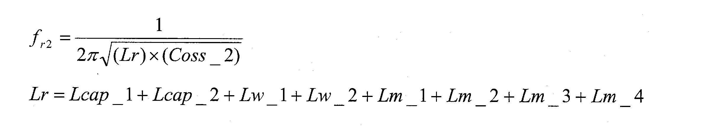
したがって、キャリア信号CrがU相制御指令信号Duよりも大きくなる時刻、すなわち、スイッチング素子Q11aがオンからオフ、スイッチング素子Q12aがオフからオンとなる時刻に発生するリンギング電圧の周波数frは数5のようになる。
Therefore, the time when the carrier signal Cr is larger than the U-phase control instruction signal Du, that is, the number is the frequency f r of the ringing voltage generated switching element Q11a from ON OFF, the time at which the switching element Q12a is turned from OFF 5 become that way.

数5より、周波数frはモータ104には影響されず、キャパシタ111とU相アーム112uとで決定される。電磁界シミュレーション等を用いてLm_1やLm_2等の各寄生インダクタンス成分を算出すれば、設計段階で数5より周波数frを求めることができる。また、周波数frが求まることにより数2の位相シフト量α[sec]も求まることとなる。よって、設計段階で所定の位相差αの値を設定することが可能である。
Than the number 5, the frequency f r is not affected by the motor 104 is determined by the capacitor 111 and the U-phase arm 112u. Be calculated each parasitic inductance components such Lm_1 and Lm_2 using an electromagnetic field simulation, etc., it is possible to obtain the frequency f r from the number 5 in the design phase. Further, when the frequency fr is obtained, the phase shift amount α [sec] of Equation 2 is also obtained. Therefore, it is possible to set the value of the predetermined phase difference α at the design stage.
なお、図4ではU相アーム112uのみに対する周波数frを算出したが、V相アーム112v、W相アーム112wがU相アーム112uと仕様が同一の部品で構成されているため、V相アーム112v、W相アーム112wにおけるスイッチング動作で発生するリンギング電圧の周波数frは、数5に示すものとなる。
Since was calculated frequency f r for only 4 in U-phase arm 112u, the V-phase arm 112v, W-phase arm 112w is the U-phase arm 112u and specifications are composed of the same components, V-phase arm 112v , the frequency f r of the ringing voltage generated by the switching operation in the W-phase arm 112w is as shown in Equation 5.
≪まとめ≫
本実施形態に係る電力変換装置の構成によれば、各スイッチング素子の端子間に発生するリンギング電圧が、各スイッチング素子間で互いに打ち消される。また、本実施形態では特許文献1とは異なり、各スイッチング素子から発生するスイッチングノイズを、その発生源である、スイッチング素子Q11a,Q11bとキャパシタ111とを結ぶ閉回路内で抑制することが可能である。図5は、本実施形態に係る効果を説明するための図である。図5では、図4と同様に、U相アーム112u,キャパシタ111のみを図示している。スイッチング素子Q11は、スイッチング素子Q11a,スイッチング素子Q11bを区別して図示しているが、スイッチング素子Q12は図4と同様に、簡略化したものを図示している。 ≪Summary≫
According to the configuration of the power conversion device according to the present embodiment, the ringing voltage generated between the terminals of the switching elements is canceled out between the switching elements. Also, in this embodiment, unlikePatent Document 1, switching noise generated from each switching element can be suppressed in a closed circuit connecting the switching elements Q11a and Q11b and the capacitor 111, which are the generation sources. is there. FIG. 5 is a diagram for explaining the effect according to the present embodiment. 5, only the U-phase arm 112u and the capacitor 111 are shown in the same manner as FIG. The switching element Q11 is illustrated by distinguishing between the switching element Q11a and the switching element Q11b, but the switching element Q12 is simplified as in FIG.
本実施形態に係る電力変換装置の構成によれば、各スイッチング素子の端子間に発生するリンギング電圧が、各スイッチング素子間で互いに打ち消される。また、本実施形態では特許文献1とは異なり、各スイッチング素子から発生するスイッチングノイズを、その発生源である、スイッチング素子Q11a,Q11bとキャパシタ111とを結ぶ閉回路内で抑制することが可能である。図5は、本実施形態に係る効果を説明するための図である。図5では、図4と同様に、U相アーム112u,キャパシタ111のみを図示している。スイッチング素子Q11は、スイッチング素子Q11a,スイッチング素子Q11bを区別して図示しているが、スイッチング素子Q12は図4と同様に、簡略化したものを図示している。 ≪Summary≫
According to the configuration of the power conversion device according to the present embodiment, the ringing voltage generated between the terminals of the switching elements is canceled out between the switching elements. Also, in this embodiment, unlike
上述したように、スイッチング素子Q11aとQ11bには仕様が同一のスイッチング素子が使用されているため、これらのスイッチング素子の出力容量(Coss_1)や、これらと他の構成要素等とを結ぶ配線のインダクタンス(Lm_1,Lm_2)は同一である。また、キャパシタ111とスイッチング素子Q11aとを結ぶ配線距離と、キャパシタ111とスイッチング素子Q11bとを結ぶ配線距離が同一であれば、これらの配線のインダクタンスはともにLw_1とおける。したがって、スイッチング素子Q11a,Q11bの端子間に発生するリンギング電圧Vra,Vrbの周波数frは同一となる。
As described above, since the switching elements having the same specifications are used for the switching elements Q11a and Q11b, the output capacitance (Coss_1) of these switching elements and the inductance of the wiring connecting these to other components, etc. (Lm_1, Lm_2) are the same. Further, if the wiring distance connecting capacitor 111 and switching element Q11a is the same as the wiring distance connecting capacitor 111 and switching element Q11b, the inductance of these wirings can be Lw_1. Therefore, the switching elements Q11a, ringing voltage Vra generated between Q11b of terminals, the frequency f r of the Vrb is the same.
図5に示すように、本実施形態においては、リンギング電圧Vra,Vrbを、スイッチング素子Q11a,Q11bとキャパシタ111とを結ぶ閉回路内で打ち消し合うことができ、図5のVrで示すように閉回路内における電圧変動が抑制される。したがって、電力変換装置内の寄生容量や配線等を経由し電源へと伝わる伝導ノイズはもちろんのこと、電力変換装置外の空間へ放射される放射ノイズに対する抑制効果も期待できる。また、スイッチングノイズを、発生源である上記閉回路内で抑制するので、いわゆるノーマルモードノイズとコモンモードノイズの両方に対して抑制効果を発揮することができる。
As shown in FIG. 5, in this embodiment, the ringing voltages Vra and Vrb can be canceled in a closed circuit connecting the switching elements Q11a and Q11b and the capacitor 111, and are closed as indicated by Vr in FIG. voltage variations in the circuit is suppressed. Therefore, not only the conduction noise transmitted to the power supply via the parasitic capacitance and wiring in the power converter, but also the effect of suppressing radiation noise radiated to the space outside the power converter can be expected. Further, since the switching noise is suppressed in the closed circuit that is a generation source, it is possible to exert an effect of suppressing both so-called normal mode noise and common mode noise.
また、本実施形態の手法によれば、三相インバータ102よりも負荷側(モータ104側)でリンギング電圧を打ち消し合う手法とは異なり、EMIフィルターやシールドなどの各種ノイズ抑制部品を使用することなく、スイッチングノイズの抑制効果が得られる。ノイズ抑制部品を使用する場合であっても、ノイズ抑制効果の小さな部品で済むので、負荷駆動システム100が大型化することがない。
Also, according to the method of the present embodiment, unlike the method of canceling the ringing voltage on the load side (motor 104 side) with respect to the three-phase inverter 102, various noise suppression components such as an EMI filter and a shield are not used. , suppression of switching noise can be obtained. Even when a noise suppression component is used, a component having a small noise suppression effect is sufficient, and the load drive system 100 does not increase in size.
[第1の実施形態の変形例]
第1の実施形態(図1)では、PWM信号生成部107で生成されたPWM信号を、位相シフト部108で位相シフトさせることにより、各スイッチング素子用のPWM信号を生成する構成であった。一方、本変形例では、各スイッチング素子用のキャリア信号を生成し、それらの信号を基に各スイッチング素子用のPWM信号を生成する構成である。以下、図6を参照しながら具体的に説明する。 [Modification of First Embodiment]
In the first embodiment (FIG. 1), the PWM signal generated by the PWMsignal generation unit 107 is phase-shifted by the phase shift unit 108 to generate the PWM signal for each switching element. On the other hand, in this modification, a carrier signal for each switching element is generated, and a PWM signal for each switching element is generated based on these signals. Hereinafter, this will be specifically described with reference to FIG.
第1の実施形態(図1)では、PWM信号生成部107で生成されたPWM信号を、位相シフト部108で位相シフトさせることにより、各スイッチング素子用のPWM信号を生成する構成であった。一方、本変形例では、各スイッチング素子用のキャリア信号を生成し、それらの信号を基に各スイッチング素子用のPWM信号を生成する構成である。以下、図6を参照しながら具体的に説明する。 [Modification of First Embodiment]
In the first embodiment (FIG. 1), the PWM signal generated by the PWM
図6は第1の実施形態の変形例に係る電力変換装置を備える負荷駆動システム100Aの全体構成を示す図である。図6に示す構成と第1の実施形態(図1)との異なる点は、電力変換装置113Aにおけるコントローラ105Aの構成、主にキャリア信号生成部106AとPWM信号生成部107Aである。以下、U相アーム112uのハイサイドスイッチング素子群Q11を中心に説明を続ける。
FIG. 6 is a diagram illustrating an overall configuration of a load drive system 100A including a power conversion device according to a modification of the first embodiment. The difference between the configuration shown in FIG. 6 and the first embodiment (FIG. 1) is the configuration of the controller 105A in the power conversion device 113A, mainly the carrier signal generation unit 106A and the PWM signal generation unit 107A. Hereinafter, the description will be continued focusing on the high-side switching element group Q11 of the U-phase arm 112u.
キャリア信号生成部106Aは、スイッチング素子Q11a,Q11b用のPWM信号Pua,Pubを生成するための鋸波のキャリア信号Cra,Crbを生成し、次段のPWM信号生成部107Aに出力する。
The carrier signal generation unit 106A generates sawtooth carrier signals Cra and Crb for generating the PWM signals Pua and Pub for the switching elements Q11a and Q11b, and outputs them to the PWM signal generation unit 107A in the next stage.
図7は、本変形例に係るキャリア信号生成部106Aの構成の一例を示す回路図である。
FIG. 7 is a circuit diagram showing an example of the configuration of the carrier signal generation unit 106A according to this modification.
パルス信号発生部は、一定周期で発生する幅の狭いパルス波形であるパルス信号Plを生成し、次段の位相シフト回路に出力する。
The pulse signal generation unit generates a pulse signal Pl that is a narrow pulse waveform generated at a constant period, and outputs the pulse signal Pl to the phase shift circuit at the next stage.
位相シフト回路は、入力されたパルス信号Plに基づき、各スイッチング素子用のパルス信号を生成する。位相シフト回路は、パルス信号Plを第3の位相角だけシフトさせてパルス信号Pl1を生成するとともに、パルス信号Plを第4の位相角だけシフトさせてパルス信号Pl2を生成する。第4の位相角は、第3の位相角に対してα[sec]だけ遅れている。パルス信号Pl1はトランジスタTr1に出力され、パルス信号Pl2はトランジスタTr2に出力される。
The phase shift circuit generates a pulse signal for each switching element based on the input pulse signal Pl. The phase shift circuit shifts the pulse signal Pl by the third phase angle to generate the pulse signal Pl1, and shifts the pulse signal Pl by the fourth phase angle to generate the pulse signal Pl2. The fourth phase angle is delayed by α [sec] with respect to the third phase angle. The pulse signal Pl1 is output to the transistor Tr1, and the pulse signal Pl2 is output to the transistor Tr2.
トランジスタTr1,Tr2は、パルス信号Pl1,Pl2が入力されることにより、一定の周期で一瞬の期間だけオンとなる。また、パルス信号Pl2はパルス信号Pl1に対し、α[sec]遅延しているので、それに従って、トランジスタTr2がオンとなるタイミングもトランジスタTr1に対しα[sec]遅延することとなる。
Transistors Tr1 and Tr2 are turned on for a moment in a constant cycle when pulse signals Pl1 and Pl2 are input. Further, since the pulse signal Pl2 is delayed by α [sec] relative to the pulse signal Pl1, the timing at which the transistor Tr2 is turned on is also delayed by α [sec] relative to the transistor Tr1.
トランジスタTr1(Tr2)がオフの期間では、キャパシタC3は定電流源Iへ向けて放電しており、キャパシタC3の電圧は一定速度で降下する。一方、トランジスタTr1(Tr2)がオンの期間では、キャパシタC3は充電を行っており、キャパシタC3の電圧は一定周期で瞬時に上昇する。その結果、所定時間をかけて第1レベルから第2レベルへ遷移したのち第2レベルから第1レベルへのリセットを繰り返し、かつ、互いに位相がα[sec]ずれた鋸波のキャリア信号Cra,Crbが生成される。
During the period when the transistor Tr1 (Tr2) is off, the capacitor C3 is discharged toward the constant current source I, and the voltage of the capacitor C3 drops at a constant speed. On the other hand, during the period in which the transistor Tr1 (Tr2) is on, the capacitor C3 is charged, and the voltage of the capacitor C3 increases instantaneously at a constant period. As a result, after transitioning from the first level to the second level over a predetermined time, the reset from the second level to the first level is repeated, and the sawtooth carrier signals Cra, Crb is generated.
また、図7で示した回路構成以外にも、例えば、特許文献2の図3に開示されているような回路構成によっても実施することが可能である。
Further, in addition to the circuit configuration shown in FIG. 7, for example, the circuit configuration disclosed in FIG. 3 of Patent Document 2 can be used.
PWM信号生成部107A(図6)は、キャリア信号CraとCrbに基づき、スイッチング素子Q11a用のPWM信号Puaおよびスイッチング素子Q11b用のPWM信号Pubを生成する。最終的にスイッチング素子Q11a,Q11bに出力されるPWM信号Pua,Pubは、第1の実施形態におけるPWM信号Pua,Pub(図3(b)、(c))と同一のものとなる。
PWM signal generation unit 107A (FIG. 6) generates PWM signal Pu for switching element Q11a and PWM signal Pub for switching element Q11b based on carrier signals Cra and Crb. The PWM signals Pua and Pub finally output to the switching elements Q11a and Q11b are the same as the PWM signals Pua and Pub (FIGS. 3B and 3C) in the first embodiment.
したがって、本変形例においても第1の実施形態と同様のノイズ抑制効果を得ることが可能である。
Therefore, also in this modification, it is possible to obtain the same noise suppression effect as in the first embodiment.
[第2の実施形態]
第1の実施形態においては、2個のスイッチング素子間でリンギング電圧を互いに打ち消されるようにする構成を示した。本実施形態では、3個のスイッチング素子間でリンギング電圧を互いに打ち消されるようにする構成について説明する。 [Second Embodiment]
In the first embodiment, the configuration has been described in which the ringing voltages are canceled out between the two switching elements. In the present embodiment, a configuration will be described in which the ringing voltages are canceled out between the three switching elements.
〈構成〉
図8は、第2の実施形態に係る電力変換装置の一部構成、特に三相インバータ202および位相シフト部208を示す図である。 <Constitution>
FIG. 8 is a diagram illustrating a partial configuration of the power conversion device according to the second embodiment, in particular, a three-phase inverter 202 and a phase shift unit 208.
図8は、第2の実施形態に係る電力変換装置の一部構成、特に三相インバータ202および位相シフト部208を示す図である。 <Constitution>
FIG. 8 is a diagram illustrating a partial configuration of the power conversion device according to the second embodiment, in particular, a three-
本実施形態に係る三相インバータ202は、第1の実施形態と同様に、U相アーム212u,V相アーム212v,W相アーム212wを構成するハイサイドスイッチング素子群Q21,Q23,Q25およびローサイドスイッチング素子群Q22,Q24,Q26のそれぞれにおいて、複数のスイッチング素子が並列接続されてなる。しかし、並列接続されているスイッチング素子の個数が第1の実施形態と異なる。
Similar to the first embodiment, the three-phase inverter 202 according to this embodiment includes a high-side switching element group Q21, Q23, Q25 and a low-side switching that constitute a U-phase arm 212u, a V-phase arm 212v, and a W-phase arm 212w. In each of the element groups Q22, Q24, Q26, a plurality of switching elements are connected in parallel. However, the number of switching elements connected in parallel is different from that of the first embodiment.
図8に示すように、U相アーム212uにおいて、ハイサイドスイッチング素子群Q21は、スイッチング素子Q21a,Q21b,Q21cの3個のスイッチング素子が並列接続されてなり、ローサイドスイッチング素子群Q22は、スイッチング素子Q22a,Q22b,Q22cの3個のスイッチング素子が並列接続されてなる。また、U相アーム212uと同様に、V相アーム212vのハイサイドスイッチング素子群Q23は、スイッチング素子Q23a,Q23b,Q23cの3個のスイッチング素子が、ローサイドスイッチング素子群Q24は、スイッチング素子Q24a,Q24b,Q24cの3個のスイッチング素子がそれぞれ並列接続されてなる。さらに、W相アーム212wにおいても同様に、ハイサイドスイッチング素子群Q25は、スイッチング素子Q25a,Q25b,Q25cの3個のスイッチング素子が、ローサイドスイッチング素子群Q26は、スイッチング素子Q26a,Q26b,Q26cの3個のスイッチング素子がそれぞれ並列接続されてなる。
As shown in FIG. 8, in the U-phase arm 212u, the high-side switching element group Q21 includes three switching elements Q21a, Q21b, and Q21c connected in parallel, and the low-side switching element group Q22 includes a switching element. Three switching elements Q22a, Q22b, and Q22c are connected in parallel. Similarly to the U-phase arm 212u, the high-side switching element group Q23 of the V-phase arm 212v has three switching elements Q23a, Q23b, and Q23c, and the low-side switching element group Q24 has switching elements Q24a and Q24b. , Q24c are connected in parallel. Similarly, in the W-phase arm 212w, the high-side switching element group Q25 includes three switching elements Q25a, Q25b, and Q25c, and the low-side switching element group Q26 includes three switching elements Q26a, Q26b, and Q26c. Each of the switching elements is connected in parallel.
なお、位相シフト部208は、第1の実施形態に係る位相シフト部108と略同様の構成であり、図8に特に図示していない構成も、第1の実施形態と略同様である。以下、U相アーム212uのハイサイドスイッチング素子群Q21を中心に説明する。
The phase shift unit 208 has substantially the same configuration as that of the phase shift unit 108 according to the first embodiment, and the configuration not particularly shown in FIG. 8 is also substantially the same as that of the first embodiment. Hereinafter, the description will focus on the high-side switching element group Q21 of the U-phase arm 212u.
位相シフト部208は、PWM信号生成部(図示せず)から入力されたPWM信号Puに基づき、スイッチング素子Q21a用のPWM信号Pua,スイッチング素子Q21b用のPWM信号Pub,スイッチング素子Q21c用のPWM信号Pucを生成し、次段のゲート駆動回路GDに出力する。位相シフト部208は、PWM信号Puを第1の位相角だけシフトさせてPWM信号Puaを生成し、PWM信号Puを第2の位相角だけシフトさせてPWM信号Pubを生成し、PWM信号Puを第3の位相角だけシフトさせてPWM信号Pucを生成する。第2の位相角は、第1の位相角に対してα[sec](第1の実施形態で説明したものと同一である。)だけ遅れており、第3の位相角は、第2の位相角に対してα[sec]だけ遅れている。
The phase shift unit 208 is based on the PWM signal Pu input from the PWM signal generation unit (not shown), the PWM signal Pua for the switching element Q21a, the PWM signal Pub for the switching element Q21b, and the PWM signal for the switching element Q21c. Puc is generated and output to the gate drive circuit GD at the next stage. The phase shift unit 208 shifts the PWM signal Pu by the first phase angle to generate the PWM signal Pua, shifts the PWM signal Pu by the second phase angle to generate the PWM signal Pub, and generates the PWM signal Pu. The PWM signal Puc is generated by shifting by the third phase angle. The second phase angle is delayed by α [sec] (same as described in the first embodiment) with respect to the first phase angle, and the third phase angle is equal to the second phase angle. It is delayed by α [sec] with respect to the phase angle.
このようにすることにより、スイッチング素子Q21a,Q21b,Q21cの間で、スイッチング動作のタイミングを互いにずらすことができる。
By doing so, the timing of the switching operation can be shifted between the switching elements Q21a, Q21b, and Q21c.
〈スイッチングノイズ抑制原理〉
図9を用いて本実施形態におけるスイッチングノイズ抑制原理について説明する。図9は第2の実施形態に係るタイミングチャートを示す図である。ここではU相アーム212uのハイサイドスイッチング素子群Q21のみを取り上げて説明する。 <Switching noise suppression principle>
The switching noise suppression principle in this embodiment will be described with reference to FIG. FIG. 9 is a diagram illustrating a timing chart according to the second embodiment. Here, only the high-side switching element group Q21 of theU-phase arm 212u will be described.
図9を用いて本実施形態におけるスイッチングノイズ抑制原理について説明する。図9は第2の実施形態に係るタイミングチャートを示す図である。ここではU相アーム212uのハイサイドスイッチング素子群Q21のみを取り上げて説明する。 <Switching noise suppression principle>
The switching noise suppression principle in this embodiment will be described with reference to FIG. FIG. 9 is a diagram illustrating a timing chart according to the second embodiment. Here, only the high-side switching element group Q21 of the
図9(a)は、本実施形態に係るPWM信号生成部に入力される鋸波のキャリア信号CrとU相制御指令信号Duの電圧波形を示す図であり、これらの電圧波形は第1の実施形態に係るもの(図3(a))と同様である。
FIG. 9A is a diagram illustrating voltage waveforms of the sawtooth carrier signal Cr and the U-phase control command signal Du input to the PWM signal generation unit according to the present embodiment. These voltage waveforms are the first waveform. This is the same as that according to the embodiment (FIG. 3A).
図9(b)は位相シフト部208から出力されるPWM信号Puaの電圧波形を、図9(c)はPWM信号Pubの電圧波形を、図9(d)はPWM信号Pucの電圧波形をそれぞれ示している。図9(b),(c),(d)に示すように、PWM信号PucはPWM信号Puaに対し2α[sec](αは第1の実施形態で説明したものと同一である。)、PWM信号Pubに対しα[sec]遅延している。
9B shows the voltage waveform of the PWM signal Pua output from the phase shift unit 208, FIG. 9C shows the voltage waveform of the PWM signal Pub, and FIG. 9D shows the voltage waveform of the PWM signal Puc. Show. As shown in FIGS. 9B, 9C, and 9D, the PWM signal Puc is 2α [sec] with respect to the PWM signal Pua (α is the same as that described in the first embodiment). It is delayed by α [sec] with respect to the PWM signal Pub.
図9(e)は、スイッチング素子Q21aの端子間の電圧変動を、図9(f)はスイッチング素子Q21bの端子間の電圧変動を、図9(g)は、スイッチング素子Q21cの端子間の電圧変動を、図9(h)は図9(e),(f),(g)に示す(B)付近の拡大図をそれぞれ示している。
FIG. 9E shows the voltage fluctuation between the terminals of the switching element Q21a, FIG. 9F shows the voltage fluctuation between the terminals of the switching element Q21b, and FIG. 9G shows the voltage between the terminals of the switching element Q21c. FIG. 9 (h) shows an enlarged view around (B) shown in FIGS. 9 (e), (f), and (g).
以下、第1の実施形態と同様に、U相制御指令信号Duよりもキャリア信号Crが大きくなった場合にオンからオフへの状態遷移が起こるものとして説明する。
Hereinafter, as in the first embodiment, it is assumed that the state transition from on to off occurs when the carrier signal Cr becomes larger than the U-phase control command signal Du.
先ず、図9の時刻(1)について説明する。図9(a)において、キャリア信号CrとU相制御指令信号Duが交差し、図9(b)に示すPWM信号Puaはオンからオフへ状態遷移する。この状態遷移に伴い、スイッチング素子Q21aはオンからオフへ切り換わり、スイッチング素子Q21aの端子間電圧はハイレベルからローレベルへ遷移する(図9(e))。このとき、スイッチング素子Q21aの端子間にはリンギング電圧Vraが発生する。
First, time (1) in FIG. 9 will be described. In FIG. 9A, the carrier signal Cr and the U-phase control command signal Du cross each other, and the PWM signal Pua shown in FIG. 9B transitions from on to off. With this state transition, the switching element Q21a is switched from on to off, and the voltage between the terminals of the switching element Q21a transitions from the high level to the low level (FIG. 9 (e)). At this time, a ringing voltage Vra is generated between the terminals of the switching element Q21a.
次に、図9の時刻(2)について説明する。図9(c)に示すPWM信号Pubは、時刻(1)からα[sec]遅延して、オンからオフへ状態遷移する。この状態遷移に伴い、スイッチング素子Q21bはオンからオフへ切り換わり、スイッチング素子Q21bの端子間電圧はハイレベルからローレベルへ遷移する(図9(f))。このとき、スイッチング素子Q21bの端子間にはリンギング電圧Vrbが発生する。
Next, a description will be given time in FIG. 9 (2). The PWM signal Pub shown in FIG. 9C transitions from on to off with a delay of α [sec] from time (1). With this state transition, the switching element Q21b is switched from on to off, and the voltage between the terminals of the switching element Q21b transitions from a high level to a low level (FIG. 9 (f)). At this time, a ringing voltage Vrb is generated between the terminals of the switching element Q21b.
そうすると、図9(h)に示すように、リンギング電圧Vraとリンギング電圧Vrbは、互いに位相が反転した関係となる。このようにすることで、スイッチング素子Q21a,Q21bが行うオンからオフへのスイッチング動作に伴って発生するリンギング電圧Vra,Vrbは互いに打ち消され、その結果、これらのスイッチング素子から発生するスイッチングノイズが抑制される。
Then, as shown in FIG. 9 (h), the ringing voltage Vra and the ringing voltage Vrb have a relationship in which the phases are inverted. By doing so, the ringing voltages Vra and Vrb generated by the switching operation from on to off performed by the switching elements Q21a and Q21b cancel each other, and as a result, switching noise generated from these switching elements is suppressed. Is done.
次に、図9の時刻(3)について説明する。図9(d)に示すPWM信号Pucは、時刻(2)からα[sec]、時刻(1)から2α[sec]遅延してオンからオフへ状態遷移する。この状態遷移に伴い、スイッチング素子Q21cはオンからオフへ切り換わり、スイッチング素子Q21cの端子間電圧はハイレベルからローレベルへ遷移する(図9(g))。このとき、スイッチング素子Q21cの端子間にはリンギング電圧Vrcが発生する。このリンギング電圧Vrcは他のリンギング電圧と互いに打ち消されることなくそのまま残ることとなる。
Next, time (3) in FIG. 9 will be described. The PWM signal Puc shown in FIG. 9D transitions from on to off with a delay of α [sec] from time (2) and 2α [sec] from time (1). With this state transition, the switching element Q21c is switched from on to off, and the voltage between the terminals of the switching element Q21c transitions from the high level to the low level (FIG. 9 (g)). At this time, a ringing voltage Vrc is generated between the terminals of the switching element Q21c. This ringing voltage Vrc remains as it is without canceling out other ringing voltages.
続いて、時刻(4)について説明する。図9(a)において、キャリア信号CrとU相制御指令信号Duが交差し、図9(b)に示すPWM信号Puaはオフからオンへ状態遷移する。この状態遷移に伴い、スイッチング素子Q21aはオフからオンへ切り換わり、スイッチング素子Q21aの端子間電圧はローレベルからハイレベルへ遷移する(図9(e))。このときも時刻(1)と同様に、スイッチング素子Q21aの端子間にリンギング電圧Vraが発生する。
Next, the time (4) will be described. In FIG. 9A, the carrier signal Cr and the U-phase control command signal Du intersect, and the PWM signal Pua shown in FIG. 9B transitions from OFF to ON. With this state transition, the switching element Q21a is switched from OFF to ON, and the voltage between the terminals of the switching element Q21a transitions from the low level to the high level ((e) in FIG. 9). At this time, similarly to the time (1), the ringing voltage Vra is generated between the terminals of the switching element Q21a.
次に、時刻(5)において、図9(c)に示すPWM信号Pubは、時刻(4)からα[sec]遅延して、オフからオンへ状態遷移する。この状態遷移に伴い、スイッチング素子Q21bはオフからオンへ切り換わり、スイッチング素子Q21bの端子間電圧はローレベルからハイレベルへ遷移する(図9(f))。このときも時刻(2)と同様に、スイッチング素子Q21bの端子間にリンギング電圧Vrbが発生する。
Next, at time (5), the PWM signal Pub shown in FIG. 9 (c) transitions from OFF to ON with a delay of α [sec] from time (4). With this state transition, the switching element Q21b is switched from off to on, and the voltage across the terminals of the switching element Q21b transitions from low level to high level (FIG. 9 (f)). At this time, similarly to time (2), the ringing voltage Vrb is generated between the terminals of the switching element Q21b.
次に、図9の時刻(6)について説明する。図9(d)に示すPWM信号Pucは、時刻(5)からα[sec]、時刻(4)から2α[sec]遅延してオフからオンへ状態遷移する。この状態遷移に伴い、スイッチング素子Q21cはオフからオンへ切り換わり、スイッチング素子Q21cの端子間電圧はローレベルからハイレベルへ遷移する(図9(g))。このときも時刻(3)と同様に、スイッチング素子Q21cの端子間にリンギング電圧Vrcが発生する。このリンギング電圧Vrcは他のリンギング電圧と互いに打ち消されることなくそのまま残ることとなる。
Next, time (6) in FIG. 9 will be described. The PWM signal Puc shown in FIG. 9D transitions from OFF to ON with a delay of α [sec] from time (5) and 2α [sec] from time (4). With this state transition, the switching element Q21c is switched from OFF to ON, and the voltage between the terminals of the switching element Q21c transitions from low level to high level (FIG. 9 (g)). At this time, similarly to the time (3), the ringing voltage Vrc is generated between the terminals of the switching element Q21c. This ringing voltage Vrc remains as it is without canceling out other ringing voltages.
以上説明したように、上記の構成によれば、リンギング電圧Vra,Vrbについては、スイッチング素子がオンからオフへの状態遷移に伴って発生する場合、ならびに、オフからオンへの状態遷移に伴って発生する場合の両方を打ち消すようにすることが可能である。一方、リンギング電圧Vrcは打ち消されずに残ってしまうため、第1の実施形態と比較するとスイッチングノイズ抑制効果は劣る。しかしながら、従来のように3個のスイッチング素子が同期して動作させる場合と比較すると、スイッチングノイズは3分の1程度に抑制することが可能である。
As described above, according to the above configuration, the ringing voltages Vra and Vrb are generated when the switching element is generated along with the state transition from on to off, and with the state transition from off to on. It is possible to cancel both of the occurrences. On the other hand, since the ringing voltage Vrc remains without being canceled, the switching noise suppression effect is inferior to that of the first embodiment. However, the switching noise can be suppressed to about one third as compared with the conventional case where three switching elements are operated in synchronization.
[第2の実施形態の変形例]
本変形例では、第2の実施形態と同様に3個のスイッチング素子間でリンギング電圧が互いに打ち消されるようにする構成であるが、各スイッチング素子で発生するリンギング電圧が理想的な正弦波である場合に、特に良好なノイズ抑制効果を奏する構成について説明する。 [Modification of Second Embodiment]
In this modification, the ringing voltage is canceled between the three switching elements as in the second embodiment, but the ringing voltage generated in each switching element is an ideal sine wave. In this case, a configuration that exhibits a particularly good noise suppression effect will be described.
本変形例の構成は第2の実施形態(図8)と同様である。本変形例に係る位相シフト部は、第2の実施形態に係る位相シフト部208と同様に、PWM信号Pua,Pub,Pucを生成するが、第2の実施形態にあっては所定の位相差がα[sec]であったのに対し、本変形例ではこの所定の位相差はβ[sec]である。βはスイッチング素子に発生するリンギング電圧の周波数frを用いて数6で定義される。
The configuration of this modification is the same as that of the second embodiment (FIG. 8). Similar to the phase shift unit 208 according to the second embodiment, the phase shift unit according to the present modification generates the PWM signals Pua, Pub, and Puc. In the second embodiment, a predetermined phase difference is generated. Is α [sec], in the present modification, this predetermined phase difference is β [sec]. β is defined by the number 6 using the frequency f r of the ringing voltage generated in the switching element.

数6から分かるように、位相差βはリンギング電圧の3分の1周期分に相当する。図10を用いて、本変形例における具体的なスイッチングノイズ抑制原理について説明する。
As can be seen from Equation 6, the phase difference β corresponds to one-third period of the ringing voltage. A specific switching noise suppression principle in the present modification will be described with reference to FIG.
図10は本変形例に係るタイミングチャートを示す図であり、図10(a),(b),(c)は、それぞれ、スイッチング素子Q21a,Q21b,Q21cに発生するリンギング電圧Vra,Vrb,Vrcの波形の拡大図である。位相差βをリンギング電圧の3分の1周期分に相当する値に設定することにより、リンギング電圧Vra,Vrb,Vrcが正確な正弦波である場合には、これらのリンギング電圧の足し合わせはゼロとなり、リンギング電圧が互いに相殺される。
FIG. 10 is a diagram illustrating a timing chart according to the present modification. FIGS. 10A, 10B, and 10C illustrate ringing voltages Vra, Vrb, and Vrc generated in the switching elements Q21a, Q21b, and Q21c, respectively. it is an enlarged view of the waveform. By setting the phase difference β to a value corresponding to one-third period of the ringing voltage, when the ringing voltages Vra, Vrb, and Vrc are accurate sine waves, the sum of these ringing voltages is zero. And the ringing voltages cancel each other.
実際上は、リンギング電圧Vra,Vrb,Vrcは正確な正弦波とならないため、リンギング電圧の足し合わせはゼロとはならないものの、効率の良いスイッチングノイズ抑制効果が期待できる。
Actually, since the ringing voltages Vra, Vrb, and Vrc do not become accurate sine waves, the sum of the ringing voltages does not become zero, but an efficient switching noise suppression effect can be expected.
[第3の実施形態]
第1の実施形態では、スイッチング素子を2個並列に接続することで定格電流を倍増させた三相インバータにおいて、並列関係にあるスイッチング素子のスイッチングのタイミングをずらすことで、これらのスイッチング素子から発生するリンギング電圧を打ち消すようにする構成を説明した。第3の実施形態では、U相アームを構成するスイッチング素子,V相アームを構成するスイッチング素子,W相アームを構成するスイッチング素子のスイッチングのタイミングをずらすことで、U相アーム,V相アーム,W相アーム間でリンギング電圧を打ち消すようにする構成を説明する。 [Third Embodiment]
In the first embodiment, in a three-phase inverter in which the rated current is doubled by connecting two switching elements in parallel, the switching timing of the switching elements in parallel relation is shifted to generate from these switching elements. The configuration for canceling the ringing voltage is explained. In the third embodiment, by switching the switching timing of the switching elements constituting the U-phase arm, the switching elements constituting the V-phase arm, and the switching elements constituting the W-phase arm, the U-phase arm, the V-phase arm, A configuration for canceling the ringing voltage between the W-phase arms will be described.
〈構成〉
図11は、第3の実施形態に係る電力変換装置を備える負荷駆動システム300の全体構成を示す図である。 <Constitution>
FIG. 11 is a diagram illustrating an overall configuration of aload driving system 300 including the power conversion device according to the third embodiment.
図11は、第3の実施形態に係る電力変換装置を備える負荷駆動システム300の全体構成を示す図である。 <Constitution>
FIG. 11 is a diagram illustrating an overall configuration of a
負荷駆動システム300は、直流電源DC,電力変換装置313,モータ304を備える。直流電源DC、モータ304は、それぞれ、第1の実施形態における直流電源DC,モータ104と同一の構成であるが、電力変換装置313は第1の実施形態における電力変換装置113と構成が異なる。
The load driving system 300 includes a DC power source DC, a power conversion device 313, and a motor 304. The direct-current power source DC and the motor 304 have the same configuration as the direct-current power source DC and the motor 104 in the first embodiment, respectively, but the configuration of the power conversion device 313 is different from that of the power conversion device 113 in the first embodiment.
電力変換装置313は、電圧検出部301,電流検出部303,三相インバータ302,コントローラ305からなる。電圧検出部301,電流検出部303はそれぞれ、第1の実施形態における電圧検出部101,電流検出部103と同一の構成である。一方、三相インバータ302,コントローラ305は、第1の実施形態における三相インバータ102,コントローラ105と構成が異なる。
The power conversion device 313 includes a voltage detection unit 301, a current detection unit 303, a three-phase inverter 302, and a controller 305. The voltage detection unit 301 and the current detection unit 303 have the same configuration as the voltage detection unit 101 and the current detection unit 103 in the first embodiment, respectively. On the other hand, the three-phase inverter 302 and the controller 305 are different in configuration from the three-phase inverter 102 and the controller 105 in the first embodiment.
三相インバータ302は、U相アーム312u,V相アーム312v,W相アーム312wを備え、U相アーム312uは、さらに、直列接続されたハイサイドスイッチング素子Q31とローサイドスイッチング素子Q32から構成される。第1の実施形態とは異なり、本実施形態のハイサイドスイッチング素子Q31およびローサイドスイッチング素子Q32は、それぞれ単一のスイッチング素子から構成されている。
The three-phase inverter 302 includes a U-phase arm 312u, a V-phase arm 312v, and a W-phase arm 312w. The U-phase arm 312u further includes a high-side switching element Q31 and a low-side switching element Q32 connected in series. Unlike the first embodiment, the high-side switching element Q31 and the low-side switching element Q32 of this embodiment are each composed of a single switching element.
V相アーム312vとW相アーム312wは、U相アーム312uと同様の構成である。また、スイッチング素子Q31~Q36は、共通のスイッチング素子により構成されている。
The V-phase arm 312v and the W-phase arm 312w have the same configuration as the U-phase arm 312u. The switching elements Q31 to Q36 are constituted by a common switching element.
本実施形態の電力変換装置313においては、U相アーム312u,V相アーム312v,W相アーム312wのうちいずれか1つとキャパシタ311とを含む閉回路が、アーム毎に形成されている。すなわち、ある一の閉回路には、U相アーム312uとキャパシタ311とが含まれており、このような閉回路が電力変換装置313にはアームの個数分(3個)形成されている。以下、ハイサイドスイッチング素子Q31,Q33,Q35を中心に説明する。
In the power conversion device 313 of this embodiment, a closed circuit including any one of the U-phase arm 312u, the V-phase arm 312v, and the W-phase arm 312w and the capacitor 311 is formed for each arm. That is, one closed circuit includes a U-phase arm 312u and a capacitor 311. Such a closed circuit is formed in the power conversion device 313 by the number of arms (three). Hereinafter, the description will focus on the high-side switching elements Q31, Q33, and Q35.
コントローラ305は、キャリア信号生成部306,PWM信号生成部307,位相シフト部308,電流指令部309,電流制御部310から構成される。キャリア信号生成部306,PWM信号生成部307,電流指令部309,電流制御部310は、それぞれ、第1の実施形態におけるキャリア信号生成部106,PWM信号生成部107,電流指令部109,電流制御部110と同一の構成である。一方、位相シフト部308は、第1の実施形態における位相シフト部108と構成が異なる。
The controller 305 includes a carrier signal generation unit 306, a PWM signal generation unit 307, a phase shift unit 308, a current command unit 309, and a current control unit 310. The carrier signal generation unit 306, the PWM signal generation unit 307, the current command unit 309, and the current control unit 310 are the carrier signal generation unit 106, the PWM signal generation unit 107, the current command unit 109, and the current control, respectively, in the first embodiment. parts 110 have the same configuration as. On the other hand, the phase shift unit 308 is different in configuration from the phase shift unit 108 in the first embodiment.
位相シフト部308は、入力されたPWM信号Pu,Pv,Pwに基づきハイサイドスイッチング素子Q31に出力されるPWM信号Pu’,ハイサイドスイッチング素子Q33に出力されるPWM信号Pv’,ハイサイドスイッチング素子Q35に出力されるPWM信号Pw’を生成し、次段のゲート駆動回路GDに出力する。位相シフト部308は、PWM信号Puを第1の位相角だけシフトさせてPWM信号Pu’を生成し、PWM信号Pvを第2の位相角だけシフトさせてPWM信号Pv’を生成し、PWM信号Pwを第3の位相角だけシフトさせてPWM信号Pw’を生成する。第2の位相角は、第1の位相角に対してα[sec](第1の実施形態で説明したものと同一である。)だけ遅れており、第3の位相角は、第2の位相角に対してα[sec]だけ遅れている。
The phase shift unit 308 includes a PWM signal Pu ′ output to the high side switching element Q31 based on the input PWM signals Pu, Pv, and Pw, a PWM signal Pv ′ output to the high side switching element Q33, and the high side switching element. The PWM signal Pw ′ output to Q35 is generated and output to the next stage gate drive circuit GD. The phase shift unit 308 shifts the PWM signal Pu by the first phase angle to generate the PWM signal Pu ′, shifts the PWM signal Pv by the second phase angle to generate the PWM signal Pv ′, and generates the PWM signal. The PWM signal Pw ′ is generated by shifting Pw by the third phase angle. The second phase angle is delayed by α [sec] (same as described in the first embodiment) with respect to the first phase angle, and the third phase angle is equal to the second phase angle. It is delayed by α [sec] with respect to the phase angle.
このようにすることにより、ハイサイドスイッチング素子Q31,Q33,Q35との間で、スイッチング動作のタイミングを互いにずらすことが可能となる。
This makes it possible to shift the timing of the switching operation between the high-side switching elements Q31, Q33, and Q35.
ここで、U相アーム312uのスイッチング素子Q31のスイッチング動作により、U相アーム312uとキャパシタ311を含む閉回路に発生するリンギング電圧の周波数は、当該閉回路に含まれるインダクタンスとその閉回路に含まれるアームを構成するスイッチング素子Q31の出力容量とで規定される。また、図4において、スイッチング素子Q11,Q12を、それぞれ本実施形態におけるスイッチング素子Q31,Q32と置き換えると、図4は、U相アーム312uとキャパシタ311を含む閉回路を示していることになる。したがって、図4において説明した周波数frの算出方法を本実施形態においても適用することができる。
Here, the frequency of the ringing voltage generated in the closed circuit including the U-phase arm 312u and the capacitor 311 by the switching operation of the switching element Q31 of the U-phase arm 312u is included in the inductance included in the closed circuit and the closed circuit. It is defined by the output capacity of the switching element Q31 constituting the arm. In FIG. 4, when switching elements Q11 and Q12 are replaced with switching elements Q31 and Q32 in the present embodiment, respectively, FIG. 4 shows a closed circuit including U-phase arm 312u and capacitor 311. Therefore, the method for calculating the frequency fr described in FIG. 4 can also be applied to this embodiment.
U相アーム312uとキャパシタ311を含む閉回路においては、スイッチング素子Q31に含まれる配線のインダクタンスがLm_1,Lm_2に、キャパシタ311に含まれるインダクタンスがLcap_1,Lcap_2に、スイッチング素子Q31とキャパシタ311を接続する配線のインダクタンスがLm_3,Lm_4,Lw_1、Lw_2に、それぞれ相当する。したがって、この閉回路に含まれるインダクタンスは、Lcap_1,Lcap_2,Lw_1、Lw_2,Lm_1,Lm_2,Lm_3,Lm_4とからなることになる。
In a closed circuit including the U-phase arm 312u and the capacitor 311, the switching element Q31 and the capacitor 311 are connected to the inductance of the wiring included in the switching element Q31 with Lm_1 and Lm_2, and the inductance included in the capacitor 311 with Lcap_1 and Lcap_2. The wiring inductances correspond to Lm_3, Lm_4, Lw_1, and Lw_2, respectively. Therefore, the inductance included in this closed circuit is composed of Lcap_1, Lcap_2, Lw_1, Lw_2, Lm_1, Lm_2, Lm_3, and Lm_4.
〈スイッチングノイズ抑制原理〉
図12に示すタイミングチャート図を用いて、本実施形態におけるスイッチングノイズ抑制原理について説明する。 <Switching noise suppression principle>
The switching noise suppression principle in this embodiment will be described with reference to the timing chart shown in FIG.
図12に示すタイミングチャート図を用いて、本実施形態におけるスイッチングノイズ抑制原理について説明する。 <Switching noise suppression principle>
The switching noise suppression principle in this embodiment will be described with reference to the timing chart shown in FIG.
図12(a)は、PWM信号生成部307に入力される鋸波のキャリア信号Cr、U相制御指令信号Du、V相制御指令信号Dv、W相制御指令信号Dwの電圧波形を示す図である。キャリア信号Crは、第1の実施形態の場合と同様の鋸波波形である。U相制御指令信号Du、V相制御指令信号Dv、W相制御指令信号Dwは位相が各々120°、電気角で2π/3ラジアンずれている。
12A is a diagram illustrating voltage waveforms of the sawtooth carrier signal Cr, the U-phase control command signal Du, the V-phase control command signal Dv, and the W-phase control command signal Dw input to the PWM signal generation unit 307. FIG. is there. The carrier signal Cr has a sawtooth waveform similar to that in the first embodiment. The U-phase control command signal Du, V-phase control command signal Dv, and W-phase control command signal Dw are 120 ° out of phase and 2π / 3 radians at an electrical angle.
図12(b)は、位相シフト部308から出力されるPWM信号Pu’の電圧波形を示している。
FIG. 12B shows a voltage waveform of the PWM signal Pu ′ output from the phase shift unit 308.
図12(c)は、位相シフト部308に入力されるPWM信号Pvの電圧波形(点線)と、位相シフト部308から出力されるPWM信号Pv’(実線)をそれぞれ示している。PWM信号Pv’はPWM信号Pvに対し、α[sec]遅延している。
FIG. 12C shows the voltage waveform (dotted line) of the PWM signal Pv input to the phase shift unit 308 and the PWM signal Pv ′ (solid line) output from the phase shift unit 308, respectively. The PWM signal Pv ′ is delayed by α [sec] with respect to the PWM signal Pv.
図12(d)は、位相シフト部308に入力されるPWM信号Pwの電圧波形(点線)と、位相シフト部308から出力されるPWM信号Pw’(実線)をそれぞれ示している。PWM信号Pw’はPWM信号Pwに対し、2α[sec]遅延している。
FIG. 12D shows the voltage waveform (dotted line) of the PWM signal Pw input to the phase shift unit 308 and the PWM signal Pw ′ (solid line) output from the phase shift unit 308, respectively. The PWM signal Pw ′ is delayed by 2α [sec] with respect to the PWM signal Pw.
図12(e)は、ハイサイドスイッチング素子Q31の端子間の電圧変動を、図12(f)はハイサイドスイッチング素子Q33の端子間の電圧変動を、図12(g)は、ハイサイドスイッチング素子Q35の端子間の電圧変動を、図12(h)は図12(e),(f)、(g)に示す(C)付近の拡大図をそれぞれ示している。
12 (e) shows the voltage fluctuation between the terminals of the high-side switching element Q31, FIG. 12 (f) shows the voltage fluctuation between the terminals of the high-side switching element Q33, and FIG. 12 (g) shows the high-side switching element. FIG. 12 (h) shows an enlarged view of the vicinity of (C) shown in FIGS. 12 (e), 12 (f), and 12 (g).
以下、制御指令信号Du、Dv、Dwよりもキャリア信号Crが大きくなった場合にオンからオフへの状態遷移が起こるものとして説明する。
Hereinafter, description will be made assuming that the state transition from on to off occurs when the carrier signal Cr becomes larger than the control command signals Du, Dv, and Dw.
先ず、図12の時刻(1)について説明する。図12(a)において、キャリア信号CrとU相制御指令信号Duが交差し、図12(b)に示すPWM信号Pu’はオンからオフへ状態遷移する。この状態遷移に伴い、ハイサイドスイッチング素子Q31はオンからオフへ切り換わり、ハイサイドスイッチング素子Q31の端子間電圧はハイレベルからローレベルへ遷移する(図12(e))。このとき、ハイサイドスイッチング素子Q31の端子間にはリンギング電圧Vruが発生する。
First, the time (1) in FIG. 12 will be described. In FIG. 12A, the carrier signal Cr and the U-phase control command signal Du cross each other, and the PWM signal Pu ′ shown in FIG. 12B transitions from on to off. With this state transition, the high-side switching element Q31 is switched from on to off, and the voltage between the terminals of the high-side switching element Q31 transitions from the high level to the low level (FIG. 12 (e)). At this time, a ringing voltage Vru is generated between the terminals of the high-side switching element Q31.
ここで、本実施形態のようにキャリア信号として鋸波を用いている場合、時刻(1)においては、制御指令信号Dv,Dwもキャリア信号Crと交差するため、PWM信号生成部307から出力されるPWM信号Pv,Pwにおいてもオンからオフへの状態遷移が起こる。仮に、このPWM信号Pv,Pwを位相シフト部308で位相シフトさせずにハイサイドスイッチング素子Q33,Q35のゲート端子に出力した場合には、ハイサイドスイッチング素子Q31,Q33,Q35で同時にスイッチング動作が行われてしまうことになる。そうすると、ハイサイドスイッチング素子Q31,Q33,Q35からは、互いに同位相のリンギング電圧が発生してしまうこととなるため、スイッチングノイズが三重に重畳してしまう。そこで、本実施形態においては、同時にスイッチング動作が行われることがないよう、PWM信号Pv,Pwの位相を位相シフト部308でずらす構成としている。
Here, when the sawtooth wave is used as the carrier signal as in the present embodiment, the control command signals Dv and Dw also intersect with the carrier signal Cr at time (1), and thus are output from the PWM signal generation unit 307. Also in the PWM signals Pv and Pw, the state transition from on to off occurs. If the PWM signals Pv and Pw are output to the gate terminals of the high-side switching elements Q33 and Q35 without being phase-shifted by the phase shift unit 308, the high-side switching elements Q31, Q33, and Q35 are simultaneously switched. Will be done. As a result, ringing voltages having the same phase are generated from the high-side switching elements Q31, Q33, and Q35, so that switching noise is superimposed in triplicate. Therefore, in this embodiment, the phase shift unit 308 is configured to shift the phases of the PWM signals Pv and Pw so that the switching operation is not performed at the same time.
次に、図12の時刻(2)について説明する。上述した理由により、位相シフト部308から出力されるPWM信号Pv’は、PWM信号Pvに対してα[sec]の位相差が設けられている(図12(c))。ここでのαは第1の実施形態における数2で定義される。本実施形態では、数2における周波数frはハイサイドスイッチング素子Q31に発生するリンギング電圧Vruの周波数としている。なお、前述したように、スイッチング素子Q31~Q36は、耐圧や電流容量などの仕様が同一のスイッチング素子により構成されているため、各スイッチング素子に発生するリンギング電圧の周波数は同値である。
Next, time (2) in FIG. 12 will be described. For the reasons described above, the PWM signal Pv ′ output from the phase shift unit 308 has a phase difference of α [sec] with respect to the PWM signal Pv (FIG. 12C). Here, α is defined by Equation 2 in the first embodiment. In the present embodiment, the frequency f r in equation 2 is the frequency of the ringing voltage Vru occurring high-side switching element Q31. As described above, since the switching elements Q31 to Q36 are composed of switching elements having the same specifications such as withstand voltage and current capacity, the frequency of the ringing voltage generated in each switching element is the same value.
図12の時刻(2)において、図12(c)に示すPWM信号Pv’は、時刻(1)からα[sec]遅延して、オンからオフへ状態遷移する。この状態遷移に伴い、ハイサイドスイッチング素子Q33はオンからオフへ切り換わり、ハイサイドスイッチング素子Q33の端子間電圧はハイレベルからローレベルへ遷移する(図12(f))。このとき、ハイサイドスイッチング素子Q33の端子間にはリンギング電圧Vrvが発生する。
At time (2) in FIG. 12, the PWM signal Pv ′ shown in FIG. 12 (c) is changed from on to off with a delay of α [sec] from time (1). With this state transition, the high-side switching element Q33 is switched from on to off, and the voltage between the terminals of the high-side switching element Q33 transitions from the high level to the low level (FIG. 12 (f)). At this time, a ringing voltage Vrv is generated between the terminals of the high-side switching element Q33.
そうすると、図12(h)に示すように、リンギング電圧Vruとリンギング電圧Vrvは、互いに位相が反転した関係となる。このようにすることで、ハイサイドスイッチング素子Q31,Q33が行うオンからオフへのスイッチング動作に伴って発生するリンギング電圧Vru,Vrvは互いに打ち消され、その結果、これらのスイッチング素子から発生するスイッチングノイズが抑制される。
Then, as shown in FIG. 12 (h), the ringing voltage Vru and the ringing voltage Vrv have a relationship in which the phases are inverted. By doing so, the ringing voltages Vru and Vrv generated in association with the switching operation from on to off performed by the high-side switching elements Q31 and Q33 are canceled out, and as a result, switching noise generated from these switching elements. Is suppressed.
次に、図12の時刻(3)について説明する。V相と同様の理由により、図12(d)に示すPWM信号Pw’は、時刻(1)から2α[sec]遅延して、オンからオフへ状態遷移する。この状態遷移に伴い、ハイサイドスイッチング素子Q35はオンからオフへ切り換わり、ハイサイドスイッチング素子Q35の端子間電圧はハイレベルからローレベルへ遷移する(図12(g))。このとき、ハイサイドスイッチング素子Q35の端子間にはリンギング電圧Vrwが発生する。このリンギング電圧Vrwは他のリンギング電圧と互いに打ち消されることなくそのまま残ることとなる。
Next, time (3) in FIG. 12 will be described. For the same reason as the V phase, the PWM signal Pw ′ shown in FIG. 12 (d) is shifted from on to off with a delay of 2α [sec] from time (1). With this state transition, the high-side switching element Q35 is switched from on to off, and the voltage between the terminals of the high-side switching element Q35 transitions from the high level to the low level (FIG. 12 (g)). At this time, a ringing voltage Vrw is generated between the terminals of the high-side switching element Q35. This ringing voltage Vrw remains as it is without canceling out other ringing voltages.
以上説明したように、上記の構成によれば、スイッチング素子がオンからオフへの状態遷移に伴って発生する場合において、リンギング電圧Vru,Vrvを互いに打ち消すようにすることが可能である。一方、リンギング電圧Vrwは打ち消されずに残ってしまうため、第1の実施形態と比較するとスイッチングノイズ抑制効果は劣る。しかしながら、図12(b)~(d)の点線で示すように、U相,V相,W相のスイッチング素子全てが同時にスイッチング動作させる場合と比較すると、スイッチングノイズは3分の1程度に抑制することが可能である。
As described above, according to the above configuration, the ringing voltages Vru and Vrv can be canceled with each other when the switching element is generated with the state transition from on to off. On the other hand, since the ringing voltage Vrw remains without being canceled, the switching noise suppression effect is inferior compared with the first embodiment. However, as shown by the dotted lines in FIGS. 12B to 12D, the switching noise is suppressed to about one third as compared with the case where all the switching elements of the U phase, the V phase, and the W phase are simultaneously switched. Is possible.
また、本実施形態のように、U相,V相,W相のスイッチング素子間でリンギング電圧を互いに打ち消し合うようにするには、キャリア信号としては、例えば、鋸波のように、所定時間をかけて第1レベルから第2レベルへ遷移したのち第2レベルから第1レベルへのリセットを繰り返すようなキャリア信号を用いることが好ましい。このようなキャリア信号を用いた場合、キャリア信号がリセットされる時刻(図12の時刻(1))においては、U相,V相,W相のPWM信号全てでオンからオフ(もしくはオフからオン)の状態遷移が起こる。その結果、U相,V相,W相のスイッチング素子で同時にスイッチング動作が行われてしまい、スイッチングノイズ増大につながることとなる。
In addition, in order to cancel the ringing voltages between the switching elements of the U phase, the V phase, and the W phase as in the present embodiment, the carrier signal is set to a predetermined time, such as a sawtooth wave, for example. It is preferable to use a carrier signal that repeats reset from the second level to the first level after transition from the first level to the second level. When such a carrier signal is used, at the time when the carrier signal is reset (time (1) in FIG. 12), all the U-phase, V-phase, and W-phase PWM signals are turned from on to off (or from off to on). ) State transition occurs. As a result, U-phase, V-phase, will be switching operation is performed simultaneously with the switching elements of the W-phase, and thus lead to switching noise increases.
上述したように、同時にスイッチング動作が行われる時刻はキャリア信号がリセットされるタイミングに対応して周期的に起こるものであり、かつ、デューティ比によって変動しない。本実施形態では、この同時にスイッチング動作が行われるタイミングがデューティ比によって変動しない点に着目し、この時刻を位相シフトの基準として利用することにより、各相のスイッチング素子におけるスイッチング動作のタイミングを制御することが可能となっている。
As described above, the time at which the switching operation is performed simultaneously occurs periodically corresponding to the timing at which the carrier signal is reset, and does not vary with the duty ratio. In this embodiment, paying attention to the fact that the timing at which the switching operation is simultaneously performed does not vary depending on the duty ratio, the timing of the switching operation in the switching element of each phase is controlled by using this time as a phase shift reference. It is possible.
なお、第1の実施形態においては、スイッチング素子がオンからオフへの状態遷移に伴って発生するリンギング電圧、ならびに、オフからオンへの状態遷移に伴って発生するリンギング電圧の両者を打ち消すようにすることが可能であった。しかしながら、本実施形態では、打ち消すことができるリンギング電圧はどちらか一方に限られる。なぜなら、図12(b)~(d)に示すように、キャリア信号が所定時間をかけて第1レベルから第2レベルへ遷移している期間においては、キャリア信号と制御指令信号が交差するタイミングはデューティ比によって変動するからである。そのため、キャリア信号と制御指令信号が交差するタイミングを位相シフトの基準として利用することは困難である。しかしながら、どちらか一方のリンギング電圧は打ち消すことができるので、各相用のPWM信号を位相シフトさせない場合と比較してノイズレベルは約半分に抑制することができる。
In the first embodiment, the switching element cancels both the ringing voltage generated in accordance with the state transition from on to off and the ringing voltage generated in accordance with the state transition from off to on. It was possible to do. However, in this embodiment, the ringing voltage that can be canceled is limited to either one. This is because, as shown in FIGS. 12B to 12D, the timing at which the carrier signal and the control command signal intersect in the period in which the carrier signal transitions from the first level to the second level over a predetermined time. This is because it varies depending on the duty ratio. Therefore, it is difficult to use the timing at which the carrier signal and the control command signal intersect as the phase shift reference. However, since either one of the ringing voltages can be canceled out, the noise level can be suppressed to about half compared to the case where the PWM signal for each phase is not phase-shifted.
なお、第1の実施形態の変形例(図6)のように、あらかじめ各相間で所定の位相差を設けた各相用のキャリア信号を生成しておき、それらのキャリア信号を基に各相用のPWM信号を生成する構成をとることも可能である。
As in the modification of the first embodiment (FIG. 6), a carrier signal for each phase in which a predetermined phase difference is provided between the phases is generated in advance, and each phase is based on the carrier signals. It is also possible to adopt a configuration for generating a PWM signal for use.
≪スイッチングノイズ抑制原理の検証≫
本実施形態に係るスイッチングノイズ抑制原理の検証結果を、図13乃至図15を用いて説明する。 ≪Verification of switching noise suppression principle≫
The verification result of the switching noise suppression principle according to the present embodiment will be described with reference to FIGS.
本実施形態に係るスイッチングノイズ抑制原理の検証結果を、図13乃至図15を用いて説明する。 ≪Verification of switching noise suppression principle≫
The verification result of the switching noise suppression principle according to the present embodiment will be described with reference to FIGS.
本実施形態に係るスイッチングノイズ抑制原理の検証は、具体的には図13に示す回路を用いて行った。図13に示す原理検証用の回路は図11に示す回路構成を基本としており、図11におけるものと同一の構成には同じ符号を付している。
The verification of the switching noise suppression principle according to the present embodiment was specifically performed using the circuit shown in FIG. The principle verification circuit shown in FIG. 13 is based on the circuit configuration shown in FIG. 11, and the same components as those shown in FIG.
先ず、パルスジェネレータ321からハイサイドスイッチング素子Q31、Q33のゲート端子へパルス信号が送られる。このパルス信号が入力されることにより、ハイサイドスイッチング素子Q31,Q33においてスイッチング動作が行われる。ここで、パルスジェネレータ321から出力されるパルス信号は、ハイサイドスイッチング素子Q31とQ33間で時間差が設けられており、これによってスイッチング動作のタイミングがずれることとなる。
First, a pulse signal is sent from the pulse generator 321 to the gate terminals of the high-side switching elements Q31 and Q33. By inputting this pulse signal, the high-side switching elements Q31 and Q33 perform a switching operation. Here, the pulse signal output from the pulse generator 321 has a time difference between the high-side switching elements Q31 and Q33, and the timing of the switching operation is thereby shifted.
次に、ハイサイドスイッチング素子Q31,Q33をスイッチング動作させた状態での、ローサイドスイッチング素子のQ32,Q34の端子間電圧を、それぞれU相電圧検出部322u,V相電圧検出部322vで観測した。なお、U相アームとV相アームには負荷320が接続されている。
Next, the voltage between the terminals of the low-side switching elements Q32 and Q34 in the state where the high-side switching elements Q31 and Q33 are switched is observed by the U-phase voltage detection unit 322u and the V-phase voltage detection unit 322v, respectively. A load 320 is connected to the U-phase arm and the V-phase arm.
電圧検出部322u,322vで観測したローサイドスイッチング素子のQ32,Q34の端子間電圧変動を図14に示す。図14(a)は本実施形態のスイッチング動作を想定した場合の結果であり、図14(b)は比較例における結果である。また、各図において、ローサイドスイッチング素子Q32の端子間電圧変動を実線で、ローサイドスイッチング素子Q34の端子間電圧変動を点線でそれぞれ示している。
Voltage detection unit 322U, the voltage variation across Q32, Q34 of the terminals of the low side switching element as observed by 322v shown in FIG 14. 14 (a) is a result of assuming the switching operation of the present embodiment, FIG. 14 (b) is a result of a comparative example. Moreover, in each figure, the voltage fluctuation between the terminals of the low side switching element Q32 is indicated by a solid line, and the voltage fluctuation between the terminals of the low side switching element Q34 is indicated by a dotted line.
本実施形態を想定した図14(a)においては、ハイサイドスイッチング素子Q31,Q33に入力されるパルス信号の時間差を上記のα[sec]としており、リンギング電圧の位相が互いに反転するようにしている。一方、比較例の図14(b)においては、入力されるパルス信号の時間差は略ゼロであり、リンギング電圧の位相は略同じである。
In FIG. 14A assuming this embodiment, the time difference between the pulse signals input to the high-side switching elements Q31 and Q33 is α [sec], and the phase of the ringing voltage is inverted with respect to each other. Yes. On the other hand, in FIG. 14B of the comparative example, the time difference between the input pulse signals is substantially zero, and the phase of the ringing voltage is substantially the same.
続いて、直流電源DCと三相インバータとの間に、擬似電源回路網(LISN)318(図13)を接続し、ローサイドスイッチング素子Q32,Q34の端子間に図14に示すような電圧変動が起こっている状態で、スペクトラムアナライザ319によりノイズスペクトラムを計測し、その結果を図15に示した。図15の実線が本実施形態における結果(図14(a)に対応する。)、点線が比較例における結果(図14(b)に対応する。)である。
Subsequently, a pseudo power supply network (LISN) 318 (FIG. 13) is connected between the DC power supply DC and the three-phase inverter, and voltage fluctuations as shown in FIG. 14 occur between the terminals of the low-side switching elements Q32 and Q34. In the state of occurrence, the noise spectrum was measured by the spectrum analyzer 319, and the result is shown in FIG. The solid line in FIG. 15 is the result in the present embodiment (corresponding to FIG. 14A), and the dotted line is the result in the comparative example (corresponding to FIG. 14B).
図15に示すように、比較例では、60[MHz],65[MHz]の周波数帯域に、大きなノイズレベルのピーク値が観測されている。一方、本実施の形態では、60[MHz]で約4dB、65[MHz]で約10dB程度、ノイズを抑制することが可能であることが分かった。図14(a)の細部に注目すると、50nsecの期間はリンギング電圧の約3周期分に相当し、このことより、リンギング電圧の1周期は約16.7nsecであることが分かる。そして、この16.7nsecの逆数をとると約60[MHz]となり、これはすなわち、図15においてノイズ抑制効果が顕著に表れた周波数帯域と一致する。
As shown in FIG. 15, in the comparative example, a large noise level peak value is observed in the frequency bands of 60 [MHz] and 65 [MHz]. On the other hand, in the present embodiment, it has been found that noise can be suppressed by about 4 dB at 60 [MHz] and about 10 dB at 65 [MHz]. When attention is paid to the details of FIG. 14A, the period of 50 nsec corresponds to about three periods of the ringing voltage, and from this, it can be seen that one period of the ringing voltage is about 16.7 nsec. Then, when the reciprocal of 16.7 nsec is taken, it becomes about 60 [MHz], which corresponds to the frequency band in which the noise suppression effect is remarkably exhibited in FIG.
以上のことより、リンギング電圧が打ち消されるようにしたことによって、三相インバータから直流電源DCへ伝導するノイズが抑制されたことが示された。
From the above, it was shown that noise conducted from the three-phase inverter to the DC power source DC was suppressed by canceling the ringing voltage.
本実施形態においては、リンギング電圧の打ち消し合いがなされるスイッチング素子は、互いに異なる相のスイッチング素子である。よって、これらのスイッチング素子に入力されるPWM信号は、位相の異なる制御指令信号に基づき生成されるものである。一方、第1、第2の実施形態およびその変形例においては、リンギング電圧の打ち消し合いがなされるスイッチング素子は、同一相におけるスイッチング素子である。よって、これらのスイッチング素子に入力されるPWM信号は、同じ制御指令信号に基づき生成されるものである。したがって、第1,第2の実施形態およびその変形例の場合のように、同一相におけるスイッチング素子同士でリンギング電圧の打ち消し合いがなされる実施形態の方が、より精度の良いノイズ抑制を図ることが可能である。
In this embodiment, the switching elements with which the ringing voltages are canceled are switching elements of different phases. Therefore, the PWM signals input to these switching elements are generated based on control command signals having different phases. On the other hand, in the first and second embodiments and the modifications thereof, the switching elements that cancel out the ringing voltages are switching elements in the same phase. Therefore, the PWM signal input to these switching elements is generated based on the same control command signal. Therefore, as in the case of the first and second embodiments and the modifications thereof, the embodiment in which the ringing voltages are canceled out between the switching elements in the same phase achieves more accurate noise suppression. Is possible.
[第3の実施形態の変形例]
本変形例では、第3の実施形態と同様にU相,V相,W相のスイッチング素子間でリンギング電圧が互いに打ち消されるようにする構成であるが、各スイッチング素子で発生するリンギング電圧が理想的な正弦波である場合に、特に良好なノイズ抑制効果を奏する構成について説明する。 [Modification of Third Embodiment]
In this modification, the ringing voltage is canceled between U-phase, V-phase, and W-phase switching elements as in the third embodiment, but the ringing voltage generated in each switching element is ideal. In the case of a typical sine wave, a configuration that exhibits a particularly good noise suppression effect will be described.
本変形例の構成は第3の実施形態(図11)と同様である。本変形例に係る位相シフト部は、第3の実施形態に係る位相シフト部308と同様に、PWM信号Pu’,Pv’,Pw’を生成するが、第3の実施形態にあっては所定の位相差がα[sec]であったのに対し、本変形例ではこの所定の位相差はβ[sec]である。このβは第2の実施形態の変形例と同様に、スイッチング素子に発生するリンギング電圧の周波数frを用いて数6で定義される。本変形例では、数6における周波数frはハイサイドスイッチング素子Q31に発生するリンギング電圧Vruの周波数である。
The configuration of this modification is the same as that of the third embodiment (FIG. 11). Similar to the phase shift unit 308 according to the third embodiment, the phase shift unit according to the present modification generates the PWM signals Pu ′, Pv ′, and Pw ′. In the third embodiment, the phase shift unit is predetermined. The predetermined phase difference is β [sec] in the present modification. The β is defined by the number 6 using the frequency f r of the ringing voltage in the same manner as in the modification of the second embodiment, generated in the switching element. In this modification, the frequency f r in equation 6 is the frequency of the ringing voltage Vru occurring high-side switching element Q31.
第2の実施形態の変形例と同様に、この位相差βはリンギング電圧の3分の1周期分に相当する。次に、図16を用いて、本変形例における具体的なスイッチングノイズ抑制原理について説明する。
As in the modification of the second embodiment, this phase difference β corresponds to one-third period of the ringing voltage. Next, a specific switching noise suppression principle in the present modification will be described with reference to FIG.
図16は本変形例に係るタイミングチャートを示す図であり、図16(a),(b),(c)は、それぞれ、ハイサイドスイッチング素子Q31,Q33,Q35に発生するリンギング電圧Vru,Vrv,Vrwの波形の拡大図である。位相差βをリンギング電圧の3分の1周期分に相当する値に設定することにより、リンギング電圧Vru,Vrv,Vrwが正確な正弦波である場合には、これらのリンギング電圧の足し合わせはゼロとなり、リンギング電圧が互いに相殺される。
FIG. 16 is a diagram illustrating a timing chart according to the present modification. FIGS. 16A, 16B, and 16C are ringing voltages Vru and Vrv generated in the high-side switching elements Q31, Q33, and Q35, respectively. , Vrw waveform enlarged view. By setting the phase difference β to a value corresponding to one third of the ringing voltage, when the ringing voltages Vru, Vrv, and Vrw are accurate sine waves, the sum of these ringing voltages is zero. And the ringing voltages cancel each other.
実際上は、リンギング電圧Vru,Vrv,Vrwは正確な正弦波とならないため、リンギング電圧の足し合わせはゼロとはならないものの、効率の良いスイッチングノイズ抑制効果が期待できる。
Actually, since the ringing voltages Vru, Vrv, and Vrw do not become accurate sine waves, the sum of the ringing voltages does not become zero, but an efficient switching noise suppression effect can be expected.
[第4の実施形態]
図17は、第4の実施形態に係る電力変換装置を備える負荷駆動システム400の全体構成を示す図である。図17を用いて第4の実施形態について説明する。 [Fourth Embodiment]
FIG. 17 is a diagram illustrating an overall configuration of aload driving system 400 including a power conversion device according to the fourth embodiment. A fourth embodiment will be described with reference to FIG.
図17は、第4の実施形態に係る電力変換装置を備える負荷駆動システム400の全体構成を示す図である。図17を用いて第4の実施形態について説明する。 [Fourth Embodiment]
FIG. 17 is a diagram illustrating an overall configuration of a
負荷駆動システム400は、直流電源DC,電力変換装置413,モータ404を備える。直流電源DC,モータ404は、それぞれ、第3の実施形態(図11)における直流電源DC,モータ304と同一の構成であるが、電力変換装置413は第3の実施形態における電力変換装置313と構成が異なる。
The load drive system 400 includes a DC power source DC, a power conversion device 413, and a motor 404. The DC power source DC and the motor 404 have the same configuration as the DC power source DC and the motor 304 in the third embodiment (FIG. 11), respectively, but the power conversion device 413 is the same as the power conversion device 313 in the third embodiment. The configuration is different.
電力変換装置413は、電圧検出部401,電流検出部403,三相インバータ402,コントローラ405からなる。電流検出部403,三相インバータ402は、それぞれ、第3の実施形態における電流検出部303,三相インバータ302と同一の構成である。一方、電圧検出部401,コントローラ405は、第3の実施形態における電圧検出部301,コントローラ305と構成が異なる。
The power converter 413 includes a voltage detection unit 401, a current detection unit 403, a three-phase inverter 402, and a controller 405. Current detecting unit 403, a three-phase inverter 402, respectively, the current detecting unit 303 in the third embodiment, the same structure as the three-phase inverter 302. On the other hand, the voltage detection unit 401 and the controller 405 are different in configuration from the voltage detection unit 301 and the controller 305 in the third embodiment.
コントローラ405は、キャリア信号生成部406,PWM信号生成部407,位相シフト部408,電流指令部409,電流制御部410から構成される。キャリア信号生成部406,PWM信号生成部407,電流指令部409,電流制御部410は、それぞれ、第3の実施形態におけるキャリア信号生成部306,PWM信号生成部307,電流指令部309,電流制御部310と同一の構成である。一方、位相シフト部408は、第3の実施形態における位相シフト部308と構成が異なる。
The controller 405 includes a carrier signal generation unit 406, a PWM signal generation unit 407, a phase shift unit 408, a current command unit 409, and a current control unit 410. The carrier signal generation unit 406, the PWM signal generation unit 407, the current command unit 409, and the current control unit 410 are respectively the carrier signal generation unit 306, the PWM signal generation unit 307, the current command unit 309, and the current control in the third embodiment. The configuration is the same as that of the unit 310. On the other hand, the phase shift unit 408 is different in configuration from the phase shift unit 308 in the third embodiment.
したがって、本実施形態に係る負荷駆動システム400と第3の実施形態との違いは、電圧検出部401で検出した直流電源DCの電圧値を位相シフト部408への入力として追加した点である。
Therefore, the difference between the load driving system 400 according to the present embodiment and the third embodiment is that the voltage value of the DC power source DC detected by the voltage detection unit 401 is added as an input to the phase shift unit 408.
リンギング電圧の周波数は、数1より、スイッチング素子の出力容量Cによって定まるが、スイッチング素子の端子間の電圧が高くなると、スイッチング素子の出力容量は小さくなる特性をもっていることが知られている。よって、リンギング電圧に基づくノイズが三相インバータ402から直流電源DC側へ伝導することにより電源電圧値が上がるにしたがって、リンギング電圧の周波数は大きくなる。そのため、電源電圧が大きく変動するシステムにおいて良好なノイズ抑制効果を得るためには、位相シフト部における位相差の設定値を可変にする必要がある。
The frequency of the ringing voltage is determined by the output capacity C of the switching element from Equation 1, but it is known that the output capacity of the switching element decreases as the voltage between the terminals of the switching element increases. Therefore, the frequency of the ringing voltage increases as the power supply voltage value increases as noise based on the ringing voltage is conducted from the three-phase inverter 402 to the DC power supply DC side. Therefore, in order to obtain a good noise suppression effect in a system in which the power supply voltage varies greatly, it is necessary to make the set value of the phase difference in the phase shift unit variable.
そこで、本実施形態では、電圧検出部401で検出した電源電圧値にしたがって、位相シフト部408において設ける位相差の設定値を可変とする。これは、電圧検出部401で検出した電源電圧値に対応する位相差の設定値を、あらかじめデータベースとして用意しておく等の方法により実施することが可能である。
Therefore, in the present embodiment, the set value of the phase difference provided in the phase shift unit 408 is made variable according to the power supply voltage value detected by the voltage detection unit 401. This can be performed by a method in which a set value of a phase difference corresponding to the power supply voltage value detected by the voltage detection unit 401 is prepared as a database in advance.
具体的には、各電源電圧値におけるスイッチング素子の出力容量が分かれば、数5によりリンギング電圧の周波数を算出することができる。そして、この周波数に基づき数2または数6から位相差の設定値を算出することによって、データベースを作成することができる。位相シフト部408は、電圧検出部401で検出した電源電圧値に基づくフィードバック信号を得て、当該信号に応じた位相差の設定値をデータベースから読み込み、位相シフト動作を行う。
Specifically, if the output capacitance of the switching elements in each of the power supply voltage value is known, it is possible to calculate the frequency of the ringing voltage by the number 5. Then, the database can be created by calculating the set value of the phase difference from Equation 2 or Equation 6 based on this frequency. The phase shift unit 408 obtains a feedback signal based on the power supply voltage value detected by the voltage detection unit 401, reads a set value of a phase difference corresponding to the signal from the database, and performs a phase shift operation.
以上説明したように、本実施形態によれば電源電圧値が大きく変動するシステムにおいても、効率的なノイズ抑制効果を得ることができる。
As described above, even in a system in which the power supply voltage value fluctuates greatly according to the present embodiment, it is possible to obtain an efficient noise suppression effect.
[第5の実施形態]
図18は、第5の実施形態に係る電力変換装置を備える負荷駆動システム500の全体構成を示す図である。図18を用いて第5の実施形態について説明する。 [Fifth Embodiment]
FIG. 18 is a diagram illustrating an overall configuration of aload driving system 500 including a power conversion device according to the fifth embodiment. The fifth embodiment will be described with reference to FIG.
図18は、第5の実施形態に係る電力変換装置を備える負荷駆動システム500の全体構成を示す図である。図18を用いて第5の実施形態について説明する。 [Fifth Embodiment]
FIG. 18 is a diagram illustrating an overall configuration of a
負荷駆動システム500は、直流電源DC,電力変換装置513,モータ504を備える。直流電源DC,モータ504は、それぞれ、第4の実施形態(図17)における直流電源DC,モータ404と同一の構成であるが、電力変換装置513は第4の実施形態における電力変換装置413と構成が異なる。
The load drive system 500 includes a DC power source DC, a power converter 513, and a motor 504. The direct current power source DC and the motor 504 have the same configuration as the direct current power source DC and the motor 404 in the fourth embodiment (FIG. 17), respectively, but the power conversion device 513 is the same as the power conversion device 413 in the fourth embodiment. The configuration is different.
電力変換装置513は、電流検出部501,503、三相インバータ502、コントローラ505からなる。電流検出部503,三相インバータ502は、それぞれ、第4の実施形態における電流検出部403,三相インバータ402と同一の構成である。一方、コントローラ505は、第4の実施形態におけるコントローラ405と構成が異なり、電流検出部501は第4の実施形態にはない構成である。
The power converter 513 includes current detectors 501 and 503, a three-phase inverter 502, and a controller 505. The current detection unit 503 and the three-phase inverter 502 have the same configuration as the current detection unit 403 and the three-phase inverter 402 in the fourth embodiment, respectively. On the other hand, the controller 505 has a different configuration from the controller 405 in the fourth embodiment, and the current detection unit 501 has a configuration that does not exist in the fourth embodiment.
コントローラ505は、キャリア信号生成部506,PWM信号生成部507,位相シフト部508,電流指令部509,電流制御部510から構成される。キャリア信号生成部506,PWM信号生成部507,電流指令部509,電流制御部510は、それぞれ、第4の実施形態におけるキャリア信号生成部406,PWM信号生成部407,電流指令部409,電流制御部410と同一の構成である。一方、位相シフト部508は、第4の実施形態における位相シフト部408と構成が異なる。
The controller 505 includes a carrier signal generation unit 506, a PWM signal generation unit 507, a phase shift unit 508, a current command unit 509, and a current control unit 510. The carrier signal generation unit 506, the PWM signal generation unit 507, the current command unit 509, and the current control unit 510 are respectively the carrier signal generation unit 406, the PWM signal generation unit 407, the current command unit 409, and the current control in the fourth embodiment. The configuration is the same as that of the unit 410. On the other hand, the phase shift unit 508 is different in configuration from the phase shift unit 408 in the fourth embodiment.
したがって、本実施形態に係る負荷駆動システム500と第4の実施形態との違いは、電流検出部501で検出した直流電源DCの電流値を位相シフト部508への入力とした点である。
Therefore, the difference between the load driving system 500 according to the present embodiment and the fourth embodiment is that the current value of the DC power source DC detected by the current detection unit 501 is input to the phase shift unit 508.
電流検出部501はハイパスフィルターを備えており、三相インバータ502から直流電源DC側へ伝導するリンギング電圧成分を検出する。リンギング電圧成分のゼロクロスを判定することでリンギング電圧の周波数を算出し、このリンギング電圧の周波数に基づき、数2または数6から位相差の設定値を決定する。位相シフト部508は、このように決定した位相差に基づき、位相シフト動作を行う。
Current detecting section 501 is provided with a high-pass filter, for detecting a ringing voltage component that conducts to the DC power supply DC side from the three-phase inverter 502. The frequency of the ringing voltage is calculated by determining the zero crossing of the ringing voltage component, and the set value of the phase difference is determined from Equation 2 or Equation 6 based on the frequency of the ringing voltage. The phase shift unit 508 performs a phase shift operation based on the phase difference determined in this way.
以上説明したように、本実施形態によればリンギング電圧の周波数帯域が変動するシステムにおいても、効率的なノイズ抑制効果を得ることができる。
As described above, according to the present embodiment, an efficient noise suppression effect can be obtained even in a system in which the frequency band of the ringing voltage varies.
[第6の実施形態]
図19は、第6の実施形態に係る電力変換装置を備える負荷駆動システム600の全体構成を示す図である。図19を用いて第6の実施形態について説明する。 [Sixth Embodiment]
FIG. 19 is a diagram illustrating an overall configuration of aload driving system 600 including the power conversion device according to the sixth embodiment. The sixth embodiment will be described with reference to FIG.
図19は、第6の実施形態に係る電力変換装置を備える負荷駆動システム600の全体構成を示す図である。図19を用いて第6の実施形態について説明する。 [Sixth Embodiment]
FIG. 19 is a diagram illustrating an overall configuration of a
負荷駆動システム600は、直流電源DC,電力変換装置613,モータ604を備える。直流電源DC,モータ604は、それぞれ、第5の実施形態(図18)における直流電源DC,モータ504と同一の構成であるが、電力変換装置613は第5の実施形態における電力変換装置513と構成が異なる。
The load drive system 600 includes a DC power source DC, a power conversion device 613, and a motor 604. The direct current power source DC and the motor 604 have the same configuration as the direct current power source DC and the motor 504 in the fifth embodiment (FIG. 18), respectively, but the power conversion device 613 is the same as the power conversion device 513 in the fifth embodiment. The configuration is different.
電力変換装置613は、電圧検出部601,電流検出部603,三相インバータ602,コントローラ605からなる。電圧検出部601,三相インバータ602は、それぞれ、第3の実施形態における電流検出部301、第5の実施形態における三相インバータ502と同一の構成である。一方、電流検出部603,コントローラ605は、第5の実施形態における電流検出部503,コントローラ505と構成が異なる。
The power converter 613 includes a voltage detection unit 601, a current detection unit 603, a three-phase inverter 602, and a controller 605. The voltage detection unit 601 and the three-phase inverter 602 have the same configuration as the current detection unit 301 in the third embodiment and the three-phase inverter 502 in the fifth embodiment, respectively. On the other hand, the current detection unit 603 and the controller 605 are different in configuration from the current detection unit 503 and the controller 505 in the fifth embodiment.
コントローラ605は、キャリア信号生成部606,PWM信号生成部607,位相シフト部608,電流指令部609,電流制御部610から構成される。キャリア信号生成部606,PWM信号生成部607,電流指令部609,電流制御部610は、それぞれ、第5の実施形態におけるキャリア信号生成部506,PWM信号生成部507,電流指令部509,電流制御部510と同一の構成である。一方、位相シフト部608は、第5の実施形態における位相シフト部508と構成が異なる。
The controller 605 includes a carrier signal generation unit 606, a PWM signal generation unit 607, a phase shift unit 608, a current command unit 609, and a current control unit 610. The carrier signal generation unit 606, the PWM signal generation unit 607, the current command unit 609, and the current control unit 610 are respectively the carrier signal generation unit 506, the PWM signal generation unit 507, the current command unit 509, and the current control in the fifth embodiment. The configuration is the same as that of the unit 510. On the other hand, the phase shift unit 608 is different in configuration from the phase shift unit 508 in the fifth embodiment.
したがって、第5の実施形態では直流電源DCの電流、すなわち、三相インバータ502の入力電流値を位相シフト部508への入力とする例を説明したが、本実施形態では、三相インバータ602の出力電流値を位相シフト部608への入力する点が異なる。
Therefore, in the fifth embodiment, an example in which the current of the DC power source DC, that is, the input current value of the three-phase inverter 502 is input to the phase shift unit 508 has been described. In the present embodiment, the three-phase inverter 602 The difference is that the output current value is input to the phase shift unit 608.
電流検出部603はハイパスフィルターを備えており、三相インバータ602からモータ604側へ伝導するリンギング電圧成分を検出する。リンギング電圧成分のゼロクロスを判定することでリンギング電圧の周波数を算出し、このリンギング電圧の周波数に基づき、数2または数6から位相差の設定値を決定する。位相シフト部608は、このように決定した位相差に基づき、位相シフト動作を行う。
Current detecting section 603 is provided with a high-pass filter, for detecting a ringing voltage component conducted from the three-phase inverter 602 to the motor 604 side. The frequency of the ringing voltage is calculated by determining the zero crossing of the ringing voltage component, and the set value of the phase difference is determined from Equation 2 or Equation 6 based on the frequency of the ringing voltage. The phase shift unit 608 performs a phase shift operation based on the phase difference determined in this way.
本実施形態によれば、第5の実施形態と同様に、リンギング電圧の周波数帯域が変動するシステムにおいても、効率的なノイズ抑制効果を得ることができる。さらに、本実施形態では、三相インバータ602の出力側の電流値を検出する構成であるので、第5の実施形態とは異なり、U相,V相,W相毎に出力電流値を検出することが可能である。したがって、本実施形態は、リンギング電圧の周波数がU相,V相,W相で異なるような場合に効果的であると言える。
According to the present embodiment, as in the fifth embodiment, an efficient noise suppression effect can be obtained even in a system in which the frequency band of the ringing voltage varies. Furthermore, in the present embodiment, since the current value on the output side of the three-phase inverter 602 is detected, unlike the fifth embodiment, the output current value is detected for each of the U phase, the V phase, and the W phase. It is possible. The present embodiments are, therefore, the frequency of the ringing voltage can be said to be effective when the U-phase, V-phase, W-phase at different like.
[第7の実施形態]
第1~第6の実施形態においては、三相インバータを構成する各スイッチング素子の電流流通率を変えて出力電圧を制御するPWM方式による説明をしたが、本発明はこれに限られない。本実施形態では、直流電源と三相インバータとの間にチョッパ回路を接続し、チョッパ回路の出力電圧を可変することでモータの入力電圧を可変制御する駆動方式、いわゆるPAM(Pulse Amplitude Modulation)方式による電力変換装置についての実施例を説明する。 [Seventh Embodiment]
In the first to sixth embodiments, the PWM method for controlling the output voltage by changing the current flow rate of each switching element constituting the three-phase inverter has been described, but the present invention is not limited to this. In the present embodiment, a drive system in which a chopper circuit is connected between a DC power supply and a three-phase inverter, and the input voltage of the motor is variably controlled by varying the output voltage of the chopper circuit, so-called PAM (Pulse Amplitude Modulation) system. An embodiment of the power conversion device according to will be described.
図20は本実施形態に係る電力変換装置を備える負荷駆動システム700の全体構成を示す図である。
FIG. 20 is a diagram illustrating an overall configuration of a load driving system 700 including the power conversion device according to the present embodiment.
負荷駆動システム700は直流電源DC,電力変換装置713,モータ704からなる。
The load drive system 700 includes a DC power source DC, a power conversion device 713, and a motor 704.
直流電源DCは電源系統を整流して得られる直流電源、または、バッテリタイプの直流電源である。
DC power source DC is a DC power source obtained by rectifying a power system or a battery type DC power source.
電力変換装置713は、昇圧チョッパ回路716,三相インバータ702,コントローラ705からなり、直流電源DCから供給される電力をU相,V相,W相の三相交流電力に変換し、モータ704に給電する。
The power conversion device 713 includes a step-up chopper circuit 716, a three-phase inverter 702, and a controller 705. The power conversion device 713 converts the power supplied from the DC power source DC into U-phase, V-phase, and W-phase three-phase AC power. Supply power.
昇圧チョッパ回路716は直流電源DCの電圧を昇圧し、昇圧後の直流電圧を三相インバータ702に出力する回路である。昇圧チョッパ回路716は、インダクタ714,ダイオード715,スイッチング素子群Q7,キャパシタ711を備える一般的な構成である。スイッチング素子群Q7は、第1および第2の実施形態のスイッチング素子群と同様に、スイッチング素子群Q7に流せる電流量を増加させることを目的として、スイッチング素子Q7a,Q7bが並列接続して構成されている。スイッチング素子Q7a,Q7bのゲート端子にはゲート駆動回路GDが接続されている。
The step-up chopper circuit 716 boosts the voltage of the DC power source DC and outputs the boosted DC voltage to the three-phase inverter 702. The step-up chopper circuit 716 has a general configuration including an inductor 714, a diode 715, a switching element group Q7, and a capacitor 711. The switching element group Q7 is configured by connecting switching elements Q7a and Q7b in parallel for the purpose of increasing the amount of current that can be passed through the switching element group Q7, similarly to the switching element groups of the first and second embodiments. ing. A gate drive circuit GD is connected to the gate terminals of the switching elements Q7a and Q7b.
三相インバータ702は、昇圧チョッパ回路716から出力される電力を三相交流電力に変換し、これをモータ704に給電する。三相インバータ702の詳細な構成は図示していないが、第3の実施形態における三相インバータ302と同様に、三相ブリッジにより構成されている。
The three-phase inverter 702 converts the power output from the step-up chopper circuit 716 into three-phase AC power and feeds it to the motor 704. Although the detailed configuration of the three-phase inverter 702 is not illustrated, the three-phase inverter 702 is configured by a three-phase bridge similarly to the three-phase inverter 302 in the third embodiment.
コントローラ705は、ゲート駆動回路GDへの指令信号であるPWM信号を生成する。このPWM信号をゲート駆動回路GDを介してスイッチング素子Q7a,Q7bのゲート端子へ出力することにより、各スイッチング素子が個別に制御される。また、コントローラ705は三相インバータ702への指令信号も生成している。
The controller 705 generates a PWM signal that is a command signal to the gate drive circuit GD. By outputting this PWM signal to the gate terminals of the switching elements Q7a and Q7b via the gate drive circuit GD, each switching element is individually controlled. The controller 705 also generates a command signal for the three-phase inverter 702.
モータ704は、三相インバータ702から三相交流電力の供給を受ける三相巻線から構成される三相交流モータである。
The motor 704 is a three-phase AC motor including three-phase windings that are supplied with three-phase AC power from the three-phase inverter 702.
ここで、仮に並列接続された関係にあるスイッチング素子Q7a,Q7bを同期して動作させた場合には、スイッチング動作に伴うリンギング電圧が重畳してしまい、スイッチングノイズが増大する。
Here, if the switching elements Q7a and Q7b, which are connected in parallel, are operated in synchronization, the ringing voltage accompanying the switching operation is superimposed, and the switching noise increases.
そこで、本実施形態におけるコントローラ705は、スイッチング素子Q7a,Q7bから発生するリンギング電圧を互いに打ち消すようにするために、スイッチング素子Q7a、Q7の動作タイミングが互いにずれるようなPWM信号を生成する。このPWM信号の生成するための具体的なコントローラ705の動作は、第1の実施形態におけるコントローラ105と同様であるので、ここでは説明を省略する。
Therefore, the controller 705 in the present embodiment generates a PWM signal such that the operation timings of the switching elements Q7a and Q7 are shifted from each other in order to cancel the ringing voltages generated from the switching elements Q7a and Q7b. Since the specific operation of the controller 705 for generating the PWM signal is the same as that of the controller 105 in the first embodiment, the description thereof is omitted here.
以上説明したように、PAM方式による電力変換装置においても、スイッチングノイズを効果的に抑制することが可能である。
As described above, it is possible to effectively suppress switching noise even in a PAM system power converter.
なお、図20ではスイッチング素子群Q7が2個のスイッチング素子からなる構成であったが、個数はこれに限定されず、3個のスイッチング素子からなることとしてもよい。その場合には、第2の実施形態およびその変形例の構成を採用することができる。
In FIG. 20, the switching element group Q7 is composed of two switching elements, but the number is not limited to this and may be composed of three switching elements. In that case, the structure of 2nd Embodiment and its modification can be employ | adopted.
[第8の実施形態]
本実施形態では、本発明を三相コンバータに適用した実施例を説明する。 [Eighth Embodiment]
In this embodiment, an example in which the present invention is applied to a three-phase converter will be described.
本実施形態では、本発明を三相コンバータに適用した実施例を説明する。 [Eighth Embodiment]
In this embodiment, an example in which the present invention is applied to a three-phase converter will be described.
図21は本実施形態に係る電力変換装置を備える負荷駆動システム800の全体構成を示す図である。
FIG. 21 is a diagram illustrating an overall configuration of a load driving system 800 including the power conversion device according to the present embodiment.
図21に示すように、負荷駆動システム800はコンバータ・インバータ方式の電力変換装置を備える負荷駆動システムであり、三相交流電源AC,電力変換装置813,モータ804からなる。
As shown in FIG. 21, the load drive system 800 is a load drive system including a converter / inverter type power converter, and includes a three-phase AC power source AC, a power converter 813, and a motor 804.
三相交流電源ACは、位相が各々120°、電気角で2π/3ラジアンずれたU相、V相、W相の交流電力を出力する。
The three-phase AC power supply AC outputs U-phase, V-phase, and W-phase AC powers whose phases are 120 ° each and shifted by 2π / 3 radians in electrical angle.
電力変換装置813は、三相コンバータ817,三相インバータ802,コントローラ805,キャパシタ811からなり、三相交流電源ACから供給される三相交流電力を直流電力に整流したのち、再びU相,V相,W相の三相交流電力に変換し、モータ804に給電するものである。
The power converter 813 includes a three-phase converter 817, a three-phase inverter 802, a controller 805, and a capacitor 811. After rectifying the three-phase AC power supplied from the three-phase AC power source AC into DC power, the U-phase, V It is converted into three-phase AC power of phase and W phase and supplied to the motor 804.
三相コンバータ817は、三相交流電源ACから供給される三相交流電力を直流電力に整流するものであり、U相アーム817u,V相アーム817v,W相アーム817wの三相ブリッジからなる。U相アーム817uは直列接続されたハイサイドスイッチング素子Q81とローサイドスイッチング素子Q82から構成され、V相アーム817v,W相アーム817wも同様に、直列接続されたハイサイドスイッチング素子Q83とローサイドスイッチング素子Q84,ハイサイドスイッチング素子Q85とローサイドスイッチング素子Q86から構成されている。スイッチング素子Q81~Q86の各ゲート端子にはゲート駆動回路GDが接続されている。
三相インバータ802は、三相コンバータ817から出力される直流電力を三相交流電力に変換し、これをモータ804に給電する。三相インバータ802の詳細な構成は図示していないが、第3の実施形態における三相インバータ302と同様に、三相ブリッジにより構成されている。 The three-phase converter 817 rectifies the three-phase AC power supplied from the three-phase AC power source AC into DC power, and includes a three-phase bridge of a U-phase arm 817u, a V-phase arm 817v, and a W-phase arm 817w. The U-phase arm 817u includes a high-side switching element Q81 and a low-side switching element Q82 connected in series, and the V-phase arm 817v and the W-phase arm 817w are similarly connected in series to the high-side switching element Q83 and the low-side switching element Q84. , High side switching element Q85 and low side switching element Q86. A gate drive circuit GD is connected to each gate terminal of the switching elements Q81 to Q86.
The three-phase inverter 802 converts the DC power output from the three-phase converter 817 into three-phase AC power and supplies this to the motor 804. Although a detailed configuration of the three-phase inverter 802 is not illustrated, the three-phase inverter 802 is configured by a three-phase bridge similarly to the three-phase inverter 302 in the third embodiment.
三相インバータ802は、三相コンバータ817から出力される直流電力を三相交流電力に変換し、これをモータ804に給電する。三相インバータ802の詳細な構成は図示していないが、第3の実施形態における三相インバータ302と同様に、三相ブリッジにより構成されている。 The three-
The three-
コントローラ805は、ゲート駆動回路GDへの指令信号であるPWM信号を生成する。このPWM信号をゲート駆動回路GDを介してスイッチング素子Q81~Q86のゲート端子へ出力することにより、各スイッチング素子が個別に制御される。また、コントローラ805は三相インバータ802への指令信号も生成している。
The controller 805 generates a PWM signal that is a command signal to the gate drive circuit GD. By outputting this PWM signal to the gate terminals of the switching elements Q81 to Q86 via the gate drive circuit GD, each switching element is individually controlled. The controller 805 also generates a command signal for the three-phase inverter 802.
キャパシタ811は、電力変換装置813内の電圧変動を抑制するために設けられている。
The capacitor 811 is provided to suppress voltage fluctuation in the power converter 813.
ここで、第1~6の実施形態と同様にコントローラ805はキャリア信号と制御指令信号との比較によりU相,V相,W相用のPWM信号を生成するのであるが、第3の実施形態で述べたように、鋸波のように所定時間をかけて第1レベルから第2レベルへ遷移したのち第2レベルから第1レベルへのリセットを繰り返すキャリア信号を用いた場合、ノイズが増大する問題が生じる。これは、第3の実施形態で述べた、U相,V相,W相のスイッチング素子間で同時にスイッチング動作が行われることによるリンギング電圧の重畳が三相コンバータ817でも起こるからである。
Here, as in the first to sixth embodiments, the controller 805 generates U-phase, V-phase, and W-phase PWM signals by comparing the carrier signal and the control command signal. The third embodiment As described above, when using a carrier signal that repeats reset from the second level to the first level after transitioning from the first level to the second level over a predetermined time like a sawtooth wave, noise increases. Problems arise. This is because the superposition of the ringing voltage due to simultaneous switching operations between the switching elements of the U phase, V phase, and W phase described in the third embodiment also occurs in the three-phase converter 817.
そこで、本実施形態におけるコントローラ805は、U相,V相,W相のスイッチング素子から発生するリンギング電圧を互いに打ち消すようにするために、スイッチング素子Q81とQ82とQ83の間、ならびに、スイッチング素子Q84とQ85とQ86の間の動作タイミングが互いにずれるようなPWM信号を生成する。このPWM信号の生成するための具体的なコントローラ805の動作は、第3の実施形態およびその変形例におけるコントローラ305と同様であるので、ここでは説明を省略する。
Therefore, the controller 805 in this embodiment cancels the ringing voltages generated from the U-phase, V-phase, and W-phase switching elements, and between the switching elements Q81, Q82, and Q83 and the switching element Q84. PWM signals are generated such that the operation timings between Q85 and Q85 and Q86 are shifted from each other. Since the specific operation of the controller 805 for generating the PWM signal is the same as that of the controller 305 in the third embodiment and its modification, the description thereof is omitted here.
以上説明したように、コンバータ・インバータ方式の電力変換装置においても、スイッチングノイズを効果的に抑制することが可能である。
As described above, even in a converter / inverter power converter, switching noise can be effectively suppressed.
以上、第1~第8の実施形態について説明したが、本発明はこれらの実施形態に限られない。例えば、以下のような変形例等が考えられる。
Although the first to eighth embodiments have been described above, the present invention is not limited to these embodiments. For example, the following modifications can be considered.
[変形例]
(1)第1、第2の実施形態およびその変形例では、U相アームのハイサイドスイッチング素子群のみを取り上げてノイズ抑制原理について説明したが、ローサイドスイッチング素子群は、オンとオフを逆にすることで同様に説明することができる。V相アーム,W相アームの各スイッチング素子群の場合についても、U相アームと同様の原理で説明できる。 [Modification]
(1) In the first and second embodiments and the modifications thereof, the noise suppression principle has been described by taking up only the high-side switching element group of the U-phase arm, but the low-side switching element group is turned on and off in reverse. This can be explained similarly. The case of each switching element group of the V-phase arm and the W-phase arm can also be explained by the same principle as that of the U-phase arm.
また、第3の実施形態およびその変形例では、ハイサイドスイッチング素子のみを取り上げてノイズ抑制原理について説明したが、ローサイドスイッチング素子は、オンとオフを逆にすることで同様に説明することができる。
In the third embodiment and its modification, only the high-side switching element is taken up and the principle of noise suppression is explained. However, the low-side switching element can be similarly explained by reversing on and off. .
(2)第1,第2,第3の実施形態では、位相差αがリンギング電圧の半周期分、すなわち0.5周期である構成を示したが、この位相差αは1.5周期、2.5周期のように、0.5×N(Nは正の奇数)に相当する遅延量であればリンギング電圧を互いに打ち消すようにすることができるため、ノイズ抑制効果を得ることが可能である。しかし、この場合には、遅れた周期分のリンギングが打ち消されずに残ってしまうため、位相差αが0.5周期である構成と比較して、ノイズ抑制効果は低いものとなる。なお、上記の実施形態、例えば第1の実施形態では、スイッチング素子Q11aに対してスイッチング素子Q11bのスイッチング動作のタイミングを遅延させる例を示したが、スイッチング素子Q11aに対してスイッチング素子Q11bのスイッチング動作のタイミングを進めることでも同様のノイズ抑制効果を得ることができる。
(2) In the first, second, and third embodiments, the phase difference α is a half cycle of the ringing voltage, that is, 0.5 cycle. However, the phase difference α is 1.5 cycles, If the delay amount is 0.5 × N (N is a positive odd number) as in 2.5 cycles, the ringing voltages can be canceled with each other, so that a noise suppression effect can be obtained. is there. However, in this case, since the ringing for the delayed period remains without being canceled, the noise suppression effect is low compared to the configuration in which the phase difference α is 0.5 period. In the above-described embodiment, for example, the first embodiment, the example of delaying the timing of the switching operation of the switching element Q11b with respect to the switching element Q11a has been described. However, the switching operation of the switching element Q11b with respect to the switching element Q11a The same noise suppression effect can be obtained by advancing the timing.
(3)第1,第2,第3の実施形態およびその変形例では、位相差αがリンギング電圧の半周期分である、もしくは、位相差βがリンギング電圧の3分の1周期分として説明したが、この位相差α,βは正確に半周期分,3分の1周期分である必要はなく、略半周期分,略3分の1周期分であればよい。ここで、「略半周期」もしくは「略3分の1周期」の範囲は、リンギング電圧を打ち消すことによるノイズ抑制効果が発揮されている場合におけるノイズレベルが、従来の構成におけるノイズレベルの半分以下となる範囲まで許容される。また、ここでの「従来の構成」とは、図23で示すように、並列接続されたスイッチング素子を同期させて動作させる場合の構成を指す。具体例を図22を用いて説明する。
(3) In the first, second, and third embodiments and modifications thereof, the phase difference α is described as a half period of the ringing voltage, or the phase difference β is described as one third of the ringing voltage. However, the phase differences α and β do not need to be exactly a half cycle and a third cycle, and may be about a half cycle and a third cycle. Here, the range of “substantially half cycle” or “approximately one third cycle” indicates that the noise level when the noise suppression effect by canceling the ringing voltage is exerted is less than half the noise level in the conventional configuration. To the extent of Further, the “conventional configuration” here refers to a configuration in which switching elements connected in parallel are operated in synchronization as shown in FIG. A specific example will be described with reference to FIG.
図22は、リンギング電圧の波形が正確な正弦波であると仮定した場合のノイズレベルをシミュレーションしたものである。当該シミュレーションは、第1の正弦波に対し振幅および周波数が同一であり、かつ位相が180°ずれている(反転位相)である第2の正弦波を用いて行った。第2の正弦波の位相を10%ずつ(18°ずつ)ずらしながら、両正弦波を足し合わせた。
Figure 22 is a simulation of the noise level when the waveform of the ringing voltage is assumed to be accurate sine wave. The simulation was performed using a second sine wave having the same amplitude and frequency as the first sine wave and having a phase shifted by 180 ° (inverted phase). While shifting the phase of the second sine wave by 10% (18 °), both sine waves were added.
図22において、第1の正弦波に対し第2の正弦波の位相が10%(18°)ずれているものを「10%ずれ」(実線)、20%(36°)ずれているものを「20%ずれ」(点線)、30%(54°)ずれているものを「30%ずれ」(一点鎖線)、40%(72°)ずれているものを「40%ずれ」(二点鎖線)として図示している。比較例として、従来の構成におけるノイズレベルを破線で示している。言うまでもなく、第2の正弦波の位相がずれていない場合は、第1の正弦波との足し合わせはゼロレベルとなる。
In FIG. 22, the second sine wave whose phase is shifted by 10% (18 °) from the first sine wave is “10% shifted” (solid line) and 20% (36 °) is shifted. “20% deviation” (dotted line), 30% (54 °) deviation is “30% deviation” (one-dot chain line), 40% (72 °) deviation is “40% deviation” (two-dot chain line) ). As a comparative example, the noise level in the conventional configuration is indicated by a broken line. Needless to say, when the phase of the second sine wave is not shifted, the summation with the first sine wave is zero level.
図22に示すように、第2の正弦波の位相が30%ずれている場合は、従来の構成におけるノイズレベルの半分以下となる。一方、第2の正弦波の位相が40%ずれている場合は従来の構成におけるノイズレベルの半分以上となる。よって、従来の構成におけるノイズレベルの半分となるずれは、およそ35%(63°)であることが分かる。
As shown in FIG. 22, when the second sine wave are out of phase 30%, equal to or less than half of the noise level in the conventional configuration. On the other hand, when the phase of the second sine wave is shifted by 40%, it becomes more than half of the noise level in the conventional configuration. Therefore, it can be seen that the deviation that is half the noise level in the conventional configuration is approximately 35% (63 °).
したがって、スイッチング素子が2個並列接続されており、かつ、各スイッチング素子から発生するリンギング電圧が正確な正弦波であると仮定した場合の「略半周期」の範囲は、117°から243°である。
Therefore, when it is assumed that two switching elements are connected in parallel and the ringing voltage generated from each switching element is an accurate sine wave, the range of “substantially half cycle” is 117 ° to 243 °. is there.
(4)第1,第2の実施形態およびその変形例において、並列接続された関係にあるスイッチング素子におけるオンからオフ、オフからオンへの遷移時間は同一とすることが望ましい。具体的には、例えば、第1の実施形態のスイッチング素子Q11aにおけるオンからオフへの遷移時間と、スイッチング素子Q11bにおけるオンからオフへの遷移時間とを同一とすることが望ましい。というのは、各スイッチング素子の端子間に発生するリンギング電圧を互いに打ち消すように、スイッチング素子Q11aに対して所定の位相差を設けてスイッチング素子Q11bを動作させても、スイッチング素子間で遷移時間に差があると、打ち消されるリンギング電圧成分が減り、ひいてはノイズ抑制効果が低減してしまうからである。
(4) In the first and second embodiments and the modifications thereof, it is desirable that the transition time from on to off and from off to on in the switching elements connected in parallel is the same. Specifically, for example, it is desirable that the transition time from on to off in the switching element Q11a of the first embodiment is the same as the transition time from on to off in the switching element Q11b. This is because even if the switching element Q11b is operated by providing a predetermined phase difference with respect to the switching element Q11a so that the ringing voltages generated between the terminals of the switching elements cancel each other, the transition time between the switching elements is reduced. This is because, if there is a difference, the ringing voltage component to be canceled is reduced, and as a result, the noise suppression effect is reduced.
また、第3の実施形態およびその変形例における、スイッチング素子Q31,Q33,Q35間においても、オンからオフ、オフからオンへの遷移時間は同一とすることが望ましい。
Also, it is desirable that the transition times from on to off and from off to on are the same between the switching elements Q31, Q33, and Q35 in the third embodiment and its modification.
(5)通常、同一相のアームのハイサイドスイッチング素子群とローサイドスイッチング素子群が同時にオンとなることによる短絡防止のため、デッドタイムが設けられる。すなわち、第1の実施形態の場合、スイッチング素子Q11a,Q11bがオンからオフへ状態遷移してから、所定時間をおいてスイッチング素子Q12a,Q12bがオフからオンへ状態遷移し、この所定時間をデッドタイムと呼んでいる。ここで、スイッチング素子Q12aに設けられるデッドタイムと、スイッチング素子Q12bに設けられるデッドタイムは同一であることが望ましい。このようにすることで、デッドタイムの設定期間の差による、ノイズ抑制効果の低減を防ぐことができる。
(5) Usually, a dead time is provided to prevent a short circuit caused by simultaneously turning on the high side switching element group and the low side switching element group of the arm of the same phase. That is, in the case of the first embodiment, after the switching elements Q11a and Q11b change state from on to off, the switching elements Q12a and Q12b change state from off to on after a predetermined time, and the predetermined time is dead. Called time. Here, the dead time provided to the switching element Q12a, the dead time provided in the switching element Q12b is desirably the same. By doing in this way, the reduction of the noise suppression effect by the difference in the dead time setting period can be prevented.
(6)上記の実施形態における位相シフト回路としては、例えば、FPGA(Field-Programmable Gate Array)を使用することができる。以下、第3の実施形態(図11)を例に挙げて説明する。
(6) As the phase shift circuit in the embodiment, for example, can be used FPGA (Field-Programmable Gate Array). Hereinafter, the third embodiment (FIG. 11) will be described as an example.
FPGAは、約200[MHz](約5[nsec])程度のクロックまで動作させることが可能である。仮に、スイッチング素子Q31を容量、スイッチング素子Q32を抵抗体とみなす場合を考える。スイッチング素子Q31,Q32とキャパシタ311とを結ぶ閉回路に含まれる寄生インダクタンスの総和が50[nH]、スイッチング素子Q31の出力容量が120[pF]であるとすると、数1より、リンギング電圧の周波数fは約65[MHz]である。そうすると、数2よりαは約7.7[nsec]と算出されるので、FPGAにより第3の実施形態のような制御を行うことが可能である。
The FPGA can be operated up to a clock of about 200 [MHz] (about 5 [nsec]). Assume that the switching element Q31 is regarded as a capacitor and the switching element Q32 is regarded as a resistor. Assuming that the sum of the parasitic inductances included in the closed circuit connecting the switching elements Q31 and Q32 and the capacitor 311 is 50 [nH] and the output capacitance of the switching element Q31 is 120 [pF], the frequency of the ringing voltage is obtained from Equation 1. f is about 65 [MHz]. Then, α is calculated to be about 7.7 [nsec] from Equation 2, so that the control as in the third embodiment can be performed by the FPGA.
なお、言うまでもなく、位相シフト回路としてFPGA以外のゲートアレイを用いることも可能である。
Needless to say, a gate array other than the FPGA can be used as the phase shift circuit.
(7)本発明に係る電力変換装置のノイズ抑制手法は、近年注目されているSiCやGaN等のワイドバンドギャップ半導体をスイッチング素子に適用した場合に、さらに有効である。この理由について以下に説明する。
(7) The noise suppression method for the power conversion device according to the present invention is more effective when a wide band gap semiconductor such as SiC or GaN, which has been attracting attention in recent years, is applied to a switching element. The reason for this will be described below.
これらのワイドバンドギャップ半導体をスイッチング素子に適用した場合には、スイッチング周波数を増加させることができ、電源装置の小型化が可能であると考えられている。かかる場合には、スイッチング周波数の増加に伴ってスイッチング素子の端子間における電圧の時間変化を速くする必要があるため、現行のSiデバイス以上の電流変化率となると考えられる。また、電源装置を小型化すると、さまざまな回路要素の物理的な間隔が狭くなるため、寄生容量成分が増加する。したがって、ワイドバンドギャップ半導体をスイッチング素子に適用した場合、この電流変化率および寄生容量成分の増加によって、スイッチング素子から大きいリンギング電圧が発生し、このことが今後大きな問題となることが予想される。
It is considered that when these wide band gap semiconductors are applied to switching elements, the switching frequency can be increased and the power supply device can be miniaturized. In such a case, since it is necessary to speed up the time change of the voltage between the terminals of the switching element as the switching frequency increases, it is considered that the current change rate is higher than that of the current Si device. Further, when the power supply device is downsized, the physical interval between various circuit elements becomes narrower, and thus the parasitic capacitance component increases. Therefore, when a wide band gap semiconductor is applied to the switching element, a large ringing voltage is generated from the switching element due to the increase in the current change rate and the parasitic capacitance component, which is expected to become a big problem in the future.
しかしながら、本実施形態に係る電力変換装置によれば、問題となる大きいリンギング電圧を、その発生源である、各スイッチング素子とキャパシタを結ぶ閉回路内で抑制することが可能である。換言すると、本実施形態に係る電力変換装置は、そのスイッチング素子としてスイッチング周波数の高いものを用いる場合ほど、より顕著なノイズ抑制効果を発揮することができると言える。
However, according to the power conversion device according to the present embodiment, it is possible to suppress a large ringing voltage that is a problem in a closed circuit that connects each switching element and a capacitor, which is a generation source thereof. In other words, it can be said that the power converter according to the present embodiment can exhibit a more remarkable noise suppression effect as the switching element having a higher switching frequency is used.
さらに、位相シフト回路として上記のFPGAを用いる場合、スイッチング素子としてワイドバンドギャップ半導体を用いることが好ましい。この詳細について、第3の実施形態(図11)および第3の実施形態の変形例を例に挙げ、スイッチング素子Q31~Q36に現行のSiデバイスを使用した場合、および、スイッチング素子Q31~Q36にワイドバンドギャップ半導体により構成されたデバイスを使用した場合とを比較しながら説明する。
Furthermore, when the above-described FPGA is used as the phase shift circuit, it is preferable to use a wide band gap semiconductor as the switching element. With respect to this detail, the third embodiment (FIG. 11) and a modification of the third embodiment are taken as an example, and when the current Si device is used for the switching elements Q31 to Q36, and the switching elements Q31 to Q36 A description will be given comparing the case where a device composed of a wide band gap semiconductor is used.
まず、SiデバイスであるSi-IGBTを用いた場合を説明する。変形例(6)と同様に、仮に、スイッチング素子Q31を容量、スイッチング素子Q32を抵抗体とみなす場合を考える。スイッチング素子Q31,Q32とキャパシタ311とを結ぶ閉回路に含まれる寄生インダクタンスの総和が50[nH]、スイッチング素子Q31の出力容量が25[pF]であるとすると、数1より、リンギング電圧の周波数fは約142[MHz]と算出される。したがって、第3の実施形態におけるαは、数2より約3.5[nsec]と算出され、第3の実施形態の変形例におけるβは、数6より約2.3[nsec]と算出される。上述したように、FPGAは約5[nsec]程度のクロックまでしか動作させることができないため、Si-IGBTを用いた場合には、第3の実施形態およびその変形例のような制御を行うことができないことが分かる。
First, the case where Si-IGBT, which is a Si device, is used will be described. As in the modification (6), suppose that the switching element Q31 is regarded as a capacitor and the switching element Q32 is regarded as a resistor. Assuming that the sum of the parasitic inductances included in the closed circuit connecting the switching elements Q31 and Q32 and the capacitor 311 is 50 [nH] and the output capacitance of the switching element Q31 is 25 [pF], the frequency of the ringing voltage is obtained from Equation (1). f is calculated to be about 142 [MHz]. Therefore, α in the third embodiment is calculated as approximately 3.5 [nsec] from Equation 2, and β in the modification of the third embodiment is calculated as approximately 2.3 [nsec] from Equation 6. The As described above, since the FPGA can only operate up to about a clock of about 5 [nsec], when Si-IGBT is used, control as in the third embodiment and its modification is performed. I can't understand.
一方、ワイドバンドギャップ半導体のデバイスとしてSiC-MOSFETを用いた場合、上記閉回路に含まれる寄生インダクタンスの総和が50[nH]、スイッチング素子Q31の出力容量が250[pF]であるとすると、数1より、リンギング電圧の周波数fは約45[MHz]と算出される。ワイドバンドギャップ半導体を用いた場合のリンギング電圧は、Siデバイスを用いた場合と比較して約3分の1となる。そして、第3の実施形態におけるαは、数2より約11.1[nsec]と算出され、第3の実施形態の変形例におけるβは、数6より約7.4[nsec]と算出される。この結果、SiC-MOSFETを用いた場合には、FPGAにより第3の実施形態およびその変形例のような制御を行うことが可能であることが分かる。
On the other hand, when an SiC-MOSFET is used as a wide band gap semiconductor device, if the total parasitic inductance included in the closed circuit is 50 [nH] and the output capacitance of the switching element Q31 is 250 [pF], 1, the frequency f of the ringing voltage is calculated to be about 45 [MHz]. Ringing voltage in the case of using wide band gap semiconductor becomes 1 and about 3 minutes as compared to the case of using a Si device. Then, α in the third embodiment is calculated as approximately 11.1 [nsec] from Equation 2, and β in the modification of the third embodiment is calculated as approximately 7.4 [nsec] from Equation 6. The As a result, it is understood that when the SiC-MOSFET is used, it is possible to perform the control as in the third embodiment and its modification by the FPGA.
(8)第1,第2の実施形態およびその変形例では、キャリア信号を鋸波とする例を説明したが、キャリア信号の種類は鋸波に限られない。キャリア信号として三角波等を使用する場合であっても、同様のノイズ抑制効果を得ることができる。
(8) In the first and second embodiments and the modifications thereof, the example in which the carrier signal is a sawtooth wave has been described, but the type of the carrier signal is not limited to the sawtooth wave. Even when a triangular wave or the like is used as the carrier signal, the same noise suppression effect can be obtained.
(9)第1~第6の実施形態では、三相インバータ内にキャパシタが含まれる例を図示しているが、キャパシタが三相インバータ内に含まれていない構成であってもよい。
(9) In the first to sixth embodiments, an example in which a capacitor is included in the three-phase inverter is illustrated, but a configuration in which the capacitor is not included in the three-phase inverter may be employed.
(10)位相シフト部で設ける「所定の位相差」を、各スイッチング素子群間(または、各相アーム間)で同一の値とすることもできるし、異なる値とすることもできる。異なる値とすると、各スイッチング素子群(または、各相アーム間)で発生するリンギング電圧の周波数が異なる場合に有効である。
(10) The “predetermined phase difference” provided in the phase shift unit may be the same value between the switching element groups (or between the phase arms), or may be a different value. Different values are effective when the frequency of the ringing voltage generated in each switching element group (or between each phase arm) is different.
(11)第1,第2の実施形態において、一つのスイッチング素子群において並列接続されたスイッチング素子の数は2または3であった。上記の実施形態の構成を応用することで、これ以上の数のスイッチング素子が並列接続された場合に対応することが可能である。
(11) first, in the second embodiment, the number of parallel-connected switching element in one switching element group was 2 or 3. By applying the configuration of the above embodiments, more number of switching elements may correspond to the case that are connected in parallel.
例えば、スイッチング素子が4つ並列接続されている場合には、第1のスイッチング素子と第2のスイッチング素子を同期させ、第3のスイッチング素子と第4のスイッチング素子を同期させて動作させることで、第1のスイッチング素子から発生するリンギング電圧と第3のスイッチング素子から発生するリンギング電圧とを互いに打ち消すようにすることができる。第2のスイッチング素子と第4のスイッチング素子についても同様である。
For example, when four switching elements are connected in parallel, the first switching element and the second switching element are synchronized, and the third switching element and the fourth switching element are operated in synchronization. The ringing voltage generated from the first switching element and the ringing voltage generated from the third switching element can be canceled with each other. The same applies to the second switching element and the fourth switching element.
また、スイッチング素子が5つ並列接続されている場合には、第1と第2のスイッチング素子については第1の実施形態の構成を採用し、第3と第4と第5のスイッチング素子については第2の実施形態の構成を採用することで、スイッチングノイズ抑制を図ることが可能である。
When five switching elements are connected in parallel, the configuration of the first embodiment is adopted for the first and second switching elements, and the third, fourth, and fifth switching elements are used. By adopting the configuration of the second embodiment, it is possible to suppress switching noise.
(12)第4~第6の実施形態では、リンギング電圧に基づくノイズを検出するノイズ検出部を用いることにより、リンギング電圧の周波数帯域が変動するシステムであっても、効率的なノイズ抑制効果を得ることを可能としている。具体的には、第4の実施形態におけるノイズ検出部は電圧検出部401に、第5の実施形態におけるノイズ検出部は電流検出部501に、第6の実施形態におけるノイズ検出部は電流検出部603に、それぞれ相当する。
(12) In the fourth to sixth embodiments, by using a noise detection unit that detects noise based on the ringing voltage, an effective noise suppression effect can be achieved even in a system in which the frequency band of the ringing voltage varies. It is possible to get. Specifically, the noise detection unit in the fourth embodiment is the voltage detection unit 401, the noise detection unit in the fifth embodiment is the current detection unit 501, and the noise detection unit in the sixth embodiment is the current detection unit. 603 corresponds to each.
ノイズ検出部は上記の構成に限られず、例えば、三相インバータの出力側の電圧値を検出する構成によっても、上記の効果を得ることができる。また、電圧検出部401、電流検出部501,603といった、一般的な電力変換装置に含まれているような回路を用いた場合には、別途にノイズ検出部を設けていないので、製造コストならびに実装体積を減少させることができる。言うまでもなく、別途にノイズ検出部を設ける構成をとることも可能である。
The noise detection unit is not limited to the above configuration, and the above effect can be obtained by, for example, a configuration that detects the voltage value on the output side of the three-phase inverter. In addition, when a circuit such as the voltage detection unit 401 and the current detection units 501 and 603, which is included in a general power conversion device, is used, a noise detection unit is not separately provided, The mounting volume can be reduced. Needless to say, it is also possible to adopt a configuration in which a noise detection unit is separately provided.
(13)リングング電圧が打ち消し合う効果を高めるためには、キャパシタと打ち消し合いたい各スイッチング素子を結ぶ配線の距離を同じにすることが望ましい。例えば、第1の実施形態(図1)の場合、キャパシタ111とスイッチング素子Q11aとを結ぶ配線と、キャパシタ111とスイッチング素子Q11bを結ぶ配線の距離を同一にすることが望ましい。このようにすることで、これらの配線に含まれる寄生インダクタンスを略同一にすることができるため、発生するリンギング電圧の周波数を略同一にすることが可能である。したがって、リングング電圧が打ち消し合う効果を高めることができる。
(13) In order to enhance the effect of canceling the ringing voltage, it is desirable that the distance between the wirings connecting the switching elements to be canceled with the capacitor is the same. For example, in the case of the first embodiment (FIG. 1), it is desirable that the distance between the wiring connecting the capacitor 111 and the switching element Q11a and the wiring connecting the capacitor 111 and the switching element Q11b be the same. In this way, since the parasitic inductances included in these wirings can be made substantially the same, the frequency of the generated ringing voltage can be made substantially the same. Therefore, the effect that the ringing voltages cancel each other can be enhanced.
(14)各図は、本発明が理解できる程度に配置関係を概略的に示してあるに過ぎず、従って、本発明は図示例に限定されるものではない。また、図を分かり易くするために、一部省略した部分がある。
(14) Each drawing only schematically shows the arrangement relationship to such an extent that the present invention can be understood. Therefore, the present invention is not limited to the illustrated examples. In addition, some parts are omitted for easy understanding of the drawing.
(15)上記の実施形態および変形例は単なる好適例に過ぎず、何らこれに限定されない。また、これらの実施形態および変形例に挙げた構成を適宜好適に組み合わせることも可能である。
(15) The above-described embodiments and modification examples are merely preferred examples, and the present invention is not limited thereto. Moreover, it is also possible to combine suitably the structure quoted in these embodiment and the modified example suitably.
(16)各構成成分間の特性差等が同一という場合、例えば、スイッチング素子間でオンからオフ、オフからオンへの遷移時間が同一であるといった場合等において、製造誤差等の範囲内での誤差は当然許容されるものとする。
(16) When the characteristic difference between the constituent components is the same, for example, when the transition time from on to off and from off to on is the same between the switching elements, etc. The error is naturally allowed.
本発明は、例えば、低ノイズ特性が要求される電力変換装置へ好適に利用可能である。
The present invention can be suitably used for, for example, a power conversion device that requires low noise characteristics.
100、100A、300、400、500、600、700、800、900 負荷駆動システム
101、301、401、601 電圧検出部
102、202、302、402、502、602、702、802、902 三相インバータ
103、303、403、501、503、603 電流検出部
104、304、404、504、604、704、804、904 モータ
105、105A、305、405、505、605、705、805、905 コントローラ
106、106A、306、406、506、606 キャリア信号生成部
107、107A、307、407、507、607 PWM信号生成部
108、208、308、408、508、608 位相シフト部
108u U相位相シフト部
108v V相位相シフト部
108w W相位相シフト部
109、309、409、509、609 電流指令部
110、310、410、510、610 電流制御部
111、311、411、511、611、711、811 キャパシタ(平滑コンデンサ)
112u、212u、312u、412u、512u、612u、817u、912u、 U相アーム
112v、212v、312v、412v、512v、612v、817v、912v V相アーム
112w、212w、312w、412w、512w、612w、817w、912w W相アーム
113、113A、313、413、513、613、713、813 電力変換装置
714 インダクタ
715 ダイオード
716 昇圧チョッパ回路
817 三相コンバータ
318 擬似電源回路網(LISN)
319 スペクトラムアナライザ
320 負荷
321 パルスジェネレータ
322u U相電圧検出部
322v V相電圧検出部
DC 直流電源
AC 三相交流電源
GD ゲート駆動回路
Q11、Q13、Q15、Q21、Q23、Q25、Q91 ハイサイドスイッチング素子群
Q12、Q14、Q16、Q22、Q24、Q26、Q92 ローサイドスイッチング素子群
Q7 スイッチング素子群
Q31、Q33、Q35、Q41、Q43、Q45、Q51、Q53、Q55、Q61、Q63、Q65、Q81、Q83、Q85 ハイサイドスイッチング素子
Q32、Q34、Q36、Q42、Q44、Q46、Q52、Q54、Q56、Q62、Q64、Q66、Q82、Q84、Q86 ローサイドスイッチング素子
Q11a~Q16a、Q11b~Q16b、Q21a~Q26a、Q21b~Q26b、Q21c~Q26c、Q7a、Q7b、Q91a、Q92a、Q91b、Q92b スイッチング素子
R1、R2 抵抗
C1、C2 キャパシタ
Lcap_1、Lcap_2、Lw_1、Lw_2、Lm_1~Lm_4 寄生インダクタンス
Coss_1、Coss_2 出力容量
Vra、Vrb、Vrc、Vru、Vrv、Vrw リンギング電圧
Cr、Cra、Crb キャリア信号
Du U相制御指令信号
Dv V相制御指令信号
Dw W相制御指令信号
Pu、Pu’、Pua、Pub、Puc U相PWM信号
Pv、Pv’、Pva、Pvb、Pvc V相PWM信号
Pw、Pw’、Pwa、Pwb、Pwc W相PWM信号 100, 100A, 300, 400, 500, 600, 700, 800, 900 Load drive system 101, 301, 401, 601 Voltage detector 102, 202, 302, 402, 502, 602, 702, 802, 902 Three- phase inverter 103, 303, 403, 501, 503, 603 Current detection unit 104, 304, 404, 504, 604, 704, 804, 904 Motor 105, 105A, 305, 405, 505, 605, 705, 805, 905 Controller 106, 106A, 306, 406, 506, 606 Carrier signal generation unit 107, 107A, 307, 407, 507, 607 PWM signal generation unit 108, 208, 308, 408, 508, 608 Phase shift unit 108u U phase phase shift unit 108v V Phase Phase shift unit 108w W phase shift unit 109, 309, 409, 509, 609 Current command unit 110, 310, 410, 510, 610 Current control unit 111, 311, 411, 511, 611, 711, 811 Capacitor (smoothing capacitor )
112u, 212u, 312u, 412u, 512u, 612u, 817u, 912u, U-phase arm 112v, 212v, 312v, 412v, 512v, 612v, 817v, 912v V- phase arm 112w, 212w, 312w, 412w, 512w, 612w, 817w , 912w W- phase arm 113, 113A, 313, 413, 513, 613, 713, 813 Power converter 714 Inductor 715 Diode 716 Boost chopper circuit 817 Three-phase converter 318 Pseudo power supply network (LISN)
319 Spectrum analyzer 320 Load 321 Pulse generator 322u U-phase voltage detection unit 322v V-phase voltage detection unit DC DC power supply AC Three-phase AC power supply GD Gate drive circuit Q11, Q13, Q15, Q21, Q23, Q25, Q91 High-side switching element group Q12, Q14, Q16, Q22, Q24, Q26, Q92 Low-side switching element group Q7 Switching element group Q31, Q33, Q35, Q41, Q43, Q45, Q51, Q53, Q55, Q61, Q63, Q65, Q81, Q83, Q85 High-side switching elements Q32, Q34, Q36, Q42, Q44, Q46, Q52, Q54, Q56, Q62, Q64, Q66, Q82, Q84, Q86 Low-side switching elements Q11a to Q1 a, Q11b to Q16b, Q21a to Q26a, Q21b to Q26b, Q21c to Q26c, Q7a, Q7b, Q91a, Q92a, Q91b, Q92b Switching element R1, R2 Resistor C1, C2 Capacitor Lcap_1, Lcap_1, Lw_1m, Lw_1Lw Parasitic inductance Coss_1, Coss_2 Output capacitance Vra, Vrb, Vrc, Vru, Vrv, Vrw Ringing voltage Cr, Cra, Crb Carrier signal Du U phase control command signal Dv V phase control command signal Dw W phase control command signal Pu, Pu ′, Pua, Pub, Puc U phase PWM signal Pv, Pv ′, Pva, Pvb, Pvc V phase PWM signal Pw, Pw ′, Pwa, Pwb, Pwc W phase PWM signal
101、301、401、601 電圧検出部
102、202、302、402、502、602、702、802、902 三相インバータ
103、303、403、501、503、603 電流検出部
104、304、404、504、604、704、804、904 モータ
105、105A、305、405、505、605、705、805、905 コントローラ
106、106A、306、406、506、606 キャリア信号生成部
107、107A、307、407、507、607 PWM信号生成部
108、208、308、408、508、608 位相シフト部
108u U相位相シフト部
108v V相位相シフト部
108w W相位相シフト部
109、309、409、509、609 電流指令部
110、310、410、510、610 電流制御部
111、311、411、511、611、711、811 キャパシタ(平滑コンデンサ)
112u、212u、312u、412u、512u、612u、817u、912u、 U相アーム
112v、212v、312v、412v、512v、612v、817v、912v V相アーム
112w、212w、312w、412w、512w、612w、817w、912w W相アーム
113、113A、313、413、513、613、713、813 電力変換装置
714 インダクタ
715 ダイオード
716 昇圧チョッパ回路
817 三相コンバータ
318 擬似電源回路網(LISN)
319 スペクトラムアナライザ
320 負荷
321 パルスジェネレータ
322u U相電圧検出部
322v V相電圧検出部
DC 直流電源
AC 三相交流電源
GD ゲート駆動回路
Q11、Q13、Q15、Q21、Q23、Q25、Q91 ハイサイドスイッチング素子群
Q12、Q14、Q16、Q22、Q24、Q26、Q92 ローサイドスイッチング素子群
Q7 スイッチング素子群
Q31、Q33、Q35、Q41、Q43、Q45、Q51、Q53、Q55、Q61、Q63、Q65、Q81、Q83、Q85 ハイサイドスイッチング素子
Q32、Q34、Q36、Q42、Q44、Q46、Q52、Q54、Q56、Q62、Q64、Q66、Q82、Q84、Q86 ローサイドスイッチング素子
Q11a~Q16a、Q11b~Q16b、Q21a~Q26a、Q21b~Q26b、Q21c~Q26c、Q7a、Q7b、Q91a、Q92a、Q91b、Q92b スイッチング素子
R1、R2 抵抗
C1、C2 キャパシタ
Lcap_1、Lcap_2、Lw_1、Lw_2、Lm_1~Lm_4 寄生インダクタンス
Coss_1、Coss_2 出力容量
Vra、Vrb、Vrc、Vru、Vrv、Vrw リンギング電圧
Cr、Cra、Crb キャリア信号
Du U相制御指令信号
Dv V相制御指令信号
Dw W相制御指令信号
Pu、Pu’、Pua、Pub、Puc U相PWM信号
Pv、Pv’、Pva、Pvb、Pvc V相PWM信号
Pw、Pw’、Pwa、Pwb、Pwc W相PWM信号 100, 100A, 300, 400, 500, 600, 700, 800, 900
112u, 212u, 312u, 412u, 512u, 612u, 817u, 912u,
319 Spectrum analyzer 320 Load 321 Pulse generator 322u U-phase voltage detection unit 322v V-phase voltage detection unit DC DC power supply AC Three-phase AC power supply GD Gate drive circuit Q11, Q13, Q15, Q21, Q23, Q25, Q91 High-side switching element group Q12, Q14, Q16, Q22, Q24, Q26, Q92 Low-side switching element group Q7 Switching element group Q31, Q33, Q35, Q41, Q43, Q45, Q51, Q53, Q55, Q61, Q63, Q65, Q81, Q83, Q85 High-side switching elements Q32, Q34, Q36, Q42, Q44, Q46, Q52, Q54, Q56, Q62, Q64, Q66, Q82, Q84, Q86 Low-side switching elements Q11a to Q1 a, Q11b to Q16b, Q21a to Q26a, Q21b to Q26b, Q21c to Q26c, Q7a, Q7b, Q91a, Q92a, Q91b, Q92b Switching element R1, R2 Resistor C1, C2 Capacitor Lcap_1, Lcap_1, Lw_1m, Lw_1Lw Parasitic inductance Coss_1, Coss_2 Output capacitance Vra, Vrb, Vrc, Vru, Vrv, Vrw Ringing voltage Cr, Cra, Crb Carrier signal Du U phase control command signal Dv V phase control command signal Dw W phase control command signal Pu, Pu ′, Pua, Pub, Puc U phase PWM signal Pv, Pv ′, Pva, Pvb, Pvc V phase PWM signal Pw, Pw ′, Pwa, Pwb, Pwc W phase PWM signal
Claims (21)
- キャパシタと、
前記キャパシタに並列接続された複数のスイッチング素子と、
前記各スイッチング素子におけるスイッチング動作を個別に制御するコントローラと、を備え、
前記複数のスイッチング素子のうちいずれか1つと前記キャパシタとを含む閉回路が、前記スイッチング素子毎に形成された電力変換装置であって、
前記コントローラは、
前記各スイッチング素子で行われるオンまたはオフのスイッチング動作によって前記各閉回路に発生し、前記各閉回路に含まれるインダクタンスとその閉回路に含まれるスイッチング素子の出力容量とで規定される周波数をそれぞれ有するリンギング電圧が、前記複数の閉回路のうち少なくとも2つの閉回路間で互いに打ち消されるように、
前記少なくとも2つの閉回路のスイッチング素子におけるスイッチング動作のタイミングを互いにずらす、
電力変換装置。 A capacitor;
A plurality of switching elements connected in parallel to the capacitor;
A controller for individually controlling a switching operation in each of the switching elements,
A closed circuit including any one of the plurality of switching elements and the capacitor is a power conversion device formed for each switching element,
The controller is
Generated in each closed circuit by an on or off switching operation performed in each switching element, and the frequency defined by the inductance included in each closed circuit and the output capacity of the switching element included in the closed circuit, respectively The ringing voltage having is canceled between at least two of the plurality of closed circuits,
Shifting the timings of switching operations in the at least two closed circuit switching elements,
Power conversion device. - 前記コントローラは、
前記スイッチング動作のタイミングを、前記少なくとも2つの閉回路のスイッチング素子間で、互いに前記リンギング電圧の周期の略半周期分ずらす、
請求項1に記載の電力変換装置。 The controller is
The timing of the switching operation is shifted between the switching elements of the at least two closed circuits by approximately a half period of the period of the ringing voltage.
The power conversion device according to claim 1. - 前記複数の閉回路は、それぞれ、第1、第2および第3のスイッチング素子を含む閉回路であり、
前記コントローラは、
前記第2のスイッチング素子におけるスイッチング動作のタイミングを、前記第1のスイッチング素子におけるスイッチング動作に対し前記リンギング電圧の略1/3周期遅延させ、かつ、
前記第3のスイッチング素子におけるスイッチング動作のタイミングを、前記第1のスイッチング素子におけるスイッチング動作に対し前記リンギング電圧の略2/3周期分遅延させる、
請求項1に記載の電力変換装置。 The plurality of closed circuits are closed circuits including first, second, and third switching elements, respectively.
The controller is
The timing of the switching operation in the second switching element is delayed by approximately 1/3 period of the ringing voltage with respect to the switching operation in the first switching element; and
The timing of the switching operation in the third switching element is delayed by about 2/3 period of the ringing voltage with respect to the switching operation in the first switching element.
The power conversion device according to claim 1. - 前記コントローラは、
キャリア信号を生成するキャリア信号生成部と、
制御指令信号を生成する制御指令信号生成部と、
前記スイッチング動作を行うタイミングを制御するためのパルス幅変調信号を、前記キャリア信号と前記制御指令信号との比較に基づき生成するパルス幅変調信号生成部と、
前記パルス幅変調信号に基づき前記各スイッチング素子用のパルス幅変調信号を生成する位相シフト部であって、前記少なくとも2つの閉回路のスイッチング素子におけるスイッチング動作のタイミングを互いにずらすように、前記各スイッチング素子用のパルス幅変調信号間で所定の位相差を設ける位相シフト部と、を備える、
請求項1に記載の電力変換装置。 The controller is
A carrier signal generator for generating a carrier signal;
A control command signal generator for generating a control command signal;
A pulse width modulation signal generator for generating a pulse width modulation signal for controlling the timing of performing the switching operation based on a comparison between the carrier signal and the control command signal;
A phase shift unit for generating a pulse width modulation signal for each of the switching elements based on the pulse width modulation signal, wherein the switching operation timings of the at least two closed circuit switching elements are shifted from each other; A phase shift unit that provides a predetermined phase difference between the pulse width modulation signals for the element,
The power conversion device according to claim 1. - 前記コントローラは、
前記各スイッチング素子用のキャリア信号を生成するキャリア信号生成部であって、前記少なくとも2つの閉回路のスイッチング素子におけるスイッチング動作のタイミングを互いにずらすように、前記各スイッチング素子用のキャリア信号間で所定の位相差を設けたキャリア信号を生成するキャリア信号生成部と、
制御指令信号を生成する制御指令信号生成部と、
前記スイッチング動作を行うタイミングを制御するための前記各スイッチング素子用のパルス幅変調信号を、対応する各スイッチング素子用の前記キャリア信号と前記制御指令信号との比較に基づき生成するパルス幅変調信号生成部と、を備える、
請求項1に記載の電力変換装置。 The controller is
A carrier signal generation unit configured to generate a carrier signal for each switching element, wherein a predetermined timing is set between the carrier signals for each switching element so as to shift timings of switching operations in the switching elements of the at least two closed circuits. A carrier signal generation unit that generates a carrier signal having a phase difference of
A control command signal generator for generating a control command signal;
Pulse width modulation signal generation for generating a pulse width modulation signal for each switching element for controlling the timing of performing the switching operation based on a comparison between the carrier signal for each corresponding switching element and the control command signal And comprising
The power conversion device according to claim 1. - 前記各閉回路に含まれるインダクタンスは、
前記各閉回路に対応するスイッチング素子に含まれる配線のインダクタンスLm、
前記キャパシタに含まれるインダクタンスLcap、
前記各閉回路に対応するスイッチング素子と前記キャパシタを接続する配線のインダクタンスLwからなり、
前記各閉回路に発生するリンギング電圧の周波数frは、
前記複数のスイッチング素子のうち一のスイッチング素子の出力容量Cossと、前記Lm、前記Lcap、前記Lwと、に基づき、

請求項1に記載の電力変換装置。 The inductance included in each closed circuit is:
Inductance Lm of wiring included in the switching element corresponding to each closed circuit,
An inductance Lcap included in the capacitor;
A switching element corresponding to each closed circuit and an inductance Lw of a wiring connecting the capacitor;
Frequency f r of the ringing voltage generated to the each closed circuit,
Based on the output capacitance Coss of one switching element among the plurality of switching elements, the Lm, the Lcap, and the Lw,
The power conversion device according to claim 1. - 前記周波数frの逆数を前記リンギング電圧の周期とし、
前記コントローラは、
前記スイッチング動作のタイミングが、前記少なくとも2つの閉回路のスイッチング素子間で互いに前記周期の略半周期分ずれるように制御する、
請求項6に記載の電力変換装置。 The reciprocal of the frequency f r and the period of the ringing voltage,
The controller is
The timing of the switching operation is controlled so that the switching elements of the at least two closed circuits are shifted from each other by approximately a half cycle of the cycle.
The power conversion device according to claim 6. - 前記複数の閉回路は、それぞれ、第1、第2および第3のスイッチング素子を含む閉回路であり、
前記周波数frの逆数を前記リンギング電圧の周期とし、
前記コントローラは、
前記第2のスイッチング素子におけるスイッチング動作のタイミングを、前記第1のスイッチング素子におけるスイッチング動作に対し前記周期の略1/3周期分遅延させ、かつ、
前記第3のスイッチング素子におけるスイッチング動作のタイミングを、前記第1のスイッチング素子におけるスイッチング動作に対し前記周期の略2/3周期分遅延させる、
請求項6に記載の電力変換装置。 The plurality of closed circuits are closed circuits including first, second, and third switching elements, respectively.
The reciprocal of the frequency f r and the period of the ringing voltage,
The controller is
The timing of the switching operation in the second switching element is delayed by approximately 1/3 of the period with respect to the switching operation in the first switching element, and
The timing of the switching operation in the third switching element is delayed by approximately 2/3 period of the period with respect to the switching operation in the first switching element.
The power conversion device according to claim 6. - キャパシタと、
前記キャパシタに並列接続されたスイッチング素子を含む、N個のアームにより構成されるN相ブリッジ(Nは正の整数)と、
所定時間をかけて第1レベルから第2レベルへ遷移したのち第2レベルから第1レベルへのリセットを繰り返すキャリア信号を用いたパルス幅変調に基づき、前記各アームのスイッチング素子におけるスイッチング動作を制御するコントローラと、を備え、
前記N個のアームのうちいずれか1つと前記キャパシタとを含む閉回路が、前記アーム毎に形成された電力変換装置であって、
前記コントローラは、
前記キャリア信号のリセットに伴って行われるスイッチング動作によって前記各閉回路に発生し、前記各閉回路に含まれるインダクタンスとその閉回路のアームを構成するスイッチング素子の出力容量とで規定される周波数をそれぞれ有するリンギング電圧が、前記複数の閉回路のうち少なくとも2つの閉回路間で互いに打ち消されるように、
前記少なくとも2つの閉回路に対応するアームのスイッチング素子における、前記キャリア信号のリセットに伴って行われるスイッチング動作のタイミングを互いにずらす、
電力変換装置。 A capacitor;
An N-phase bridge (N is a positive integer) composed of N arms, including a switching element connected in parallel to the capacitor;
Controls the switching operation in the switching element of each arm based on pulse width modulation using a carrier signal that repeats reset from the second level to the first level after transitioning from the first level to the second level over a predetermined time. And a controller to
A closed circuit including any one of the N arms and the capacitor is a power conversion device formed for each arm,
The controller is
A frequency that is generated in each closed circuit by a switching operation performed in association with the resetting of the carrier signal, and is defined by the inductance included in each closed circuit and the output capacity of the switching element that constitutes the arm of the closed circuit. Each ringing voltage has a mutual cancel between at least two of the plurality of closed circuits.
In the switching elements of the arm corresponding to the at least two closed circuits, the timing of the switching operation performed in association with the reset of the carrier signal is shifted from each other;
Power conversion device. - 前記コントローラは、
前記キャリア信号のリセットに伴って行われるスイッチング動作のタイミングを、前記少なくとも2つの閉回路に対応するアーム間で、互いに前記リンギング電圧の周期の略半周期分ずらす、
請求項9に記載の電力変換装置。 The controller is
The timing of the switching operation performed in association with the resetting of the carrier signal is shifted between the arms corresponding to the at least two closed circuits by approximately a half cycle of the ringing voltage cycle.
The power conversion device according to claim 9. - 前記複数の閉回路は、それぞれ、U相アーム、V相アームおよびW相アームを含む閉回路であり、
前記コントローラは、
前記U相アームに対し、前記V相アームのスイッチング素子における前記キャリア信号のリセットに伴って行われるスイッチング動作のタイミングを、前記リンギング電圧の略1/3周期遅延させ、かつ、
前記U相アームに対し、前記W相アームのスイッチング素子における前記キャリア信号のリセットに伴って行われるスイッチング動作のタイミングを、前記リンギング電圧の略2/3周期分遅延させる、
請求項9に記載の電力変換装置。 The plurality of closed circuits are closed circuits each including a U-phase arm, a V-phase arm, and a W-phase arm,
The controller is
Delaying the timing of the switching operation performed in association with the reset of the carrier signal in the switching element of the V-phase arm with respect to the U-phase arm by approximately 1/3 period of the ringing voltage;
Delaying the timing of the switching operation performed in association with the reset of the carrier signal in the switching element of the W-phase arm by approximately 2/3 period of the ringing voltage with respect to the U-phase arm.
The power conversion device according to claim 9. - 前記コントローラは、
前記キャリア信号を生成するキャリア信号生成部と、
制御指令信号を生成する制御指令信号生成部と、
前記スイッチング動作を行うタイミングを制御するためのパルス幅変調信号を、前記キャリア信号と前記制御指令信号との比較に基づき生成するパルス幅変調信号生成部と、
前記パルス幅変調信号に基づき前記各アーム用のパルス幅変調信号を生成する位相シフト部であって、前記少なくとも2つの閉回路に対応するアームのスイッチング素子における、前記キャリア信号のリセットに伴って行われるスイッチング動作のタイミングを互いにずらすように、各パルス幅変調信号間で所定の位相差を設ける位相シフト部と、を備える、
請求項9に記載の電力変換装置。 The controller is
A carrier signal generator for generating the carrier signal;
A control command signal generator for generating a control command signal;
A pulse width modulation signal generator for generating a pulse width modulation signal for controlling the timing of performing the switching operation based on a comparison between the carrier signal and the control command signal;
A phase shift unit that generates a pulse width modulation signal for each arm based on the pulse width modulation signal, and is performed in response to reset of the carrier signal in a switching element of an arm corresponding to the at least two closed circuits. A phase shift unit that provides a predetermined phase difference between the respective pulse width modulation signals so as to shift the timing of the switching operation to be performed,
The power conversion device according to claim 9. - 前記コントローラは、
前記各アーム用のキャリア信号を生成するキャリア信号生成部であって、前記少なくとも2つの閉回路に対応するアームのスイッチング素子における、前記キャリア信号のリセットに伴って行われるスイッチング動作のタイミングを互いにずらすように、前記各アーム用のキャリア信号間で所定の位相差を設けたキャリア信号を生成するキャリア信号生成部と、
制御指令信号を生成する制御指令信号生成部と、
前記スイッチング動作を行うタイミングを制御するための前記各アーム用のパルス幅変調信号を、対応するアーム用の前記キャリア信号と前記制御指令信号との比較に基づき生成するパルス幅変調信号生成部と、を備える、
請求項9に記載の電力変換装置。 The controller is
A carrier signal generation unit configured to generate a carrier signal for each arm, wherein a timing of a switching operation performed in response to reset of the carrier signal in a switching element of an arm corresponding to the at least two closed circuits is shifted from each other; A carrier signal generator for generating a carrier signal having a predetermined phase difference between the carrier signals for the arms,
A control command signal generator for generating a control command signal;
A pulse width modulation signal generator for generating a pulse width modulation signal for each arm for controlling the timing of performing the switching operation based on a comparison between the carrier signal for the corresponding arm and the control command signal; Comprising
The power conversion device according to claim 9. - 前記各閉回路に含まれるインダクタンスは、
前記各閉回路に対応するアームのスイッチング素子に含まれる配線のインダクタンスLm、
前記キャパシタに含まれるインダクタンスLcap、
前記各閉回路に対応するアームのスイッチング素子と前記キャパシタを接続する配線のインダクタンスLwからなり、
前記各閉回路に発生するリンギング電圧の周波数frは、
前記N個のアームのうち一のアームを構成するスイッチング素子の出力容量Cossと、前記Lm、前記Lcap、前記Lwと、に基づき、
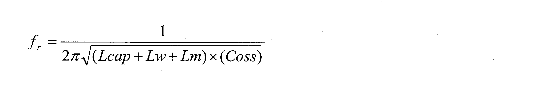
請求項9に記載の電力変換装置。 The inductance included in each closed circuit is:
Inductance Lm of wiring included in the switching element of the arm corresponding to each closed circuit,
An inductance Lcap included in the capacitor;
The switching element of the arm corresponding to each closed circuit and the inductance Lw of the wiring connecting the capacitor,
Frequency f r of the ringing voltage generated to the each closed circuit,
Based on the output capacitance Coss of the switching element that constitutes one of the N arms, the Lm, the Lcap, and the Lw,
The power conversion device according to claim 9. - 前記周波数frの逆数を前記リンギング電圧の周期とし、
前記コントローラは、
前記キャリア信号のリセットに伴って行われる前記スイッチング動作のタイミングが、前記少なくとも2つの閉回路に対応するアーム間で互いに前記周期の略半周期分ずれるように制御する、
請求項14に記載の電力変換装置。 The reciprocal of the frequency f r and the period of the ringing voltage,
The controller is
The timing of the switching operation performed in conjunction with the resetting of the carrier signal is controlled so that the arms corresponding to the at least two closed circuits are shifted from each other by approximately a half cycle of the cycle.
The power conversion device according to claim 14. - 前記複数の閉回路は、それぞれ、U相アーム、V相アームおよびW相アームを含む閉回路であり、
前記周波数frの逆数を前記リンギング電圧の周期とし、
前記コントローラは、
前記U相アームに対し、前記V相アームのスイッチング素子における前記キャリア信号のリセットに伴って行われるスイッチング動作のタイミングを、前記リンギング電圧の略1/3周期遅延させ、かつ、
前記U相アームに対し、前記W相アームのスイッチング素子における前記キャリア信号のリセットに伴って行われるスイッチング動作のタイミングを、前記リンギング電圧の略2/3周期分遅延させる、
請求項14に記載の電力変換装置。 The plurality of closed circuits are closed circuits each including a U-phase arm, a V-phase arm, and a W-phase arm,
The reciprocal of the frequency f r and the period of the ringing voltage,
The controller is
Delaying the timing of the switching operation performed in association with the reset of the carrier signal in the switching element of the V-phase arm with respect to the U-phase arm by approximately 1/3 period of the ringing voltage;
Delaying the timing of the switching operation performed in association with the reset of the carrier signal in the switching element of the W-phase arm by approximately 2/3 period of the ringing voltage with respect to the U-phase arm.
The power conversion device according to claim 14. - 前記電力変換装置は、さらに、
前記リンギング電圧に基づくノイズを検出するノイズ検出部を備え、
前記ノイズ検出部の検出結果に応じて、前記スイッチング動作のタイミングのずれ量を可変とする、
請求項1または請求項9に記載の電力変換装置。 The power conversion device further includes:
A noise detection unit for detecting noise based on the ringing voltage;
According to the detection result of the noise detection unit, the amount of shift in the timing of the switching operation is variable.
The power conversion device according to claim 1 or 9. - 前記ノイズ検出部は、前記電力変換装置の入力端子におけるノイズを検出する、
請求項17に記載の電力変換装置。 The noise detection unit detects noise at an input terminal of the power converter;
The power conversion device according to claim 17. - 前記ノイズ検出部は、前記電力変換装置の出力端子におけるノイズを検出する、
請求項17に記載の電力変換装置。 The noise detection unit detects noise at an output terminal of the power converter;
The power conversion device according to claim 17. - 前記スイッチング素子におけるオンからオフへの遷移時間と、オフからオンへの遷移時間とが同一である、
請求項1または請求項9に記載の電力変換装置。 The transition time from on to off in the switching element is the same as the transition time from off to on.
The power conversion device according to claim 1 or 9. - 前記スイッチング素子は、ワイドバンドギャップ半導体により構成されている、
請求項1または請求項9に記載の電力変換装置。 The switching element is composed of a wide band gap semiconductor,
The power conversion device according to claim 1 or 9.
Priority Applications (4)
| Application Number | Priority Date | Filing Date | Title |
|---|---|---|---|
| JP2012533419A JP5108995B2 (en) | 2010-09-29 | 2011-06-17 | Power converter |
| EP11828276.3A EP2590311A4 (en) | 2010-09-29 | 2011-06-17 | Power converting apparatus |
| CN201180021208.6A CN103222175B (en) | 2010-09-29 | 2011-06-17 | Power converting apparatus |
| US13/641,757 US8885368B2 (en) | 2010-09-29 | 2011-06-17 | Power converting apparatus suppressing switching noise by controlling switching operation |
Applications Claiming Priority (2)
| Application Number | Priority Date | Filing Date | Title |
|---|---|---|---|
| JP2010-218216 | 2010-09-29 | ||
| JP2010218216 | 2010-09-29 |
Publications (1)
| Publication Number | Publication Date |
|---|---|
| WO2012042706A1 true WO2012042706A1 (en) | 2012-04-05 |
Family
ID=45892205
Family Applications (1)
| Application Number | Title | Priority Date | Filing Date |
|---|---|---|---|
| PCT/JP2011/003463 WO2012042706A1 (en) | 2010-09-29 | 2011-06-17 | Power converting apparatus |
Country Status (5)
| Country | Link |
|---|---|
| US (1) | US8885368B2 (en) |
| EP (1) | EP2590311A4 (en) |
| JP (1) | JP5108995B2 (en) |
| CN (1) | CN103222175B (en) |
| WO (1) | WO2012042706A1 (en) |
Cited By (5)
| Publication number | Priority date | Publication date | Assignee | Title |
|---|---|---|---|---|
| JP2013236078A (en) * | 2012-05-03 | 2013-11-21 | Alstom Transport Sa | Device including electronic component with high switching speed |
| JP2016214038A (en) * | 2015-05-13 | 2016-12-15 | 株式会社神戸製鋼所 | Drive unit |
| JP2020048300A (en) * | 2018-09-18 | 2020-03-26 | 株式会社東芝 | Control device, control system, and control method |
| JP2020156208A (en) * | 2019-03-20 | 2020-09-24 | トヨタ自動車株式会社 | Motor system |
| JP7375370B2 (en) | 2019-08-22 | 2023-11-08 | 株式会社デンソー | inverter circuit |
Families Citing this family (30)
| Publication number | Priority date | Publication date | Assignee | Title |
|---|---|---|---|---|
| CN103312240A (en) * | 2013-06-27 | 2013-09-18 | 上海新时达电气股份有限公司 | Three-phase terminal voltage estimation method, back electric motive force estimation method, phase change point detection method and frequency converter for brushless direct current motor |
| DE102014000945A1 (en) * | 2014-01-24 | 2015-07-30 | Brose Fahrzeugteile GmbH & Co. Kommanditgesellschaft, Würzburg | Method of operation and device for controlling a rotating brushless electric machine |
| CN104300819A (en) * | 2014-09-17 | 2015-01-21 | 思源清能电气电子有限公司 | Three-level three-phase bridge circuit and modular structure thereof |
| WO2016093269A1 (en) * | 2014-12-12 | 2016-06-16 | 株式会社ダイヘン | High-frequency power source |
| JP2016135070A (en) * | 2015-01-22 | 2016-07-25 | 株式会社デンソー | Control apparatus |
| US10404188B2 (en) * | 2015-11-16 | 2019-09-03 | Aisin Aw Co., Ltd. | Power conversion devices |
| JP6848183B2 (en) * | 2016-02-16 | 2021-03-24 | 富士電機株式会社 | Current detector and semiconductor device |
| US11251622B1 (en) * | 2016-03-18 | 2022-02-15 | Apple Inc. | Converter employing differing switch types in parallel |
| FR3049785B1 (en) | 2016-04-01 | 2019-08-30 | Alstom Transport Technologies | ELECTRIC POWER CONVERTER, TRACTION CHAIN COMPRISING SUCH A CONVERTER AND ELECTRICAL TRANSPORT VEHICLE THEREFOR |
| JP6623958B2 (en) * | 2016-07-12 | 2019-12-25 | 株式会社デンソー | Drive circuit of the switch to be driven |
| US11271489B2 (en) * | 2016-11-14 | 2022-03-08 | Nidec Corporation | AC-DC power supply and motor |
| JP6873687B2 (en) * | 2016-12-27 | 2021-05-19 | 株式会社京三製作所 | Power supply and control method of power supply |
| JP6947504B2 (en) * | 2016-12-27 | 2021-10-13 | 株式会社京三製作所 | Power supply unit and control method of power supply unit |
| DE102017101359A1 (en) | 2017-01-25 | 2018-07-26 | Wobben Properties Gmbh | Method for feeding an alternating electrical current |
| KR101911269B1 (en) * | 2017-04-24 | 2018-10-24 | 엘지전자 주식회사 | Power transforming apparatus and air conditioner including the same |
| DK3396833T3 (en) | 2017-04-28 | 2019-11-18 | Gn Hearing As | Hearing aid comprising SWITCHED CAPACITOR-DC-DC CONVERTERS WITH LOW ELECTROMAGNETIC EMISSION |
| JP6390807B1 (en) | 2018-03-02 | 2018-09-19 | 富士電機株式会社 | Power converter |
| EP3547525A1 (en) | 2018-03-27 | 2019-10-02 | General Electric Technology GmbH | Voltage source converter apparatus |
| FR3082676B1 (en) | 2018-06-19 | 2021-07-23 | Alstom Transp Tech | ELECTRICAL ENERGY CONVERTER, DRIVE CHAIN INCLUDING SUCH A CONVERTER AND ASSOCIATED ELECTRIC TRANSPORT VEHICLE |
| TWI683522B (en) * | 2018-10-24 | 2020-01-21 | 林景源 | High frequency time-division multi-phase power converter |
| EP3726719A1 (en) * | 2019-04-15 | 2020-10-21 | Infineon Technologies Austria AG | Power converter and power conversion method |
| CN110277909B (en) * | 2019-07-09 | 2022-09-20 | 南京矽力微电子技术有限公司 | Switched capacitor converter, current control circuit and current control method |
| CN112639492A (en) * | 2019-07-24 | 2021-04-09 | 东芝三菱电机产业系统株式会社 | Capacitor diagnosis device and capacitor diagnosis method |
| JP7332382B2 (en) * | 2019-07-31 | 2023-08-23 | サンデン株式会社 | Inverter device |
| US11094807B2 (en) * | 2019-09-05 | 2021-08-17 | Stmicroelectronics S.R.L. | Anti-aging architecture for power MOSFET device |
| JP7166240B2 (en) * | 2019-12-17 | 2022-11-07 | 株式会社東芝 | electronic circuit |
| CN111697957B (en) * | 2020-06-17 | 2024-03-12 | 上海电气集团股份有限公司 | Driving circuit applied to insulated gate bipolar transistor IGBT |
| US20220140748A1 (en) * | 2020-11-05 | 2022-05-05 | Renesas Electronics Corporation | Semiconductor device and inverter device |
| CN113114061B (en) * | 2021-03-26 | 2022-06-24 | 台达电子企业管理(上海)有限公司 | Converter and method for suppressing circulating current interference of converter |
| US11646671B1 (en) * | 2021-10-12 | 2023-05-09 | Utah State University | Unfolder-based single-stage AC-AC conversion system |
Citations (8)
| Publication number | Priority date | Publication date | Assignee | Title |
|---|---|---|---|---|
| JPH07274517A (en) | 1994-03-28 | 1995-10-20 | Central Japan Railway Co | Control device for pwm converter |
| JPH11274901A (en) * | 1998-03-25 | 1999-10-08 | Mitsubishi Electric Corp | Output circuit, pulse width modulation circuit and semiconductor integrated circuit |
| JP2002252985A (en) * | 2000-12-19 | 2002-09-06 | Fuji Electric Co Ltd | Noise reducing apparatus for power converter |
| JP2004364443A (en) * | 2003-06-06 | 2004-12-24 | Daihen Corp | Pulse-width modulated inverter device |
| JP2005218170A (en) * | 2004-01-27 | 2005-08-11 | Nippon Yusoki Co Ltd | Polyphase carrier generator and polyphase carrier generating method |
| JP2006101675A (en) * | 2004-09-30 | 2006-04-13 | Mitsubishi Electric Corp | Motor drive |
| JP2006333647A (en) | 2005-05-27 | 2006-12-07 | Denso Corp | Common mode noise canceling circuit device for vehicle-mounted high-voltage motor device |
| JP2007018617A (en) * | 2005-07-08 | 2007-01-25 | Sharp Corp | Laser diode driving circuit |
Family Cites Families (19)
| Publication number | Priority date | Publication date | Assignee | Title |
|---|---|---|---|---|
| JPH04123520A (en) | 1990-09-14 | 1992-04-23 | Mitsubishi Electric Corp | Output buffer circuit |
| JP3164838B2 (en) * | 1991-06-19 | 2001-05-14 | 株式会社日立製作所 | Switching circuit, conversion device using the same, and power factor improving power supply device |
| JPH06152372A (en) | 1992-11-04 | 1994-05-31 | Toshiba Corp | Semiconductor integrated circuit |
| JPH07327054A (en) | 1994-06-02 | 1995-12-12 | Hitachi Ltd | Pulse transmission method and electronic device or semiconductor device using the method |
| EP1220432A3 (en) | 2000-12-19 | 2003-01-29 | Fuji Electric Co., Ltd. | Noise reduction apparatus for electric power conversion apparatus |
| JP2002199699A (en) * | 2000-12-22 | 2002-07-12 | Fuji Electric Co Ltd | Power conversion device and its driving method |
| JP2003209973A (en) | 2002-01-11 | 2003-07-25 | Meidensha Corp | Power converter |
| JP3864308B2 (en) * | 2002-06-12 | 2006-12-27 | 株式会社安川電機 | PWM inverter control method |
| US7049771B2 (en) | 2004-01-27 | 2006-05-23 | Nippon Yusoki Co., Ltd. | Multi-phase carrier signal generator and multi-phase carrier signal generation method |
| KR100595447B1 (en) | 2004-03-26 | 2006-07-03 | 삼성전자주식회사 | Dc-dc converter and method of controlling the same |
| US7639518B2 (en) * | 2006-04-26 | 2009-12-29 | Nissan Motor Co., Ltd. | Device and method for controlling power converting device |
| KR100813844B1 (en) * | 2006-09-14 | 2008-03-17 | 삼성에스디아이 주식회사 | Asymmetric direct current to direct current converter by using nand gate |
| JP5239234B2 (en) | 2006-10-16 | 2013-07-17 | 日産自動車株式会社 | Power conversion device and power conversion method |
| JP2008109727A (en) | 2006-10-23 | 2008-05-08 | Nippon Soken Inc | Inverter unit |
| WO2008149523A1 (en) * | 2007-05-29 | 2008-12-11 | Panasonic Corporation | Power converter |
| DE102008054487A1 (en) * | 2008-01-09 | 2009-07-16 | DENSO CORPORARTION, Kariya-shi | Control system for a multiphase electric lathe |
| JP5444142B2 (en) * | 2010-07-06 | 2014-03-19 | 株式会社日立製作所 | Power converter and motor drive device using the same |
| JP5333485B2 (en) * | 2011-03-04 | 2013-11-06 | 株式会社デンソー | Power converter |
| EP2792037A2 (en) * | 2011-12-14 | 2014-10-22 | Cirrus Logic, Inc. | Multi-mode flyback control for a switching power converter with dimmer |
-
2011
- 2011-06-17 US US13/641,757 patent/US8885368B2/en not_active Expired - Fee Related
- 2011-06-17 JP JP2012533419A patent/JP5108995B2/en not_active Expired - Fee Related
- 2011-06-17 EP EP11828276.3A patent/EP2590311A4/en not_active Withdrawn
- 2011-06-17 WO PCT/JP2011/003463 patent/WO2012042706A1/en active Application Filing
- 2011-06-17 CN CN201180021208.6A patent/CN103222175B/en not_active Expired - Fee Related
Patent Citations (8)
| Publication number | Priority date | Publication date | Assignee | Title |
|---|---|---|---|---|
| JPH07274517A (en) | 1994-03-28 | 1995-10-20 | Central Japan Railway Co | Control device for pwm converter |
| JPH11274901A (en) * | 1998-03-25 | 1999-10-08 | Mitsubishi Electric Corp | Output circuit, pulse width modulation circuit and semiconductor integrated circuit |
| JP2002252985A (en) * | 2000-12-19 | 2002-09-06 | Fuji Electric Co Ltd | Noise reducing apparatus for power converter |
| JP2004364443A (en) * | 2003-06-06 | 2004-12-24 | Daihen Corp | Pulse-width modulated inverter device |
| JP2005218170A (en) * | 2004-01-27 | 2005-08-11 | Nippon Yusoki Co Ltd | Polyphase carrier generator and polyphase carrier generating method |
| JP2006101675A (en) * | 2004-09-30 | 2006-04-13 | Mitsubishi Electric Corp | Motor drive |
| JP2006333647A (en) | 2005-05-27 | 2006-12-07 | Denso Corp | Common mode noise canceling circuit device for vehicle-mounted high-voltage motor device |
| JP2007018617A (en) * | 2005-07-08 | 2007-01-25 | Sharp Corp | Laser diode driving circuit |
Non-Patent Citations (1)
| Title |
|---|
| See also references of EP2590311A4 * |
Cited By (6)
| Publication number | Priority date | Publication date | Assignee | Title |
|---|---|---|---|---|
| JP2013236078A (en) * | 2012-05-03 | 2013-11-21 | Alstom Transport Sa | Device including electronic component with high switching speed |
| JP2016214038A (en) * | 2015-05-13 | 2016-12-15 | 株式会社神戸製鋼所 | Drive unit |
| JP2020048300A (en) * | 2018-09-18 | 2020-03-26 | 株式会社東芝 | Control device, control system, and control method |
| JP2020156208A (en) * | 2019-03-20 | 2020-09-24 | トヨタ自動車株式会社 | Motor system |
| JP7156118B2 (en) | 2019-03-20 | 2022-10-19 | 株式会社デンソー | motor system |
| JP7375370B2 (en) | 2019-08-22 | 2023-11-08 | 株式会社デンソー | inverter circuit |
Also Published As
| Publication number | Publication date |
|---|---|
| CN103222175A (en) | 2013-07-24 |
| JPWO2012042706A1 (en) | 2014-02-03 |
| EP2590311A4 (en) | 2014-04-23 |
| EP2590311A1 (en) | 2013-05-08 |
| US20130039100A1 (en) | 2013-02-14 |
| JP5108995B2 (en) | 2012-12-26 |
| CN103222175B (en) | 2015-07-01 |
| US8885368B2 (en) | 2014-11-11 |
Similar Documents
| Publication | Publication Date | Title |
|---|---|---|
| JP5108995B2 (en) | Power converter | |
| Nguyen et al. | A new SVM method for an indirect matrix converter with common-mode voltage reduction | |
| US8680794B2 (en) | Load drive system, motor drive system, and vehicle control system | |
| JP6319824B2 (en) | Multi-level inverter device and method of operation | |
| JP6206502B2 (en) | Power conversion device and power conversion method | |
| US9071166B2 (en) | Power converter with surge voltage suppression | |
| WO2011033698A1 (en) | Power converter | |
| EP3358733A1 (en) | Power conversion device | |
| Mookken et al. | Efficient and compact 50kW Gen2 SiC device based PV string inverter | |
| WO2017038022A1 (en) | Power conversion device | |
| JP6168155B2 (en) | Power conversion device and power conversion method | |
| KR102387744B1 (en) | AC-AC converter circuit | |
| JP4873317B2 (en) | Inverter device | |
| Ko et al. | Modulation strategy for highly reliable cascade H-Bridge inverter based on discontinuous PWM | |
| CN108471247B (en) | Control method, device and system of three-level inverter | |
| JP2011160570A (en) | Switching control device | |
| JP2015042076A (en) | Power conversion device | |
| CN110447163B (en) | Power conversion device | |
| JP7402009B2 (en) | PWM control inverter | |
| US9800133B2 (en) | Active common mode cancellation | |
| JP6191542B2 (en) | Power converter | |
| KR101422961B1 (en) | Driver device for power factor correction circuit | |
| JP2017042040A (en) | Power conversion device | |
| JP2021168534A (en) | Power conversion device | |
| JP5894031B2 (en) | Power converter |
Legal Events
| Date | Code | Title | Description |
|---|---|---|---|
| 121 | Ep: the epo has been informed by wipo that ep was designated in this application |
Ref document number: 11828276 Country of ref document: EP Kind code of ref document: A1 |
|
| WWE | Wipo information: entry into national phase |
Ref document number: 2012533419 Country of ref document: JP |
|
| WWE | Wipo information: entry into national phase |
Ref document number: 2011828276 Country of ref document: EP |
|
| WWE | Wipo information: entry into national phase |
Ref document number: 13641757 Country of ref document: US |
|
| NENP | Non-entry into the national phase |
Ref country code: DE |