JP2008109727A - Inverter unit - Google Patents
Inverter unit Download PDFInfo
- Publication number
- JP2008109727A JP2008109727A JP2006287510A JP2006287510A JP2008109727A JP 2008109727 A JP2008109727 A JP 2008109727A JP 2006287510 A JP2006287510 A JP 2006287510A JP 2006287510 A JP2006287510 A JP 2006287510A JP 2008109727 A JP2008109727 A JP 2008109727A
- Authority
- JP
- Japan
- Prior art keywords
- pwm control
- control signal
- inverter
- signal generator
- group
- Prior art date
- Legal status (The legal status is an assumption and is not a legal conclusion. Google has not performed a legal analysis and makes no representation as to the accuracy of the status listed.)
- Pending
Links
Images


Landscapes
- Power Conversion In General (AREA)
- Inverter Devices (AREA)
Abstract
Description
本発明は、インバータ装置に関し、特にそのスイッチングノイズの低減に関する。 The present invention relates to an inverter device, and more particularly to reduction of the switching noise.
PWM制御などにより形成されて主として交流モータ駆動用の交流電圧を形成するインバータ装置では高周波のスイッチングノイズ(以下、インバータノイズとも称する)が発生する。このインバータノイズは、電源ラインを通じて直流電源系に悪影響を与えたり、電磁波ノイズを周囲に放射したりするため、極力低減する必要がある。 High frequency switching noise (hereinafter also referred to as inverter noise) is generated in an inverter device that is formed by PWM control or the like and mainly forms an AC voltage for driving an AC motor. This inverter noise needs to be reduced as much as possible because it adversely affects the DC power supply system through the power supply line and radiates electromagnetic noise to the surroundings.
特許文献1は、それぞれ三相インバータである第1モータ駆動用の第1インバータと第2モータ駆動用の第2インバータとを駆動制御するPWM信号発生器を共用化することにより、第1モータ駆動用の第1インバータの上アーム素子のオンと、第2モータ駆動用の第2インバータの下アーム素子のオンとを同期させ、第1モータ駆動用の第1インバータの下アーム素子のオンと、第2モータ駆動用の第2インバータの上アーム素子のオンとを同期させることにより、スイッチングノイズを低減できることを主張している。更に詳しく説明すると、この技術では、第1インバータは上アーム素子U1、V1、W1、下アーム素子X1、Y1、Z1をもち、第2インバータは上アーム素子U2、V2、W2、下アーム素子X2、Y2、Z2をもつ。スイッチング素子U1、X2のペア、スイッチング素子V1、Y2のペア、スイッチング素子W1、Z2のペア、スイッチング素子Y1、V2のペア、スイッチング素子Z1、W2のペアを、ペアごとに同期してオン、オフさせる。
しかしながら、上記した従来技術のスイッチングノイズキャンセル技術では、2台のモータが、常に同時運転されるとともに、両モータの出力すなわちPWMデューテイ比が相補関係に固定されてしまうため、実用性に大きな問題があった。更に、2個のモータの巻線とグランドとの間の浮遊容量の大きさが異なると浮遊容量を通じて外部に流れるコモンモードノイズ電流に差が生じ、そのキャンセル効果は小さくなってしまう。 However, with the above-described switching noise canceling technology of the prior art, the two motors are always operated simultaneously, and the outputs of both motors, that is, the PWM duty ratio is fixed in a complementary relationship. there were. Furthermore, if the stray capacitances between the windings of the two motors and the ground are different, a difference occurs in the common mode noise current that flows to the outside through the stray capacitance, and the canceling effect is reduced.
本発明は上記問題点に鑑みなされたものであり、複数のモータを個別にPWM駆動する際のインバータスイッチングに起因するノイズを実質的に良好に低減可能なモータ制御装置を提供することをその目的としている。 The present invention has been made in view of the above problems, and an object of the present invention is to provide a motor control device capable of substantially satisfactorily reducing noise caused by inverter switching when a plurality of motors are individually PWM-driven. It is said.
上記課題を解決するための本発明は、それぞれスイッチング素子である上アーム素子と下アーム素子とを直列接続してなるハーフブリッジを相数分並列接続して構成されるとともに共通直流電源から給電されるインバータをそれぞれ少なくとも一つ含む複数のインバータ群と、PWM制御信号を出力するPWM制御信号発生器をそれぞれ少なくとも一つ含み前記複数のインバータ群に前記PWM制御信号を個別に出力する複数のPWM制御信号発生器群と、前記PWM制御信号を作成するためのキャリヤ信号を前記複数のPWM制御信号発生器群に出力するキャリヤ信号発生器とを備える複数モータ制御装置において、前記複数のPWM制御信号発生器群が、周波数が等しく、かつ、互いに位相が異なるキャリヤ信号を基礎とする前記PWM制御信号を前記インバータ群に個別に出力することを特徴としている。以下、説明を簡単とするため、各インバータ群がそれぞれ一個のインバータからなる場合を例として説明する。 In order to solve the above problems, the present invention comprises a half bridge formed by connecting an upper arm element and a lower arm element, which are switching elements, in series, connected in parallel for the number of phases and fed from a common DC power source. A plurality of inverter groups each including at least one inverter, and a plurality of PWM controls each including at least one PWM control signal generator for outputting a PWM control signal and individually outputting the PWM control signal to the plurality of inverter groups In a plurality of motor control devices comprising a signal generator group and a carrier signal generator that outputs a carrier signal for generating the PWM control signal to the plurality of PWM control signal generator groups, the plurality of PWM control signal generations The PWM is based on carrier signals having the same frequency and different phases It is characterized by outputting individually control signal to said inverter group. Hereinafter, in order to simplify the description, a case where each inverter group is composed of one inverter will be described as an example.
すなわち、この発明は、複数のインバータに印加するPWM制御信号の周波数を等しくし、位相をずらせる。好適には、各インバータのスイッチングノイズ電力が最小となる位相が選択される。以下、三相インバータを例として具体的に説明すると、2つの三相インバータの同一相同アーム側のスイッチング素子に印加されるPWM制御信号の位相は、各インバータの同一相同アーム側のスイッチング素子のスイッチングノイズ電力が好適には最小となるように位相がシフトされる。これにより、各インバータの同一相同アーム側のスイッチング素子のオン期間がこの位相分だけずれるため、それによる合成スイッチングノイズの振幅を低減できる。これにより、電源ラインを通じてあるいは電磁波として外部に出力されるスイッチングノイズの影響を簡素な回路構成により低減することができる。また、合成スイッチングノイズの周波数は等価的に増大するため、たとえば直流電源と並列接続された平滑コンデンサによるスイッチングノイズ電流の吸収効果も向上することができる。 That is, according to the present invention, the frequencies of the PWM control signals applied to the plurality of inverters are made equal to shift the phase. Preferably, the phase that minimizes the switching noise power of each inverter is selected. The phase of the PWM control signal applied to the switching elements on the same homologous arm side of the two three-phase inverters is the switching of the switching elements on the same homologous arm side of each inverter. The phase is shifted so that the noise power is preferably minimized. As a result, the ON period of the switching element on the same homologous arm side of each inverter is shifted by this phase, so that the amplitude of the resultant switching noise can be reduced. As a result, the influence of switching noise output to the outside through the power line or as electromagnetic waves can be reduced with a simple circuit configuration. In addition, since the frequency of the combined switching noise increases equivalently, for example, the effect of absorbing the switching noise current by a smoothing capacitor connected in parallel with the DC power supply can be improved.
好適な態様において、前記キャリヤ信号発生器は、互いに位相が異なり、周波数が等しい複数のキャリヤ信号を前記複数のPWM制御信号発生器群に個別に出力する。これにより、各インバータ群に出力する複数のPWM制御信号の位相を簡素に相対シフトすることができる。なお、各PWM制御信号間の位相シフトのその他の態様としては、同一周期、同一位相のキャリヤ信号からPWM制御信号を形成する各PWM制御信号発生器内に、キャリヤ信号の位相あるいは形成したPWM制御信号の位相をシフトする回路を個別に組み込むことも可能である。 In a preferred aspect, the carrier signal generator individually outputs a plurality of carrier signals having different phases and equal frequencies to the plurality of PWM control signal generator groups. Thereby, the phase of the some PWM control signal output to each inverter group can be simply shifted relatively. As another aspect of the phase shift between the PWM control signals, the phase of the carrier signal or the PWM control formed is formed in each PWM control signal generator that forms the PWM control signal from the carrier signal having the same period and the same phase. It is also possible to incorporate a circuit for shifting the phase of the signal individually.
好適な態様において、前記複数のインバータ群は、第1インバータ群と第2インバータ群とを有し、
前記複数のPWM制御信号発生器群は、前記第1インバータ群に前記PWM制御信号を出力する第1PWM制御信号発生器群と、前記第2インバータ群に前記PWM制御信号を出力する第2PWM制御信号発生器群とを有し、前記キャリヤ信号発生器は、前記第1PWM制御信号発生器群に出力するキャリヤ信号を、前記第2PWM制御信号発生器群に出力するキャリヤ信号に対して位相を略180度をずらせる。このようにすれば、上記した合成スイッチングノイズを示すベクトルの長さすなわち振幅を最も減少させることができる。たとえば、PWMのオンデューティ比(以下、単にデューティとも言う)が50%近傍において、第1、第2のインバータの同一相同一アームのスイッチング素子は交互に連続してオンすることになり、その結果、一方のスイッチング素子のオン遷移期間に他方のスイッチング素子のオフ遷移期間が重なることになり、優れたコモンモードノイズ相殺効果が得られる。
In a preferred aspect, the plurality of inverter groups include a first inverter group and a second inverter group,
The plurality of PWM control signal generator groups include a first PWM control signal generator group that outputs the PWM control signal to the first inverter group, and a second PWM control signal that outputs the PWM control signal to the second inverter group. The carrier signal generator has a phase of about 180 with respect to the carrier signal output to the first PWM control signal generator group with respect to the carrier signal output to the second PWM control signal generator group. Shift the degree. In this way, the length, that is, the amplitude of the vector indicating the above-described combined switching noise can be reduced most. For example, when the PWM on-duty ratio (hereinafter also simply referred to as duty) is in the vicinity of 50%, the switching elements of the same phase and the same arm of the first and second inverters are alternately turned on continuously. Thus, the off transition period of the other switching element overlaps the on transition period of one switching element, and an excellent common mode noise canceling effect is obtained.
好適な態様において、前記キャリヤ信号発生器は、前記第1PWM制御信号発生器群に出力するキャリヤ信号を反転して前記第2PWM制御信号発生器群に出力するキャリヤ信号とする。このようにすれば、上記した180度位相シフトを簡単な回路で実行することができる。 In a preferred aspect, the carrier signal generator inverts the carrier signal output to the first PWM control signal generator group to be a carrier signal output to the second PWM control signal generator group. In this way, the above 180 degree phase shift can be executed with a simple circuit.
好適な態様において、前記複数のインバータ群は、第1インバータ群と第2インバータ群と第3インバータ群とを有し、前記複数のPWM制御信号発生器群は、前記第1インバータ群に前記PWM制御信号を出力する第1PWM制御信号発生器群と、前記第2インバータ群に前記PWM制御信号を出力する第2PWM制御信号発生器群と、前記第3インバータ群に前記PWM制御信号を出力する第3PWM制御信号発生器群とを有し、前記キャリヤ信号発生器は、前記第1PWM制御信号発生器群に出力するキャリヤ信号と、前記第2PWM制御信号発生器群に出力するキャリヤ信号と、前記第3PWM制御信号発生器群に出力するキャリヤ信号とを間の位相を略120度ずらせる。このようにすれば、これら3つのPWM制御信号を同一位相で出力するのに比較して合成スイッチングノイズを格段に低減することができる。たとえば、PWMのオンデューティ比(以下、単にデューティとも言う)が33%近傍において、第1〜第3のインバータの同一相同一アームのスイッチング素子は交互に連続してオンすることになり、その結果、一つのスイッチング素子のオン遷移期間に他のスイッチング素子のオフ遷移期間が重なることになり、優れたコモンモードノイズ相殺効果が得られる。また、たとえ上記した各スイッチング素子のオン遷移期間とオフ遷移期間とが重ならなくても、それらが、時間的に分散することにより合成スイッチングノイズ電力の振幅低減と高周波化による既述の効果は実現することができる。 In a preferred aspect, the plurality of inverter groups include a first inverter group, a second inverter group, and a third inverter group, and the plurality of PWM control signal generator groups are connected to the first inverter group by the PWM. A first PWM control signal generator group that outputs a control signal; a second PWM control signal generator group that outputs the PWM control signal to the second inverter group; and a second PWM control signal that outputs the PWM control signal to the third inverter group. 3 PWM control signal generator group, and the carrier signal generator outputs a carrier signal output to the first PWM control signal generator group, a carrier signal output to the second PWM control signal generator group, and the first The phase of the carrier signal output to the 3PWM control signal generator group is shifted by approximately 120 degrees. In this way, compared with outputting these three PWM control signals with the same phase, the combined switching noise can be significantly reduced. For example, when the PWM on-duty ratio (hereinafter also simply referred to as duty) is around 33%, the switching elements of the same phase and the same arm of the first to third inverters are alternately turned on continuously, and as a result. Thus, the off transition period of another switching element overlaps the on transition period of one switching element, and an excellent common mode noise canceling effect can be obtained. Moreover, even if the above-described on-transition period and off-transition period of each switching element do not overlap, the above-described effects due to the reduction in amplitude and increase in the frequency of the combined switching noise power due to the temporal dispersion of the switching elements Can be realized.
好適な態様において、前記複数のインバータ群の出力端と接地との間の対地寄生容量の差異を低減するコンデンサを、前記対地寄生容量が小さい前記複数のインバータ群の出力端と接地との間に付加することにより、前記複数のインバータ群の前記対地寄生容量の差異を低減する。なお、ここで言うインバータ群又はインバータの出力端と接地との間の対地寄生容量とは、インバータから給電される電気負荷たとえばモータの対地寄生容量を含む。このようにすれば、インバータのスイッチングにより形成された対地絶縁方式のインバータ及び電気負荷にそれらの対地静電容量を通じて流れる電流(以下、コモンモードノイズ電流とも言う)を良好に平均化することができる。たとえば、PWMのオンデューティ比(以下、単にデューティとも言う)が50%近傍において、第1、第2のインバータの同一相同一アームのスイッチング素子は交互に連続してオンすることになり、その結果、一方のスイッチング素子のオン遷移期間に他方のスイッチング素子のオフ遷移期間が重なることになり、優れたコモンモードノイズ相殺効果が得られる。 In a preferred aspect, a capacitor for reducing a difference in ground parasitic capacitance between the output terminals of the plurality of inverter groups and the ground is provided between the output terminals of the plurality of inverter groups having a small ground parasitic capacity and the ground. By adding, the difference in the ground parasitic capacitance of the plurality of inverter groups is reduced. Here, the ground parasitic capacitance between the inverter group or the output terminal of the inverter and the ground includes an electric load fed from the inverter, for example, a ground parasitic capacitance of a motor. In this way, it is possible to satisfactorily average the current (hereinafter also referred to as common mode noise current) flowing through the ground capacitance to the ground insulation type inverter formed by switching of the inverter and the electric load. . For example, when the PWM on-duty ratio (hereinafter also simply referred to as duty) is in the vicinity of 50%, the switching elements of the same phase and the same arm of the first and second inverters are alternately turned on continuously. Thus, the off transition period of the other switching element overlaps the on transition period of one switching element, and an excellent common mode noise canceling effect is obtained.
好適な態様において、前記複数のインバータ群の入力端から見た前記複数のインバータ群の対地寄生容量の差が最も小さくなるように前記複数のインバータ群から給電される電気負荷を組み合わせる。このようにすれば、インバータのスイッチングにより形成された対地絶縁方式のインバータ及び電気負荷にそれらの対地静電容量を通じて流れるコモンモードノイズ電流を良好に平均化することができる。たとえば、PWMのオンデューティ比(以下、単にデューティとも言う)が50%近傍において、第1、第2のインバータの同一相同一アームのスイッチング素子は交互に連続してオンすることになり、その結果、一方のスイッチング素子のオン遷移期間に他方のスイッチング素子のオフ遷移期間が重なることになり、優れたコモンモードノイズ相殺効果が得られる。 In a preferred aspect, the electric loads fed from the plurality of inverter groups are combined so that the difference in ground parasitic capacitance between the plurality of inverter groups viewed from the input terminals of the plurality of inverter groups is minimized. In this way, it is possible to satisfactorily average the common mode noise current flowing through the ground capacitance to the ground insulation type inverter formed by switching of the inverter and the electric load. For example, when the PWM on-duty ratio (hereinafter also simply referred to as duty) is in the vicinity of 50%, the switching elements of the same phase and the same arm of the first and second inverters are alternately turned on continuously. Thus, the off transition period of the other switching element overlaps the on transition period of one switching element, and an excellent common mode noise canceling effect is obtained.
本発明の望ましい実施態様を図面を参照して以下に説明する。ただし、既述した本発明の技術思想は、下記の実施態様に限定解釈されるべきものでなく、その他の公知技術を組み合わせて実施しても良いことは当然である。 Preferred embodiments of the present invention will be described below with reference to the drawings. However, the technical idea of the present invention described above should not be construed as being limited to the following embodiments, and may naturally be implemented in combination with other known techniques.
(実施形態1)
実施形態1の複数モータ制御装置を図1を参照して以下に説明する。
(Embodiment 1)
The multiple motor control apparatus of
(回路構成)
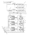
実施形態1の複数モータ制御装置を図1に示すブロック回路図を参照して説明する。この実施形態は、それぞれ1つのインバータからなる2つのインバータ群に適用される。
(Circuit configuration)
The multiple motor control apparatus of
図1において、1、2は三相交流モータ、3、4は三相インバータからなるインバータ、5、6はPWM制御信号生成部(本発明で言うPWM制御信号発生器)、7はキャリヤ信号生成部(本発明で言うキャリヤ信号発生器の一部)、8は信号電圧を反転する反転回路(本発明で言うキャリヤ信号発生器の残部)、9は一対の電源ラインの対地寄生容量(浮遊容量)、10は対地絶縁された直流電源、11はグラウンド、12、13は三相交流モータ1、2の各相ステータコイルの対地静電容量(浮遊容量)、14は直流電源10と並列接続された平滑コンデンサであり、浮遊容量12、13は、それぞれインバータ3、4から三相交流モータ1、2へ至る交流配線の対地寄生容量を含む。三相交流モータ1、2を除く上記各回路部は本発明で言う複数モータ制御装置を構成している。
In FIG. 1, 1 and 2 are three-phase AC motors, 3 and 4 are inverters composed of three-phase inverters, 5 and 6 are PWM control signal generators (PWM control signal generators referred to in the present invention), and 7 is a carrier signal generator. (A part of the carrier signal generator in the present invention), 8 is an inverting circuit for inverting the signal voltage (the remainder of the carrier signal generator in the present invention), and 9 is a ground parasitic capacitance (floating capacitance) of a pair of power supply lines. ) 10 is a grounded DC power source, 11 is ground, 12 and 13 are ground capacitances (floating capacitances) of the respective phase stator coils of the three-
三相交流モータ1、2は、たとえば三相同期モータや三相交流モータにより構成される。もちろん、相数はこれに限定されるものではない。インバータ3、4は、それぞれ半導体スイッチング素子からなる3つの上アーム素子と3つの下アーム素子とを有し、ひとつの上アーム素子とひとつの下アーム素子とは直列接続されてひとつのハーフブリッジ回路を構成している。インバータ3、4は直流電源10から直流電力を給電されている。インバータ3は形成した三相交流電圧を三相交流モータ1の各相のステータコイルに印加している。インバータ4は形成した三相交流電圧を三相交流モータ2の各相のステータコイルに給電している。
The three-
キャリヤ信号生成部7は、たとえば数十KHzの周波数の三角波電圧を第1キャリヤ信号として発生させ、PWM制御信号生成部5に出力する。また、反転回路8は入力された三角波電圧を反転して第2キャリヤ信号としてPWM制御信号生成部6に出力する。PWM制御信号生成部5は、入力された第1キャリヤ信号に基づいて6つのPWM相制御信号からなる第1PWM制御信号を形成し、インバータ3の各アーム素子の制御電極に個別に印加する。PWM制御信号生成部6は、入力された第2キャリヤ信号に基づいて6つのPWM相制御信号からなる第2PWM制御信号を形成し、インバータ4の各アーム素子の制御電極に個別に印加する。
The carrier
第1PWM制御信号及び第2PWM制御信号の波形は、PWM制御方式において種々異なる。PWM制御方式としては、120度通電方式、180度通電方式、2相変調方式など各種の方式が知られている。典型的には、第1PWM相制御信号の3つの上アーム素子制御用のPWM相制御信号は120度位相がずれている。上記した各種PWM制御方式の詳細とそれに対応したPWM制御信号の形成自体は周知であり、かつ、この実施形態の要旨でもないため、これ以上の説明は省略する。 The waveforms of the first PWM control signal and the second PWM control signal are different in the PWM control method. As the PWM control method, various methods such as a 120-degree conduction method, a 180-degree conduction method, and a two-phase modulation method are known. Typically, the PWM phase control signals for controlling the three upper arm elements of the first PWM phase control signal are 120 degrees out of phase. The details of the various PWM control methods described above and the formation of the PWM control signal corresponding to the details are well known and are not the gist of this embodiment, and thus further explanation is omitted.
(動作説明)
以下、上記複数モータ制御装置の動作を説明する。よく知られているように、PWM制御信号生成部5は、入力された第1キャリヤ信号としての三角波電圧を所定のしきい値電圧と比較するコンパレータを有し、コンパレータから出力されるパルス信号乃至それに基づいて形成した6つのパルス信号を上記PWM相制御信号としてインバータ3の各アーム素子に分配する。同じく、PWM制御信号生成部6は、入力された第2キャリヤ信号としての三角波電圧を所定のしきい値電圧と比較するコンパレータを有し、コンパレータから出力されるパルス信号乃至それに基づいて形成した6つのパルス信号を上記PWM相制御信号としてインバータ4の各アーム素子に分配する。この結果、上記しきい値電圧を所定波形に基づいて変調することにより、それに応じたPWM制御信号を得ることができる。
(Description of operation)
Hereinafter, the operation of the multiple motor control device will be described. As is well known, the PWM control
この実施形態では、PWM制御信号生成部6に入力される第2キャリヤ信号は、PWM制御信号生成部5に入力される第1キャリヤ信号と180度位相がずれ、同一周期とされているため、たとえば、インバータ3とインバータ4との同一相同アーム側のスイッチング素子に印加されるパルス信号であるPWM相制御信号の位相が反対となる。このことは、インバータ3のスイッチングノイズ電力とインバータ4のスイッチングノイズ電力との時間的な重なりが最小となり、その分だけ、それらを合成した合成スイッチングノイズ電力が小さくなり、合成スイッチング周波数が倍増することを意味する。その結果、この合成スイッチングノイズが直流電源10やモータ1、2、さらには近傍の電気機器へ与える影響を大幅に軽減できることを意味する。
In this embodiment, the second carrier signal input to the PWM control
このスイッチングノイズ低減効果は、特にPWMオンデューティ比が約50%近傍にて特に効果的となる。たとえば、2つのインバータ3、4をデューティ50%で運転するモータ運転条件において、インバータ3のオン遷移期間は、インバータ4の同一相同アームのスイッチング素子のオフ遷移期間と重なり、インバータ3のオフ遷移期間は、インバータ4の同一相同アームのスイッチング素子のオン遷移期間と重なることになる。したがって、スイッチングノイズ特に、インバータ3、4のスイッチングに伴い、対地寄生容量(浮遊容量)9、12、13及びグラウンド11を通じて流れるコモンモードノイズ電流を大幅に相殺することができる。なお、デューティ50%近傍にて運転しない場合であっても、しきい値電圧(交流電圧の瞬時値)が0値近傍となる期間はデューティが50%近傍となるため、上記効果は特に顕著となる。
This switching noise reduction effect is particularly effective when the PWM on-duty ratio is about 50%. For example, in a motor operating condition in which two
(変形態様)
上記実施形態では、反転回路8によりPWM制御信号生成部6へ入力する第2キャリヤ信号の位相を180度ずらせたが、この位相の相対シフトはPWM制御信号生成部6内にて行っても良い。
(Modification)
In the above embodiment, the phase of the second carrier signal input to the PWM control
(変形態様)
上記実施形態では、インバータ3、4は、三相交流モータ1、2に給電したが、その代わりに電動動作と発電動作とを適宜切り替えて行う三相交流発電電動機に給電してもよい。
(Modification)
In the above embodiment, the
(実施形態2)
実施形態2の複数モータ制御装置を図2を参照して以下に説明する。
(Embodiment 2)
The multiple motor control apparatus of
この実施形態は、図1の回路においてインバータ4の三相出力端とグラウンドとの間にそれぞれバランスコンデンサ15を接続した点をその特徴としている。ただし、三相交流モータ1の各相の浮遊容量12は、ほぼ三相交流モータ2の各相の浮遊容量13とバランスコンデンサ15の容量との合計にほぼ等しくされる。このようにすれば、インバータ3、4のスイッチングにより浮遊容量(正確にはインバータ出力側浮遊容量)を通じてグラウンドに流れるノイズ電流(コモンモードノイズ電流と称する)は、両インバータ3、4のオンデューティ比が等しい場合にほぼ等しくなり、既述したようにオンデューティ比が50%近傍において逆位相となるため大幅に相殺することができる。
This embodiment is characterized in that a
(実施形態3)
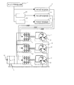
実施形態3の複数モータ制御装置を図3を参照して以下に説明する。
(Embodiment 3)
A multi-motor control apparatus according to
この実施形態は、図1の回路において、PWM制御信号生成部(本発明で言うPWM制御信号発生器)16、インバータ17、三相交流モータ18を追加した点にその特徴がある。更に詳しく説明すると、PWM制御信号生成部16にはキャリヤ信号生成部7から第1キャリヤ信号が入力される。インバータ17は、入力されたPWM制御信号生成部16に基づいて形成した三相交流電圧を三相交流モータ18に印加する。19は三相交流モータ18の各相の浮遊容量である。
This embodiment is characterized in that a PWM control signal generation unit (PWM control signal generator referred to in the present invention) 16, an
ただし、この実施形態では、三相交流モータ2の浮遊容量13はほぼ、三相交流モータ1の浮遊容量12と三相交流モータ18の浮遊容量19の和にほぼ等しくなっている。このようにすれば、図2で説明したバランスコンデンサ15を省略乃至大幅に小型化したとしても、インバータ3、17のスイッチングに伴うコモンモードノイズ電流と、インバータ4のスイッチングに伴うコモンモードノイズ電流の大きさをほぼ等しくかつ逆相とすることができる。
However, in this embodiment, the
(実施形態4)
実施形態4の複数モータ制御装置を図3を参照して以下に説明する。
(Embodiment 4)
A multi-motor control apparatus according to
この実施形態は、図3の回路において、反転回路8を省略する代わりに、キャリヤ信号生成部7から出力される第1キャリヤ信号の位相をπ/3シフトして第2キャリヤ信号とする位相シフト回路81と、キャリヤ信号生成部7から出力される第1キャリヤ信号の位相を2π/3シフトして第3キャリヤ信号とする位相シフト回路82とを設けたものである。なお、この実施形態では、各三相交流モータ1、2、18の浮遊容量12、13、19は略等しいと仮定する。
In this embodiment, instead of omitting the
第2キャリヤ信号はPWM制御信号生成部16に入力され、第3キャリヤ信号はPWM制御信号生成部6に入力される。これにより、各PWM制御信号生成部5、6、16が出力する各PWM制御信号は同一周波数にて位相が約120度ずつずれていることになる。このようにすれば、3つのインバータ3、4、17が出力するスイッチングノイズを時間的に均等分散するため既述の合成スイッチングノイズ低減効果並びにコモンモードノイズを良好に低減することができる。特にこれらの効果は、オンデューティ比が33%程度の場合に顕著となる。
The second carrier signal is input to the PWM control
(実験例)
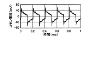
実施形態2によるコモンモードノイズ電流波形を図5に示し、実施形態2にて第1、第2キャリヤ信号の位相を一致させた場合のコモンモードノイズ電流波形を図6に示す。PWM制御信号のオンデューティ比は50%、二つの浮遊容量9はそれぞれ40nF、三相交流モータ1の浮遊容量12は12nF、三相交流モータ2の浮遊容量13は4nF、バランスコンデンサ容量15は一相あたり2.7nFである。図5、図6からコモンモードノイズ電流の大幅な低減が実現できたことがわかる。
(Experimental example)
FIG. 5 shows a common mode noise current waveform according to the second embodiment, and FIG. 6 shows a common mode noise current waveform when the phases of the first and second carrier signals are matched in the second embodiment. The on-duty ratio of the PWM control signal is 50%, the two
1 三相交流モータ
2 三相交流モータ
3 インバータ
4 インバータ
5 PWM制御信号生成部
6 PWM制御信号生成部
7 キャリヤ信号生成部
8 反転回路
9 浮遊容量
10 直流電源
11 グラウンド
12 浮遊容量
13 浮遊容量
15 バランスコンデンサ
16 PWM制御信号生成部
17 インバータ
18 三相交流モータ
19 浮遊容量
81 位相シフト回路
82 位相シフト回路
DESCRIPTION OF
Claims (7)
PWM制御信号を出力するPWM制御信号発生器をそれぞれ少なくとも一つ含み前記複数のインバータ群に前記PWM制御信号を個別に出力する複数のPWM制御信号発生器群と、
前記PWM制御信号を作成するためのキャリヤ信号を前記複数のPWM制御信号発生器群に出力するキャリヤ信号発生器と、
を備える複数モータ制御装置において、
前記複数のPWM制御信号発生器群は、
周波数が等しく、かつ、互いに位相が異なるキャリヤ信号を基礎とする前記PWM制御信号を前記インバータ群に個別に出力することを特徴とする複数モータ制御装置。 A plurality of inverters each including at least one inverter fed from a common DC power source and configured by parallelly connecting half bridges, each of which is a switching element, connected in series to each other in number of phases. Group,
A plurality of PWM control signal generator groups each including at least one PWM control signal generator for outputting a PWM control signal and individually outputting the PWM control signal to the plurality of inverter groups;
A carrier signal generator for outputting a carrier signal for generating the PWM control signal to the plurality of PWM control signal generator groups;
In a multiple motor control device comprising:
The plurality of PWM control signal generator groups are:
A multi-motor control device that individually outputs the PWM control signals based on carrier signals having the same frequency and different phases to each other to the inverter group.
前記キャリヤ信号発生器は、
互いに位相が異なり、周波数が等しい複数のキャリヤ信号を前記複数のPWM制御信号発生器群に個別に出力することを特徴とする複数モータ制御装置。 The multiple motor control device according to claim 1,
The carrier signal generator is
A plurality of motor control devices, wherein a plurality of carrier signals having different phases and equal frequencies are individually output to the plurality of PWM control signal generator groups.
前記複数のインバータ群は、第1インバータ群と第2インバータ群とを有し、
前記複数のPWM制御信号発生器群は、前記第1インバータ群に前記PWM制御信号を出力する第1PWM制御信号発生器群と、前記第2インバータ群に前記PWM制御信号を出力する第2PWM制御信号発生器群とを有し、
前記キャリヤ信号発生器は、前記第1PWM制御信号発生器群に出力するキャリヤ信号を、前記第2PWM制御信号発生器群に出力するキャリヤ信号に対して位相を略180度をずらせる複数モータ制御装置。 The multiple motor control device according to claim 2,
The plurality of inverter groups include a first inverter group and a second inverter group,
The plurality of PWM control signal generator groups include a first PWM control signal generator group that outputs the PWM control signal to the first inverter group, and a second PWM control signal that outputs the PWM control signal to the second inverter group. A generator group,
The carrier signal generator is configured to shift a phase of a carrier signal output to the first PWM control signal generator group to about 180 degrees with respect to a carrier signal output to the second PWM control signal generator group. .
前記キャリヤ信号発生器は、前記第1PWM制御信号発生器群に出力するキャリヤ信号を反転して前記第2PWM制御信号発生器群に出力するキャリヤ信号とする複数モータ制御装置。 In the multiple motor control device according to claim 3,
The multi-motor control device, wherein the carrier signal generator inverts a carrier signal output to the first PWM control signal generator group to be a carrier signal output to the second PWM control signal generator group.
前記複数のインバータ群は、第1インバータ群と第2インバータ群と第3インバータ群とを有し、
前記複数のPWM制御信号発生器群は、前記第1インバータ群に前記PWM制御信号を出力する第1PWM制御信号発生器群と、前記第2インバータ群に前記PWM制御信号を出力する第2PWM制御信号発生器群と、前記第3インバータ群に前記PWM制御信号を出力する第3PWM制御信号発生器群とを有し、
前記キャリヤ信号発生器は、前記第1PWM制御信号発生器群に出力するキャリヤ信号と、前記第2PWM制御信号発生器群に出力するキャリヤ信号と、前記第3PWM制御信号発生器群に出力するキャリヤ信号とを間の位相を略120度ずらせる複数モータ制御装置。 The multiple motor control device according to claim 2,
The plurality of inverter groups include a first inverter group, a second inverter group, and a third inverter group,
The plurality of PWM control signal generator groups include a first PWM control signal generator group that outputs the PWM control signal to the first inverter group, and a second PWM control signal that outputs the PWM control signal to the second inverter group. A generator group, and a third PWM control signal generator group that outputs the PWM control signal to the third inverter group,
The carrier signal generator includes a carrier signal output to the first PWM control signal generator group, a carrier signal output to the second PWM control signal generator group, and a carrier signal output to the third PWM control signal generator group. Motor control device that shifts the phase between and approximately 120 degrees.
前記複数のインバータ群の出力端と接地との間の対地寄生容量の差異を低減するコンデンサを、前記対地寄生容量が小さい前記複数のインバータ群の出力端と接地との間に付加することにより、前記複数のインバータ群の前記対地寄生容量の差異を低減する複数モータ制御装置。 The multiple motor control device according to claim 1,
By adding a capacitor for reducing the difference in ground parasitic capacitance between the output terminal of the plurality of inverter groups and the ground, between the output terminal of the plurality of inverter groups having a small ground parasitic capacitance and the ground, A multi-motor control device that reduces a difference in the ground parasitic capacitance of the plurality of inverter groups.
前記複数のインバータ群の入力端から見た前記複数のインバータ群の対地寄生容量の差が最も小さくなるように前記複数のインバータ群から給電される電気負荷を組み合わせる複数モータ制御装置。 The multiple motor control device according to claim 1,
A multi-motor control device that combines electric loads fed from the plurality of inverter groups so that a difference in ground parasitic capacitance between the plurality of inverter groups viewed from an input terminal of the plurality of inverter groups is minimized.
Priority Applications (1)
| Application Number | Priority Date | Filing Date | Title |
|---|---|---|---|
| JP2006287510A JP2008109727A (en) | 2006-10-23 | 2006-10-23 | Inverter unit |
Applications Claiming Priority (1)
| Application Number | Priority Date | Filing Date | Title |
|---|---|---|---|
| JP2006287510A JP2008109727A (en) | 2006-10-23 | 2006-10-23 | Inverter unit |
Publications (1)
| Publication Number | Publication Date |
|---|---|
| JP2008109727A true JP2008109727A (en) | 2008-05-08 |
Family
ID=39442648
Family Applications (1)
| Application Number | Title | Priority Date | Filing Date |
|---|---|---|---|
| JP2006287510A Pending JP2008109727A (en) | 2006-10-23 | 2006-10-23 | Inverter unit |
Country Status (1)
| Country | Link |
|---|---|
| JP (1) | JP2008109727A (en) |
Cited By (17)
| Publication number | Priority date | Publication date | Assignee | Title |
|---|---|---|---|---|
| JP2010288321A (en) * | 2009-06-09 | 2010-12-24 | Daikin Ind Ltd | Load driver |
| WO2011064970A1 (en) * | 2009-11-26 | 2011-06-03 | パナソニック株式会社 | Load drive system, electric motor drive system and vehicle control system |
| WO2012114897A1 (en) * | 2011-02-25 | 2012-08-30 | Ntn株式会社 | Driving device for in-wheel motor vehicles |
| JP2013059181A (en) * | 2011-09-07 | 2013-03-28 | Denso Corp | Power conversion device |
| US8885368B2 (en) | 2010-09-29 | 2014-11-11 | Panasonic Corporation | Power converting apparatus suppressing switching noise by controlling switching operation |
| JP2015202041A (en) * | 2015-05-14 | 2015-11-12 | Ntn株式会社 | Motor drive device for drive wheels of vehicle |
| CN105450011A (en) * | 2015-12-31 | 2016-03-30 | 深圳市英威腾交通技术有限公司 | Inverter |
| WO2017137324A1 (en) * | 2016-02-08 | 2017-08-17 | Abb Schweiz Ag | Synchronising traction converters |
| JP2018052148A (en) * | 2016-09-26 | 2018-04-05 | 株式会社Subaru | Controller for hybrid vehicle |
| US20180361830A1 (en) * | 2017-06-19 | 2018-12-20 | Ford Global Technologies, Llc | Dual electric drive a/c compressor system and method |
| KR20190052389A (en) * | 2017-11-08 | 2019-05-16 | 엘지전자 주식회사 | Motor driver and air conditioner including the same |
| JP2019092344A (en) * | 2017-11-16 | 2019-06-13 | 株式会社ジェイテクト | Motor control device |
| JP2019092345A (en) * | 2017-11-16 | 2019-06-13 | 株式会社ジェイテクト | Motor control device |
| JP2019205277A (en) * | 2018-05-23 | 2019-11-28 | ファナック株式会社 | Motor driving device and motor driving method |
| KR102058045B1 (en) * | 2018-12-03 | 2019-12-20 | 엘지전자 주식회사 | Motor driver and air conditioner including the same |
| CN110635705A (en) * | 2018-06-22 | 2019-12-31 | 伦茨自动化有限责任公司 | Method for operating an electric drive system, electric controller and electric drive system |
| DE112019006967T5 (en) | 2019-03-04 | 2021-12-02 | Mitsubishi Electric Corporation | ROTATING ELECTRIC MACHINE, DRIVE DEVICE FOR A ROTATING ELECTRIC MACHINE, AND DRIVE SYSTEM FOR A ROTATING ELECTRIC MACHINE |
Citations (5)
| Publication number | Priority date | Publication date | Assignee | Title |
|---|---|---|---|---|
| JP2000078850A (en) * | 1998-08-31 | 2000-03-14 | Aisin Aw Co Ltd | Inverter device and control method therefor |
| JP2000092848A (en) * | 1998-09-16 | 2000-03-31 | Toyo Electric Mfg Co Ltd | Operating method for large number of power conversion devices |
| JP2001211653A (en) * | 2000-01-28 | 2001-08-03 | Sumitomo Heavy Ind Ltd | Method for reducing leakage current in multishaft driver |
| JP2002051566A (en) * | 2000-08-03 | 2002-02-15 | Toyota Central Res & Dev Lab Inc | Inverter control device and method for controlling inverter |
| JP2004304868A (en) * | 2003-03-28 | 2004-10-28 | Nissan Motor Co Ltd | Motor controller |
-
2006
- 2006-10-23 JP JP2006287510A patent/JP2008109727A/en active Pending
Patent Citations (5)
| Publication number | Priority date | Publication date | Assignee | Title |
|---|---|---|---|---|
| JP2000078850A (en) * | 1998-08-31 | 2000-03-14 | Aisin Aw Co Ltd | Inverter device and control method therefor |
| JP2000092848A (en) * | 1998-09-16 | 2000-03-31 | Toyo Electric Mfg Co Ltd | Operating method for large number of power conversion devices |
| JP2001211653A (en) * | 2000-01-28 | 2001-08-03 | Sumitomo Heavy Ind Ltd | Method for reducing leakage current in multishaft driver |
| JP2002051566A (en) * | 2000-08-03 | 2002-02-15 | Toyota Central Res & Dev Lab Inc | Inverter control device and method for controlling inverter |
| JP2004304868A (en) * | 2003-03-28 | 2004-10-28 | Nissan Motor Co Ltd | Motor controller |
Cited By (29)
| Publication number | Priority date | Publication date | Assignee | Title |
|---|---|---|---|---|
| JP2010288321A (en) * | 2009-06-09 | 2010-12-24 | Daikin Ind Ltd | Load driver |
| WO2011064970A1 (en) * | 2009-11-26 | 2011-06-03 | パナソニック株式会社 | Load drive system, electric motor drive system and vehicle control system |
| JP4825323B2 (en) * | 2009-11-26 | 2011-11-30 | パナソニック株式会社 | Load drive system, electric motor drive system, and vehicle control system |
| CN102273058A (en) * | 2009-11-26 | 2011-12-07 | 松下电器产业株式会社 | Load drive system, electric motor drive system and vehicle control system |
| US8680794B2 (en) | 2009-11-26 | 2014-03-25 | Panasonic Corporation | Load drive system, motor drive system, and vehicle control system |
| EP2506414A4 (en) * | 2009-11-26 | 2017-04-26 | Panasonic Intellectual Property Management Co., Ltd. | Load drive system, electric motor drive system and vehicle control system |
| US8885368B2 (en) | 2010-09-29 | 2014-11-11 | Panasonic Corporation | Power converting apparatus suppressing switching noise by controlling switching operation |
| US9487092B2 (en) | 2011-02-25 | 2016-11-08 | Ntn Corporation | Driving device for in-wheel motor vehicles |
| WO2012114897A1 (en) * | 2011-02-25 | 2012-08-30 | Ntn株式会社 | Driving device for in-wheel motor vehicles |
| JP2012176634A (en) * | 2011-02-25 | 2012-09-13 | Ntn Corp | Driving device for in-wheel motor vehicle |
| US9712090B2 (en) | 2011-02-25 | 2017-07-18 | Ntn Corporation | Driving device for motor for drive wheel of vehicle |
| JP2013059181A (en) * | 2011-09-07 | 2013-03-28 | Denso Corp | Power conversion device |
| JP2015202041A (en) * | 2015-05-14 | 2015-11-12 | Ntn株式会社 | Motor drive device for drive wheels of vehicle |
| CN105450011A (en) * | 2015-12-31 | 2016-03-30 | 深圳市英威腾交通技术有限公司 | Inverter |
| WO2017137324A1 (en) * | 2016-02-08 | 2017-08-17 | Abb Schweiz Ag | Synchronising traction converters |
| JP2018052148A (en) * | 2016-09-26 | 2018-04-05 | 株式会社Subaru | Controller for hybrid vehicle |
| US20180361830A1 (en) * | 2017-06-19 | 2018-12-20 | Ford Global Technologies, Llc | Dual electric drive a/c compressor system and method |
| KR101989107B1 (en) * | 2017-11-08 | 2019-09-30 | 엘지전자 주식회사 | Motor driver and air conditioner including the same |
| KR20190052389A (en) * | 2017-11-08 | 2019-05-16 | 엘지전자 주식회사 | Motor driver and air conditioner including the same |
| JP2019092344A (en) * | 2017-11-16 | 2019-06-13 | 株式会社ジェイテクト | Motor control device |
| CN109981024A (en) * | 2017-11-16 | 2019-07-05 | 株式会社捷太格特 | Controller for motor |
| JP2019092345A (en) * | 2017-11-16 | 2019-06-13 | 株式会社ジェイテクト | Motor control device |
| JP7054435B2 (en) | 2017-11-16 | 2022-04-14 | 株式会社ジェイテクト | Motor control device |
| JP2019205277A (en) * | 2018-05-23 | 2019-11-28 | ファナック株式会社 | Motor driving device and motor driving method |
| US11011952B2 (en) | 2018-05-23 | 2021-05-18 | Fanuc Corporation | Motor driving device and motor driving method |
| CN110635705A (en) * | 2018-06-22 | 2019-12-31 | 伦茨自动化有限责任公司 | Method for operating an electric drive system, electric controller and electric drive system |
| KR102058045B1 (en) * | 2018-12-03 | 2019-12-20 | 엘지전자 주식회사 | Motor driver and air conditioner including the same |
| DE112019006967T5 (en) | 2019-03-04 | 2021-12-02 | Mitsubishi Electric Corporation | ROTATING ELECTRIC MACHINE, DRIVE DEVICE FOR A ROTATING ELECTRIC MACHINE, AND DRIVE SYSTEM FOR A ROTATING ELECTRIC MACHINE |
| US11323049B2 (en) | 2019-03-04 | 2022-05-03 | Mitsubishi Electric Corporation | Rotary electric machine, rotary electric machine drive device, and rotary electric machine drive system |
Similar Documents
| Publication | Publication Date | Title |
|---|---|---|
| JP2008109727A (en) | Inverter unit | |
| RU2388133C2 (en) | System and method for reduction of harmonics effect at system of energy delivery | |
| JP4825323B2 (en) | Load drive system, electric motor drive system, and vehicle control system | |
| JP5391541B2 (en) | Power conversion apparatus and method, and multiphase AC motor system | |
| JP5466830B2 (en) | Multi-phase motor drive | |
| JP2009095169A (en) | Rotary electric machine | |
| JP2014171362A (en) | Power conversion apparatus | |
| JP5593362B2 (en) | Multi-phase motor drive | |
| JP2009232619A (en) | Power conversion apparatus | |
| JP6117039B2 (en) | Power converter and elevator | |
| JP5459304B2 (en) | Current source power converter | |
| JP5924931B2 (en) | Electric motor drive system | |
| JP4838031B2 (en) | Multiple inverter control system | |
| JP2008236889A (en) | Inverter device | |
| JP6551297B2 (en) | Inverter controller | |
| JP5593361B2 (en) | Multi-phase motor drive | |
| JP2006121812A (en) | Method for controlling power conversion device | |
| WO2019038815A1 (en) | Power conversion device and electric power steering device | |
| JP4016819B2 (en) | Inverter device, drive control device, and drive control method | |
| Cacciato et al. | A novel space-vector modulation technique for common node emissions reduction | |
| KR101225344B1 (en) | Power converter, control method thereof and direct matrix converter | |
| US10526007B2 (en) | Power conversion device, control method for same, and electric power steering control device | |
| JP6462937B1 (en) | AC motor drive device | |
| JP7254198B2 (en) | Polyphase motor drive | |
| JP2017175824A (en) | Device and method for inverter control |
Legal Events
| Date | Code | Title | Description |
|---|---|---|---|
| A621 | Written request for application examination |
Free format text: JAPANESE INTERMEDIATE CODE: A621 Effective date: 20090119 |
|
| A977 | Report on retrieval |
Free format text: JAPANESE INTERMEDIATE CODE: A971007 Effective date: 20110615 |
|
| A131 | Notification of reasons for refusal |
Free format text: JAPANESE INTERMEDIATE CODE: A131 Effective date: 20110616 |
|
| A02 | Decision of refusal |
Free format text: JAPANESE INTERMEDIATE CODE: A02 Effective date: 20111206 |