WO2012035680A1 - パワーモジュール及びその製造方法 - Google Patents
パワーモジュール及びその製造方法 Download PDFInfo
- Publication number
- WO2012035680A1 WO2012035680A1 PCT/JP2011/002346 JP2011002346W WO2012035680A1 WO 2012035680 A1 WO2012035680 A1 WO 2012035680A1 JP 2011002346 W JP2011002346 W JP 2011002346W WO 2012035680 A1 WO2012035680 A1 WO 2012035680A1
- Authority
- WO
- WIPO (PCT)
- Prior art keywords
- power module
- semiconductor chip
- film
- conductor pattern
- electrode
- Prior art date
- Legal status (The legal status is an assumption and is not a legal conclusion. Google has not performed a legal analysis and makes no representation as to the accuracy of the status listed.)
- Ceased
Links
Images










Classifications
-
- H—ELECTRICITY
- H10—SEMICONDUCTOR DEVICES; ELECTRIC SOLID-STATE DEVICES NOT OTHERWISE PROVIDED FOR
- H10W—GENERIC PACKAGES, INTERCONNECTIONS, CONNECTORS OR OTHER CONSTRUCTIONAL DETAILS OF DEVICES COVERED BY CLASS H10
- H10W74/00—Encapsulations, e.g. protective coatings
- H10W74/10—Encapsulations, e.g. protective coatings characterised by their shape or disposition
- H10W74/131—Encapsulations, e.g. protective coatings characterised by their shape or disposition the semiconductor body being only partially enclosed
- H10W74/141—Encapsulations, e.g. protective coatings characterised by their shape or disposition the semiconductor body being only partially enclosed the encapsulations being on at least the sidewalls of the semiconductor body
-
- H—ELECTRICITY
- H10—SEMICONDUCTOR DEVICES; ELECTRIC SOLID-STATE DEVICES NOT OTHERWISE PROVIDED FOR
- H10W—GENERIC PACKAGES, INTERCONNECTIONS, CONNECTORS OR OTHER CONSTRUCTIONAL DETAILS OF DEVICES COVERED BY CLASS H10
- H10W40/00—Arrangements for thermal protection or thermal control
- H10W40/20—Arrangements for cooling
- H10W40/25—Arrangements for cooling characterised by their materials
- H10W40/255—Arrangements for cooling characterised by their materials having a laminate or multilayered structure, e.g. direct bond copper [DBC] ceramic substrates
-
- H—ELECTRICITY
- H10—SEMICONDUCTOR DEVICES; ELECTRIC SOLID-STATE DEVICES NOT OTHERWISE PROVIDED FOR
- H10W—GENERIC PACKAGES, INTERCONNECTIONS, CONNECTORS OR OTHER CONSTRUCTIONAL DETAILS OF DEVICES COVERED BY CLASS H10
- H10W76/00—Containers; Fillings or auxiliary members therefor; Seals
- H10W76/40—Fillings or auxiliary members in containers, e.g. centering rings
- H10W76/42—Fillings
- H10W76/47—Solid or gel fillings
-
- H—ELECTRICITY
- H10—SEMICONDUCTOR DEVICES; ELECTRIC SOLID-STATE DEVICES NOT OTHERWISE PROVIDED FOR
- H10W—GENERIC PACKAGES, INTERCONNECTIONS, CONNECTORS OR OTHER CONSTRUCTIONAL DETAILS OF DEVICES COVERED BY CLASS H10
- H10W72/00—Interconnections or connectors in packages
- H10W72/01—Manufacture or treatment
- H10W72/013—Manufacture or treatment of die-attach connectors
- H10W72/01308—Manufacture or treatment of die-attach connectors using permanent auxiliary members, e.g. using alignment marks
-
- H—ELECTRICITY
- H10—SEMICONDUCTOR DEVICES; ELECTRIC SOLID-STATE DEVICES NOT OTHERWISE PROVIDED FOR
- H10W—GENERIC PACKAGES, INTERCONNECTIONS, CONNECTORS OR OTHER CONSTRUCTIONAL DETAILS OF DEVICES COVERED BY CLASS H10
- H10W72/00—Interconnections or connectors in packages
- H10W72/01—Manufacture or treatment
- H10W72/015—Manufacture or treatment of bond wires
- H10W72/01515—Forming coatings
-
- H—ELECTRICITY
- H10—SEMICONDUCTOR DEVICES; ELECTRIC SOLID-STATE DEVICES NOT OTHERWISE PROVIDED FOR
- H10W—GENERIC PACKAGES, INTERCONNECTIONS, CONNECTORS OR OTHER CONSTRUCTIONAL DETAILS OF DEVICES COVERED BY CLASS H10
- H10W72/00—Interconnections or connectors in packages
- H10W72/071—Connecting or disconnecting
- H10W72/075—Connecting or disconnecting of bond wires
-
- H—ELECTRICITY
- H10—SEMICONDUCTOR DEVICES; ELECTRIC SOLID-STATE DEVICES NOT OTHERWISE PROVIDED FOR
- H10W—GENERIC PACKAGES, INTERCONNECTIONS, CONNECTORS OR OTHER CONSTRUCTIONAL DETAILS OF DEVICES COVERED BY CLASS H10
- H10W72/00—Interconnections or connectors in packages
- H10W72/50—Bond wires
- H10W72/531—Shapes of wire connectors
- H10W72/5363—Shapes of wire connectors the connected ends being wedge-shaped
-
- H—ELECTRICITY
- H10—SEMICONDUCTOR DEVICES; ELECTRIC SOLID-STATE DEVICES NOT OTHERWISE PROVIDED FOR
- H10W—GENERIC PACKAGES, INTERCONNECTIONS, CONNECTORS OR OTHER CONSTRUCTIONAL DETAILS OF DEVICES COVERED BY CLASS H10
- H10W72/00—Interconnections or connectors in packages
- H10W72/50—Bond wires
- H10W72/541—Dispositions of bond wires
- H10W72/5434—Dispositions of bond wires the connected ends being on auxiliary connecting means on bond pads, e.g. on other bond wires
-
- H—ELECTRICITY
- H10—SEMICONDUCTOR DEVICES; ELECTRIC SOLID-STATE DEVICES NOT OTHERWISE PROVIDED FOR
- H10W—GENERIC PACKAGES, INTERCONNECTIONS, CONNECTORS OR OTHER CONSTRUCTIONAL DETAILS OF DEVICES COVERED BY CLASS H10
- H10W72/00—Interconnections or connectors in packages
- H10W72/50—Bond wires
- H10W72/541—Dispositions of bond wires
- H10W72/547—Dispositions of multiple bond wires
- H10W72/5475—Dispositions of multiple bond wires multiple bond wires connected to common bond pads at both ends of the wires
-
- H—ELECTRICITY
- H10—SEMICONDUCTOR DEVICES; ELECTRIC SOLID-STATE DEVICES NOT OTHERWISE PROVIDED FOR
- H10W—GENERIC PACKAGES, INTERCONNECTIONS, CONNECTORS OR OTHER CONSTRUCTIONAL DETAILS OF DEVICES COVERED BY CLASS H10
- H10W72/00—Interconnections or connectors in packages
- H10W72/50—Bond wires
- H10W72/551—Materials of bond wires
- H10W72/552—Materials of bond wires comprising metals or metalloids, e.g. silver
- H10W72/5524—Materials of bond wires comprising metals or metalloids, e.g. silver comprising aluminium [Al]
-
- H—ELECTRICITY
- H10—SEMICONDUCTOR DEVICES; ELECTRIC SOLID-STATE DEVICES NOT OTHERWISE PROVIDED FOR
- H10W—GENERIC PACKAGES, INTERCONNECTIONS, CONNECTORS OR OTHER CONSTRUCTIONAL DETAILS OF DEVICES COVERED BY CLASS H10
- H10W72/00—Interconnections or connectors in packages
- H10W72/50—Bond wires
- H10W72/59—Bond pads specially adapted therefor
-
- H—ELECTRICITY
- H10—SEMICONDUCTOR DEVICES; ELECTRIC SOLID-STATE DEVICES NOT OTHERWISE PROVIDED FOR
- H10W—GENERIC PACKAGES, INTERCONNECTIONS, CONNECTORS OR OTHER CONSTRUCTIONAL DETAILS OF DEVICES COVERED BY CLASS H10
- H10W72/00—Interconnections or connectors in packages
- H10W72/851—Dispositions of multiple connectors or interconnections
- H10W72/874—On different surfaces
- H10W72/884—Die-attach connectors and bond wires
-
- H—ELECTRICITY
- H10—SEMICONDUCTOR DEVICES; ELECTRIC SOLID-STATE DEVICES NOT OTHERWISE PROVIDED FOR
- H10W—GENERIC PACKAGES, INTERCONNECTIONS, CONNECTORS OR OTHER CONSTRUCTIONAL DETAILS OF DEVICES COVERED BY CLASS H10
- H10W72/00—Interconnections or connectors in packages
- H10W72/90—Bond pads, in general
- H10W72/951—Materials of bond pads
- H10W72/952—Materials of bond pads comprising metals or metalloids, e.g. PbSn, Ag or Cu
-
- H—ELECTRICITY
- H10—SEMICONDUCTOR DEVICES; ELECTRIC SOLID-STATE DEVICES NOT OTHERWISE PROVIDED FOR
- H10W—GENERIC PACKAGES, INTERCONNECTIONS, CONNECTORS OR OTHER CONSTRUCTIONAL DETAILS OF DEVICES COVERED BY CLASS H10
- H10W72/00—Interconnections or connectors in packages
- H10W72/90—Bond pads, in general
- H10W72/981—Auxiliary members, e.g. spacers
- H10W72/983—Reinforcing structures, e.g. collars
-
- H—ELECTRICITY
- H10—SEMICONDUCTOR DEVICES; ELECTRIC SOLID-STATE DEVICES NOT OTHERWISE PROVIDED FOR
- H10W—GENERIC PACKAGES, INTERCONNECTIONS, CONNECTORS OR OTHER CONSTRUCTIONAL DETAILS OF DEVICES COVERED BY CLASS H10
- H10W90/00—Package configurations
- H10W90/701—Package configurations characterised by the relative positions of pads or connectors relative to package parts
- H10W90/731—Package configurations characterised by the relative positions of pads or connectors relative to package parts of die-attach connectors
- H10W90/734—Package configurations characterised by the relative positions of pads or connectors relative to package parts of die-attach connectors between a chip and a stacked insulating package substrate, interposer or RDL
-
- H—ELECTRICITY
- H10—SEMICONDUCTOR DEVICES; ELECTRIC SOLID-STATE DEVICES NOT OTHERWISE PROVIDED FOR
- H10W—GENERIC PACKAGES, INTERCONNECTIONS, CONNECTORS OR OTHER CONSTRUCTIONAL DETAILS OF DEVICES COVERED BY CLASS H10
- H10W90/00—Package configurations
- H10W90/701—Package configurations characterised by the relative positions of pads or connectors relative to package parts
- H10W90/751—Package configurations characterised by the relative positions of pads or connectors relative to package parts of bond wires
- H10W90/754—Package configurations characterised by the relative positions of pads or connectors relative to package parts of bond wires between a chip and a stacked insulating package substrate, interposer or RDL
Definitions
- the present invention relates to a power module and a manufacturing method thereof.
- a conductor pattern is formed on an insulating substrate, a semiconductor chip is connected to the conductor pattern with a bonding member, and an electrode and the conductor pattern are connected to an electrode formed on the upper surface of the semiconductor chip.
- a thermosetting resin such as an epoxy resin, a phenol resin, or a polyimide resin, or an insulator in which inorganic particles such as alumina or silica are contained in the thermosetting resin is provided at the end of the conductor pattern. Describes the method of coating.
- JP-A-8-51170 Japanese Patent Laid-Open No. 11-297869
- the semiconductor chip repeats heat generation and cooling. Thermal stress corresponding to the difference in the heat gazebo rate between the metal wire and the semiconductor chip is generated at the joint between the electrode and the metal wire, cracks may develop at the joint between the electrode and the metal wire, and peeling may occur. It was necessary to improve reliability.
- the present invention improves the operational reliability of the power module by coating an insulating film that can effectively suppress partial discharge, and reduces the size of the power module by reducing the insulation creepage distance.
- the aim is to provide technology that becomes possible.
- Another object of the present invention in another aspect is to provide a technique for ensuring the reliability of operation by reinforcing the joint between an electrode and a metal wire.
- the present invention provides an insulating substrate, a conductor pattern formed on the insulating substrate, a semiconductor chip connected to the conductor pattern by a bonding member, and an electrode formed on the upper surface of the semiconductor chip.
- a power module comprising: an insulating film made of an inorganic material that covers the electrode, the semiconductor chip, the bonding member, the conductor pattern, and a surface of the insulating substrate.
- the present invention provides an insulating substrate, a conductor pattern formed on the insulating substrate, a semiconductor chip connected to the conductor pattern by a bonding member, and an electrode formed on the upper surface of the semiconductor chip.
- a power module comprising: a metal wire that connects the electrode and the conductor pattern; and an inorganic film made of an inorganic material that covers at least a part of a joint between the metal wire and the electrode.
- the operation reliability of the power module is improved by covering the insulating film that can effectively suppress the partial discharge, and the power module can be reduced in size by reducing the insulation creepage distance. .
- the reliability of the operation can be ensured by reinforcing the joint between the electrode and the metal wire.
- FIG. 1 is a schematic plan view of a power module according to Embodiment 1.
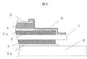
- FIG. The schematic cross section in the cross section A of FIG. The schematic diagram of the power module which shows the modification of Example 1.
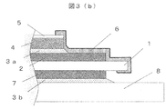
- FIG. The schematic diagram of the power module which shows the modification of Example 1.
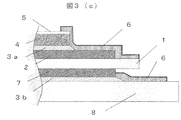
- FIG. The schematic diagram of the power module which shows the modification of Example 1.
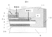
- FIG. 1 is a schematic cross-sectional view of a power module according to Embodiment 1.
- FIG. 5 is a cross-sectional SEM image in cross section B of FIG. 4. Sectional SEM image in the cross section C of FIG.
- FIG. 4 is a schematic cross-sectional view of a power module according to a second embodiment.
- FIG. 6 is a schematic plan view of a power module according to a fourth embodiment.
- FIG. 10 is a schematic diagram of a power module showing a modification of the fourth embodiment.
- FIG. 10 is a schematic diagram of a power module showing a modification of the fourth embodiment.
- 4 is a cross-sectional SEM image of a power module according to Example 4.
- FIG. 6 is a schematic plan view of a power module according to a fifth embodiment.
- FIG. 10 is a schematic cross-sectional view of a conventional power module.
- a conductor pattern 2 is formed on an insulating substrate 1
- a semiconductor chip 4 is connected to the conductor pattern 2 by a bonding member 3a
- a metal wire 9 is connected to an electrode 5 formed on the upper surface of the semiconductor chip 4. It is out.
- the ground electrode 7 formed on the back surface of the conductive pattern forming surface of the insulating substrate 1 is bonded to the metal heat sink 8 and the bonding member 3b.
- An insulating gel agent 11 is poured into the case 10 installed on the outer periphery of the heat sink 8 and sealed.
- Patent Documents 1 and 2 in order to suppress partial discharge, a method has been devised in which the end of the conductor pattern is covered with resin to improve the insulation characteristics.
- the partial discharge suppression effect varies greatly from product to product. Since the partial discharge suppression is insufficient only by coating with the resin, the insulation creepage distance must be set large in order to ensure the operational reliability of the power module. Therefore, the degree of freedom in module design is low, which is a factor that hinders downsizing of the module.
- FIG. 1 is a schematic plan view of a power module according to Embodiment 1 of the present invention
- FIG. 2 is a schematic cross-sectional view taken along a section A in FIG.
- the insulating substrate 1 is made of ceramics having excellent thermal conductivity for electrically insulating the heat sink 8 made of metal and the semiconductor chip 4.
- the conductor pattern 2 formed on the insulating substrate 1 is bonded to the semiconductor chip 4 by the bonding member 3a.
- Examples of the semiconductor chip 4 include power semiconductor chips such as IGBTs and control circuit semiconductor chips for controlling these power semiconductor chips.
- the ground electrode 7 is normally at a ground potential and is joined to the heat sink 8 by the joining member 3b.
- Examples of the joining members 3a and 3b include metals such as solder and silver, and silver paste obtained by adding silver to a resin.
- An electrode 5 is formed on the upper surface of the semiconductor chip 4 and a metal wire 9 is bonded thereto.
- the surface of the bonding member 3a, the conductor pattern 2, and the insulating substrate 1 including the electrode 5 formed on the upper surface of the semiconductor chip 4 and the outer peripheral end surface of the semiconductor chip 4 and continuing to the outer peripheral end surface of the semiconductor chip 4 is made of an inorganic material such as ceramics.
- the insulating film 6 is covered.
- the inorganic material used for the insulating film any conventionally known material can be used as long as it is electrically insulating.
- oxide ceramics such as aluminum oxide, or nitride ceramics such as aluminum nitride or silicon nitride can be used.
- Aluminum oxide is preferable in terms of insulating properties, handling in the air, and cost.
- the insulating film 6 only needs to include a part of the surface of the insulating substrate 1. When the insulating film 6 covers the end of the insulating substrate 1 as shown in FIG. As shown, the case where the insulating film 6 covers the surface of the insulating substrate facing the heat sink 8 is also included in this embodiment. Further, as shown in FIG. 3C, the insulating film 6 may cover a part of the ground electrode 7 and the heat radiating plate 8.
- the insulating film 6 may be divided into a plurality of films with respect to the semiconductor chip 4.
- FIG. 4 shows a schematic cross-sectional view.
- the configuration of this power module will be described.
- the insulating substrate 1 is a silicon nitride sintered substrate, and copper plates are bonded to both surfaces of the insulating substrate as a conductor pattern 2 and a ground electrode 7, respectively.
- An IGBT and a control circuit semiconductor chip for controlling the IGBT are arranged on the conductor pattern.
- These semiconductor chips 4 are connected to the conductor pattern 2 by high-temperature solder 3a.
- Aluminum electrodes 5 are formed on the upper surface of the semiconductor chip 4, and between the semiconductor chips 4 and between the semiconductor chip 4 and the conductor pattern 2 are connected by aluminum wires 9.
- the ground electrode 7 is connected to the copper heat sink 8 by a low temperature solder 3b.
- the surface of the bonding member 3a, the conductor pattern 2, and the insulating substrate 1 including the electrode 5 and the outer peripheral end surface of the semiconductor chip 4 and continuing to the outer peripheral end surface of the semiconductor chip 4 is covered with an insulating film 6 made of an inorganic material.
- the inorganic material aluminum oxide, which is an insulating ceramic, was used.
- the insulating film 6 was formed by an aerosol deposition method. Thereafter, the case 10 is adhered to the periphery of the heat radiating plate 8, filled with a silicon-based insulating gel agent 11 and cured, and then the upper portion is sealed to complete the module. *
- FIG. 1 An explanatory diagram of the configuration of the aerosol deposition apparatus is shown in FIG.
- the high-pressure gas cylinder 21 is opened, and the carrier gas is introduced into the aerosol generator 23 through the gas carrier pipe 22.
- the aerosol generator 23 contains aluminum oxide fine particles in advance and is mixed with a carrier gas to generate an aerosol containing aluminum oxide fine particles.
- Usable carrier gases include inert gases such as argon, nitrogen and helium.
- the operation of the vacuum pump 29 reduces the pressure in the vacuum chamber 25 to several hundred Pa.
- Aluminum oxide fine particles having an average particle diameter of 0.5 ⁇ m were used as the raw material powder, and nitrogen gas was flowed into the apparatus as a carrier gas at a flow rate of 3 to 15 L / min.
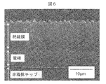
- FIGS. 6 and FIG. 7 show cross-sectional SEM images of the insulating film at the electrode end (section B in FIG. 4) and the conductor pattern end (section C in FIG. 4) of the produced power module.
- a dense film having no voids in the bonding interface with the base and in the film was formed.
- the film thickness of the insulating film shown in FIGS. 6 and 7 is about 10 ⁇ m, but the film thickness can be easily controlled by changing the film formation conditions.
- FIG. 8 shows the insulation characteristics of the power module in Example 1 in terms of dielectric breakdown voltage, and shows a result compared with that of a power module having a conventional structure in which the conductor pattern ends are covered with resin.
- the variation in breakdown voltage is large. This is because the resin pattern is not uniformly coated on the end portion of the conductor pattern, and the insulation characteristics vary from product to product.
- the insulation of the power module it is necessary to consider the minimum value of variation. As a result, in order to maintain a sufficient insulation characteristic, means such as increasing the insulation creepage distance is required.
- the dielectric breakdown voltage is larger than that of the conventional structure, and the variation is small.
- the power module in the present embodiment can be designed to reliably suppress partial discharge based on the insulating characteristics of the insulating film. Therefore, the operation reliability of the power module is improved as compared with the conventional structure, and the insulation specification can be satisfied with a small insulation creepage distance, so that the power module can be downsized.
- FIG. 9 is a schematic cross-sectional view of a power module according to the second embodiment.
- the insulating film 6 described in the first embodiment covers the surfaces of the plurality of electrically independent electrodes 5a and 5b formed on the upper surface of the semiconductor chip 4 and between the electrodes 5a and 5b. Except for this, the configuration is the same as in the first embodiment.
- Example 3 the inorganic material constituting the insulating film 6 described in Example 1 is composed of one kind of inorganic material or a composite of two or more kinds of inorganic materials, and the insulating film 6 has the thermal expansion of the conductor pattern 2.
- the configuration is the same as in Example 1 except that the coefficient of thermal expansion is smaller than the coefficient.
- the insulating film 6 is formed on a plurality of base materials such as the semiconductor chip 4, the conductor pattern 2, and the insulating substrate 1, and these base materials have different coefficients of thermal expansion.
- the thermal expansion coefficient of silicon used for semiconductor chips is about 3 ppm / ° C.
- the thermal expansion coefficient of copper used for conductor patterns is about 17 ppm / ° C.
- the thermal expansion coefficient of silicon nitride used for insulating substrates is about 3 ppm / ° C. It is.
- the semiconductor chip 4 repeats heat generation and cooling. Therefore, under such a thermal cycle, thermal stress corresponding to the difference in thermal expansion coefficient is generated at the interface between the insulating film 6 and the base material.
- thermal expansion coefficient of the insulating film 6 When the thermal expansion coefficients of the semiconductor chip 4, the conductor pattern 2, and the insulating substrate 1 are ⁇ c, ⁇ e, and ⁇ s, the thermal expansion coefficients generally have a magnitude relationship of ⁇ c, ⁇ s ⁇ e.
- the thermal expansion coefficient of the insulating film 6 is ⁇ i
- an inorganic material satisfying ⁇ c and ⁇ s ⁇ i ⁇ e is selected as the insulating film
- the difference in the thermal expansion coefficient between the insulating film 6 and each base material. Can be reduced evenly.
- silicon thermal expansion coefficient is about 3 ppm / ° C
- copper thermal expansion coefficient is about 17 ppm / ° C
- silicon nitride thermal expansion coefficient is about 3 ppm / ° C
- Aluminum oxide thermal expansion coefficient of about 7 ppm / ° C.
- aluminum nitride thermal expansion coefficient of about 5 ppm / ° C.
- the thermal expansion coefficient of the insulating film 6 is equal to the thermal expansion coefficient of the raw material powder used for film formation.
- an insulating film having a thermal expansion coefficient corresponding to the mixing ratio can be obtained. Therefore, an insulating film having an appropriate thermal expansion coefficient can be formed according to the conductor pattern used in the power module and the thermal expansion coefficient of the insulating substrate. Furthermore, the coefficient of thermal expansion of the insulating film can be changed according to the film formation location.
- the thermal expansion coefficient of the insulating film is close to the thermal expansion coefficient of the insulating substrate on the insulating substrate, and the thermal expansion coefficient of the conductive pattern on the conductive pattern. It is possible to form a film so as to be close to the thickness and effectively suppress thermal stress.
- FIG. 11 is a schematic plan view of a power module according to the fourth embodiment of the present invention
- FIGS. 12A and 12B are schematic cross-sectional views in a cross section D and a cross section E in FIG. 11, respectively.
- the same components as those in the first embodiment are denoted by the same reference numerals, and the description thereof is omitted.
- the insulating film 6 made of an inorganic material does not necessarily have to be an insulating film, and is therefore referred to as an inorganic film 60 and distinguished from the insulating film 6.
- the inorganic film 60 covers at least a part of the joint between the electrode 5 and the metal wire 9 formed on the upper surface of the semiconductor chip 4.
- the metal wire 9 connects the conductor pattern 2 and the electrode 5 and is connected to the semiconductor chip 4 via the electrode 5 on the semiconductor chip 4.
- the semiconductor chip 4 repeats heat generation and cooling. Therefore, under such a thermal cycle, a thermal stress corresponding to the difference in thermal expansion coefficient between the semiconductor chip 4 and the metal wire 9 is generated at the bonding interface between the electrode 5 and the metal wire 9. Cracks occur at the interface between the electrode 5 and the metal wire 9 due to thermal stress. As the driving time becomes longer, cracks develop and eventually the metal wire 9 is peeled off.
- thermosetting resin containing inorganic particles such as a thermosetting resin such as epoxy resin or polyimide resin or silica
- the above resin it is difficult to control the film thickness at the time of coating, and the metal wire joint cannot be coated uniformly with the resin.
- the non-uniform coating of the joint with a resin having a high coefficient of thermal expansion may promote peeling of the metal wire. For this reason, the reinforcing effect of the metal wire joint varies from product to product, and the operational reliability of the power module cannot be ensured.
- the inorganic film 60 made of an inorganic material such as ceramics covers at least a part of the surface of the metal wire 9 at the connection portion between the electrode 5 and the electrode 5 formed on the upper surface of the semiconductor chip 4. Take the structure.
- an inorganic material such as ceramics having a smaller coefficient of thermal expansion than the metal wire 9 the thermal expansion of the metal wire 9 at the time of high temperature is suppressed, and it acts on the bonding interface between the electrode 5 and the metal wire 9.
- Thermal stress can be reduced. Thereby, generation
- compressive stress can remain in the inorganic film 60 at room temperature during film formation.
- tensile stress remains in the electrode 5 and the semiconductor chip 4 on the substrate side of the inorganic film 60.
- the tensile stress applied to the semiconductor chip 4 at room temperature has the effect of reducing the thermal stress applied to the bonding member 3a at a high temperature. Thereby, it is effective in the fatigue reduction of the joining member 3a by a thermal cycle, and destruction of the power module resulting from the crack progress in the joining member 3a can also be suppressed.
- any material can be used as long as the coefficient of thermal expansion is smaller than that of the metal wire 9.
- examples thereof include oxide ceramics such as aluminum oxide, titanium oxide, and zirconium oxide, nitride ceramics such as aluminum nitride and silicon nitride, and carbide ceramics such as silicon carbide.
- the inorganic material which comprises an inorganic film does not need to be 1 type, and 2 or more types of inorganic materials may be mixed.
- the thermal expansion coefficient of the inorganic film is equal to the thermal expansion coefficient of the raw material powder used for film formation.
- a film having a thermal expansion coefficient corresponding to the mixing ratio can be obtained. Therefore, an inorganic film having an appropriate thermal expansion coefficient can be formed according to the thermal expansion coefficient of the metal wire or semiconductor chip used in the power module.
- the inorganic film 60 only needs to cover the electrode 5 on the semiconductor chip 4 and a part of the surface of the metal wire 9 at the junction with the electrode 5, as shown in FIGS. As shown in b), there may be a portion where no film is formed on the surface of the metal wire 9 and the surface of the electrode 5.
- Example 4 A method for manufacturing a power module in Example 4 will be described. Since the components of the power module other than the inorganic film 60 are the same as those in the first embodiment, description thereof is omitted.
- Aluminum oxide is selected as the constituent material of the inorganic film 60, and the inorganic film 60 is formed at least on the surface of the metal wire 9 at the connection portion between the electrode 5 formed on the upper surface of the semiconductor chip 4 and the electrode 5 by an aerosol deposition method. A film was formed so as to cover a part.
- aluminum oxide fine particles having an average particle diameter of 0.5 ⁇ m were used as a raw material powder, and nitrogen gas was flowed into the apparatus as a carrier gas at a flow rate of 3 to 15 L / min.
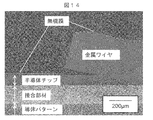
- FIG. 14 shows an SEM image at the metal wire joint of the manufactured power module.
- FIG. 15 shows an SEM image in which the bonding interface between the inorganic film, the underlying electrode, and the metal wire is enlarged. A dense film having no voids in the bonding interface with the base and in the film was formed.
- the film thickness of the aluminum oxide film shown in FIGS. 14 and 15 is about 20 ⁇ m, but the film thickness can be easily controlled by changing the film formation conditions.
- Residual stress acting on the aluminum oxide film and the semiconductor chip was examined by the X-ray sin2 ⁇ method. It was confirmed by the film formation that a compressive stress of about 50 to 200 MPa was applied to the aluminum oxide film and a tensile stress of about 0 to 200 MPa was applied to the semiconductor chip.
- the tensile stress applied to the semiconductor chip 4 at room temperature reduces the thermal stress applied to the solder at a high temperature, which is effective in reducing solder fatigue during power cycles and also suppresses the destruction of the power module due to the progress of solder cracks. be able to.
- the power module in this embodiment the electrode formed on the upper surface of the semiconductor chip and the surface of the metal wire in the connection portion with the electrode are covered with an inorganic film, and further, compressive stress is applied to the inorganic film, thereby operating the power module. Reliability can be improved.
- FIG. 16 is a schematic plan view of a power module according to Embodiment 5 of the present invention.
- the same components as those in the fourth embodiment are denoted by the same reference numerals, and the description thereof is omitted.
- an electrically insulating material is selected as the inorganic material, and the inorganic film 60 is collectively covered from the electrode 5 on the semiconductor chip 4 to the insulating substrate 1.
- any conventionally known material can be used as the inorganic material for the insulating film as long as it is electrically insulating.
- oxide ceramics such as aluminum oxide, or nitride ceramics such as aluminum nitride or silicon nitride can be used.
- Aluminum oxide is preferable in terms of insulating properties, handling in the air, and cost.
Landscapes
- Structures Or Materials For Encapsulating Or Coating Semiconductor Devices Or Solid State Devices (AREA)
- Cooling Or The Like Of Semiconductors Or Solid State Devices (AREA)
Abstract
効果的に部分放電を抑止できる絶縁膜を被覆することで、パワーモジュールの動作信頼性を向上させるとともに、絶縁沿面距離を小さくすることによるパワーモジュールの小型化が可能になる技術を提供する。 上記課題を解決するため、本発明は、絶縁基板と、前記絶縁基板上に形成された導体パターンと、前記導体パターンと接合部材により接続された半導体チップと、前記半導体チップ上面に形成された電極と、前記半導体チップ外周端面と、前記半導体チップ外周端面と連続する前記接合部材と、前記導体パターンと、前記絶縁基板の表面とを被覆し、無機材料からなる絶縁膜とを備えることを特徴とするパワーモジュールを提供する。
Description
本発明は、パワーモジュール及びその製造方法に関する。
特許文献1、特許文献2等には、絶縁基板に導体パターンを形成し、導体パターン上に半導体チップを接合部材で接続し、半導体チップ上面に形成された電極に電極と導体パターンとを接続する金属ワイヤを結んだパワーモジュールにおいて、例えば、エポキシ樹脂、フェノール樹脂、ポリイミド樹脂等の熱硬化性樹脂や上記熱硬化性樹脂にアルミナ、シリカ等の無機粒子を含有させた絶縁体を導体パターン端部に被覆する方法が記載されている。
パワーモジュールの動作信頼性を阻害する要因の一つにパワーモジュール内部での部分放電の発生がある。特許文献1、特許文献2では、部分放電を抑制するために、導体パターン端部を樹脂で被覆している。しかし、樹脂は被覆する際の膜厚制御が難しく、導体パターン端部に絶縁体を均一に被覆できないため、製品ごとで部分放電抑止効果が大きくばらつく。樹脂による被覆だけでは、部分放電抑止が不十分であるため、パワーモジュールの動作信頼性を確保するためには絶縁沿面距離を大きく設定せざるを得ない。そのため、モジュール設計の自由度が低く、モジュール小型化を阻害する要因になっている。
また、パワーモジュールの駆動時には、半導体チップが発熱と冷却を繰り返す。金属ワイヤと半導体チップとの熱望楼率の差に応じた熱応力が電極と金属ワイヤの接合部に発生し、電極と金属ワイヤの接合部において亀裂が進展し、剥離が生じる可能性があり、信頼性の向上が必要であった。
上記問題点に鑑み本発明では、効果的に部分放電を抑止できる絶縁膜を被覆することで、パワーモジュールの動作信頼性を向上させるとともに、絶縁沿面距離を小さくすることによるパワーモジュールの小型化が可能になる技術を提供することを目的とする。
また、他の観点における本発明では、電極と金属ワイヤの接合部を補強することで、動作の信頼性を確保する技術を提供することを目的とする。
上記課題を解決するため、本発明は、絶縁基板と、前記絶縁基板上に形成された導体パターンと、前記導体パターンと接合部材により接続された半導体チップと、前記半導体チップ上面に形成された電極と、前記電極と、前記半導体チップと、前記接合部材と、前記導体パターンと、前記絶縁基板の表面とを被覆し、無機材料からなる絶縁膜とを備えることを特徴とするパワーモジュールを提供する。
また、他の観点における本発明は、絶縁基板と、前記絶縁基板上に形成された導体パターンと、前記導体パターンと接合部材により接続された半導体チップと、前記半導体チップ上面に形成された電極と、前記電極と前記導体パターンとを接続する金属ワイヤと、前記金属ワイヤと前記電極の接合部の少なくとも一部を被覆する無機材料からなる無機膜とを備えることを特徴とするパワーモジュールを提供する。
本発明によれば、効果的に部分放電を抑止できる絶縁膜を被覆することで、パワーモジュールの動作信頼性が向上するとともに、絶縁沿面距離を小さくすることによるパワーモジュールの小型化が可能となる。
また、他の観点における本発明によれば、電極と金属ワイヤの接合部を補強することで、動作の信頼性を確保することができる。
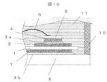
図10は、従来におけるパワーモジュールの模式断面図である。図10に示すように、絶縁基板1に導体パターン2を形成し、導体パターン2上に半導体チップ4を接合部材3aで接続し、半導体チップ4上面に形成された電極5に金属ワイヤ9を結んでいる。絶縁基板1の導体パターン形成面の裏面に形成された接地電極7は金属製の放熱板8と接合部材3bにより接合される。放熱板8の外周に設置されたケース10の内部に絶縁性ゲル剤11を流し込み封止している。
パワーモジュールの動作信頼性を阻害する要因の一つにパワーモジュール内部での部分放電の発生がある。動作時のパワーモジュールでは、導体パターン2や電極5と接地された放熱板8の間に数kVの電位差が存在するため、パワーモジュール内部の絶縁特性が不十分であると、導体パターンや電極と放熱板間に部分放電が発生する。パワーモジュール動作時に部分放電が発生するとパワーモジュールとしての性能が得られないだけでなく、部分放電を繰り返すことで絶縁破壊も招く。そのため、十分な絶縁特性を保証する設計を施すことで部分放電を抑止する必要がある。絶縁特性の向上を実現する手段としては、放熱板と導体パターン間、または導体パターン間の絶縁沿面距離を大きく設定することが一般的に知られている。
しかし、導体パターンや半導体チップに付着した金属異物、導体パターン形成時にできた絶縁基板上の金属残渣などの表面汚染が存在すると、動作電圧に対して絶縁沿面距離を十分に設定しても、表面汚染を経由して部分放電が発生する場合がある。
そこで、特許文献1、2に示すように部分放電を抑制するために、導体パターン端部を樹脂で被覆し絶縁特性を向上させる方法が考案されている。
しかし、樹脂は被覆する際の膜厚制御が難しく、導体パターン端部に絶縁体を均一に被覆できないため、製品ごとで部分放電抑止効果が大きくばらつく。樹脂による被覆だけでは、部分放電抑止が不十分であるため、パワーモジュールの動作信頼性を確保するためには絶縁沿面距離を大きく設定せざるを得ない。そのため、モジュール設計の自由度が低く、モジュール小型化を阻害する要因になっている。
以下、そこで、上記問題点に鑑みなされた本発明に係る各実施例について、図面を用いて説明する。
図1は本発明の実施例1におけるパワーモジュールの模式平面図であり、図2は図1の断面Aにおける模式断面図である。絶縁基板1は金属からなる放熱板8と半導体チップ4を電気的に絶縁するための熱伝導性に優れたセラミックスからなる。絶縁基板1に形成された導体パターン2は半導体チップ4と接合部材3aにより接合される。半導体チップ4としては、IGBTなどのパワー半導体チップやこれらのパワー半導体チップを制御するための制御回路用半導体チップが挙げられる。接地電極7は、通常接地電位であり、放熱板8と接合部材3bで接合される。接合部材3a、3bとしては、はんだや銀などの金属、及び樹脂に銀を加えた銀ペーストなどが挙げられる。半導体チップ4上面には、電極5が形成されており、金属ワイヤ9が接合される。そして、半導体チップ4上面に形成された電極5、及び半導体チップ4外周端面を含み、半導体チップ4外周端面と連続する接合部材3a、導体パターン2、絶縁基板1の表面をセラミックスなどの無機材料からなる絶縁膜6で被覆する。絶縁膜に使用する無機材料としては、電気的に絶縁性であれば、従来公知のいずれの材料も使用できる。例えば、酸化アルミニウム等の酸化物系セラミックス、または窒化アルミニウムや窒化珪素等の窒化物系セラミックス等が挙げられるが、絶縁特性、大気中での取り扱い、及びコストの点において、酸化アルミニウムが望ましい。絶縁膜6は、絶縁基板1の表面の一部を含んでいれば良く、図3(a)に示すように絶縁膜6が絶縁基板1の端部まで被覆する場合、図3(b)に示すように絶縁膜6が放熱板8と対向する絶縁基板表面まで被覆する場合も本実施例に含まれる。また、図3(c)に示すように、絶縁膜6が接地電極7や放熱板8の一部を被覆していても良い。部分放電は電極5または導体パターン2から接地電位に向かって生じるため、接地電位である接地電極7や放熱板8を被覆することで、部分放電の抑制効果がさらに得られる。本発明は、絶縁膜6が半導体チップ4の外周端部を全て被覆する必要はなく、絶縁膜6が半導体チップ4の外周端部の一部のみを被覆していても、表面汚染に起因する部分放電の抑止効果がある。また、図3(d)のように、絶縁膜6を半導体チップ4に対して複数に分割して成膜しても良い。
半導体チップ上面の電極から、絶縁基板までを無機材料の絶縁膜により一括して被覆することで、部分放電発生箇所である電極端部、及び導体パターン端部を同時に被覆し、部分放電を効果的に抑止できる。さらに、従来の構造に比べ広い領域に膜厚が制御された絶縁膜を被覆することで、付着金属異物や金属残渣などの表面汚染に起因する部分放電に対しても十分な絶縁特性を保つことができる。絶縁膜の膜厚制御が容易であるため、絶縁膜の絶縁特性をもとに部分放電を確実に抑制する設計が可能になる。したがって、従来の構造よりも小さな絶縁沿面距離で絶縁仕様を満足できるようになり、パワーモジュールの小型化が可能となる。
ここで、実施例1におけるパワーモジュールを製造方法について説明する。図4に模式断面図を示す。このパワーモジュールの構成について説明する。絶縁基板1は窒化シリコン焼結基板であり、絶縁基板の両面にはそれぞれ銅板が導体パターン2及び接地電極7として接合されている。導体パターン上にはIGBT、及びIGBTを制御するための制御回路用半導体チップが配置されている。これらの半導体チップ4は高温はんだ3aにより導体パターン2に接続される。半導体チップ4上面にはアルミ電極5が形成されており、半導体チップ4間および、半導体チップ4と導体パターン2がアルミワイヤ9により結線される。接地電極7は銅の放熱板8と低温はんだ3bにより接続される。そして、電極5、及び半導体チップ4外周端面を含み、半導体チップ4外周端面と連続する接合部材3a、導体パターン2、絶縁基板1の表面を無機材料の絶縁膜6で被覆する。無機材料として、絶縁性セラミックスである酸化アルミニウムを使用した。絶縁膜6はエアロゾルデポジション法により成膜した。その後、放熱板8の周囲にケース10を接着させ、シリコン系の絶縁性ゲル剤11を充填して硬化させた後、上部を封止してモジュールを完成させる。
次に、エアロゾルデポジション法による成膜方法を説明する。エアロゾルデポジション装置の構成説明図を図5に示す。高圧ガスボンベ21を開栓し、搬送ガスをガス搬送管22を通してエアロゾル発生器23に導入させる。エアロゾル発生器23にはあらかじめ酸化アルミニウムの微粒子を入れており、搬送ガスと混合されることで、酸化アルミニウム微粒子を含むエアロゾルが発生する。使用可能な搬送ガスとしては、アルゴン、窒素、ヘリウム等の不活性ガスが挙げられる。エアロゾルは、搬送管24を通してノズル26へと送られ、XYステージ27に設置された基板28に向けてノズルの開口より高速で噴出される。このとき真空ポンプ29の作動により、真空チャンバー25内は数100Paの減圧となる。原料粉末として平均粒径0.5μmの酸化アルミニウム微粒子を使用し、搬送ガスとして窒素ガスを3~15L/minの流量で装置内に流した。
作製したパワーモジュールの電極端部(図4の断面B)、及び導体パターン端部(図4の断面C)での絶縁膜の断面SEM画像を図6、図7にそれぞれ示す。下地との接合界面、及び膜中にボイドのない緻密な膜が成膜された。図6、図7に示す絶縁膜の膜厚は約10μmであるが、膜厚は成膜条件を変えることで容易に制御可能である。
図8は実施例1におけるパワーモジュールの絶縁特性を絶縁破壊電圧で示し、導体パターン端部を樹脂で被覆した従来構造のパワーモジュールのそれと比較した結果を示している。従来構造の場合、絶縁破壊電圧のばらつきが大きい。これは導体パターン端部に樹脂が均一に被覆されておらず、製品ごとにその絶縁特性がばらつくためである。パワーモジュールの絶縁設計をするうえでは、ばらつきの最低値を考慮しなければならず、結果として十分な絶縁特性を保持させるためには、絶縁沿面距離を大きくするなどの手段が必要となる。一方、本実施例の構造では、絶縁破壊電圧が従来構造に比べ大きいうえ、そのばらつきも小さい。これは、半導体チップ上面の電極から、絶縁基板までを絶縁膜で一括して被覆することで、部分放電発生箇所である電極端部、及び導体パターン端部を同時に被覆しできるうえ、従来の構造に比べ広い領域に絶縁膜を被覆することで、付着金属異物や金属残渣などの表面汚染に起因する放電に対しても十分な絶縁特性をもつためである。また、絶縁膜の膜厚制御が容易であり、均一な絶縁膜を被覆できるため、絶縁破壊電圧のばらつきも小さい。本実施例におけるパワーモジュールでは、絶縁膜の絶縁特性をもとに部分放電を確実に抑制する設計が可能になる。したがって、従来の構造に比べパワーモジュールの動作信頼性が向上するとともに、小さな絶縁沿面距離で絶縁仕様を満足できるようになるため、パワーモジュールの小型化が可能となる。
図9を用いて、本発明の実施例2を説明する。本実施例では実施例1と同一の構成要素に同一の符号を付し、その説明を省略するものとする。図9は実施例2におけるパワーモジュールの模式断面図である。実施例2においては、実施例1に記載の絶縁膜6が、半導体チップ4上面に形成された電気的に独立した複数の電極5a、5bの表面、及び電極5aと電極5bの間を被覆していること以外は実施例1と同様に構成される。
半導体チップ4上面に電気的に独立した複数の電極5a、5bが形成されている場合、電極間に十分な絶縁を保障する距離をとらなければならない。半導体チップ上の電極間を無機材料からなる絶縁膜で被覆することで、電極間の絶縁強化が可能になる。膜厚が制御された絶縁膜を被覆することで、十分な絶縁特性を確保できる設計が可能になるため、従来構造よりも電極間の距離を小さく設定できる。これにより、電極パターンの微細化、さらにはモジュールの小型化が可能となる。
実施例3においては、実施例1に記載の絶縁膜6を構成する無機材料が1種類の無機材料又は2種類以上の無機材料の複合物からなり、上記絶縁膜6が導体パターン2の熱膨張率より小さい値の熱膨張率を有すること以外は実施例1と同様に構成される。
絶縁膜6は半導体チップ4、導体パターン2、絶縁基板1などの複数の基材に成膜されており、これらの基材はそれぞれ熱膨張率が異なる。例えば、半導体チップに使われる珪素の熱膨張率は3ppm/℃程度、導体パターンに使われる銅の熱膨張率は17ppm/℃程度、絶縁基板に使われる窒化珪素の熱膨張率は3ppm/℃程度である。パワーモジュールの駆動時は、半導体チップ4が発熱、冷却を繰り返す。したがって、このような熱サイクルの下では、絶縁膜6と基材間の界面に熱膨張率の差に応じた熱応力が発生する。この熱応力は、絶縁膜の剥離や、絶縁膜中の欠陥導入による部分放電抑制効果の低下を引き起こす可能性がある。そこで、絶縁膜6の熱膨張率を基材に近づけ、絶縁膜6と基材との界面に働く熱応力を最小限に抑える必要がある。半導体チップ4、導体パターン2、絶縁基板1の熱膨張率をαc、αe、αsとすると、一般に熱膨張率にはαc、αs<αeの大小関係がある。したがって、絶縁膜6の熱膨張率をαiとしたとき、αc、αs<αi<αeとなるような無機材料を絶縁膜として選択すれば、絶縁膜6と各基材間の熱膨張率の差を均等に低減することができる。例えば、半導体チップに珪素(熱膨張率は3ppm/℃程度)、導体パターンに銅(熱膨張率17ppm/℃程度)、絶縁基板に窒化珪素(熱膨張率3ppm/℃程度)を使用した場合、酸化アルミニウム(熱膨張率7ppm/℃程度)、窒化アルミニウム(熱膨張率5ppm/℃程度)等が絶縁膜として適している。
絶縁膜6の熱膨張率は、成膜に用いる原料粉末の熱膨張率と等しい。熱膨張率が異なる2種類以上の無機材料の混合粉末を原料粉末に用いることにより、その混合比に応じた熱膨張率を有する絶縁膜が得られる。そのため、パワーモジュールに使われる導体パターンや絶縁基板の熱膨張率に応じて、適切な熱膨張率をもつ絶縁膜を形成することができる。さらに、成膜箇所に応じて、絶縁膜の熱膨張率を変化させることも可能である。つまり、原料粉末の混合比を変化させながら絶縁膜を成膜することで、絶縁膜の熱膨張率が絶縁基板上では絶縁基板の熱膨張率に近く、導体パターン上では導体パターンの熱膨張率に近くなるように成膜でき、熱応力を効果的に抑制できる。
図11は本発明の実施例4におけるパワーモジュールの模式平面図であり、図12(a)、(b)はそれぞれ図11の断面D、断面Eにおける模式断面図である。本実施例では実施例1と同一の構成要素に同一の符号を付し、その説明を省略するものとする。ただし、本実施例においては無機材料からなる絶縁膜6は必ずしも絶縁性をもつ膜である必要はないため、無機膜60と表記し、絶縁膜6と区別する。実施例4においては、無機膜60が、半導体チップ4上面に形成された電極5と金属ワイヤ9の接合部の少なくとも一部を被覆している。
パワーモジュールの動作信頼性を阻害する要因の一つに熱サイクルに伴う金属ワイヤの剥離がある。金属ワイヤ9は、導体パターン2と電極5とを接続するもので、半導体チップ4と半導体チップ4上の電極5を介して接続されている。パワーモジュールの駆動時は、半導体チップ4が発熱、冷却を繰り返す。したがって、このような熱サイクルの下では、半導体チップ4と金属ワイヤ9の熱膨張率の差に応じた熱応力が電極5と金属ワイヤ9の接合界面に発生する。熱応力により、電極5と金属ワイヤ9の界面部分で亀裂が発生する。駆動時間が長くなると亀裂が進展し最終的には金属ワイヤ9の剥離が生じる。パワーモジュールの動作安定性を確保するためには、部分放電の抑制とともに、金属ワイヤ9の剥離を防ぐ必要がある。金属ワイヤ接合部の補強として、エポキシ樹脂、ポリイミド樹脂等の熱硬化性樹脂やシリカ等の無機粒子を含有させた上記熱硬化性樹脂で金属ワイヤ接合部を補強する方法が考案されている。しかし、上記樹脂では被覆する際の膜厚制御が難しく、金属ワイヤ接合部に樹脂を均一に被覆できない。熱膨張率が大きい樹脂による接合部の不均一な被覆は、金属ワイヤの剥離を促すこともある。そのため、製品ごとで金属ワイヤ接合部の補強効果がばらつき、パワーモジュールの動作信頼性を確保できない。
そこで、実施例4においては、セラミックスなどの無機材料からなる無機膜60が、半導体チップ4上面に形成された電極5及び電極5との接続部における金属ワイヤ9の表面の少なくとも一部を被覆している構造をとる。金属ワイヤ9より熱膨張率の小さいセラミックスなどの無機材料で接続部の金属ワイヤ表面を被覆することで、高温時の金属ワイヤ9の熱膨張を抑え、電極5と金属ワイヤ9の接合界面にはたらく熱応力を低減することができる。これにより、接合界面の亀裂の発生、及び亀裂の進展を抑制することができ、金属ワイヤの剥離に起因するパワーモジュールの破壊を抑制することができる。
さらに、成膜時に室温において無機膜60に圧縮応力を残留させることが可能である。このとき、無機膜60の基板側となる電極5と半導体チップ4には引張応力が残留する。室温において半導体チップ4に加わる引張応力は、高温時に接合部材3aに加わる熱応力を低減する効果がある。これにより、熱サイクルによる接合部材3aの疲労低減に効果があり、接合部材3a内のクラック進展に起因するパワーモジュールの破壊も抑制することができる。
無機膜60に使用する無機材料としては、金属ワイヤ9より熱膨張率が小さければ、いずれの材料も使用できる。例えば、酸化アルミニウム、酸化チタン、酸化ジルコニウム等の酸化物系セラミックス、または窒化アルミニウムや窒化珪素等の窒化物系セラミックス、または炭化珪素等の炭化物系セラミックス等が挙げられる。また、無機膜を構成する無機材料は1種類である必要は無く、2種類以上の無機材料が混在していても良い。無機膜の熱膨張率は、成膜に用いる原料粉末の熱膨張率と等しい。熱膨張率が異なる2種類以上の無機材料の混合粉末を原料粉末に用いることにより、その混合比に応じた熱膨張率を有する膜が得られる。そのため、パワーモジュールに使われる金属ワイヤや半導体チップの熱膨張率に応じて、適切な熱膨張率をもつ無機膜を形成することができる。
本実施例によるパワーモジュールでは、無機膜60が半導体チップ4上の電極5、及び電極5との接合部における金属ワイヤ9表面の一部を被覆していれば良く、図13(a)、(b)に示すように、金属ワイヤ9表面、及び電極5表面に膜が成膜されていない箇所があっても良い。
実施例4におけるパワーモジュールの作製方法を説明する。無機膜60以外のパワーモジュールの構成要素は実施例1と同じであるため、説明を省略する。無機膜60の構成材料として、酸化アルミニウムを選択し、エアロゾルデポジション法により、無機膜60が、半導体チップ4上面に形成された電極5及び電極5との接続部における金属ワイヤ9の表面の少なくとも一部を被覆するように成膜した。エアロゾルデポジション法による成膜では、原料粉末として平均粒径0.5μmの酸化アルミニウム微粒子を使用し、搬送ガスとして窒素ガスを3~15L/minの流量で装置内に流した。
作製したパワーモジュールの金属ワイヤ接合部におけるSEM画像を図14に示す。また無機膜と下地の電極、及び金属ワイヤの接合界面を拡大したSEM画像を図15に示す。下地との接合界面、及び膜中にボイドのない緻密な膜が成膜された。図14、図15に示す酸化アルミニウム膜の膜厚は約20μmであるが、膜厚は成膜条件を変えることで容易に制御可能である。
酸化アルミニウム膜および半導体チップにはたらく残留応力をX線のsin2Ψ法により調べた。成膜により、酸化アルミニウム膜には50~200MPa程度の圧縮応力、半導体チップには0~200MPa程度の引張応力が付与されていることを確認した。室温において半導体チップ4に加わる引張応力は、高温時にはんだに加わる熱応力を低減するため、パワーサイクル時のはんだ疲労の低減に効果があり、はんだのクラック進展に起因するパワーモジュールの破壊も抑制することができる。
以上の構成でパワーサイクル試験を行った結果、ジャンクション温度50~150℃では、40000サイクルでもパワーモジュールが破壊されないことを確認した。一方、金属ワイヤ接合部の補強として、樹脂を用いた従来構造では、パワーサイクルの寿命が40000サイクルに到達しない。これは、樹脂では被覆する際の、膜厚制御が難しく、熱膨張率が大きい樹脂による接合部の不均一な被覆が金属ワイヤの剥離を促すためである。本実施例におけるパワーモジュールでは、半導体チップ上面に形成された電極及び電極との接続部における金属ワイヤの表面を無機膜により被覆し、さらに無機膜に圧縮応力を付与することで、パワーモジュールの動作信頼性を向上させることができる。
図16は本発明の実施例5におけるパワーモジュールの模式平面図である。本実施例では実施例4と同一の構成要素に同一の符号を付し、その説明を省略するものとする。本実施例においては、無機材料として電気的に絶縁性の材料を選択し、無機膜60を半導体チップ4上の電極5から、絶縁基板1までを一括して被覆することを特徴とする。
無機材料に絶縁性の材料を選択することで、実施例5に記載したパワーサイクル特性の向上だけでなく、実施例4に記載したパワーモジュールの絶縁特性の向上、及びパワーモジュールの小型化も可能となる。その際、絶縁膜に使用する無機材料としては、電気的に絶縁性であれば、従来公知のいずれの材料も使用できる。例えば、酸化アルミニウム等の酸化物系セラミックス、または窒化アルミニウムや窒化珪素等の窒化物系セラミックス等が挙げられるが、絶縁特性、大気中での取り扱い、及びコストの点において、酸化アルミニウムが望ましい。
これまで説明してきた実施例は、何れも本発明を実施するにあたっての具体化の一例を示したものに過ぎず、これらによって本発明の技術的範囲が限定的に解釈されない。すなわち、本発明はその技術思想、又はその主要な特徴から逸脱することなく、様々な形で実施することができる。
1 絶縁基板
2 導体パターン
3a、3b 接合部材
4 半導体チップ
5、5a、5b 電極
6 絶縁膜
7 接地電極
8 放熱板
9 金属ワイヤ
10 ケース
11 絶縁性ゲル剤
21 高圧ガスボンベ
22、24 搬送管
23 エアロゾル発生器
25 真空チャンバー
26 ノズル
27 XYステージ
28 基板
29 真空ポンプ
60 無機膜
2 導体パターン
3a、3b 接合部材
4 半導体チップ
5、5a、5b 電極
6 絶縁膜
7 接地電極
8 放熱板
9 金属ワイヤ
10 ケース
11 絶縁性ゲル剤
21 高圧ガスボンベ
22、24 搬送管
23 エアロゾル発生器
25 真空チャンバー
26 ノズル
27 XYステージ
28 基板
29 真空ポンプ
60 無機膜
Claims (11)
- 絶縁基板と、
前記絶縁基板上に形成された導体パターンと、
前記導体パターンと接合部材により接続された半導体チップと、
前記半導体チップ上面に形成された電極と、
前記電極と、前記半導体チップと、前記接合部材と、前記導体パターンと、前記絶縁基
板の表面とを被覆し、無機材料からなる絶縁膜とを備えることを特徴とするパワーモジュ
ール。 - 前記絶縁基板の前記導体パターンが形成された面と反対側の面に形成された接地電極と
、前記接地電極上に形成された放熱板を備え、前記接地電極と前記放熱板を無機材料から
なる絶縁膜で被覆することを特徴とする請求項1に記載のパワーモジュール。 - 前記電極は電気的に独立した複数の電極より形成され、前記絶縁膜が半導体チップ上に
形成された電気的に独立した複数の電極の表面及び前記電極間を被覆することを特徴とす
る請求項1または2のいずれかに記載のパワーモジュール。 - 前記絶縁膜が、酸化アルミニウムから構成されることを特徴とする請求項1乃至3のい
ずれかに記載のパワーモジュール。 - 前記絶縁膜を構成する無機材料が1種類の無機材料又は2種類以上の無機材料の複合物
からなり、前記絶縁膜が前記導体パターンの熱膨張率より小さい値の熱膨張率を有するこ
とを特徴とする請求項1乃至4のいずれかに記載のパワーモジュール。 - 前記絶縁膜がエアロゾルデポジション法に代表される粒子衝突成膜法により形成される
ことを特徴とする請求項1乃至5のいずれかに記載のパワーモジュールの製造方法。 - 絶縁基板と、
前記絶縁基板上に形成された導体パターンと、
前記導体パターンと接合部材により接続された半導体チップと、
前記半導体チップ上面に形成された電極と、
前記電極と前記導体パターンとを接続する金属ワイヤと、
前記金属ワイヤと前記電極の接合部の少なくとも一部を被覆する無機材料からなる無機
膜とを備えることを特徴とするパワーモジュール。 - 前記無機膜を構成する無機材料が絶縁性の材料からなり、前記半導体チップ外周端面と
、前記半導体チップ外周端面と連続する前記接合部材と、前記導体パターンと、前記絶縁
基板の表面とを被覆することを特徴とする請求項7に記載のパワーモジュール。 - 前記無機膜を構成する無機材料が1種類の無機材料又は2種類以上の無機材料の複合物
からなり、前記無機膜が前記金属ワイヤの熱膨張率より小さい値の熱膨張率を有すること
を特徴とする請求項7または8に記載のパワーモジュール。 - 前記無機膜に圧縮応力が残留することを特徴とする請求項7乃至9のいずれかに記載の
パワーモジュール。 - 前記無機膜がエアロゾルデポジション法に代表される粒子衝突成膜法により形成される
ことを特徴とする請求項7乃至10のいずれかに記載のパワーモジュールの製造方法。
Applications Claiming Priority (4)
| Application Number | Priority Date | Filing Date | Title |
|---|---|---|---|
| JP2010-205054 | 2010-09-14 | ||
| JP2010205054 | 2010-09-14 | ||
| JP2011034100A JP5759744B2 (ja) | 2010-09-14 | 2011-02-21 | パワーモジュール及びその製造方法 |
| JP2011-034100 | 2011-02-21 |
Publications (1)
| Publication Number | Publication Date |
|---|---|
| WO2012035680A1 true WO2012035680A1 (ja) | 2012-03-22 |
Family
ID=45831176
Family Applications (1)
| Application Number | Title | Priority Date | Filing Date |
|---|---|---|---|
| PCT/JP2011/002346 Ceased WO2012035680A1 (ja) | 2010-09-14 | 2011-04-22 | パワーモジュール及びその製造方法 |
Country Status (2)
| Country | Link |
|---|---|
| JP (1) | JP5759744B2 (ja) |
| WO (1) | WO2012035680A1 (ja) |
Cited By (1)
| Publication number | Priority date | Publication date | Assignee | Title |
|---|---|---|---|---|
| WO2014139519A3 (de) * | 2013-03-14 | 2015-01-15 | Rogers Germany Gmbh | Metall-keramik-substrat sowie verfahren zum herstellen eines metall-keramik-substrates |
Families Citing this family (6)
| Publication number | Priority date | Publication date | Assignee | Title |
|---|---|---|---|---|
| JP5921723B2 (ja) * | 2013-01-11 | 2016-05-24 | 三菱電機株式会社 | 半導体装置 |
| CN106463394B (zh) | 2014-04-28 | 2019-06-18 | 三菱电机株式会社 | 半导体装置 |
| JP6398398B2 (ja) * | 2014-07-09 | 2018-10-03 | 日産自動車株式会社 | 半導体装置 |
| JP6527419B2 (ja) * | 2015-07-31 | 2019-06-05 | 富士電機株式会社 | 電子デバイス |
| JP6891075B2 (ja) * | 2017-08-30 | 2021-06-18 | 株式会社 日立パワーデバイス | パワー半導体モジュール |
| WO2024095813A1 (ja) * | 2022-10-31 | 2024-05-10 | 日本発條株式会社 | 部品実装基板、部品実装基板の製造方法、電子モジュール、及び電子モジュールの製造方法 |
Citations (3)
| Publication number | Priority date | Publication date | Assignee | Title |
|---|---|---|---|---|
| JP2002076197A (ja) * | 2000-08-24 | 2002-03-15 | Toshiba Corp | 半導体装置用基板及び半導体装置 |
| JP2009302526A (ja) * | 2008-05-16 | 2009-12-24 | Denso Corp | 電子回路装置及びその製造方法 |
| JP2010157695A (ja) * | 2008-12-29 | 2010-07-15 | Jin Imu Myun | チップパッケージ化における保護薄膜コーティング |
Family Cites Families (1)
| Publication number | Priority date | Publication date | Assignee | Title |
|---|---|---|---|---|
| JP2009005983A (ja) * | 2007-06-28 | 2009-01-15 | Aruze Corp | 遊技機 |
-
2011
- 2011-02-21 JP JP2011034100A patent/JP5759744B2/ja not_active Expired - Fee Related
- 2011-04-22 WO PCT/JP2011/002346 patent/WO2012035680A1/ja not_active Ceased
Patent Citations (3)
| Publication number | Priority date | Publication date | Assignee | Title |
|---|---|---|---|---|
| JP2002076197A (ja) * | 2000-08-24 | 2002-03-15 | Toshiba Corp | 半導体装置用基板及び半導体装置 |
| JP2009302526A (ja) * | 2008-05-16 | 2009-12-24 | Denso Corp | 電子回路装置及びその製造方法 |
| JP2010157695A (ja) * | 2008-12-29 | 2010-07-15 | Jin Imu Myun | チップパッケージ化における保護薄膜コーティング |
Cited By (1)
| Publication number | Priority date | Publication date | Assignee | Title |
|---|---|---|---|---|
| WO2014139519A3 (de) * | 2013-03-14 | 2015-01-15 | Rogers Germany Gmbh | Metall-keramik-substrat sowie verfahren zum herstellen eines metall-keramik-substrates |
Also Published As
| Publication number | Publication date |
|---|---|
| JP2012084835A (ja) | 2012-04-26 |
| JP5759744B2 (ja) | 2015-08-05 |
Similar Documents
| Publication | Publication Date | Title |
|---|---|---|
| JP5759744B2 (ja) | パワーモジュール及びその製造方法 | |
| US11594475B2 (en) | Method of fabricating an electronic power module by additive manufacturing, and associated substrate and module | |
| CN1143382C (zh) | 绝缘衬底、其制作方法及具有绝缘衬底的模块半导体器件 | |
| CN105229785B (zh) | 功率半导体模块及其制造方法、电力变换器 | |
| CN103635997B (zh) | 用于制造结构化的烧结连接层的方法以及具有结构化的烧结连接层的半导体器件 | |
| JP2016012741A (ja) | 半導体装置およびその形成方法 | |
| WO2015151644A1 (ja) | 電力変換装置 | |
| CN104051397B (zh) | 包括非整数引线间距的封装器件及其制造方法 | |
| WO2016158110A1 (ja) | 静電チャック装置 | |
| CN105575936B (zh) | 制造电路载体方法及制造和运行半导体装置的方法 | |
| CN113206048A (zh) | 半导体装置及其制造方法 | |
| KR101331669B1 (ko) | 전력 모듈용 기판 | |
| JP6150718B2 (ja) | 半導体装置およびその製造方法 | |
| CN110178214A (zh) | 模块 | |
| JP5954374B2 (ja) | 絶縁基板、その製造方法、半導体モジュールおよび半導体装置 | |
| JP6399906B2 (ja) | パワーモジュール | |
| CN114078790A (zh) | 功率半导体模块装置及其制造方法 | |
| CN111727502A (zh) | 高频模块 | |
| US20190358285A1 (en) | A method of fabricating an electronic power module by additive manufacturing, and associated substrate and module | |
| WO2013105351A1 (ja) | パワーモジュール | |
| JP5868187B2 (ja) | 電子回路基板及び半導体装置 | |
| US10403566B2 (en) | Power module | |
| Schulz-Harder | Advanced DBC (direct bonded copper) substrates for high power and high voltage electronics | |
| CN111834307B (zh) | 半导体模块 | |
| WO2015170488A1 (ja) | 半導体装置及びその製造方法 |
Legal Events
| Date | Code | Title | Description |
|---|---|---|---|
| 121 | Ep: the epo has been informed by wipo that ep was designated in this application |
Ref document number: 11824700 Country of ref document: EP Kind code of ref document: A1 |
|
| NENP | Non-entry into the national phase |
Ref country code: DE |
|
| 122 | Ep: pct application non-entry in european phase |
Ref document number: 11824700 Country of ref document: EP Kind code of ref document: A1 |