WO2012017565A1 - レーザリフトオフ装置 - Google Patents
レーザリフトオフ装置 Download PDFInfo
- Publication number
- WO2012017565A1 WO2012017565A1 PCT/JP2010/066793 JP2010066793W WO2012017565A1 WO 2012017565 A1 WO2012017565 A1 WO 2012017565A1 JP 2010066793 W JP2010066793 W JP 2010066793W WO 2012017565 A1 WO2012017565 A1 WO 2012017565A1
- Authority
- WO
- WIPO (PCT)
- Prior art keywords
- laser
- workpiece
- laser beam
- irradiation
- substrate
- Prior art date
- Legal status (The legal status is an assumption and is not a legal conclusion. Google has not performed a legal analysis and makes no representation as to the accuracy of the status listed.)
- Ceased
Links
Images







Classifications
-
- H—ELECTRICITY
- H10—SEMICONDUCTOR DEVICES; ELECTRIC SOLID-STATE DEVICES NOT OTHERWISE PROVIDED FOR
- H10H—INORGANIC LIGHT-EMITTING SEMICONDUCTOR DEVICES HAVING POTENTIAL BARRIERS
- H10H20/00—Individual inorganic light-emitting semiconductor devices having potential barriers, e.g. light-emitting diodes [LED]
- H10H20/80—Constructional details
-
- B—PERFORMING OPERATIONS; TRANSPORTING
- B23—MACHINE TOOLS; METAL-WORKING NOT OTHERWISE PROVIDED FOR
- B23K—SOLDERING OR UNSOLDERING; WELDING; CLADDING OR PLATING BY SOLDERING OR WELDING; CUTTING BY APPLYING HEAT LOCALLY, e.g. FLAME CUTTING; WORKING BY LASER BEAM
- B23K26/00—Working by laser beam, e.g. welding, cutting or boring
- B23K26/50—Working by transmitting the laser beam through or within the workpiece
-
- B—PERFORMING OPERATIONS; TRANSPORTING
- B23—MACHINE TOOLS; METAL-WORKING NOT OTHERWISE PROVIDED FOR
- B23K—SOLDERING OR UNSOLDERING; WELDING; CLADDING OR PLATING BY SOLDERING OR WELDING; CUTTING BY APPLYING HEAT LOCALLY, e.g. FLAME CUTTING; WORKING BY LASER BEAM
- B23K26/00—Working by laser beam, e.g. welding, cutting or boring
- B23K26/02—Positioning or observing the workpiece, e.g. with respect to the point of impact; Aligning, aiming or focusing the laser beam
- B23K26/06—Shaping the laser beam, e.g. by masks or multi-focusing
- B23K26/064—Shaping the laser beam, e.g. by masks or multi-focusing by means of optical elements, e.g. lenses, mirrors or prisms
- B23K26/066—Shaping the laser beam, e.g. by masks or multi-focusing by means of optical elements, e.g. lenses, mirrors or prisms by using masks
-
- B—PERFORMING OPERATIONS; TRANSPORTING
- B23—MACHINE TOOLS; METAL-WORKING NOT OTHERWISE PROVIDED FOR
- B23K—SOLDERING OR UNSOLDERING; WELDING; CLADDING OR PLATING BY SOLDERING OR WELDING; CUTTING BY APPLYING HEAT LOCALLY, e.g. FLAME CUTTING; WORKING BY LASER BEAM
- B23K26/00—Working by laser beam, e.g. welding, cutting or boring
- B23K26/02—Positioning or observing the workpiece, e.g. with respect to the point of impact; Aligning, aiming or focusing the laser beam
- B23K26/06—Shaping the laser beam, e.g. by masks or multi-focusing
- B23K26/067—Dividing the beam into multiple beams, e.g. multi-focusing
- B23K26/0676—Dividing the beam into multiple beams, e.g. multi-focusing into dependently operating sub-beams, e.g. an array of spots with fixed spatial relationship or for performing simultaneously identical operations
-
- B—PERFORMING OPERATIONS; TRANSPORTING
- B23—MACHINE TOOLS; METAL-WORKING NOT OTHERWISE PROVIDED FOR
- B23K—SOLDERING OR UNSOLDERING; WELDING; CLADDING OR PLATING BY SOLDERING OR WELDING; CUTTING BY APPLYING HEAT LOCALLY, e.g. FLAME CUTTING; WORKING BY LASER BEAM
- B23K26/00—Working by laser beam, e.g. welding, cutting or boring
- B23K26/36—Removing material
- B23K26/40—Removing material taking account of the properties of the material involved
-
- B—PERFORMING OPERATIONS; TRANSPORTING
- B23—MACHINE TOOLS; METAL-WORKING NOT OTHERWISE PROVIDED FOR
- B23K—SOLDERING OR UNSOLDERING; WELDING; CLADDING OR PLATING BY SOLDERING OR WELDING; CUTTING BY APPLYING HEAT LOCALLY, e.g. FLAME CUTTING; WORKING BY LASER BEAM
- B23K26/00—Working by laser beam, e.g. welding, cutting or boring
- B23K26/50—Working by transmitting the laser beam through or within the workpiece
- B23K26/57—Working by transmitting the laser beam through or within the workpiece the laser beam entering a face of the workpiece from which it is transmitted through the workpiece material to work on a different workpiece face, e.g. for effecting removal, fusion splicing, modifying or reforming
-
- H—ELECTRICITY
- H10—SEMICONDUCTOR DEVICES; ELECTRIC SOLID-STATE DEVICES NOT OTHERWISE PROVIDED FOR
- H10H—INORGANIC LIGHT-EMITTING SEMICONDUCTOR DEVICES HAVING POTENTIAL BARRIERS
- H10H20/00—Individual inorganic light-emitting semiconductor devices having potential barriers, e.g. light-emitting diodes [LED]
- H10H20/01—Manufacture or treatment
- H10H20/011—Manufacture or treatment of bodies, e.g. forming semiconductor layers
- H10H20/018—Bonding of wafers
-
- H—ELECTRICITY
- H10—SEMICONDUCTOR DEVICES; ELECTRIC SOLID-STATE DEVICES NOT OTHERWISE PROVIDED FOR
- H10P—GENERIC PROCESSES OR APPARATUS FOR THE MANUFACTURE OR TREATMENT OF DEVICES COVERED BY CLASS H10
- H10P34/00—Irradiation with electromagnetic or particle radiation of wafers, substrates or parts of devices
- H10P34/40—Irradiation with electromagnetic or particle radiation of wafers, substrates or parts of devices with high-energy radiation
- H10P34/42—Irradiation with electromagnetic or particle radiation of wafers, substrates or parts of devices with high-energy radiation with electromagnetic radiation, e.g. laser annealing
-
- B—PERFORMING OPERATIONS; TRANSPORTING
- B23—MACHINE TOOLS; METAL-WORKING NOT OTHERWISE PROVIDED FOR
- B23K—SOLDERING OR UNSOLDERING; WELDING; CLADDING OR PLATING BY SOLDERING OR WELDING; CUTTING BY APPLYING HEAT LOCALLY, e.g. FLAME CUTTING; WORKING BY LASER BEAM
- B23K2101/00—Articles made by soldering, welding or cutting
- B23K2101/36—Electric or electronic devices
- B23K2101/40—Semiconductor devices
-
- B—PERFORMING OPERATIONS; TRANSPORTING
- B23—MACHINE TOOLS; METAL-WORKING NOT OTHERWISE PROVIDED FOR
- B23K—SOLDERING OR UNSOLDERING; WELDING; CLADDING OR PLATING BY SOLDERING OR WELDING; CUTTING BY APPLYING HEAT LOCALLY, e.g. FLAME CUTTING; WORKING BY LASER BEAM
- B23K2103/00—Materials to be soldered, welded or cut
- B23K2103/16—Composite materials
- B23K2103/166—Multilayered materials
- B23K2103/172—Multilayered materials wherein at least one of the layers is non-metallic
-
- H—ELECTRICITY
- H10—SEMICONDUCTOR DEVICES; ELECTRIC SOLID-STATE DEVICES NOT OTHERWISE PROVIDED FOR
- H10H—INORGANIC LIGHT-EMITTING SEMICONDUCTOR DEVICES HAVING POTENTIAL BARRIERS
- H10H20/00—Individual inorganic light-emitting semiconductor devices having potential barriers, e.g. light-emitting diodes [LED]
- H10H20/01—Manufacture or treatment
- H10H20/011—Manufacture or treatment of bodies, e.g. forming semiconductor layers
- H10H20/013—Manufacture or treatment of bodies, e.g. forming semiconductor layers having light-emitting regions comprising only Group III-V materials
- H10H20/0137—Manufacture or treatment of bodies, e.g. forming semiconductor layers having light-emitting regions comprising only Group III-V materials the light-emitting regions comprising nitride materials
Definitions
- the present invention decomposes the crystal layer by irradiating the crystal layer formed on the substrate with laser light, and peels the crystal layer from the substrate (hereinafter referred to as the following).
- the present invention relates to a laser lift-off device.
- laser lift-off that peels the crystal layer from the substrate at the interface between the substrate and the crystal layer while irradiating the laser beam through the substrate through the substrate and changing the irradiation area of the pulse laser beam to the workpiece every moment. It relates to the device.
- Laser for peeling a GaN-based compound crystal layer formed on a sapphire substrate by irradiating laser light from the back surface of the sapphire substrate in a manufacturing process of a semiconductor light-emitting device formed of a GaN (gallium nitride) -based compound semiconductor Lift-off technology is known.
- the process of peeling a material layer from a substrate by irradiating a crystal layer (hereinafter referred to as a material layer) formed on the substrate with laser light is referred to as laser lift-off.
- Patent Document 1 a GaN layer is formed on a sapphire substrate, and laser light is irradiated from the back surface of the sapphire substrate, whereby GaN forming the GaN layer is decomposed, and the GaN layer is separated from the sapphire substrate. A technique for peeling is described.
- a substrate in which a material layer is formed is called a workpiece.
- Patent Document 2 describes that a workpiece is irradiated with a line-shaped laser beam through a sapphire substrate while the workpiece is conveyed.
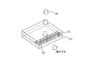
- the laser beam 124 is shaped so that the irradiation region 123 to the interface between the sapphire substrate 121 and the material layer 122 of the GaN-based compound is in a line shape, and the sapphire substrate 121 Is disclosed in which the laser beam 124 is irradiated from the back surface of the sapphire substrate 121 while moving the laser beam 124 in the direction perpendicular to the longitudinal direction of the laser beam 124.
- the time required for laser lift-off (that is, the time necessary for irradiating the entire surface of the workpiece with laser light) mainly depends on the laser light irradiation area and the workpiece conveyance speed.
- the irradiation time of the laser beam required for processing the workpiece becomes shorter if the irradiation area of the laser beam to the workpiece is large and the workpiece is conveyed at a high speed, and becomes longer if the workpiece is transferred at high speed.
- the time required for laser lift-off mainly depends on the irradiation area of the laser beam on the workpiece.
- the laser light used for laser lift-off requires irradiation energy exceeding the decomposition threshold for decomposing the material constituting the material layer, but the laser light is maintained while maintaining the irradiation energy necessary for laser lift-off. It is difficult to increase the irradiation area.
- damage such as cracks occurs in the material layer at the time of laser lift-off.
- the material layer 2 is irradiated with pulsed laser light, whereby GaN in the material layer 2 is decomposed into Ga and N 2 .
- N 2 gas is generated by the decomposition of GaN, shear stress is applied to the GaN layer, and cracks are generated at the boundary of the laser light irradiation region, thereby damaging the edge of the irradiation region. It is considered that the magnitude of damage due to this decomposition greatly depends on the irradiation area of the laser beam. That is, as the irradiation area S is larger, a larger force is applied to the edge portion of the irradiation region of the pulsed laser light, such as the generation amount of the N 2 gas is increased.
- the irradiation area of the laser beam on the workpiece in order to reduce damage to the material layer at the time of laser lift-off.
- the laser light irradiation area is reduced, there is a problem that the laser light irradiation time required for laser lift-off becomes longer.
- the irradiation time of laser light required for laser lift-off of a workpiece of ⁇ 2 inches (50.8 mm) is about 25 seconds.
- the irradiation time of the laser beam required for laser lift-off of the ⁇ 2 inch workpiece is about 625 seconds.
- FIG. 13 is a diagram illustrating an example of a light intensity distribution of laser light irradiated to irradiation regions adjacent to each other.
- the vertical axis indicates the intensity of the laser beam irradiated to each irradiation area of the workpiece, and the horizontal axis indicates the conveyance direction of the workpiece.
- L1 and L2 indicate the profiles of the laser beams irradiated to the irradiation area of the workpiece, respectively.
- the laser beams L1 and L2 need to be superimposed in an energy region exceeding the decomposition threshold VE necessary for decomposing and separating the material layer of the GaN-based compound from the sapphire substrate.
- the intensity (energy value) CE of the laser beam at the intersection position C between the laser beams L1 and L2 in the light intensity distribution of each laser beam is set to be a value exceeding the decomposition threshold value VE.
- the laser light is applied to the workpiece so that the edge portion of the adjacent irradiation region overlaps in the energy region exceeding the decomposition threshold VE. It is necessary to irradiate the entire surface, but in addition to this, it is necessary to reduce the irradiation area of the laser beam. However, when the irradiation area of the laser beam is reduced, there is a problem that the time required for the laser lift-off process increases as described above.
- the present invention solves the above-described problems, and provides a laser lift-off device capable of performing laser lift-off processing in a short time without causing a crack in a material layer formed on a substrate. For the purpose.
- a laser beam emitted from a laser source using a laser beam forming means provided with a plurality of laser beam emitting portions having a small area for dividing a laser beam such as a mask.
- a laser beam forming means provided with a plurality of laser beam emitting portions having a small area for dividing a laser beam such as a mask.
- a plurality of irradiation regions with small areas separated from each other are formed on the workpiece.
- the region irradiated with each laser beam emitted from the plurality of laser beam emitting units is referred to as an irradiation region.
- the laser beam is collectively irradiated so that the plurality of irradiation regions separated from each other are formed on the workpiece.
- the adjacent irradiation regions are spaced apart from each other so as to be arranged obliquely with respect to the movement direction of the workpiece, and the end portions extending in a direction parallel to the relative movement direction of the workpiece in the adjacent irradiation region,
- the plurality of irradiation areas are arranged so as to be sequentially overlapped as they move.
- the conveyance speed of the workpiece 3 and the irradiation interval of the pulse laser light are set so that the edge portions extending in the direction orthogonal to the workpiece conveyance direction in each irradiation region overlap each other. That is, the end portions (edge portions) of the respective irradiation regions overlap with the end portions (edge portions) of the adjacent irradiation regions.
- the irradiation area formed on the workpiece or a mask opening when a mask is used as the laser beam forming means
- the edge portion LA1 of the irradiation area LA formed by the laser light emitted from each adjacent opening provided in the mask is an irradiation area LB adjacent to the workpiece conveyance direction.
- the edge portion LB1 ′ is sequentially superimposed with a slight time interval. The same applies to LB to LJ.
- the conveyance speed of the workpiece 3 and the irradiation interval of the pulse laser beam are set so that the edge portions LA2 extending in the direction orthogonal to the conveyance direction of the workpiece in the irradiation area LA overlap each other.
- LB to LJ the same applies to LB to LJ. In this way, it is substantially the same as making the laser irradiation area on the workpiece a large area.
- the laser light (LA and LB in FIG. 5 and the like) irradiated on the workpiece in a superimposed manner is irradiated with a slight time interval since the workpiece is conveyed.
- the time until the temperature returns to room temperature after reaching the temperature at which the material layer decomposes is extremely short, approximately 100 ⁇ sec.
- the irradiation intervals of the laser beams LA and LB irradiated to the overlapping region T1 in FIG. 5 are much longer than the above 100 ⁇ sec. That is, in the laser beam superimposing region T1 shown in FIG. 5B, the laser beam LA is irradiated after the LB. However, when the laser beam LA is irradiated, the temperature of the region irradiated with the laser beam LB is already room temperature. Down to level.
- the irradiation energy of the laser beams LA and LB is not added together, so that the irradiation region of the laser beam emitted from each laser beam emitting portion becomes a substantially small area and damages the material layer. Will be reduced.
- the laser beam emitted from the laser source is divided into a plurality of laser beams by the laser beam forming means, and a plurality of irradiation regions separated from each other are formed on the workpiece by each of the divided laser beams. Since each of the irradiation areas is collectively irradiated with the laser beam, it is possible to irradiate the plurality of irradiation areas with a single laser beam irradiation.
- FIG. 1 is a diagram showing an outline of the configuration of a laser lift-off device according to an embodiment of the present invention.
- a work 3 in which a material layer 2 is formed on a substrate 1 that transmits laser light is placed on a work stage 31.
- the work stage 31 on which the work 3 is placed is placed on a transport mechanism 32 such as a conveyor, and is transported by the transport mechanism 32 at a predetermined speed.
- the workpiece 3 is irradiated with the laser beam L through the substrate 1 while being conveyed in a predetermined direction together with the workpiece stage 31.
- the workpiece 3 is formed by forming a material layer 2 of a GaN (gallium nitride) compound on the surface of a substrate 1 made of sapphire.
- the substrate 1 may be any material as long as it can form a GaN-based compound material layer satisfactorily and transmits laser light having a wavelength necessary for decomposing the GaN-based compound material layer.
- a GaN-based compound is used for the material layer 2 in order to efficiently output high-output blue light or ultraviolet light with low input energy.
- the laser beam should be appropriately selected according to the substrate 1 and the substance constituting the material layer peeled from the substrate 1.
- a KrF (krypton fluorine) excimer laser that emits a pulsed laser beam having a wavelength of 248 nm can be used.
- the light energy (5 eV) with a laser wavelength of 248 nm is between the band gap of GaN (3.4 eV) and the band gap of sapphire (9.9 eV). Therefore, a laser beam having a wavelength of 248 nm is desirable for peeling the material layer of the GaN compound from the sapphire substrate.
- a mask 44 for forming a predetermined laser beam pattern on the laser beam L emitted from the laser source is disposed above the workpiece 3. In FIG. 1, a projection lens described later is omitted.
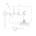
- FIG. 2 is a conceptual diagram of an optical system of the laser lift-off device according to the embodiment of the present invention.
- a laser lift-off device 100 includes a laser source 20 that generates pulsed laser light, a laser optical system 40 for shaping the laser light into a predetermined shape, a work stage 31 on which the work 3 is placed, A transport mechanism 32 that transports the work stage 31 and a controller 33 that controls the irradiation interval of the laser light generated by the laser source 20 and the operation of the transport mechanism 32 are provided.
- the laser optical system 40 includes cylindrical lenses 41 and 42, a mirror 43 that reflects the laser light in the direction of the workpiece, a mask 44 having an opening that transmits the laser light, and an image of the laser light L that has passed through the mask 44.
- the mask 44 has a plurality of openings for dividing the laser beam, divides the laser beam emitted from the laser source 2 into a plurality of laser beams, and each of the divided laser beams causes each other to be placed on the workpiece.
- a plurality of spaced irradiation regions are formed. That is, the mask 44 functions as the laser beam forming means described above, and the plurality of openings serve as laser beam emitting portions.
- the arrangement, shape, and area of the irradiation region of the pulse laser beam on the work 3 can be appropriately set by selecting the arrangement, shape, size, and the like of the opening of the mask 44 that functions as the laser beam forming unit. .
- a workpiece 3 is disposed at the tip of the laser optical system 40. The work 3 is placed on the work stage 31. The work stage 31 is placed on the transport mechanism 32 and is transported by the transport mechanism 32.
- the pulsed laser light L generated by the laser source 20 passes through the cylindrical lenses 41 and 42, the mirror 43, and the mask 44, and then is projected onto the work 3 by the projection lens 45.
- the pulse laser beam L is applied to the interface between the substrate 1 and the material layer 2 through the substrate 1.
- GaN near the interface between the material layer 2 and the substrate 1 is decomposed. In this way, the material layer 2 is peeled from the substrate 1.
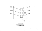
- FIG. 3 is a view showing a first embodiment of a mask provided in the laser lift-off apparatus of the present invention.
- the mask 44 of the present embodiment has a plurality of openings M1 to M5 as laser beam emitting portions spaced apart from each other in a metal plate portion, and as shown in FIG. It is drilled so as to be arranged on a straight line that is inclined with respect to the conveying direction of the workpiece 3 (arrow direction in the figure).
- the openings M1 to M5 serving as the respective laser light emitting portions emit from the adjacent laser light emitting portions (each opening of the mask) when the work 3 is conveyed in one direction.
- the irradiation areas formed by the laser light are formed apart from each other without being continuous so that the edge portions extending in the direction parallel to the conveying direction of the workpiece 3 overlap.
- the openings M1 to M5 formed in the mask 44 divide the laser beam emitted from the laser source to form a plurality of irradiation regions separated from each other.
- the area of each irradiation region is, for example, the shape of the irradiation region. When close to a square, the size is set to be 0.25 mm 2 or less.
- the irradiation area by the divided laser light is reduced as described above, damage applied to the material layer when the material layer is peeled from the substrate can be reduced. That is, as described above, when GaN is decomposed, shear stress is applied to the GaN layer, and cracks are generated at the boundary of the irradiation region of the laser light, which damages the edge of the irradiation region.
- the magnitude of the damage is considered to largely depend on the irradiation area of the laser beam.
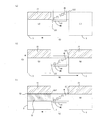
- FIG. 4A and 4B are diagrams for explaining a laser beam irradiation method according to the laser lift-off apparatus of this embodiment, where FIG. 4A shows a laser irradiation period, FIG. 4B shows a laser pause period, and FIG. 4C shows a laser irradiation period.
- the numbers in parentheses in the figure indicate the laser light irradiation procedure, and the steps (2) and (5) are executed during the laser light irradiation period (see LA and LC in FIG. 6). (3) (4) This procedure is executed during the laser light pause period (see LB in FIG. 6).
- FIG. 4A shows a laser irradiation period
- FIG. 4B shows a laser pause period
- FIG. 4C shows a laser irradiation period.
- the numbers in parentheses in the figure indicate the laser light irradiation procedure, and the steps (2) and (5) are executed during the laser light irradiation period (see LA and LC in FIG. 6).
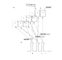
- FIG. 5 shows the scanning direction of the laser beam on the workpiece and the irradiation pattern of the laser beam on the workpiece.
- FIG. 6 shows a time chart showing the timing of laser beam irradiation and pause. (2), (3), (4), and (5) in FIG. 6 correspond to the irradiation periods (2) and (5) and the rest periods (3) and (4) in FIG. Further, FIG. 7 shows the relationship between the irradiation timing of the pulse laser beam and the irradiation area on the workpiece.
- the mask is not moved, and the pulse laser beam is irradiated while moving the workpiece, but FIG. 5 is drawn to scan the laser beam for convenience of explanation. Yes.
- the mask 44 is arranged so that the upper end of the uppermost opening M1 in the drawing is aligned with the upper end of the workpiece 3.
- the workpiece 3 is conveyed in one direction from the right to the left while irradiating the laser beam.
- the laser light passes through the mask 44 shown in FIG. 3 so that the irradiation areas LA to LE formed by the divided laser light are transformed into the work 3.
- the laser light is directed upward from the left side of the workpiece 3 to the right side of the mask 44 on the workpiece 3.
- the region S1 is irradiated from the upper end of the opening M1 located at (the imaginary line LL1 in FIG. 4) to the lower end of the opening M5 located at the lowest position of the mask 44 (the imaginary line LL2 in FIG. 4).
- the irradiation areas LA and LB, LB and LC, LC and LD, and LD and LE formed by the laser beams irradiated from the openings of the adjacent masks 44 are respectively workpieces.
- edge portions LA1 and LB1 ′ extending in a direction parallel to the moving direction of the workpiece 3 are superimposed on each other (the same applies to LB, LC, LD,...), And an overlapping region T1 is formed. Irradiated as follows.
- the transport speed of the work 3 and the pulse laser beam are superposed so that the edge portions LA2, LB2,...
- the irradiation interval is set.
- the pulse interval of the laser beam is set to be shorter than the time required for the work to move a distance corresponding to the irradiation region for one shot of the laser beam. For example, when the conveying speed of the workpiece 3 is 100 mm / second and the width of the laser light overlapping region ST is 0.1 mm, the pulse interval of the laser light is 0.004 seconds (250 Hz).
- FIG. 7 is a diagram showing the relationship between the irradiation timing of the pulse laser beam and the irradiation area on the workpiece, (A) shows an irradiation area on the workpiece, (b) shows each pulse laser beam, and in the drawing, the laser beam is irradiated in the order of irradiation areas A ⁇ B ⁇ C on the workpiece.
- the region A is irradiated with the laser beam a
- the irradiation region B is irradiated with the laser beam b
- the irradiation region C is irradiated with the laser beam c.
- the work laser 3 passes through the opening of the mask 44 and is irradiated onto the irradiation area A on the work 3 until the next pulse laser light b is irradiated. It moves to the position where the laser beam is irradiated to the irradiation region. Then, the next pulse laser beam b is applied at a timing such that an edge portion (a hatched portion in the figure) T3 extending in a direction orthogonal to the conveyance direction of the workpiece 3 in the irradiation region A and the irradiation region B overlaps. 3 is irradiated to the irradiation region B on the upper side.
- the workpiece 3 moves to a position where the irradiation region C in the figure is irradiated with the laser beam, and the next pulse laser beam c is applied to the irradiation region B. Irradiation is performed at such a timing that the edge portions of the irradiation region C (hatched portions in the figure) overlap each other.
- the procedures (3) and (4) shown in FIG. 4 are executed during a pause period of the pulse laser beam (see FIG. 6), and preparation for irradiating the next region of the workpiece 3 with the laser beam is performed.
- the procedure of (3) in order to irradiate the next region of the workpiece with the laser beam, the workpiece 3 is moved to a distance slightly shorter than the laser-irradiated region S1 of FIG. Is conveyed in the direction of the arrow (3).
- the reason why the transport distance of the workpiece 3 is slightly shorter than the region S1 irradiated with the laser is to superimpose the regions S1 and S2 irradiated with the laser beam shown in FIG. 4C in the procedure (5) described later.
- the procedure (4) in order to make the moving direction of the work 3 relative to the mask 44 the same as the moving direction (2) during the pause period of the pulse laser beam, the work is moved from the left according to the arrow (4) in FIG. Carry to the right.
- the workpiece 3 is conveyed in one direction from the right to the left according to the arrow (5) in FIG.
- the irradiation areas LF to LJ formed by the laser beam are arranged on a straight line inclined with respect to the workpiece conveyance direction, and the laser beam is placed on the left side of the workpiece 3.
- the laser beam is placed on the left side of the workpiece 3.
- the irradiation areas LF and LG, LG and LH, LH and LI, and LI and LJ formed by the laser beams irradiated from the adjacent laser beam emitting portions are the movement directions of the workpiece. Irradiation is performed so that the edge portions extending in the direction parallel to and overlap. Further, in the procedure of (3), by adjusting the transport distance of the workpiece 3 as described above, the regions S1 and S2 to be irradiated with laser light are superimposed (superimposed region T2). Further, as described with reference to FIG.
- the laser beams LF to LJ are irradiated so that the edge portions of the respective irradiation regions extending in the direction orthogonal to the conveyance direction of the workpiece 3 are overlapped.
- the entire surface of the workpiece 3 is irradiated with laser light.
- the mask 44 having a plurality of openings M1-M5 (corresponding to the laser beam emitting portions) arranged apart from each other is provided as the laser beam forming means, and the openings M1-M5 of the mask 44 are provided.
- the laser beam LA-LE divided by the laser beam LA-LE forms irradiation regions spaced from each other on the workpiece, and the irradiation region of the workpiece formed by the laser beams LA-LE emitted from the adjacent openings M1-M5.
- Edge portions extending in a direction parallel to the moving direction are configured to be collectively irradiated onto the workpiece while being sequentially superimposed as the workpiece is moved in one direction.
- the laser beams LA to LE emitted from the laser beam emitting units arranged apart from each other are sequentially superimposed at intervals as described above. For this reason, the irradiation energy of each divided
- the laser beam LA is irradiated after LB, but since the time until the material layer returns from the decomposition temperature to room temperature is extremely short, when LA is irradiated, the region already irradiated by LB is already at room temperature. Therefore, the irradiation energy of the laser beams LA and LB is not summed.
- each laser beam divided by the mask 44 is the same as being individually irradiated onto the workpiece, and each laser irradiation region has a small area. For this reason, damage to the material layer when the material layer is peeled from the substrate can be reduced.
- the scanning direction of the laser beam with respect to the workpiece is always the same, but the scanning direction is always the same. There is no need.
- FIG. 8 is a view showing a second embodiment of the mask used in the laser lift-off apparatus of the present invention.
- the openings M1 to M6 serving as laser beam emitting portions are formed so as not to be continuous with each other and are arranged in a staggered manner. That is, at least two rows of one or more openings are arranged linearly in a direction orthogonal to the movement direction of the workpiece, and the openings in one row and the openings in the other row are in relation to the movement direction of the workpiece. Arranged in an oblique direction.
- each of the openings M1 to M6 is provided in the irradiation region formed by the laser beam emitted from the openings (for example, the openings M1 and M2) adjacent to the direction orthogonal to the workpiece conveyance direction when the workpiece 3 is conveyed.
- the edge portions extending in the direction parallel to the transport direction 3 are arranged so as to overlap. Even when the shape of the mask 44 is as described above, the end portions (edge portions) of the respective irradiation regions are mutually connected to the end portions (edge portions) of the adjacent irradiation regions in the same manner as described in the mask of the first embodiment. Similar to the first embodiment, the laser lift-off process can be performed in a short time, and the throughput can be improved.
- FIG. 9 is a conceptual diagram of an optical system of a laser lift-off device when other laser light forming means is used
- FIG. 10 is an enlarged view of the laser light forming means shown in FIG. a) is an enlarged view of the vicinity of the workpiece
- FIG. 5 (b) is a view showing the arrangement of the light emitting elements.
- the laser beam forming means is composed of light guides 61a to 61e, light emitting elements 62a to 62e, and optical fibers 60a to 60e
- the laser beam emitting part corresponding to the opening of the mask is the light emitting elements 62a to 62e.
- the plurality of light emitting elements 62a to 62e are straightly inclined with respect to the conveying direction of the workpiece 3, like the mask openings M1 to M5 shown in FIG.
- Each of the light emitting elements 62a to 62e is arranged on a line, and for example, as shown in FIG. 5, the laser light emitted from each adjacent laser light emitting portion when the work 3 is conveyed in one direction, as shown in FIG. Are arranged so as to be separated from each other so that the edge portions extending in the direction parallel to the conveyance direction of the workpiece 3 overlap in the irradiation region formed by the above.
- the light emitting elements 62a to 62e are arranged in a straight line like the openings M1 to M5 of the mask shown in FIG. 3, but they may be arranged in a staggered manner as shown in FIG.
- a method for manufacturing a semiconductor light-emitting element that can use the above-described laser lift-off device will be described.
- the manufacturing method of the semiconductor light-emitting device formed of a GaN-based compound material layer will be described with reference to FIG.
- a sapphire substrate capable of crystal growth of a gallium nitride (GaN) compound semiconductor that transmits laser light and forms a material layer is used.
- GaN gallium nitride
- FIG. 11A a GaN layer 102 made of a GaN-based compound semiconductor is rapidly formed on a sapphire substrate 101 by using, for example, a metal organic chemical vapor deposition method (MOCVD method). Subsequently, as illustrated in FIG.
- MOCVD method metal organic chemical vapor deposition method
- an n-type semiconductor layer 103 and a p-type semiconductor layer 104 that are light emitting layers are stacked on the surface of the GaN layer 102.
- GaN doped with silicon is used as the n-type semiconductor
- GaN doped with magnesium is used as the p-type semiconductor.
- solder 105 is applied on the p-type semiconductor layer 104.
- the support substrate 106 is attached on the solder 105.
- the support substrate 106 is made of, for example, an alloy of copper and tungsten. Then, as shown in FIG.
- the laser beam 107 is irradiated from the back surface side of the sapphire substrate 101 toward the interface between the sapphire substrate 101 and the GaN layer 102.
- the GaN layer 102 is peeled from the sapphire substrate 101.
- ITO 108 which is a transparent electrode is formed on the surface of the GaN layer 102 after peeling by vapor deposition, and the electrode 109 is attached to the surface of the ITO 108.
Landscapes
- Physics & Mathematics (AREA)
- Optics & Photonics (AREA)
- Engineering & Computer Science (AREA)
- Plasma & Fusion (AREA)
- Mechanical Engineering (AREA)
- Chemical & Material Sciences (AREA)
- Chemical Kinetics & Catalysis (AREA)
- General Chemical & Material Sciences (AREA)
- Oil, Petroleum & Natural Gas (AREA)
- Laser Beam Processing (AREA)
- Recrystallisation Techniques (AREA)
Abstract
Description
例えば、特許文献1においては、サファイア基板の上にGaN層を形成し、当該サファイア基板の裏面からレーザ光を照射することにより、GaN層を形成するGaNが分解され、当該GaN層をサファイア基板から剥離する技術について記載されている。以下では基板上に材料層が形成されたものをワークと呼ぶ。
GaN系化合物材料層を基板からレーザリフトオフするためには、GaN系化合物をGaとN2とに分解するために必要な照射エネルギーを有するレーザ光をワークの全面に亘り照射することが重要になる。
しかしながら、ワークの搬送速度には自ずと限界がある。よって、レーザリフトオフに要する時間は、主としてワークへのレーザ光の照射面積に依存する。ところが、ワークへのレーザ光の照射面積を大きくすることは、次に説明するように様々な困難が伴う。
即ち、レーザリフトオフに使用されるレーザ光には、材料層を構成する物質を分解するための分解閾値を超える照射エネルギーが必要とされるが、レーザリフトオフに必要な照射エネルギーを維持しつつレーザ光の照射面積を大きくすることは困難である。
本発明者らが鋭意検討したところ、ワークへのレーザ光の照射面積を大きくした場合は、レーザリフトオフ時に材料層に例えばクラック(割れ)などのダメージが発生することが判明した。
前述したように、材料層2はパルスレーザ光が照射されることにより、材料層2のGaNがGaとN2とに分解する。GaNが分解することによりN2ガスが発生することから、当該GaN層にせん断応力が加わり、当該レーザ光の照射領域の境界部においてクラックが生じるなど、照射領域のエッジ部にダメージを与える。
この分解によるダメージの大きさは、レーザ光の照射面積に大きく依存しているものと考えられる。すなわち、照射面積Sが大きいほど、上記N2ガスの発生量が多くなる等、パルスレーザ光の照射領域のエッジ部へ大きな力が加わる。
しかしながら、レーザ光照射面積を小さくすると、レーザリフトオフに要するレーザ光の照射時間が長くなるという問題がある。例えば、以下の条件1では、φ2インチ(50.8mm)のワークをレーザリフトオフするために要するレーザ光の照射時間は約25秒である。一方、以下の条件2では、φ2インチのワークをレーザリフトオフするために要するレーザ光の照射時間は約625秒となる。
(条件1)
・ワークの直径:φ2インチ
・ワークへのレーザ光の照射領域:1mm角の正方形
・パルスレーザ光の周波数:100Hz
(条件2)
・ワークの直径:φ2インチ
・ワークへのレーザ光の照射領域:0.2mm角の正方形
・パルスレーザ光の周波数:100Hz
以上のように、レーザ光の照射面積を大きくすると、レーザリフトオフ処理に要する時間が小さくなるものの材料層へのダメージが大きくなり、また、照射面積を小さくすると、材料層へのダメージは小さくなるもののレーザリフトオフ処理に要する時間が増加するといった、相反する問題が生ずる。
分解閾値以上の照射エネルギーを有するレーザ光が照射されない領域が存在すると、材料層を構成するGaNの未分解領域が形成され、材料層を基板から十分に剥離させることができない。このため、隣り合う照射領域のエッジ部が、分解閾値VEを超えるエネルギー領域において重畳する必要がある。
図13は、互いに隣接する照射領域に照射されるレーザ光の光強度分布の一例を示す図である。同図において縦軸はワークの各照射領域に照射されるレーザ光の強度を、横軸はワークの搬送方向を示す。また、L1、L2は、それぞれワークの照射領域に照射されるレーザ光のプロファイルを示す。
図13に示すように、レーザ光L1、L2は、GaN系化合物の材料層を分解してサファイアの基板から剥離させるために必要な分解閾値VEを超えるエネルギー領域において重畳させる必要がある。
しかし、レーザ光の照射面積を小さくすると、前述したように、レーザリフトオフ処理に要する時間が増加するといった問題が生ずる。
本発明は上記問題点を解決するものであって、基板上に形成された材料層に割れを生じさせることなく、しかも、レーザリフトオフ処理を短時間に行うことが可能なレーザリフトオフ装置を提供することを目的とする。
そして、ワークあるいはレーザ源(照射領域)を相対的に移動させながら、ワーク上に、上記互いに離間した複数の照射領域が形成されるように、レーザ光を一括照射する。
その際、隣り合う照射領域が、上記ワークの移動方向に対して斜めに配置されるように互いに離間させ、隣接する照射領域のワークの相対的移動方向に対して平行方向に伸びる端部が、移動するに従って順次に重畳するように上記複数の照射領域を配列する。さらに、各照射領域におけるワークの搬送方向と直交方向に伸びるエッジ部が互いに重畳するように、ワーク3の搬送速度とパルスレーザ光の照射間隔を設定する。
すなわち、上記各照射領域の端部(エッジ部)は隣接する照射領域の端部(エッジ部)と互いに重畳する。
上記ワーク上に形成される照射領域(レーザ光形成手段としてマスクを用いた場合はマスクの開口)は、具体的には、ワークの移動方向に対して傾斜した一直線上になるように配列したり、あるいは、千鳥状に配列される。
マスクに設けられた隣接する各開口から出射するレーザ光により形成される照射領域LAのエッジ部LA1は、後述する図5に示すように、ワークの搬送方向と直交方向に隣接する照射領域LBのエッジ部LB1´と、ワークを搬送するに従って、わずかな時間を隔てて順次に重畳する。LB~LJについても同様である。
また、ワーク3の搬送速度とパルスレーザ光の照射間隔は、照射領域LAにおけるワークの搬送方向と直交方向に伸びるエッジ部LA2が互いに重畳するように設定される。LB~LJについても同様である。このようにすれば、実質的にワークへのレーザ照射領域を大面積にしたことと同じになる。
なお、ワーク上で重畳して照射されるレーザ光(図5のLAとLBなど)は、ワークを搬送していることから、わずかながらも時間を隔てて照射される。材料層がGaN(ガリウムナイトライド)系化合物である場合は、材料層が分解する温度に達した後に室温に戻るまでの時間は極めて短く、概ね100μ秒程度である。これに対し、図5の重畳領域T1に照射されるレーザ光LA、LBの各々の照射間隔は上記の100μ秒よりもはるかに長い。つまり、図5(b)に示すレーザ光重畳領域T1では、レーザ光LAがLBよりも後に照射されるが、レーザ光LAの照射時において、レーザ光LBが照射された領域の温度が既に室温レベルに下がっている。したがって、重畳領域T1では、レーザ光LAとLBのそれぞれの照射エネルギーが合算されないので、各々のレーザ光出射部から出射したレーザ光の照射領域が実質的に小面積になり、材料層へのダメージは低減されることになる。
(1)レーザ光形成手段により、レーザ源から出射するレーザ光を、複数のレーザ光に分割し、分割された各レーザ光により前記ワーク上に互いに離間した複数の照射領域を形成し、ワーク上の各照射領域にレーザ光を一括照射するようにしたので、一度のレーザ光の照射で複数の照射領域にレーザ光を照射することができる。すなわち、複数の照射領域に一括してレーザ光を照射することができるので、各照射領域を小面積にしても、レーザリフトオフ処理を短時間に行うことができ、スループットの向上を図ることができる。
(2)隣接する各レーザ光出射部から出射したレーザ光の、ワークの移動方向と平行方向に伸びるエッジ部がワークの移動に従って順次に重畳されるようにするとともに、各照射領域におけるワークの搬送方向と直交方向に伸びるエッジ部が互いに重畳するようにしたので、GaN系化合物をGaとN2とに分解するために必要な分解閾値以上の照射エネルギーを有するレーザ光を、各照射面積を小さくしながら、ワークの全面に亘り照射することができる。
また、前述したように重畳領域に照射されるレーザ光は、照射された領域の温度が低下するに充分な時間間隔をおいて照射されるので、重畳領域に照射されるレーザ光のそれぞれの照射エネルギーが合算されることはない。したがって、各照射領域が重畳していても、実質的に各照射領域毎にレーザ光を照射したのと同等の効果を得ることができる。このため、材料層を基板から剥離するときの材料層へのダメージを低減化することができる。
同図に示すレーザリフトオフ装置は、レーザ光を透過する基板1上に材料層2が形成されたワーク3が、ワークステージ31上に載置されている。ワーク3を載せたワークステージ31は、コンベヤのような搬送機構32に載置され、搬送機構32によって所定の速度で搬送される。ワーク3は、ワークステージ31と共に所定方向に搬送されながら、基板1を通じてレーザ光Lが照射される。
ワーク3は、サファイアからなる基板1の表面に、GaN(窒化ガリウム)系化合物の材料層2が形成されてなるものである。基板1は、GaN系化合物の材料層を良好に形成することができ、尚且つ、GaN系化合物材料層を分解するために必要な波長のレーザ光を透過するものであれば良い。材料層2には、低い入力エネルギーによって高出力の青色光あるいは紫外光を効率良く出力するためにGaN系化合物が用いられる。
同図において、レーザリフトオフ装置100は、パルスレーザ光を発生するレーザ源20と、レーザ光を所定の形状に成形するためのレーザ光学系40と、ワーク3が載置されるワークステージ31と、ワークステージ31を搬送する搬送機構32と、レーザ源20で発生するレーザ光の照射間隔および搬送機構32の動作を制御する制御部33とを備えている。
レーザ光学系40は、シリンドリカルレンズ41、42と、レーザ光をワークの方向へ反射するミラー43と、レーザ光を透過させる開口を有するマスク44と、マスク44を通過したレーザ光Lの像をワーク3上に投影する投影レンズ45とを備えている。上記マスク44は、レーザ光を分割するための複数の開口を有し、上記レーザ源2から出射するレーザ光を、複数のレーザ光に分割し、分割された各レーザ光により前記ワーク上に互いに離間した複数の照射領域を形成する。すなわち、マスク44は前記したレーザ光形成手段として機能し、上記複数の開口はレーザ光出射部となる。
ワーク3へのパルスレーザ光の照射領域の配置、形状、面積は、上記レーザ光形成手段として機能するマスク44の開口の配置、形状、大きさ等を選定することにより、適宜設定することができる。レーザ光学系40の先にはワーク3が配置されている。ワーク3はワークステージ31上に載置されている。ワークステージ31は搬送機構32に載置されており、搬送機構32によって搬送される。
マスク44に形成された開口M1~M5は、レーザ源から発したレーザ光を分割し互いに離間した複数の照射領域を形成するものであり、各々の照射領域の面積は、例えば照射領域の形状が正方形に近い場合には、0.25mm2以下になるような大きさに設定されている。
すなわち、前述したように、GaNが分解する際、GaN層にせん断応力が加わり、当該レーザ光の照射領域の境界部においてクラックが生じるなど、照射領域のエッジ部にダメージを与えるが、この分解によるダメージの大きさは、レーザ光の照射面積に大きく依存しているものと考えられる。
実験等を行って検証した結果、上記のように照射領域の形状が正方形に近い場合には、ワークへのレーザ光の照射面積を0.25mm2以下とすれば、ワークの材料層へのクラックの発生を防止することができることが確認された。
図4は、本実施例のレーザリフトオフ装置に係るレーザ光照射方法を説明する図であり、(a)はレーザ照射期間、(b)はレーザ休止期間、(c)はレーザ照射期間を示す。また、同図中の括弧数字はレーザ光照射の手順を示し、(2)(5)の手順をレーザ光の照射期間(図6のLA,LC参照)に実行し、(3)(4)の手順をレーザ光の休止期間(図6のLB参照)に実行する。
また、図5は、ワーク上でのレーザ光のスキャン方向とワークへのレーザ光の照射パターンを示し、図6はレーザ光の照射及び休止のタイミングを示すタイムチャートを示す。図6の(2)(3)(4)(5)は、図4の照射期間(2)(5)と休止期間(3)(4)に対応している。さらに、図7はパルスレーザ光の照射タイミングとワーク上の照射領域の関係を示す。
なお、本実施例のレーザリフトオフ装置においては、マスクは移動せず、ワークを移動させながらパルスレーザ光を照射するが、図5は、説明の都合上、レーザ光をスキャンするように描かれている。
ここで、レーザ光は、前記図3に示したマスク44を介することによって、図5(a)(b)に示すように、分割されたレーザ光により形成される照射領域LA~LEがワーク3の搬送方向に対して傾斜した一直線上に配列され、図4(a)に示すように、ワーク3の左方から右方に向けて当該レーザ光が、ワーク3上において、マスク44の最も上方に位置する開口M1の上端(図4の仮想線LL1)から、マスク44の最も下方に位置する開口M5の下端(図4の仮想線LL2)に亘る領域S1に照射される。
また、ワーク3を一方向に搬送したときに、各照射領域におけるワーク3の搬送方向と直交方向に伸びるエッジ部LA2,LB2,…が互いに重畳するように、ワーク3の搬送速度とパルスレーザ光の照射間隔が設定されている。
レーザ光のパルス間隔は、ワークがレーザ光の1ショット分の照射領域に相当する距離を移動するために要する時間よりも短く設定される。例えば、ワーク3の搬送速度が100mm/秒、レーザ光の重畳領域STの幅が0.1mmである場合、レーザ光のパルス間隔は0.004秒(250Hz)である。
同図(a)はワーク上の照射領域を示し、(b)は各パルスレーザ光を示しており、同図は、ワーク上の照射領域A→B→Cの順にレーザ光が照射され、照射領域Aにはレーザ光aが照射され、照射領域Bにはレーザ光bが照射され、照射領域Cにはレーザ光cが照射される場合を示している。
図7において、パルスレーザ光aがマスク44の開口を通過してワーク3上の照射領域Aに照射され、次のパルスレーザ光bが照射されるまでの間に、ワーク3は同図のBの照射領域にレーザ光が照射される位置まで移動する。
そして、次のパルスレーザ光bは、上記照射領域Aと照射領域Bのワーク3の搬送方向と直交方向に伸びるエッジ部(同図のハッチングを付した部分)T3が重畳するようなタイミングでワーク3上の照射領域Bに照射される。
同様に、次のパルスレーザ光cが照射されるまでの間に、ワーク3は同図の照射領域Cにレーザ光が照射される位置まで移動し、次のパルスレーザ光cは、照射領域Bと照射領域Cのエッジ部(同図のハッチングを付した部分)が互いに重畳するようなタイミングで照射される。
(3)の手順では、ワークの次なる領域にレーザ光を照射するために、レーザ光の休止期間において、図4(a)のレーザ照射した領域S1よりもやや短い距離だけワーク3を図4に示す矢印(3)の方向に搬送する。ワーク3の搬送距離をレーザ照射した領域S1よりやや短くするのは、後述の(5)の手順において、図4(c)に示すレーザ光を照射する領域S1とS2とを重畳させるためである。(4)の手順では、パルスレーザ光の休止期間中に、マスク44に対するワーク3の移動方向を(2)の移動方向と同じにするため、図4の矢印(4)に従ってワークを左方から右方に搬送する。
図5(b)に示すように、それぞれ隣接するレーザ光出射部から照射されるレーザ光により形成される照射領域LFとLG、LGとLH、LHとLI、LIとLJは、ワークの移動方向と平行方向に伸びるエッジ部が重畳するように照射される。
また、(3)の手順において、前記のようにワーク3の搬送距離を調整することにより、レーザ光照射する領域S1とS2とを重畳させる(重畳領域T2)。
さらに、レーザ光LF~LJは、前記図7で説明したように、ワーク3の搬送方向と直交方向に伸びる各照射領域のエッジ部が重畳するように照射される。
このような手順(1)~(5)を繰返し実行することにより、ワーク3の全面に亘りレーザ光が照射される。
しかも、上記実施例は、互いに離間して配置されるレーザ光出射部から出射した各レーザ光LA~LEが、前記したように時間を隔てて順次に重畳される。
このため、分割された各レーザ光の照射エネルギーが合算されることがない。例えば、レーザ光LAはLBよりも後に照射されるが、材料層が分解温度から室温に戻るまでの時間が極めて短いことから、LAが照射される時にはLBによって既に照射された領域は既に室温状態になっているため、レーザ光LAとLBの照射エネルギーは合算されない。つまり、マスク44によって分割された各レーザ光は、個別にワークに照射されるのと同然であり、各々のレーザ照射領域が小面積となる。このため、基板から材料層を剥離する際の材料層へのダメージを軽減することができる。
なお、図4に示した手順においては、図5(a)に示すように、ワークに対するレーザ光のスキャン方向が常に同じになるようにしているが、必ずしもスキャン方向を常に同じになるようにする必要はない。
図8に示すマスク44は、レーザ光出射部となる各々の開口M1-M6が、互いに連続することなく離間して形成され、千鳥状に配列されている。
すなわち、少なくとも2列の一乃至複数の開口が、前記ワークの移動方向と直交方向に直線状に配列され、一方の列の開口と、他方の列の開口は、前記ワークの移動方向に対して斜め方向に配列される。
さらに、各々の開口M1-M6は、ワーク3を搬送したときに、ワーク搬送方向に直交する方向に隣接する開口(例えば開口M1とM2)から出射するレーザ光により形成される照射領域の、ワーク3の搬送方向に平行方向に伸びるエッジ部が重畳するように配列されている。
マスク44の形状を上記のようにしても、前記第1の実施例のマスクで説明したのと同様各照射領域の端部(エッジ部)を隣接する照射領域の端部(エッジ部)と互いに重畳させることができ、第1の実施例と同様、レーザリフトオフ処理を短時間に行うことができ、スループットの向上を図ることができる。
本実施例においては、レーザ光形成手段が導光部61a~61eと光出射素子62a~62eと光ファイバ60a~60eから構成され、マスクの開口に相当するレーザ光出射部は光出射素子62a~62eに対応する。
すなわち、図10(a)(b)に示すように、複数の光出射素子62a-62eが、図3に示したマスクの開口M1~M5と同様、ワーク3の搬送方向に対して傾斜する一直線上に配列されており、各々の光出射素子62a-62eは、例えば前記図5に示したように、ワーク3を一方向に搬送したときに、隣接する各レーザ光出射部から出射するレーザ光により形成される照射領域の、ワーク3の搬送方向と平行方向に伸びるエッジ部が重畳するように、互いに離間して配置されている。
なお、図10では、光出射素子62a~62eを図3に示したマスクの開口M1~M5と同様、直線状に配列したが、図8に示したように千鳥状に配列してもよい。
結晶成長用の基板には、レーザ光を透過し材料層を構成する窒化ガリウム(GaN)系化合物半導体を結晶成長させることができるサファイア基板を使用する。図11(a)に示すように、サファイア基板101上には、例えば有機金属気相成長法(MOCVD法)を用いて迅速にGaN系化合物半導体よりなるGaN層102が形成される。
続いて、図11(b)に示すように、GaN層102の表面には、発光層であるn型半導体層103とp型半導体層104とを積層させる。例えば、n型半導体としてはシリコンがドープされたGaNが用いられ、p型半導体としてはマグネシウムがドープされたGaNが用いられる。
続いて、図11(c)に示すように、p型半導体層104上には、半田105が塗布される。続いて、図11(d)に示すように、半田105上にサポート基板106が取付けられる。サポート基板106は例えば銅とタングステンの合金からなる。
そして、図11(e)に示すように、サファイア基板101の裏面側からサファイア基板101とGaN層102との界面に向けてレーザ光107を照射する。
レーザ光107をサファイア基板101とGaN層102の界面に照射して、GaN層102を分解することにより、サファイア基板101からGaN層102を剥離する。剥離後のGaN層102の表面に透明電極であるITO108を蒸着により形成し、ITO108の表面に電極109を取付ける。
2 材料層
3 ワーク
10 レーザリフトオフ装置
20 レーザ源
31 ワークステージ
32 搬送機構
33 制御部
40 レーザ光学系
41、42 シリンドリカルレンズ
43 ミラー
44 マスク
45 投影レンズ
60a~60e ファイバ
61a~61e 導光部
62a~62e 光出射素子
101 サファイア基板
102 GaN層
103 n型半導体層
104 p型半導体層
105 半田
106 サポート基板
107 レーザ光
108 透明電極(ITO)
109 電極
L,L1,L2 レーザ光
M1~M5 マスクの開口
LE エッジ部
VE 分解閾値
Claims (4)
- 基板上に材料層が形成されてなるワークに対し、前記基板を通してレーザ光を照射するレーザ源と、前記ワークと前記レーザ源とを相対的に移動させる搬送機構とを備えるレーザリフトオフ装置であって、
前記レーザ源から出射するレーザ光を、複数のレーザ光に分割し、分割された各レーザ光により前記ワーク上に互いに離間した複数の照射領域を形成するレーザ光形成手段を有し、
前記レーザ光形成手段により形成される複数の照射領域は、隣接する照射領域の前記ワークの移動方向と平行方向に伸びる端部が、前記ワークが前記レーザ源に対して相対的に一方向に移動するに従って、順次に重畳するように配列される
ことを特徴とするレーザリフトオフ装置。 - 前記レーザ光形成手段は、複数の方形状の開口を有するマスクである
ことを特徴とする請求項1記載のレーザリフトオフ装置。 - 前記ワーク上に形成される照射領域は、前記ワークの移動方向に対して傾斜した一直線上に配列されることを特徴とする請求項1または請求項2記載のレーザリフトオフ装置。
- 前記ワーク上に形成される照射領域は、千鳥状に配列されることを特徴とする請求項1または請求項2記載のレーザリフトオフ装置。
Priority Applications (3)
| Application Number | Priority Date | Filing Date | Title |
|---|---|---|---|
| KR1020117007136A KR101103211B1 (ko) | 2010-08-04 | 2010-09-28 | 레이저 리프트 오프 장치 |
| US13/813,645 US8742289B2 (en) | 2010-08-04 | 2010-09-28 | Laser lift-off apparatus |
| CN201080068001.XA CN102986005B (zh) | 2010-08-04 | 2010-09-28 | 激光剥离装置 |
Applications Claiming Priority (2)
| Application Number | Priority Date | Filing Date | Title |
|---|---|---|---|
| JP2010-175245 | 2010-08-04 | ||
| JP2010175245A JP4661989B1 (ja) | 2010-08-04 | 2010-08-04 | レーザリフトオフ装置 |
Publications (1)
| Publication Number | Publication Date |
|---|---|
| WO2012017565A1 true WO2012017565A1 (ja) | 2012-02-09 |
Family
ID=43952818
Family Applications (1)
| Application Number | Title | Priority Date | Filing Date |
|---|---|---|---|
| PCT/JP2010/066793 Ceased WO2012017565A1 (ja) | 2010-08-04 | 2010-09-28 | レーザリフトオフ装置 |
Country Status (6)
| Country | Link |
|---|---|
| US (1) | US8742289B2 (ja) |
| JP (1) | JP4661989B1 (ja) |
| KR (1) | KR101103211B1 (ja) |
| CN (1) | CN102986005B (ja) |
| TW (1) | TW201208106A (ja) |
| WO (1) | WO2012017565A1 (ja) |
Families Citing this family (14)
| Publication number | Priority date | Publication date | Assignee | Title |
|---|---|---|---|---|
| JP4948629B2 (ja) * | 2010-07-20 | 2012-06-06 | ウシオ電機株式会社 | レーザリフトオフ方法 |
| JP5712700B2 (ja) * | 2011-03-14 | 2015-05-07 | ウシオ電機株式会社 | レーザリフトオフ装置 |
| KR101831735B1 (ko) | 2012-10-18 | 2018-02-23 | 디앤에이 주식회사 | 레이저 리프트 오프용 기판 정렬 장치 |
| KR101373421B1 (ko) * | 2012-10-18 | 2014-03-13 | 한양대학교 산학협력단 | 웨이퍼 절단 장치 |
| EP2912685B1 (en) * | 2012-10-26 | 2020-04-08 | RFHIC Corporation | Semiconductor devices with improved reliability and operating life and methods of manufacturing the same |
| KR20160049382A (ko) | 2014-10-27 | 2016-05-09 | 삼성디스플레이 주식회사 | 레이저 박리 장치 및 표시 장치의 제조 방법 |
| KR102354971B1 (ko) | 2015-03-20 | 2022-01-25 | 삼성디스플레이 주식회사 | 디스플레이 제조방법 및 이에 사용될 수 있는 디스플레이 제조장치 |
| JP2018523291A (ja) * | 2015-06-01 | 2018-08-16 | エバナ テクノロジーズ ユーエービー | 半導体加工対象物のスクライブ方法 |
| JP6564301B2 (ja) * | 2015-10-26 | 2019-08-21 | 東京応化工業株式会社 | 支持体分離方法 |
| KR101600913B1 (ko) | 2016-01-22 | 2016-03-08 | 주식회사 덕인 | 레이저 리프트 오프 장치 및 그를 이용한 레이저 리프트 오프 방법 |
| KR101918538B1 (ko) * | 2016-03-03 | 2018-11-15 | 에이피시스템 주식회사 | 레이저 리프트 오프 공정 간 대상물 반전 검출 방법 |
| KR102297791B1 (ko) * | 2019-11-13 | 2021-09-03 | 한국광기술원 | 레이저를 이용하여 전사 대상물을 분리하고 전사하는 장치 및 방법 |
| DE102022114637A1 (de) | 2022-06-10 | 2023-12-21 | Trumpf Laser Gmbh | Verfahren und Vorrichtung zum Verarbeiten mindestens eines Teilbereichs eines Schichtsystems |
| JP2024042807A (ja) * | 2022-09-16 | 2024-03-29 | キオクシア株式会社 | レーザー加工装置、レーザー剥離方法および半導体装置の製造方法 |
Citations (5)
| Publication number | Priority date | Publication date | Assignee | Title |
|---|---|---|---|---|
| JP2001501778A (ja) * | 1996-10-01 | 2001-02-06 | シーメンス アクチエンゲゼルシヤフト | 2つの材料層を相互に分離する方法及びこの方法により製造された電子部品 |
| JP2003168820A (ja) * | 2001-12-03 | 2003-06-13 | Sony Corp | 剥離方法、レーザー光の照射方法及びこれらを用いた素子の製造方法 |
| JP2003282441A (ja) * | 2002-03-11 | 2003-10-03 | Sharp Corp | 半導体結晶層の製造方法および半導体基板、液晶ディスプレイパネル |
| JP2007149988A (ja) * | 2005-11-28 | 2007-06-14 | Tokyo Institute Of Technology | レーザーリフトオフ法およびレーザーリフトオフ装置 |
| JP2007534164A (ja) * | 2004-03-29 | 2007-11-22 | ジェイピー・サーセル・アソシエイツ・インコーポレーテッド | 材料層の分離方法 |
Family Cites Families (5)
| Publication number | Priority date | Publication date | Assignee | Title |
|---|---|---|---|---|
| JP3374413B2 (ja) * | 1992-07-20 | 2003-02-04 | 株式会社ニコン | 投影露光装置、投影露光方法、並びに集積回路製造方法 |
| JP4408361B2 (ja) * | 2003-09-26 | 2010-02-03 | 株式会社ディスコ | ウエーハの分割方法 |
| JP4941172B2 (ja) | 2007-08-22 | 2012-05-30 | 日立電線株式会社 | Iii−v族窒化物半導体自立基板及びiii−v族窒化物半導体自立基板の製造方法 |
| CN101221902B (zh) * | 2008-02-03 | 2010-11-24 | 友达光电股份有限公司 | 应用于连续性侧向长晶技术的掩膜以及激光结晶方法 |
| JP5379384B2 (ja) * | 2008-02-15 | 2013-12-25 | サイバーレーザー株式会社 | レーザによる透明基板の加工方法および装置 |
-
2010
- 2010-08-04 JP JP2010175245A patent/JP4661989B1/ja not_active Expired - Fee Related
- 2010-09-28 CN CN201080068001.XA patent/CN102986005B/zh not_active Expired - Fee Related
- 2010-09-28 KR KR1020117007136A patent/KR101103211B1/ko not_active Expired - Fee Related
- 2010-09-28 US US13/813,645 patent/US8742289B2/en not_active Expired - Fee Related
- 2010-09-28 WO PCT/JP2010/066793 patent/WO2012017565A1/ja not_active Ceased
- 2010-10-27 TW TW099136705A patent/TW201208106A/zh not_active IP Right Cessation
Patent Citations (5)
| Publication number | Priority date | Publication date | Assignee | Title |
|---|---|---|---|---|
| JP2001501778A (ja) * | 1996-10-01 | 2001-02-06 | シーメンス アクチエンゲゼルシヤフト | 2つの材料層を相互に分離する方法及びこの方法により製造された電子部品 |
| JP2003168820A (ja) * | 2001-12-03 | 2003-06-13 | Sony Corp | 剥離方法、レーザー光の照射方法及びこれらを用いた素子の製造方法 |
| JP2003282441A (ja) * | 2002-03-11 | 2003-10-03 | Sharp Corp | 半導体結晶層の製造方法および半導体基板、液晶ディスプレイパネル |
| JP2007534164A (ja) * | 2004-03-29 | 2007-11-22 | ジェイピー・サーセル・アソシエイツ・インコーポレーテッド | 材料層の分離方法 |
| JP2007149988A (ja) * | 2005-11-28 | 2007-06-14 | Tokyo Institute Of Technology | レーザーリフトオフ法およびレーザーリフトオフ装置 |
Also Published As
| Publication number | Publication date |
|---|---|
| TWI366928B (ja) | 2012-06-21 |
| US8742289B2 (en) | 2014-06-03 |
| KR101103211B1 (ko) | 2012-01-05 |
| US20130128910A1 (en) | 2013-05-23 |
| CN102986005A (zh) | 2013-03-20 |
| CN102986005B (zh) | 2014-11-12 |
| JP4661989B1 (ja) | 2011-03-30 |
| JP2012038799A (ja) | 2012-02-23 |
| TW201208106A (en) | 2012-02-16 |
Similar Documents
| Publication | Publication Date | Title |
|---|---|---|
| JP4661989B1 (ja) | レーザリフトオフ装置 | |
| TWI417159B (zh) | Laser stripping method | |
| JP6390898B2 (ja) | 基板の製造方法、加工対象物の切断方法、及び、レーザ加工装置 | |
| US7749782B1 (en) | Laser roughening to improve LED emissions | |
| JP6260601B2 (ja) | 半導体素子の製造方法 | |
| US10672660B2 (en) | Method of manufacturing semiconductor element | |
| WO2012002155A1 (ja) | レーザリフトオフ方法及びレーザリフトオフ装置 | |
| TWI575589B (zh) | Method (1) | |
| CN102683248A (zh) | 激光剥离装置 | |
| JP2012081478A (ja) | レーザリフトオフ装置 | |
| CN101989640A (zh) | 晶片加工方法 | |
| WO2012046478A1 (ja) | レーザリフトオフ方法及びレーザリフトオフ装置 | |
| KR20120069302A (ko) | 레이저 리프트 오프 장치 | |
| JP4883991B2 (ja) | レーザーリフトオフ法およびレーザーリフトオフ装置 | |
| TW201301432A (zh) | 雷射剝離裝置及雷射剝離方法 | |
| JP2012080020A (ja) | レーザリフトオフ方法及びレーザリフトオフ装置 | |
| JP5240318B2 (ja) | レーザリフトオフ方法 | |
| JP2012146771A (ja) | レーザリフトオフ方法およびレーザリフトオフ装置 | |
| TW201440935A (zh) | 帶有圖案之基板的加工方法及帶有圖案之基板的加工裝置 | |
| KR20130118616A (ko) | 레이저 리프트 오프 장치 및 레이저 리프트 오프 방법 | |
| KR20260035121A (ko) | 레이저 어닐링 장치 및 레이저 어닐링 방법 | |
| KR101139333B1 (ko) | 발광소자의 제조장치 및 그 제조방법 | |
| JP2013258231A (ja) | 光デバイスの加工方法 | |
| CN103295947A (zh) | 激光剥离装置及激光剥离方法 |
Legal Events
| Date | Code | Title | Description |
|---|---|---|---|
| WWE | Wipo information: entry into national phase |
Ref document number: 201080068001.X Country of ref document: CN |
|
| ENP | Entry into the national phase |
Ref document number: 20117007136 Country of ref document: KR Kind code of ref document: A |
|
| 121 | Ep: the epo has been informed by wipo that ep was designated in this application |
Ref document number: 10855654 Country of ref document: EP Kind code of ref document: A1 |
|
| WWE | Wipo information: entry into national phase |
Ref document number: 13813645 Country of ref document: US |
|
| NENP | Non-entry into the national phase |
Ref country code: DE |
|
| 122 | Ep: pct application non-entry in european phase |
Ref document number: 10855654 Country of ref document: EP Kind code of ref document: A1 |