WO2012015045A1 - 半導体x線検出器 - Google Patents
半導体x線検出器 Download PDFInfo
- Publication number
- WO2012015045A1 WO2012015045A1 PCT/JP2011/067515 JP2011067515W WO2012015045A1 WO 2012015045 A1 WO2012015045 A1 WO 2012015045A1 JP 2011067515 W JP2011067515 W JP 2011067515W WO 2012015045 A1 WO2012015045 A1 WO 2012015045A1
- Authority
- WO
- WIPO (PCT)
- Prior art keywords
- semiconductor
- ray
- readout
- unit
- sensor unit
- Prior art date
- Legal status (The legal status is an assumption and is not a legal conclusion. Google has not performed a legal analysis and makes no representation as to the accuracy of the status listed.)
- Ceased
Links
Images





Classifications
-
- G—PHYSICS
- G01—MEASURING; TESTING
- G01T—MEASUREMENT OF NUCLEAR OR X-RADIATION
- G01T1/00—Measuring X-radiation, gamma radiation, corpuscular radiation, or cosmic radiation
- G01T1/16—Measuring radiation intensity
- G01T1/24—Measuring radiation intensity with semiconductor detectors
Definitions
- the present invention relates to a semiconductor X-ray detector that detects X-rays used in various types of analysis, and more particularly to a semiconductor X-ray detector having a novel structure suitable for detecting diffracted X-rays from a sample.
- an imaging plate such as a photosensitive film
- IP imaging plate
- various types of semiconductors have been used.
- X-ray detectors have been developed. For example, in Patent Document 2 below, a photon count mode (PCM) detector having a plurality of pixels, a cadmium zinc telluride (CZT) detector, an ASIC chip mounted with one or more readout circuits, and A combination of these has already been disclosed.
- PCM photon count mode
- CZT cadmium zinc telluride
- Patent Document 3 a method of monitoring a dose collected by a pixel and an X-ray detection apparatus therefor are already known in an apparatus provided with a plurality of such pixels (pixels).
- Patent Document 4 an X-ray imaging apparatus using a semiconductor X-ray array detector is already known.
- Patent Document 4 discloses a structure in which a detector is made compact and a dead space is not generated when a plurality of unit pixel detectors are arranged.
- the reason for the semiconductor X-ray detector is that the wiring portion in the array structure including the ASIC, in particular, the structure disposed on the surface of the substrate is the reason.
- Patent Document 5 for the purpose of eliminating the occurrence of dead space when a plurality of unit pixel detectors are arranged, the lead pad portion that is the wiring portion of each element is arranged on the outside.
- a plurality of detection elements are arranged in two rows.
- a dead space is generated, and an X-ray detector having a desired shape is combined by combining a desired number of detectors. It was difficult.
- An object of the present invention is to provide a semiconductor X-ray detector having a new configuration that can be formed into a shape suitable for detection of diffracted X-rays at a short distance by forming an opening in the center thereof. .
- a plurality of pixel-shaped X-ray sensors are provided between a front surface and a back surface of a plate-shaped outer shape having an opening at at least a substantially central portion. Detected by performing predetermined processing on each of the signals output from the plurality of X-ray sensors arranged on the rear surface of the formed semiconductor X-ray sensor unit and the semiconductor X-ray sensor unit.
- a semiconductor X-ray detector comprising: a readout unit that outputs a signal, wherein each of the readout units is formed in a plate-like rectangular shape, and a plurality of input units are formed on a surface thereof;
- a semiconductor X-ray sensor comprising a plurality of processing units and a plurality of through-vias, and a plurality of readout units each having a plurality of output terminals on the back surface and integrally assembled in a planar shape.
- the reading unit Semiconductor X-ray detector formed integrally laminated is provided.
- the semiconductor X-ray sensor unit has an opening at the center, and the outer shape thereof is a “B” shape or a “U” shape.
- the number of the plurality of pixel-shaped X-ray sensors constituting the semiconductor X-ray sensor unit is the inside of the readout unit configured by the plurality of readout units. It is preferable that the total number of the processing circuit units formed in the step is approximately equal to the total number.
- each of the plurality of reading units constituting the reading unit is configured by an ASIC in which the plurality of processing circuit units are three-dimensionally formed, or detection output from the reading unit
- the signal is preferably an intensity signal of incident X-rays.
- a plurality of pixel-shaped X-ray sensors having a plate-like outer shape having an opening at at least a substantially central portion and a front surface and a back surface thereof are provided.
- the semiconductor X-ray sensor unit formed with the semiconductor X-ray sensor unit, and a predetermined process is performed on each of the signals output from the plurality of X-ray sensors that are disposed on the back surface of the semiconductor X-ray sensor unit.
- a semiconductor X-ray detector comprising: a readout unit that outputs a detection signal, wherein each of the readout units is formed in a plate-like rectangular shape, and a plurality of input units are formed on a surface thereof; A plurality of processing circuit units and a plurality of through vias and a plurality of output terminals on the back surface, and the semiconductor X-ray sensor unit constitutes the reading unit.
- Read out unit A plurality of pieces are integrally formed in a planar shape with the readout unit and the semiconductor X-ray sensor unit integrally laminated on the surface as a unit.
- a semiconductor X-ray detector is provided.
- a semiconductor X-ray detection element that can be configured in a desired shape, particularly suitable for detection of diffracted X-rays at a short distance by forming an opening in the center thereof.
- the semiconductor X-ray detector that can be configured in a simple shape can be easily provided.
- FIG. 1 is an exploded perspective view for illustrating an overall configuration of a semiconductor X-ray detector according to an embodiment of the present invention. It is a figure which shows the detail of the read-out unit of the said semiconductor X-ray detector by the relationship with an X-ray sensor (cell). It is a perspective view which shows the read-out part of the said semiconductor X-ray detector by the back surface. It is a block diagram which shows the circuit structure of the whole X-ray-analysis apparatus at the time of employ
- FIG. 1 shows the overall configuration of an X-ray detector according to the present invention.
- reference numeral 10 indicates, for example, CdTe, CdZnTe, or other so-called semiconductor X-ray sensor unit, and as will be described in detail below, is formed in a substantially square shape by a semiconductor, and An X-ray detector 12 having an opening (hole) 11 at the center is provided.
- a bias electrode 13 for applying a negative potential is formed on one surface (the upper surface side in the figure) of the X-ray detection unit 12 by using a transparent material such as ITO (Indium Tin Oxide), for example.
- ITO Indium Tin Oxide
- a number of X-ray sensors are formed in a pixel shape on the surface (the lower surface side in the figure), so-called detection electrodes 14 for detecting electrons generated by X-ray energy. That is, in the semiconductor X-ray sensor unit 10, a large number of pixel-shaped X-ray sensors (cells) are formed by the bias electrode 13 and the detection electrode 14 arranged with the X-ray detection unit 12 made of a semiconductor interposed therebetween, and an array Are arranged side by side. As shown in the figure, when the semiconductor sensor unit 10 is formed in a hollow shape, it will be described in detail below. In particular, in detecting the intensity of the ring-shaped diffraction X-ray generated from the sample. , Can exhibit excellent effects.
- the readout unit 20 having the same shape (that is, the outer shape is substantially square and the opening (hole) 21 is provided in the center). Is provided.
- the reading unit 20 is configured by combining a plurality of portions (reading units 22, 22..., Eight in this example).
- Various circuits are three-dimensionally configured by Si through vias (electrodes penetrating perpendicularly to the inside of a silicon semiconductor chip) by Application ⁇ ⁇ Specific Integrated) Circuit). Further, a large number of reading sections 23, 23... Are formed on the surface at positions corresponding to the detection electrodes 14, 14... Of the semiconductor X-ray sensor section 10.
- the same shape is formed (that is, the outer shape is substantially square, and the opening (hole) 31 is provided in the center thereof), for example, a wire bonding pad.
- a wiring part 30 is provided, and the output from the multiple X-ray sensors (detection electrodes 14, 14...) Is received via a terminal part 32 provided on a part of the wiring part 30 (in this example, a side wall part). In addition to being output, various necessary voltages described later are supplied to the semiconductor X-ray sensor unit 10 via the readout unit 20.
- the details of the readout unit 20 made of the ASIC, in particular, the details of the readout unit 22 constituting the readout unit, are the details of the X-ray sensor (cell) constituting the semiconductor X-ray sensor unit 10. Shown with.
- the X-ray sensor (cell) includes the X-ray detection unit 12, the bias electrode 13 and the detection electrode 14 arranged with the X-ray detection unit 12 interposed therebetween.
- reference numeral 15 denotes an insulating layer formed on the lower surface of the X-ray detection unit 12.
- the detection electrode 14 is interposed via the insulating layer 15.
- the lower end portion is formed in a pad shape.
- a ground electrode 16 is formed on a part of the lower surface of the semiconductor X-ray sensor unit 10 in the same manner as the detection electrode.
- a bias voltage negative voltage: ⁇ A bias terminal 17 for guiding V B
- the readout unit 22 made of ASIC is composed of, for example, a four-layer substrate. As is apparent from the drawing, each of these four-layer substrates is described below. A readout circuit is formed and laminated to form a single body.
- the surface of the uppermost first layer 221 corresponds to the position of the detection electrode 14 of the semiconductor X-ray sensor unit 10 as shown by a broken line in FIG.
- a pad 2211 and an amplifier 2212 for amplifying a detected signal to a desired amplitude at a position corresponding to the X-ray detector 12 and a waveform of the amplified signal For this purpose, a waveform shaping circuit 2213 is provided. The output of the waveform shaping circuit 2213 is further connected to another through silicon via 2214.
- Reference numeral 2201 in the figure denotes a Si through via formed corresponding to the pad of the ground electrode 16, and reference numeral 2202 denotes a Si through via formed corresponding to the pad of the bias terminal 16. Each is shown.
- a pad 2221 is provided on the surface of the second layer 222 in correspondence with the Si through-via 2214 of the first layer 221, and a comparison circuit 2222 is formed. 2223 is provided. Further, the surface of the second layer 222 resistance 2224 is formed, with its one end is connected to one input of the comparison circuit 2222, and the other end, Si through vias 2225 are connected to the comparison reference voltage V Ref It is connected to the. Similarly, through silicon vias 2201 and 2202 are also formed at positions corresponding to the through silicon vias 2201 and 2202 in the first layer 221.
- a pad 2231 is formed at a position corresponding to the Si through-via 2223 of the second layer 222, and a counting circuit 2232 is further formed.
- the through via 2233 is connected.
- Si through vias 2234 are also formed at positions corresponding to the Si through vias 2225 formed in the second layer 222.
- Si through vias 2201 and 2202 are also formed at positions corresponding to the second layer Si through vias 2201 and 2202, respectively.
- the fourth layer (substrate) 224 corresponds to a position corresponding to the Si through via 2233 of the third layer 223 and further corresponds to a position of the Si through via 2225 to which the comparison reference voltage V Ref is connected.
- Si through vias 2241 and 2242 are respectively provided, and pads are respectively formed on the lower end portions thereof (that is, the back surface of the third layer 223).
- through-silicon vias 2201 and 2202 are also formed in the fourth layer (substrate) 224, and pads are formed as output terminals at the lower ends thereof.
- the semiconductor X-ray sensor unit 10 described above is formed by combining a plurality of (eight in the example of FIG. 1) readout units 22 formed by integrally laminating the first layer 221 to the fourth layer 224 in a planar shape.
- the signals are read out from a plurality of (eight) readout units 22 constituting the readout unit 20 and are subjected to predetermined processing, and pads, which are a large number of terminals, are provided on the lower surface thereof. It will be taken out through.
- the application of the bias voltage ⁇ V B to the bias electrode 13 necessary for driving the semiconductor X-ray sensor unit 10 and the grounding of the ground electrode 16 are similarly performed on Si formed in a part of the readout unit 22. This is performed through the through vias 2201 and 2202.
- FIG. 20 A state in which the readout unit 20 configured by assembling the eight readout units 22 as described above is viewed from the back is shown in FIG.
- the read unit 20 formed inside each read unit 22 is formed on the back surface of the read unit 20 formed by integrally assembling the eight read units 22 in a planar shape.
- the total number of the X-ray sensors (cells) constituting the semiconductor X-ray sensor unit 10 (actually, the application of a bias voltage ⁇ V B to the required bias electrode 13,
- the number of pads 2200 including the number of pads formed at the lower ends of the through silicon vias 2201, 2202, 2242 necessary for grounding the ground electrode 16 and further for supplying the reference voltage V Ref is arranged. It becomes.
- the output (namely, the signal from the detection electrode 14 of each X-ray sensor (cell) of the said semiconductor X-ray sensor part 10) output from the said reading part 20 via the said many pads 2200 is further, although not shown here, the number of outputs is reduced by, for example, a parallel / serial converter, a channel switch, a multiplexer, etc. Then, the signal is output through the terminal portion 32 provided on the side wall portion.
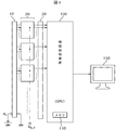
- FIG. 4 attached is an X-ray analyzer when the semiconductor X-ray detector according to the present invention including the semiconductor X-ray sensor unit 10, the readout unit 20, and the wiring unit 30 described above is employed.
- the entire circuit configuration is shown. That is, as is clear from the figure, detection signals from a large number of X-ray sensors (cells) constituting the semiconductor X-ray sensor unit 10 (that is, signals from the detection electrodes 14) are arranged on the back surface thereof.
- a reading unit 20 constituted by a plurality of (eight) reading units 22 and subjected to predetermined processing in a processing circuit formed in a large number by the ASIC, for example, via the wiring unit 30, for example.
- Various analysis processes are executed based on the information of the diffracted X-rays input to the information processing apparatus 100 including the CPU, and the results are displayed on the display unit (display device) 150. To do.
- each X-ray sensor determined by the combination of the eight readout units 22 is used.
- the position (coordinates) of the (cell) on the XY plane is stored in the memory 110 or the like provided therein.
- each detection signal from the semiconductor X-ray sensor unit 10 is subjected to predetermined processing. That is, a detection signal from the detection electrode 14 that is an output terminal of each X-ray sensor (cell) is generated by a circuit formed by an ASIC in a plurality of (eight) read units 22 constituting the read unit 20, for example, Amplification processing, waveform shaping processing, comparison processing, and counting processing are performed and can be extracted as a signal indicating the intensity of incident X-rays. It would be preferable to provide an X-ray diffractometer.
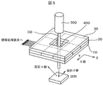
- FIG. 5 attached here shows an example of diffracted X-ray detection when an X-ray diffractometer that detects diffracted X-rays from a sample is configured by using the semiconductor X-ray detector described above. That is, the X-ray generated by the small X-ray tube 300 and passing through the incident optical system 350 such as a collimator is integrally laminated by, for example, the semiconductor X-ray sensor unit 10, the reading unit 20, and the wiring unit 30. The sample is irradiated vertically through a through hole 400 (formed by the openings 11, 21, and 31) formed in the center of the X-ray detector.
- a through hole 400 formed by the openings 11, 21, and 31
- the intensity of the diffracted X-rays generated from the sample is detected by the semiconductor X-ray sensor unit 10, the reading unit 20, and the wiring unit 30 that constitute the X-ray detector.
- the X-ray detector according to the present invention is easy to miniaturize and is suitable for a detector having a relatively short optical distance. It is also possible to provide a handheld X-ray diffractometer or the like.
- FIG. 6 attached shows a modified example of the semiconductor X-ray detector described above.
- the number of readout units 22 constituting the readout unit 20 is increased corresponding to a larger semiconductor X-ray sensor unit 10, and here, an example in which 24 units are combined. Indicates.
- illustration of the wiring portion 30 is omitted for simplicity of explanation.
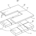
- FIG. 7 attached as another modification, the shape of the semiconductor X-ray sensor unit 10 and the reading unit 20 described above is changed to the above-mentioned “B” shape, and the “U” shape is used. It shows what was made.
- the shape of the semiconductor X-ray sensor unit 10 and the reading unit 20 described above is changed to the above-mentioned “B” shape, and the “U” shape is used. It shows what was made.
- FIG. 8 attached herewith shows an example in which a plurality of (16) rectangular readout units 22 are combined in place of the substantially square readout unit.
- the shapes of the semiconductor X-ray sensor unit 10 and the reading unit 20 do not match.
- FIG. 9 attached illustrates an example in which a plurality of (12) rectangular readout units 22 are combined with the disk-shaped semiconductor X-ray sensor unit 10. The shapes of the semiconductor X-ray sensor unit 10 and the reading unit 20 do not match.
- information indicating that the corresponding X-ray sensor (cell) does not exist is input (stored) in advance to the memory 110 or the like constituting the information processing apparatus 100.
- the same X-ray detection function as described above can be obtained.
- the number of X-ray sensors is substantially equal to the total number of processing circuit units formed inside the readout unit constituted by a plurality of readout units.
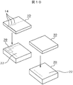
- a semiconductor X-ray sensor unit 10 and a readout unit 22 formed in the same shape are prepared, These are stacked and formed integrally.
- An X-ray detector provided with an opening (through hole) or a notch in the central portion in the same manner as described above by combining a plurality of these integrally formed as appropriate. Can be configured.
- the X-ray detector according to the present invention has an opening (through hole) at the center, and can detect diffracted X-rays radiated from the sample in a ring shape around it.
- a semiconductor X-ray sensor unit 10 having a large number of X-ray sensors (cells) in its interior (in this example, “B” or “U” shape) and on the back surface thereof.
- Each of which is formed in a rectangular shape, and a plurality of processing units, which are so-called ASICs, in which a large number of processing circuits are formed by three-dimensional mounting, are combined to form a shape of the semiconductor X-ray sensor unit 10.
- the reading sections 20 formed identically or correspondingly are stacked and attached together.
- a large number of processing circuits can be formed in the readout unit 20 corresponding to the large number of X-ray sensors (cells) of the semiconductor X-ray sensor unit 10, and the output terminal can be connected to Si. It is structured to be taken out to the back surface of the reading unit 20 through a via.
- a plurality of readout units 22 made of ASIC are appropriately combined in accordance with the shape of the semiconductor X-ray sensor unit 10 so that an opening (through hole) is formed at the center.
- the readout unit corresponding to the semiconductor X-ray sensor equipped with () can be easily configured.
- a desired shape can be freely set without any limitation on the combination shape and the number of the reading units depending on the arrangement of the output terminals. It can be assembled into a shape.
- the output terminals can be easily taken out from the back surface. For this reason, it is possible to configure a desired shape by combining a plurality of units.
- an opening is formed at the center of the unit, and the configuration is suitable for detecting diffracted X-rays at a short distance.
- a semiconductor X-ray detector capable of satisfying the above will be provided.
- SYMBOLS 10 Semiconductor X-ray sensor part, 11 ... Opening part (hole), 12 ... X-ray detection part, 13 ... Bias electrode, 14 ... Detection electrode, 20 ... Reading part, 21 ... Opening part (hole), 22 ... Reading unit , 2211 ... pad, 2212 ... amplifier, 2213 ... waveform shaping circuit, ... 2222 ... comparison circuit, 2232 ... counting circuit, 2214, 2223, 2225, 2233, 2234, 2241, 2242 ... Si through via, 2200 ... pad, 30 ... wiring part.
Landscapes
- Physics & Mathematics (AREA)
- Health & Medical Sciences (AREA)
- Life Sciences & Earth Sciences (AREA)
- General Physics & Mathematics (AREA)
- High Energy & Nuclear Physics (AREA)
- Molecular Biology (AREA)
- Spectroscopy & Molecular Physics (AREA)
- Measurement Of Radiation (AREA)
Abstract
半導体X線検出器は、略中央部に開口部11を有し、内部に多数のピクセル状のX線センサを形成した半導体X線センサ部10と、当該半導体X線センサ部の裏面に配置され、複数のX線センサから出力される信号の各々に所定の処理を行って検出信号を出力する読み出し部20とを備える。読み出し部は、複数の読み出しユニット22を平面状に一体に組み立てて構成され、各読み出しユニットは、それぞれ、矩形形状に形成され、表面に複数パッドを形成し、内部に複数の処理回路部や貫通ビアを備え、裏面に複数のパッドを備える。半導体X線センサ部と読み出し部は、積層して一体に形成される。
Description
本発明は、各種分析において使用されるX線の検出を行う半導体X線検出器に関し、特に、試料からの回折X線を検出するのに適した新規な構造の半導体X線検出器に関する。
X線を利用した各種試料の分析は、試料の分解を伴わず、所謂、非破壊分析として広い分野において採用されている。従来、例えば、以下の特許文献1によれば、X線発生装置と二次元(エリア)X線検出器を搭載した、可搬なハンドヘルド型のX線回折計が既に知られている。
一方、回折X線などの強度を検出するためには、一般に、感光フィルムなどのイメージングプレート(IP)が利用されてきたが、しかしながら、近年における半導体製造技術の著しい発展に伴い、各種の半導体によるX線検出器が開発されている。例えば、以下の特許文献2には、複数のピクセルを具備した光子カウントモード(PCM)検出器であって、カドミウム亜鉛テルライド(CZT)検出器と、一又は複数の読み出し回路を実装したASICチップとを組み合わせたものが既に開示されている。また、以下の特許文献3には、かかるピクセル(画素)を複数備えた装置において、当該画素により収集される線量をモニタリングする方法やそのためのX線検出装置も既に知られている。また、以下の特許文献4によれば、半導体X線アレイ検出器を利用したX線撮像装置も既に知られている。
更には、以下の特許文献4には、検出器のコンパクト化と、そして、複数の単位画素検出器を並べた場合におけるデッドスペースの発生をなくした構造が既に開示されている。
しかしならが、上述した従来技術によれば、以下のような問題点がある。即ち、試料からのX線、特に、回折X線を検出する場合、X線は、三次元空間内において、試料を中心として同心円上に回折される。そのことから、かかる回折X線を検出するためには、半導体X線検出器も、従来のイメージングプレートなどと同様に、平面(二次元)的に広がる検出領域を備える必要がある。しかしながら、上記従来技術の検出器では、その構造や製造技術から、十分に大きなサイズの検出領域を確保することは難しく、そのため、例えば、上記特許文献1のX線回折計では、複数の一次元(リニア)センサ又は二次元(エリア)センサを組み合わせて使用すること、即ち、分散して配置された複数の半導体X線検出装置により、かかる回折X線を、個別に検出し、その後の処理において、これらを関連付けることにより分析を行っていた。そのため、精度の高い回折X線の分析は困難であった。
また、上記特許文献2~特許文献4にも開示されるように、半導体X線検出器では、特に、ASICを含むアレイ構造における配線部、特に、基板の表面上に配置される構造をその理由として、これらX線検出素子を所望の数だけ組み合わせて所望の形状のX線検出器とすることは困難であった。
なお、上記特許文献5では、複数の単位画素検出器を並べた場合におけるデッドスペースの発生をなくすことを目的として、各素子をその配線部である引き出しパッド部が外側に配列されるように、複数の検出素子を、二列に、配置している。しかしながら、かかる配置・構造では、検出素子を二列以上に亘って配置した場合には、デッドスペースが発生してしまい、やはり、検出器を所望の数だけ組み合わせて所望の形状のX線検出器とすることは困難であった。
そこで、本発明は、上述した従来技術における問題点に鑑みて達成されたものであり、即ち、複数のユニットを組み合わせることにより所望の形状に構成することが可能な半導体X線検出素子を、特に、その中央部に開口部を形成して近距離での回折X線の検出に好適な形状に構成することが可能な、新たな構成の半導体X線検出器を提供することをその目的とする。
まず、本発明によれば、上記の目的を達成するため、少なくとも略中央部に開口部を有する板状の外形を有し、その表面と裏面との間に複数のピクセル状のX線センサを形成した半導体X線センサ部と、前記半導体X線センサ部の裏面に配置され、当該半導体X線センサ部を構成する複数のX線センサから出力される信号の各々に所定の処理を行って検出信号を出力する読み出し部と、を備えた半導体X線検出器であって、前記読み出し部は、各々、板状の矩形形状に形成され、表面に複数の入力部を形成すると共に、その内部に複数の処理回路部と複数の貫通ビアとを備え、かつ、裏面に複数の出力端子を備えた読み出しユニットを、複数、平面状に一体に組み立てて構成されており、かつ、当該半導体X線センサ部と当該読み出し部とを積層して一体に形成した半導体X線検出器が提供される。
また、本発明では、前記に記載した半導体X線検出器において、前記半導体X線センサ部は、中央部に開口を有すると共に、その外形を、「ロ」の字状、「コ」の字状、又は、円形に形成されていることが好ましく、又は、前記半導体X線センサ部を構成する複数のピクセル状のX線センサの数は、前記複数の読み出しユニットにより構成された前記読み出し部の内部に形成された処理回路部の総数にほぼ等しいことが好ましい。そして、前記読み出し部を構成する前記複数の読み出しユニットの各々を、その内部に前記複数の処理回路部を3次元的に形成したASICにより構成することが、又は、前記読み出し部から出力される検出信号は、入射X線の強度信号であることが好ましい。
また、本発明によれば、やはり上記の目的を達成するため、少なくとも略中央部に開口部を有する板状の外形を有し、その表面と裏面との間に複数のピクセル状のX線センサを形成した半導体X線センサ部と、前記半導体X線センサ部の裏面に配置され、当該半導体X線センサ部を構成する複数のX線センサから出力される信号の各々に所定の処理を行って検出信号を出力する読み出し部と、を備えた半導体X線検出器であって、前記読み出し部は、各々、板状の矩形形状に形成され、表面に複数の入力部を形成すると共に、その内部に複数の処理回路部と複数の貫通ビアとを備え、かつ、裏面に複数の出力端子を備えた、複数の読み出しユニットから構成されており、前記半導体X線センサ部は、前記読み出し部を構成する読み出しユニットの各々の表面に積層されて一体に形成されており、そして、前記読み出しユニットとその表面に一体に積層された前記半導体X線センサ部を単位として、複数を平面状に一体に組み立てられている半導体X線検出器が提供される。
上述した本発明によれば、所望の形状に構成することが可能な半導体X線検出素子であって、特に、その中央部に開口部を形成して近距離での回折X線の検出に好適な形状に構成することが可能な半導体X線検出器を容易に提供することが可能となるという極めて優れた効果を発揮する。
以下、本発明の実施の形態になる半導体X線検出器について、添付の図面を参照しながら詳細に説明する。
まず、添付の図1は、本発明になるX線検出器の全体構成を示す。この図において、符号10は、例えば、CdTe、CdZnTe、その他の、所謂、半導体X線センサ部を示しており、以下にも詳述するように、半導体により外形略正方形状に形成され、かつ、その中央部に開口部(穴)11を設けたX線検出部12を有する。そして、当該X線検出部12の一方の面(図の上面側)には、負の電位を印加するバイアス電極13を、例えば、ITO(Indium Tin Oxide)等の透明材料により形成すると共に、他方の面(図の下面側)には、所謂、X線のエネルギーによって発生する電子を検出するための検出電極14、14…が、多数のX線センサが、ピクセル状に形成されている。即ち、この半導体X線センサ部10では、半導体からなるX線検出部12を挟んで配置されたバイアス電極13と検出電極14により、多数のピクセル状のX線センサ(セル)が形成され、アレイ状に並んで配置されている。なお、図のように、この半導体センサ部10を中空形状に形成することによれば、以下にも詳述するが、特に、試料から発生するリング状の回折X線の強度を検出することにおいて、優れた効果を発揮することが出来る。
次に、上述した半導体X線センサ部10の下面には、同様の形状をした(即ち、外形略正方形状であり、かつ、その中央部に開口部(穴)21を設けた)読み出し部20が設けられている。この読み出し部20は、図からも明らかなように、複数の部分(読み出しユニット22、22…:なお、本例では8個)を組み合わせることにより構成されており、そして、それぞれ、所謂、ASIC(Application Specific Integrated Circuit)により、Si貫通ビア(シリコン製半導体チップの内部に垂直に貫通する電極)などにより、種々の回路が3次元的に構成されている。また、その表面には、多数の、読出し部23、23…が、上記半導体X線センサ部10の検出電極14、14…に対応する位置に形成されている。そして、この読み出し20の下方には、更に、同様の形状をした(即ち、外形略正方形状であり、かつ、その中央部に開口部(穴)31を設けた)例えば、ワイヤボンディングパッドからなる配線部30が設けられ、当該配線部30の一部(本例では、側壁部)に設けた端子部32を介して、上記多数のX線センサ(検出電極14、14…)からの出力が出力されると共に、後にも述べる必要な各種の電圧が、上記読み出し部20を介して、半導体X線センサ部10へ供給される。
次に、添付の図2には、上記ASICからなる読み出し部20、特に、読み出し部を構成する読み出しユニット22の詳細が、上記半導体X線センサ部10を構成するX線センサ(セル)の詳細と共に示されている。
まず、X線センサ(セル)は、上述したように、X線検出部12とそれを挟んで配置されたバイアス電極13と検出電極14により構成されている。なお、この図において、符号15は、上記X線検出部12の下面に形成された絶縁層を示しており、この図からも明らかなように、上記検出電極14は、この絶縁層15を介して形成されており、その下端部がパッド状になっている。また、上記半導体X線センサ部10の下面の一部には、上記の検出電極と同様にして、アース電極16が形成されると共に、更に、上記バイアス電極13にバイアス電圧(負の電圧:-VB)を導くためのバイアス端子17が、絶縁層を介して内部に導電材を充填した、所謂、Si貫通ビアとして形成されており、かつ、その下端部はパッド状になっている。
そして、ASICからなる読み出し部ユニット22は、本例では、例えば、4層の基板により構成されており、かつ、図からも明らかなように、これら4層の基板のそれぞれには、以下に述べる読み出し回路が形成され、そして、積層されて一体に形成されている。
まず、図において、最上部の第一層221の表面には、図に破線で示すように、上記半導体X線センサ部10の検出電極14の位置に対応して、即ち、検出信号の入力端子としてのパッド2211が形成されると共に、上記X線検出部12に対応する位置には、検出される信号を所望の振幅に増幅するための増幅器2212と、当該増幅された信号の波形を整形するための波形整形回路2213が設けられている。そして、当該波形整形回路2213の出力は、更に、他のSi貫通ビア2214に接続されている。また、図の符号2201は、上記アース電極16のパッドに対応して形成されたSi貫通ビアを、そして、符号2202は、上記バイアス端子16のパッドに対応して形成されたSi貫通ビアを、それぞれ、示している。
次に、第二層222の表面には、上記第一層221のSi貫通ビア2214に対応してパッド2221が設けられ、そして、比較回路2222が形成され、その出力端には、Si貫通ビア2223が設けられている。また、第二層222の表面には抵抗2224が形成され、その一端は上記比較回路2222の一方の入力に接続されると共に、その他端は、比較参照電圧VRefに接続されるSi貫通ビア2225に接続されている。また、上記第一層221のSi貫通ビア2201、2202に対応する位置にも、やはり同様に、Si貫通ビア2201、2202が形成されている。
更に、第三層223の表面には、上記第二層222のSi貫通ビア2223に対応する位置にはパッド2231が形成されると共に、更に、計数回路2232が形成されており、その出力はSi貫通ビア2233へ接続されている。また、上記第二層222に形成したSi貫通ビア2225に対応する位置にも、Si貫通ビア2234が形成されており。そして、この第三層223にも、やはり、上記第二層のSi貫通ビア2201、2202に対応する位置には、Si貫通ビア2201、2202が形成されている。
最後に、第四層(基板)224には、上記第三層223のSi貫通ビア2233に対応する位置に、更には、上記比較参照電圧VRefが接続されるSi貫通ビア2225の位置に対応して、それぞれ、Si貫通ビア2241、2242が設けられており、その下端部(即ち、第三層223の裏面)には、それぞれ、パッドが形成されている。また、同様に、この第四層(基板)224にも、Si貫通ビア2201、2202が形成されると共に、その下端部には、それぞれ、出力端子としてパッドが形成されている。
そして、上述した半導体X線センサ部10を、上記の第一層221から第四層224を一体に積層してなる読み出しユニット22を複数(図1の例では8枚)平面状に組み合わせて形成した読み出し部20の表面に配置することによれば、その表面にアレイ状に並んで配置された多数のピクセル状のX線センサ(セル)からの出力、即ち、検出電極14、14…からの信号は、読み出し部20を構成する複数(8個)の読み出しユニット22の内部に形成された読み出し回路において、それぞれ、所定の処理が施され、その下面に設けられた多数の端子であるパッドを介して取り出されることとなる。また、上記半導体X線センサ部10を駆動するために必要なバイアス電極13へのバイアス電圧-VBの印加や、アース電極16の接地も同様に、読み出しユニット22の一部に形成されたSi貫通ビア2201、2202を介して行なわれることとなる。
なお、上述したみ読み出しユニット22を8枚、一体に組み立てて構成された読み出し部20を、裏面から見た様子が、添付の図3に示されている。この図からも明らかなように、当該8枚の読み出しユニット22を、平面状に、一体に組み立てて形成された読み出し部20の裏面には、各読み出しユニット22の内部に形成された読み出し回路の数を合計した数の、即ち、上記半導体X線センサ部10を構成するX線センサ(セル)の数(実際には、更に、必要なバイアス電極13へのバイアス電圧-VBの印加や、アース電極16の接地、更には、比較参照電圧VRefの供給に必要なSi貫通ビア2201、2202、2242の下端に形成されたパッドの数をも含む数)のパッド2200が、配列されることとなる。
そして、上述した読み出し部20から上記多数のパッド2200を介して出力された出力(即ち、上記半導体X線センサ部10の各X線センサ(セル)の検出電極14からの信号)は、更に、上記ワイヤボンディングパッドからなる配線部30に導かれ、更には、ここでは図示しないが、その内部に設けられた、例えば、パラレル/シリアル変換器、又は、チャネルスイッチ、マルチプレクサ等によりその出力数を低減して、その側壁部に設けられた端子部32を介して出力される。
続いて、添付の図4は、上述した半導体X線センサ部10、読み出し部20、更には、配線部30を含む、本発明になる半導体X線検出器を採用した場合の、X線分析装置全体の回路構成を示す。即ち、図からも明らかなように、上記半導体X線センサ部10を構成する多数のX線センサ(セル)からの検出信号(即ち、検出電極14からの信号)は、その裏面に配置された複数(8枚)の読み出しユニット22から構成された読み出し部20に導かれ、ASICによりその内部に多数形成された処理回路において所定の処理が施された後、配線部30を介して、例えば、CPUを含んで構成される情報処理装置100に入力され、得られた回折X線の情報により、各種の解析処理を実行し、更には、その結果を、表示部(ディスプレイ装置)150上に表示する。
そして、情報処理装置100では、上記半導体X線センサ部10を構成する多数のX線センサ(セル)からの検出信号を処理する場合、上記8枚の読み出しユニット22の組み合わせにより定まる各X線センサ(セル)のXY平面上の位置(座標)を、その内部に設けたメモリ110等に予め記憶しておくことにより、当該XY平面上の多数の検出位置にける正確な入射X線の検出が可能となる。
更に、本発明になる半導体X線検出器によれば、特に、上述した読み出し部20によれば、上記半導体X線センサ部10からの検出信号には、各々、所定の処理が施される。即ち、各X線センサ(セル)の出力端子である検出電極14からの検出信号は、読み出し部20を構成する複数(8枚)の読み出しユニット22内にASICにより形成された回路により、例えば、増幅処理、波形整形処理、比較処理、計数処理が行われており、入射X線の強度を示す信号として取り出すことが可能であることから、特に、回折X線を利用して試料の特性を測定する、X線回折装置に提供することが好ましいであろう。
添付の図5には、上述した半導体X線検出器を利用することにより、試料からの回折X線を検出するX線回折装置を構成した場合における、回折X線検出の一例を示す。即ち、小型X線管球300により発生し、コリメータ等の入射光学系350を通したX線を、例えば、半導体X線センサ部10、読み出し部20、そして、配線部30を一体に積層してなるX線検出器の中央部に形成された貫通穴400(開口部11、21、31により形成)と介して試料に垂直に照射する。これにより当該試料から発生する回折X線をX線検出器を構成する半導体X線センサ部10、読み出し部20、そして、配線部30により、その強度を検出する。この図からも明らかなように、本発明になるX線検出器は、小型化が容易であり、かつ、その光学距離が比較的に短い検出器において好適であることから、特に、可搬なハンドヘルド型のX線回折計などに提供することも可能である。
更に、添付の図6には、上述した半導体X線検出器の変形例を示す。この例では、例えば、より大型の半導体X線センサ部10に対応して、上記読み出し部20を構成する読み出しユニット22の枚数を増大したものであり、ここでは、24枚のユニットを組み合わせた例を示す。なお、ここでは、説明の簡単のため、配線部30については、その図示を省略する。
また、添付の図7には、更に他の変形例として、上述した半導体X線センサ部10と読み出し部20の形状を、上記の「ロ」の字状に代えて、「コ」の字状にしたものを示している。なお、この例では、その中央の開口部11、21に代わる切り欠き部11’、21’を介して、X線管球300により発生したX線を試料の表面に照射することは、当業者であれば明らかであろう。
加えて、添付の図8には、上記の略正方形状の読み出しユニットに代え、長方形状の読み出しユニット22を、複数枚(16枚)、組み合わせた例を示している。なお、この例では、半導体X線センサ部10と読み出し部20の形状が一致していない。更に、添付の図9には、円盤状の半導体X線センサ部10に対して、矩形状の読み出しユニット22を、複数枚(12枚)、組み合わせた例を示しており、この場合においても、半導体X線センサ部10と読み出し部20の形状が一致していない。しかしながら、かかる場合においても、上述したように、上記情報処理装置100を構成するメモリ110等に対して、対応するX線センサ(セル)が存在しない旨の情報を予め入力(格納)しておくことによれば、上記と同様のX線の検出機能が得られることは明らかであろう。なお、この場合には、出来る限り、複数の読み出しユニットを、上記半導体X線センサ部の形状に合わせるように配置することが、換言すれば、半導体X線センサ部を構成する複数のピクセル状のX線センサの数が、複数の読み出しユニットにより構成された前記読み出し部の内部に形成された処理回路部の総数にほぼ等しくなるようにすることが好ましい。
あるいは、上述した実施例に代えて、添付の図10に示すように、互いに同一の形状(本例では、矩形)に形成した半導体X線センサ部10と読み出しユニット22とを用意し、予め、これらを重ねて一体に形成する。そして、この一体に形成したものを単位として、これらを複数、適宜、組み合わせることによっても、上記と同様にして、中央部に開口部(貫通穴)又は、切り欠き部を備えたX線検出器を構成することが出来る。
以上の説明からも明らかなように、本発明になるX線検出器では、その中央部に開口部(貫通穴)を備え、その周辺に、試料からリング状に放射する回折X線を検出可能な形状(本例では「ロ」又は「コ」の字状)に形成され、かつ、その内部に多数のX線センサ(セル)を備えた半導体X線センサ部10を備えると共に、その裏面には、各々、矩形に形成され、その内部に3次元実装により多数の処理回路を形成した、所謂、ASICである読み出しユニット22を、複数枚、組み合わせることにより、上記半導体X線センサ部10の形状に同一に又は対応して形成された読み出し部20が積層され、一体に取り付けられている。その結果、上記半導体X線センサ部10の多数のX線センサ(セル)に対応して、その処理回路を、当該読み出し部20内に多数形成することが出来ると共に、その出力端子を、Si貫通ビアを介して、読み出し部20の裏面に取り出す構造としている。
そして、上述した構成によれば、ASICにより構成された読み出しユニット22を、上記半導体X線センサ部10の形状に合わせて、複数枚、適宜、組み合わせることにより、その中央部に開口部(貫通穴)を備えた半導体X線センサに対応した読み出し部を、容易に構成することが出来る。その際、特に、その出力端子を読み出し部20の裏面から取り出すことによれば、当該出力端子の配置によって、複数の読み出しユニットの組み合わせ形状や枚数に制限が加えられることなく、自在に、所望の形状に組み立てることが可能となる。特に、複数の読み出しユニットの組み合わせた結果、その一部のユニットが、その周囲の四辺を他のユニットで取り囲まれても、その出力端子を、その裏面から容易に取り出すことが出来る。そのため、複数のユニットを組み合わせることにより所望の形状に構成することが可能であり、特に、その中央部に開口部を形成して近距離での回折X線の検出に好適な形状に構成することが可能な半導体X線検出器が提供されることとなる。
10…半導体X線センサ部、11…開口部(穴)、12…X線検出部、13…バイアス電極、14…検出電極、20…読み出し部、21…開口部(穴)、22…読み出しユニット、2211…パッド、2212…増幅器、2213…波形整形回路、…、2222…比較回路、2232…計数回路、2214、2223、2225、2233、2234、2241、2242…Si貫通ビア、2200…パッド、30…配線部。
Claims (6)
- 少なくとも略中央部に開口部を有する板状の外形を有し、その表面と裏面との間に複数のピクセル状のX線センサを形成した半導体X線センサ部と、
前記半導体X線センサ部の裏面に配置され、当該半導体X線センサ部を構成する複数のX線センサから出力される信号の各々に所定の処理を行って検出信号を出力する読み出し部と、
を備えた半導体X線検出器であって、
前記読み出し部は、各々、板状の矩形形状に形成され、表面に複数の入力部を形成すると共に、その内部に複数の処理回路部と複数の貫通ビアとを備え、かつ、裏面に複数の出力端子を備えた読み出しユニットを、複数、平面状に一体に組み立てて構成されており、かつ、当該半導体X線センサ部と当該読み出し部とを積層して一体に形成したことを特徴とする半導体X線検出器。 - 前記請求項1に記載した半導体X線検出器において、前記半導体X線センサ部は、中央部に開口を有すると共に、その外形を、「ロ」の字状、「コ」の字状、又は、円形に形成されていることを特徴とする半導体X線検出器。
- 前記請求項1に記載した半導体X線検出器において、前記半導体X線センサ部を構成する複数のピクセル状のX線センサの数は、前記複数の読み出しユニットにより構成された前記読み出し部の内部に形成された処理回路部の総数にほぼ等しいことを特徴とする半導体X線検出器。
- 前記請求項1に記載した半導体X線検出器において、前記読み出し部を構成する前記複数の読み出しユニットの各々を、その内部に前記複数の処理回路部を3次元的に形成したASICにより構成したことを特徴とする半導体X線検出器。
- 前記請求項1に記載した半導体X線検出器において、前記読み出し部から出力される検出信号は、入射X線の強度信号であることを特徴とする半導体X線検出器。
- 少なくとも略中央部に開口部を有する板状の外形を有し、その表面と裏面との間に複数のピクセル状のX線センサを形成した半導体X線センサ部と、
前記半導体X線センサ部の裏面に配置され、当該半導体X線センサ部を構成する複数のX線センサから出力される信号の各々に所定の処理を行って検出信号を出力する読み出し部と、
を備えた半導体X線検出器であって、
前記読み出し部は、各々、板状の矩形形状に形成され、表面に複数の入力部を形成すると共に、その内部に複数の処理回路部と複数の貫通ビアとを備え、かつ、裏面に複数の出力端子を備えた、複数の読み出しユニットから構成されており、
前記半導体X線センサ部は、前記読み出し部を構成する読み出しユニットの各々の表面に積層されて一体に形成されており、そして、
前記読み出しユニットとその表面に一体に積層された前記半導体X線センサ部を単位として、複数を平面状に一体に組み立てられていることを特徴とする半導体X線検出器。
Priority Applications (1)
| Application Number | Priority Date | Filing Date | Title |
|---|---|---|---|
| US13/812,559 US20130126745A1 (en) | 2010-07-30 | 2011-07-29 | Semiconductor x-ray detector |
Applications Claiming Priority (2)
| Application Number | Priority Date | Filing Date | Title |
|---|---|---|---|
| JP2010172597A JP5457971B2 (ja) | 2010-07-30 | 2010-07-30 | 半導体x線検出器 |
| JP2010-172597 | 2010-07-30 |
Publications (1)
| Publication Number | Publication Date |
|---|---|
| WO2012015045A1 true WO2012015045A1 (ja) | 2012-02-02 |
Family
ID=45530244
Family Applications (1)
| Application Number | Title | Priority Date | Filing Date |
|---|---|---|---|
| PCT/JP2011/067515 Ceased WO2012015045A1 (ja) | 2010-07-30 | 2011-07-29 | 半導体x線検出器 |
Country Status (3)
| Country | Link |
|---|---|
| US (1) | US20130126745A1 (ja) |
| JP (1) | JP5457971B2 (ja) |
| WO (1) | WO2012015045A1 (ja) |
Citations (2)
| Publication number | Priority date | Publication date | Assignee | Title |
|---|---|---|---|---|
| JP2005043263A (ja) * | 2003-07-23 | 2005-02-17 | Okutekku:Kk | 信号検出器 |
| JP2009074964A (ja) * | 2007-09-21 | 2009-04-09 | Kyocera Corp | X線検出素子搭載用配線基板およびx線検出装置 |
Family Cites Families (5)
| Publication number | Priority date | Publication date | Assignee | Title |
|---|---|---|---|---|
| GB0019451D0 (en) * | 2000-08-09 | 2000-09-27 | Secr Defence | Imaging apparatus |
| US20100074396A1 (en) * | 2008-07-07 | 2010-03-25 | Siemens Medical Solutions Usa, Inc. | Medical imaging with black silicon photodetector |
| US7822177B2 (en) * | 2008-12-04 | 2010-10-26 | Multiwire Laboratories, Ltd. | Back-reflection X-ray crystallography method and system |
| US8033724B2 (en) * | 2009-06-30 | 2011-10-11 | The Boeing Company | Rapid assembly and operation of an X-ray imaging system |
| JP5672693B2 (ja) * | 2009-10-07 | 2015-02-18 | 富士通株式会社 | X線分析方法 |
-
2010
- 2010-07-30 JP JP2010172597A patent/JP5457971B2/ja active Active
-
2011
- 2011-07-29 US US13/812,559 patent/US20130126745A1/en not_active Abandoned
- 2011-07-29 WO PCT/JP2011/067515 patent/WO2012015045A1/ja not_active Ceased
Patent Citations (2)
| Publication number | Priority date | Publication date | Assignee | Title |
|---|---|---|---|---|
| JP2005043263A (ja) * | 2003-07-23 | 2005-02-17 | Okutekku:Kk | 信号検出器 |
| JP2009074964A (ja) * | 2007-09-21 | 2009-04-09 | Kyocera Corp | X線検出素子搭載用配線基板およびx線検出装置 |
Also Published As
| Publication number | Publication date |
|---|---|
| JP5457971B2 (ja) | 2014-04-02 |
| US20130126745A1 (en) | 2013-05-23 |
| JP2012032292A (ja) | 2012-02-16 |
Similar Documents
| Publication | Publication Date | Title |
|---|---|---|
| US8063380B2 (en) | Semiconductor crystal high resolution imager | |
| US10483316B2 (en) | Fabrication and operation of multi-function flexible radiation detection systems | |
| US6841784B2 (en) | Radiation sensor device | |
| AU2002218600B2 (en) | Detection of radiation and positron emission tomography | |
| WO2013012809A1 (en) | Radiation detector modules based on multi-layer cross strip semiconductor detectors | |
| US9993894B1 (en) | Compact radiation detector | |
| US20120181438A1 (en) | Radiation detecting apparatus, radiation detecting system, and method of manufacturing radiation detecting apparatus | |
| AU2002218600A1 (en) | Detection of radiation and positron emission tomography | |
| JP2009198343A (ja) | 検出器配列基板およびこれを用いた核医学診断装置 | |
| US10976450B2 (en) | Combined scintillation crystal, combined scintillation detector and radiation detection device | |
| JP5560338B2 (ja) | X線応力測定装置 | |
| US7138632B2 (en) | Radiation detector | |
| JPH11281747A (ja) | 放射線半導体検出器 | |
| JP4934826B2 (ja) | 放射線画像検出モジュールおよび放射線画像検出装置 | |
| RS57333B1 (sr) | Struktura za čitanje naelektrisanja, namenjena za detekciju fotona ili čestica | |
| JP5457971B2 (ja) | 半導体x線検出器 | |
| JP5136736B2 (ja) | 放射線画像検出モジュールおよび放射線画像検出装置 | |
| CN219328903U (zh) | 像素型面阵探测器伽马能谱测试系统 | |
| JP2015141037A (ja) | 放射線検出器 | |
| US20080258072A1 (en) | Detector for Ionizing Radiation | |
| JP2009074817A (ja) | 半導体検出器モジュール、および該半導体検出器モジュールを用いた放射線検出装置または核医学診断装置 | |
| Tojo et al. | Development of a novel silicon stripixel detector for RHIC-PHENIX detector upgrade | |
| JP2022101063A (ja) | X線検出装置 | |
| JP4545628B2 (ja) | 放射線検出回路、放射線検出器および放射線検査装置 | |
| JP2005121528A (ja) | 2次元イメージ素子及びそれを利用した2次元イメージ検出装置並びにx線分析装置 |
Legal Events
| Date | Code | Title | Description |
|---|---|---|---|
| 121 | Ep: the epo has been informed by wipo that ep was designated in this application |
Ref document number: 11812634 Country of ref document: EP Kind code of ref document: A1 |
|
| WWE | Wipo information: entry into national phase |
Ref document number: 13812559 Country of ref document: US |
|
| NENP | Non-entry into the national phase |
Ref country code: DE |
|
| 122 | Ep: pct application non-entry in european phase |
Ref document number: 11812634 Country of ref document: EP Kind code of ref document: A1 |