WO2012014464A1 - 離散時間アナログ回路及びそれを用いた受信機 - Google Patents
離散時間アナログ回路及びそれを用いた受信機 Download PDFInfo
- Publication number
- WO2012014464A1 WO2012014464A1 PCT/JP2011/004239 JP2011004239W WO2012014464A1 WO 2012014464 A1 WO2012014464 A1 WO 2012014464A1 JP 2011004239 W JP2011004239 W JP 2011004239W WO 2012014464 A1 WO2012014464 A1 WO 2012014464A1
- Authority
- WO
- WIPO (PCT)
- Prior art keywords
- circuit
- discrete
- charge
- time analog
- holding means
- Prior art date
- Legal status (The legal status is an assumption and is not a legal conclusion. Google has not performed a legal analysis and makes no representation as to the accuracy of the status listed.)
- Ceased
Links
Images














Classifications
-
- H—ELECTRICITY
- H03—ELECTRONIC CIRCUITRY
- H03H—IMPEDANCE NETWORKS, e.g. RESONANT CIRCUITS; RESONATORS
- H03H15/00—Transversal filters
-
- H—ELECTRICITY
- H03—ELECTRONIC CIRCUITRY
- H03M—CODING; DECODING; CODE CONVERSION IN GENERAL
- H03M1/00—Analogue/digital conversion; Digital/analogue conversion
- H03M1/12—Analogue/digital converters
- H03M1/18—Automatic control for modifying the range of signals the converter can handle, e.g. gain ranging
-
- H—ELECTRICITY
- H03—ELECTRONIC CIRCUITRY
- H03H—IMPEDANCE NETWORKS, e.g. RESONANT CIRCUITS; RESONATORS
- H03H19/00—Networks using time-varying elements, e.g. N-path filters
- H03H19/004—Switched capacitor networks
-
- H—ELECTRICITY
- H03—ELECTRONIC CIRCUITRY
- H03M—CODING; DECODING; CODE CONVERSION IN GENERAL
- H03M1/00—Analogue/digital conversion; Digital/analogue conversion
- H03M1/12—Analogue/digital converters
- H03M1/50—Analogue/digital converters with intermediate conversion to time interval
Definitions
- the present invention relates to a discrete-time analog circuit and a receiver using the same, and more particularly to a technique for performing reception signal processing such as frequency conversion and filter processing by discrete-time analog processing.
- Patent Document 1 In order to achieve downsizing, low power consumption, and integration of analog signal processing units and digital signal processing units, wireless receivers are known to receive and process high-frequency signals directly in discrete time.
- Patent Document 1 For example, Patent Document 1 and Non-Patent Document 1).
- FIG. 1 is a diagram showing an overall configuration of a direct sampling circuit disclosed in Patent Document 1.
- FIG. 2 is a timing chart showing control signals input to the circuit of FIG.
- the direct sampling circuit in FIG. 1 converts the frequency of a received analog RF (Radio Frequency) signal into a discrete-time analog signal.
- the frequency conversion at this time uses a multi-tap direct sampling mixer (Multi-Tap Direct Sampling Mixer). More specifically, a filter characteristic that is a product of an FIR (Finite Impulse Response) filter and an IIR (Infinite Impulse Response) filter is realized by charge transfer between a plurality of capacitors included in the circuit of FIG.
- the characteristics near the passband are determined by the secondary IIR filter characteristics.
- FIG. 3A shows a wideband frequency characteristic
- FIG. 3B shows an example of a narrowband frequency characteristic near the passband.
- FIG. 4 is a diagram showing an overall configuration of the direct sampling circuit disclosed in Non-Patent Document 2.
- FIG. 5 is a timing chart showing control signals input to the circuit of FIG.
- the direct sampling circuit having the configuration as shown in FIG. 4 can realize a filter characteristic with a complex pole on the transfer function and a flat passband.
- this configuration as shown in the equation (1), only a value smaller than 1 can be selected as a filter coefficient, so that the range of poles that can be realized is narrowed, and the frequency characteristics can be raised by the poles at a low frequency. difficult.
- Decimation is required to achieve wideband filter characteristics. However, since a filter using decimation causes aliasing at a frequency corresponding to the decimation ratio, it is difficult to easily use a filter having the filter characteristics.
- the coefficient realization range is limited, so that the flattest characteristics and Chebyshev characteristics that are generally used in analog and digital filter design can be realized at any sampling frequency. There wasn't.
- the present invention has been made in view of such points, and an object of the present invention is to provide a discrete time analog circuit and a receiver having a wide band and steep filter characteristics with a high degree of freedom in setting positions of the zeros and poles of the filter.
- One aspect of the discrete-time analog circuit of the present invention includes a rotating capacitor circuit, a potential holding unit that is connected to an input line of the rotating capacitor circuit and amplifies an input potential or an input charge, and is arranged in series with the potential holding unit And at least one coefficient circuit having n charge holding units arranged in parallel to each other, and of the n charge holding units, the first charge holding unit connected to the potential holding unit and charged. And a pair of second charge holding means connected to the input line without passing through the potential holding means and sharing the charge of the rotate capacitor circuit or holding the potential in the rotate capacitor circuit. Circuit connection switching means.
- One aspect of the discrete-time analog circuit of the present invention includes a rotating capacitor circuit, a potential holding unit that is connected to an output line of the rotating capacitor circuit and amplifies an output potential or output charge, and is arranged in series with the potential holding unit And at least one coefficient circuit having n charge holding units arranged in parallel to each other, and of the n charge holding units, the first charge holding unit connected to the potential holding unit and charged. And a pair of second charge holding means connected to the output line without going through the potential holding means and sharing the charge of the rotating capacitor circuit or holding the potential in the rotating capacitor circuit. Circuit connection switching means.
- One aspect of the receiver of the present invention includes a discrete-time analog circuit described above, an antenna that receives an input signal, a signal received by the antenna, and outputs the amplified signal to the discrete-time analog circuit.
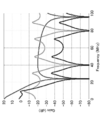
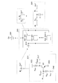
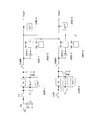
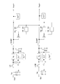
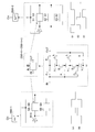
- Characteristic diagram showing an example of filter characteristics realized by the direct sampling circuit of the conventional configuration 2 1 is a block diagram showing a configuration of a direct sampling receiver according to Embodiment 1 of the present invention.
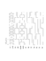
- FIG. 1 The figure which shows the clock (control signal) provided from a clock generation circuit Another configuration diagram of the discrete-time analog circuit according to the first embodiment The figure which shows the clock (control signal) provided from a clock generation circuit Another configuration diagram of the discrete-time analog circuit according to the first embodiment The figure for demonstrating operation
- FIG. 1 The figure which shows the common structure of the coefficient circuit which concerns on Embodiment 1.
- FIG. 10 is a characteristic diagram illustrating an example of filter characteristics realized by the discrete-time analog circuit according to the fifth embodiment.
- Configuration diagram of nth-order discrete-time analog circuit according to Embodiment 6 Another configuration diagram of the nth-order discrete-time analog circuit according to the sixth embodiment
- Configuration diagram of discrete-time analog circuit according to Embodiment 7 Another configuration diagram of the discrete-time analog circuit according to the seventh embodiment
- FIG. 10 is a characteristic diagram illustrating an example of filter characteristics realized by a discrete-time analog circuit according to the seventh embodiment.
- Configuration diagram of coefficient circuit according to Embodiment 8 Another configuration diagram of circuit connection according to the eighth embodiment Still another configuration diagram of circuit connection according to the eighth embodiment Still another configuration diagram of the coefficient circuit according to the ninth embodiment Configuration diagram of kth-order coefficient circuit according to Embodiment 9
- FIG. 7 is a block diagram showing a configuration of the direct sampling receiver according to the present embodiment.
- a direct sampling receiver 10 includes an antenna 11, a low noise amplifier (LNA) 12, a discrete time analog circuit 13, a reference frequency oscillating unit 14, and an A / D (Analog to Digital).
- a conversion processing unit 15 and a digital reception processing unit 16 are included.
- the direct sampling receiver 10 receives the electromagnetic wave 21 transmitted at the carrier frequency fRF , and performs frequency conversion and filter processing on the received signal in discrete time to extract a desired signal component.
- the direct sampling receiver 10 converts the extracted desired signal component into a digital signal, performs digital reception processing, and outputs the obtained reception data 27.
- the antenna 11 receives an electromagnetic wave 21 transmitted at a carrier frequency f RF from a transmission station (not shown), and converts it into an analog RF signal 22.
- the low noise amplifier 12 amplifies and outputs the analog RF signal 22.
- Discrete time analog circuit 13 receives amplified analog RF signal 23 and reference frequency signal 24 as inputs. Then, the discrete-time analog circuit 13 performs a filter process by performing frequency conversion on the analog RF signal 23 in a discrete time manner, thereby obtaining a baseband signal (or intermediate frequency (IF) signal) 25 from which only a desired signal component is extracted. Output.
- IF intermediate frequency
- the reference frequency oscillator 14 generates and outputs a reference frequency signal 24 used for sampling processing and frequency conversion processing to the discrete-time analog circuit 13.
- the A / D conversion processing unit 15 quantizes the input baseband signal 25 into a digital value at a predetermined sampling frequency, and outputs a converted digital baseband signal 26.
- the digital reception processing unit 16 performs predetermined digital reception processing such as demodulation processing and decoding processing on the input digital baseband signal 26, and outputs the received data 27 obtained thereby.
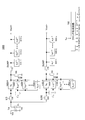
- FIG. 8 is a block diagram showing an example of a main configuration of the discrete time analog circuit 13 according to the present embodiment.
- a discrete-time analog circuit 100 corresponds to the discrete-time analog circuit 13 of FIG. 7, and constitutes a sampling mixer.
- a discrete-time analog circuit 100 includes a clock generation circuit 110, a TA (Transconductance Amplifier: voltage-current conversion circuit (transconductance value: gm)) 120, a sampling switch 130, a coefficient circuit 140, a rotate capacitor circuit 150, and a reset switch. 160 and a dump switch 170.
- TA Transconductance Amplifier: voltage-current conversion circuit (transconductance value: gm)
- the discrete-time analog circuit 100 shown in FIG. 8 shows a configuration having a coefficient circuit 140 in the previous stage of the rotate capacitor circuit 150, and is hereinafter referred to as a pre-stage discrete-time analog circuit.
- the coefficient circuit 140 is connected to the input line of the rotate capacitor circuit 150.
- the coefficient circuit 140 includes CH (history capacitors) 143-1, 143-2 (a1, a2), an amplifier 141 (b), connection changeover switches (hereinafter referred to as switches) 142-1 to 142-4 (c1-c4).
- CH history capacitors
- 143-2 a1, a2
- amplifier 141 b
- connection changeover switches hereinafter referred to as switches
- the coefficient circuit 140 realizes a coefficient having an arbitrary first-order value of the denominator of the transfer function of the discrete-time analog circuit 100 by sharing the charge with the rotate capacitor circuit 150 (internal charge holding circuit). To do.
- the coefficient circuit 140 receives control signals S 1 and S 2 from the clock generation circuit 110.
- the amplifier 141 (b) is connected to the input line of the rotate capacitor circuit 150 and functions as a potential holding means for amplifying the input potential or the input charge.
- the CHs 143-1 and 143-2 are connected in series with the amplifier 141 (b) and arranged in parallel with each other. CH143-1 and 143-2 function as charge holding means.
- the rotate capacitor circuit 150 includes switches 151-1 to 151-4 and CR (rotate capacitors) 152-1 and 152-2 (a3, a4).
- the clock generation circuit 110 provides a clock (control signal) to the sampling switch 130, the coefficient circuit 140, the switches 151-1 to 151-4, the reset switch 160, and the dump switch 170.
- FIG. 9 is a diagram illustrating a clock (control signal) provided from the clock generation circuit 110. Specifically, the clock generation circuit 110 generates LO, S1, S2, RES, and DUMP control signals from the reference frequency signal 24 generated by the reference frequency oscillating unit 14, and supplies the control signals to each switch.
- N represents a decimation ratio due to charge accumulation during charge sampling, and is 1/2 of the ratio between the LO period and the S-system clock (S1, S2) period.
- 2NTLO the ratio of the period of TSCLK, LO and the period of RES or DUMP.
- DUMP and RES are signals that are shifted by a half cycle.
- the clock generation circuit 110 generates LO, S1, S2, RES, and DUMP control signals from the reference frequency signal 24 generated by the reference frequency oscillating unit 14 and supplies the control signals to each switch.
- TA 120 converts analog RF signal 23 amplified by low noise amplifier 12 into an electric current (gm ⁇ Vin) as an input voltage signal.
- the sampling switch 130 is connected to the output stage of the TA 120 and is turned on only when the LO supplied from the clock generation circuit is high.
- the amplifier 141 monitors the output potential Vout, amplifies the output potential Vout A times, and charges the CH 143-1 (a1).
- the output potential Vout of CR 152-1 (a3) is output (Vout) as a baseband signal or an intermediate frequency (IF) signal 25. That is, the output potential Vout is subjected to filter processing by performing frequency conversion on the analog RF signal 23 in discrete time, and is output as a baseband signal (or IF signal) 25 from which only a desired signal component is extracted.
- the amplifier 141 (b) monitors the output potential Vout, amplifies the output potential Vout A times, and charges the CH 143-2 (a2).
- the output potential Vout of CR 152-1 (a3) is output as a baseband signal or IF signal 25. That is, the output potential Vout is subjected to filter processing by performing frequency conversion on the analog RF signal 23 in discrete time, and is output as a baseband signal (or IF signal) 25 from which only a desired signal component is extracted.
- the clock generation circuit 110 and each switch as circuit connection switching means sequentially change the pair of the first capacitor and the second capacitor.
- the first capacitor is a capacitor connected to the amplifier 141 (b) and charged.
- the second capacitor is a capacitor that is connected to the input line of the rotate capacitor circuit 150 without passing through the amplifier 141 (b) and shares the charge with the charge of the rotate capacitor circuit 150.
- Equation (2) q in (n) in the first term on the left side corresponds to the input charge, and the second term on the left side is the charge held in CH by multiplying the output potential one timing before by A. N indicates the timing time.
- Equation (3) is obtained by z-transforming Equation (2).
- the transfer function is as shown in the following equation (5).
- the discrete-time analog circuit according to the present embodiment can set an arbitrary coefficient value by applying the weighting amount A to the denominator z- N coefficient.
- FIG. 10 is a diagram showing another main configuration of the discrete-time analog circuit 13 according to the present embodiment.
- a discrete-time analog circuit 200 corresponds to the discrete-time analog circuit 13 of FIG. 7, and constitutes a sampling mixer.
- the discrete-time analog circuit 200 in FIG. 10 has a configuration in which a coefficient circuit 220 is provided instead of the coefficient circuit 140 and CH 210 (a5) is added to the discrete-time analog circuit 100 in FIG.
- the 10 has a configuration having a coefficient circuit 220 in the subsequent stage of the rotate capacitor circuit 150, and is hereinafter referred to as a post-stage discrete-time analog circuit.
- the coefficient circuit 140 is connected to the output line of the rotate capacitor circuit 150.
- the coefficient circuit 220 includes CB (buffer capacitors) 223-1, 223-2 (a1, a2), an amplifier 221 (b), and switches 222-1 to 222-4 (c1-c4).
- the CBs 223-1, 223-2 (a 1, a 2) in the coefficient circuit 220 share charges with CR 152-1 and 152-2 (a 3, a 4), thereby denominating the transfer function of the discrete-time analog circuit 200.
- the coefficient circuit 220 receives control signals S 1 and S 2 from the clock generation circuit 110.
- FIG. 11 is a diagram illustrating a clock (control signal) provided from the clock generation circuit 110.
- the amplifier 221 (b) is connected to the output line of the rotate capacitor circuit 150 and functions as a potential holding means for amplifying the output potential or the output charge.
- the CBs 223-1, 223-2 (a1, a2) are connected in series with the amplifier 221 (b) and arranged in parallel with each other.
- the CBs 223-1 and 223-2 (a1, a2) function as charge holding means.
- the clock generation circuit 110 generates LO, S1, S2, RES, and DUMP control signals from the reference frequency signal 24 generated by the reference frequency oscillating unit 14 and supplies the control signals to each switch.
- TA 120 converts analog RF signal 23 amplified by low noise amplifier 12 into an electric current (gm ⁇ Vin) as an input voltage signal.
- CR152-2 (a4) and CB223-2 (a2) are connected in the section where DUMP is high.
- the charge held in CR 152-2 (a4) and the charge held in CB 223-2 (a2) (charge multiplied by A) are shared.
- the shared charge is held in CR 152-2 (a4) and CB 223-2 (a2), and the output potential Vout is determined.
- the amplifier 221 (b) monitors the output potential Vout, amplifies the output potential Vout A times, and charges the CB 223-1 (a1).
- the output potential Vout is output as a BB signal or IF signal 25 obtained by frequency-converting the analog RF signal 23 and performing a filter process. Further, in a section where RES is high, DUMP is low, and the charge of CR 152-2 (a4) is grounded and reset.
- CR152-1 (a3) and CB223-1 (a1) are connected in the section where DUMP is high.
- the charge held in CR 152-1 (a3) and the charge held in CB 223-1 (a1) charges accumulated by multiplying by A) are shared.
- the shared charge is held in CR 152-1 (a3) and CB 223-1 (a1), and the output potential Vout is determined.
- the amplifier 221 (b) monitors the output potential Vout, amplifies the output potential VoutA times, and charges the CB 223-2 (a2).
- the output potential Vout is output as a BB signal or IF signal 25 obtained by subjecting the analog RF signal 23 to frequency conversion and filtering. Further, during the period when RES is high, the charge of CR 152-1 (a3) is reset to ground.
- the clock generation circuit 110 and each switch as circuit connection switching means sequentially change the pair of the first capacitor and the second capacitor.
- the first capacitor is a capacitor connected to the amplifier 221 (b) and charged.
- the second capacitor is a capacitor that is connected to the output line of the rotate capacitor circuit 150 without going through the amplifier 221 (b) and shares the charge with the charge of the rotate capacitor circuit 150.
- the first term on the left side is the charge held in CR
- the second term on the left side is the charge held in CB by multiplying the potential determined by charge sharing one timing before by A. .
- the discrete-time analog circuit according to the present embodiment can set an arbitrary coefficient value by applying the weighting amount A to the denominator z- N coefficient.
- the discrete-time analog circuit 200 described above is an example in which a buffer capacitor constituting a sampling mixer is used as a component of a coefficient circuit.
- the sampling filter described below is an example in which a buffer capacitor is used as a component of a coefficient circuit.
- FIG. 12 is a diagram showing still another main configuration of the discrete-time analog circuit 13 according to the present embodiment.
- the discrete-time analog circuit 300 constitutes a sampling filter.
- the discrete time analog circuit 300 of FIG. 12 adopts a configuration in which the TA 120, the sampling switch 130, the CH 210, the reset switch 160, and the dump switch 170 are deleted from the discrete time analog circuit 200 of FIG.
- the discrete-time analog circuit 300 is a latter-stage discrete-time analog circuit having a coefficient circuit 220 at the subsequent stage of the rotate capacitor circuit 150.
- the clock generation circuit 110 generates S1 and S2 control signals from the reference frequency signal 24 generated by the reference frequency oscillating unit 14, and supplies the control signals to each circuit.
- the charge accumulated in CR 152-2 (a4) and the charge accumulated in CB 223-2 (a2) are shared.
- the shared charge is held in CR 152-2 (a4) and CB 223-2 (a2), and the output potential Vout is determined.
- the amplifier 221 (b) monitors the output potential Vout, amplifies the output potential Vout A times, and charges the CB 223-1 (a1).
- the charge accumulated in CR 152-1 (a3) and the charge accumulated in CB 223-1 (a1) are shared.
- the shared charge is held in CR 152-1 (a3) and CB 223-1 (a1), and the output potential Vout is determined.
- the amplifier 221 (b) monitors the output potential Vout, amplifies the output potential Vout A times, and charges the CB 223-2 (a2).
- the transfer function is as follows when formula (9) is rearranged by z-transform.
- the discrete-time analog circuit according to the present embodiment can set an arbitrary coefficient value by applying the weighting amount A to the denominator z- N coefficient.
- the coefficient circuit 220 in FIG. 12, be connected to the V in can be configured as a front-type sampling filter having a transfer function similar to the equation (10).
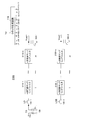
- FIG. 13 is a diagram for explaining the operation of the coefficient circuits 140 and 220.
- FIG. 13B shows a usage example of the former-stage type coefficient circuit 140
- FIG. 13C shows a usage example of the latter-stage type coefficient circuit 220
- FIG. 13A is a diagram illustrating a common operation of the front-stage type coefficient circuit 140 and the rear-stage type coefficient circuit 220.
- the input charge and the charge held in CH 143-2 perform charge sharing, and the shared charge is multiplied by A to charge CH 143-1.
- the operation is repeated alternately.
- the coefficient circuit according to the present embodiment can form an arbitrary coefficient value in the denominator of the transfer function as shown in Expression (5), Expression (8), and Expression (10).
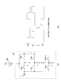
- FIG. 14 is a diagram showing a common configuration of the coefficient circuits 140 and 220.
- the coefficient circuit 400 includes capacitors 430-1 and 430-2 (a1, a2), an amplifier 410 (b), and switches 420-1 to 420-4 (c1-c4).
- the coefficient circuit 400 receives S1 and S2 from the clock generation circuit 110.
- the amplifier 410 (b) amplifies the potential of the node Cin A times.
- the switch 420-4 (c4) and the switch 420-1 (c1) are turned on.
- the capacitor 430-2 (a2) is connected to the external circuit at the node Cin via the switch 420-4 (c4).
- the electric charge corresponding to the potential amplified by A times by the amplifier 410 (b) is accumulated in the capacitor 430-1 (a1) via the switch 420-1 (c1).
- the switch 420-2 (c2) and the switch 420-3 (c3) are turned on.
- the capacitor 430-1 (a1) is connected to the external circuit at the node Cin via the switch 420-2 (c2).
- the electric charge corresponding to the potential amplified by A times by the amplifier 410 (b) is accumulated in the capacitor 430-2 (a2) via the switch 420-3 (c3).
- the node Cin is alternately connected to the CR 152-1 and 152-2 having an initial charge of 0 in the discrete-time analog circuit 100 shown in FIG.
- the discrete-time analog circuit 200 shown in FIG. 10 is an example in which the node Cin is alternately connected to the CR 152-1 and 152-2 of the initial charge CrVin (n ⁇ 1).
- 12 is an example in which the node Cin is connected to the CR 152-1 and 152-2 of the initial charge CrVin (n ⁇ 1).
- the initial charges of the CR 152-1 and 152-2 to which the node Cin is connected differ between the former type and the latter type.
- the capacitor 430-1 (a1) functions as charge holding means.
- the capacitors 430-1 and 430-1 (a1, a2) are CH143-1 and 143-2.
- the capacitors 430-1 and 430-1 (a1, a2) are CB 223-1, 223-2.
- the amplifier 410 (b) functions as a potential holding unit.
- Each switch and clock generation circuit 110 functions as a circuit connection switching unit, and switches connection between the rotate capacitor and the capacitors 430-1 and 430-1 (a1, a2) at timing 1 and timing 2.
- 8 and 10 can perform filter processing represented by a transfer function having a first-order term having an arbitrary coefficient in the denominator as well as frequency conversion by charge sampling. Both differ in whether or not a denominator coefficient circuit is connected or not at the time of charge sampling for frequency conversion, and are considered to affect noise and linearity.
- the coefficient circuit 220 shown in FIG. 12 is a circuit that can perform a filter process represented by a transfer function having a first-order term having an arbitrary coefficient in the denominator.
- the configuration of FIG. 12 can be used as a filter circuit because there is no voltage-current conversion circuit that performs charge sampling and a sampling switch.
- the design freedom of the discrete-time analog circuit is improved, and a broadband and steep filter characteristic is realized. Is possible.
- Patent Document 1 and Non-Patent Document 1 FIR filter characteristics are obtained by preparing a plurality of rotate capacitors, holding sample values with different timings, and simultaneously outputting them.
- the above configuration is omitted, but the same configuration can be used.
- Patent Document 1 and Non-Patent Document 1 the rotation capacitor is precharged by a feedback system.
- the above configuration is omitted, but the same configuration can be used.
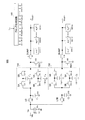
- FIG. 15 is a block diagram showing an example of a main configuration of the discrete time analog circuit 13 according to the present embodiment.
- a discrete time analog circuit 500 corresponds to the discrete time analog circuit 13 of FIG. 7, and constitutes a sampling mixer having a second-order coefficient in the denominator of the transfer function.
- the discrete time analog circuit 500 of FIG. 15 employs a configuration in which a coefficient circuit 510 and a buffer capacitor 520 are added to the discrete time analog circuit 100 of FIG.
- the discrete-time analog circuit 500 employs a configuration having the coefficient circuit 140 and the coefficient circuit 510 in the previous stage of the rotate capacitor circuit 150.
- the discrete-time analog circuit 500 realizes a second-order polynomial in the denominator of the transfer function by using two coefficient circuits 140 and 510.
- the coefficient circuit 510 includes an amplifier 511 (b2), switches 512-1 to 512-6, and CH (history capacitors) 513-1 to 513-3 (a3-a5).
- the clock generation circuit 110 generates the control signals LO, SA, SB, DUMP, RES, S1, S2, and S3 shown in FIG. 16 from the reference frequency signal 24 generated by the reference frequency oscillating unit 14, and supplies the control signals to each switch. To do.
- TA 120 converts analog RF signal 23 amplified by low noise amplifier 12 into an electric current (gm ⁇ Vin) as an input voltage signal.
- the coefficient circuit 140 operates in the same manner as in the first embodiment, the description thereof is omitted, and the following description will focus on the operation of the coefficient circuit 510.
- the input current (gm ⁇ Vin) is CH143-1 (a1) or CH143-2 (a2) and CR152-1 (a6) or CR152- 2 (a7) and CH513-2 (a4) are accumulated as charges (input charges).
- the shared charge is held in CH143-1 (a1) or CH143-2 (a2), CH513-2 (a4), and CR152-1 (a6) or CR152-2 (a7).
- the potential V1 is determined.
- the discrete-time analog circuit 500 performs frequency conversion simultaneously, and the RF signal is converted into an IF signal or a BB signal.
- the amplifier 141 (b1) amplifies the potential V1 by A1 and charges a capacitor that does not share charge with CH513-2 (a4) of CH143-1 (a1) or CH143-2 (a2).
- the amplifier 511 (b2) monitors the potential V1, amplifies the potential V1 to A2 times, and charges CH513-1 (a3).
- CB520 (a8) holds the charge held by the capacitor that does not share charge with CH513-2 (a4) of CR152-1 (a6) or CR152-2 (a7).
- Charges are shared. The shared charge is held in CH513-2 (a4) and the capacitor that does not share charge and CB520 (a8) of CR152-1 (a6) or CR152-2 (a7), and the output potential Vout is Determined.
- the output potential Vout is output as the baseband signal 25.
- DUMP is low, and the charge of the capacitor that does not share charge with CH513-2a4 in CR 152-1 (a6) or CR 152-2 (a7) is grounded and reset.
- the input current is CH143-1 (a1) or CH143-2 (a2), CR152-1 (a6) or CR152-2 (a7), Accumulated as charge (input charge) in CH513-3 (a5).
- the shared charge is held in CH143-1 (a1) or CH143-2 (a2), CH513-3 (a5), CR152-1 (a6) or CR152-2 (a7), and the potential is V1 is determined.
- the amplifier 141 (b1) monitors the potential V1, amplifies the potential V1 by A1, and does not share charge with CH513-3 (a5) of CH143-1 (a1) or CH143-2 (a2). Charge the capacitor. Then, the amplifier 511 (b2) monitors the potential V1, amplifies the potential V1 to A2 times, and charges CH513-2 (a4).
- CB520 (a8) holds the charge held by the capacitor that does not share charge with CH513-3 (a5) of CR152-1 (a6) or CR152-2 (a7). Charges are shared. The shared charge is held in CB520 (a8) and the capacitor that does not share charge with CH513-3 (a5) of CR152-1 (a6) or CR152-2 (a7), and the output potential Vout is determined. .
- DUMP is low, and the charge of the capacitor of CR 152-1 (a6) or CR 152-2 (a7) that does not share charge with CH 513-3 (a5) is grounded and reset.
- the input current is CH143-1 (a1) or CH143-2 (a2), CR152-1 (a6) or CR152-2 (a7), Accumulated as charge (input charge) in CH513-1 (a3).
- the charge held in CH143-1 (a1) or CH143-2 (a2), the charge held in CH513-1 (a3), and the input charge share charges.
- the shared charge is held in CH143-1 (a1) or CH143-2 (a2), CH513-1 (a3), and CR152-1 (a6) or CR152-2 (a7), and the potential V1 is Determined.
- the amplifier 141 (b1) monitors the potential V1, amplifies the potential V1 to A1 times, and does not share charge with CH513-1 (a3) of CH143-1 (a1) or CH143-2 (a2). Charge the capacitor. Then, the amplifier 511 (b2) monitors the potential V1, amplifies the potential V1 to A2 times, and charges CH513-3 (a5).
- CB520 (a8) holds the charge held by the capacitor that does not share charge with CH513-1 (a3) of CR152-1 (a6) or CR152-2 (a7). Charges are shared. Then, the shared charge is held in CH 513-1 (a3) and the capacitor not sharing charge with CB 520 (a8) of CR 152-1 (a6) or CR 152-2 (a7), and the output potential Vout is Determined.
- the charge of the capacitor that does not share charge with CH 513-1 (a3) is grounded and reset.
- the discrete-time analog circuit provides a transfer function by providing a timing of waiting for one timing before the charge weighted and held by the amplifier 511 (b2) performs charge sharing.
- a quadratic term is realized in the denominator.
- the first term on the left side corresponds to the input charge
- the second term is the charge held in CH1 by multiplying the potential determined by charge sharing one timing before by A1.
- the third term on the left side is the charge held in CH2 by multiplying the potential determined by charge sharing two timings before by A2.
- the transfer function is expressed by the following equation (13) when the equations (11) and (12) are rearranged by z-transform.
- the discrete-time analog circuit according to the present embodiment can realize a second-order polynomial having an arbitrary coefficient in the denominator of the transfer function, as shown in Expression (13) and Expression (14).
- the discrete-time analog circuit 500 described above is an example of a pre-stage type using a history capacitor as a component of a coefficient circuit.
- the latter-stage discrete-time analog circuit 200 using the buffer capacitor as a component of the coefficient circuit can realize a second-order term in the denominator of the transfer function.
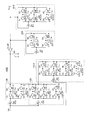
- FIG. 17 is a block diagram showing an example of another main configuration of the discrete-time analog circuit 13 according to the present embodiment.
- a discrete time analog circuit 600 corresponds to the discrete time analog circuit 13 of FIG. 7, and constitutes a sampling mixer having a second-order coefficient in the denominator of the transfer function.
- the discrete time analog circuit 600 of FIG. 17 employs a configuration in which a coefficient circuit 610 is added to the discrete time analog circuit 200 of FIG.
- the discrete-time analog circuit 600 has a configuration having a coefficient circuit 220 and a coefficient circuit 610 in the subsequent stage of the rotate capacitor circuit 150.
- the discrete-time analog circuit 600 realizes a second-order polynomial in the denominator of the transfer function.
- the coefficient circuit 610 includes an amplifier 611 (b2), switches 612-1 to 612-6, and CB (buffer capacitors) 613-1 to 613-3 (a3-a5).
- the clock generation circuit 110 generates LO, SA, SB, S1, S2, S3, RES, and DUMP control signals from the reference frequency signal 24 generated by the reference frequency oscillating unit 14, and supplies the control signals to each circuit.
- TA 120 converts analog RF signal 23 amplified by low noise amplifier 12 into an electric current (gm ⁇ Vin) as an input voltage signal.
- the coefficient circuit 220 operates in the same manner as in the first embodiment, the description thereof will be omitted, and the following description will focus on the operation of the coefficient circuit 610.
- the discrete-time analog circuit 600 performs frequency conversion simultaneously, and the RF signal is converted into an IF signal or a BB signal.
- CB buffer capacitor
- Capacitors that do not share charge are the charge held by itself, the charge held by CB223-1 (a1) or CB223-2 (a2) (multiplied by A1), and the charge held by CB613-2a4 (A2 times).
- the shared charge includes CR152-1 (a6) or CR152-2 (a7), a capacitor that does not share charge with CH210 (a8), CB613-2 (a4), CB223-1 (a1), or CB223-2. (a2). Thereby, the output potential Vout is determined.
- the amplifier 221 (b1) monitors the output potential Vout, amplifies the output potential Vout by A1, and selects CB613-2 (a4) of CB223-1 (a1) or CB223-2 (a2). Charge a capacitor that does not share charge.
- the amplifier 611 (b2) monitors the output potential Vout, charges the output potential Vout by A2, and charges the CB 613-1 (a3).
- the output potential Vout is output as the baseband signal 25.
- a capacitor that does not share charge with CH210 (a8) in CR152-1 (a6) or CR152-2 (a7) is shared with CB (buffer capacitor) shown below.
- the capacitor that does not share the charge is held by the charge held by itself, the charge held by CB223-1 (a1) or CB223-2 (a2) (multiplied by A1), and CB613-3 (a5).
- the shared charge includes CR152-1 (a6) or CR152-2 (a7), a capacitor that does not share charge with CH210 (a8), CB613-3 (a5), CB223-1 (a1), or CB223- 2 (a2).
- the output potential Vout is determined.
- the amplifier 221 (b1) monitors the output potential Vout, amplifies the output potential Vout by A1, and does not share the charge with CB613-3 (a5) at CB223-1 (a1) or CB223-2 (a2). Charge the capacitor.
- the amplifier 611 (b2) monitors the output potential Vout, multiplies the output potential Vout by A2, and charges the CB 613-2 (a4).
- a capacitor that does not share charge with CH210 (a8) in CR152-1 (a6) or CR152-2 (a7) is shared with CB (buffer capacitor) shown below.
- the Capacitors that do not share charge are held by CB 613-1 (a3), CB 223-1 (a1), CB 233-1 (a2), and CB 613-1 (a3). Share the same charge (A2 times).
- the shared charge includes CR152-1 (a6) or CR152-2 (a7), a capacitor that does not share charge with CH210 (a8), CB613-1 (a3), CB223-1 (a1), or CB223. -2 (a2). Thereby, the output potential Vout is determined.
- the amplifier 221 (b1) monitors the output potential Vout, amplifies the output potential Vout by A1 times, and selects CB613-1 (a3) of CB223-1 (a1) or CB223-2 (a2). Charge a capacitor that does not share charge.
- the amplifier 611 (b2) monitors the output potential Vout, charges the output potential Vout by A2, and charges the CB 613-3 (a5).
- the discrete-time analog circuit provides a second-order denominator of the transfer function by providing a timing for waiting for one timing before the charge weighted and held by the amplifier 611 (b2) performs charge sharing. Is realized.
- the transfer function is as follows when formula (16) is rearranged by z-transform.
- the discrete-time analog circuit according to the present embodiment can realize a second-order polynomial having an arbitrary coefficient in the denominator of the transfer function T IIR as shown in equations (17) and (18).
- the transconductance gm of the TA 120 is expressed as follows: The value of each capacitor is set as follows.
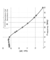
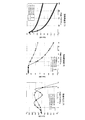
- FIG. 18 shows a calculation result (denominator Cal) of a molecular constant (a DC gain is set to be 26 dB differentially) in the equation (19) having a coefficient of Chebyshev characteristics.
- FIG. 18 shows a simulation result (denominator Sim) by SPICE (Simulation Program with Integrated Circuit Emphasis). The horizontal axis in FIG. 18 indicates the frequency after frequency conversion. DC (0 Hz) in FIG. 18 corresponds to the LO frequency. Calculations and simulations were performed with an LO frequency of 1.5 GHz. In the simulation, in the configuration of the discrete-time analog circuit 600 in FIG. 17, ideal TA120, each switch, and each capacitor were used. Further, the values of the history capacitor and the rotate capacitor are made equal so that the ripple due to the Chebyshev characteristic appears clearly.
- the discrete-time analog circuit according to the present embodiment can realize a polynomial having an arbitrary second-order coefficient value in the denominator of the transfer function of the discrete-time analog circuit.
- FIG. 15 and FIG. 17 can perform filter processing represented by a transfer function having a second-order polynomial having an arbitrary coefficient in the denominator, along with frequency conversion by charge sampling. Both differ in whether or not a denominator coefficient circuit is connected or not at the time of charge sampling for frequency conversion, and are considered to affect noise and linearity.
- the discrete-time analog circuit can perform filter processing represented by a transfer function having a second-order polynomial having an arbitrary coefficient in the denominator together with frequency conversion.
- the second embodiment has described the discrete-time analog circuit that can realize a polynomial having an arbitrary second-order coefficient value in the denominator of the transfer function.
- a discrete-time analog circuit that extends the order to the nth order and realizes a polynomial having an arbitrary coefficient value of the nth order in the denominator of the transfer function will be described.
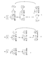
- FIG. 19 is a diagram for explaining a procedure for increasing the order of the coefficient circuit.
- FIG. 19A shows a primary configuration. In the first-order procedure, the timing of holding and multiplying by A and the timing of charge sharing are repeated alternately. In the difference equation expressing charge sharing, a term of v (n ⁇ 1) appears, so that a first order term can be realized.
- FIG. 19B shows a secondary configuration.
- a “waiting” timing is provided between the timing of holding and multiplying by A and the timing of charge sharing.
- FIG. 19C shows a k-th order configuration.
- k ⁇ 1 “waiting” timings are provided between the timing of preparing k + 1 capacitors in the coefficient circuit, holding and multiplying them by A, and the timing of charge sharing.
- v (n ⁇ k) appears, so that a k-th order term can be realized.
- FIG. 20 (a) is a diagram showing a circuit configuration of the coefficient circuit 700 expanded to the kth order.
- the coefficient circuit 700 includes k + 1 capacitors and 2 ⁇ (k + 1) switches.
- FIG. 20B is a diagram illustrating a timing diagram of Sk0 to Skk input to each switch of the coefficient circuit 700.
- the coefficient circuit 700 inputs the clocks indicated by Sk0 to Skk, thereby setting the first capacitor at the i-th timing as the second capacitor at the i + n ⁇ 1 timing. In addition, the coefficient circuit 700 sets the second capacitor at the i-th timing as the first capacitor at the i + 1-th timing. As a result, the coefficient circuit 700 can realize a k-th order term. Furthermore, the coefficient circuit 700 can set the coefficient value to an arbitrary value by multiplying the potential by A when holding the potential.
- the value of the capacitor is set to one Ck.
- the degree of freedom in filter design can be improved by changing each Ck value to an appropriate value.
- FIG. 21 is a diagram showing a configuration example in which the discrete-time analog circuit 500 of FIG.
- the discrete-time analog circuit 800 in FIG. 21 has a system connected to the sampling switch 820 in addition to the system connected to the sampling switch 130, and has a differential configuration.
- LO is input to the sampling switch 130 and LOB is input to the sampling switch 830.
- LOB is a signal that is 180 degrees out of phase with LO
- the system connected to the sampling switch 820 to which LOB is input operates as a differential anti-phase system.
- FIG. 22 is a diagram illustrating a clock (control signal) input to the discrete-time analog circuit 800 of FIG.
- the first term on the left side is the input charge.
- the transfer function is as follows when the equation (21) is rearranged by z-transform.
- the discrete-time analog circuit according to the present embodiment can realize a transfer function having an arbitrary order coefficient in the denominator, as shown in Expression (22) and Expression (23).
- Expression (22) and Expression (23) As a result, the number and value of the poles of the transfer function can be arbitrarily set, and the degree of freedom in filter design can be improved.
- FIG. 23 is a diagram illustrating a configuration example in which the discrete-time analog circuit 200 of FIG.
- 23 has a system connected to the sampling switch 820 in addition to the system connected to the sampling switch 130.
- the discrete-time analog circuit 900 shown in FIG. LO is input to the sampling switch 130 and LOB is input to the sampling switch 820.
- LOB is a signal that is 180 degrees out of phase with LO
- the system connected to the sampling switch 820 to which LOB is input operates as a differential anti-phase system.
- the discrete time analog circuit 900 receives a clock (control signal) shown in FIG.
- the transfer function is expressed by the following equation (26) when the equation (25) is rearranged by z-transform.
- the discrete-time analog circuit according to the present embodiment can realize a transfer function having an arbitrary order coefficient in the denominator, as shown in equations (26) and (27).
- equations (26) and (27) the number and value of the poles of the transfer function can be arbitrarily set, and the degree of freedom in filter design can be improved.
- n 1 or more
- FIG. 21 and FIG. 23 can perform filter processing represented by a transfer function having an n-th order polynomial having an arbitrary coefficient in the denominator as well as frequency conversion by charge sampling. Both differ in whether or not a denominator coefficient circuit is connected or not at the time of charge sampling for frequency conversion, and are considered to affect noise and linearity.
- the discrete-time analog circuit according to the present embodiment is capable of arbitrarily setting the transfer function pole represented by a transfer function having an n-th order polynomial having an arbitrary coefficient in the denominator. It becomes possible to do.
- FIG. 24 is a diagram showing the configuration of the coefficient circuit 1000 used in the molecular-type discrete-time analog circuit and the clock input to the coefficient circuit 1000.
- the coefficient circuit 1000 includes CR (rotate capacitors) 1030-1, 1030-2 (a1, a2), an amplifier 1010 (b), and switches 1020-1 to 1020-4 (c1-c4).
- the coefficient circuit 1000 receives S1 and S2 from a clock generation circuit (not shown).
- FIG. 24A shows a charge sharing type coefficient circuit
- FIG. 24B shows a potential holding type coefficient circuit.
- the potential holding type coefficient circuit of FIG. 24B will be described.
- the clock generation circuit 110 supplies control signals S1 and S2 to each switch.
- the amplifier 1010 (b) monitors the potential of the node Cin, amplifies the potential of the node Cin B times, and transmits the CR 1030-1 via the switch 1020-1 (c1). Accumulate in (a1).
- the CR 1030-2 (a2) is connected to an external circuit at the node Cout via the switch 1020-4 (c4).
- the amplifier 1010 (b) monitors the potential of the node Cin, amplifies the potential of the node Cin by B times, and passes through the switch 1020-3 (c3) to CR1030-2. Accumulate in (a2). At the same time, the CR 1030-1 (a1) is connected to an external circuit at the node Cout via the switch 1020-2 (c2).
- FIG. 25 is a diagram showing a main configuration of the discrete-time analog circuit 13 according to the present embodiment.
- a discrete-time analog circuit 1100 corresponds to the discrete-time analog circuit 13 of FIG. 7 and constitutes a sampling mixer.
- the same reference numerals as those in FIG. 8 are given to the same components as those in the discrete-time analog circuit 100 in FIG.
- the discrete-time analog circuit 1100 of FIG. 25 has a coefficient circuit 1120 instead of the coefficient circuit 140, and adds CH (history capacitor) 1110 and CB (buffer capacitor) 1130 to the discrete-time analog circuit 100 of FIG. Adopted the configuration.
- the coefficient circuit 1120 includes an amplifier 1121 (b), switches 1122-1 to 1122-6, and CR (rotate capacitors) 1123-1 to 1123-3 (a4, a5, a6).
- the discrete-time analog circuit 1100 in FIG. 25 has a coefficient circuit 1120 in parallel with the rotate capacitor circuit 150 to increase the numerator of the transfer function.
- the clock generation circuit 110 generates LO, SA, SB, S1, S2, S3, RES, and DUMP control signals shown in FIG. 26 from the reference frequency signal 24 generated by the reference frequency oscillating unit 14, and supplies the control signals to each switch. To do.
- TA 120 converts analog RF signal 23 amplified by low noise amplifier 12 into an electric current (gm ⁇ Vin) as an input voltage signal.
- the amplifier 1121 (b) monitors the potential V1, amplifies the potential V1 B times, and charges the CR 1123-1 (a4).
- the discrete-time analog circuit 1100 performs frequency conversion at the same time, and the RF signal is converted into an IF signal or a BB signal.
- CR152-1 (a2) or CR152-2 (a3), CR1123-2 (a5), and CB1130 share the charge held by each.
- the output potential Vout is determined.
- the output potential Vout is output as an IF signal or a BB signal 25.
- the amplifier 1121 (b) monitors the potential V1, amplifies the potential V1 to B times, and charges the CR 1123-1 (a5).
- CR152-1 (a2) or CR152-3 (a3), CR1123-3 (a6), and CB1130 buffer capacitor share the charge held by each. Thereby, the output potential Vout is determined.
- the output potential Vout is output as an IF signal or a BB signal 25.
- the amplifier 1121 (b) monitors the potential V1, amplifies the potential V1 B times, and charges the CR 1123-3 (a6).
- CR152-1 (a2) or CR152-2 (a3), CR1123-1 (a4), and CB1130 share the charge held by each.
- the output potential Vout is determined.
- the output potential Vout is output as an IF signal or a BB signal 25.
- the first term on the left side is the input charge.
- the second term on the left side is a charge determined by charge sharing one timing before held in CH.
- the first term on the left side is the charge held in CR0.
- the second term on the left side is obtained by multiplying the potential determined by the charge sharing on the input side one timing before the charge sharing on the input side by B1 by the amount of charge held in CR0 by B1. Charge held in CR1.
- the third term on the left is a charge determined by charge sharing on the output side held one timing before held in CB.
- the transfer function is as follows when formula (29) is rearranged by z-transform.
- the discrete-time analog circuit according to the present embodiment can realize a first-order polynomial having a constant term and an arbitrary coefficient in the numerator of the transfer function T IIR as shown in Expression (30) and Expression (31).
- the coefficient circuit 1000 is configured to use both the charge sharing type and the potential holding type.
- the coefficient circuit 1000 can be configured only by the charge sharing type or only by the potential holding type.
- the amplifier 1121 When only the charge sharing type is used, the amplifier 1121 becomes a simple wiring. The difference in operation is that CR1 is also added to charge sharing between the input charge and CH and CR0, and CR1 is not multiplied by B1.
- the transfer function is as follows.
- the discrete-time analog circuit according to the present embodiment can realize a first-order polynomial having a constant term and an arbitrary coefficient in the numerator of the transfer function T IIR as shown in the equations (34) and (35).
- FIG. 27 is a diagram showing a main configuration of the discrete time analog circuit 13 according to the present embodiment.
- a discrete-time analog circuit 1200 corresponds to the discrete-time analog circuit 13 in FIG. 7 and constitutes a sampling mixer.
- the same reference numerals as those in FIG. 25 are assigned to the same components as those of the discrete-time analog circuit 1100 of FIG.
- the discrete-time analog circuit 1200 of FIG. 27 employs a configuration in which an amplifier 1210 is added between the CH 1110 and the rotate capacitor circuit 150 with respect to the discrete-time analog circuit 1100 of FIG.
- the clock generation circuit 110 generates LO, SA, SB, S1, S2, S3, RES, and DUMP control signals shown in FIG. 28 from the reference frequency signal 24 generated by the reference frequency oscillating unit 14, and supplies the control signals to each switch. To do.
- TA 120 converts analog RF signal 23 amplified by low noise amplifier 12 into an electric current (gm ⁇ Vin) as an input voltage signal.
- the amplifier 1210 (b1) monitors the potential V1, amplifies the potential V1 to B0 times, and charges the CR 152-1 (a2) or CR 152-2 (a3).
- the amplifier 1121 (b2) monitors the potential V1, amplifies the potential V1 to B1 times, and charges the CR 1123-1 (a4).
- the discrete time analog circuit performs frequency conversion at the same time, and converts the RF signal into an IF signal or a BB signal.
- CR152-1 (a2) or CR152-2 (a3), CR1123-2 (a5), and CB1130 share the charge held by each.
- the output potential Vout is determined.
- the output potential Vout is output as an IF signal or a BB signal 25.
- the amplifier 1210 (b1) monitors the potential V1, amplifies the potential V1 to B0 times, and charges the CR 152-1 (a2) or CR 152-2 (a3).
- the amplifier 1121 (b2) monitors the potential V1, amplifies the potential V1 to B1 times, and charges the CR 1123-2 (a5).
- the output potential Vout is determined.
- the output potential Vout is output as an IF signal or a BB signal 25.
- the amplifier 1210 (b1) monitors the potential V1, amplifies the potential V1 to B0 times, and charges the CR 151-1 (a2) or CR 151-2 (a3).
- the amplifier 1121 (b2) monitors the potential V1, amplifies the potential V1 to B1 times, and charges the CR 1123-3 (a6).
- CR152-1 (a2) or CR152-2 (a3), CR1123-1 (a4), and CB1130 share the charge held by each.
- the output potential Vout is determined.
- the output potential Vout is output as an IF signal or a BB signal 25.
- the transfer function is as follows when formula (37) is rearranged by z-transform.
- the discrete-time analog circuit according to the present embodiment can realize a first-order polynomial having a constant term and an arbitrary coefficient in the numerator of the transfer function T IIR as shown in equations (38) and (39).
- the DC gain is infinite, but in an actual circuit, the DC gain becomes a finite value due to the influence of the output resistance of the TA 120 and the parasitic capacitance.
- n-th order coefficient value is realized in the numerator of the transfer function in the same manner as when a polynomial having an n-th order coefficient value is realized in the denominator of the transfer function. it can.
- the order of the numerator terms of the transfer function is applied to the discrete-time analog circuit 1100 of FIG. 25 and the discrete-time analog circuit 1200 of FIG. Can be made higher.
- FIG. 29 is a diagram illustrating a configuration of a coefficient circuit (bkz ⁇ k ) 1300 that realizes a k-th order term, and a clock that is input from the clock generation circuit 110 to the coefficient circuit 1300.
- the discrete time analog circuit 1100 of FIG. 25 is obtained.
- the discrete-time analog circuit 1200 in FIG. 27 is obtained. That is, the difference between the discrete-time analog circuit 1100 and the discrete-time analog circuit 1200 depends on whether the constant term is realized by charge sharing or potential holding / weighting.
- the capacitor value is set to one CRk.
- the degree of freedom in filter design is improved by setting each CRk value to an appropriate value.
- FIG. 30 is a diagram showing a main configuration of a discrete-time analog circuit capable of realizing a polynomial having an arbitrary n-th order coefficient value of the numerator of the transfer function.
- the discrete-time analog circuit 1400 in FIG. 30 has molecular type coefficient circuits 1420-0 to 1420-n and 1430-0 to 1430-n, each of which has a configuration of charge sharing type or potential holding type. You may choose.
- the configuration of the coefficient circuits 1420-0 to 1420-n and 1430-0 to 1430-n is configured only by the charge sharing type, by combining the charge sharing type and the potential holding type, and This is a case where only a potential holding type is used.
- the differential equation representing the n-th order molecular charge sharing type operation of each of the charge sharing type, potential holding type, and the combination thereof, and the transfer function derived by z conversion are as follows.
- the transfer function is as follows when formula (41) is arranged by z conversion and arranged by z conversion.
- the transfer function is as follows when the equations (44) and (45) are rearranged by z-transform.
- the transfer function is as follows when the equations (48) and (49) are rearranged by z-transform.
- the discrete time analog circuit according to the present embodiment can realize a transfer function having an arbitrary order coefficient in the numerator of the transfer function, as shown in Expression (50) and Expression (51).
- 25 and 27 can perform a filter process represented by a transfer function having a second-order polynomial having an arbitrary coefficient in the numerator together with frequency conversion by charge sampling. Both differ in whether or not a numerator coefficient circuit is connected via an amplifier during charge sampling for frequency conversion, and makes a difference in the structure of the transfer function. Further, the difference is considered to affect noise and linearity.
- the charge holding circuit in the numerator coefficient circuit is used for charge sharing.
- the charge holding circuit in the numerator coefficient circuit charges the charge holding circuit in the molecular coefficient circuit with a charge corresponding to the amplified (held) potential.
- the discrete-time analog circuit can perform filter processing represented by a transfer function having an n-th order polynomial having an arbitrary coefficient in the denominator together with frequency conversion.
- FIG. 31 is a block diagram showing an example of a main configuration of the discrete time analog circuit according to the present embodiment.
- a discrete time analog circuit 1500 corresponds to the discrete time analog circuit 13 of FIG. 7, and constitutes a sampling mixer having a second-order polynomial in the numerator denominator of the transfer function.
- the same components as those in FIGS. 8, 17, and 27 are denoted by the same reference numerals and description thereof is omitted.
- a discrete-time analog circuit 1500 in FIG. 31 has a configuration in which a numerator coefficient circuit 1510 and denominator coefficient circuits 220 and 610 are added to the discrete-time analog circuit 1100 in FIG.
- the discrete-time analog circuit 1500 includes molecular coefficient circuits 150, 1120, and 1510 that are constituted by rotating capacitors, and coefficient circuits 220 and 610 that are constituted by buffer capacitors. As a result, the discrete-time analog circuit 1500 realizes quadratic polynomials for the numerator and denominator, respectively.
- a clock (control signal) shown in FIG. 33 is input from the clock generation circuit 110 to each switch of the discrete-time analog circuit 1500.
- V1 is determined by charge sharing between CH210 (a1) and CR0 together with the charge (CHv (n-N)) one timing before the input charge held in CH210 (a1).
- CR0 is CR152-1 (a2) or CR152-1 (a3).
- This V1 is held in CR1 at a potential B1 times by the amplifier 1121 (b1).
- CR1 is CR1123-1 (a5), CR1123-2 (a5), or CR1123-3 (a6).
- the potential is multiplied by B2 by the amplifier 1511 (b2), and is held in CR2 with the potential multiplied by B2.
- the output potential Vout is determined by charge sharing between the charge held in CB1 (A1CB1vout (nN)) and the charge held in CB2 (A2CB1vout (n-2N)).
- CB1 is CB223-1 (a11) or CB223-2 (a12).
- CB2 is CB613-1 (a13), CB613-2 (a14), or CB613-3 (a15).
- the Vout is held at CB1 at a potential A1 times by the amplifier 221 (b3) and held at CB2 at a potential A2 times by the amplifier 611 (b4).
- the transfer function is as follows when formula (53) is transformed by z conversion.
- the discrete-time analog circuit according to the present embodiment can realize a quadratic polynomial having arbitrary coefficients in the numerator and denominator of the transfer function TIIR . That is, the discrete-time analog circuit can realize a transfer function obtained by converting a secondary filter function in the s region into the z region by bilinear transformation using a sampling mixer.
- the difference in transfer function will be described in the explanation of the n-th order transfer function.
- FIG. 32 is a block diagram showing an example of another main configuration of the discrete-time analog circuit according to the present embodiment.
- a discrete-time analog circuit 1600 constitutes a sampling filter having a second-order coefficient in the denominator of the transfer function.
- the same reference numerals as those in FIG. 31 are attached to the same components as those in the discrete-time analog circuit 1500 in FIG.
- the discrete time analog circuit 1600 of FIG. 32 adopts a configuration in which TA 120 and CH 1110 are deleted from the discrete time analog circuit 1500 of FIG.
- the discrete-time analog circuit 1600 of FIG. 32 has a configuration in which an amplifier 1610 is added in front of the switches 152-1 and 152-2 (corresponding to changing the molecular charge sharing type coefficient circuit 150 to a molecular potential holding type). Take.
- the discrete-time analog circuit 1600 includes the molecular coefficient circuits 1120 and 1510 configured by rotating capacitors and the coefficient circuits 220 and 610 configured by buffer capacitors. As a result, the discrete-time analog circuit 1600 realizes quadratic polynomials for the denominator and the numerator, respectively.
- clock (control signal) shown in FIG. 33 is input from the clock generation circuit 110 to each switch of the discrete-time analog circuit 1600.
- the input potential Vin is held at CR0 at a potential B0 times by the amplifier 1610 (b0).
- CR0 is CR152-1 (a2) or CR152-1 (a3).
- the input potential Vin is held at CR1 at a potential B1 times by the amplifier 1121 (b1).
- CR1 is CR1123-1 (a5), CR1123-2 (a5), or CR1123-3 (a6).
- the potential is multiplied by B2 by the amplifier 1511 (b2), and the potential after B2 is held in CR2.
- CR2 is CR1513-1 (a7), CR1513-2 (a8), CR1513-3 (a9), or CR1513-4 (a10).
- the output potential Vout is determined by charge sharing between the charge held in CB1 (A1CB1vout (nN)) and the charge held in CB2 (A2CB1Vout (n ⁇ 2N)).
- CB1 is CB223-1 (a11) or CB223-2 (a12).
- CB2 is CB613-1 (a13), CB613-2 (a14), or CB613-3 (a15).
- This Vout is held at CB1 at a potential A1 times by the amplifier 221 (b3) and held at CB2 at a potential A2 times by the amplifier 611 (b4).
- the transfer function is as follows when formula (56) is rearranged by z-transform.
- the discrete-time analog circuit according to the present embodiment can realize a quadratic polynomial having arbitrary coefficients in the numerator and denominator of the transfer function T IIR as shown in Expression (57). That is, the discrete time analog circuit according to the present embodiment can realize the transfer function obtained by converting the filter function in the s region into the z region by bilinear transformation with the sampling filter.
- the difference in transfer function will be described in the explanation of the n-th order transfer function.
- an arbitrary coefficient value can be realized in the numerator denominator. Therefore, in the present embodiment, by comparing the numerator and denominator coefficients of Expression (58) with Expression (57), for example, the transconductance gm of TA120 and the value of each capacitor are set as follows. To do.
- 34 (a) and 34 (b) show a comparison between the calculation result of the second-order Chebyshev characteristic and the result of the SPICE simulation.
- the horizontal axis in FIG. 34 shows the frequency after frequency conversion.
- the solid line is the calculation result of the numerator denominator
- the dotted line is the calculation result of the denominator shown for reference.
- DC (0 Hz) in FIG. 34 corresponds to the LO frequency.
- the LO frequency was 1.5 GHz.
- an ideal TA 120, each switch, and each capacitor were used in the configuration of the discrete-time analog circuit 1600 of FIG.
- the values of the history capacitor CH and the rotate capacitor CR are made equal so that ripples due to the Chebyshev characteristic appear clearly.
- the calculation results and the simulation results agree well in a narrow band, and the discrete-time analog circuit 1600 performs the intended operation by adopting the configuration of FIG. I can confirm that.
- the denominator type deviates from the Chebyshev transfer function obtained by bilinear transformation around the sampling frequency / 2.
- the calculation result and the simulation result can be matched even in the broadband characteristics by increasing the numerator of the transfer function.
- the discrete-time analog circuit according to the present embodiment can realize a polynomial having an arbitrary order coefficient in the numerator and denominator of the transfer function, and can obtain a wide band and steep characteristics.
- polynomial coefficients having an arbitrary degree coefficient are realized not only in the denominator but also in the numerator, it is possible to arbitrarily set the number and values of poles of the transfer function, and the freedom of filter design The degree can be improved.
- the method of constructing the second-order polynomial of the molecule may be either a charge sharing type, a potential holding type, or a hybrid of both.
- the method of constructing the second-order polynomial of the denominator may be the former stage or the latter stage. The difference in transfer function will be described when the n-th order transfer function is described.
- the configuration of FIG. 31 can perform filter processing represented by a transfer function having a second-order polynomial having arbitrary coefficients in both the numerator denominator and frequency conversion by charge sampling.
- the discrete-time analog circuit can perform filter processing represented by a transfer function having a second-order term having arbitrary coefficients in both numerator denominators.
- FIG. 35 is a block diagram illustrating an example of a main configuration of the discrete-time analog circuit according to the present embodiment.
- a discrete-time analog circuit 1700 corresponds to the discrete-time analog circuit 13 of FIG. 7, and constitutes a sampling mixer having an nth-order coefficient in the denominator of the transfer function.
- the same components as those in FIGS. 21 and 30 are denoted by the same reference numerals as those in FIGS.
- the discrete-time analog circuit 1700 realizes n-order polynomials in the denominator and the numerator, respectively.
- the charge sharing operation of the discrete-time analog circuit 1700 is a combination of the nth-order numerator type and the nth-order preceding denominator type.
- the transfer function is as follows when formula (60) is rearranged by z-transform.
- the discrete-time analog circuit according to the present embodiment can realize a polynomial having an arbitrary order coefficient in the numerator denominator of the transfer function, as shown in Expression (61) and Expression (62), and can freely design a filter. The degree can be improved.
- FIG. 36 is a block diagram showing an example of another main configuration of the discrete-time analog circuit according to the present embodiment.
- the discrete-time analog circuit 1800 corresponds to the discrete-time analog circuit 13 in FIG. 7, and constitutes a sampling mixer having an n-th order coefficient in the denominator of the transfer function. Note that in the discrete-time analog circuit 1800 in FIG. 36, the same reference numerals as those in FIG.
- the charge sharing operation of the discrete-time analog circuit 1800 is a combination of the nth-order numerator type and the nth-order latter-stage denominator type.
- the transfer function is as follows when the equation (64) is rearranged by z-transform.
- the discrete-time analog circuit according to the present embodiment can realize a polynomial having an arbitrary order coefficient in the numerator denominator of the transfer function, as shown in Expression (65) and Expression (66). That is, in this embodiment, zero and pole can be set freely, so that the degree of freedom in designing the filter can be improved.
- the discrete-time analog circuit according to the present embodiment can provide a transfer function such as a numerator m-th denominator n-order by preparing m numerator-type coefficient circuits and n denominator-type coefficient circuits.
- n and m are integers of 0 or more.
- N 0 in the denominator coefficient circuit corresponds to a single capacitor (CH or CB) having no potential holding circuit.
- 35 and 36 can perform filter processing represented by a transfer function having an n-th order polynomial having arbitrary coefficients in both the numerator and the denominator, along with frequency conversion by charge sampling. Both differ in whether or not a denominator coefficient circuit is connected or not at the time of charge sampling for frequency conversion, and are considered to affect noise and linearity.
- the discrete-time analog circuit arbitrarily sets zeros and poles of a transfer function expressed by a transfer function having an n-th order polynomial having arbitrary coefficients in both the numerator and the denominator. It is possible to perform filter processing that can be set to
- n-order pre-stage sampling filter shown in FIG. 37 As basic components, there are an n-order pre-stage sampling filter shown in FIG. 37 and an n-order post-stage sampling filter shown in FIG.
- FIG. 37 is a block diagram showing an example of another main configuration of the discrete-time analog circuit according to the present embodiment.
- the discrete-time analog circuit 1900 constitutes a sampling filter having an nth-order coefficient in the denominator of the transfer function.
- the same reference numerals as those in FIG. 35 are given to the same components as those in the discrete-time analog circuit 1700 in FIG.
- the discrete-time analog circuit 1900 of FIG. 37 adopts a configuration in which TA 120 and CB 1460 are deleted from the discrete-time analog circuit 1700 of FIG.
- the discrete-time analog circuit 1900 shown in FIG. 37 includes the numerator type coefficient circuits 1420-0 to 1420-n constituted by the rotate capacitors and the denominator type coefficient circuits 810-1 to 810-n. .
- the discrete-time analog circuit 1900 realizes n-order polynomials for the denominator and the numerator, respectively.
- FIG. 38 is a block diagram showing an example of another main configuration of the discrete-time analog circuit according to the present embodiment.
- the discrete-time analog circuit 2000 constitutes a sampling filter having an n-th order coefficient in the denominator of the transfer function.
- the same components as those of the discrete-time analog circuit 1800 of FIG. 36 are denoted by the same reference numerals as those in FIG.
- the discrete-time analog circuit 2000 in FIG. 38 adopts a configuration in which TA 120 and CB 1460 are deleted from the discrete-time analog circuit 1800 in FIG.
- the discrete-time analog circuit 2000 includes numerator coefficient circuits 1420-0 to 1420-n and denominator coefficient circuits 910-1 to 910-n each including a rotate capacitor.
- the discrete-time analog circuit 1900 realizes n-order polynomials for the denominator and the numerator, respectively.
- FIG. 39 is a block diagram illustrating an example of a main configuration of a discrete-time analog circuit according to the embodiment.
- the discrete-time analog circuit 2100 adopts a configuration in which m discrete-time analog circuits 1900 (n-th order pre-stage sampling filters) in FIG. 37 are connected to the output of the TA 120 (2110-1 to 2110-m). Further, the discrete time analog circuit 2100 employs a configuration in which a buffer capacitor 520 is connected to the output thereof.
- the system connected to the sampling switch 130-2 has a differential reverse phase.
- the charge sharing operation of the discrete-time analog circuit 1900 is an operation in which a plurality of combinations of the n-order numerator type and the n-order preceding denominator type are connected.
- the transfer function is as follows when formulas (68) and (69) are rearranged by z-transform.
- FIG. 40 is a block diagram illustrating an example of a main configuration of the discrete-time analog circuit according to the embodiment.
- the discrete-time analog circuit 2200 in FIG. 40 has m ⁇ 1 (2210-1 to 2210 ⁇ ) discrete-time analog circuits 2000 (n-th order subsequent sampling filters) in FIG. 38 at the output of the discrete-time analog circuit 1800 in FIG. m) Take a connected configuration.
- the system connected to the sampling switch 130-2 has a differential reverse phase.
- the charge sharing operation of the discrete-time analog circuit 1900 is an operation in which a plurality of combinations of the n-order numerator type and the n-order rear-stage denominator type are connected.
- the transfer function is as follows when formulas (73) and (74) are arranged by z-transform and arranged.
- the discrete-time analog circuit according to the present embodiment has an n-order numerator denominator transfer function cascaded in m stages, as shown in equations (75) and (76).
- l numerator coefficient circuits and n denominator coefficient circuits are prepared, and a transfer function such as a numerator l-order denominator n-order is also possible.
- l and n are integers of 0 or more.
- N 0 in the denominator coefficient circuit corresponds to a single capacitor (CH or CB) having no potential holding circuit.
- the overall transfer function can be described by the following equation when the equations (78) and (79) are combined by z-transform.
- the transconductance gm of TA 120 and the value of each capacitor are set as follows.
- gm 2.91889 ⁇ 10 ⁇ ( ⁇ 5)
- CB11 19.6454 pF
- CB12 9.665153 pF
- CB21 1.98357 pF
- CB22 9.84541 pF
- FIG. 41 shows a comparison between the calculation result of the transfer function of the fourth-order Chebyshev characteristic and the simulation result of the present embodiment.
- FIG. 41A shows the ripple characteristics
- FIG. 41B shows the narrow band characteristics
- FIG. 41C shows the wide band characteristics.
- the horizontal axis in FIG. 41 shows the frequency after frequency conversion.
- DC (0 Hz) in FIG. 41 corresponds to the LO frequency.
- Calculations and simulations were performed with an LO frequency of 1.5 GHz.
- TA 120, each switch, and each capacitor were ideal.
- the values of the history capacitor CH and the rotate capacitor CR are made equal so that the ripple due to the Chebyshev characteristic appears clearly.
- the discrete-time analog circuit 2200 can realize a high-order Chebyshev characteristic and a broadband and steep filter characteristic by adopting the configuration of FIG.
- FIG. 41 exemplifies Chebyshev characteristics, but it is considered that a more advanced filter characteristic such as an elliptic function can be obtained by using the discrete-time analog circuit according to this embodiment.
- 37 and 38 can perform filter processing represented by a transfer function having an nth-order polynomial having arbitrary coefficients in both the numerator and the denominator.
- FIGS. 39 and 40 can perform frequency conversion and filter processing expressed by integrating m transfer functions having n-order polynomials having arbitrary coefficients in both the numerator and the denominator. it can. Both differ in whether or not a denominator coefficient circuit is connected or not at the time of charge sampling for frequency conversion, and are considered to affect noise and linearity.
- the discrete-time analog circuit according to the present embodiment has m transfer functions having n-order polynomials having arbitrary coefficients in both the numerator and the denominator and capable of arbitrarily setting zero and poles of the transfer function. It is possible to perform a filtering process having an integrated transfer function. As a result, the discrete-time analog circuit according to the present embodiment can realize an arbitrary-order filter function (flatness characteristic, Chebyshev characteristic, etc.), and greatly increases the degree of freedom of filter design in the discrete-time analog circuit. It becomes possible to enlarge.
- FIG. 42 shows an example of the internal configuration of the coefficient circuit 2300 in which the amplifier is a grounded source amplifier.
- the coefficient circuit 2300 includes a common source amplifier 2310, a connection changeover switch, and a capacitor.
- the common-source amplifier 2310 includes a transistor (M1), a load resistor (Rload), and bias setting elements (Rbias, Cbias1, Cbias2, Vbias).
- Zload is a load formed of a bias setting capacitor (Cbias1) and a capacitor for holding a potential (Cbias2).
- Capacitances (Cbias1, Cbias2) are given to the input and output for separation from the switch bias point, but these capacities are not necessarily required. As the value of the capacitance for bias setting, it is necessary to select a value that is sufficiently larger than the capacitance holding the potential.
- the gain is ⁇ gmZload and becomes a negative coefficient, but a positive coefficient can be obtained by adopting the configuration shown in FIGS. 43 and 44.
- the discrete-time analog circuits shown in FIGS. 43 and 44 realize a positive coefficient by using an antiphase signal.
- the charge holding circuits in the capacitance units 2420-1 and 2420-2 in the primary denominator coefficient circuit are connected in the positive phase at the timing when they are connected to the potential holding circuit 2410-1.
- the charge holding circuits in the capacitance units 2420-1 and 2420-2 in the primary denominator coefficient circuit are connected to the rotate capacitor circuit 2030-2 and the secondary denominator coefficient circuit 2440-2, Connected to the phase.
- the charge holding circuits in 2420-3 and 2420-4 in the primary denominator coefficient circuit are connected in opposite phases at the timing when they are connected to the potential holding circuit 2410-2.
- the charge holding circuits in the capacity units 2420-3 and 2420-4 in the primary denominator circuit are connected to the rotate capacitor circuit 2030-1 and the secondary denominator circuit 2440-1, Connected to the phase.
- FIG. 43 and 44 differ in the method of generating the reverse phase.
- a sample value system shifted by 180 degrees due to LOB is created, whereas in FIG. 44, a signal having a reverse phase exists at the input, and a differential TA is used.
- the method of inverting the sign of the coefficient of the first-order denominator coefficient circuit has been described, but the sign of the coefficient is inverted even in the case of an n-order (n is a positive number of 2 or more) denominator coefficient circuit and a rotating capacitor circuit. It is possible to make it. Specifically, inversion of the sign of the coefficient is possible by switching the connection between the normal phase and the reverse phase at the next timing.
- the next timing is a timing at which the charge holding circuit is connected (charge is input to the charge holding circuit) and a timing at which the charge holding circuit is connected (charge is output from the charge holding circuit).
- the amplifier realizes the reverse sign on the transfer function even when it is not composed of a common-source transistor (such as capacitor serial / parallel conversion, which will be described later), by using a signal with a reverse phase. Is possible.
- the amplifier can be configured not only with the nMOS source-grounded type shown here but also with the pMOS-type source-grounded type, and any of the amplifier-operating devices such as an inverter type or a cascode type configuration can be used. Is possible.
- the switch can be constituted by an nMOS transistor, a pMOS transistor, or a complementary MOS switch in which both are combined.
- a discrete-time analog circuit using this amplifier has an n-th order polynomial having arbitrary coefficients in both the numerator and the denominator, can be set arbitrarily with zero and pole of the transfer function, and is integrated with m transfer functions. Filtering with functions can be performed.
- FIG. 45 is a diagram showing another configuration of the coefficient circuit according to the present embodiment.
- the coefficient circuit 2500-i (i is the order of the denominator coefficient) has a voltage follower (amplifier having a gain of about 1) 2510 and capacitance units 2520-1 to 2520- (i + 1).
- Each of the units 2520-1 to 2520- (i + 1) includes a plurality of connection changeover switches and a plurality of capacitors.
- FIG. 46 is a diagram showing another configuration of the coefficient circuit according to the present embodiment.
- the coefficient circuit 2600 of FIG. 46 can obtain a coefficient of M times in the kth order.
- the capacitor unit 2620-i has M capacitors, the gain after parallel-to-serial conversion becomes M because each capacitor is multiplied by M.
- a drain-grounded circuit can be considered.
- the gain of the coefficient circuit 2600 is determined by the number of capacitors included in the unit 2620-i. Therefore, depending on the method of creating the coefficient circuit 2600, the gain can be set with high accuracy, which is advantageous compared to the coefficient circuit 2300 type that determines the gain with an amplifier.
- a discrete-time analog circuit using this amplifier has an n-th order polynomial having arbitrary coefficients in both the numerator and the denominator, can be set arbitrarily with zero and pole of the transfer function, and is integrated with m transfer functions. Filtering with functions can be performed.
- the discrete-time analog circuit and the receiver according to the present invention are useful for a high-frequency signal processing circuit of a receiving unit in a wireless communication device, and are suitable for application when performing signal frequency conversion and filter processing.
Landscapes
- Engineering & Computer Science (AREA)
- Theoretical Computer Science (AREA)
- Power Engineering (AREA)
- Filters That Use Time-Delay Elements (AREA)
- Superheterodyne Receivers (AREA)
Abstract
フィルタの零点と極の設定位置の自由度が高い、広帯域かつ急峻なフィルタ特性を有する離散時間アナログ回路。この離散時間アナログ回路(100)は、ローテートキャパシタ回路(150)と、ローテートキャパシタ回路(150)の入力ライン又は出力ラインに接続され、入力電位又は入力電荷を増幅する増幅器(141)と、増幅器(141)に直列に配置され、互いに並列に配置される2個のヒストリキャパシタ(143-1,143-2)とを有する係数回路(140)と、2個のヒストリキャパシタ(143-1,143-2)のうち、増幅器(141)と接続されチャージされる第1のアクティブキャパシタと、増幅器(141)を介さずに入力ライン又は出力ラインと接続され、ローテートキャパシタ回路(150)と電荷共有される第2のアクティブキャパシタとのペアを順次変更するクロック生成回路(110)と、を具備する。
Description
本発明は、離散時間アナログ回路及びそれを用いた受信機に関し、特に離散時間アナログ処理により周波数変換やフィルタ処理等の受信信号処理を行う技術に関する。
無線受信機は、小型化、低消費電力化、ならびに、アナログ信号処理部とデジタル信号処理部の一体化を目指すため、高周波信号を直接、離散時間的にサンプリングして受信処理する構成が知られている(例えば特許文献1、非特許文献1)。
図1は、特許文献1に開示されているダイレクトサンプリング回路の全体構成を示す図である。図2は、図1の回路に入力される制御信号を示すタイミングチャートである。図1のダイレクトサンプリング回路は、受信したアナログRF(Radio Frequency)信号を、周波数変換し、離散時間アナログ信号へ変換している。このときの周波数変換は、マルチタップ・ダイレクト・サンプリング・ミキサ(Multi-Tap Direct Sampling Mixer)を用いる。より具体的には、図1の回路に含まれる複数のキャパシタ間での電荷移動により、FIR(Finite Impulse Response)フィルタ、及びIIR(Infinite Impulse Response)フィルタの積となるフィルタ特性を実現する。通過域近傍の特性は、2次IIRフィルタ特性で決定される。図3(a)は、広帯域周波数特性を示し、図3(b)は通過域近傍の狭帯域周波数特性の一例を示す。
さらに、ダイレクトサンプリング回路は、上記構成を基本として、伝達関数に複素極を有する構成が知られている(非特許文献2)。図4は、非特許文献2に開示されているダイレクトサンプリング回路の全体構成を示す図である。図5は、図4の回路に入力される制御信号を示すタイミングチャートである。図6は、図4の回路によって得られる周波数特性の例(ローカル(LO)周波数fLO=2.4GHz)である。ダイレクトサンプリング回路は、伝達関数に複素極を有することによって通過域にリプルを得られていることが知られている。
IEEE Journal of Solid-State Circuits, Vol.39, No.12, Dec. 2004, "All-Digital Tx Frequency Synthesizer and Discrete-time Receiver for Blue tooth Radio in 130-nm CMOS"
電気学会 電子回路研究会, ECT-08-89, Nov. 2008, "複素極を有するダイレクトサンプリングミキサによる通過域端特性の改善(Direct Sampling Mixer with Complex Poles Enhansing Sharpness Passband Edge Characteristic)"
しかしながら、前記従来の技術では、以下に示すような課題を有する。
図1に示すような従来のダイレクトサンプリング回路では、通過域近傍が2次のIIRで決まるため、広帯域かつ急峻なフィルタ特性を実現することが困難である。
また、図4に示すような構成を採るダイレクトサンプリング回路は、伝達関数上に複素極を実現し、通過域をフラットにしたフィルタ特性を実現することが可能となる。しかし、この構成では、式(1)に示すようにフィルタの係数として1より小さい値しか選択できず、実現できる極の範囲が狭くなり、低周波数で極による周波数特性の持ち上がりを実現することが難しい。

例えば、従来のダイレクトサンプリング回路では、サンプリング周波数の1/1000の帯域幅をもつフィルタで広帯域化を達成することが困難となる。図6の実線では、リプルの位置が10MHz付近にあり、デシメーション後のサンプリング周波数は120MHzであるため、両者の比はたった12でしかない。
広帯域なフィルタ特性を実現するためには、デシメーション(Decimation)が必要となる。しかし、デシメーションを用いたフィルタは、デシメーション比に対応する周波数で折り返しが発生するため、当該フィルタ特性を有するフィルタを容易に使用することが難しくなる。
つまり、従来の構成では、係数の実現範囲に制約があるため、アナログやデジタルのフィルタ設計において、一般的に用いられている最平坦特性やチェビシェフ特性を、任意のサンプリング周波数で実現することができなかった。
本発明は、かかる点に鑑みてなされたものであり、フィルタの零点と極の設定位置の自由度が高い、広帯域かつ急峻なフィルタ特性を有する離散時間アナログ回路および受信機を提供することを目的とする。
本発明の離散時間アナログ回路の一つの態様は、ローテートキャパシタ回路と、前記ローテートキャパシタ回路の入力ラインに接続され、入力電位又は入力電荷を増幅する電位保持手段と、前記電位保持手段に直列に配置され、互いに並列に配置されるn個の電荷保持手段とを有する、少なくとも一つの係数回路と、前記n個の電荷保持手段のうち、前記電位保持手段と接続されチャージされる第1の電荷保持手段と、前記電位保持手段を介さずに前記入力ラインと接続され、前記ローテートキャパシタ回路の電荷と電荷共有または前記ローテートキャパシタ回路に電位保持される第2の電荷保持手段とのペアを順次変更する回路接続切り替え手段と、を具備する。
本発明の離散時間アナログ回路の一つの態様は、ローテートキャパシタ回路と、前記ローテートキャパシタ回路の出力ラインに接続され、出力電位又は出力電荷を増幅する電位保持手段と、前記電位保持手段に直列に配置され、互いに並列に配置されるn個の電荷保持手段とを有する、少なくとも一つの係数回路と、前記n個の電荷保持手段のうち、前記電位保持手段と接続されチャージされる第1の電荷保持手段と、前記電位保持手段を介さずに前記出力ラインと接続され、前記ローテートキャパシタ回路の電荷と電荷共有または前記ローテートキャパシタ回路に電位保持される第2の電荷保持手段とのペアを順次変更する回路接続切り替え手段と、を具備する。
本発明の受信機の一つの態様は、上記記載の離散時間アナログ回路と、入力信号を受信するアンテナと、前記アンテナが受信した信号を増幅し、増幅された信号を前記離散時間アナログ回路に出力する低雑音増幅器と、前記離散時間アナログ回路から出力されるベースバンド信号をアナログデジタル変換して、デジタルベースバンド信号を出力するアナログデジタル変換部と、を具備する。
本発明によれば、サンプリング回路の設計自由度を向上し、広帯域かつ急峻なフィルタ特性を実現することが可能となる。
以下、本発明の実施の形態について図面を参照して詳細に説明する。
(実施の形態1)
[サンプリング受信機全体の説明]
図7は、本実施の形態に係るダイレクトサンプリング受信機の構成を示すブロック図である。図7において、ダイレクトサンプリング受信機10は、アンテナ11と、低雑音増幅器(LNA:Low Noise Amplifier)12と、離散時間アナログ回路13と、参照周波数発振部14と、A/D(Analog to Digital)変換処理部15と、デジタル受信処理部16とを有する。
[サンプリング受信機全体の説明]
図7は、本実施の形態に係るダイレクトサンプリング受信機の構成を示すブロック図である。図7において、ダイレクトサンプリング受信機10は、アンテナ11と、低雑音増幅器(LNA:Low Noise Amplifier)12と、離散時間アナログ回路13と、参照周波数発振部14と、A/D(Analog to Digital)変換処理部15と、デジタル受信処理部16とを有する。
このダイレクトサンプリング受信機10は、搬送波周波数fRFで送信された電磁波21を受信し、この受信信号に対して離散時間的に周波数変換とフィルタ処理を施して所望信号成分を抽出する。そして、ダイレクトサンプリング受信機10は、抽出した所望信号成分をデジタル信号に変換してデジタル受信処理を行い、得られた受信データ27を出力する。
アンテナ11は、図示していない送信局から搬送波周波数fRFで送信された電磁波21を受信し、これをアナログRF信号22に変換する。低雑音増幅器12は、アナログRF信号22を増幅して出力する。
離散時間アナログ回路13は、増幅されたアナログRF信号23と参照周波数信号24とを入力とする。そして、離散時間アナログ回路13は、アナログRF信号23を離散時間的に周波数変換してフィルタ処理を行うことで、所望信号成分のみを抽出したベースバンド信号(または中間周波数(IF)信号)25を出力する。
参照周波数発振部14は、離散時間アナログ回路13に対して、サンプリング処理及び周波数変換処理に用いる参照周波数信号24を生成して出力する。
A/D変換処理部15は、入力されるベースバンド信号25を所定のサンプリング周波数でデジタル値に量子化し、変換したデジタルベースバンド信号26を出力する。
デジタル受信処理部16は、入力されるデジタルベースバンド信号26に対して、復調処理及び復号処理等の所定のデジタル受信処理を行い、これにより得た受信データ27を出力する。
図8は、本実施の形態に係る離散時間アナログ回路13の要部構成の一例を示すブロック図である。なお、図8において、離散時間アナログ回路100は、図7の離散時間アナログ回路13に相当し、サンプリングミクサを構成する。
[離散時間アナログ回路100の構成]
図8において、離散時間アナログ回路100は、クロック生成回路110、TA(Transconductance Amplifier:電圧電流変換回路(トランスコンダクタンス値:gm))120、サンプリングスイッチ130、係数回路140、ローテートキャパシタ回路150、リセットスイッチ160、及び、ダンプスイッチ170を有する。
図8において、離散時間アナログ回路100は、クロック生成回路110、TA(Transconductance Amplifier:電圧電流変換回路(トランスコンダクタンス値:gm))120、サンプリングスイッチ130、係数回路140、ローテートキャパシタ回路150、リセットスイッチ160、及び、ダンプスイッチ170を有する。
図8に示す離散時間アナログ回路100は、ローテートキャパシタ回路150の前段に係数回路140を有する構成を示すもので、以下では、前段型離散時間アナログ回路と呼ぶ。前段型離散時間アナログ回路は、係数回路140がローテートキャパシタ回路150の入力ラインに接続されている。
係数回路140は、CH(ヒストリキャパシタ)143-1,143-2(a1,a2)、増幅器141(b)、接続切り替えスイッチ(以下、スイッチという)142-1~142-4(c1-c4)を有する。そして、係数回路140は、ローテートキャパシタ回路150(内の電荷保持回路)と電荷共有することにより、離散時間アナログ回路100の伝達関数の分母(denominator)の1次の任意の値を有する係数を実現する。係数回路140には、クロック生成回路110から制御信号であるS1、S2が入力される。
係数回路140において、増幅器141(b)は、ローテートキャパシタ回路150の入力ラインに接続され、入力電位又は入力電荷を増幅する電位保持手段として機能する。また、CH143-1,143-2は、増幅器141(b)とは直列に接続され、互いに並列に配置される。CH143-1,143-2は、電荷保持手段として機能する。
ローテートキャパシタ回路150は、スイッチ151-1~151-4、CR(ローテートキャパシタ)152-1,152-2(a3,a4)を有する。
クロック生成回路110は、サンプリングスイッチ130、係数回路140、スイッチ151-1~151-4、リセットスイッチ160、及び、ダンプスイッチ170に、クロック(制御信号)を提供する。図9は、クロック生成回路110から提供されるクロック(制御信号)を示す図である。具体的には、クロック生成回路110は、参照周波数発振部14で生成された参照周波数信号24から、LO,S1,S2,RES,DUMPの制御信号を生成し、各スイッチに供給する。
なお、図9において、Nは、電荷サンプリング時の電荷蓄積によるデシメーション比を表し、LOの周期とS系のクロック(S1,S2)の周期との比の1/2である。具体的には、2NTLO=TSCLK,LOの周期とRES又はDUMPの周期との比である。また、DUMPとRESとは、半周期だけずれた信号である。
[離散時間アナログ回路100の動作]
クロック生成回路110は、参照周波数発振部14で生成された参照周波数信号24から、LO,S1,S2,RES,DUMPの制御信号を生成し、各スイッチに供給する。
クロック生成回路110は、参照周波数発振部14で生成された参照周波数信号24から、LO,S1,S2,RES,DUMPの制御信号を生成し、各スイッチに供給する。
TA120は、低雑音増幅器12で増幅されたアナログRF信号23を入力電圧信号として電流(gm×Vin)に変換する。
サンプリングスイッチ130は、TA120の出力段に接続され、クロック生成回路から供給されるLOがハイの時間だけオンする。ここで、LOは、ダイレクトコンバージョンの場合、アナログRF信号23のfRFと一致した周波数の信号(fLO=fRF)である。また、LOは、IF周波数を用いる場合、fRFからIF周波数分だけずれた周波数の信号である(fLO=fRF±fIF)。
[1]S1がハイとなる区間
LOがハイとなる区間は、入力電流(gm×Vin)が、CH143-2(a2)とCR152-1(a3)とに電荷(入力電荷)として蓄積される。S1がハイとなる区間は、CH143-2(a2)に保持されている電荷(A×Voutで蓄積された電荷)と前記入力電荷とが電荷共有されて、出力電位Voutが定まる。
LOがハイとなる区間は、入力電流(gm×Vin)が、CH143-2(a2)とCR152-1(a3)とに電荷(入力電荷)として蓄積される。S1がハイとなる区間は、CH143-2(a2)に保持されている電荷(A×Voutで蓄積された電荷)と前記入力電荷とが電荷共有されて、出力電位Voutが定まる。
同時に、増幅器141は、出力電位Voutをモニタし、出力電位VoutをA倍に増幅してCH143-1(a1)に充電する。
一方で、DUMPがハイとなる区間は、CR152-1(a3)の出力電位Voutを、ベースバンド信号または中間周波数(Intermediate Frequency:IF)信号25として、出力(Vout)する。つまり、出力電位Voutは、アナログRF信号23を離散時間的に周波数変換してフィルタ処理され、所望信号成分のみを抽出したベースバンド信号(またはIF信号)25として出力される。
また、RESがハイとなる区間は、DUMPがローとなり、CR152-1(a3)の電位がリセットされる。
[2]S2がハイとなる区間
LOがハイとなる区間は、入力電流(gm×Vin)が、CH143-1(a1)とCR152-2(a4)に電荷(入力電荷)として蓄積される。S2がハイとなる区間は、CH143-1(a1)に保持されている電荷(A×Voutで蓄積された電荷)と前記入力電荷とが電荷共有されて、出力電位Voutが定まる。
LOがハイとなる区間は、入力電流(gm×Vin)が、CH143-1(a1)とCR152-2(a4)に電荷(入力電荷)として蓄積される。S2がハイとなる区間は、CH143-1(a1)に保持されている電荷(A×Voutで蓄積された電荷)と前記入力電荷とが電荷共有されて、出力電位Voutが定まる。
同時に、増幅器141(b)は、出力電位Voutをモニタし、出力電位VoutをA倍に増幅してCH143-2(a2)に充電する。
一方で、DUMPがハイとなる区間は、CR152-1(a3)の出力電位Voutをベースバンド信号またはIF信号25として出力される。つまり、出力電位Voutは、アナログRF信号23を離散時間的に周波数変換してフィルタ処理され、所望信号成分のみを抽出したベースバンド信号(またはIF信号)25として出力される。
また、RESがハイとなる区間は、DUMPがローとなり、CR152-1(a3)の電位がリセットされる。
[3]以降は、[1]、[2]の動作が繰り返される。すなわち、回路接続切り替え手段としてのクロック生成回路110及び各スイッチは、第1のキャパシタと、第2のキャパシタとのペアを順次変更する。ここで、第1のキャパシタは、増幅器141(b)と接続されチャージされるキャパシタである。また、第2のキャパシタは、増幅器141(b)を介さずにローテートキャパシタ回路150の入力ラインと接続され、ローテートキャパシタ回路150の電荷と電荷共有されるキャパシタである。
上記動作は、差分方程式により以下のように記述される。

式(2)において、左辺第1項のqin(n)は、入力電荷に相当し、左辺第2項は1タイミング前の出力電位がA倍されてCHに保持された電荷である。また、nは、タイミング時刻を示す。
式(2)をz変換することにより、式(3)は得られる。

式(3)において、第1項Qinは、入力電荷qin(n)のz変換に相当し、以下の式で記述できる。sinθは、π/2付近であまり値が変わらないので、f = fLOを代入すればf = fLO付近の近似式として、式(4)のように簡単に表すことができる。

伝達関数は、以下の式(5)のようになる。

本実施の形態に係る離散時間アナログ回路は、分母のz-Nの係数に重み付け量Aがかかることによって、任意の係数値を設定することが可能になっていることがわかる。
以上の説明は、サンプリングミクサを構成するヒストリキャパシタを係数回路の構成要素に用いた例である。次の説明は、サンプリングミクサを構成するバッファキャパシタを係数回路の構成要素に用いた例について説明する。
図10は、本実施の形態に係る離散時間アナログ回路13の別の要部構成を示す図である。なお、図10において、離散時間アナログ回路200は、図7の離散時間アナログ回路13に相当し、サンプリングミクサを構成する。なお、図10の離散時間アナログ回路200において、図8の離散時間アナログ回路100と共通する構成部分には、図8と同一の符号を付して説明を省略する。図10の離散時間アナログ回路200は、図4の離散時間アナログ回路100に対し、係数回路140に代えて係数回路220を有し、CH210(a5)を追加した構成を採る。図10に示す離散時間アナログ回路200は、ローテートキャパシタ回路150の後段に係数回路220を有する構成を示すもので、以下では、後段型離散時間アナログ回路と呼ぶ。後段型型離散時間アナログ回路は、係数回路140がローテートキャパシタ回路150の出力ラインに接続されている。
係数回路220は、CB(バッファキャパシタ)223-1,223-2(a1,a2)、増幅器221(b)、スイッチ222-1~222-4(c1-c4)を有する。そして、係数回路220内のCB223-1,223-2(a1,a2)は、CR152-1,152-2(a3,a4)と電荷共有することにより、離散時間アナログ回路200の伝達関数の分母の高次の係数を実現する。係数回路220には、クロック生成回路110から制御信号であるS1、S2が入力される。図11は、クロック生成回路110から提供されるクロック(制御信号)を示す図である。
係数回路220において、増幅器221(b)は、ローテートキャパシタ回路150の出力ラインに接続され、出力電位又は出力電荷を増幅する電位保持手段として機能する。また、CB223-1,223-2(a1,a2)は、増幅器221(b)と直列に接続され、互いに並列に配置される。CB223-1,223-2(a1,a2)は、電荷保持手段として機能する。
[離散時間アナログ回路200の動作]
クロック生成回路110は、参照周波数発振部14で生成された参照周波数信号24から、LO,S1,S2,RES,DUMPの制御信号を生成し、各スイッチに供給する。
クロック生成回路110は、参照周波数発振部14で生成された参照周波数信号24から、LO,S1,S2,RES,DUMPの制御信号を生成し、各スイッチに供給する。
TA120は、低雑音増幅器12で増幅されたアナログRF信号23を入力電圧信号として電流(gm×Vin)に変換する。
[1]S1がハイとなる区間
LOがハイとなる区間は、入力電流(gm×Vin)が、CH210(a5)とCR152-1(a3)に電荷(入力電荷)として蓄積される。LOがハイとなる区間では、CH210(a5)に保持されている電荷と前記入力電荷とが、電荷共有されて、CH210(a5)とCR152-1(a3)の電位V1が定まる。この電荷サンプリングにより、周波数変換が同時に行なわれ、RF(Radio Frequency:高周波)信号は、IF(中間周波数)信号またはBB(Baseband:ベースバンド)信号に変換される。
LOがハイとなる区間は、入力電流(gm×Vin)が、CH210(a5)とCR152-1(a3)に電荷(入力電荷)として蓄積される。LOがハイとなる区間では、CH210(a5)に保持されている電荷と前記入力電荷とが、電荷共有されて、CH210(a5)とCR152-1(a3)の電位V1が定まる。この電荷サンプリングにより、周波数変換が同時に行なわれ、RF(Radio Frequency:高周波)信号は、IF(中間周波数)信号またはBB(Baseband:ベースバンド)信号に変換される。
一方で、DUMPがハイとなる区間は、CR152-2(a4)とCB223-2(a2)が接続される。そして、S1がハイとなる区間は、CR152-2(a4)に保持されていた電荷と、CB223-2(a2)に保持されていた電荷(A倍して蓄積された電荷)とが共有される。共有された電荷は、CR152-2(a4)とCB223-2(a2)とに保持されて、出力電位Voutが定まる。
同時に、増幅器221(b)は、出力電位Voutをモニタし、出力電位VoutをA倍に増幅してCB223-1(a1)に充電する。出力電位Voutは、アナログRF信号23を周波数変換してフィルタ処理したBB信号またはIF信号25として出力される。また、RESがハイとなる区間は、DUMPがローとなり、CR152-2(a4)の電荷が接地されてリセットされる。
[2]S2がハイとなる区間
LOがハイとなる区間は、入力電流(gm×Vin)が、CH210(a5)とCR152-2(a4)に電荷(入力電荷)として蓄積される。CH210(a5)に保持されている電荷と前記入力電荷とは、電荷共有されて、CH210(a5)とCR152-2(a4)の電位V1が定まる。この電荷サンプリングにより、周波数変換が同時に行なわれ、RF信号は、IF信号またはBB信号に変換される。
LOがハイとなる区間は、入力電流(gm×Vin)が、CH210(a5)とCR152-2(a4)に電荷(入力電荷)として蓄積される。CH210(a5)に保持されている電荷と前記入力電荷とは、電荷共有されて、CH210(a5)とCR152-2(a4)の電位V1が定まる。この電荷サンプリングにより、周波数変換が同時に行なわれ、RF信号は、IF信号またはBB信号に変換される。
一方で、DUMPがハイとなる区間は、CR152-1(a3)とCB223-1(a1)が接続される。そして、S2がハイとなる区間は、CR152-1(a3)に保持されていた電荷と、CB223-1(a1)に保持されていた電荷(A倍して蓄積された電荷)とが共有される。共有された電荷は、CR152-1(a3)とCB223-1(a1)に保持されて、出力電位Voutが定まる。同時に、増幅器221(b)は、出力電位Voutをモニタし、出力電位VoutA倍に増幅してCB223-2(a2)に充電する。出力電位Voutは、アナログRF信号23を周波数変換してフィルタ処理したBB信号またはIF信号25として出力される。また、RESがハイとなる区間は、CR152-1(a3)の電荷が接地されてリセットされる。
[3]以降は、[1]、[2]の動作が繰り返される。すなわち、回路接続切り替え手段としてのクロック生成回路110及び各スイッチは、第1のキャパシタと、第2のキャパシタとのペアを順次変更する。ここで、第1のキャパシタは、増幅器221(b)と接続されチャージされるキャパシタである。また、第2のキャパシタは、増幅器221(b)を介さずにローテートキャパシタ回路150の出力ラインと接続され、ローテートキャパシタ回路150の電荷と電荷共有されるキャパシタである。
上記動作は、差分方程式により以下のように記述される。

式(6)において、左辺第1項のqin(n)は、入力電荷に相当し、左辺第2はCHに保持されていた1タイミング前の電荷共有で定まった電荷である。

式(7)において、左辺第1項は、CRに保持されていた電荷であり、左辺第2項は1タイミング前の電荷共有で定まった電位をA倍してCBに保持された電荷である。
式(6)及び式(7)をz変換して整理すると、伝達関数は、以下の式(8)のようになる。

本実施の形態に係る離散時間アナログ回路は、分母のz-Nの係数に重み付け量Aがかかることによって、任意の係数値を設定することが可能になっていることがわかる。
以上のように説明した離散時間アナログ回路200は、サンプリングミクサを構成するバッファキャパシタを係数回路の構成要素に用いた例である。次に説明するサンプリングフィルタは、バッファキャパシタを係数回路の構成要素に用いた例である。
[離散時間アナログ回路300の構成]
図12は、本実施の形態に係る離散時間アナログ回路13の更に別の要部構成を示す図である。なお、図12において、離散時間アナログ回路300は、サンプリングフィルタを構成する。なお、図12の離散時間アナログ回路300において、図10の離散時間アナログ回路200と共通する構成部分には、図10と同一の符号を付して説明を省略する。図12の離散時間アナログ回路300は、図10の離散時間アナログ回路200に対して、TA120、サンプリングスイッチ130、CH210、リセットスイッチ160、ダンプスイッチ170を削除した構成を採る。
図12は、本実施の形態に係る離散時間アナログ回路13の更に別の要部構成を示す図である。なお、図12において、離散時間アナログ回路300は、サンプリングフィルタを構成する。なお、図12の離散時間アナログ回路300において、図10の離散時間アナログ回路200と共通する構成部分には、図10と同一の符号を付して説明を省略する。図12の離散時間アナログ回路300は、図10の離散時間アナログ回路200に対して、TA120、サンプリングスイッチ130、CH210、リセットスイッチ160、ダンプスイッチ170を削除した構成を採る。
離散時間アナログ回路300は、ローテートキャパシタ回路150の後段に係数回路220を有し、後段型離散時間アナログ回路である。
[離散時間アナログ回路300の動作]
クロック生成回路110は、参照周波数発振部14で生成された参照周波数信号24から、S1,S2の制御信号を生成し、各回路に供給する。
クロック生成回路110は、参照周波数発振部14で生成された参照周波数信号24から、S1,S2の制御信号を生成し、各回路に供給する。
[1]S1がハイとなる区間
S1がハイとなる区間は、CR152-1(a3)に入力電位Vin(または外部の電荷保持部との電荷共有によって定まる電位)に応じた電荷が蓄積される。
S1がハイとなる区間は、CR152-1(a3)に入力電位Vin(または外部の電荷保持部との電荷共有によって定まる電位)に応じた電荷が蓄積される。
一方で、CR152-2(a4)に蓄積されていた電荷とCB223-2(a2)に蓄積されていた電荷とは、電荷共有される。共有された電荷は、CR152-2(a4)とCB223-2(a2)とに保持され、出力電位Voutが定まる。
同時に、増幅器221(b)は、出力電位Voutをモニタし、出力電位VoutをA倍に増幅してCB223-1(a1)に充電する。
[2]S2がハイとなる区間
S2がハイとなる区間は、CR152-2(a4)に入力電位Vin(または外部の電荷保持部との電荷共有によって定まる電位)に応じた電荷が蓄積される。
S2がハイとなる区間は、CR152-2(a4)に入力電位Vin(または外部の電荷保持部との電荷共有によって定まる電位)に応じた電荷が蓄積される。
一方で、CR152-1(a3)に蓄積されていた電荷とCB223-1(a1)に蓄積されていた電荷とは、電荷共有される。共有された電荷は、CR152-1(a3)とCB223-1(a1)に保持され、出力電位Voutが定まる。
同時に、増幅器221(b)は、出力電位Voutをモニタし、出力電位VoutをA倍に増幅してCB223-2(a2)に充電する。
[3]以降は、[1]、[2]の動作が繰り返される。
上記動作は、差分方程式により以下のように記述される。


なお、図12の係数回路220は、Vinに接続しても式(10)と同様の伝達関数をもつ前段型のサンプリングフィルタとして構成可能である。
このように、本実施の形態では、サンプリングミクサを構成するヒストリキャパシタ又はバッファキャパシタを係数回路の構成要素に用いる場合、式(5)及び式(8)に示すように、伝達関数の分母の任意の係数値を実現することができる。また、本実施の形態では、サンプリングフィルタを構成するバッファキャパシタを係数回路の構成要素に用いる場合、式(10)に示すように、伝達関数の分母の任意の係数値を実現することができる。
次に、図13及び図14を用いて、図8及び図10の係数回路140,220の内部構成及び動作について説明する。
図13は、係数回路140,220の動作を説明するための図である。
図13(b)は、前段型の係数回路140の使用例を示し、図13(c)は、後段型の係数回路220の使用例を示す図である。図13(a)は、前段型の係数回路140及び後段型の係数回路220の共通動作を示す図である。
図13(b)に示すように前段型の場合は、入力電荷とCH143-2に保持されていた電荷とが電荷共有を行なうと共に、共有された電荷をA倍してCH143-1に充電する動作を交互に繰り返す。
一方、図13(c)に示す後段型の場合は、CR152-1,152-2に保持されていた電荷とCB223-2に保持されていた電荷とが電荷共有を行なうと共に、共有された電荷をA倍してCB223-2に充電する動作を交互に繰り返す。
このとき、CH143-1,143-2又はCB223-1,223-2に保持されている電荷は、1タイミング前の電位をA倍にした電位で蓄積されることになる。
これにより、本実施の形態の係数回路は、式(5)、式(8)及び式(10)に示すように、伝達関数の分母に任意の係数値を形成することができる。
図14は、係数回路140,220の共通構成を示す図である。
係数回路400は、キャパシタ430-1,430-2(a1,a2)、増幅器410(b)、スイッチ420-1~420-4(c1-c4)を有する。係数回路400には、クロック生成回路110からS1、S2が入力される。
[係数回路400の動作]
増幅器410(b)は、ノードCinの電位をA倍に増幅する。
増幅器410(b)は、ノードCinの電位をA倍に増幅する。
S1がハイとなる区間では、スイッチ420-4(c4)及びスイッチ420-1(c1)がオンする。この結果、スイッチ420-4(c4)を介してキャパシタ430-2(a2)は、ノードCinで外部回路と接続される。同時に、増幅器410(b)でA倍に増幅された電位に応じた電荷は、スイッチ420-1(c1)を介して、キャパシタ430-1(a1)に蓄積される。
S2がハイとなる区間では、スイッチ420-2(c2)及びスイッチ420-3(c3)がオンする。この結果、スイッチ420-2(c2)を介してキャパシタ430-1(a1)は、ノードCinで外部回路と接続される。同時に、増幅器410(b)でA倍に増幅された電位に応じた電荷は、スイッチ420-3(c3)を介して、キャパシタ430-2(a2)に蓄積される。
上記動作が繰り返される。
そして、図8に示す離散時間アナログ回路100では、ノードCinが初期電荷0のCR152-1,152-2に交互に接続された例である。また、図10に示す離散時間アナログ回路200は、ノードCinが初期電荷CrVin(n-1)のCR152-1,152-2に交互に接続された例である。また、図12に示す離散時間アナログ回路300は、ノードCinが初期電荷CrVin(n-1)のCR152-1,152-2に接続された例である。ノードCinの接続先のCR152-1,152-2の初期電荷は、前段型と後段型とで異なる。
このようにして、係数回路400において、キャパシタ430-1(a1)は、電荷保持手段として機能する。係数回路400が前段型の係数回路140として用いられる場合、キャパシタ430-1,430-1(a1,a2)は、CH143-1,143-2である。また、係数回路400が後段型の係数回路220として用いられる場合、キャパシタ430-1,430-1(a1,a2)は、CB223-1,223-2である。
また、係数回路400において、増幅器410(b)は、電位保持手段として機能する。また、各スイッチ及びクロック生成回路110は、回路接続切り替え手段として機能し、タイミング1とタイミング2とで、ローテートキャパシタとキャパシタ430-1,430-1(a1,a2)との接続を切り替える。
図8、図10の構成は、電荷サンプリングによる周波数変換とともに、分母に任意の係数を有する1次の項をもつ伝達関数で表されるフィルタ処理を行うことができる。両者は周波数変換を行う電荷サンプリング時に分母の係数回路が接続されるか、されないかという点で異なり、雑音や線形性に影響するものと考えられる。
図12に示す係数回路220は、同様に、分母に任意の係数を有する1次の項をもつ伝達関数で表されるフィルタ処理を行うことができる回路である。図12の構成では、電荷サンプリングを行う電圧電流変換回路とサンプリングスイッチがないため、フィルタ回路として使用することが可能である。
以上説明したように、本実施の形態では、伝達関数の分母に任意の係数値Aを形成することより、離散時間アナログ回路の設計自由度を向上し、広帯域かつ急峻なフィルタ特性を実現することが可能となる。
なお、特許文献1と非特許文献1においては、ローテートキャパシタを複数用意して、タイミングの異なるサンプル値を保持し、同時に出力することでFIRフィルタ特性を得ている。本実施の形態および以降の実施の形態では、上記の構成を省略しているが、同様の形態を使用することが可能である。
また、特許文献1と非特許文献1においては、フィードバック系によるローテートキャパシタのプリチャージを行なっている。本実施の形態および以降の実施の形態では、上記の構成を省略しているが、同様の形態を使用することが可能である。
(実施の形態2)
実施の形態1では、離散時間アナログ回路の伝達関数の分母に、1次の任意の係数値を設定する場合について説明した。本実施の形態では、離散時間アナログ回路の伝達関数の分母に、2次の任意の係数値を設定する場合について説明する。
実施の形態1では、離散時間アナログ回路の伝達関数の分母に、1次の任意の係数値を設定する場合について説明した。本実施の形態では、離散時間アナログ回路の伝達関数の分母に、2次の任意の係数値を設定する場合について説明する。
[サンプリングミクサ(前段型2次)]
図15は、本実施の形態に係る離散時間アナログ回路13の要部構成の一例を示すブロック図である。なお、図15において、離散時間アナログ回路500は、図7の離散時間アナログ回路13に相当し、伝達関数の分母に2次の係数を有するサンプリングミクサを構成する。なお、図15の離散時間アナログ回路500において、図4の離散時間アナログ回路100と共通する構成部分には、図4と同一の符号を付して説明を省略する。図15の離散時間アナログ回路500は、図4の離散時間アナログ回路100に対して、係数回路510及びバッファキャパシタ520を追加した構成を採る。このように、離散時間アナログ回路500は、ローテートキャパシタ回路150の前段に、係数回路140及び係数回路510を有する構成を採る。離散時間アナログ回路500は、係数回路140,510を2個使用することで、伝達関数の分母に2次の多項式を実現する。
図15は、本実施の形態に係る離散時間アナログ回路13の要部構成の一例を示すブロック図である。なお、図15において、離散時間アナログ回路500は、図7の離散時間アナログ回路13に相当し、伝達関数の分母に2次の係数を有するサンプリングミクサを構成する。なお、図15の離散時間アナログ回路500において、図4の離散時間アナログ回路100と共通する構成部分には、図4と同一の符号を付して説明を省略する。図15の離散時間アナログ回路500は、図4の離散時間アナログ回路100に対して、係数回路510及びバッファキャパシタ520を追加した構成を採る。このように、離散時間アナログ回路500は、ローテートキャパシタ回路150の前段に、係数回路140及び係数回路510を有する構成を採る。離散時間アナログ回路500は、係数回路140,510を2個使用することで、伝達関数の分母に2次の多項式を実現する。
係数回路510は、増幅器511(b2)、スイッチ512-1~512-6、CH(ヒストリキャパシタ)513-1~513-3(a3-a5)を有する。
[離散時間アナログ回路500の動作]
クロック生成回路110は、参照周波数発振部14で生成された参照周波数信号24から図16に示すLO,SA,SB,DUMP,RES,S1,S2,S3の制御信号を生成し、各スイッチに供給する。
クロック生成回路110は、参照周波数発振部14で生成された参照周波数信号24から図16に示すLO,SA,SB,DUMP,RES,S1,S2,S3の制御信号を生成し、各スイッチに供給する。
TA120は、低雑音増幅器12で増幅されたアナログRF信号23を入力電圧信号として電流(gm×Vin)に変換する。
係数回路140は、実施の形態1と同様に動作するため、説明を省略し、以下では、係数回路510の動作を中心に説明する。
[1]S1がハイとなる区間
LOがハイとなる区間は、入力電流(gm×Vin)が、CH143-1(a1)またはCH143-2(a2)と、CR152-1(a6)またはCR152-2(a7)と、CH513-2(a4)とに電荷(入力電荷)として蓄積される。S1がハイとなる区間は、CH143-1(a1)またはCH143-2(a2)に保持されている電荷と、CH513-2(a4)に保持されている電荷と前記入力電荷が電荷共有を行う。これにより、共有された電荷は、CH143-1(a1)またはCH143-2(a2)と、CH513-2(a4)と、CR152-1(a6)またはCR152-2(a7)とに保持され、電位V1が定まる。
LOがハイとなる区間は、入力電流(gm×Vin)が、CH143-1(a1)またはCH143-2(a2)と、CR152-1(a6)またはCR152-2(a7)と、CH513-2(a4)とに電荷(入力電荷)として蓄積される。S1がハイとなる区間は、CH143-1(a1)またはCH143-2(a2)に保持されている電荷と、CH513-2(a4)に保持されている電荷と前記入力電荷が電荷共有を行う。これにより、共有された電荷は、CH143-1(a1)またはCH143-2(a2)と、CH513-2(a4)と、CR152-1(a6)またはCR152-2(a7)とに保持され、電位V1が定まる。
この電荷サンプリングにより、離散時間アナログ回路500は、周波数変換が同時に行なわれ、RF信号はIF信号またはBB信号に変換される。
同時に、増幅器141(b1)は、電位V1をA1倍に増幅してCH143-1(a1)またはCH143-2(a2)のうち、CH513-2(a4)と電荷共有しないキャパシタに充電する。一方、増幅器511(b2)は、電位V1をモニタして、電位V1をA2倍に増幅してCH513-1(a3)に充電する。
一方で、DUMPがハイとなる区間は、CR152-1(a6)またはCR152-2(a7)のうち、CH513-2(a4)と電荷共有しないキャパシタが保持する電荷とCB520(a8)が保持する電荷とが共有される。そして、共有された電荷は、CR152-1(a6)またはCR152-2(a7)のうち、CH513-2(a4)と電荷共有にしないキャパシタとCB520(a8)とに保持され、出力電位Voutが定まる。出力電位Voutは、ベースバンド信号25として出力される。また、RESがハイとなる区間では、DUMPがローとなり、CR152-1(a6)またはCR152-2(a7)のうち、CH513-2a4と電荷共有しないキャパシタの電荷が接地されてリセットされる。
[2]S2がハイとなる区間
LOがハイとなる区間は、入力電流がCH143-1(a1)またはCH143-2(a2)と、CR152-1(a6)またはCR152-2(a7)と、CH513-3(a5)に電荷(入力電荷)として蓄積される。S2がハイとなる区間は、CH143-1(a1)またはCH143-2(a2)に保持されている電荷と、CH513-3(a5)に保持されている電荷と前記入力電荷とが電荷共有を行う。これにより、共有された電荷は、CH143-1(a1)またはCH143-2(a2)と、CH513-3(a5)と、CR152-1(a6)またはCR152-2(a7)に保持され、電位V1が定まる。
LOがハイとなる区間は、入力電流がCH143-1(a1)またはCH143-2(a2)と、CR152-1(a6)またはCR152-2(a7)と、CH513-3(a5)に電荷(入力電荷)として蓄積される。S2がハイとなる区間は、CH143-1(a1)またはCH143-2(a2)に保持されている電荷と、CH513-3(a5)に保持されている電荷と前記入力電荷とが電荷共有を行う。これにより、共有された電荷は、CH143-1(a1)またはCH143-2(a2)と、CH513-3(a5)と、CR152-1(a6)またはCR152-2(a7)に保持され、電位V1が定まる。
同時に、増幅器141(b1)は、電位V1をモニタし、電位V1をA1倍に増幅してCH143-1(a1)またはCH143-2(a2)のうち、CH513-3(a5)と電荷共有しないキャパシタに充電する。そして、増幅器511(b2)は、電位V1をモニタして、電位V1をA2倍に増幅してCH513-2(a4)に充電する。
一方で、DUMPがハイとなる区間は、CR152-1(a6)またはCR152-2(a7)のうち、CH513-3(a5)と電荷共有しないキャパシタが保持する電荷とCB520(a8)が保持する電荷とが共有される。そして、共有された電荷は、CR152-1(a6)またはCR152-2(a7)のうち、CH513-3(a5)と電荷共有しないキャパシタとCB520(a8)とに保持され、出力電位Voutが定まる。RESがハイとなる区間は、DUMPがローとなり、CR152-1(a6)またはCR152-2(a7)のうち、CH513-3(a5)と電荷共有しないキャパシタの電荷が接地されてリセットされる。
[3]S3がハイとなる区間
LOがハイとなる区間は、入力電流がCH143-1(a1)またはCH143-2(a2)と、CR152-1(a6)またはCR152-2(a7)と、CH513-1(a3)とに電荷(入力電荷)として蓄積される。S3がハイとなる区間は、CH143-1(a1)またはCH143-2(a2)に保持されている電荷と、CH513-1(a3)に保持されている電荷と前記入力電荷とが電荷共有を行う。共有された電荷は、CH143-1(a1)またはCH143-2(a2)と、CH513-1(a3)と、CR152-1(a6)またはCR152-2(a7)とに保持され、電位V1が定まる。
LOがハイとなる区間は、入力電流がCH143-1(a1)またはCH143-2(a2)と、CR152-1(a6)またはCR152-2(a7)と、CH513-1(a3)とに電荷(入力電荷)として蓄積される。S3がハイとなる区間は、CH143-1(a1)またはCH143-2(a2)に保持されている電荷と、CH513-1(a3)に保持されている電荷と前記入力電荷とが電荷共有を行う。共有された電荷は、CH143-1(a1)またはCH143-2(a2)と、CH513-1(a3)と、CR152-1(a6)またはCR152-2(a7)とに保持され、電位V1が定まる。
同時に、増幅器141(b1)は、電位V1をモニタし、電位V1をA1倍に増幅してCH143-1(a1)またはCH143-2(a2)のうち、CH513-1(a3)と電荷共有しないキャパシタに充電する。そして、増幅器511(b2)は、電位V1をモニタして、電位V1をA2倍に増幅してCH513-3(a5)に充電する。
一方で、DUMPがハイとなる区間は、CR152-1(a6)またはCR152-2(a7)のうち、CH513-1(a3)と電荷共有しないキャパシタが保持する電荷とCB520(a8)が保持する電荷とが共有される。そして、共有された電荷は、CR152-1(a6)またはCR152-2(a7)のうち、CH513-1(a3)と電荷共有にしないキャパシタとCB520(a8)とに保持され、出力電位Voutが定まる。RESがハイとなる区間は、DUMPがローとなり、CR152-1(a6)またはCR152-2(a7)のうち、CH513-1(a3)と電荷共有しないキャパシタの電荷が接地されてリセットされる。
[4]以降は、[1]、[2]、[3]の動作が繰り返される。
以上のように、本実施の形態に係る離散時間アナログ回路は、増幅器511(b2)によって重み付けして保持された電荷が電荷共有を行う前に、1タイミング待ちのタイミングを設けることによって、伝達関数の分母に2次の項が実現される。
上記動作は、差分方程式により以下のように記述される。

式(11)において、左辺第1項は入力電荷に相当し、第2項は1タイミング前の電荷共有で定まった電位をA1倍してCH1に保持された電荷である。また、式(11)において、左辺第3項は、2タイミング前の電荷共有で定まった電位をA2倍してCH2に保持された電荷である。

伝達関数は、式(11)、(12)をz変換して整理すると、以下の式(13)のようになる。


本実施の形態に係る離散時間アナログ回路は、式(13)及び式(14)に示すように、伝達関数の分母に任意な係数を持つ2次の多項式が実現できる。
なお、上記の説明の離散時間アナログ回路500は、ヒストリキャパシタを係数回路の構成要素に用いた前段型の例である。バッファキャパシタを係数回路の構成要素に用いた後段型の離散時間アナログ回路200は、離散時間アナログ回路500と同様に、伝達関数の分母に2次の項を実現することができる。
次に、後段型の離散時間アナログ回路の伝達関数の分母に2次の項を実現する構成について説明する。
[サンプリングミクサでの後段使用例 2次への拡張(後段Cb分母型)]
図17は、本実施の形態に係る離散時間アナログ回路13の別の要部構成の一例を示すブロック図である。なお、図17において、離散時間アナログ回路600は、図7の離散時間アナログ回路13に相当し、伝達関数の分母に2次の係数を有するサンプリングミクサを構成する。なお、図17の離散時間アナログ回路600において、図10の離散時間アナログ回路200と共通する構成部分には、図10と同一の符号を付して説明を省略する。図17の離散時間アナログ回路600は、図10の離散時間アナログ回路200に対して、係数回路610を追加した構成を採る。より具体的には、離散時間アナログ回路600は、ローテートキャパシタ回路150の後段に、係数回路220及び係数回路610を有する構成を採る。このように、係数回路220,610を2個使用することで、離散時間アナログ回路600は、伝達関数の分母に2次の多項式を実現する。
図17は、本実施の形態に係る離散時間アナログ回路13の別の要部構成の一例を示すブロック図である。なお、図17において、離散時間アナログ回路600は、図7の離散時間アナログ回路13に相当し、伝達関数の分母に2次の係数を有するサンプリングミクサを構成する。なお、図17の離散時間アナログ回路600において、図10の離散時間アナログ回路200と共通する構成部分には、図10と同一の符号を付して説明を省略する。図17の離散時間アナログ回路600は、図10の離散時間アナログ回路200に対して、係数回路610を追加した構成を採る。より具体的には、離散時間アナログ回路600は、ローテートキャパシタ回路150の後段に、係数回路220及び係数回路610を有する構成を採る。このように、係数回路220,610を2個使用することで、離散時間アナログ回路600は、伝達関数の分母に2次の多項式を実現する。
係数回路610は、増幅器611(b2)、スイッチ612-1~612-6、CB(バッファキャパシタ)613-1~613-3(a3-a5)を有する。
[離散時間アナログ回路600の動作]
クロック生成回路110は、参照周波数発振部14で生成された参照周波数信号24からLO,SA,SB,S1,S2,S3,RES,DUMPの制御信号を生成し、各回路に供給する。
クロック生成回路110は、参照周波数発振部14で生成された参照周波数信号24からLO,SA,SB,S1,S2,S3,RES,DUMPの制御信号を生成し、各回路に供給する。
TA120は、低雑音増幅器12で増幅されたアナログRF信号23を入力電圧信号として電流(gm×Vin)に変換する。
係数回路220は、実施の形態1と同様に動作するため、説明を省略し、以下では、係数回路610の動作を中心に説明する。
[1]S1がハイとなる区間
LOがハイとなる区間は、入力電流(gm×Vin)がCR152-1(a6)またはCR152-2(a7)と、CH210(a8)とに電荷(入力電荷)として蓄積される。S1がハイとなる区間は、CR152-1(a6)またはCR152-2(a7)に保持されている電荷と、CH210(a8)に保持されている電荷と前記入力電荷とが電荷共有を行う。共有された電荷は、CR152-1(a6)またはCR152-2(a7)とCH210(a8)に保持され、電位V1が定まる。
LOがハイとなる区間は、入力電流(gm×Vin)がCR152-1(a6)またはCR152-2(a7)と、CH210(a8)とに電荷(入力電荷)として蓄積される。S1がハイとなる区間は、CR152-1(a6)またはCR152-2(a7)に保持されている電荷と、CH210(a8)に保持されている電荷と前記入力電荷とが電荷共有を行う。共有された電荷は、CR152-1(a6)またはCR152-2(a7)とCH210(a8)に保持され、電位V1が定まる。
この電荷サンプリングにより、離散時間アナログ回路600は、周波数変換が同時に行なわれ、RF信号はIF信号またはBB信号に変換される。
一方で、DUMPがハイとなる区間では、CR152-1(a6)またはCR152-2(a7)のうち、CH210(a8)との電荷共有しないキャパシタが、次に示すCB(バッファキャパシタ)と電荷共有される。電荷共有しないキャパシタは、自身の保持する電荷と、CB223-1(a1)またはCB223-2(a2)が保持している電荷(A1倍されたもの)と、CB613-2a4に保持されている電荷(A2倍されたもの)とが共有される。共有された電荷は、CR152-1(a6)またはCR152-2(a7)のうち、CH210(a8)と電荷共有しないキャパシタと、CB613-2(a4)とCB223-1(a1)またはCB223-2(a2)とに保持される。これにより、出力電位Voutが決まる。
同時に、増幅器221(b1)は、出力電位Voutをモニタし、出力電位VoutをA1倍に増幅して、CB223-1(a1)またはCB223-2(a2)のうち、CB613-2(a4)と電荷共有しないキャパシタに充電する。そして、増幅器611(b2)は、出力電位Voutをモニタし、出力電位VoutをA2倍してCB613-1(a3)に充電する。なお、出力電位Voutは、ベースバンド信号25として出力する。
RESがハイとなる区間は、DUMPがローになり、CR152-1(a6)またはCR152-2(a7)で、CH210(a8)との電荷共有にしないキャパシタの電荷を、接地してリセットする。
[2]S2がハイとなる区間
LOがハイとなる区間は、入力電流(gm×Vin)が、CR152-1(a6)またはCR152-2(a7)と、CH210(a8)とに電荷(入力電荷)として蓄積される。S2がハイとなる区間は、CR152-1(a6)またはCR152-2(a7)に保持されている電荷と、CH210(a8)に保持されている電荷と前記入力電荷とが電荷共有を行う。そして、共有された電荷は、CR152-1(a6)またはCR152-2(a7)とCH210(a8)に保持され、電位V1が定まる。
LOがハイとなる区間は、入力電流(gm×Vin)が、CR152-1(a6)またはCR152-2(a7)と、CH210(a8)とに電荷(入力電荷)として蓄積される。S2がハイとなる区間は、CR152-1(a6)またはCR152-2(a7)に保持されている電荷と、CH210(a8)に保持されている電荷と前記入力電荷とが電荷共有を行う。そして、共有された電荷は、CR152-1(a6)またはCR152-2(a7)とCH210(a8)に保持され、電位V1が定まる。
一方で、DUMPがハイとなる区間は、CR152-1(a6)またはCR152-2(a7)のうち、CH210(a8)と電荷共有しないキャパシタが、次に示すCB(バッファキャパシタ)と電荷共有される。電荷共有しないキャパシタは、自身の保持する電荷と、CB223-1(a1)またはCB223-2(a2)が保持している電荷(A1倍されたもの)と、CB613-3(a5)に保持されている電荷(A2倍されたもの)とを共有される。共有された電荷は、CR152-1(a6)またはCR152-2(a7)のうち、CH210(a8)と電荷共有しないキャパシタと、CB613-3(a5)と、CB223-1(a1)またはCB223-2(a2)とに保持される。これにより、出力電位Voutが決まる。同時に、増幅器221(b1)は、出力電位Voutをモニタ、出力電位VoutをA1倍に増幅して、CB223-1(a1)またはCB223-2(a2)でCB613-3(a5)と電荷共有しないキャパシタに充電する。そして、増幅器611(b2)は、出力電位Voutをモニタ、出力電位VoutをA2倍してCB613-2(a4)に充電する。
RESがハイとなる区間では、DUMPがローとなり、CR152-1(a6)またはCR152-2(a7)で、CH210(a8)との電荷共有にしないキャパシタの電荷を、接地してリセットする。
[3]S3がハイとなる区間
LOがハイとなる区間は、入力電流(gm×Vin)がCR152-1(a6)またはCR152-2(a7)と、CH210(a8)に電荷(入力電荷)として蓄積される。S3がハイとなる区間は、CR152-1(a6)またはCR152-2(a7)に保持されている電荷と、CH210(a8)に保持されている電荷と前記入力電荷が電荷共有を行う。共有された電荷は、CR152-1(a6)またはCR152-2(a7)とCH210(a8)に保持され、電位V1が定まる。
LOがハイとなる区間は、入力電流(gm×Vin)がCR152-1(a6)またはCR152-2(a7)と、CH210(a8)に電荷(入力電荷)として蓄積される。S3がハイとなる区間は、CR152-1(a6)またはCR152-2(a7)に保持されている電荷と、CH210(a8)に保持されている電荷と前記入力電荷が電荷共有を行う。共有された電荷は、CR152-1(a6)またはCR152-2(a7)とCH210(a8)に保持され、電位V1が定まる。
一方で、DUMPがハイとなる区間は、CR152-1(a6)またはCR152-2(a7)のうち、CH210(a8)と電荷共有しないキャパシタが、次に示すCB(バッファキャパシタ)と電荷共有される。電荷共有しないキャパシタは、自身の保持する電荷とCB223-1(a1)またはCB223-2(a2)が保持している電荷(A1倍されたもの)と、CB613-1(a3)に保持されている電荷(A2倍されたもの)とを共有する。共有された電荷は、CR152-1(a6)またはCR152-2(a7)のうち、CH210(a8)との電荷共有しないキャパシタと、CB613-1(a3)と、CB223-1(a1)またはCB223-2(a2)とに保持される。これにより、出力電位Voutが決まる。
同時に、増幅器221(b1)は、出力電位Voutをモニタし、出力電位VoutをA1倍に増幅して、CB223-1(a1)またはCB223-2(a2)のうち、CB613-1(a3)と電荷共有しないキャパシタに充電する。そして、増幅器611(b2)は、出力電位Voutをモニタし、出力電位VoutをA2倍してCB613-3(a5)に充電する。
RESがハイとなる区間では、DUMPがロートなり、CR152-1(a6)またはCR152-2(a7)で、CH210(a8)との電荷共有にしないキャパシタの電荷を、接地してリセットする。
[4]以降は、[1]、[2]、[3]の動作が繰り返される。
本実施の形態に係る離散時間アナログ回路は、増幅器611(b2)によって重み付けして保持された電荷が電荷共有を行う前に、1タイミング待ちのタイミングを設けることによって、伝達関数の分母に2次の項が実現される。
上記動作は、差分方程式により以下のように記述される。


伝達関数は、式(16)をz変換して整理すると、以下のようになる。


本実施の形態に係る離散時間アナログ回路は、式(17)及び式(18)に示すように、伝達関数TIIRの分母に任意な係数を持つ2次の多項式が実現できる。
次に、チェビシェフ特性の計算結果と本実施の形態に係る離散時間アナログ回路におけるシミュレーション結果との比較により、本実施の形態の有効性を説明する。
[チェビシェフ特性を実現する設計手法]
s領域における分母に2次の多項式を有する伝達関数(最平坦特性やチェビシェフ特性を実現可能)は、双一次変換によって、z領域に変換すると、以下のような伝達関数の形になる。

s領域における分母に2次の多項式を有する伝達関数(最平坦特性やチェビシェフ特性を実現可能)は、双一次変換によって、z領域に変換すると、以下のような伝達関数の形になる。
2次チェビシェフ特性を実現する係数の例の一例は、a1=-1.9547,a2=0.9562,K=3.658×10^(-4)となる。
本実施の形態では、任意の2次の分母多項式が実現できる。そこで、本実施の形態では、利得を1に正規化した分母のみの式(19)の分母の係数と式(18)とを比較することにより、例えば、以下のようにTA120のトランスコンダクタンスgmと、各キャパシタの値を以下のように設定する。
gm=3.6506mS,CR=1.18494pF,CB1=19.395pF,CB2=9.4204pF
ここで、電位保持手段を構成する増幅器221,611b2の利得は、それぞれA1=3,A2=-3とした。
ここで、電位保持手段を構成する増幅器221,611b2の利得は、それぞれA1=3,A2=-3とした。
図18は、チェビシェフ特性の係数を有する式(19)で、分子定数(DC利得が差動で26dBになるように設定)の計算結果(denominator Cal)を示す。また、図18は、SPICE(Simulation Program with Integrated Circuit Emphasis)で、シミュレーションした結果(denominator Sim)を示す。図18の横軸は、周波数変換後の周波数で記載している。図18のDC(0Hz)は、LO周波数に対応する。計算及びシミュレーションは、LO周波数を1.5GHzとして行なった。なお、シミュレーションは、図17の離散時間アナログ回路600の構成において、TA120、各スイッチ、各キャパシタは理想のものを使用した。また、チェビシェフ特性によるリプルがはっきり現れるように、ヒストリキャパシタとローテートキャパシタの値は、等しくしている。
図18から分かるように、評価結果は、計算結果とシミュレーション結果とが良く一致しており、離散時間アナログ回路600が図17に示す構成を採ることにより、目的の動作をしていることが確認できる。
以上説明したように、本実施の形態に係る離散時間アナログ回路は、離散時間アナログ回路の伝達関数の分母に2次の任意の係数値を有する多項式を実現することができる。本実施の形態では、その多項式の係数を最平坦特性やチェビシェフ特性に合わせることで、広帯域かつ急峻な特性を得ることが可能となる。
図15、図17の構成は、電荷サンプリングによる周波数変換とともに、分母に任意の係数を有する2次の多項式をもつ伝達関数で表されるフィルタ処理を行うことができる。両者は、周波数変換を行う電荷サンプリング時に分母の係数回路が接続されるか、されないかという点で異なり、雑音や線形性に影響するものと考えられる。
以上説明したように、本実施の形態に係る離散時間アナログ回路は、周波数変換とともに分母に任意の係数を有する2次の多項式をもつ伝達関数で表されるフィルタ処理を行うことが可能になる。
(実施の形態3)
実施の形態2は、伝達関数の分母に2次の任意の係数値を有する多項式を実現することができる離散時間アナログ回路について説明した。本実施の形態は、次数をn次に拡張し、伝達関数の分母にn次の任意の係数値を有する多項式を実現する離散時間アナログ回路について説明する。
実施の形態2は、伝達関数の分母に2次の任意の係数値を有する多項式を実現することができる離散時間アナログ回路について説明した。本実施の形態は、次数をn次に拡張し、伝達関数の分母にn次の任意の係数値を有する多項式を実現する離散時間アナログ回路について説明する。
図19は、係数回路を高次化する手順を説明するための図である。図19(a)は、1次の構成である。1次の手順は、保持してA倍して重み付けするタイミングと、電荷共有するタイミングと、を交互にくり返す。電荷共有を表現する差分方程式は、v(n-1)の項が現れるので、1次の項を実現することができる。
図19(b)は、2次の構成を示す。2次の手順は、保持してA倍して重み付けするタイミングと、電荷共有するタイミングの間に、「待ち」タイミングを設ける。これにより、電荷共有を表現する差分方程式は、v(n-2)の項が現れるので、2次の項を実現することができる。
図19(c)は、k次の構成を示す。k次の手順は、係数回路にキャパシタをk+1個用意して、保持してA倍して重み付けするタイミングと、電荷共有するタイミングの間に、k-1回の「待ち」タイミングを設ける。これにより、電荷共有を表現する差分方程式は、v(n-k)の項が現れるので、k次の項を実現することができる。
図20(a)は、k次に拡張した係数回路700の回路構成を示す図である。係数回路700は、k+1個のキャパシタ、及び、2×(k+1)個のスイッチを有する。また、図20(b)は、係数回路700の各スイッチに入力されるSk0~Skkのタイミング図を示す図である。
係数回路700は、Sk0~Skkで示すクロックを入力することによって、第iのタイミングにおける第1のキャパシタを、第i+n-1のタイミングにおける第2のキャパシタとする。また、係数回路700は、第iのタイミングにおける第2のキャパシタを、第i+1のタイミングにおける第1のキャパシタとする。これにより、係数回路700は、k次の項を実現することができる。さらに、係数回路700は、電位を保持する際に電位をA倍することにより、係数値を任意の値に設定することが可能となる。
なお、図20(a)の係数回路700では、キャパシタの値を一つのCkとしたが、Ck値のそれぞれのCkの値を適切な値に変更することでもフィルタ設計の自由度が向上する。
次に、図15の離散時間アナログ回路500をn次に拡張した構成例について説明する。
図21は、図15の離散時間アナログ回路500をn次に拡張した構成例を示す図である。図21において、係数回路810-k及び係数回路830-k(k=1~n)は、離散時間アナログ回路800の伝達関数の分母にk次の項を実現するための係数回路である。
なお、図21の離散時間アナログ回路800は、サンプリングスイッチ130につながる系に加えて、サンプリングスイッチ820につながる系を有し、差動構成としている。サンプリングスイッチ130には、LOが入力され、サンプリングスイッチ830には、LOBが入力される。ここで、LOBは、LOと位相が180度ずれた信号であるため、LOBが入力されるサンプリングスイッチ820につながる系は、差動の逆相の系として動作する。
図22は、図21の離散時間アナログ回路800に入力されるクロック(制御信号)を示す図である。
これまでの説明と同様に考えると、電荷共有は、以下の差分方程式で表すことができる。

式(20)において、左辺第1項は、入力電荷である。また、式(20)において、左辺第2項は、kタイミング前の電荷共有よって定まった電位をAk倍して、CHkに保持した電荷(k=1~nの合計)である。

伝達関数は、式(21)をz変換して整理すると、以下のようになる。


本実施の形態に係る離散時間アナログ回路は、式(22)及び式(23)に示すように、分母に任意の次数係数を有する伝達関数を実現できることがわかる。これにより、伝達関数の極の数、値は、任任意に設定することが可能となり、フィルタ設計の自由度を改善することが可能となる。
次は、図10の離散時間アナログ回路200をn次に拡張した構成例について説明する。
図23は、図10の離散時間アナログ回路200をn次に拡張した構成例を示す図である。図23において、係数回路910-k及び係数回路920-k(k=1~n)は、離散時間アナログ回路900の伝達関数の分母にk次の項を実現するための係数回路である。なお、図23の離散時間アナログ回路900は、サンプリングスイッチ130につながる系に加えて、サンプリングスイッチ820につながる系を有する。サンプリングスイッチ130には、LOが入力され、サンプリングスイッチ820には、LOBが入力される。ここで、LOBは、LOと位相が180度ずれた信号であるため、LOBが入力されるサンプリングスイッチ820につながる系は、差動の逆相の系として動作する。
離散時間アナログ回路900には、離散時間アナログ回路800と同様に、図22に示すクロック(制御信号)が入力される。
これまでの説明と同様に考えると、電荷共有は、以下の差分方程式で表すことができる。


伝達関数は、式(25)をz変換して整理すると、以下の式(26)のようになる。


本実施の形態に係る離散時間アナログ回路は、式(26)及び式(27)に示すように、分母に任意の次数係数を有する伝達関数を実現できることがわかる。これにより、伝達関数の極の数、値は、任意に設定することが可能となり、フィルタ設計の自由度を改善することが可能となる。
なお、これまでn=1以上で考えてきたが、分母型係数回路のn=0は、電位保持回路を持たない単一のキャパシタ(CHまたはCB)になると定義することも可能である。
図21、図23の構成は、電荷サンプリングによる周波数変換とともに、分母に任意の係数を有するn次の多項式をもつ伝達関数で表されるフィルタ処理を行うことができる。両者は、周波数変換を行う電荷サンプリング時に分母の係数回路が接続されるか、されないかという点で異なり、雑音や線形性に影響するものと考えられる。
以上説明したように、本実施形態に係る離散時間アナログ回路は、分母に任意の係数を有するn次の多項式をもつ伝達関数で表される、伝達関数の極を任意に設定可能な、フィルタ処理を行うことが可能になる。
(実施の形態4)
実施の形態1から実施の形態3では、伝達関数の分母に任意の次数係数を有する離散時間アナログ回路(分母型)について説明した。本実施の形態では、伝達関数の分子(Numerator)に任意の次数係数を有する離散時間アナログ回路(分子型)について説明する。
実施の形態1から実施の形態3では、伝達関数の分母に任意の次数係数を有する離散時間アナログ回路(分母型)について説明した。本実施の形態では、伝達関数の分子(Numerator)に任意の次数係数を有する離散時間アナログ回路(分子型)について説明する。
図24は、分子型の離散時間アナログ回路に用いられる係数回路1000の構成及び当該係数回路1000に入力されるクロックを示す図である。
[係数回路1000の構成]
係数回路1000は、CR(ローテートキャパシタ)1030-1,1030-2(a1,a2)、増幅器1010(b)、スイッチ1020-1~1020-4(c1-c4)を有する。係数回路1000には、クロック生成回路(図示せぬ)からS1、S2が入力される。
係数回路1000は、CR(ローテートキャパシタ)1030-1,1030-2(a1,a2)、増幅器1010(b)、スイッチ1020-1~1020-4(c1-c4)を有する。係数回路1000には、クロック生成回路(図示せぬ)からS1、S2が入力される。
なお、図24(a)は、電荷共有型の係数回路を示し、図24(b)は電位保持型の係数回路を示す。以下、図24(b)の電位保持型の係数回路について、説明する。
[係数回路1000の動作]
クロック生成回路110は、制御信号であるS1,S2を各スイッチに供給する。
クロック生成回路110は、制御信号であるS1,S2を各スイッチに供給する。
S1がハイとなる区間において、増幅器1010(b)は、ノードCinの電位をモニタし、そのノードCinの電位をB倍に増幅して、スイッチ1020-1(c1)を介して、CR1030-1(a1)に蓄積する。同時に、CR1030-2(a2)は、スイッチ1020-4(c4)を介してノードCoutで外部回路と接続する。
S2がハイとなる区間において、増幅器1010(b)は、ノードCinの電位をモニタし、そのノードCinの電位をB倍に増幅して、スイッチ1020-3(c3)を介して、CR1030-2(a2)に蓄積する。同時に、CR1030-1(a1)は、スイッチ1020-2(c2)を介してノードCoutで外部回路と接続する。
上記動作が繰り返される。
次に、上記のように構成された係数回路1000を有する離散時間アナログ回路の構成及び動作について説明する。
[分子電荷共有型のサンプリングミクサでの使用例]
図25は、本実施の形態に係る離散時間アナログ回路13の要部構成を示す図である。なお、図25において、離散時間アナログ回路1100は、図7の離散時間アナログ回路13に相当し、サンプリングミクサを構成する。なお、図25の離散時間アナログ回路1100において、図8の離散時間アナログ回路100と共通する構成部分には、図8と同一の符号を付して説明を省略する。図25の離散時間アナログ回路1100は、図8の離散時間アナログ回路100に対して、係数回路140に代えて係数回路1120を有し、CH(ヒストリキャパシタ)1110、CB(バッファキャパシタ)1130を追加した構成を採る。
図25は、本実施の形態に係る離散時間アナログ回路13の要部構成を示す図である。なお、図25において、離散時間アナログ回路1100は、図7の離散時間アナログ回路13に相当し、サンプリングミクサを構成する。なお、図25の離散時間アナログ回路1100において、図8の離散時間アナログ回路100と共通する構成部分には、図8と同一の符号を付して説明を省略する。図25の離散時間アナログ回路1100は、図8の離散時間アナログ回路100に対して、係数回路140に代えて係数回路1120を有し、CH(ヒストリキャパシタ)1110、CB(バッファキャパシタ)1130を追加した構成を採る。
係数回路1120は、増幅器1121(b)、スイッチ1122-1~1122-6、CR(ローテートキャパシタ)1123-1~1123-3(a4,a5,a6)を有する。
図25の離散時間アナログ回路1100は、係数回路1120をローテートキャパシタ回路150に並列に備えることにより、伝達関数の分子を高次化する。
[離散時間アナログ回路1100の動作]
クロック生成回路110は、参照周波数発振部14で生成された参照周波数信号24から図26に示すLO,SA,SB,S1,S2,S3,RES,DUMPの制御信号を生成し、各スイッチに供給する。
クロック生成回路110は、参照周波数発振部14で生成された参照周波数信号24から図26に示すLO,SA,SB,S1,S2,S3,RES,DUMPの制御信号を生成し、各スイッチに供給する。
TA120は、低雑音増幅器12で増幅されたアナログRF信号23を入力電圧信号として電流(gm×Vin)に変換する。
離散時間アナログ回路1100の動作は、S1~S3がハイとなる区間を基準にして、以下の説明を行う。
[1]S1がハイとなる区間
LOがハイとなる区間は、入力電流(gm×Vin)が、CH1110(a1)と、CR152-1(a2)またはCR152-2(a3)とに電荷(入力電荷)として蓄積される。S1がハイとなる区間は、前記入力電荷と、CH1110(a1)に保持されていた電荷が電荷共有を行い、CH1110(a1)と、CR152-1(a2)またはCR152-2(a3)とに保持され、電位V1が定まる。
LOがハイとなる区間は、入力電流(gm×Vin)が、CH1110(a1)と、CR152-1(a2)またはCR152-2(a3)とに電荷(入力電荷)として蓄積される。S1がハイとなる区間は、前記入力電荷と、CH1110(a1)に保持されていた電荷が電荷共有を行い、CH1110(a1)と、CR152-1(a2)またはCR152-2(a3)とに保持され、電位V1が定まる。
同時に、増幅器1121(b)は、電位V1をモニタし、その電位V1をB倍に増幅して、CR1123-1(a4)に充電する。
この電荷サンプリングにより、本実施の形態にかかる離散時間アナログ回路1100は、周波数変換が同時に行なわれ、RFの信号はIF信号またはBB信号に変換される。
一方で、DUMPがハイとなる区間は、CR152-1(a2)またはCR152-2(a3)と、CR1123-2(a5)と、CB1130とが、それぞれが保持していた電荷を共有することで、出力電位Voutが決まる。出力電位Voutは、IF信号またはBB信号25として出力する。
RESがハイとなる区間は、DUMPがローとなり、CR152-1(a2)またはCR152-2(a3)と、CR1123-2(a5)の電荷を接地してリセットする。
[2]S2がハイとなる区間
LOがハイとなる区間は、入力電流(gm×Vin)がCH1110(a1)と、CR152-1(a2)またはCR152-2(a3)とに電荷(入力電荷)として蓄積される。S2がハイとなる区間は、前記入力電荷と、CH1110((a1)に保持されていた電荷が電荷共有を行い、CH1110(a1)と、CR152-1(a2)またはCR152-2(a3)とに保持され、電位V1が定まる。
LOがハイとなる区間は、入力電流(gm×Vin)がCH1110(a1)と、CR152-1(a2)またはCR152-2(a3)とに電荷(入力電荷)として蓄積される。S2がハイとなる区間は、前記入力電荷と、CH1110((a1)に保持されていた電荷が電荷共有を行い、CH1110(a1)と、CR152-1(a2)またはCR152-2(a3)とに保持され、電位V1が定まる。
同時に、増幅器1121(b)は、電位V1をモニタし、その電位V1をB倍に増幅して、CR1123-1(a5)に充電する。
一方で、DUMPがハイとなる区間は、CR152-1(a2)またはCR152-3(a3)と、CR1123-3(a6)と、CB1130バッファキャパシタが、それぞれが保持していた電荷を共有する。これにより、出力電位Voutが決まる。出力電位Voutは、IF信号またはBB信号25として出力する。
RESがハイとなる区間は、DUMPがローとなり、CR152-1(a2)またはCR152-2(a3)と、CR1123-3(a6)の電荷を接地してリセットする。
[3]S3がハイとなる区間
LOがハイとなる区間は、、入力電流(gm×Vin)が、CH1110(a1)と,CR152-1(a2)またはCR152-2(a3)とに電荷(入力電荷)として蓄積される。S3がハイとなる区間は、前記入力電荷と、CH1110(a1)に保持されていた電荷が電荷共有を行い、CH1110(a1)と,CR152-1(a2)またはCR152-2(a3)、に保持され、電位V1が定まる。
LOがハイとなる区間は、、入力電流(gm×Vin)が、CH1110(a1)と,CR152-1(a2)またはCR152-2(a3)とに電荷(入力電荷)として蓄積される。S3がハイとなる区間は、前記入力電荷と、CH1110(a1)に保持されていた電荷が電荷共有を行い、CH1110(a1)と,CR152-1(a2)またはCR152-2(a3)、に保持され、電位V1が定まる。
同時に、増幅器1121(b)は、電位V1をモニタし、その電位V1をB倍に増幅して、CR1123-3(a6)に充電する。
一方で、DUMPがハイとなる区間は、CR152-1(a2)またはCR152-2(a3)と、CR1123-1(a4)と、CB1130とが、それぞれが保持していた電荷を共有することで、出力電位Voutが決まる。出力電位Voutは、IF信号またはBB信号25として出力する。
RESがハイとなる区間は、DUMPをローとなり、CR152-1(a2)またはCR152-2(a3)と、CR1123-1(a4)の電荷を接地してリセットする。
[4]以降は、[1]、[2]、[3]の動作が繰り返される。
上記動作は、差分方程式により以下のように記述される。

式(28)において、左辺第1項は、入力電荷である。また、式(28)において、左辺第2項は、CHに保持された1タイミング前の電荷共有によって、定まった電荷である。

式(29)において、左辺第1項は、CR0に保持されていた電荷である。また、式(29)において、左辺第2項は、CR0に保持されていた電荷量が、定まった入力側の電荷共有の1タイミング前の入力側の電荷共有によって定まった電位を、B1倍してCR1に保持されていた電荷である。また、式(29)において、左第3項は、CBに保持された1タイミング前の出力側の電荷共有によって定まった電荷である。
伝達関数は、式(29)をz変換して整理すると、以下のようになる。


本実施の形態に係る離散時間アナログ回路は、式(30)及び式(31)に示すように、伝達関数TIIRの分子に定数項と任意な係数を持つ1次の多項式を実現できる。
なお、本実施の形態では、係数回路1000において、電荷共有型、電位保持型の両方を使用した構成としたが、電荷共有型のみ、電位保持型のみでも構成できる。
電荷共有型のみとした場合は、1121の増幅器が単なる配線となる。動作としての違いは、入力電荷とCHとCR0の電荷共有にCR1も追加され、CR1がB1倍されない。
このとき、差分方程式は、以下のようになる。


伝達関数は、以下のようになる。


本実施の形態に係る離散時間アナログ回路は、式(34)及び式(35)に示すように、伝達関数TIIRの分子に定数項と任意な係数を持つ1次の多項式を実現できる。
電位保持型のみとした場合は、ローテートキャパシタの電荷共有がなくなり、これまでとは、異なる構成となるので、以下で説明する。
[分子電位保持型のサンプリングミクサ]
図27は、本実施の形態に係る離散時間アナログ回路13の要部構成を示す図である。なお、図27において、離散時間アナログ回路1200は、図7の離散時間アナログ回路13に相当し、サンプリングミクサを構成する。なお、図27の離散時間アナログ回路1200において、図25の離散時間アナログ回路1100と共通する構成部分には、図25と同一の符号を付して説明を省略する。図27の離散時間アナログ回路1200は、図25の離散時間アナログ回路1100に対して、CH1110と、ローテートキャパシタ回路150との間に、増幅器1210を追加した構成を採る。
図27は、本実施の形態に係る離散時間アナログ回路13の要部構成を示す図である。なお、図27において、離散時間アナログ回路1200は、図7の離散時間アナログ回路13に相当し、サンプリングミクサを構成する。なお、図27の離散時間アナログ回路1200において、図25の離散時間アナログ回路1100と共通する構成部分には、図25と同一の符号を付して説明を省略する。図27の離散時間アナログ回路1200は、図25の離散時間アナログ回路1100に対して、CH1110と、ローテートキャパシタ回路150との間に、増幅器1210を追加した構成を採る。
図27の離散時間アナログ回路1200は、CH1110と、ローテートキャパシタ回路150との間に、増幅器1210を備えることにより、伝達関数の分子を高次化する。
[離散時間アナログ回路1200の動作]
クロック生成回路110は、参照周波数発振部14で生成された参照周波数信号24から図28に示すLO,SA,SB,S1,S2,S3,RES,DUMPの制御信号を生成し、各スイッチに供給する。
クロック生成回路110は、参照周波数発振部14で生成された参照周波数信号24から図28に示すLO,SA,SB,S1,S2,S3,RES,DUMPの制御信号を生成し、各スイッチに供給する。
TA120は、低雑音増幅器12で増幅されたアナログRF信号23を入力電圧信号として電流(gm×Vin)に変換する。
次に、離散時間アナログ回路1200の動作は、S1~S3がハイとなる区間を基準にして、以下の説明を行う。
[1]S1がハイとなる区間
LOがハイとなる区間は、入力電流(gm×Vin)がCH1110(a1)に電荷(入力電荷)として蓄積される。S1がハイとなる区間は、前記入力電荷と、CH1110(a1)に保持されていた電荷とが電荷共有を行い、電位V1が定まる。
LOがハイとなる区間は、入力電流(gm×Vin)がCH1110(a1)に電荷(入力電荷)として蓄積される。S1がハイとなる区間は、前記入力電荷と、CH1110(a1)に保持されていた電荷とが電荷共有を行い、電位V1が定まる。
同時に、増幅器1210(b1)は、電位V1をモニタし、その電位V1をB0倍に増幅して、CR152-1(a2)またはCR152-2(a3)に充電する。増幅器1121(b2)は、電位V1をモニタし、その電位V1をB1倍に増幅して、CR1123-1(a4)に充電する。
この電荷サンプリングにより、本実施の形態に係る離散時間アナログ回路は、周波数変換が同時に行なわれ、RF信号はIF信号またはBB信号に変換される。
一方で、DUMPがハイとなる区間は、CR152-1(a2)またはCR152-2(a3)と、CR1123-2(a5)と、CB1130とが、それぞれが保持していた電荷を共有することで、出力電位Voutが決まる。出力電位Voutは、IF信号またはBB信号25として出力する。
RESがハイとなる区間は、DUMPがローとなり、CR152-1(a2)またはCR152-2(a3)と、CR1123-2(a5)の電荷を接地してリセットする。
[2]S2がハイとなる区間
LOがハイとなる区間は、入力電流(gm×Vin)がCH1110(a1)に電荷(入力電荷)として蓄積される。S2がハイとなる区間は、前記入力電荷と、CH1110(a1)に保持されていた電荷とが電荷共有を行い、電位V1が定まる。
LOがハイとなる区間は、入力電流(gm×Vin)がCH1110(a1)に電荷(入力電荷)として蓄積される。S2がハイとなる区間は、前記入力電荷と、CH1110(a1)に保持されていた電荷とが電荷共有を行い、電位V1が定まる。
同時に、増幅器1210(b1)は、電位V1をモニタし、その電位V1をB0倍に増幅して、CR152-1(a2)またはCR152-2(a3)に充電する。増幅器1121(b2)は、電位V1をモニタし、その電位V1をB1倍に増幅して、CR1123-2(a5)に充電する。
一方で、DUMPがハイとなる区間は、CR152-1(a2)またはCR152-2(a3)と、CR1123-3(a6)と、CB1130が、それぞれが保持していた電荷を共有することで、出力電位Voutが決まる。出力電位Voutは、IF信号またはBB信号25として出力する。
RESがハイとなる区間は、DUMPがロートなり、CR152-1(a2)またはCR152-2(a3)と、CR1123-3(a6)の電荷を接地してリセットする。
[3]S3がハイとなる区間
LOがハイとなる区間は、入力電流(gm×Vin)がCH1110(a1)に電荷(入力電荷)として蓄積される。S3がハイとなる区間は、前記入力電荷と、CH1110(a1)に保持されていた電荷が電荷共有を行い、電位V1が定まる。
LOがハイとなる区間は、入力電流(gm×Vin)がCH1110(a1)に電荷(入力電荷)として蓄積される。S3がハイとなる区間は、前記入力電荷と、CH1110(a1)に保持されていた電荷が電荷共有を行い、電位V1が定まる。
同時に、増幅器1210(b1)は、電位V1をモニタし、その電位V1をB0倍に増幅して、CR151-1(a2)またはCR151-2(a3)に充電する。増幅器1121(b2)は、電位V1をモニタし、その電位V1をB1倍に増幅して、CR1123-3(a6)に充電する。
一方で、DUMPがハイとなる区間は、CR152-1(a2)またはCR152-2(a3)と、CR1123-1(a4)と、CB1130とが、それぞれが保持していた電荷を共有することで、出力電位Voutが決まる。出力電位Voutは、IF信号またはBB信号25として出力する。
RESがハイとなる区間は、DUMPがローとなり、CR152-1(a2)またはCR152-2(a3)と、CR1123-1(a4)の電荷を接地してリセットする。
[4]以降は、[1]、[2]、[3]の動作が繰り返される。
上記動作は、差分方程式により以下のように記述される。


伝達関数は、式(37)をz変換して整理すると、以下のようになる。


本実施の形態に係る離散時間アナログ回路は、式(38)及び式(39)に示すように、伝達関数TIIRの分子に定数項と任意な係数を持つ1次の多項式が実現できる。また、式(38)では、DC利得が無限大となるが、実際の回路ではTA120の出力抵抗や寄生容量の影響でDC利得は有限な値となる。
以上、伝達関数の分子に1次の任意の係数値を有する多項式を実現することができる離散時間アナログ回路について説明した。
次は、次数をn次に拡張し、伝達関数の分子にn次の任意の係数値を有する多項式を実現する離散時間アナログ回路について説明する。
[分子型(n次)]
本実施の形態では、伝達関数の分母にn次の任意の係数値を有する多項式を実現する場合と同様にして、伝達関数の分子にn次の任意の係数値を有する多項式を実現することができる。
本実施の形態では、伝達関数の分母にn次の任意の係数値を有する多項式を実現する場合と同様にして、伝達関数の分子にn次の任意の係数値を有する多項式を実現することができる。
具体的には、図19に示した高次化の原理と同様にして、図25の離散時間アナログ回路1100及び図27の離散時間アナログ回路1200に対しても、伝達関数の分子の項の次数を高次化することが可能である。
図29は、k次の項を実現する係数回路(bkz-k)1300の構成、及びクロック生成回路110から係数回路1300に入力されるクロックを示す図である。
0次(k=0)のときに、図29(b)の構成を採る場合は、図25の離散時間アナログ回路1100となる。一方、0次(k=0)のとき、図29(a)のk=0の構成を採る場合は、図27の離散時間アナログ回路1200となる。つまり、離散時間アナログ回路1100と離散時間アナログ回路1200との差は、定数項の実現を電荷共有で行なうか、電位の保持・重み付けで行なうかによる。
なお、図29の係数回路1300では、キャパシタの値を一つのCRkとしたが、CRk値をそれぞれ適切な値に設定することでフィルタ設計の自由度が向上する。
図30は、伝達関数の分子のn次の任意の係数値を有する多項式を実現することができる離散時間アナログ回路の要部構成を示す図である。
図30の離散時間アナログ回路1400は、クロック生成回路110、TA120、サンプリングスイッチ1410-1,1410-2、係数回路1420-k(k=0~n),1340-k、リセットスイッチ1440-1,1440-2、ダンプスイッチ1450-1,1450-2、CB(バッファキャパシタ)1460-1,1460-2を有する。
図30の離散時間アナログ回路1400は、1420-0~1420-n、1430-0~1430-nに示す分子型の係数回路を有し、それぞれは電荷共有型、電位保持型、いずれの構成を選択しても良い。
具体的には、係数回路1420-0~1420-n、1430-0~1430-nの構成は、電荷共有型だけで構成した場合、電荷共有型と電位保持型を組み合わせて構成した場合、及び電位保持型だけで構成した場合である。電荷共有型、電位保持型、及びそれを組み合わせた構成それぞれのn次の分子電荷共有型の動作を表す差分方程式と、z変換によって導かれる伝達関数は、以下のようになる。
<電荷共有型だけでn次を構成した場合>


伝達関数は、式(41)をz変換して整理すると、z変換して整理すると、以下のようになる。


<電荷共有型と電位保持型を組み合わせてn次を構成した場合>
電荷共有型を選択した係数回路のkをkci(i=1~l)として、電位保持型を選択した係数回路のkをkhj(j=1~n+1-l)とすれば、電荷共有の動作は、差分方程式により以下のように記述される。


電荷共有型を選択した係数回路のkをkci(i=1~l)として、電位保持型を選択した係数回路のkをkhj(j=1~n+1-l)とすれば、電荷共有の動作は、差分方程式により以下のように記述される。
伝達関数は、式(44)及び式(45)をz変換して整理すると、以下のようになる。


<電位保持型だけでn次を構成した場合>


伝達関数は、式(48)及び式(49)をz変換して整理すると、以下のようになる。


本実施の形態に係る離散時間アナログ回路は、式(50)及び式(51)に示すように、伝達関数の分子に任意の次数係数を有する伝達関数が実現できている。
なお、分子型の係数回路を電位保持型にした場合は、RESによる電位保持型係数回路内のローテートキャパシタの電荷を接地してリセットする動作は、必ずしも必要ではない。
このように、本実施の形態では、任意の数及び任意の周波数で、伝達関数に零を実現することが可能となる。本実施の形態では、remezアルゴリズムを用いてFIRフィルタの係数を求め、その値になるようにCRk、Bkの値を設定すれば、FIRフィルタによって、広帯域なフィルタ特性を実現することが可能となる。
図25、図27の構成は、電荷サンプリングによる周波数変換とともに、分子に任意の係数を有する2次の多項式をもつ伝達関数で表されるフィルタ処理を行うことができる。両者は、周波数変換を行う電荷サンプリング時に分子の係数回路が増幅器を介して接続されるか、されないかという点で異なり、伝達関数の構成に違いをもたらす。さらに、その差異は、雑音や線形性に影響するものと考えられる。
図30の構成は、電荷サンプリングによる周波数変換とともに、分子に任意の係数を有するn次の多項式をもつ伝達関数で表されるフィルタ処理を行うことができる。
分子の係数回路が増幅器を持たない場合は、分子係数回路内の電荷保持回路が電荷共有に使用される。分子の係数回路が増幅器を持つ場合は、分子係数回路内の電荷保持回路は増幅(保持された)電位に相当する電荷を分子係数回路内の電荷保持回路に充電する。
増幅器を使用しない分子係数回路が多いほど、消費電力は、低減すると考えられるが、入力時に多くの電荷保持回路が使用されると、その分DC利得は低下することになる。
以上説明したように、本実施の形態に係る離散時間アナログ回路は、周波数変換とともに分母に任意の係数を有するn次の多項式をもつ伝達関数で表されるフィルタ処理を行うことが可能になる。
(実施の形態5)
実施の形態3では、伝達関数の分母にk次の次数係数を有する離散時間アナログ回路について説明した。また、実施の形態4では、伝達関数の分子にk次の次数係数を有する離散時間アナログ回路について説明した。本実施の形態では、伝達関数の分子分母に2次の次数係数を有する離散時間アナログ回路について説明する。
実施の形態3では、伝達関数の分母にk次の次数係数を有する離散時間アナログ回路について説明した。また、実施の形態4では、伝達関数の分子にk次の次数係数を有する離散時間アナログ回路について説明した。本実施の形態では、伝達関数の分子分母に2次の次数係数を有する離散時間アナログ回路について説明する。
[分子分母型サンプリングミクサ]
図31は、本実施の形態に係る離散時間アナログ回路の要部構成の一例を示すブロック図である。なお、図31において、離散時間アナログ回路1500は、図7の離散時間アナログ回路13に相当し、伝達関数の分子分母に2次の多項式を有するサンプリングミクサを構成する。なお、図31の離散時間アナログ回路1500において、図8、図17、及び、図27と共通する構成部分には、同一の符号を付して説明を省略する。図31の離散時間アナログ回路1500は、図27の離散時間アナログ回路1100に対して、分子型の係数回路1510、及び、分母型の係数回路220,610を追加した構成を採る。
図31は、本実施の形態に係る離散時間アナログ回路の要部構成の一例を示すブロック図である。なお、図31において、離散時間アナログ回路1500は、図7の離散時間アナログ回路13に相当し、伝達関数の分子分母に2次の多項式を有するサンプリングミクサを構成する。なお、図31の離散時間アナログ回路1500において、図8、図17、及び、図27と共通する構成部分には、同一の符号を付して説明を省略する。図31の離散時間アナログ回路1500は、図27の離散時間アナログ回路1100に対して、分子型の係数回路1510、及び、分母型の係数回路220,610を追加した構成を採る。
このように、離散時間アナログ回路1500は、ローテートキャパシタにより構成される分子型の係数回路150,1120,1510、及び、バッファキャパシタにより構成される係数回路220,610を有する。これにより、離散時間アナログ回路1500は、分子と分母とにそれぞれ2次多項式を実現する。
なお、離散時間アナログ回路1500の各スイッチには、クロック生成回路110から図33に示すククロック(制御信号)が入力される。
[離散時間アナログ回路1500の動作]
これまでの説明と同様に考える。
これまでの説明と同様に考える。
まず、入力側の電荷共有では、入力電荷がCH210(a1)に保持されている1タイミング前の電荷(CHv(n-N))とともに、CH210(a1)とCR0で電荷共有されてV1が定まる。ここで、CR0は、CR152-1(a2)またはCR152-1(a3)である。
このV1は、増幅器1121(b1)でB1倍の電位でCR1に保持される。ここで、CR1は、CR1123-1(a5)、CR1123-2(a5)またはCR1123-3(a6)である。そして、増幅器1511(b2)により電位は、B2倍され、B2倍された電位でCR2に保持される。
同時に出力側では、CRに保持されていた電荷(CRv1(n))と、CR1に保持されていた電荷(B1CR1v1(n-N))と、CR2に保持されていた電荷(B2CR2vout(n-2N))と、CB1に保持されていた電荷(A1CB1vout(n-N))と、CB2に保持されていた電荷(A2CB1vout(n-2N))との電荷共有によって、出力電位Voutが定まる。ここで、CB1は、CB223-1(a11)またはCB223-2(a12)である。また、CB2は、CB613-1(a13)、CB613-2(a14)、または、CB613-3(a15)である。
このVoutは、増幅器221(b3)でA1倍の電位でCB1に保持され、増幅器611(b4)でA2倍の電位でCB2に保持される。
上記の動作が繰り返される。
上記動作は、差分方程式により以下のように記述される。


伝達関数は、式(53)をz変換して整理すると、以下のようになる。


本実施の形態に係る離散時間アナログ回路は、式(54)及び式(55)に示すように、伝達関数TIIRの分子と分母とに任意な係数を持つ2次多項式が実現できることがわかる。つまり、離散時間アナログ回路は、s領域の2次のフィルタ関数を双一次変換によってz領域に変換した伝達関数をサンプリングミクサで実現することできる。
なお、ここでは、分子型をk=0で電荷共有型、k=1,2で電位保持型としたが、k=0,1,2で電荷共有型、電位保持型のいずれを選択することも可能である。伝達関数の違いは、n次の伝達関数の説明で説明する。
[分子分母型サンプリングフィルタ]
図32は、本実施の形態に係る離散時間アナログ回路の別の要部構成の一例を示すブロック図である。なお、図32において、離散時間アナログ回路1600は、伝達関数の分母分子に2次の係数を有するサンプリングフィルタを構成する。なお、図32の離散時間アナログ回路1600において、図31の離散時間アナログ回路1500と共通する構成部分には、図31と同一の符号を付して説明を省略する。図32の離散時間アナログ回路1600は、図31の離散時間アナログ回路1500に対して、TA120及びCH1110を削除した構成を採る。さらに、図32の離散時間アナログ回路1600は、スイッチ152-1,152-2の前段に増幅器1610を追加した構成(分子電荷共有型の係数回路150を分子電位保持型に変更したことに相当)を採る。
図32は、本実施の形態に係る離散時間アナログ回路の別の要部構成の一例を示すブロック図である。なお、図32において、離散時間アナログ回路1600は、伝達関数の分母分子に2次の係数を有するサンプリングフィルタを構成する。なお、図32の離散時間アナログ回路1600において、図31の離散時間アナログ回路1500と共通する構成部分には、図31と同一の符号を付して説明を省略する。図32の離散時間アナログ回路1600は、図31の離散時間アナログ回路1500に対して、TA120及びCH1110を削除した構成を採る。さらに、図32の離散時間アナログ回路1600は、スイッチ152-1,152-2の前段に増幅器1610を追加した構成(分子電荷共有型の係数回路150を分子電位保持型に変更したことに相当)を採る。
このように、離散時間アナログ回路1600は、ローテートキャパシタにより構成される分子型の係数回路1120,1510、及び、バッファキャパシタにより構成される係数回路220,610を有する。これにより、離散時間アナログ回路1600は、分母と分子とにそれぞれ2次多項式を実現する。
なお、離散時間アナログ回路1600の各スイッチには、クロック生成回路110から図33に示すククロック(制御信号)が入力される。
[離散時間アナログ回路1600動作]
これまでの説明と同様に考える。
これまでの説明と同様に考える。
まず、入力側では、入力電位Vinが、増幅器1610(b0)でB0倍の電位でCR0に保持される。ここで、CR0は、CR152-1(a2)またはCR152-1(a3)である。また、入力電位Vinは、増幅器1121(b1)でB1倍の電位でCR1に保持される。ここで、CR1は、CR1123-1(a5)、CR1123-2(a5)またはCR1123-3(a6)である。そして、増幅器1511(b2)により電位がでB2倍され、B2倍後の電位でCR2に保持される。ここで、CR2は、CR1513-1(a7)、CR1513-2(a8)、CR1513-3(a9)、または、CR1513-4(a10)である。
同時に出力側では、CR0に保持されていた電荷(CR0B0v1(n))と、CR1に保持されていた電荷(B1CR1v1(n-N))と、CR2に保持されていた電荷(B2CR2vout(n-2N))と、CB1に保持されていた電荷(A1CB1vout(n-N))と、CB2に保持されていた電荷(A2CB1Vout(n-2N))との電荷共有によって、出力電位Voutが定まる。ここで、CB1は、CB223-1(a11)またはCB223-2(a12)である。また、CB2は、CB613-1(a13)、CB613-2(a14)、または、CB613-3(a15)である。
このVoutは、増幅器221(b3)でA1倍の電位でCB1に保持され、増幅器611(b4)でA2倍の電位でCB2に保持さる。
上記の動作が繰り返される。
上記動作は、差分方程式により以下のように記述される。

伝達関数は、式(56)をz変換して整理すると、以下のようになる。

本実施の形態に係る離散時間アナログ回路は、式(57)に示すように、伝達関数TIIRの分子と分母とに任意な係数を持つ2次多項式が実現できることがわかる。つまり、本実施の形態に係る離散時間アナログ回路は、s領域のフィルタ関数を双一次変換によって、z領域に変換した伝達関数をサンプリングフィルタで実現することができる。
なお、ここでは、分子型をk=0,1,2で電位保持型としたが、k=0,1,2で電荷共有型、電位保持型のいずれを選択することも可能である。伝達関数の違いは、n次の伝達関数の説明で説明する。
以上、伝達関数の分子分母に2次多項式を実現できる離散時間アナログ回路について説明した。次は、チェビシェフ特性の計算結果と本実施の形態に係る離散時間アナログ回路におけるシミュレーション結果との比較により、本実施の形態の有効性について説明する。
[双一次変換のチェビシェフ特性の実現]
s領域における分母に2次の多項式を有する伝達関数(最平坦特性やチェビシェフ特性を実現可能)を双一次変換によって、z領域に変換すると、伝達関数は、以下のような形になる。

s領域における分母に2次の多項式を有する伝達関数(最平坦特性やチェビシェフ特性を実現可能)を双一次変換によって、z領域に変換すると、伝達関数は、以下のような形になる。
2次チェビシェフ特性を実現する係数の例を挙げると、各係数は、a1=-1.9547,a2=0.9562,K=3.658×10^(-4)となる。
本実施の形態では、分子分母に任意の係数値が実現できる。そこで、本実施の形態では、式(58)の分子及び分母の係数と、式(57)とを比較することにより、例えば、以下のようにTA120のトランスコンダクタンスgmと、各キャパシタの値を設定する。
gm=0.91265mS,CR0=CR1=CR2=0.39480pF,CB1=19.395pF,CB2=9.4204pF
ここで、電荷供給電位重み付けユニットの重み付けアンプとしての増幅器b1,b2の利得は、それぞれB1=2,B2=1,A1=3,A2=-3とした。
図34(a)、(b)は、2次のチェビシェフ特性の計算結果とSPICEシミュレーションの結果との比較を示す。図34の横軸は、周波数変換後の周波数で記載している。また、図34において、実線は、分子分母型の計算結果であり、点線は、参考のために示した分母型の計算結果である。
また、図34のDC(0Hz)は、LO周波数に対応する。計算及びシミュレーションでは、LO周波数を1.5GHzとして行なった。なお、シミュレーションは、図31の離散時間アナログ回路1600の構成において、TA120、各スイッチ、各キャパシタは理想のものを使用した。また、2次のチェビシェフ特性の計算は、チェビシェフ特性によるリプルがはっきり現れるように、ヒストリキャパシタCHとローテートキャパシタCRの値を等しくしている。
図34(a)から分かるように、狭帯域において、計算結果とシミュレーション結果とが良く一致しており、離散時間アナログ回路1600は、図31の構成を採ることにより、目的の動作をしていることが確認できる。なお、図34(b)において、分母型では、サンプリング周波数/2あたりで双一次変換によって求めたチェビシェフの伝達関数からずれてくる。しかし、分子分母型を用いた場合では、伝達関数の分子も高次化することによって、広帯域特性においても、計算結果とシミュレーション結果とを一致させることができている。
このように、本実施の形態に係る離散時間アナログ回路は、伝達関数の分子および分母に任意の次数係数を有する多項式を実現することができ、広帯域かつ急峻な特性を得ることが可能となる。本実施の形態では、分母のみならず分子にも任意の次数係数を有する多項式係数を実現しているため、伝達関数の極の数、値を任意に設定することが可能となり、フィルタ設計の自由度を改善することが可能となる。
なお、分子の2次の多項式の構成方法は、電荷共有型でも電位保持型でも両者の混成のいずれでも良い。分母の2次多項式の構成方法は、前段であっても良いし、後段であっても良い。伝達関数の違いは、n次の伝達関数の記載したところで説明する。
図31の構成は、電荷サンプリングによる周波数変換とともに、分子分母の両方に任意の係数を有する2次の多項式をもつ伝達関数で表されるフィルタ処理を行うことができる。
図32の構成は、分子分母の両方に任意の係数を有する2次の多項式をもつ伝達関数で表されるフィルタ処理を行うことができる。
また、本実施の形態では、分子分母に任意の係数を有する2次の多項式をもつことによって、2次のフィルタ関数(最平坦特性やチェビシェフ特性など)を実現することが可能となり、広帯域なフィルタ特性が実現可能となる。
以上説明したように、本実施の形態に係る離散時間アナログ回路は、分子分母の両方に任意の係数を有する2次の項をもつ伝達関数で表されるフィルタ処理を行うことが可能になる。
(実施の形態6)
実施の形態5では、2次の分子分母型の離散時間アナログ回路について説明した。本実施の形態では、n次の分子分母型の離散時間アナログ回路について説明する。
実施の形態5では、2次の分子分母型の離散時間アナログ回路について説明した。本実施の形態では、n次の分子分母型の離散時間アナログ回路について説明する。
図35は、本実施の形態に係る離散時間アナログ回路の要部構成の一例を示すブロック図である。なお、図35において、離散時間アナログ回路1700は、図7の離散時間アナログ回路13に相当し、伝達関数の分母分子にn次の係数を有するサンプリングミクサを構成する。なお、図35の離散時間アナログ回路1700において、図21、図30と共通する構成部分には、図21、図30同一の符号を付して説明を省略する。
図35の離散時間アナログ回路1700は、クロック生成回路110、TA120、サンプリングスイッチ130,820、分母型の係数回路810-k,830-k(k=1~n)、分子型の係数回路1420-k,1430-k、リセットスイッチ1440-1,1440-2、ダンプスイッチ1450-1,1450-2、及び、CB(バッファキャパシタ)1460-1,1460-2を有する。
このように、離散時間アナログ回路1700は、ローテートキャパシタにより構成される分子型の係数回路1420-k,1430-k(k=0~n)を有する。また、離散時間アナログ回路1700は、ヒストリキャパシタにより構成される分母型の係数回路810-k,830-k(k=1~n)を有する。これにより、離散時間アナログ回路1700は、分母と分子とにそれぞれn次多項式を実現する。
これまでの説明と同様に考えると、離散時間アナログ回路1700の電荷共有の動作は、n次分子型とn次前段分母型の組み合わせとなる。
分子が電荷共有型と電位保持型の組み合わせ(電荷共有型と電位保持型を含む)では、例えば、電荷共有型を選択したkをkci(i=1~l)として、電位保持型を選択したkをkhj(j=1~n+1-l)とする。このようにすれば、分母が前段型の場合、動作を記述する差分方程式は、以下のような形になる。


伝達関数は、式(60)をz変換して整理すると、以下のようになる。


本実施の形態に係る離散時間アナログ回路は、式(61)及び式(62)に示すように、伝達関数の分子分母に任意の次数係数を有する多項式を実現することができ、フィルタの設計自由度を向上することが可能となる。
また、図36は、本実施の形態に係る離散時間アナログ回路の別の要部構成の一例を示すブロック図である。なお、図36において、離散時間アナログ回路1800は、図7の離散時間アナログ回路13に相当し、伝達関数の分母分子にn次の係数を有するサンプリングミクサを構成する。なお、図36の離散時間アナログ回路1800において、図35と共通する構成部分には、図35と同一の符号を付して説明を省略する。
このように、離散時間アナログ回路1800は、ローテートキャパシタにより構成される分子型の係数回路1420-k,1430-k(k=0~n)を有する。また、離散時間アナログ回路1800は、バッファキャパシタにより構成される分子型の係数回路910-k,920-k(k=1~n)を有することにより、分母と分子とにそれぞれn次多項式を実現する。
これまでの説明と同様に考えると、離散時間アナログ回路1800の電荷共有の動作は、動作はn次分子型とn次後段分母型の組み合わせとなる。
分子が電荷共有型と電位保持型の組み合わせ(電荷共有型と電位保持型を含む)で、例えば、電荷共有型を選択したkをkci(i=1~l)として、電位保持型を選択したkをkhj(j=1~n+1-l)とする。このようにすれば、分母が後段型の場合、動作を記述する差分方程式は、以下のような形になる。


伝達関数は、式(64)をz変換して整理すると、以下のようになる。


本実施の形態に係る離散時間アナログ回路は、式(65)及び式(66)に示すように、伝達関数の分子分母に任意の次数係数を有する多項式を実現することが可能となる。すなわち、本実施の形態では、零と極を自由に設定することが可能であるため、フィルタの設計自由度を向上することが可能となる。
なお、以上では、分子分母の次数が共にnの場合について説明した。しかし、分子分母の次数の係数は、同数に限られない。本実施の形態に係る離散時間アナログ回路は、分子型の係数回路をm個、分母型の係数回路をn個用意して、分子m次分母n次のような伝達関数も可能である。ただし、n,mは、0以上の整数とする。分母型係数回路のn=0は、電位保持回路を持たない単一のキャパシタ(CHまたはCB)に相当する。
図35、図36の構成は、電荷サンプリングによる周波数変換とともに、分子と分母の両方に任意の係数を有するn次の多項式をもつ伝達関数で表されるフィルタ処理を行うことができる。両者は、周波数変換を行う電荷サンプリング時に分母の係数回路が接続されるか、されないかという点で異なり、雑音や線形性に影響するものと考えられる。
以上説明したように、本実施の形態に係る離散時間アナログ回路は、分子と分母の両方に任意の係数を有するn次の多項式をもつ伝達関数で表される、伝達関数の零と極を任意に設定可能な、フィルタ処理を行うことが可能になる。
(実施の形態7)
本実施の形態では、各実施の形態で説明した離散時間アナログ回路を縦続接続して、高次の任意係数を実現する離散時間アナログ回路について説明する。
本実施の形態では、各実施の形態で説明した離散時間アナログ回路を縦続接続して、高次の任意係数を実現する離散時間アナログ回路について説明する。
[縦続接続:n次分子分母前段型サンプリングフィルタ、n次分子分母後段型サンプリングフィルタ]
まず、縦続させる場合の基本構成要素を説明する。
まず、縦続させる場合の基本構成要素を説明する。
基本構成要素としては、図37に示すn次前段サンプリングフィルタと図38に示すn次後段サンプリングフィルタが挙げられる。
図37は、本実施の形態に係る離散時間アナログ回路の別の要部構成の一例を示すブロック図である。なお、図37において、離散時間アナログ回路1900は、伝達関数の分母分子にn次の係数を有するサンプリングフィルタを構成する。なお、図37の離散時間アナログ回路1900において、図35の離散時間アナログ回路1700と共通する構成部分には、図35と同一の符号を付して説明を省略する。図37の離散時間アナログ回路1900は、図35の離散時間アナログ回路1700に対して、TA120及びCB1460を削除した構成を採る。
このように、図37に示す離散時間アナログ回路1900は、ローテートキャパシタにより構成される分子型の係数回路1420-0~1420-n、及び、分母型の係数回路810-1~810-nを有する。これにより、離散時間アナログ回路1900は、分母と分子とにそれぞれn次多項式を実現する。
図38は、本実施の形態に係る離散時間アナログ回路の別の要部構成の一例を示すブロック図である。なお、図38において、離散時間アナログ回路2000は、伝達関数の分母分子にn次の係数を有するサンプリングフィルタを構成する。なお、図38の離散時間アナログ回路2000において、図36の離散時間アナログ回路1800と共通する構成部分には、図36と同一の符号を付して説明を省略する。図38の離散時間アナログ回路2000は、図36の離散時間アナログ回路1800に対して、TA120及びCB1460を削除した構成を採る。
このように、離散時間アナログ回路2000は、ローテートキャパシタにより構成される分子型の係数回路1420-0~1420-n、及び、分母型の係数回路910-1~910-nを有する。これにより、離散時間アナログ回路1900は、分母と分子とにそれぞれn次多項式を実現する。
図39は、実施の形態に係る離散時間アナログ回路の要部構成の一例を示すブロック図である。図39において、離散時間アナログ回路2100は、TA120の出力に図37の離散時間アナログ回路1900(n次前段サンプリングフィルタ)が、m個接続され(2110-1~2110-m)構成を採る。さらに、離散時間アナログ回路2100は、その出力にバッファキャパシタ520が接続された構成を採る。サンプリングスイッチ130-2に接続された系は、差動の逆相となる。
[離散時間アナログ回路1900の動作]
これまでの説明と同様に考えると、離散時間アナログ回路1900の電荷共有の動作は、動作はn次分子型とn次前段分母型の組み合わせを複数段つなげる動作になる。
これまでの説明と同様に考えると、離散時間アナログ回路1900の電荷共有の動作は、動作はn次分子型とn次前段分母型の組み合わせを複数段つなげる動作になる。
1~mの各段において、分子が電荷共有型と電位保持型の組み合わせでは、例えば、電荷共有型を選択したkをkci(i=1~l)として、電位保持型を選択したkをkhj(j=1~n+1-l)とする。これは、l=n+1がすべて電荷共有型の場合に相当し、l=0がすべて電位保持型に相当する。このようにすれば、分母が前段型の場合、動作を記述する差分方程式は、以下のような形になる。なお、各素子値の添え字には、段数のmを追加(CRmk,CBmk)する。


伝達関数は、式(68)及び式(69)をz変換して整理すると、以下のようになる。


図40は、実施の形態に係る離散時間アナログ回路の要部構成の一例を示すブロック図である。図40の離散時間アナログ回路2200は、図36の離散時間アナログ回路1800の出力に、図38の離散時間アナログ回路2000(n次後段サンプリングフィルタ)が、m-1個(2210-1~2210-m)接続された構成を採る。サンプリングスイッチ130-2に接続された系は、差動の逆相となる。
[離散時間アナログ回路2000の動作]
これまでの説明と同様に考えると、離散時間アナログ回路1900の電荷共有の動作は、動作はn次分子型とn次後段分母型の組み合わせを複数段つなげる動作になる。
これまでの説明と同様に考えると、離散時間アナログ回路1900の電荷共有の動作は、動作はn次分子型とn次後段分母型の組み合わせを複数段つなげる動作になる。
1~mの各段において、分子が電荷共有型と電位保持型の組み合わせでは、例えば、電荷共有型を選択したkをkci(i=1~l)として、電位保持型を選択したkをkhj(j=1~n+1-l)とする。これは、l=n+1がすべて電荷共有型の場合に相当し、l=0がすべて電位保持型に相当する。このようにすれば、分母が前段型の場合、動作を記述する差分方程式は、以下のような形になる。


伝達関数は、式(73)及び式(74)をz変換して整理すると、以下のようになる。


本実施の形態に係る離散時間アナログ回路は、式(75)及び式(76)に示すように、n次分子分母型の伝達関数をm段縦続にできていることがわかる。
なお、以上の説明では、分子分母の次数が共にnの場合について説明した。しかし、分子分母の次数は、同数に限られない。本実施の形態では、分子型の係数回路をl個、分母型の係数回路をn個用意して、分子l次分母n次のような伝達関数も可能である。ただし、l,nは、0以上の整数とする。分母型係数回路のn=0は、電位保持回路を持たない単一のキャパシタ(CHまたはCB)に相当する。
[高次のチェビシェフ特性の実現例]
ここでの説明は、高次のチェビシェフ特性を実現する手法を考える。一例として、4次のチェビシェフ特性を実現する例を示す。
ここでの説明は、高次のチェビシェフ特性を実現する手法を考える。一例として、4次のチェビシェフ特性を実現する例を示す。
まず、回路としては、図40の構成において、縦続段数m=2、各段は2次の分子分母型で、分子は「k=0:電荷共有型、k=1,2:電位保持型)とする。
動作を記述する差分方程式は、以下のようになる。


全体の伝達関数は、式(78)及び式(79)をz変換してまとめると、次式で記述できる。


ここでの説明は、本実施の形態に係る離散時間アナログ回路を用いて、4次のチェビシェフ特性を実現することを考える。

4次のチェビシェフを実現する係数値は、例えば以下のような値となる。
K=7.11384×10^(-8),a1=1.96454,a2=0.965153,a3=1.983570,a4=0.985421
K=7.11384×10^(-8),a1=1.96454,a2=0.965153,a3=1.983570,a4=0.985421
本実施の形態では、式(67)の係数と式(65)とを比較することによって、以下のようにTA120のトランスコンダクタンスgmと、各キャパシタの値を以下のように設定する。
gm=2.91889×10^(-5)
CR1=CR11=CR12=0.234364pF,CB11=19.6454pF,CB12=9.65153pF,CR2=CR21=CR22=0.103364pF CB21=1.98357pF,CB22=9.85421pF
CR1=CR11=CR12=0.234364pF,CB11=19.6454pF,CB12=9.65153pF,CR2=CR21=CR22=0.103364pF CB21=1.98357pF,CB22=9.85421pF
ここで、各係数回路内の増幅器の利得は、それぞれB11=B21=2,B12=B22=1,A11=A21=3,A12=A22=-3とした。
図41は、4次チェビシェフ特性の伝達関数の計算結果と本実施の形態のシミュレーション結果との比較を示す。図41(a)は、リプル特性を示し、図41(b)は、狭帯域特性を示し、図41(c)は、広帯域特性を示す。図41の横軸は、周波数変換後の周波数で記載している。図41のDC(0Hz)は、LO周波数に対応する。計算及びシミュレーションは、LO周波数を1.5GHzとして行なった。なお、シミュレーションは、図37の離散時間アナログ回路1900の構成において、TA120、各スイッチ、各キャパシタは理想のものを使用した。また、4次チェビシェフ特性の伝達関数の計算では、チェビシェフ特性によるリプルがはっきり現れるように、ヒストリキャパシタCHとローテートキャパシタCRの値を等しくしている。
図41から分かるように、計算結果とシミュレーション結果とは、良く一致している。つまり、離散時間アナログ回路2200は、図40の構成を採ることにより、高次のチェビシェフ特性を実現し、広帯域かつ急峻なフィルタ特性を実現できることがわかる。
図41は、チェビシェフの特性を例示したが、本実施の形態に係る離散時間アナログ回路を用いることにより、楕円関数のようなさらに高度なフィルタ特性を得ることが可能になると考えられる。
図37、図38の構成は、分子と分母の両方に任意の係数を有するn次の多項式をもつ伝達関数で表されるフィルタ処理を行うことができる。
また、図39、図40の構成は、周波数変換とともに、分子と分母の両方に任意の係数を有するn次の多項式をもつ伝達関数をm個積算した形で表されるフィルタ処理を行うことができる。両者は、周波数変換を行う電荷サンプリング時に分母の係数回路が接続されるか、されないかという点で異なり、雑音や線形性に影響するものと考えられる。
以上、本実施の形態に係る離散時間アナログ回路は、分子と分母の両方に任意の係数を有するn次の多項式をもつ、伝達関数の零と極を任意に設定可能な、伝達関数をm個積算した伝達関数をもつ、フィルタ処理を行うことが可能になる。これにより、本実施の形態に係る離散時間アナログ回路は、任意の次数のフィルタ関数(最平坦特性、チェビシェフ特性など)を実現することができ、離散時間アナログ回路におけるフィルタ設計の自由度を大幅に拡大することが可能となる。
(実施の形態8)
本実施の形態では、上記係数回路の増幅器の構成について説明する。
本実施の形態では、上記係数回路の増幅器の構成について説明する。
[ソース接地型アンプ]
図42は、増幅器をソース接地型アンプで構成する係数回路2300の内部構成の一例を示す。
図42は、増幅器をソース接地型アンプで構成する係数回路2300の内部構成の一例を示す。
[構成]
係数回路2300は、ソース接地型アンプ2310と、接続切り替えスイッチと、キャパシタ、とから構成される。
係数回路2300は、ソース接地型アンプ2310と、接続切り替えスイッチと、キャパシタ、とから構成される。
ソース接地型アンプ2310は、トランジスタ(M1)と、負荷抵抗(Rload)と、バイアス設定素子(Rbias,Cbias1,Cbias2,Vbias)を有する。
[係数回路2300の動作]
トランジスタ(M1)が飽和領域動作するようにバイアス設定すると、ソース接地型のアンプは、-gmZloadの利得を得ることができる。Zloadは、バイアス設定用の容量(Cbias1)と、電位を保持する容量(Cbias2)とから形成される負荷である。
トランジスタ(M1)が飽和領域動作するようにバイアス設定すると、ソース接地型のアンプは、-gmZloadの利得を得ることができる。Zloadは、バイアス設定用の容量(Cbias1)と、電位を保持する容量(Cbias2)とから形成される負荷である。
図42に示す増幅器(ソース接地型アンプ2310)は、DC電源(Vbias)に大きめの抵抗(Rbias)を介してトランジスタ(M1)のゲートにバイアス電位を与えている。スイッチのバイアス点との分離のために、入出力に容量(Cbias1,Cbias2)を与えているが、これら容量は、必ずしも必要というものではない。バイアス設定用の容量の値としては、電位を保持する容量に対して十分に大きいものを選択する必要がある。
一般的にソース接地型では、利得が-gmZloadとなり、負の係数となってしまうが、図43,図44に示すような構成を採ることにより、正の係数を得ることができる。図43、図44に示す離散時間アナログ回路は、逆相の信号を用いることで、正の係数を実現する。
図43において、1次の分母係数回路内の容量ユニット2420-1、2420-2内の電荷保持回路が、電位保持回路2410-1に接続されるタイミングでは、正相に接続される。一方、1次の分母係数回路内の容量ユニット2420-1、2420-2内の電荷保持回路が、ローテートキャパシタ回路2030-2と2次の分母係数回路2440-2に接続されるタイミングでは、逆相に接続される。逆に、1次の分母係数回路内の2420-3、2420-4内の電荷保持回路が、電位保持回路2410-2に接続されるタイミングでは、逆相に接続される。一方、1次の分母係数回路内の容量ユニット2420-3、2420-4内の電荷保持回路が、ローテートキャパシタ回路2030-1と2次の分母係数回路2440-1に接続されるタイミングでは、正相に接続される。
図43と図44では、逆相の生成方法が異なる。図43では、LOBによって180度ずれたサンプル値系をつくっているのに対して、図44では、入力に逆相の信号が存在し、差動のTAを用いている。
ここでは、1次の分母係数回路の係数の符号を反転させる手法を説明したが、n次(nは2以上の正数)の分母係数回路ならびにローテートキャパシタ回路の場合でも、係数の符号を反転させることが可能である。具体的には、係数の符号の反転は、次のタイミングにおいて、正相と逆相の接続を入れ替えることで、可能である。次のタイミングとは、電位保持回路に接続される(電荷保持回路に電荷が入力される)タイミングと、ローテートキャパシタ回路とに接続される(電荷保持回路の電荷が出力される)タイミングである。
なお、増幅器は、ソース接地型のトランジスタから構成される場合以外(後に説明するキャパシタの直並列変換など)においても、逆相の系の信号を利用することで、伝達関数上に逆符号を実現することが可能である。
また、アンプの構成としては、ここに示すnMOSのソース接地型だけでなくpMOS型のソース接地型でも構成可能であり、インバータ型やカスコード型の構成など、増幅器の動作をするものはいずれも使用することが可能である。
なお、これまで説明してきた全ての回路において、スイッチとしては、nMOSトランジスタで構成されるもの、pMOSトランジスタで構成されるもの、両者を組み合わせた相補型のMOSスイッチで構成することが可能である。
以上説明したように、本実施の形態では、係数回路をソース接地型アンプで構成する増幅器の例を説明した。この増幅器を用いた離散時間アナログ回路は、分子と分母の両方に任意の係数を有するn次の多項式をもつ、伝達関数の零と極を任意に設定可能な、伝達関数をm個積算した伝達関数をもつ、フィルタ処理を行うことが可能になる。
(実施の形態9)
本実施の形態では、係数回路の電位保持回路と電荷保持回路の構成について説明する。
本実施の形態では、係数回路の電位保持回路と電荷保持回路の構成について説明する。
[ボルテージフォロワとキャパシタの直並列接続]
図45は、本実施の形態に係る係数回路の別の構成を示す図である。
図45は、本実施の形態に係る係数回路の別の構成を示す図である。
[構成]
係数回路2500-i(iは、分母係数の次数)は、ボルテージフォロワ(利得が約1の増幅器)2510、容量ユニット2520-1~2520-(i+1)を有する。
係数回路2500-i(iは、分母係数の次数)は、ボルテージフォロワ(利得が約1の増幅器)2510、容量ユニット2520-1~2520-(i+1)を有する。
ユニット2520-1~2520-(i+1)のそれぞれは、複数の接続切り替えスイッチ、及び、複数のキャパシタを有する。
[係数回路2500-iの動作]
制御信号Aがハイとなる区間において、3個のキャパシタは、並列に接続される。次に、制御信号Bがハイとなる区間において、3個のキャパシタは、直列に接続される。
制御信号Aがハイとなる区間において、3個のキャパシタは、並列に接続される。次に、制御信号Bがハイとなる区間において、3個のキャパシタは、直列に接続される。
並列に接続されたタイミングでの容量値は9Ck、このとき保持された電位をVAとすると、蓄えられたエネルギーは、9CkVA^2/2となる。直列接続に切り替えると、容量値はCkとなるが、エネルギーは、保持されるので、直列切り替え後の電位をVBとすると、以下の式が成り立つ。


つまり、ボルテージフォロワとキャパシタの直並列接続は、並列から直列への変換によって電位が3倍される。これによって、伝達関数の係数は、3倍することが可能となる。
図46は、本実施の形態に係る係数回路の別の構成を示す図である。図46の係数回路2600は、k次でM倍の係数を得ることができる。係数回路2600は、ボルテージフォロワ(利得が約1の増幅器)2610、及び、キャパシタの直並列変換を行うk+1個のユニット2620-i(i=0~k)を有し、k+1回に一回出力側接続されることによって、k次の項を実現する。容量ユニット2620-iは、M個のキャパシタを有する場合、それぞれのキャパシタがM倍されていることによって、並列直列変換後の利得がMとなる。
ボルテージフォロワの一例としては、ドレイン接地型の回路が考えられる。係数回路2600は、ユニット2620-iが有するキャパシタの数で利得が決められる。そのため、係数回路2600の作成の方法によっては、利得を精度良く設定できるので、アンプで利得を決める係数回路2300形に比べ、有利である。
以上説明したように、本実施の形態では、係数回路をボルテージフォロワと直列並列の変換を行う複数のキャパシタで構成する増幅器の例を説明した。この増幅器を用いた離散時間アナログ回路は、分子と分母の両方に任意の係数を有するn次の多項式をもつ、伝達関数の零と極を任意に設定可能な、伝達関数をm個積算した伝達関数をもつ、フィルタ処理を行うことが可能になる。
2010年7月28日出願の特願2010-169628の日本出願に含まれる明細書、図面および要約書の開示内容は、すべて本願に援用される。
本発明に係る離散時間アナログ回路及び受信機は、無線通信装置における受信部の高周波信号処理回路に有用であり、信号の周波数変換とフィルタ処理を行う場合に適用して好適である。
10 ダイレクトサンプリング受信機
11 アンテナ
12 低雑音増幅器
13,100,200,300,500,600,800,900,1100,1200,1400,1500,1600,1700,1800,1900,2000,2110-1~2110-m 離散時間アナログ回路
14 参照周波数発振部
15 A/D変換処理部
16 デジタル受信処理部
110 クロック生成回路
120 TA
130,820,1410-1,1410-2 サンプリングスイッチ
140,220,400,510,610,700,810-k,830-k,910-k,920-k,1000,1120,1300,1420-k,1430-k,1440-k,1510,2300,2340-1~2340-2,2500-i,2600 係数回路
150 ローテートキャパシタ回路
160,1440-1,1440-2 リセットスイッチ
170,1450-1,1450-2 ダンプスイッチ
141,221,410,511,611,1010,1121,1210,1511,1610 増幅器
143-1,143-2,513-1~513-3,1110 ヒストリキャパシタ
142-1~142-4,151-1~151-4,222-1~222-4,420-1~420-4,512-1~512-6,612-1~612-6,1020-1~1020-4,1122-1~1121-6 スイッチ
152-1,152-2,1030-1,1030-2,1123-1~1123-3 ローテートキャパシタ
223-1,223-2,613-1~613-3,1130,1460-1,1460-2 バッファキャパシタ
430-1,430-2 キャパシタ
2420-1~2420-4,2520-1~2520-(i+1),2620-0~2620-k 容量ユニット
2310 ソース接地型アンプ
2410-1~2410-2 電荷保持回路
2430-1~2430-2 ローテートキャパシタユニット
2510,2610 ボルテージフォロワ
11 アンテナ
12 低雑音増幅器
13,100,200,300,500,600,800,900,1100,1200,1400,1500,1600,1700,1800,1900,2000,2110-1~2110-m 離散時間アナログ回路
14 参照周波数発振部
15 A/D変換処理部
16 デジタル受信処理部
110 クロック生成回路
120 TA
130,820,1410-1,1410-2 サンプリングスイッチ
140,220,400,510,610,700,810-k,830-k,910-k,920-k,1000,1120,1300,1420-k,1430-k,1440-k,1510,2300,2340-1~2340-2,2500-i,2600 係数回路
150 ローテートキャパシタ回路
160,1440-1,1440-2 リセットスイッチ
170,1450-1,1450-2 ダンプスイッチ
141,221,410,511,611,1010,1121,1210,1511,1610 増幅器
143-1,143-2,513-1~513-3,1110 ヒストリキャパシタ
142-1~142-4,151-1~151-4,222-1~222-4,420-1~420-4,512-1~512-6,612-1~612-6,1020-1~1020-4,1122-1~1121-6 スイッチ
152-1,152-2,1030-1,1030-2,1123-1~1123-3 ローテートキャパシタ
223-1,223-2,613-1~613-3,1130,1460-1,1460-2 バッファキャパシタ
430-1,430-2 キャパシタ
2420-1~2420-4,2520-1~2520-(i+1),2620-0~2620-k 容量ユニット
2310 ソース接地型アンプ
2410-1~2410-2 電荷保持回路
2430-1~2430-2 ローテートキャパシタユニット
2510,2610 ボルテージフォロワ
Claims (18)
- ローテートキャパシタ回路と、
前記ローテートキャパシタ回路の入力ラインに接続され、入力電位又は入力電荷を増幅する電位保持手段と、前記電位保持手段に直列に配置され、互いに並列に配置されるn個の電荷保持手段とを有する、少なくとも一つの係数回路と、
前記n個の電荷保持手段のうち、前記電位保持手段と接続されチャージされる第1の電荷保持手段と、前記電位保持手段を介さずに前記入力ラインと接続され、前記ローテートキャパシタ回路の電荷と電荷共有または前記ローテートキャパシタ回路に電位保持される第2の電荷保持手段とのペアを順次変更する回路接続切り替え手段と、
を具備する離散時間アナログ回路。 - 前記回路接続切り替え手段は、
第iのタイミングにおける前記第1の電荷保持手段を、前記第i+n-1のタイミングにおける前記第2の電荷保持手段とし、
第iのタイミングにおける前記第2の電荷保持手段を、前記第i+1のタイミングにおける前記第1の電荷保持手段とする、
請求項1に記載の離散時間アナログ回路。 - ローテートキャパシタ回路と、
前記ローテートキャパシタ回路の出力ラインに接続され、出力電位又は出力電荷を増幅する電位保持手段と、前記電位保持手段に直列に配置され、互いに並列に配置されるn個の電荷保持手段とを有する、少なくとも一つの係数回路と、
前記n個の電荷保持手段のうち、前記電位保持手段と接続されチャージされる第1の電荷保持手段と、前記電位保持手段を介さずに前記出力ラインと接続され、前記ローテートキャパシタ回路の電荷と電荷共有または前記ローテートキャパシタ回路に電位保持される第2の電荷保持手段とのペアを順次変更する回路接続切り替え手段と、
を具備する離散時間アナログ回路。 - 前記回路接続切り替え手段は、
第iのタイミングにおける前記第1の電荷保持手段を、前記第i+n-1のタイミングにおける前記第2の電荷保持手段とし、
第iのタイミングにおける前記第2の電荷保持手段を、前記第i+1のタイミングにおける前記第1の電荷保持手段とする、
請求項3に記載の離散時間アナログ回路。 - 前記ローテートキャパシタ回路の入力ラインに、入力信号を電圧から電流に変換する電圧電流変換回路と、
前記電流をサンプリングするサンプリングスイッチと、
前記ローテートキャパシタ回路の出力ラインに、バッファキャパシタと、
を更に具備した請求項2に記載の離散時間アナログ回路。 - 前記ローテートキャパシタ回路の入力ラインに、入力信号を電圧から電流に変換する電圧電流変換回路と、
前記電流をサンプリングするサンプリングスイッチと、ヒストリキャパシタと、を更に具備した請求項4に記載の離散時間アナログ回路。 - 第1~k個の請求項2に記載の離散時間アナログ回路を有し、
第1のローテートキャパシタ回路の入力ラインに、入力信号を電圧から電流に変換する電圧電流変換回路と、
前記電流をサンプリングするサンプリングスイッチと、を有し、
第j(j=1~k-1)のローテートキャパシタ回路の出力ラインに、第j+1のローテートキャパシタ回路の入力ラインが接続され、
第kのローテートキャパシタ回路の出力ラインに、バッファキャパシタが接続される、離散時間アナログ回路。 - 第1~k個の請求項4に記載の離散時間アナログ回路を有し、
第1のローテートキャパシタ回路の入力ラインに、入力信号を電圧から電流に変換する電圧電流変換回路と、
前記電流をサンプリングするサンプリングスイッチと、ヒストリキャパシタと、を有し、
第j(j=1~k-1)のローテートキャパシタ回路の出力ラインに、第j+1のローテートキャパシタ回路の入力ラインが接続される
離散時間アナログ回路。 - 前記ローテートキャパシタ回路は、2個のローテートキャパシタと、回路接続切り替え手段を有し、
前記回路接続切り替え手段は、
前記2個のローテートキャパシタのうち、前記入力ラインに接続される入力ローテートキャパシタと、前記出力ラインに接続される出力ローテートキャパシタとを交互に切り替える、
請求項1に記載の離散時間アナログ回路。 - 前記ローテートキャパシタ回路は、
入力ラインに接続され入力電位又は入力電荷を増幅する電位保持手段と、前記電位保持手段に直列に配置され、互いに並列に配置されるm個の電荷保持手段と、
前記m個の電荷保持手段のうち、前記電位保持手段を介して入力ラインに接続されチャージされる第1の電荷保持手段と、出力ラインと接続される第2の電荷保持手段とのペアを順次変更する回路接続切り替え手段とを有する
請求項1に記載の離散時間アナログ回路。 - 前記回路接続切り替え手段は、
第iのタイミングにおける前記第1の電荷保持手段を、前記第i+m-1のタイミングにおける前記第2の電荷保持手段とし、
第iのタイミングにおける前記第2の電荷保持手段を、前記第i+1のタイミングにおける前記第1の電荷保持手段とする、
請求項10に記載の離散時間アナログ回路。 - 前記ローテートキャパシタ回路は、
前記入力ラインに直接接続され、互いに並列に配置されるm個の電荷保持手段と、
前記m個の電荷保持手段のうち、入力ラインに接続されチャージされる第1の電荷保持手段と、出力ラインと接続される第2の電荷保持手段とのペアを順次変更する回路接続切り替え手段とを有する
請求項1に記載の離散時間アナログ回路。 - 前記回路接続切り替え手段は、
第iのタイミングにおける前記第1の電荷保持手段を、前記第i+m-1のタイミングにおける前記第2の電荷保持手段とし、
第iのタイミングにおける前記第2の電荷保持手段を、前記第i+1のタイミングにおける前記第1の電荷保持手段とする、
請求項12に記載の離散時間アナログ回路。 - 前記電位保持手段は、トランジスタと、トランジスタに適切なバイアスを与えるバイアス回路と、負荷抵抗と、からなるソース接地型のアンプであり、
請求項1に記載の離散時間アナログ回路。 - 前記係数回路または前記ローテートキャパシタ回路は、
前記電位保持手段が、ボルテージフォロワであり、
前記電荷保持手段が、M個のキャパシタであり、
前記回路接続切り替え手段は、
前記M個のキャパシタがボルテージフォロワに接続されるタイミングでは、M個のキャパシタを並列に接続し、
前記M個のキャパシタがボルテージフォロワを介さずに前記入力ラインと接続されるタイミングでは、M個のキャパシタを直列に接続する
請求項1に記載の離散時間アナログ回路。 - 前記離散時間アナログ回路は正相と逆相の系を有し、
少なくとも一つの、前記係数回路または前記ローテートキャパシタ回路は、
電位保持回路に接続されるタイミングで正相に接続された電荷保持回路が、前記ローテートキャパシタ回路の入力ラインまたは出力ラインに接続されるタイミングでは逆相に接続され、
電位保持回路に接続されるタイミングで逆相に接続された電荷保持回路が、前記ローテートキャパシタ回路の入力ラインまたは出力ラインに接続されるタイミングでは正相に接続される
請求項1に記載の離散時間アナログ回路。 - 請求項1に記載の離散時間アナログ回路と、
入力信号を受信するアンテナと、
前記アンテナが受信した信号を増幅し、増幅された信号を前記離散時間アナログ回路に出力する低雑音増幅器と、
前記離散時間アナログ回路から出力されるベースバンド信号をアナログデジタル変換して、デジタルベースバンド信号を出力するアナログデジタル変換部と、
を具備する受信機。 - 請求項3に記載の離散時間アナログ回路と、
入力信号を受信するアンテナと、
前記アンテナが受信した信号を増幅し、増幅された信号を前記離散時間アナログ回路に出力する低雑音増幅器と、
前記離散時間アナログ回路から出力されるベースバンド信号をアナログデジタル変換して、デジタルベースバンド信号を出力するアナログデジタル変換部と、
を具備する受信機。
Priority Applications (1)
| Application Number | Priority Date | Filing Date | Title |
|---|---|---|---|
| US13/808,481 US8766834B2 (en) | 2010-07-28 | 2011-07-27 | Discrete time analog circuit and receiver using same |
Applications Claiming Priority (2)
| Application Number | Priority Date | Filing Date | Title |
|---|---|---|---|
| JP2010169628A JP5755850B2 (ja) | 2010-07-28 | 2010-07-28 | 離散時間アナログ回路及びそれを用いた受信機 |
| JP2010-169628 | 2010-07-28 |
Publications (1)
| Publication Number | Publication Date |
|---|---|
| WO2012014464A1 true WO2012014464A1 (ja) | 2012-02-02 |
Family
ID=45529695
Family Applications (1)
| Application Number | Title | Priority Date | Filing Date |
|---|---|---|---|
| PCT/JP2011/004239 Ceased WO2012014464A1 (ja) | 2010-07-28 | 2011-07-27 | 離散時間アナログ回路及びそれを用いた受信機 |
Country Status (3)
| Country | Link |
|---|---|
| US (1) | US8766834B2 (ja) |
| JP (1) | JP5755850B2 (ja) |
| WO (1) | WO2012014464A1 (ja) |
Cited By (1)
| Publication number | Priority date | Publication date | Assignee | Title |
|---|---|---|---|---|
| EP4120565A1 (en) * | 2021-07-15 | 2023-01-18 | Fraunhofer-Gesellschaft zur Förderung der angewandten Forschung e.V. | Method of filtering a signal using an analog circuit and corresponding filtering circuit |
Families Citing this family (11)
| Publication number | Priority date | Publication date | Assignee | Title |
|---|---|---|---|---|
| US9722808B2 (en) * | 2014-01-22 | 2017-08-01 | Ricoh Company, Limited | Data transmission system, a terminal device, and a recording medium |
| WO2016034242A1 (en) * | 2014-09-05 | 2016-03-10 | Huawei Technologies Co., Ltd. | A charge sharing filter |
| CN105763171B (zh) * | 2015-01-06 | 2020-09-01 | 松下电器产业株式会社 | 离散时间模拟电路 |
| JP6636280B2 (ja) * | 2015-01-06 | 2020-01-29 | パナソニック株式会社 | 離散時間アナログ回路 |
| CN106026976B (zh) * | 2015-03-26 | 2020-09-18 | 松下电器产业株式会社 | 开关控制电路 |
| US10103914B2 (en) * | 2015-12-28 | 2018-10-16 | Panasonic Corporation | Equalizer circuit and receiving apparatus using the same |
| JP2017121035A (ja) * | 2015-12-28 | 2017-07-06 | パナソニック株式会社 | イコライザ回路及びそれを用いた受信装置 |
| US9825646B1 (en) * | 2016-07-07 | 2017-11-21 | Tech Idea Co., Ltd. | Integrator and A/D converter using the same |
| WO2018109726A1 (en) * | 2016-12-14 | 2018-06-21 | Sendyne Corporation | Compensating for the skin effect in a current shunt |
| US11017184B2 (en) * | 2018-10-26 | 2021-05-25 | Sendyne Corporation | Runtime-calibratable analog computing system and methods of use |
| WO2023026350A1 (en) * | 2021-08-24 | 2023-03-02 | Alps Alpine Co., Ltd. | Fast start-up sample-and-hold switched capacitor circuit |
Citations (2)
| Publication number | Priority date | Publication date | Assignee | Title |
|---|---|---|---|---|
| WO2007102459A1 (ja) * | 2006-03-07 | 2007-09-13 | Matsushita Electric Industrial Co., Ltd. | 離散時間ダイレクトサンプリング回路及び受信機 |
| WO2010064450A1 (ja) * | 2008-12-04 | 2010-06-10 | パナソニック株式会社 | サンプリング回路およびこれを用いた受信機 |
Family Cites Families (5)
| Publication number | Priority date | Publication date | Assignee | Title |
|---|---|---|---|---|
| US7519135B2 (en) | 2001-08-15 | 2009-04-14 | Texas Instruments Incorporated | Direct radio frequency (RF) sampling with recursive filtering method |
| US7102558B2 (en) * | 2004-08-20 | 2006-09-05 | Microchip Technology Incorporated | Five-level feed-back digital-to-analog converter for a switched capacitor sigma-delta analog-to-digital converter |
| TW200832891A (en) | 2006-09-11 | 2008-08-01 | Sony Corp | Amplifier, amplifying method and filter |
| US7825838B1 (en) * | 2008-09-05 | 2010-11-02 | National Semiconductor Corporation | Capacitor rotation method for removing gain error in sigma-delta analog-to-digital converters |
| US7994958B2 (en) * | 2008-10-23 | 2011-08-09 | Microchip Technology Incorporated | Multi-level feed-back digital-to-analog converter using a chopper voltage reference for a switched capacitor sigma-delta analog-to-digital converter |
-
2010
- 2010-07-28 JP JP2010169628A patent/JP5755850B2/ja not_active Expired - Fee Related
-
2011
- 2011-07-27 US US13/808,481 patent/US8766834B2/en active Active
- 2011-07-27 WO PCT/JP2011/004239 patent/WO2012014464A1/ja not_active Ceased
Patent Citations (2)
| Publication number | Priority date | Publication date | Assignee | Title |
|---|---|---|---|---|
| WO2007102459A1 (ja) * | 2006-03-07 | 2007-09-13 | Matsushita Electric Industrial Co., Ltd. | 離散時間ダイレクトサンプリング回路及び受信機 |
| WO2010064450A1 (ja) * | 2008-12-04 | 2010-06-10 | パナソニック株式会社 | サンプリング回路およびこれを用いた受信機 |
Cited By (1)
| Publication number | Priority date | Publication date | Assignee | Title |
|---|---|---|---|---|
| EP4120565A1 (en) * | 2021-07-15 | 2023-01-18 | Fraunhofer-Gesellschaft zur Förderung der angewandten Forschung e.V. | Method of filtering a signal using an analog circuit and corresponding filtering circuit |
Also Published As
| Publication number | Publication date |
|---|---|
| JP2012034035A (ja) | 2012-02-16 |
| US8766834B2 (en) | 2014-07-01 |
| JP5755850B2 (ja) | 2015-07-29 |
| US20130222164A1 (en) | 2013-08-29 |
Similar Documents
| Publication | Publication Date | Title |
|---|---|---|
| JP5755850B2 (ja) | 離散時間アナログ回路及びそれを用いた受信機 | |
| JP5607904B2 (ja) | ダイレクトサンプリング回路及び受信機 | |
| CN101395798B (zh) | 离散时间直接采样电路及接收器 | |
| JP6118735B2 (ja) | サンプリングミクサ回路及び受信機 | |
| CN101689832B (zh) | 离散滤波器、采样混频器以及无线装置 | |
| JP5355589B2 (ja) | サンプリング回路およびこれを用いた受信機 | |
| CN101454976B (zh) | 离散滤波器、采样混频器以及无线装置 | |
| JP5587210B2 (ja) | サンプリング回路およびこれを用いた受信機 | |
| KR101876903B1 (ko) | 전하 공유 필터 | |
| WO2007072712A4 (ja) | サンプリングフィルタ装置 | |
| US10148253B2 (en) | Circuits for switched capacitor receiver front-ends | |
| US10193532B2 (en) | Method of operating a finite impulse response filter | |
| CN105763171A (zh) | 离散时间模拟电路 | |
| JP2008005477A (ja) | 周波数選択機能を有するミキサ | |
| CN106026976A (zh) | 开关控制电路 | |
| KR101449484B1 (ko) | 직접 변환 수신기 | |
| JP2008219413A (ja) | 可変フィルタ | |
| JP3628402B2 (ja) | 同調増幅器 | |
| JP2016184918A (ja) | スイッチ制御回路 | |
| JP6636280B2 (ja) | 離散時間アナログ回路 | |
| Ün | PERFORMACE AND DESIGN OF HIGHER ORDER TRUE POLYPHASE FILTER IMPLEMENTED BY CASCADING N-STAGES | |
| JP2011066804A (ja) | イコライザ回路及び受信装置 | |
| JPH09162650A (ja) | 同調増幅器 |
Legal Events
| Date | Code | Title | Description |
|---|---|---|---|
| 121 | Ep: the epo has been informed by wipo that ep was designated in this application |
Ref document number: 11812066 Country of ref document: EP Kind code of ref document: A1 |
|
| WWE | Wipo information: entry into national phase |
Ref document number: 13808481 Country of ref document: US |
|
| NENP | Non-entry into the national phase |
Ref country code: DE |
|
| 122 | Ep: pct application non-entry in european phase |
Ref document number: 11812066 Country of ref document: EP Kind code of ref document: A1 |