WO2012014373A1 - 荷電粒子線装置 - Google Patents
荷電粒子線装置 Download PDFInfo
- Publication number
- WO2012014373A1 WO2012014373A1 PCT/JP2011/003553 JP2011003553W WO2012014373A1 WO 2012014373 A1 WO2012014373 A1 WO 2012014373A1 JP 2011003553 W JP2011003553 W JP 2011003553W WO 2012014373 A1 WO2012014373 A1 WO 2012014373A1
- Authority
- WO
- WIPO (PCT)
- Prior art keywords
- scanning
- scan
- line
- charged particle
- particle beam
- Prior art date
- Legal status (The legal status is an assumption and is not a legal conclusion. Google has not performed a legal analysis and makes no representation as to the accuracy of the status listed.)
- Ceased
Links
Images




Classifications
-
- H—ELECTRICITY
- H01—ELECTRIC ELEMENTS
- H01J—ELECTRIC DISCHARGE TUBES OR DISCHARGE LAMPS
- H01J37/00—Discharge tubes with provision for introducing objects or material to be exposed to the discharge, e.g. for the purpose of examination or processing thereof
- H01J37/02—Details
- H01J37/04—Arrangements of electrodes and associated parts for generating or controlling the discharge, e.g. electron-optical arrangement or ion-optical arrangement
- H01J37/147—Arrangements for directing or deflecting the discharge along a desired path
- H01J37/1472—Deflecting along given lines
- H01J37/1474—Scanning means
-
- H—ELECTRICITY
- H01—ELECTRIC ELEMENTS
- H01J—ELECTRIC DISCHARGE TUBES OR DISCHARGE LAMPS
- H01J37/00—Discharge tubes with provision for introducing objects or material to be exposed to the discharge, e.g. for the purpose of examination or processing thereof
- H01J37/26—Electron or ion microscopes; Electron or ion diffraction tubes
- H01J37/261—Details
-
- H—ELECTRICITY
- H01—ELECTRIC ELEMENTS
- H01J—ELECTRIC DISCHARGE TUBES OR DISCHARGE LAMPS
- H01J37/00—Discharge tubes with provision for introducing objects or material to be exposed to the discharge, e.g. for the purpose of examination or processing thereof
- H01J37/26—Electron or ion microscopes; Electron or ion diffraction tubes
- H01J37/261—Details
- H01J37/265—Controlling the tube; circuit arrangements adapted to a particular application not otherwise provided, e.g. bright-field-dark-field illumination
-
- H—ELECTRICITY
- H01—ELECTRIC ELEMENTS
- H01J—ELECTRIC DISCHARGE TUBES OR DISCHARGE LAMPS
- H01J37/00—Discharge tubes with provision for introducing objects or material to be exposed to the discharge, e.g. for the purpose of examination or processing thereof
- H01J37/26—Electron or ion microscopes; Electron or ion diffraction tubes
- H01J37/28—Electron or ion microscopes; Electron or ion diffraction tubes with scanning beams
Definitions
- the present invention relates to a charged particle beam apparatus that obtains an electronic image by scanning a charged particle beam.
- a semiconductor device having a fine pattern, a substrate, a photomask (exposure mask), an inspection device used for measurement / inspection of a sample such as a liquid crystal, a measurement device, an observation device, a scanning electron microscope, or a scanning ion microscope is applicable.
- Patent Document 1 in order to perform high-speed and high-definition beam scanning, scanning deflection control is divided and processed by a high-speed circuit and a low-speed circuit, and data transfer and synchronization methods between the high-speed circuit and the low-speed circuit are devised.
- an invention that enables high-speed and high-precision data arithmetic processing is disclosed.
- the inspection object is charged (charged up) by irradiating the inspection object with an electron beam, but depending on the charged state, an image having a stable luminance is obtained by the inspection with the electron beam, It may be difficult to obtain a predetermined inspection accuracy.
- this charged state is sensitive to the electron beam irradiation conditions, and if the electron beam irradiation speed and irradiation range are changed, an image having completely different contrast will be obtained even in the same circuit pattern at the same location.
- FIG. 1 is a diagram showing the relationship between the scanning time and waiting time of the electron beam 19 and the position in the X direction.
- scanning time T1 is an irradiation interval between scanning (1) and scanning (2)
- scanning time T2 is an irradiation interval between scanning (2) and scanning (3).
- the scanning time T3 is fixedly controlled, the waiting times T4 and T5 for each irradiation are made uniform by scanning so that T1 and T2 are the same time.
- the irradiation interval constant in this way, the charging state can be made uniform and the occurrence of contrast spots can be suppressed.
- any of the above-described conventional SEM inspection apparatuses and inspection methods due to the nature of using an electron beam, SN is improved, charging and dose are stabilized, and a decrease in inspection throughput is prevented. Therefore, a method of adjusting the beam scanning method, the scanning cycle, etc. according to the inspection object and the inspection conditions is employed. That is, there is a need for a beam control technique that strictly manages the beam scanning time and has high scanning flexibility corresponding to various beam scanning methods.
- the present invention has been made in view of such problems, and provides an electron beam scanning control configuration capable of realizing various beam scanning while managing the beam scanning period to be stable. is there.
- the scanning control of the charged particle beam apparatus is divided into control for each scanning line and control for precisely scanning one scanning line. Resolve.
- the charged particle beam apparatus of the present invention includes a beam scanning scheduling unit that controls beam scanning in units of scanning lines, and the beam scanning scheduling unit. And a programmable sequencer that performs beam scanning control according to the generated beam scanning schedule. By controlling one scan line with a programmable sequencer, it becomes possible to control one scan line with higher precision than in the past.
- various scanning sequences required for improving detection sensitivity such as improvement of SN and removal of deflection distortion can be flexibly changed according to the inspection conditions, and at the same time, stabilization of charging can be performed. Therefore, it is possible to realize beam scanning with a stable scanning cycle.
- FIG. 1 is an overall view of an embodiment of an inspection apparatus to which the present invention is applied. It is a figure which shows the schematic block diagram of a scanning control part. It is a figure showing the scanning operation
- the beam scanning control unit of the charged particle beam apparatus includes the beam scanning scheduling unit and the programmable sequencer.
- the scan scheduling means calculates a scan line reference coordinate for each scan line based on the scan condition, and issues a scan cycle trigger.
- the programmable sequencer controls the scanning line reference coordinate supply timing and the scanning position in units of pixels in the line based on the line scanning procedure information stored in the internal memory in advance and the scanning cycle trigger given from the scanning scheduling means.
- the line scanning procedure information is control information for controlling each scanning line in line units, and includes, for example, information on the number of pixels per line, the number of line scanning repetitions, the pixel pitch, and the line scanning direction.
- the number of pixels per line corresponds to the number of pixels per line and is used to determine the completion of one line scanning.
- the number of repeated line scans is the number of repeated line scans with the same processing content, and is used for determining completion of multiple line scans.
- the pixel pitch is a distance between pixels and is used as a displacement amount of pixel coordinates.
- the information on the line scanning direction is used to determine whether the line scanning is performed in the positive or negative direction.
- the line scanning direction information may be replaced with the sign pitch value.
- the charged particle beam apparatus further includes synchronization signal output means for supplying a synchronization signal to the signal detector.
- the scanning scheduling unit generates a line unit synchronization signal based on the scanning condition and supplies it to the synchronization signal output unit.
- a synchronizing signal output means outputs a line unit synchronizing signal based on the line update command given from the programmable sequencer.
- the programmable sequencer generates a pixel unit synchronization signal based on a pixel unit synchronization command included in the line scanning procedure information, and supplies it to the synchronization signal output means.
- the synchronization signal output means selects and outputs either the line unit synchronization signal or the pixel unit synchronization signal based on the scanning condition.
- the line scanning procedure information includes a plurality of information on the number of repetitions of line scanning, the pixel pitch, and the line scanning direction.
- the programmable sequencer switches the number of line scan repetitions, the pixel pitch, and the line scan direction for each scan sequence according to the scan conditions.
- the charged particle beam device further executes a confirmation condition for inputting a scanning condition and displaying the content of the scanning schedule determined based on the scanning condition on the display screen so that the contents can be confirmed. Generating the scanned sequence as visual information.
- the confirmation unit displays the generated visual information of the scanning sequence on the display screen.
- the charged particle beam apparatus further includes means for rewriting the line scanning procedure information from the host system.
- the operation procedure information is switched for each scanning condition.
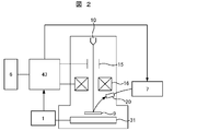
- FIG. 2 is a longitudinal sectional view showing the configuration of the inspection apparatus of this embodiment.
- the inspection apparatus includes an electron gun 10, an electron beam scanning unit 15, a lens unit 16, a sample 9 as an object to be detected (observed object), a stage 31, a stage control unit 1, a detection unit 20, an image.
- the processing unit 7, the scanning control unit 43, the apparatus control unit 6, and a monitor 50 are included.
- an electron beam generated from the electron gun 10 is swung at an appropriate angle by the electron beam scanning unit 15, and the electron beam is focused by the lens unit 16, so that an appropriate scanning condition on the sample 9 is obtained.
- scanning in a certain direction for example, the X direction under conditions such as scanning interval, scanning speed, beam spot diameter, and the like
- the line image in the X direction obtained by the detection unit 20 and the image processing unit 7 is, for example, on the stage 31.
- the XY plane images are continuously displayed in the Y direction while being shifted in the Y direction, and an XY plane image is displayed on the monitor 50.
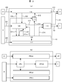
- the scanning control unit 43 is roughly divided into a scanning position calculation unit 118, a scanning control unit 120, a programmable sequencer 109, and a synchronization signal generation unit 119.
- the scanning position calculation unit 118 receives position information (X, Y coordinate values) 200 of the stage on which the sample is mounted from the stage 31, and is a control signal to the electron beam scanning unit 15 based on the position information 200.
- the deflection amount 213 is calculated and output.
- the scanning position calculation unit 118 receives a scanning line reference coordinate 203 that is a reference position of a line to be scanned from a scanning control unit 120 described later, and calculates a residual displacement 202 that is a difference amount between the position information 200 and the scanning line reference coordinate 203. .
- the residual displacement 202 is a reference deflection amount indicating how much the electron beam needs to be deflected in order to scan the reference coordinates of the target scanning line with respect to the stage position.
- the scanning line reference coordinates 203 normally indicate the center coordinates of the scanning line, but may be an end of the scanning line or an arbitrary coordinate (pixel pitch unit) on the scanning line.
- the scanning position calculation unit 118 calculates a deflection amount 213 in which a pixel coordinate 212 indicating which pixel in the target scanning line is scanned is added to the residual displacement (deviation amount) 202 that is a reference deflection amount of the target scanning line. calculate. That is, the scanning position calculation unit 118 calculates the deflection amount for controlling the scanning position of the electron beam by converting the residual displacement (shift amount) into pixels.
- the pixel coordinates 212 are generated by a programmable sequencer 109 and a pixel coordinate generation unit 113, which will be described later. For example, if the pixel coordinates are incremented in the range of ⁇ 512 to +511, 1024 pixels centering on the reference coordinates 203 of the scanning line. It is possible to scan long lines.
- the scanning control unit 120 is a beam scanning scheduling unit in this embodiment.
- the scanning control unit 120 is a part that controls the above-described scanning position calculation unit 118, a synchronization signal generation unit 119, which will be described later, and the programmable sequencer 109 (for example, for the scanning position calculation unit 118, the reference coordinates of the scanning line). (Schedule of electron beam scanning is notified by sequentially transmitting 203). More specifically, the scanning control unit 120 calculates the scanning line reference coordinates 203 in units of lines (or units of combinations of a plurality of lines), generates the line unit synchronization signal 214, and sets the scanning cycle of the electron beam 19. Make adjustments.
- the scanning control unit 120 receives information from the apparatus control unit (host computer) 6 on what schedule (electron beam scanning condition 231) the electron beam scanning is performed in order to execute various controls. (Parameter) is received.
- the scanning control unit 120 calculates the scanning line reference coordinates 203 in units of scanning lines based on the electron beam scanning condition 231 instructed by the apparatus control unit 6 (converts parameters acquired from the apparatus control unit 6 into information as coordinates). ).
- the scanning line reference coordinates 203 are stored in a FIFO (First In First Out) memory, and are transmitted to the scanning position calculation unit 118 in the stored order every time a line update command 215 is issued from the programmable sequencer 109 described later.
- the FIFO memory is provided in the FPGA.
- the scanning control unit 120 manages and adjusts the scanning cycle, and issues a cycle trigger 207 for instructing the start of scanning to the programmable sequencer 109 described later according to the scanning cycle.
- the programmable sequencer 109 controls the inspection apparatus so as to start line scanning in accordance with the issuance timing of the periodic trigger 207.
- a hardware timer (not shown) is used for managing and adjusting the scanning cycle. As long as the set scanning period 206 from the scanning control unit 120 is not changed, the hardware timer can continuously issue a period trigger having an accurate period. As a result, the line scanning is performed with a certain period extremely accurately.
- the scanning control unit 120 monitors the residual displacement 202 and adjusts the scanning cycle based on the progress of the residual displacement 202. For example, if the residual displacement 202 that is updated for each line scan increases, this means that the scanning cycle is slow with respect to the moving speed of the stage. In the scanning period as it is, the deflection amount 218 of the electron beam 19 increases too much and exceeds the deflectable range of the electron beam 19, so the scanning period is adjusted to be short. However, if the scanning period is changed rapidly, the irradiation time of the electron beam 19 on the sample 9 to be inspected changes, resulting in variations in the charged state, making it difficult to obtain a stable contrast. Therefore, the scanning control unit 120 performs follow-up control so that the change rate of the scanning cycle changes gently so as not to exceed a predetermined threshold value.
- the branch flag 209 is a flag indicating where to move the electron beam in order to scan the next scanning range after scanning a certain scanning range based on the electron beam scanning condition 231.
- the branch flag 209 is a means for changing a scanning sequence procedure by a programmable sequencer 109 described later based on an instruction from the scanning control unit 120.
- the branch flag 209 is also stored in the FIFO memory structure in the same manner as the scanning line reference coordinates 203 described above, and is transmitted to the programmable sequencer 109 in the stored order every time a line update command 215 is issued from the programmable sequencer 109 described later. Thereby, the scan sequence procedure can be changed for each scan line.
- the scanning direction when the scanning direction is to be switched alternately between the forward direction and the backward direction for each line, the scanning direction can be alternately switched by scheduling the scanning direction for each line as the branch flag 209, that is, storing it in the FIFO memory in the processing order. It becomes.
- the scanning control unit 120 generates a line unit synchronization signal 214 which is a scanning line unit synchronization signal 53 and a blanking signal 54.
- the synchronization signal 53 is means for synchronizing the secondary electron detection timing in the image processing unit 7 and the scanning timing of the electron beam 19 as a result of scanning of the electron beam 19.
- the line unit synchronization signal 214 is stored in the FIFO memory structure in the same manner as the scanning line reference coordinate 203, and is transmitted to the synchronization signal generation unit 119 in the stored order every time a line update command 215 is issued from the programmable sequencer 109 described later. Is done.
- the vertical direction of scanning of the synchronization signal 53 is called a V-Valid signal, and the horizontal direction is called an H-Valid signal.
- the blanking signal 54 is a means for controlling blanking by the electron beam scanning unit 15.
- the scanning control unit 120 needs to control each part in the scanning control unit 43 in a complicated manner based on the electron beam scanning condition 231 of the apparatus control unit 6, and is preferably configured by a microprocessor.
- the scan control processor is freed from control with a line scanning cycle shorter than the control cycle of the processor, so that the processing load is reduced as compared with the case where control is performed for each line. This leads to avoidance of scan cycle disturbance due to generation of dummy cycles, which is a characteristic of the processor, in addition to the merit in terms of cost and labor saving in which a smaller and slower processor can be used.
- the programmable sequencer 109 performs various controls such as pixel coordinates and synchronization signals that change within one scanning line based on the scanning cycle adjusted by the scanning control unit 120 in units of scanning lines (or units of combinations of a plurality of scanning lines). Do.
- the programmable sequencer 109 is accompanied by an instruction memory 117 and a pixel coordinate generation unit 113.
- the programmable sequencer 109 sequentially reads a microprogram which is a combination of microinstructions (test patterns) stored in the instruction memory 117, and updates the scanning line reference coordinates 203 and the line unit synchronization signal 214 of the scanning control unit 120 according to the microinstructions.
- a line update command 215 that triggers scanning a cycle update command 211 that prompts adjustment of the scanning cycle managed by the scanning control unit 120, and pixel coordinates that specify pixel coordinates to be scanned to the pixel coordinate generation unit 113 described later
- the timing of the command 219 and the pixel unit synchronization signal 216 that changes within one scanning line is controlled.
- a program control instruction for generating a read address of the next microprogram in addition to each function block control instruction such as the line update instruction 215, a program control instruction for generating a read address of the next microprogram, a repetitive instruction for realizing repetitive processing such as a loop, etc.
- program control instructions there are program control instructions.
- the programmable sequencer 109 can execute various programs such as conditional branching based on the branch flag 209 and repeated loops.
- Programmable sequencer 109 specializes in electron beam scanning control, and can be configured with a simple instruction execution circuit compared to general-purpose processors, enabling operation at several hundreds of MHz even with inexpensive FPGAs (Field Programmable Gate Array). It is. Furthermore, the microinstruction is composed of a plurality of bit fields corresponding to the type of instruction, and is processed by a functional block corresponding to each bit field. Therefore, if the microinstruction is an instruction for another functional block, it can be executed in parallel. The programmable sequencer 109 can realize high-speed scanning control in units of clock cycles at a low cost.
- the instruction memory 117 is a memory block that stores a microprogram. Normally, it is possible to switch to scanning control corresponding to the scanning conditions by storing a plurality of patterns of microprograms and selecting a microprogram to be executed in accordance with the electron beam scanning conditions 231. Furthermore, the instruction memory 117 is configured to be rewritable from the apparatus control unit 6, and the microprogram can be rewritten in accordance with the newly proposed electron beam scanning condition 231.
- the pixel coordinate generation unit 113 is a means for calculating the coordinates of the pixel that irradiates the electron beam 19 as local coordinates in the scanning line.
- the calculation condition is determined by a pixel coordinate command 219 read from the instruction memory 117.
- the pixel coordinate generation unit 113 includes several register files and can be used as an operand of the pixel coordinate instruction 219.
- the pixel coordinate command 219 includes a value load from a register file, an addition process between register files, and the like, and the pixel width and line width can be switched depending on scanning conditions without rewriting the instruction memory 117. it can.
- the programmable sequencer 109 can control the synchronization signal 53 and the blanking signal 54 with higher accuracy in units of pixels by controlling the pixel unit synchronization signals 216 that change in the scanning line. Since the scanning control unit 120 does not control which pixel is irradiated with the electron beam, this pixel unit synchronization signal 216 is required when it is desired to synchronize the pixel unit. Note that whether to synchronize in line units or pixel units is given by the device control unit 6.
- the pixel unit synchronization signal 216 is generated based on a microprogram (test pattern).
- the synchronization signal generation unit 119 is a unit that selects the line unit synchronization signal 214 generated by the scanning control unit 120 and the pixel unit synchronization signal 216 generated by the programmable sequencer 109.
- the synchronization signal 53 and the blanking signal 54 are controlled by the pixel unit synchronization signal 216.
- the line unit synchronization signal 214 is used.
- the synchronization signal 53 and the blanking signal 54 are controlled.
- the hardware configuration diagram corresponding to the functional block diagram of the scanning control unit 43 described with reference to FIG. 3A is shown in FIG.
- the scanning position calculation unit 118, the pixel coordinate generation unit 113, the synchronization signal generation unit 119, and the programmable sequencer 109 are configured by an FPGA, and the instruction memory 117 and the scanning control unit 120 are configured by a memory and a CPU, respectively.
- the CPU and the memory are often incorporated in the FPGA, and the three FPGAs shown in FIG. 3B are often realized by a single FPGA.
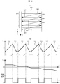
- FIG. 4 is a diagram illustrating a first embodiment of the operation of the inspection apparatus according to the present embodiment.
- FIG. 4A shows a state in which the inspection stripe 300 is scanned in a certain direction (forward direction) in order from the top for each line pitch 301.
- 4B shows the transition of the deflection voltages Vx and Vy of the electron beam scanning unit 15 and the synchronization signal to the image processing unit 7 or the electron beam scanning unit 15 during scanning (in this case, the electron beam scanning). It is assumed that the part 15 is an electrostatic deflection system).
- the voltages Vx and Vy in FIG. 4B indicate changes in the deflection voltage in the x and y directions applied to the electron beam scanning unit 15 when the sample stage is not moved. May be moved in the y direction (the same applies to Vy in FIGS. 5 to 17).
- the scanning (moving) in the y direction is not performed (Vy is constant) while the electron beam 19 is scanned in the x direction (during the ramp waveform in which Vx rises to the right and falls to the right).
- Vy is constant
- the electron beam 19 may be scanned in the ⁇ x directions while moving the sample stage in the y direction (the same applies to the following embodiments).
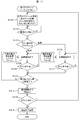
- FIG. 7 and 8 are flowcharts for explaining the operation of the scanning control unit 43 for realizing the scanning method shown in FIG.
- FIG. 7 shows an operation flow of the scanning control unit 120
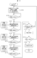
- FIG. 8 shows an operation flow of the programmable sequencer 109.
- the flow of the scan control processor shown in FIG. 7 is composed of three processes: a scan (scan) start process, an interrupt process, and a scan end process.
- the scanning control unit 120 sets the scanning line reference coordinates 203 in the inspection stripe 300 to the scanning condition 231. (Step S701). At the same time, the scanning control unit 120 generates a line unit synchronization signal 214 that is a synchronization signal that changes for each line (step S701). The process in step S701 is continued until the batch line scheduling is completed (step S702).
- the scan controller 120 notifies the completion of the scan schedule, whereby the programmable sequencer 109 is activated (step S703), and deflection control of one scan line shown in FIG. 8 to be described later is started.
- the subsequent flow of FIG. 7 and the flow of FIG. 8 are executed in parallel.
- the scanning control unit 120 monitors the residual displacement 202 in order to determine whether or not the first scanning line has reached a scannable position by moving the stage (step S704).
- the scanning control unit 120 sets a timer for the subsequent line scanning period (step S705). Thereafter, the scanning control unit 120 starts a timer and simultaneously issues a periodic trigger 207 to notify the programmable sequencer 109 of the arrival of the first scanning line (step S706).
- the first scan line arrives when the residual displacement becomes zero, that is, the stage coordinates reach the target scan line coordinates, but this inspection apparatus can also scan in the y direction. Therefore, it is possible to provide a threshold value for the residual displacement and to start scanning before the stage coordinates reach the target scanning line coordinates.
- the scan control unit 120 supplements the information of the scan line reference coordinates 203 and the line unit synchronization signal 214 each time an interrupt (period update command 215) is applied from the programmable sequencer 109 (step S711). ).
- the process in step S711 is continued until the batch line scheduling is completed (step S712).
- Such information supplement (interrupt) processing is necessary because the number of scan lines that can be stored in each storage unit is generally smaller than the number of scan lines of the inspection stripe due to hardware resource limitations.
- interrupt processing is not necessary if all information is set for the range to be scanned.
- the scanning control unit 120 also corrects the line scanning cycle at the same time (step S713).
- the line scanning cycle after the forced cycle trigger 207 is issued is strictly periodically issued by the hardware timer. Thereby, it is possible to reduce as much as possible the variation in the charged state caused by the electron beam scanning time that causes the variation in the detection contrast.
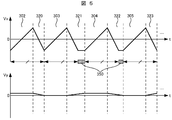
- FIG. 5 shows a state in which the application time of the electron beam changes due to variations in the scanning cycle according to the conventional method.
- the scanning cycle is basically managed at a constant cycle by a hardware timer, but the stage moving position fluctuates and the stage position deviates from the scannable range, or as shown in FIG.
- the line scanning cycle may be made variable, for example, when the scanning cycle is changed intentionally.
- the inspection apparatus includes means for correcting the line scanning cycle by the interruption processing of the scanning control unit 120. Thereby, it is also possible to change the line scanning cycle for every fixed number of lines.
- the scanning control unit 120 does not require a high-performance processor because it does not require control for each line scanning cycle, which is a relatively short cycle as a control cycle of the processor. This is advantageous in terms of radiation noise because there is no need for operating the processor with a high-speed clock due to cost reduction due to circuit scale reduction or the like. Further, since the scanning cycle does not depend on the performance of the processor, it is relatively easy to shorten the scanning cycle, and there is an effect of suppressing variations in the scanning cycle due to the dummy cycle of the processor.
- the scanning control unit 120 instructs the programmable sequencer 109 to stop scanning (step S721), and waits until the programmable sequencer 109 stops (step S722).
- the scanning control unit 120 executes end processing (step S723).
- the termination process includes, for example, control to reset the scanning line reference coordinates 203 and the line unit synchronization signal 214, and the like.
- FIG. 8 is a flowchart for explaining the operation of the programmable sequencer 109.
- the instruction memory 117 a microprogram for realizing the processing of the flowchart is downloaded in advance from the apparatus control unit 6 before scanning is started.
- the instruction memory 117 has a rewritable configuration, and can be corrected at any time as the operation flow is changed. As a result, various scanning methods can be realized and changed online.
- the programmable sequencer 109 updates the next scan line reference coordinate 203, the line unit synchronization signal 214, and the branch flag 209 stored by the scan control unit 120 as the scan line reservation information by the line update command 215 (step S802).
- the programmable sequencer 109 is configured to execute each instruction in parallel as necessary. Therefore, the programmable sequencer 109 can control hardware resources in real time without a dummy cycle, and can prevent a waiting time unnecessary for scanning from being inserted and manage a strict scanning cycle.
- the programmable sequencer 109 detects the periodic trigger 207 (step S803), an actual scanning process is performed using the periodic trigger 207 as a reference point.
- the scanning process first, the pixel coordinate command 219 is interpreted by the pixel coordinate generation unit 113, and the pixel coordinates 212 in the scanning line are generated one after another (step S807).
- the pixel coordinates 212 are referred to by the scanning position calculation unit 118, and a deflection amount 213 that determines the scanning coordinates of each scanning pixel is calculated.
- the pixel coordinate generation unit 113 includes a register file that stores a plurality of pieces of pixel pitch information.
- Pixel pitch information is loaded from an arbitrary register file by the pixel coordinate command 219, and when the pixel coordinate command 219 is further executed, pixel coordinate calculation is performed from the loaded pixel pitch information.
- pixel coordinates are calculated at every pixel pitch from the left end to the right end of each forward scan 302, 303, 304, and 305.
- the pixel pitch information stored in the register file can be arbitrarily rewritten when the instruction memory 117 is rewritten, and the designation of reference destinations from a plurality of register files can be selected as an argument by the pixel coordinate instruction 219 which is a microinstruction. It has become a structure. For this reason, scanning with an arbitrary pixel pitch is possible in accordance with the scanning condition 231.
- step S808 the programmable sequencer 109 determines whether one line scan is completed. If not completed, the scanning is continued. If completed, the process proceeds to step S810.
- step S810 it is determined whether or not scanning of the planned number of lines has been completed using a repetitive command. This is intended to prompt the scanning control unit 120 to update the subsequent scanning line schedule.
- the period update command 211 is applied to the scanning control unit 120 (step S811).
- the programmable sequencer 109 determines whether there is a next line to be scanned (step S812).
- the scanning control unit 120 that has received the cycle update command 211 (interrupt request) performs the supplementation of the scanning line reference coordinates 203 and the line unit synchronization signal 214 and the adjustment of the scanning cycle. Become. If there is no line to be scanned, the programmable sequencer 109 performs scanning end processing (step S813).
- the scan control unit 120 corrects the scan cycle in the interrupt process in order to cope with the case where the scan cycle is intentionally corrected for the stability of the system or experimental meaning.
- the number of repetitions here corresponds to the line number interval for scanning period correction.
- the programmable sequencer 109 performs high-speed line scanning by the microprogram stored in the instruction memory 117. That is, various scanning sequences can be realized by rewriting the microprogram of the instruction memory 117.
- Example 2 In the present embodiment, as an example of a scan sequence that can be realized by rewriting a microprogram, a back scan and a back precharge scan will be described. Since the overall configuration of the apparatus is the same as that of FIG. 2 and FIGS. 3A and 3B described in the first embodiment, description thereof will be omitted.
- FIG. 9A shows an example of a scanning sequence in which scanning in the forward direction and scanning in the backward direction are alternately performed. Scanning not only in the forward direction but also in the backward direction in this way is highly effective in improving inspection throughput.
- FIG. 9B shows the transition of the deflection voltages Vx and Vy of the scanning deflector 15 and the synchronization signal to the image processing unit 7 or the electron beam scanning unit 15 during the reciprocating scanning. The difference from FIG. 4B is that since the backward direction is also used for scanning, the scanning cycle is strictly managed even during the backward direction scanning, and the synchronization signal is generated also during the backward scanning. .
- FIG. 10A shows an example in which the scan in the backward direction is used for the precharge scan.
- Performing the precharge scan before the actual scan is extremely effective in terms of stabilizing the charging property, and further, a reduction in throughput can be suppressed as much as possible by applying the backward scan to the precharge scan.
- FIG. 10B shows the transition of the deflection voltages Vx and Vy of the electron beam scanning unit 15 and the synchronization signal to the image processing unit 7 or the electron beam scanning unit 15 during forward normal scanning and backward precharge scanning. . Since the precharge scan that is the return path is performed before the normal scan that is the outbound path, the process starts from the return path scan. Further, since the same line is scanned in the forward path and the backward path, the deflection voltage Vy changes every two lines. Further, since secondary electrons are not detected in the precharge scan, the synchronization signal is generated only during the forward scan.
- FIG. 11 is a flowchart for explaining the operation of the programmable sequencer 109 for realizing the scanning shown in FIGS. 9 and 10.
- the microprogram (test pattern) for this flowchart is downloaded from the apparatus control unit 6 to the instruction memory 117 in advance.
- the instruction memory 117 can be rewritten for each scan, but if the instruction memory 117 has a capacity capable of storing a plurality of microprograms, the plurality of microprograms are divided and arranged in the instruction memory 117.
- a configuration is also possible in which the microprogram instruction call address 221 is changed only for each scanning sequence.
- step S1101 to S1103 is the same as the processing from step S801 to S803 in FIG.
- step S1107 the programmable sequencer 109 checks the branch flag 209 for each line. That is, in the operation of the programmable sequencer 109 in this example, the path is branched by the branch flag 209 between the forward path process and the backward path process.
- the branch flag 209 is scheduled for each scan line by the scan control unit 120, and the programmable sequencer 109 reads the branch flag 209 for the corresponding scan line from the branch flag storage unit 112 by the line update command 215 at the start of the line.
- the forward scan and the backward scan are alternately scheduled by alternately scheduling the branch flag 209 for selecting the forward flow and the branch flag 209 for selecting the backward flow. Can be performed.
- the processing after starting the forward and backward scanning processing is the same as the processing of FIG.
- the difference between the scanning direction of the forward scanning and the backward scanning and the pixel information can be dealt with by preparing a plurality of register files of the pixel coordinate generation unit 113.
- the forward path and the backward path are provided in the pixel coordinate register file of the pixel coordinate generation unit 113 used in the pixel coordinate command 219, respectively.
- the backward scanning can be realized by setting the pixel pitch to a negative value.
- step S1113 when the repeated line number scanning is not completed, the process proceeds to step S1107.
- Example 3 black belt scanning will be described.
- the scanning method there is a scanning method in which an electron beam non-irradiation region is provided at one or both of the start point and the end point of the scan line, which is called black belt scanning in this embodiment.
- the overall configuration of the apparatus is the same as that shown in FIG. 2 and FIGS.
- FIG. 12 and 17 are diagrams for explaining an example of black belt scanning.
- FIG. 12 shows a scanning method in which each line scan is performed only in the forward scan as in the above-described basic scan and interval variable scan, but the areas of the first few pixels and the last few pixels of the scan line are shown.
- FIG. 12B shows the timing of the electron beam blanking signal 54 in addition to the Vx and Vy voltages and the synchronization signal 53.
- the synchronization signal 54 in FIG. 12B is effective in synchronization with the slopes of the deflection voltages Vx and Vy, but the blanking signal 54 is invalid on the inner side of the scanning line compared with the synchronization signal 53 (that is, electronic). Line is ON).
- an electron beam non-irradiation region is formed at the beginning (upper end) and the end (lower end) of the electron beam, and an electro-optically unstable portion is removed from the image signal to prevent deterioration of the inspection performance. be able to.
- extra electron beam irradiation on the sample is cut.
- the size of the non-irradiation region can be controlled by controlling the falling or rising timing of the blanking signal with respect to the rising or falling timing of the synchronization signal.
- FIG. 13 is a flowchart for explaining the operation of the programmable sequencer 109 for realizing the black belt scanning shown in FIG.
- the processing sequence of FIG. 13 is the same as the processing shown in FIG. 8, but the following processing is different. That is, the scanning line is divided into three sections, a leading blank area 316, a beam ON area 317, and a trailing blank area 318, and a register file of pixel coordinates 212 is provided for each scanning section, and a scanning loop of each section is provided. 8 is different from FIG. 8 in that it is realized by sequentially processing. In addition, the synchronization signal 53 and the blanking signal 54 in each section are controlled by the pixel unit synchronization signal 216.
- the pixel coordinate command 219 and the register file accompanying the pixel coordinate command 219 can be switched in units of pixel clocks, and similarly, a unit that can control the synchronization signal 53 and the blanking signal 54 in units of pixels is provided.
- the scanning method including control of the synchronization signal 53 and the blanking signal 54 in units can be switched.
- the back scan, the back precharge scan, and the black belt scan have been described as examples of the scan sequence, but various other scan sequences can be realized by rewriting the microprogram of the instruction memory. It is possible. Needless to say, combinations of scans of the back scan, the back precharge scan, and the black belt scan can also be realized.
- Example 4 In the present embodiment, a configuration example of an operation screen GUI (Graphical User Interface) commonly used in the charged particle beam apparatuses described in the first to third embodiments will be described.
- GUI Graphic User Interface
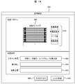
- FIG. 14 is a diagram illustrating an example of a GUI according to the present embodiment. As shown in FIG. 14, an example in which the scanning function selection unit of the present embodiment is provided in the display unit 500 so that the user can select various conditions with good visibility and operability (input screen of the monitor 50 ( GUI)).
- GUI input screen of the monitor 50
- the user uses this GUI to select the scan method with the input means 540. This may be selected from a pull-down menu. As a result, the user can select a scanning method only in one direction (one swing), a scanning method in both directions with a swing back (both swing), and the like.
- the input means 510 determines the role of reversal in the scan method that performs reversal. In other words, the user selects whether to obtain the inspection image data (inspection) or use it for precharge (PC) or discharge (DC) by turning back.
- the input unit 530 sets other conditions (such as the number of reciprocating scans).
- the scanning method may include means that allows the user to arbitrarily modify the scanning display 560.
- an inspection index display 570 for displaying the quality of the inspection determined by the scanning displayed on the scanning display 560 and the index amount related to the inspection throughput.
- charging stability and scanning period at each scanning are displayed as an index related to inspection quality
- an inspection speed is displayed as an index related to inspection throughput.
- the input means 540, 510, and 530 are shown here, it is not necessary to equip them all, and the present invention is not limited to this.
- the apparatus control unit 6 is provided with a plurality of microprograms and register file data that meet selectable scanning conditions.
- the microprograms and register file data according to the scanning conditions are designated. Are written into the instruction memory 117 of the scanning control unit 43 and the register file of the pixel coordinate generation unit 113.
- a microprogram can be arbitrarily rewritten.
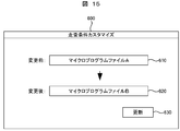
- a scanning condition customization screen 600 shown in FIG. 15 is displayed.
- the user can designate a data file of an arbitrary microprogram by the file name designation means 620 after the change, and can rewrite the contents of the instruction memory 117 by the update means 630.
- the changed scanning conditions are displayed on the scanning display 560, and the changed contents can be visually confirmed.
- this embodiment can also be realized by a program code of software that realizes each function.
- a storage medium in which the program code is recorded is provided to the system or apparatus, and the computer (or CPU or MPU) of the system or apparatus reads the program code stored in the storage medium.
- the program code itself read from the storage medium realizes the functions of the above-described embodiment, and the program code itself and the storage medium storing the program code constitute this embodiment.
- a storage medium for supplying such program code for example, a flexible disk, CD-ROM, DVD-ROM, hard disk, optical disk, magneto-optical disk, CD-R, magnetic tape, nonvolatile memory card, ROM Etc. are used.
- an OS operating system
- the CPU of the computer or the like performs part or all of the actual processing based on the instruction of the program code. You may make it implement
- the program code of the software that realizes the functions of the embodiments via a network, it is stored in a storage means such as a hard disk or memory of a system or apparatus or a storage medium such as a CD-RW or CD-R And the computer (or CPU or MPU) of the system or apparatus may read and execute the program code stored in the storage means or the storage medium when used.
- a storage means such as a hard disk or memory of a system or apparatus or a storage medium such as a CD-RW or CD-R
- the computer (or CPU or MPU) of the system or apparatus may read and execute the program code stored in the storage means or the storage medium when used.
- an inspection apparatus using a scanning electron microscope has been described as an example.
- an apparatus that scans a charged particle beam to acquire an image for example, an SEM type defect review apparatus, an SEM
- the present invention can be applied to an apparatus such as a type length measuring device, a scanning electron microscope or a scanning ion microscope.
Landscapes
- Chemical & Material Sciences (AREA)
- Analytical Chemistry (AREA)
- Testing Or Measuring Of Semiconductors Or The Like (AREA)
- Analysing Materials By The Use Of Radiation (AREA)
Abstract
本発明の荷電粒子線装置は、入力される走査条件に基づいて、ビーム走査をスケジューリングするビーム走査スケジューリング手段(120)と、ビーム走査スケジューリング手段によって生成されたビーム走査スケジュールに従って、ビーム走査制御を行うプログラマブルシーケンサ(109)とを備える。走査スケジューリング手段は、走査条件に基づいて、走査ライン単位での走査ライン基準座標(203)を算出し、走査周期トリガ(207)を発行する。プログラマブルシーケンサは、ライン走査手順情報及び走査スケジューリング手段から与えられる走査周期トリガに基づいて、走査ライン基準座標の供給のタイミング及びライン内画素単位での走査位置を制御する。 これにより、多様な走査シーケンスを、その検査条件に応じて柔軟に変更可能とすると同時に、帯電の安定化の妨げとなる走査周期のばらつきを極力排除し、安定した走査周期でビーム走査を行う検査装置を提供することが可能になった。
Description
本発明は、荷電粒子線を走査して電子画像を得る荷電粒子線装置に関する。例えば、微細なパターンを有する半導体装置,基板,フォトマスク(露光マスク),液晶等の試料の測定・検査に用いられる検査装置,計測装置,観察装置,走査電子顕微鏡あるいは走査イオン顕微鏡などが該当する。
半導体素子(装置)の製造過程において、リソグラフィー処理,エッチング処理、及びその他の処理における異常発生や不良発生を、早期に、あるいは、事前に検知するために、各製造工程の終了時に半導体ウェハ上のパターンの検査が実施されている。
回路パターンの微細化や回路パターン形状の複雑化,材料の多様化に伴い、光学画像よりも分解能の高い電子線画像を用いて、パターンを検査する方法及び装置が実用化されている。
ウェハの口径増大と回路パターンの微細化に追随して高スループット且つ高精度な検査を行うためには、非常に高速に、高SNな画像を取得することが重要となる。
特許文献1には、ビーム走査を高速かつ高精細に行うために、走査偏向制御を高速回路と低速回路で分割して処理し、高速回路と低速回路間のデータ受け渡しや同期方法を工夫することで、高速で高精度なデータ演算処理を可能とした発明が開示されている。
ここで、電子線画像を得るために検査対象に電子線を照射することにより検査対象が帯電(チャージアップ)するが、帯電状態によっては、電子線による検査で安定した輝度の画像を得ると共に、所定の検査精度を得ることが困難になる場合がある。
検査対象における帯電が発生すると、発生部分からの二次電子発生効率が低下したり、発生した後の二次電子の軌道が影響を受けたりして、画像の明暗が変化してしまうと同時に、画像が実際の回路パターンの形状を反映せず歪んでしまうという問題がある。
更に、この帯電状態は、電子線の照射条件に敏感であり、電子線の照射速度や照射範囲を変えると同一箇所の同一回路パターンでもまったく異なるコントラストを持った画像となってしまう。
従来のSEMのように電子線電流の少ない細く絞った電子線を試料にゆっくり照射し、信号検出も長時間かけて行う場合、比較検査に必要なSN比を得るために、単位画素あたりの検出時間に検出された信号を積分して該単位画素の画像信号とする。既に述べたように、帯電は照射時間によって経時的に状態が変わるため、積分している間の画像信号が変化し、安定したコントラストを得ることが困難である。帯電による経時変化の影響を抑制する必要がある。
図1は、電子線19の走査時間および待ち時間とX方向の位置との関係を示す図である。図1において、走査時間T1は走査(1)と走査(2)の照射間隔とし、走査時間T2は走査(2)と走査(3)の照射間隔とされている。走査時間T3を固定的に制御するとき、T1とT2が同じ時間になるように走査することで、照射毎の待ち時間T4とT5を均一にする。このように照射間隔を一定にすることにより、帯電状況を均一にし、コントラスト斑の発生を抑えることができる。
また、Y偏向量を一定にすることにより、Y方向への偏向による焦点歪みなどの補正処理や、偏向視野外判定の処理などが不要になり、処理の簡素化により信頼性および処理速度を向上しスループット向上に寄与することが可能となる。
上記従来技術の何れのSEM式検査装置や検査方法においても、電子線ビームを利用するその性質から、SNを向上し、帯電やドーズ量の安定化を図り、かつ、検査スループットの低下を防止するため、ビーム走査方法や走査周期等を、検査対象や検査条件によって調整する方法が採られている。すなわち、ビーム走査時間を厳密に管理し、且つ、様々なビーム走査方法に対応する高い走査柔軟性を持ったビーム制御技術が求められている。
しかしながら、実際に、ビーム走査時間を厳密に管理し、且つ、様々なビーム走査方法に対応する高い走査柔軟性を持ったビーム制御を実現するには、以下のような問題がある。
通常、様々なビーム走査方法に対応する手段としてマイクロプロセッサを使用して、走査シーケンスを制御する方法が考えられる。ところが、マイクロプロセッサはソフトウェア上に様々な走査シーケンスを用意することが容易である反面、制御時間を厳密に管理することは困難である。特に、ビーム走査は通常、数ナノ秒のクロックサイクルで制御されるため、ダミーサイクルの存在するマイクロプロセッサで1サイクル単位の管理は困難である。ビーム走査シーケンスを単純にマイクロプロセッサが管理することは、走査周期に揺らぎを発生させる原因となる。制御周期の揺らぎは、ビーム走査時の走査部位の帯電均一性を損なう他、ビーム走査を制御するアナログ信号にジッタを発生させ、検出感度を低下させる。なお、処理能力の高い、高価なプロセッサを用いれば、ある程度上述のような問題は解決できる可能性はあるが、コストが過大になってしまう。よって、プロセッサの性能に左右されずに走査周期を安定させることのできる方法が望まれる。
一方、ビーム走査周期を厳密に管理することを目的としてビーム走査制御を回路にて行う場合、様々なビーム走査方法に対応することが困難になる。ビーム走査方法毎に回路を用意することも考えられるが、回路構成の大規模化及び複雑化を伴い、高価格になってしまう。また、ビーム走査の最適方法は、検査対象や検査条件により異なるため、新しい走査方法が確立されるたびに回路を再構築することは現実的でない。よって、プロセッサを用いることが必要となってくる。
本発明はこのような問題に鑑みてなされたものであり、ビーム走査周期が安定となるように管理しつつ、多様なビーム走査を実現することのできる電子線走査制御の構成を提供するものである。
発明による荷電粒子線装置では、荷電粒子線装置の走査制御を、走査ライン単位の制御と、1つの走査ラインを精密に走査させるための制御とに分業して実行することにより、上記の課題を解決する。上記「分業して実行する」という技術思想を具現化する一つの構成として、本発明の荷電粒子線装置は、走査ライン単位のビーム走査を制御するビーム走査スケジューリング手段と、当該ビーム走査スケジューリング手段によって生成されたビーム走査スケジュールに従って、ビーム走査制御を行うプログラマブルシーケンサとを備える。プログラマブルシーケンサにより走査ライン1本の制御を行うことにより、1つの走査ラインの制御を従来よりも非常に精密に実行することが可能となる。
さらなる本発明の特徴は、以下本発明を実施するための最良の形態および添付図面によって明らかになるものである。
本発明によれば、SNの向上や偏向歪の除去等の検出感度を向上させるために必要となる多様な走査シーケンスを、その検査条件に応じて柔軟に変更可能とすると同時に、帯電の安定化の妨げとなる走査周期のばらつきを極力排除し、安定した走査周期でビーム走査を実現できる。
また、走査シーケンスを可視化する手段を設けることによりカスタマイズ性及び操作性の向上を実現できる。
以下、添付図面を参照して本発明の実施形態について説明する。ただし、本実施形態は本発明を実現するための一例に過ぎず、本発明の技術的範囲を限定するものではないことに注意すべきである。また、各図において共通の構成については同一の参照番号が付されている。
まず初めに、各実施例に共通する基本構成について説明する。上述の通り、本発明の一形態では、荷電粒子線装置のビーム走査制御手段が、ビーム走査スケジューリング手段とプログラマブルシーケンサとを備える。走査スケジューリング手段は、走査条件に基づいて、走査ライン単位での走査ライン基準座標を算出し、走査周期トリガを発行する。プログラマブルシーケンサは、予め内部メモリに格納されているライン走査手順情報及び走査スケジューリング手段から与えられる走査周期トリガに基づいて、走査ライン基準座標の供給のタイミング、及びライン内画素単位での走査位置を制御する。ライン走査手順情報は、各走査ラインをライン単位で制御するための制御情報であり、例えば、1ライン画素数,ライン走査繰り返し回数,画素ピッチ,ライン走査方向の情報を含んでいる。1ライン画素数は1ラインあたりの画素数にあたり、1ライン走査の完了の判定に使用する。ライン走査繰り返し回数は、同一処理内容のライン走査を繰り返す回数にあたり、複数ライン走査の完了の判定に使用する。画素ピッチは、画素間の距離にあたり、画素座標の変位量として使用する。ライン走査方向の情報は、ライン走査を正負何れの方向に行うかを判定するために使用する。ライン走査方向情報は画素ピッチ値の正負に代えても良い。
上記荷電粒子線装置は、さらに、信号検出器に対して同期信号を供給する同期信号出力手段を備える。この走査スケジューリング手段は、走査条件に基づいて、ライン単位同期信号を生成し、同期信号出力手段に供給する。そして、同期信号出力手段は、プログラマブルシーケンサから与えられるライン更新命令に基づいて、ライン単位同期信号を出力する。
また、プログラマブルシーケンサは、ライン走査手順情報に含まれる画素単位同期命令に基づいて、画素単位同期信号を生成して同期信号出力手段に供給する。そして、同期信号出力手段は、走査条件に基づいて、ライン単位同期信号及び画素単位同期信号の何れかを選択して出力する。
ライン走査手順情報は、ライン走査の繰り返し回数,画素ピッチ、及びライン走査方向の情報を複数含んでいる。この場合、プログラマブルシーケンサは、走査条件によってライン走査の繰り返し回数,画素ピッチ、及びライン走査方向を、走査シーケンスごとに切り替えるようにする。
上記荷電粒子線装置は、さらに、走査条件を入力し、走査条件に基づいて決定された走査スケジュールの内容を表示画面に表示して確認可能とするための確認手段と、走査スケジュールに基づいて実行される走査シーケンスを視覚的情報として生成する手段と、を備える。また、確認手段は、生成された走査シーケンスの視覚的情報を前記表示画面に表示する。
上記荷電粒子線装置は、さらに、ライン走査手順情報を上位システムより書き換える手段を備える。走査条件毎に操作手順情報を切り替える。
〔実施例1〕
本実施例では、走査電子顕微鏡を応用した検査装置の実施例について説明する。図2は、本実施例の検査装置の構成を示す縦断面図である。この検査装置は電子銃10と、電子線走査部15と、レンズ部16と、被検出物(観察物)である試料9と、ステージ31と、ステージ制御部1と、検出部20と、画像処理部7と、走査制御部43と、装置制御部6と、モニタ50から構成されている。
本実施例では、走査電子顕微鏡を応用した検査装置の実施例について説明する。図2は、本実施例の検査装置の構成を示す縦断面図である。この検査装置は電子銃10と、電子線走査部15と、レンズ部16と、被検出物(観察物)である試料9と、ステージ31と、ステージ制御部1と、検出部20と、画像処理部7と、走査制御部43と、装置制御部6と、モニタ50から構成されている。
図2に示す検査装置においては、電子銃10から生成される電子線を電子線走査部15で適切な角度で振り、レンズ部16でその電子線をフォーカスして試料9上を適切な走査条件、例えば走査間隔,走査速度,ビームスポット径などの条件で、ある方向、例えばX方向に走査させ、検出部20及び画像処理部7に得られたX方向の線画像をステージ31にて、例えばY方向にずらしながら連続的にY方向に連結してX-Yの面画像をモニタ50に表示するものである。
<走査制御部の詳細>
次に、図3(a)に示す機能ブロック図を用いて走査制御部43の詳細について説明する。走査制御部43は、走査位置演算部118と走査制御部120とプログラマブルシーケンサ109と同期信号生成部119に大別される。
次に、図3(a)に示す機能ブロック図を用いて走査制御部43の詳細について説明する。走査制御部43は、走査位置演算部118と走査制御部120とプログラマブルシーケンサ109と同期信号生成部119に大別される。
1)走査位置演算部
まず、走査位置演算部118について説明する。走査位置演算部118は、ステージ31からの試料の搭載されたステージの位置情報(X,Yの座標値)200を受信し、位置情報200に基づいて電子線走査部15への制御信号である偏向量213を算出し、出力する。
まず、走査位置演算部118について説明する。走査位置演算部118は、ステージ31からの試料の搭載されたステージの位置情報(X,Yの座標値)200を受信し、位置情報200に基づいて電子線走査部15への制御信号である偏向量213を算出し、出力する。
走査位置演算部118は、後述の走査制御部120から走査するラインの基準位置である走査ライン基準座標203を受け取り、位置情報200と走査ライン基準座標203の差分量である残留変位202を算出する。残留変位202はステージ位置に対して目標とする走査ラインの基準座標を走査するために、どれだけ電子線を偏向させる必要があるかの基準偏向量となる。走査ライン基準座標203は通常、走査ラインの中心座標を示すが、走査ラインの端や、走査ライン上の任意の座標(画素ピッチ単位)でも良い。
走査位置演算部118は、目標走査ラインの基準偏向量である残留変位(ずれ量)202に対し、その目標走査ライン内のどの画素を走査するかを示す画素座標212を加味した偏向量213を算出する。つまり、走査位置演算部118は、残留変位(ずれ量)を画素換算して電子ビームの走査位置を制御するための偏向量を算出する。なお、画素座標212は後述のプログラマブルシーケンサ109、ならびに画素座標生成部113によって生成され、例えば、画素座標が-512~+511の範囲でインクリメントされれば、走査ラインの基準座標203を中心に1024画素長のラインを走査することが可能である。
2)走査ライン制御部(ビーム走査スケジューリング手段)
次に走査制御部120について説明する。走査制御部120は、本実施例におけるビーム走査スケジューリング手段である。走査制御部120は、前述の走査位置演算部118や、後述の同期信号生成部119,プログラマブルシーケンサ109を制御する部位である(例えば、走査位置演算部118に対しては、走査ラインの基準座標203を順次伝達することにより、電子ビーム走査のスケジュールを通知する)。より具体的には、走査制御部120は、ライン単位(或いは複数ラインの組合せ単位)での走査ライン基準座標203の算出、ライン単位同期信号214の生成を行うと共に、電子線19の走査周期の調整を行う。なお、走査制御部120は、様々な制御を実行するために、装置制御部(ホストコンピュータ)6から、どのようなスケジュール(電子線走査条件231)で電子ビームの走査を実行するかについての情報(パラメータ)を受け取る。ここで、走査周期とは、走査偏向信号波形の1周期と、波形間の電子ビーム照射しない待ち時間との和である。例えば、図1に示す鋸波波形の偏向信号で言えば、T1=T3+T4あるいはT2=T3+T5などである。
次に走査制御部120について説明する。走査制御部120は、本実施例におけるビーム走査スケジューリング手段である。走査制御部120は、前述の走査位置演算部118や、後述の同期信号生成部119,プログラマブルシーケンサ109を制御する部位である(例えば、走査位置演算部118に対しては、走査ラインの基準座標203を順次伝達することにより、電子ビーム走査のスケジュールを通知する)。より具体的には、走査制御部120は、ライン単位(或いは複数ラインの組合せ単位)での走査ライン基準座標203の算出、ライン単位同期信号214の生成を行うと共に、電子線19の走査周期の調整を行う。なお、走査制御部120は、様々な制御を実行するために、装置制御部(ホストコンピュータ)6から、どのようなスケジュール(電子線走査条件231)で電子ビームの走査を実行するかについての情報(パラメータ)を受け取る。ここで、走査周期とは、走査偏向信号波形の1周期と、波形間の電子ビーム照射しない待ち時間との和である。例えば、図1に示す鋸波波形の偏向信号で言えば、T1=T3+T4あるいはT2=T3+T5などである。
走査制御部120は、装置制御部6により指示される電子線走査条件231に基づき、走査ライン単位で走査ライン基準座標203を算出する(装置制御部6から取得したパラメータを座標に情報に変換する)。走査ライン基準座標203は、FIFO(First In First Out)メモリに格納され、後述のプログラマブルシーケンサ109からのライン更新命令215の発行毎に、格納した順序で走査位置演算部118に伝達される。図3(a)では明示されていないが、FIFOメモリはFPGA内に設けられている。
走査制御部120は、走査周期の管理・調整を行い、走査周期に従い、後述のプログラマブルシーケンサ109に対し、走査開始を指示する周期トリガ207を発行する。プログラマブルシーケンサ109は、この周期トリガ207の発行タイミングに合わせてライン走査を開始するように検査装置を制御する。通常、走査周期の管理・調整にはハードウェアタイマ(図示せず)を用いる。ハードウェアタイマは走査制御部120からの設定走査周期206が変更されない限り、正確な周期の周期トリガを連続して発行することができる。これにより、ライン走査は極めて正確に一定の周期で行われることになる。
走査制御部120は、残留変位202を監視し、残留変位202の経過に基づき走査周期を調節する。例えば、ライン走査毎の更新される残留変位202が拡大していくのであれば、ステージの移動速度に対し走査周期が遅いことを意味する。そのままの走査周期では電子線19の偏向量218が拡大しすぎて電子線19の偏向可能範囲を超えてしまうため、走査周期が短くなるように調節する。ただし、走査周期を急激に変化させると、電子線19の被検査試料9への照射時間が変化することにより帯電状態のばらつきが発生し、安定したコントラストを得ることが困難となる。そのため、走査制御部120は、走査周期の変化率が所定しきい値を超えないようなだらかに変化するように追従制御する。
分岐フラグ209とは、電子線走査条件231に基づいて、ある走査範囲を走査した後、次の走査範囲を走査するためにどの場所に電子線を移動させればいいかを示すフラグである。この分岐フラグ209は、後述のプログラマブルシーケンサ109による走査シーケンス手順を走査制御部120の指示に基づき変化させるための手段である。分岐フラグ209も前述の走査ライン基準座標203と同様に、FIFOメモリ構造に格納され、後述のプログラマブルシーケンサ109からのライン更新命令215の発行毎に、格納した順序でプログラマブルシーケンサ109に伝達される。これにより、走査ライン毎に走査シーケンス手順の変更が可能となる。例えば、走査方向をライン毎に往路方向,復路方向と交互に切り替えたい場合、分岐フラグ209として走査方向をライン毎にスケジューリング、すなわち処理順にFIFOメモリに格納することにより、走査方向の交互切り替えが可能となる。
さらに、走査制御部120は、走査ライン単位の同期信号53,ブランキング信号54であるライン単位同期信号214を生成する。同期信号53は電子線19の走査の結果、画像処理部7での二次電子検出タイミングと電子線19の走査のタイミングを連動させるための手段である。ライン単位同期信号214は、走査ライン基準座標203と同様に、FIFOメモリ構造に格納され、後述のプログラマブルシーケンサ109からのライン更新命令215の発行毎に、格納した順序で同期信号生成部119に伝達される。同期信号53の走査の垂直方向をV-Valid信号、水平方向をH-Valid信号と呼ぶ。また、ブランキング信号54は、電子線走査部15によるブランキングを制御するため手段である。
このように走査制御部120は、装置制御部6の電子線走査条件231に基づき、走査制御部43内の各部位を複雑に制御する必要があり、マイクロプロセッサにより構成することが望ましい。ただし本実施例の通り、予め走査するラインの座標をスケジュールしておくことで、以降のライン走査をプログラマブルシーケンサ109に任せることが可能となる。これにより、スキャン制御プロセッサとしてはプロセッサの制御周期に比べ短いライン走査周期での制御から開放されるため、1ライン毎の制御を行う場合に比べ処理負荷が軽減する。このことは、より小型化で低速なプロセッサを使用できるコスト面,省力化の面でのメリットの他に、プロセッサ固有の特性であるダミーサイクルの発生による走査周期の乱れの回避にも繋がる。
3)プログラマブルシーケンサ
次にプログラマブルシーケンサ109について説明する。プログラマブルシーケンサ109は、走査制御部120により調整される走査周期に基づいて、1走査ライン内で変化する画素座標,同期信号等の各種制御を、走査ライン単位(或いは複数走査ラインの組合せ単位)で行う。プログラマブルシーケンサ109には、インストラクションメモリ117,画素座標生成部113が付随する。
次にプログラマブルシーケンサ109について説明する。プログラマブルシーケンサ109は、走査制御部120により調整される走査周期に基づいて、1走査ライン内で変化する画素座標,同期信号等の各種制御を、走査ライン単位(或いは複数走査ラインの組合せ単位)で行う。プログラマブルシーケンサ109には、インストラクションメモリ117,画素座標生成部113が付随する。
プログラマブルシーケンサ109は、インストラクションメモリ117に格納されたマイクロ命令(テストパターン)の組合せであるマイクロプログラムを逐次読み出し、マイクロ命令に従って、走査制御部120の走査ライン基準座標203とライン単位同期信号214の更新を行うトリガとなるライン更新命令215と、走査制御部120で管理される走査周期の調整を促す周期更新命令211と、後述の画素座標生成部113に対し走査対象の画素座標を指示する画素座標命令219と、1走査ライン内で推移する画素単位同期信号216とをタイミング制御する。
代表的なマイクロ命令としては、ライン更新命令215等の各機能ブロック制御命令の他に、次のマイクロプログラムの読み出しアドレスを生成するためのプログラム制御命令,ループなどの繰り返し処理を実現する繰り返し命令等の、プログラム制御命令がある。プログラム制御命令により、プログラマブルシーケンサ109は、分岐フラグ209に基づく条件分岐や、繰り返しループなど多様なプログラム実行が可能である。
また、プログラマブルシーケンサ109は、電子線走査制御に特化しており、汎用プロセッサと比較して単純な命令実行回路で構成できるため、安価なFPGA(Field Programmable Gate Array)でも数百MHzの動作が可能である。更に、マイクロ命令は、命令の種類に応じた複数のビットフィールドから構成されており、各ビットフィールドに該当する機能ブロックで処理される。そのため、マイクロ命令は別の機能ブロック向けの命令であれば並列に実行することが可能である。プログラマブルシーケンサ109によって、クロックサイクル単位の高速な走査制御を安価に実現できる。
インストラクションメモリ117は、マイクロプログラムを格納するメモリブロックである。通常、マイクロプログラムを複数パターン格納しておき、電子線走査条件231に合わせ実行するマイクロプログラムを選択することで走査条件に応じた走査制御に切り替えることが可能となる。更に、インストラクションメモリ117は、装置制御部6から書き換え可能な構成となっており、新提案の電子線走査条件231に応じ、マイクロプログラムを書き換えることが可能である。
画素座標生成部113は、電子線19を照射する画素の座標を走査ライン内のローカルな座標として算出する手段である。算出条件はインストラクションメモリ117から読み出される画素座標命令219によって決まる。画素座標生成部113には、幾つかのレジスタファイルを備えており、画素座標命令219のオペランドとして使用できる。画素座標命令219には、レジスタファイルからの値のロード,レジスタファイル間での加算処理などが備えられており、インストラクションメモリ117を書き換えずとも走査条件による画素幅やライン幅の切り替えを行うことができる。
プログラマブルシーケンサ109は、走査ライン内で推移する画素単位同期信号216を制御することにより、画素単位でのより高精度な同期信号53,ブランキング信号54の制御を可能とする。走査制御部120は、どの画素に電子線を当てているかまでは制御していないので、画素単位で同期させたい場合には、この画素単位同期信号216が必要となってくるのである。なお、ライン単位及び画素単位のいずれで同期を取るかは、装置制御部6より与えられる。また、画素単位同期信号216は、マイクロプログラム(テストパターン)に基づいて生成されるものである。
4)同期信号生成部
続いて、同期信号生成部119について説明する。同期信号生成部119は、走査制御部120によって生成されるライン単位同期信号214と、プログラマブルシーケンサ109によって生成される画素単位同期信号216の選択を行う手段である。
続いて、同期信号生成部119について説明する。同期信号生成部119は、走査制御部120によって生成されるライン単位同期信号214と、プログラマブルシーケンサ109によって生成される画素単位同期信号216の選択を行う手段である。
通常、画素単位同期信号216により同期信号53及びブランキング信号54を制御するが、プリチャージスキャンやダミースキャンのように、ライン毎に同期信号を制御する必要がある場合、ライン単位同期信号214によって同期信号53及びブランキング信号54を制御する。このように同期信号53,ブランキング信号54の制御をライン毎と画素毎で分離することにより、高精度な同期信号の制御を可能にすると同時に、基本的な走査手順を変更せずに走査ラインの走査目的を変更することが可能となる。
以上、図3(a)を用いて説明した走査制御部43の機能ブロック図に対応するハードウェアの構成図を図3(b)に示した。走査位置演算部118,画素座標生成部113,同期信号生成部119およびプログラマブルシーケンサ109はFPGAによって構成され、インストラクションメモリ117および走査制御部120は、それぞれメモリ,CPUによって構成される。実際には、CPUとメモリはFPGAの中に組み込まれている場合が多く、また、図3(b)に示した3つのFPGAは単体のFPGAで実現されている場合も多い。
<走査制御の具体例>
以上、本実施例の検査装置の全体構成と、走査制御部43の構成について説明してきたが、以下では走査制御部43が実行する走査制御の具体例の一つとして、ラスタ走査およびその変形例としてのインターバル可変走査について説明する。なお、以下で参照する図4乃至図15において、実線の矢印は走査時のビーム移動方向を示し、破線の矢印はプリチャージ時あるいはディスチャージ時のビーム移動方向を示している。ここで、電子線ビーム照射による「ディスチャージ」とは、被検査試料が正に帯電している場合に電子線ビーム(電荷:負)照射により正帯電を除電することをいう。逆に、電子線ビーム照射による「プリチャージ」とは、被検査試料の帯電がゼロ又は負の場合に電子線ビーム(電荷:負)照射により負帯電状態にする、若しくは負帯電を強めることをいうものとする。
以上、本実施例の検査装置の全体構成と、走査制御部43の構成について説明してきたが、以下では走査制御部43が実行する走査制御の具体例の一つとして、ラスタ走査およびその変形例としてのインターバル可変走査について説明する。なお、以下で参照する図4乃至図15において、実線の矢印は走査時のビーム移動方向を示し、破線の矢印はプリチャージ時あるいはディスチャージ時のビーム移動方向を示している。ここで、電子線ビーム照射による「ディスチャージ」とは、被検査試料が正に帯電している場合に電子線ビーム(電荷:負)照射により正帯電を除電することをいう。逆に、電子線ビーム照射による「プリチャージ」とは、被検査試料の帯電がゼロ又は負の場合に電子線ビーム(電荷:負)照射により負帯電状態にする、若しくは負帯電を強めることをいうものとする。
図4は、本実施例の検査装置の動作についての第1の実施形態を表す図である。図4(a)は、検査ストライプ300をラインピッチ301毎に上から順に一定方向(往路方向)に走査していく様子を示している。図4(b)は、走査時の電子線走査部15の偏向電圧Vx,Vyと画像処理部7、或いは電子線走査部15への同期信号の推移を表している(この場合、電子線走査部15が静電偏向方式であることを想定している)。
ここで、図4(b)の電圧Vx,Vyは、試料ステージを動かさない場合に電子線走査部15にかけるx,y方向の偏向電圧の変化を示しているが、Vyを一定として試料ステージをy方向に移動させても良い(図5乃至図17におけるVyについても同様である)。
また、ここでは電子線ビーム19をx方向に走査している間(Vxが右上がり,右下がりのランプ波形の間)y方向の走査(移動)を行わない(Vyを一定としている)形態を示しているが、この形態に限られない。例えば、試料ステージをy方向に移動しつつ電子線ビーム19を±x方向に走査させる形態としても良い(以下の実施形態においても同様である)。
図7及び図8は、図4に記載の走査方法を実現するための走査制御部43の動作について説明するためのフローチャートである。図7が走査制御部120の動作フローを、図8がプログラマブルシーケンサ109の動作フローを表している。
図7に示すスキャン制御プロセッサのフローは、スキャン(走査)の開始処理,割込み処理,スキャン終了処理の3つの処理により構成されている。
装置制御部6により走査開始が指示されると、装置制御部6から取得した走査条件231(パラメータ)に基づいて、走査制御部120は検査ストライプ300内の走査ライン基準座標203を、走査条件231を用いて算出する(ステップS701)。それと同時に、走査制御部120は、ライン毎に推移する同期信号であるライン単位同期信号214を生成する(ステップS701)。ステップS701の処理は、バッチライン分のスケジューリングが完了するまで継続される(ステップS702)。
その後、走査制御部120は、走査スケジュール完了を通知することにより、プログラマブルシーケンサ109が起動され(ステップS703)、後述する図8に示される1走査ラインの偏向制御が開始される。以降の図7のフローと図8のフローとは、並列的に実行される。また、走査制御部120は、ステージ移動により最初の走査ラインが走査可能な位置に到達したか否かを判断するために、残留変位202をモニタリングする(ステップS704)。
残留変位202がゼロとなり最初のラインの走査が可能になると(ステップS704のYES)、走査制御部120は、それ以降のラインの走査周期をタイマ設定する(ステップS705)。その後、走査制御部120は、タイマを起動し、同時に強制的に周期トリガ207を発行し、最初の走査ラインの到達をプログラマブルシーケンサ109に知らせる(ステップS706)。ここでは、最初の走査ラインの到達を残留変位がゼロになった時、つまりステージ座標が目標走査ライン座標に到達した場合を想定しているが、本検査装置はy方向への走査も可能であるため、残留変位にある閾値を持たせ、ステージ座標が目標走査ライン座標に到達する前に走査を開始することも可能である。
スキャン(走査)開始処理以降、走査制御部120は、プログラマブルシーケンサ109からの割込み(周期更新命令215)印加毎に、走査ライン基準座標203,ライン単位同期信号214の情報の補充を行う(ステップS711)。ステップS711の処理は、バッチライン分のスケジューリングが完了するまで継続される(ステップS712)。このような情報補充(割込み)処理が必要なのは、一般的に検査ストライプの走査ライン数に比べて各格納部で格納可能な走査ライン数がハードウェアリソースの制限から少ないためである。ステップS701及びS702において、走査したい範囲について全ての情報が設定できていれば割込み処理は不要である。
また、走査制御部120は、同時にライン走査周期の補正も行う(ステップS713)。強制周期トリガ207発行後のライン走査周期は、ハードウェアタイマにより、厳密に周期的に発行される。これにより、検出コントラストのばらつきの原因となる電子線走査時間に起因する帯電状態のばらつきを極力低減することが可能となる。
図5は、従来方式による走査周期のばらつきにより電子線の印加時間が変化してしまう様子を表している。本実施例では、基本的に走査周期はハードウェアタイマにより一定周期で管理されるが、ステージの移動速度変動し、走査可能範囲からステージの位置が外れてしまう場合や、図6に示すように意図的に走査周期をある期間変更する場合など、ライン走査周期を可変としたい場合も現実的に有り得る。
そこで本実施例の検査装置では、走査制御部120の割込み処理にてライン走査周期を補正する手段を備えている。これにより、ライン走査周期を一定ライン数毎に変更することも可能である。
このように、ライン単位での処理手順の予約化を行うことで、以降のライン走査はプログラマブルシーケンサ109へ処理を任せることができる。つまり、走査制御部120は、プロセッサの制御周期としては比較的短い周期であるライン走査周期毎の制御を必要としないため、高性能なプロセッサを必要としない。このことは、回路規模削減等によるコストの面や、プロセッサを高速クロックで動作させる必要が無いため、放射ノイズの面でも有利である。また、走査周期がプロセッサの性能に依存しないため、走査周期の短縮化が比較的容易であり、プロセッサのダミーサイクルによる走査周期のばらつきも抑える効果がある。
一方、スキャンを終了するときには、走査制御部120は、プログラマブルシーケンサ109へスキャン停止を指示し(ステップS721)、プログラマブルシーケンサ109が停止するまで待機する(ステップS722)。プログラマブルシーケンサ109が停止したら、走査制御部120は、終了処理を実行する(ステップS723)。終了処理としては、例えば、走査ライン基準座標203やライン単位同期信号214をリセットするように制御すること等が含まれる。
図8は、プログラマブルシーケンサ109の動作を説明するためのフローチャートである。インストラクションメモリ117には、当該フローチャートの処理を実現するためのマイクロプログラムが走査開始前に予め装置制御部6からダウンロードされている。インストラクションメモリ117は書き換え可能な構成となっており、動作フローの変更に伴い随時修正することが可能である。これにより、多様な走査方法を実現し、且つオンラインで変更することができる。
プログラマブルシーケンサ109は、走査制御部120が走査ラインの予約情報として格納した次の走査ライン基準座標203と、ライン単位同期信号214と、分岐フラグ209をライン更新命令215によって更新する(ステップS802)。このように、プログラマブルシーケンサ109は、プロセッサのアセンブラとは異なり、必要に応じて各命令を並列実行することが可能な構成となっている。このため、プログラマブルシーケンサ109はダミーサイクルなしにハードウェアリソースをリアルタイムに制御することが可能で、走査に不要な待ち時間の挿入を防止すると共に厳密な走査周期の管理が可能となっている。
プログラマブルシーケンサ109は、周期トリガ207を検出する(ステップS803)と、その周期トリガ207を基準点として、実際の走査処理が行われる。本実施形態では走査処理は、まず、画素座標命令219が画素座標生成部113で解釈され、走査ライン内の画素座標212を次々に生成する(ステップS807)。画素座標212は走査位置演算部118で参照され、走査画素1点1点の走査座標を決定する偏向量213が算出される。画素座標生成部113は、画素ピッチ情報を複数格納するレジスタファイルを備えている。画素座標命令219により、任意のレジスタファイルから画素ピッチ情報がロードされ、更に画素座標命令219が実行されるとロードされた画素ピッチ情報から画素座標算出を行う。図4(a)の例では、各往路走査302,303,304、及び305の左端から右端に向かって画素ピッチおきに画素座標が算出されていくことになる。レジスタファイルに格納される画素ピッチ情報は、インストラクションメモリ117の書き換え時に任意に書き換えが可能であり、複数のレジスタファイルからの参照先の指定は、マイクロ命令である画素座標命令219で引数として選択可能な構成となっている。このため、走査条件231に合わせて、任意の画素ピッチでの走査が可能である。また、詳細は後述するが、レジスタファイルの画素ピッチ情報の与え方によって、往路走査だけでなく復路方向の走査も容易に可能である。そして、このようなライン走査が実行され、プログラマブルシーケンサ109は、1ラインの走査が完了したか判定する(ステップS808)。完了しなければ、走査が続行され、完了すれば、処理はステップS810に移行する。
ステップS810では、繰り返し命令を用いて、予定していたライン数の走査が完了したかを判定する。これは、走査制御部120に対し、以降の走査ラインスケジュールの更新を促すことを目的としている。繰り返し命令で指定した繰り返し回数のライン数の走査が完了した場合(ステップS810でYES)、走査制御部120に周期更新命令211を印加する(ステップS811)。
続いて、プログラマブルシーケンサ109は、走査すべき次ラインがあるか否か判定する(ステップS812)。更に走査すべきラインが存在する場合は、周期更新命令211(割込み要求)を受けた走査制御部120は、走査ライン基準座標203,ライン単位同期信号214の補充と走査周期の調整を行うことになる。走査すべきラインがない場合、プログラマブルシーケンサ109は、走査の終了処理を行う(ステップS813)。
なお、本実施形態では、先に述べたようにシステムの安定や実験的な意味合いで意図的に走査周期を補正したい場合に対応するため、走査制御部120は割込み処理内で走査周期の補正を行っており、ここでの繰り返し回数は走査周期補正のライン数間隔にも相当している。この様に走査周期を定期的に補正することにより、走査周期,帯電状態の安定を維持しつつ、ステージが走査可能領域を外れるなどシステムエラーを未然に防止する、信頼性の高いシステムの構築が可能である。
以上、本具体例では、走査の基本パターンである往路方向への走査における例を説明した。前述の通り、本実施形態ではインストラクションメモリ117に格納したマイクロプログラムによりプログラマブルシーケンサ109が高速なライン走査を実施している。つまり、インストラクションメモリ117のマイクロプログラムを書き換えることにより、様々な走査シーケンスを実現することが可能である。
〔実施例2〕
本実施例では、マイクロプログラムの書き換えにより、実現可能となる走査シーケンスの例として、振り戻し走査,振り戻しプリチャージ走査について説明する。装置の全体構成は実施例1で説明した図2および図3(a),(b)と同様であるので説明は省略する。
本実施例では、マイクロプログラムの書き換えにより、実現可能となる走査シーケンスの例として、振り戻し走査,振り戻しプリチャージ走査について説明する。装置の全体構成は実施例1で説明した図2および図3(a),(b)と同様であるので説明は省略する。
図9,図10、及び図11は、振り戻し走査及び振り戻しプリチャージ走査例を説明するための図である。図9(a)は、往路方向の走査と復路方向の走査を交互に行う走査シーケンスの例である。この様に往路方向だけでなく復路方向にも走査を行うことは、検査スループット向上に効果が高い。図9(b)は往復走査時の走査偏向器15の偏向電圧Vx,Vyと画像処理部7、或いは電子線走査部15への同期信号の推移を表している。図4(b)との違いは、復路方向も走査に使用するため、復路方向走査時も走査周期が厳密に管理されている点と、復路走査時にも同期信号が生成されている点である。
図10(a)は、復路方向の走査をプリチャージスキャンに利用している例である。実走査前にプリチャージスキャンを行うことは、帯電性の安定化の点で極めて有効であり、しかも復路走査をプリチャージスキャンにあてることでスループットの低下を極力抑えることができる。図10(b)は、往路通常走査,復路プリチャージスキャン時の電子線走査部15の偏向電圧Vx,Vyと画像処理部7、或いは電子線走査部15への同期信号の推移を表している。復路であるプリチャージスキャンを往路である通常走査の前に実施するため、復路走査から開始している。また、往路,復路で同一ラインを走査するため偏向電圧Vyは2ライン毎に推移している。更に、プリチャージスキャンでは二次電子の検出を行わないため、往路走査時のみ同期信号を生成している。
図11は、図9及び図10で示した走査を実現するためのプログラマブルシーケンサ109の動作を説明するためのフローチャートである。本フローチャート用のマイクロプログラム(テストパターン)は装置制御部6から事前にインストラクションメモリ117にダウンロードされている。インストラクションメモリ117の書き換えは、走査毎に行うことも可能であるが、インストラクションメモリ117は複数のマイクロプログラムを格納できる容量があれば、複数のマイクロプログラムをインストラクションメモリ117内に分割して配置し、走査シーケンス毎にマイクロプログラムの命令呼び出しアドレス221を変更するだけで対応することも可能な構成となっている。
図11において、ステップS1101からS1103までの処理は、図8におけるステップS801乃至S803の処理と同じなので説明は省略する。
ステップS1107では、プログラマブルシーケンサ109は、ライン毎の分岐フラグ209をチェックする。つまり、この例におけるプログラマブルシーケンサ109の動作は、分岐フラグ209により往路用処理と復路用処理で経路が分岐している。分岐フラグ209は、走査制御部120により走査ライン毎にスケジュールされており、プログラマブルシーケンサ109は、ライン開始時にライン更新命令215により分岐フラグ格納部112から該当走査ライン用の分岐フラグ209を読み出す。図9,図10の走査例であれば、往路用フローが選択される分岐フラグ209と復路用フローが選択される分岐フラグ209を交互にスケジュールしておくことで、往路走査と復路走査を交互に行うことが可能となる。
往路及び復路走査処理を開始した後の処理は、図8の処理と同様である。ただし、この場合、往路走査と復路走査の走査方向,画素情報の違いは、画素座標生成部113のレジスタファイルを複数用意しておくことで対応することが可能となる。具体的には、走査方向や画素ピッチは画素座標命令219で使用される画素座標生成部113の画素座標レジスタファイルに往路用,復路用をそれぞれ設けておく。ここで、走査方向は画素ピッチを負の値にすることで復路用の走査を実現することができる。さらに図8と異なる点は、ステップS1113において、繰り返しライン数走査が完了していない場合に、処理がステップS1107に移行するようになっていることである。
本具体例のように、画素情報を走査フロー毎に任意に切り替えられるレジスタファイルと分岐命令を備えることにより、ライン毎に画素数,画素ピッチ,走査方向がことなるような複雑な走査シーケンスも容易に対応可能である。
〔実施例3〕
本実施例では黒帯走査について説明する。走査方法の形態として、走査ラインの開始点あるいは終了点のいずれか一方あるいは両方に電子線の非照射領域を設ける走査方法があり、本実施例では黒帯走査と称する。なお実施例2と同様、装置の全体構成は実施例1で説明した図2および図3(a),(b)と同様であるので説明は省略する。
本実施例では黒帯走査について説明する。走査方法の形態として、走査ラインの開始点あるいは終了点のいずれか一方あるいは両方に電子線の非照射領域を設ける走査方法があり、本実施例では黒帯走査と称する。なお実施例2と同様、装置の全体構成は実施例1で説明した図2および図3(a),(b)と同様であるので説明は省略する。
図12及び図17は、黒帯走査の例を説明するための図である。図12は、前述の基本走査及びインターバル可変走査の例と同様に、各ライン走査を往路走査でのみ行う走査方法を示しているが、走査ラインの先頭の数画素、及び末尾の数画素のエリアに対し、電子線をブランキングすることにより、被検査試料9に照射、並びに画像の取得をしない走査例を示している。図12(b)は、Vx,Vy電圧,同期信号53に加え、電子線のブランキング信号54のタイミングを示している。図12(b)の同期信号54は、偏向電圧Vx,Vyのスロープに同期して有効となっているが、ブランキング信号54は同期信号53と比較して走査ラインの内側で無効(つまり電子線がON)となっている。
これにより、電子線の振り始め(上端)と振り終わり(下端)に電子線の非照射領域が形成され、電子光学的に不安定な部分を画像信号から除去し、検査性能の劣化を防止することができる。言い換えれば、前述した画像比較手段で使用しない端部領域を設定する手段を設けている。また、試料への余分な電子線照射をカットしている。非照射領域の大きさは、同期信号の立ち上がりあるいは立ち下がりタイミングに対して、ブランキング信号の立ち下りあるいは立ち上がりのタイミングを制御することにより制御することができる。
図13は、図12に示される黒帯走査を実現するプログラマブルシーケンサ109の動作を説明するためのフローチャートである。図13の処理シーケンスは、図8に示される処理と同様であるが、次の処理が異なる。つまり、走査ラインを先頭ブランクエリア316,ビームONエリア317,末尾ブランクエリア318の3つの区間に分割して、そのそれぞれの走査区間に対し、画素座標212のレジスタファイルを備え、各区間の走査ループを順次処理することで実現している点が図8と異なっている。また、各区間の同期信号53及びブランキング信号54の制御は、画素単位同期信号216により制御する。
本具体例のように、画素座標命令219とそれに付随するレジスタファイルを画素クロック単位に切り替え可能とし、同じく、画素単位で同期信号53及びブランキング信号54を制御可能な手段を備えることにより、画素単位での同期信号53,ブランキング信号54の制御を含めた走査方法の切り替えが可能となる。
なお、以上の説明では、走査シーケンスの例として、振り戻し走査,振り戻しプリチャージ走査および黒帯走査について説明したが、インストラクションメモリのマイクロプログラムを書き換えれば、他にも様々な走査シーケンスを実現することが可能である。また、振り戻し走査,振り戻しプリチャージ走査および黒帯走査の各走査の組合せも実現可能であることは言うまでもない。
〔実施例4〕
本実施例では、実施例1から3で説明した荷電粒子線装置で共通に使用される操作画面GUI(Graphical User Interface)の構成例について説明する。
本実施例では、実施例1から3で説明した荷電粒子線装置で共通に使用される操作画面GUI(Graphical User Interface)の構成例について説明する。
図14は、本実施例のGUIの一例を示す図である。図14に示したように、本実施例の走査方式の機能選択手段を表示手段500の中に設け、ユーザが各種条件を視認性,操作性良く選択可能にした例(モニタ50の入力画面(GUI))を示している。
ユーザは、このGUIを用いて、スキャン方式を入力手段540にて選択する。これはプルダウンメニューによる選択としても良い。これにより、一方向のみの走査方式(片振り)、振り戻しを加えた両方向の走査方式(両振り)等をユーザが選択可能となる。
次に、各走査方式の詳細機能の選択を、入力手段510及び530により行う。まず、入力手段510では、振り戻しを行うスキャン方式において、振り戻しの役割を決める。すなわち、振り戻しにより、検査画像データを取得するか(検査)、もしくはプリチャージ(P.C.),ディスチャージ(D.C.)に用いるかなどをユーザが選択する。入力手段530では、その他の条件設定(往復走査回数など)を行う。
上記入力手段540,510、及び530で設定された走査条件231の結果、視覚的にどのような走査が行われるかが走査表示560に表示される。この走査表示560により、ユーザは自分の設定した走査条件が期待通りの走査であるかを視覚的に確認することができる。また、走査方法は、ユーザが走査表示560上で任意に修正することができる手段を備えても良い。
さらに、走査表示560に表示された走査により決定される検査の品質、及び検査スループットに関わる指標量を表示する検査指標表示570を備えている。本実施例では、検査の品質に関わる指標として各走査時の帯電安定や、走査周期を表示し、検査スループットに関わる指標として検査速度を表示している。ここでは、上記入力手段540,510,530を示したが、全部装備する必要はなく、またこれに限定するものでもない。また、これらの情報を全部包含したものとして、レシピ作成モード550により各種条件を指定する方法もある。この場合、細かい情報を一々入力する手間が省け、且つ入力ミスを減らす効果もある。これにより、欠陥の種類や工程名などを入力することによって検査条件を自動的に最適化することが可能となり、使い勝手向上の効果がある。
通常、装置制御部6には選択可能な走査条件に即したマイクロプログラムやレジスタファイルデータが複数用意されており、上記入力手段540走査条件が指定されると、それに即したマイクロプログラムやレジスタファイルデータが走査制御部43のインストラクションメモリ117や画素座標生成部113のレジスタファイルに書き込まれる。
さらに、実験や評価等で走査条件をカスタマイズするため、マイクロプログラムを任意に書き換え可能とする手段を備えている。カスタマイズ580により、図15に示す走査条件カスタマイズ画面600が表示される。走査条件カスタマイズ画面600には、現在のインストラクションメモリ117に格納されているマイクロプログラムのファイル名を表示する変更前ファイル名表示手段610と、変更したいマイクロプログラムファイルを指定する変更後ファイル名指定手段620が表示される。ユーザは任意のマイクロプログラムのデータファイルを変更後ファイル名指定手段620にて指定し、更新手段630によってインストラクションメモリ117の内容を書き換えることができる。インストラクションメモリ117の更新の結果、変更された走査条件は、走査表示560に表示され、変更内容を視覚的に確認することができる。
なお、本実施例は、各機能を実現するソフトウェアのプログラムコードによっても実現できる。この場合、プログラムコードを記録した記憶媒体をシステム或いは装置に提供し、そのシステム或いは装置のコンピュータ(又はCPUやMPU)が記憶媒体に格納されたプログラムコードを読み出す。この場合、記憶媒体から読み出されたプログラムコード自体が前述した実施形態の機能を実現することになり、そのプログラムコード自体、及びそれを記憶した記憶媒体は本実施例を構成することになる。このようなプログラムコードを供給するための記憶媒体としては、例えば、フレキシブルディスク,CD-ROM,DVD-ROM,ハードディスク,光ディスク,光磁気ディスク,CD-R,磁気テープ,不揮発性のメモリカード,ROMなどが用いられる。
また、プログラムコードの指示に基づき、コンピュータ上で稼動しているOS(オペレーティングシステム)などが実際の処理の一部又は全部を行い、その処理によって前述した実施の形態の機能が実現されるようにしてもよい。さらに、記憶媒体から読み出されたプログラムコードが、コンピュータ上のメモリに書き込まれた後、そのプログラムコードの指示に基づき、コンピュータのCPUなどが実際の処理の一部又は全部を行い、その処理によって前述した実施の形態の機能が実現されるようにしてもよい。
また、実施の形態の機能を実現するソフトウェアのプログラムコードを、ネットワークを介して配信することにより、それをシステム又は装置のハードディスクやメモリ等の記憶手段又はCD-RW,CD-R等の記憶媒体に格納し、使用時にそのシステム又は装置のコンピュータ(又はCPUやMPU)が当該記憶手段や当該記憶媒体に格納されたプログラムコードを読み出して実行するようにしても良い。
また、以上説明した実施例1~4では、走査電子顕微鏡を応用した検査装置を例として説明を行ったが、荷電粒子線を走査して画像を取得する装置、例えばSEM式欠陥レビュー装置,SEM式測長装置,走査電子顕微鏡あるいは走査イオン顕微鏡といった装置に適用可能であることはいうまでもない。
1 ステージ制御部
6 装置制御部
7 画像処理部
9 被検査試料
10 電子銃
15 電子線走査部
16 レンズ部
20 検出部
31 ステージ
43,120 走査制御部
53 同期信号
54 ブランキング信号
109 プログラマブルシーケンサ
110 トリガ生成タイマ
111 同期信号セレクタ
113 画素座標生成部
117 インストラクションメモリ
118 走査位置演算部
119 同期信号生成部
200 位置情報
202 残留変位
203 走査ライン基準座標
207 周期トリガ
209 分岐フラグ
211 周期更新命令
212 画素座標
213 偏向量
214 ライン単位同期信号
215 ライン更新命令
216 画素単位同期信号
219 画素座標命令
225 メモリ書き換え
231 走査条件
300 検査ストライプ
301 ラインピッチ
302,303,304,305 往路走査
306,307,308,309 復路走査
310,311,312,313 プリチャージ走査
316 先頭ブランクエリア(区間1)
317 ビームONエリア(区間2)
318 末尾ブランクエリア(区間3)
320,321,322,323 振り戻し走査
350 時間ばらつき
351 周期調整
500 表示手段
510,530,540 入力手段
550 レシピ作成モード
560 走査表示
570 検査指標表示
580 カスタマイズ
600 走査条件カスタマイズ画面
610 変更前ファイル名表示手段
620 変更後ファイル名指定手段
630 更新手段
6 装置制御部
7 画像処理部
9 被検査試料
10 電子銃
15 電子線走査部
16 レンズ部
20 検出部
31 ステージ
43,120 走査制御部
53 同期信号
54 ブランキング信号
109 プログラマブルシーケンサ
110 トリガ生成タイマ
111 同期信号セレクタ
113 画素座標生成部
117 インストラクションメモリ
118 走査位置演算部
119 同期信号生成部
200 位置情報
202 残留変位
203 走査ライン基準座標
207 周期トリガ
209 分岐フラグ
211 周期更新命令
212 画素座標
213 偏向量
214 ライン単位同期信号
215 ライン更新命令
216 画素単位同期信号
219 画素座標命令
225 メモリ書き換え
231 走査条件
300 検査ストライプ
301 ラインピッチ
302,303,304,305 往路走査
306,307,308,309 復路走査
310,311,312,313 プリチャージ走査
316 先頭ブランクエリア(区間1)
317 ビームONエリア(区間2)
318 末尾ブランクエリア(区間3)
320,321,322,323 振り戻し走査
350 時間ばらつき
351 周期調整
500 表示手段
510,530,540 入力手段
550 レシピ作成モード
560 走査表示
570 検査指標表示
580 カスタマイズ
600 走査条件カスタマイズ画面
610 変更前ファイル名表示手段
620 変更後ファイル名指定手段
630 更新手段
Claims (9)
- 荷電粒子線を所定の走査条件に従って試料上に走査し、当該走査によって発生する二次荷電粒子を検出する機能を備えた荷電粒子線装置において、
前記走査条件に基づいて、荷電粒子線走査における走査ライン単位での走査を制御する走査スケジューリング手段と、
当該走査スケジューリング手段の指示に従って、前記走査ラインの画素単位の走査制御を実行するプログラマブルシーケンサとを備えることを特徴とする荷電粒子線装置。 - 請求項1に記載の荷電粒子線装置において、
前記走査スケジューリング手段は、前記走査ライン単位での走査順序を管理する走査スケジュール情報を生成することを特徴とする荷電粒子線装置。 - 請求項2に記載の荷電粒子線装置において、
前記走査スケジューリング手段は、前記荷電粒子線走査における1本あるいは複数本の走査ラインを単位として前記走査スケジュール情報を生成することを特徴とする荷電粒子線装置。 - 請求項3に記載の荷電粒子線装置において、
前記ライン走査手順情報を格納する記憶手段と、
当該記憶手段の内容を書き換える更新手段とを備えることを特徴とする荷電粒子線装置。 - 請求項4に記載の荷電粒子線装置において、
前記ライン走査手順情報は、ライン走査の繰り返し回数,画素ピッチ、及びライン走査方向の情報を含み、
前記プログラマブルシーケンサは、前記ライン走査の繰り返し回数,画素ピッチ、及びライン走査方向を、走査シーケンスごとに切り替えることを特徴とする荷電粒子線装置。 - 請求項5に記載の荷電粒子線装置において、
前記走査スケジューリング手段が周期的に発行するトリガに基づき、前記プログラマブルシーケンサのビーム走査制御を同期させることを特徴とする荷電粒子線装置。 - 請求項6に記載の荷電粒子線装置において、
前記プログラマブルシーケンサの単一走査ライン、或いは複数走査ラインの組合せのビーム走査完了毎に、前記走査スケジューリング手段がトリガ発行周期を調整することを特徴とする荷電粒子線装置。 - 請求項7に記載の荷電粒子線装置において、
ビーム走査と試料からの信号を検出する同期手段において、
走査ライン単位の同期信号を生成する手段と、画素単位の同期信号を生成する手段と、走査条件によって各々の同期信号を切り替える選択手段とを備えることを特徴とする荷電粒子線装置。 - 請求項8に記載の荷電粒子線装置において、
前記荷電粒子線走査の走査条件を設定する設定画面が表示される表示手段を備え、
当該設定画面上に、前記走査スケジュール情報の内容と、当該走査スケジュール情報に基づいて実行される走査の内容を示す視覚的情報とが表示されることを特徴とする荷電粒子線装置。
Priority Applications (1)
| Application Number | Priority Date | Filing Date | Title |
|---|---|---|---|
| US13/812,121 US8653458B2 (en) | 2010-07-28 | 2011-06-22 | Charged particle beam device |
Applications Claiming Priority (2)
| Application Number | Priority Date | Filing Date | Title |
|---|---|---|---|
| JP2010-168771 | 2010-07-28 | ||
| JP2010168771A JP5174862B2 (ja) | 2010-07-28 | 2010-07-28 | 荷電粒子線装置 |
Publications (1)
| Publication Number | Publication Date |
|---|---|
| WO2012014373A1 true WO2012014373A1 (ja) | 2012-02-02 |
Family
ID=45529612
Family Applications (1)
| Application Number | Title | Priority Date | Filing Date |
|---|---|---|---|
| PCT/JP2011/003553 Ceased WO2012014373A1 (ja) | 2010-07-28 | 2011-06-22 | 荷電粒子線装置 |
Country Status (3)
| Country | Link |
|---|---|
| US (1) | US8653458B2 (ja) |
| JP (1) | JP5174862B2 (ja) |
| WO (1) | WO2012014373A1 (ja) |
Families Citing this family (10)
| Publication number | Priority date | Publication date | Assignee | Title |
|---|---|---|---|---|
| DE102012000650A1 (de) * | 2012-01-16 | 2013-07-18 | Carl Zeiss Microscopy Gmbh | Verfahren und vorrichtung zum abrastern einer oberfläche eines objekts mit einem teilchenstrahl |
| WO2016200365A1 (en) * | 2015-06-08 | 2016-12-15 | Schlumberger Canada Limited | Automated method and apparatus for measuring saturate, aromatic, resin, and asphaltene fractions using microfluidics and spectroscopy |
| US9881765B2 (en) * | 2016-04-20 | 2018-01-30 | Applied Materials Israel Ltd. | Method and system for scanning an object |
| JP7299206B2 (ja) * | 2017-02-16 | 2023-06-27 | 株式会社荏原製作所 | 電子ビームの照射エリア調整方法および同調整システム、電子ビームの照射領域補正方法、ならびに、電子ビーム照射装置 |
| US10470109B2 (en) * | 2017-03-24 | 2019-11-05 | Qualcomm Incorporated | Methods for adapting beam scanning frequencies in millimeter wave systems |
| US10665421B2 (en) * | 2018-10-10 | 2020-05-26 | Applied Materials, Inc. | In-situ beam profile metrology |
| US11062875B2 (en) * | 2019-10-14 | 2021-07-13 | City University Of Hong Kong | Imaging apparatus and related control unit |
| WO2021100171A1 (ja) * | 2019-11-21 | 2021-05-27 | 株式会社日立ハイテク | 走査電子顕微鏡 |
| TWI794701B (zh) * | 2019-12-20 | 2023-03-01 | 荷蘭商Asml荷蘭公司 | 用於帶電粒子檢測系統之射束電流調整 |
| CN113470859A (zh) * | 2021-07-12 | 2021-10-01 | 中国原子能科学研究院 | 辐照装置及利用其进行杀菌处理的方法 |
Citations (6)
| Publication number | Priority date | Publication date | Assignee | Title |
|---|---|---|---|---|
| JPH0417248A (ja) * | 1990-05-09 | 1992-01-22 | Fujitsu Ltd | 電子ビーム装置及びその画像取得方法 |
| JPH10294345A (ja) * | 1996-03-05 | 1998-11-04 | Hitachi Ltd | 回路パターンの検査方法及び検査装置 |
| WO2001069643A1 (en) * | 2000-03-13 | 2001-09-20 | Hitachi, Ltd. | Charged particle beam scanning device |
| JP2004227886A (ja) * | 2003-01-22 | 2004-08-12 | Hitachi High-Technologies Corp | 走査電子顕微鏡 |
| JP2005142038A (ja) * | 2003-11-07 | 2005-06-02 | Jeol Ltd | 荷電粒子ビーム装置及び荷電粒子ビーム観察方法 |
| WO2010082477A1 (ja) * | 2009-01-15 | 2010-07-22 | 株式会社日立ハイテクノロジーズ | 荷電ビーム装置 |
Family Cites Families (6)
| Publication number | Priority date | Publication date | Assignee | Title |
|---|---|---|---|---|
| US6172363B1 (en) | 1996-03-05 | 2001-01-09 | Hitachi, Ltd. | Method and apparatus for inspecting integrated circuit pattern |
| JP3720178B2 (ja) | 1997-12-01 | 2005-11-24 | 株式会社日立製作所 | デジタル演算処理装置 |
| JP4634852B2 (ja) * | 2005-04-25 | 2011-02-16 | 株式会社日立ハイテクノロジーズ | Sem式外観検査装置および検査方法 |
| US7241991B1 (en) * | 2005-08-30 | 2007-07-10 | Kla-Tencor Technologies Corporation | Region-of-interest based electron beam metrology |
| JP5203650B2 (ja) * | 2007-07-31 | 2013-06-05 | 株式会社日立ハイテクノロジーズ | レシピ作成システム、及びレシピ作成方法 |
| JP4764436B2 (ja) * | 2008-02-14 | 2011-09-07 | 株式会社日立ハイテクノロジーズ | 外観検査方法及び検査装置 |
-
2010
- 2010-07-28 JP JP2010168771A patent/JP5174862B2/ja not_active Expired - Fee Related
-
2011
- 2011-06-22 US US13/812,121 patent/US8653458B2/en not_active Expired - Fee Related
- 2011-06-22 WO PCT/JP2011/003553 patent/WO2012014373A1/ja not_active Ceased
Patent Citations (6)
| Publication number | Priority date | Publication date | Assignee | Title |
|---|---|---|---|---|
| JPH0417248A (ja) * | 1990-05-09 | 1992-01-22 | Fujitsu Ltd | 電子ビーム装置及びその画像取得方法 |
| JPH10294345A (ja) * | 1996-03-05 | 1998-11-04 | Hitachi Ltd | 回路パターンの検査方法及び検査装置 |
| WO2001069643A1 (en) * | 2000-03-13 | 2001-09-20 | Hitachi, Ltd. | Charged particle beam scanning device |
| JP2004227886A (ja) * | 2003-01-22 | 2004-08-12 | Hitachi High-Technologies Corp | 走査電子顕微鏡 |
| JP2005142038A (ja) * | 2003-11-07 | 2005-06-02 | Jeol Ltd | 荷電粒子ビーム装置及び荷電粒子ビーム観察方法 |
| WO2010082477A1 (ja) * | 2009-01-15 | 2010-07-22 | 株式会社日立ハイテクノロジーズ | 荷電ビーム装置 |
Also Published As
| Publication number | Publication date |
|---|---|
| JP5174862B2 (ja) | 2013-04-03 |
| US20130126732A1 (en) | 2013-05-23 |
| JP2012028279A (ja) | 2012-02-09 |
| US8653458B2 (en) | 2014-02-18 |
Similar Documents
| Publication | Publication Date | Title |
|---|---|---|
| JP5174862B2 (ja) | 荷電粒子線装置 | |
| US8658987B2 (en) | Circuit-pattern inspection device | |
| EP3482886A1 (en) | Programming assistance apparatus, robot system, and method for generating program | |
| TWI503538B (zh) | Defect inspection method and defect inspection device | |
| JP5230740B2 (ja) | 欠陥レビュー装置および方法、並びにプログラム | |
| US10416540B2 (en) | Display control apparatus, image projection system, and control method | |
| JP5848135B2 (ja) | 荷電粒子ビーム描画方法、荷電粒子ビーム描画プログラムおよび荷電粒子ビーム描画装置 | |
| US9330633B2 (en) | Display control device, method, and non-transitory computer readable medium storing program | |
| JP2025061945A (ja) | 検査経路生成装置、検査経路生成方法 | |
| JP2013128069A (ja) | 電子線検査装置、及び検査方法 | |
| US20140061455A1 (en) | Image quality adjusting method, non-transitory computer-readable recording medium, and electron microscope | |
| JP4959149B2 (ja) | 試料検査装置 | |
| CN108573844B (zh) | 聚焦离子束装置的控制方法以及记录介质 | |
| JPS62289783A (ja) | ラスタ−パス発生装置 | |
| US20040222376A1 (en) | Charged particle beam apparatus | |
| US10546721B2 (en) | Microstructure manufacturing method and microstructure manufacturing apparatus | |
| JP5855390B2 (ja) | 荷電粒子ビーム描画装置及びブランキングタイミングの調整方法 | |
| JP2010040803A (ja) | 電子ビームを用いた半導体検査装置 | |
| JP4861747B2 (ja) | 座標補正方法および観察装置 | |
| US7485880B2 (en) | Charged particle beam scan and irradiation method, charged particle beam apparatus, workpiece observation method and workpiece processing method | |
| TWI910613B (zh) | 電子束裝置及其控制方法以及電子束裝置的控制程式 | |
| KR102589229B1 (ko) | 하전입자선 장치 | |
| TWI873583B (zh) | 帶電粒子束系統 | |
| JP7290747B2 (ja) | 走査電子顕微鏡 | |
| CN118226423B (zh) | 一种半固态LiDAR转镜稳定性检测系统、方法及设备 |
Legal Events
| Date | Code | Title | Description |
|---|---|---|---|
| 121 | Ep: the epo has been informed by wipo that ep was designated in this application |
Ref document number: 11811980 Country of ref document: EP Kind code of ref document: A1 |
|
| WWE | Wipo information: entry into national phase |
Ref document number: 13812121 Country of ref document: US |
|
| NENP | Non-entry into the national phase |
Ref country code: DE |
|
| 122 | Ep: pct application non-entry in european phase |
Ref document number: 11811980 Country of ref document: EP Kind code of ref document: A1 |