WO2012014361A1 - 表示パネル駆動装置 - Google Patents
表示パネル駆動装置 Download PDFInfo
- Publication number
- WO2012014361A1 WO2012014361A1 PCT/JP2011/003180 JP2011003180W WO2012014361A1 WO 2012014361 A1 WO2012014361 A1 WO 2012014361A1 JP 2011003180 W JP2011003180 W JP 2011003180W WO 2012014361 A1 WO2012014361 A1 WO 2012014361A1
- Authority
- WO
- WIPO (PCT)
- Prior art keywords
- flip
- display panel
- ring counter
- output
- flops
- Prior art date
- Legal status (The legal status is an assumption and is not a legal conclusion. Google has not performed a legal analysis and makes no representation as to the accuracy of the status listed.)
- Ceased
Links
Images



Classifications
-
- G—PHYSICS
- G09—EDUCATION; CRYPTOGRAPHY; DISPLAY; ADVERTISING; SEALS
- G09G—ARRANGEMENTS OR CIRCUITS FOR CONTROL OF INDICATING DEVICES USING STATIC MEANS TO PRESENT VARIABLE INFORMATION
- G09G3/00—Control arrangements or circuits, of interest only in connection with visual indicators other than cathode-ray tubes
- G09G3/20—Control arrangements or circuits, of interest only in connection with visual indicators other than cathode-ray tubes for presentation of an assembly of a number of characters, e.g. a page, by composing the assembly by combination of individual elements arranged in a matrix no fixed position being assigned to or needed to be assigned to the individual characters or partial characters
-
- H—ELECTRICITY
- H03—ELECTRONIC CIRCUITRY
- H03K—PULSE TECHNIQUE
- H03K23/00—Pulse counters comprising counting chains; Frequency dividers comprising counting chains
- H03K23/40—Gating or clocking signals applied to all stages, i.e. synchronous counters
- H03K23/50—Gating or clocking signals applied to all stages, i.e. synchronous counters using bi-stable regenerative trigger circuits
- H03K23/54—Ring counters, i.e. feedback shift register counters
-
- G—PHYSICS
- G11—INFORMATION STORAGE
- G11C—STATIC STORES
- G11C19/00—Digital stores in which the information is moved stepwise, e.g. shift registers
- G11C19/28—Digital stores in which the information is moved stepwise, e.g. shift registers using semiconductor elements
-
- G—PHYSICS
- G09—EDUCATION; CRYPTOGRAPHY; DISPLAY; ADVERTISING; SEALS
- G09G—ARRANGEMENTS OR CIRCUITS FOR CONTROL OF INDICATING DEVICES USING STATIC MEANS TO PRESENT VARIABLE INFORMATION
- G09G2310/00—Command of the display device
- G09G2310/02—Addressing, scanning or driving the display screen or processing steps related thereto
- G09G2310/0264—Details of driving circuits
- G09G2310/0267—Details of drivers for scan electrodes, other than drivers for liquid crystal, plasma or OLED displays
-
- G—PHYSICS
- G09—EDUCATION; CRYPTOGRAPHY; DISPLAY; ADVERTISING; SEALS
- G09G—ARRANGEMENTS OR CIRCUITS FOR CONTROL OF INDICATING DEVICES USING STATIC MEANS TO PRESENT VARIABLE INFORMATION
- G09G2310/00—Command of the display device
- G09G2310/02—Addressing, scanning or driving the display screen or processing steps related thereto
- G09G2310/0264—Details of driving circuits
- G09G2310/0283—Arrangement of drivers for different directions of scanning
-
- G—PHYSICS
- G09—EDUCATION; CRYPTOGRAPHY; DISPLAY; ADVERTISING; SEALS
- G09G—ARRANGEMENTS OR CIRCUITS FOR CONTROL OF INDICATING DEVICES USING STATIC MEANS TO PRESENT VARIABLE INFORMATION
- G09G2310/00—Command of the display device
- G09G2310/02—Addressing, scanning or driving the display screen or processing steps related thereto
- G09G2310/0264—Details of driving circuits
- G09G2310/0286—Details of a shift registers arranged for use in a driving circuit
-
- G—PHYSICS
- G09—EDUCATION; CRYPTOGRAPHY; DISPLAY; ADVERTISING; SEALS
- G09G—ARRANGEMENTS OR CIRCUITS FOR CONTROL OF INDICATING DEVICES USING STATIC MEANS TO PRESENT VARIABLE INFORMATION
- G09G3/00—Control arrangements or circuits, of interest only in connection with visual indicators other than cathode-ray tubes
- G09G3/20—Control arrangements or circuits, of interest only in connection with visual indicators other than cathode-ray tubes for presentation of an assembly of a number of characters, e.g. a page, by composing the assembly by combination of individual elements arranged in a matrix no fixed position being assigned to or needed to be assigned to the individual characters or partial characters
- G09G3/22—Control arrangements or circuits, of interest only in connection with visual indicators other than cathode-ray tubes for presentation of an assembly of a number of characters, e.g. a page, by composing the assembly by combination of individual elements arranged in a matrix no fixed position being assigned to or needed to be assigned to the individual characters or partial characters using controlled light sources
- G09G3/30—Control arrangements or circuits, of interest only in connection with visual indicators other than cathode-ray tubes for presentation of an assembly of a number of characters, e.g. a page, by composing the assembly by combination of individual elements arranged in a matrix no fixed position being assigned to or needed to be assigned to the individual characters or partial characters using controlled light sources using electroluminescent panels
- G09G3/32—Control arrangements or circuits, of interest only in connection with visual indicators other than cathode-ray tubes for presentation of an assembly of a number of characters, e.g. a page, by composing the assembly by combination of individual elements arranged in a matrix no fixed position being assigned to or needed to be assigned to the individual characters or partial characters using controlled light sources using electroluminescent panels semiconductive, e.g. using light-emitting diodes [LED]
- G09G3/3208—Control arrangements or circuits, of interest only in connection with visual indicators other than cathode-ray tubes for presentation of an assembly of a number of characters, e.g. a page, by composing the assembly by combination of individual elements arranged in a matrix no fixed position being assigned to or needed to be assigned to the individual characters or partial characters using controlled light sources using electroluminescent panels semiconductive, e.g. using light-emitting diodes [LED] organic, e.g. using organic light-emitting diodes [OLED]
- G09G3/3266—Details of drivers for scan electrodes
-
- G—PHYSICS
- G09—EDUCATION; CRYPTOGRAPHY; DISPLAY; ADVERTISING; SEALS
- G09G—ARRANGEMENTS OR CIRCUITS FOR CONTROL OF INDICATING DEVICES USING STATIC MEANS TO PRESENT VARIABLE INFORMATION
- G09G3/00—Control arrangements or circuits, of interest only in connection with visual indicators other than cathode-ray tubes
- G09G3/20—Control arrangements or circuits, of interest only in connection with visual indicators other than cathode-ray tubes for presentation of an assembly of a number of characters, e.g. a page, by composing the assembly by combination of individual elements arranged in a matrix no fixed position being assigned to or needed to be assigned to the individual characters or partial characters
- G09G3/34—Control arrangements or circuits, of interest only in connection with visual indicators other than cathode-ray tubes for presentation of an assembly of a number of characters, e.g. a page, by composing the assembly by combination of individual elements arranged in a matrix no fixed position being assigned to or needed to be assigned to the individual characters or partial characters by control of light from an independent source
- G09G3/36—Control arrangements or circuits, of interest only in connection with visual indicators other than cathode-ray tubes for presentation of an assembly of a number of characters, e.g. a page, by composing the assembly by combination of individual elements arranged in a matrix no fixed position being assigned to or needed to be assigned to the individual characters or partial characters by control of light from an independent source using liquid crystals
- G09G3/3611—Control of matrices with row and column drivers
- G09G3/3674—Details of drivers for scan electrodes
Definitions
- the present invention relates to a display panel driving device, and more particularly to generation of a scanning line driving signal for a display panel.
- display panels such as plasma display panels, liquid crystal display panels, and electroluminescence panels have been used in many electronic devices.
- a high-definition display panel having 1000 or more scanning lines is used for a digital television apparatus.
- a frame is displayed on the display panel by sequentially driving the scanning lines.
- the sequential driving of the scanning lines can be realized using a shift register including flip-flops corresponding to the number of scanning lines.
- the shift register having such a configuration is applied to a digital television apparatus, 1000 or more flip-flops are required, which increases the circuit scale and cost of the display panel driving apparatus. Therefore, the total number of necessary flip-flops is halved by driving two scanning lines with one flip-flop (see, for example, Patent Document 1).
- the total number of flip-flops can be halved, but still 500 or more are necessary. Furthermore, as display panels become more sophisticated in the future, the required number of flip-flops will continue to increase, and the circuit scale will become larger.
- an object of the present invention is to provide a display panel driving device having a small circuit area.
- the display panel driving device includes a plurality of flip-flops connected in cascade, and the first flip-flop is set with an initial signal and has a first ring counter that operates in synchronization with a first clock signal.
- a ring counter circuit that outputs a signal using the outputs of a plurality of flip-flops and a plurality of flip-flops connected in cascade, and the first flip-flop is set as an initial signal and is lower than the first clock signal
- a logical operation is performed on the shift register that operates in synchronization with the second clock signal of the frequency, the output of any one of the ring counter circuits, and the output of any one of the shift registers, and the scanning line drive signal of the display panel
- an output unit for generating is performed on the shift register that operates in synchronization with the second clock signal of the frequency, the output of any one of the ring counter circuits, and the output of any one of the shift registers, and the scanning line drive signal of the display panel
- a maximum number of scanning line drive signals corresponding to the product of the number of flip-flops of the ring counter and the shift register can be generated.
- the total number of flip-flops is in the order of the square root of the number of scanning line drive signals.
- Each of the ring counter circuit and the shift register may be configured such that the first flip-flop and the shift direction can be switched in accordance with a common control signal.
- either one of the ring counter circuit and the shift register connects each output terminal of the plurality of flip-flops straightly or reversely connects each output terminal of the ring counter circuit or the shift register in accordance with a control signal.
- each of the ring counter circuit and the shift register includes a connection switching unit that switches between straight connection or reverse connection of each output terminal of the plurality of flip-flops and each output terminal of the shift register according to a control signal. You may have.
- the display panel driving device includes a reset circuit that resets the first ring counter. Thereby, the ring counter can be reset at an arbitrary timing.
- the ring counter circuit has a plurality of cascade-connected flip-flops, the first flip-flop is set as an initial signal, and operates in synchronization with a third clock signal having a frequency lower than that of the first clock signal.
- the second ring counter, any one output of the first ring counter, and any one output of the second ring counter are logically operated to output any one output of the ring counter circuit. You may have the output part to produce
- the ring counter circuit includes a plurality of ring counters including a first ring counter that operates in synchronization with clock signals having different frequencies, and outputs any one of the plurality of ring counters.
- the logical operation result may be used as the output of any one of the ring counter circuits.
- the circuit area of the display panel driving device can be reduced.
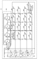
- FIG. 1 is a configuration diagram of a display panel driving apparatus according to the first embodiment.
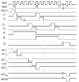
- FIG. 2 is a timing chart of the display panel driving device of FIG.
- FIG. 3 is another configuration diagram of the display panel driving device of FIG.
- FIG. 4 is another configuration diagram of the display panel driving device of FIG.
- FIG. 5 is another configuration diagram of the display panel driving device of FIG.
- FIG. 6 is a configuration diagram of a display panel driving apparatus according to the second embodiment.
- FIG. 7 is a configuration diagram of a display panel driving apparatus according to the third embodiment.
- FIG. 8 is a configuration diagram of a ring counter circuit according to the fourth embodiment.
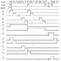
- FIG. 9 is a timing chart of the ring counter circuit of FIG.
- FIG. 1 is a configuration diagram of a display panel driving apparatus according to the first embodiment.
- the display panel driving device 10 outputs the scanning line driving signal OUT in order from the upper left to the lower right in the drawing.
- OUT is about 100 lines, and 1000 or more scanning lines are sequentially driven by connecting a plurality of display panel driving devices 10 in cascade.
- the SACT2 output from the display panel drive device 10 at the previous stage becomes the SACT1 of the display panel drive apparatus 10 at the next stage.
- the display panel driving device 10 can be configured by a ring counter circuit 100, a shift register 150, and a plurality of output units 200 that generate OUT.
- the ring counter circuit 100 includes, for example, one ring counter (first ring counter), and the ring counter can be configured by N stages of flip-flops 101_1 to 101_N connected in cascade.
- the flip-flops 101_1 to 101_N operate in synchronization with the clock signal CLK1 and output signals C 1 to C N , respectively.
- the signals C 1 to C N are output from the ring counter circuit 100 as they are.
- the first-stage flip-flop 101_1, and an output C N of the flip-flop 101_N scan line active signal SACT1 and final stage of the initial signal logic combined signal is input. Note that in the case where the first-stage flip-flop 101_1 has a set terminal, the flip-flop 101_1 may be directly set by the SACT1.
- the shift register 150 can be composed of M flip-flops 151_1 to 151_M connected in cascade.
- the flip-flops 151_1 to 151_M operate in synchronization with the clock signal CLK2, and output signals R 1 to R M , respectively.
- CLK2 is a signal having a frequency lower than that of CLK1, for example, a signal obtained by dividing CLK1 by N.
- the frequency dividing circuit 104 may divide CLK1 by N to generate CLK2 (see FIG. 3).
- the output of one of flip-flops for example, the output C 1 of the flip-flop 101_1 may be CLK2 (see FIG. 4).
- SACT1 is input to the first flip-flop 151_1.
- the output unit 200 can be composed of a logic circuit 201 and a level shifter 202.
- Logic circuit 201 is one of the outputs of the ring counter circuit 100, an output C 1 of the flip flop 101_1, which is one of the outputs of the shift register 0.99, NAND performing a logical operation of the output R 1 of the flip-flop 151_1 Can be configured.
- a through current prevention circuit may be connected between the logic circuit 201 and the level shifter 202.
- FIG. OUT 1 and OUT MN in FIG. 2 correspond to the upper left OUT and the lower right OUT in FIG. 1, respectively.
- the flip-flop 101_1 is set by SACT1, and C 1 to C N sequentially become H level in synchronization with CLK1.
- the flip-flop 151_1 is set by SACT1, and R 1 to R M sequentially become H level in synchronization with CLK2.
- C 1 to C N and R 1 to R M are logically operated, respectively, and OUT 1 to OUT MN sequentially become L level.
- N ⁇ M scanning line driving signals can be generated by N + M flip-flops.
- the ring counter in the ring counter circuit 100 may have one redundant flip-flop.
- N ⁇ M scanning line driving signals can be generated by (N + 1) + M flip-flops.
- the redundant number of flip-flops in the ring counter may be two or more.
- FIG. 6 is a configuration diagram of a display panel driving apparatus according to the second embodiment. Hereinafter, differences from the first embodiment will be described.
- the ring counter circuit 110 is a connection that switches between straight connection or reverse connection between the output terminals 111_1 to 111_N of the flip-flops 101_1 to 101_N and the output terminals 112_1 to 112_N of the ring counter circuit 110 according to the control signal FR.
- a switching unit 113 is included.
- the connection switching unit 113 can be composed of a plurality of selectors 113_1 to 113_N.
- the selector 113_1 selectively connects either the output end 111_1 or the output end 111_N to the output end 112_1 according to the FR.
- the selector 113_2 selectively connects either the output terminal 111_2 or the output terminal 111_N-1 to the output terminal 112_2 in accordance with the FR.
- the selector 113_N-1 selectively connects one of the output end 111_2 and the output end 111_N-1 to the output end 112_N-1 in accordance with the FR.
- the selector 113_N selectively connects either the output end 111_1 or the output end 111_N to the output end 112_N according to the FR.
- the shift register 160 is configured to be able to switch the first stage flip-flop to one of the flip-flops 161_1 and 161_M according to the FR.
- the shift register 160 is configured to be able to switch the shift direction according to the FR.
- the shift register 160 performs a forward shift with a signal input to each D1 terminal of the flip-flops 161_1 to 161_M.
- reverse shift is performed by signals input to the D2 terminals of the flip-flops 161_M to 161_1.
- the selector 120 selects either the output of the logic circuit 201 in the output unit 200 that outputs OUT first or the output of the logic circuit 201 in the output unit 200 that outputs OUT last in accordance with FR, and outputs it as SACT2. To do.
- the connection switching unit 113 connects the output terminals 111_1 to 111_N and the output terminals 112_1 to 112_N in a straight line.
- the selector 111_1 connects the output terminal 111_1 and the output terminal 112_1.
- the other selectors 113_2 to 113_N connect the output terminals 111_2 to 111_N and the output terminals 112_2 to 112_N, respectively.
- connection switching unit 113 reversely connects the output terminals 111_1 to 111_N and the output terminals 112_1 to 112_N.
- the selector 113_1 connects the output terminal 111_N and the output terminal 112_1.
- the other selectors 113_2 to 113_N connect the output terminals 111_N-1 to 111_1 and the output terminals 112_2 to 112_N, respectively.
- connection switching unit 113 of the ring counter circuit 110 may be omitted, and the flip-flops 101_1 and 101_N may be switched as the first-stage flip-flops and the shift direction may be switched according to the FR.
- a connection switching unit similar to the connection switching unit 113 may be provided in the shift register 160.
- the connection switching unit 113 of the ring counter circuit 110 is omitted, and the flip-flops 101_1 and 101_N are switched as the first-stage flip-flops and the shift direction is switched according to the FR, and the connection is switched to the shift register 160.
- a connection switching unit similar to the unit 113 may be provided.
- FIG. 7 is a configuration diagram of a display panel driving apparatus according to the third embodiment. Hereinafter, differences from the first embodiment will be described.
- the reset circuit 140 resets the ring counter, the shift register 150, and the frequency divider circuit 104 in the ring counter circuit 100, for example, at the timing when OUT is finally output from the display panel driving device 12. Further, the reset circuit 140 may adjust the timing by inserting a flip-flop or the like. Note that the reset circuit 140 may output a reset signal at the timing when any one of OUT is output, or may output the reset signal after receiving an external signal given at an arbitrary timing. Further, the reset circuit 140 may reset only the ring counter.
- the ring counter circuit may include two ring counters.
- the ring counter circuit is configured by two ring counters.
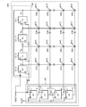
- FIG. 8 is a configuration diagram of a ring counter circuit according to the fourth embodiment.
- the ring counter circuit 120 can be composed of a first ring counter 130, a second ring counter 170, and a plurality of output units 210 that generate an output signal C.
- the first ring counter 130 can be composed of i-stage flip-flops 131_1 to 131_i connected in cascade.
- the flip-flops 131_1 to 131_i operate in synchronization with the clock signal CLK1, and output Q 1 to Q i , respectively.
- a signal obtained by logically synthesizing the scanning line active signal SACT1 as an initial signal and the output Q i of the final flip-flop 131_i is input to the first flip-flop 131_1. Note that in the case where the first-stage flip-flop 131_1 has a set terminal, the flip-flop 131_1 may be directly set by the SACT1.
- the second ring counter 170 can be composed of j-stage flip-flops 171_1 to 171_j connected in cascade.
- the flip-flops 171_1 to 171_j operate in synchronization with the clock signal CLK3, and output P 1 to P j , respectively.
- CLK3 is a signal having a frequency lower than that of CLK1, and is, for example, a signal obtained by dividing CLK1 by i. 3 may be provided to generate CLK3 by dividing CLK1 by i (see FIG. 3).
- the output Q 1 of the flip-flop 131_1 may be as CLK3. That is, the output of any one flip-flop in the first ring counter 130 can be CLK3.
- the first-stage flip-flop 171_1 the output P j of the flip-flop 171_j scan line active signal SACT1 and final stage of the initial signal logic combined signal is input. Note that in the case where the first-stage flip-flop 171_1 has a set terminal, the flip-flop 171_1 may be directly set by the SACT1.
- the output unit 210 may be configured to output P 1 of the output Q 1, flip-flop 171_1 of the flip-flop 131_1 an AND circuit for logical operations. That is, the ring counter circuit 120 performs a logical operation on the outputs Q 1 to Q i of the flip-flops 131_1 to 131_i and the outputs P 1 to P j of the flip-flops 171_1 to 171_j, and outputs the logical operation result as an output signal C. Output.
- the flip-flop 131_1 is set by SACT1, and Q 1 to Q i sequentially become H level in synchronization with CLK1. Further, the flip-flop 171_1 is set at SACT1, and P 1 to P j are sequentially set to the H level in synchronization with CLK3. Then, Q 1 to Q i and P 1 to P j are logically calculated, and C 1 to C ji are sequentially set to the H level.
- the ring counter in the ring counter circuit 100 may include redundant flip-flops. Therefore, in the present embodiment, the first ring counter 130 has 1 redundant flip-flop. You may have. In this case, since the total number of output units 210 does not change, one of the output units 210 arranged in the row direction in FIG. 8 may be omitted. As a result, the ring counter circuit 120 that outputs i ⁇ j signals by (i + 1) + j flip-flops can be configured. Note that the number of redundant flip-flops in the first ring counter 130 may be two or more.
- the ring counter circuit 120 of the present embodiment is applied to the ring counter circuit 110 shown in FIG. 6, the output order of the output C of the ring counter circuit 120 is reversed according to the control signal FR. That's fine.
- both the first and second ring counters 130 and 170 may be reset by the reset circuit 140.
- the ring counter circuit 120 is composed of the two ring counters 130 and 170.
- the ring counter circuit 120 is composed of three or more ring counters (for example, first to third ring counters). It's easy to do.
- the first to third ring counters operate in synchronization with clock signals having different frequencies.
- the output unit 210 may perform a logical operation on each output of the first to third ring counters. In this case, the result of the logical operation becomes one output of the ring counter circuit 120.
- the number of flip-flops used in the ring counter circuit is on the order of a power root of the number of outputs of the ring counter circuit.
- each component may operate with a signal having a logic opposite to that of the signal described above.
- the display panel driving device can reduce the circuit area, and thus is useful for television devices equipped with various flat panel displays.
Landscapes
- Engineering & Computer Science (AREA)
- Physics & Mathematics (AREA)
- Computer Hardware Design (AREA)
- General Physics & Mathematics (AREA)
- Theoretical Computer Science (AREA)
- Control Of Indicators Other Than Cathode Ray Tubes (AREA)
- Transforming Electric Information Into Light Information (AREA)
- Control Of El Displays (AREA)
- Liquid Crystal Display Device Control (AREA)
Abstract
Description
図1は、第1の実施形態に係る表示パネル駆動装置の構成図である。表示パネル駆動装置10は、図中の左上から右下の順に走査線駆動信号OUTを出力する。例えば、OUTは100本程度であり、表示パネル駆動装置10を複数個縦列接続することで1000本以上の走査線が順次駆動される。前段の表示パネル駆動装置10から出力されたSACT2は次段の表示パネル駆動装置10のSACT1となる。
図6は、第2の実施形態に係る表示パネル駆動装置の構成図である。以下、第1の実施形態との相違点を説明する。
図7は、第3の実施形態に係る表示パネル駆動装置の構成図である。以下、第1の実施形態との相違点を説明する。
図8は、第4の実施形態に係るリングカウンタ回路の構成図である。図8に示すように、リングカウンタ回路120は、第1のリングカウンタ130と、第2のリングカウンタ170と、出力信号Cを生成する複数の出力部210とで構成することができる。
100,110,120 リングカウンタ回路
130 第1のリングカウンタ
170 第2のリングカウンタ
104 分周回路
111_1~111_N 出力端
112_1~112_N 出力端
113 接続切替部
140 リセット回路
150,160 シフトレジスタ
200,210 出力部
Claims (10)
- 縦列接続された複数のフリップフロップを有し、初段のフリップフロップが初期信号でセットされ、第1のクロック信号に同期して動作する第1のリングカウンタを有し、前記複数のフリップフロップの出力を用いた信号を出力するリングカウンタ回路と、
縦列接続された複数のフリップフロップを有し、初段のフリップフロップが前記初期信号でセットされ、前記第1のクロック信号よりも低い周波数の第2のクロック信号に同期して動作するシフトレジスタと、
前記リングカウンタ回路のいずれか1つの出力と前記シフトレジスタのいずれか1つの出力とを論理演算して、表示パネルの走査線駆動信号を生成する出力部とを備えている
ことを特徴とする表示パネル駆動装置。 - 請求項1の表示パネル駆動装置において、
前記第1のクロック信号を分周して前記第2のクロック信号を生成する分周回路を備えている
ことを特徴とする表示パネル駆動装置。 - 請求項1の表示パネル駆動装置において、
前記第2のクロック信号は、前記第1のリングカウンタにおけるいずれか1つのフリップフロップの出力である
ことを特徴とする表示パネル駆動装置。 - 請求項1の表示パネル駆動装置において、
前記第1のリングカウンタおよび前記シフトレジスタはそれぞれ、共通の制御信号に応じて初段のフリップフロップおよびシフト方向が切り替え可能に構成されている
ことを特徴とする表示パネル駆動装置。 - 請求項1の表示パネル駆動装置において、
前記リングカウンタ回路は、制御信号に応じて、前記複数のフリップフロップの各出力端と当該リングカウンタ回路の各出力端とをストレート接続するかリバース接続するかを切り替える接続切替部を有するものであり、
前記シフトレジスタは、前記制御信号に応じて初段のフリップフロップおよびシフト方向が切り替え可能に構成されている
ことを特徴とする表示パネル駆動装置。 - 請求項1の表示パネル駆動装置において、
前記シフトレジスタは、制御信号に応じて、前記複数のフリップフロップの各出力端と当該シフトレジスタの各出力端とをストレート接続するかリバース接続するかを切り替える接続切替部を有するものであり、
前記第1のリングカウンタは、前記制御信号に応じて初段のフリップフロップおよびシフト方向が切り替え可能に構成されている
ことを特徴とする表示パネル駆動装置。 - 請求項1の表示パネル駆動装置において、
前記リングカウンタ回路は、制御信号に応じて、前記複数のフリップフロップの各出力端と当該リングカウンタ回路の各出力端とをストレート接続するかリバース接続するかを切り替える接続切替部を有するものであり、
前記シフトレジスタは、前記制御信号に応じて、前記複数のフリップフロップの各出力端と当該シフトレジスタの各出力端とをストレート接続するかリバース接続するかを切り替える接続切替部を有するものである
ことを特徴とする表示パネル駆動装置。 - 請求項1の表示パネル駆動装置において、
前記第1のリングカウンタをリセットするリセット回路を備えている
ことを特徴とする表示パネル駆動装置。 - 請求項1乃至8のうちいずれか1つの表示パネル駆動装置において、
前記リングカウンタ回路は、
縦列接続された複数のフリップフロップを有し、初段のフリップフロップが前記初期信号でセットされ、前記第1のクロック信号よりも低い周波数の第3のクロック信号に同期して動作する第2のリングカウンタと、
前記第1のリングカウンタのいずれか1つの出力と、前記第2のリングカウンタのいずれか1つの出力とを論理演算して、当該リングカウンタ回路の出力を生成する出力部とを有している
ことを特徴とする表示パネル駆動装置。 - 請求項1乃至8のうちいずれか1つの表示パネル駆動装置において、
前記リングカウンタ回路は、それぞれ異なる周波数のクロック信号に同期して動作する、前記第1のリングカウンタを含む、複数のリングカウンタを有するものであり、前記複数のリングカウンタのそれぞれのいずれか1つの出力を論理演算し、その論理演算結果を、当該リングカウンタ回路のいずれか1つの出力とする
ことを特徴とする表示パネル駆動装置。
Priority Applications (3)
| Application Number | Priority Date | Filing Date | Title |
|---|---|---|---|
| JP2012526277A JPWO2012014361A1 (ja) | 2010-07-30 | 2011-06-06 | 表示パネル駆動装置 |
| CN2011900006296U CN203118406U (zh) | 2010-07-30 | 2011-06-06 | 显示面板驱动装置 |
| US13/733,836 US8594270B2 (en) | 2010-07-30 | 2013-01-03 | Display panel drive device |
Applications Claiming Priority (2)
| Application Number | Priority Date | Filing Date | Title |
|---|---|---|---|
| JP2010-171686 | 2010-07-30 | ||
| JP2010171686 | 2010-07-30 |
Related Child Applications (1)
| Application Number | Title | Priority Date | Filing Date |
|---|---|---|---|
| US13/733,836 Continuation US8594270B2 (en) | 2010-07-30 | 2013-01-03 | Display panel drive device |
Publications (1)
| Publication Number | Publication Date |
|---|---|
| WO2012014361A1 true WO2012014361A1 (ja) | 2012-02-02 |
Family
ID=45529600
Family Applications (1)
| Application Number | Title | Priority Date | Filing Date |
|---|---|---|---|
| PCT/JP2011/003180 Ceased WO2012014361A1 (ja) | 2010-07-30 | 2011-06-06 | 表示パネル駆動装置 |
Country Status (4)
| Country | Link |
|---|---|
| US (1) | US8594270B2 (ja) |
| JP (1) | JPWO2012014361A1 (ja) |
| CN (1) | CN203118406U (ja) |
| WO (1) | WO2012014361A1 (ja) |
Cited By (1)
| Publication number | Priority date | Publication date | Assignee | Title |
|---|---|---|---|---|
| CN114203124A (zh) * | 2021-11-30 | 2022-03-18 | 重庆惠科金渝光电科技有限公司 | 栅极驱动方法、栅极驱动电路及显示器 |
Families Citing this family (2)
| Publication number | Priority date | Publication date | Assignee | Title |
|---|---|---|---|---|
| US11955059B2 (en) | 2021-03-26 | 2024-04-09 | Forth Dimension Display, Ltd | Apparatuses, systems, and methods for MicroLED (mLED) backplane architectures |
| CN119360761A (zh) * | 2023-07-24 | 2025-01-24 | 武汉华星光电半导体显示技术有限公司 | 栅极驱动单元及显示装置 |
Citations (5)
| Publication number | Priority date | Publication date | Assignee | Title |
|---|---|---|---|---|
| JPH05313129A (ja) * | 1992-05-07 | 1993-11-26 | Fujitsu Ltd | 液晶表示装置 |
| JPH09243993A (ja) * | 1996-03-06 | 1997-09-19 | Seiko Epson Corp | 液晶装置および電子機器 |
| JPH11296129A (ja) * | 1998-04-07 | 1999-10-29 | Sony Corp | 画素駆動回路および駆動回路一体型画素集積装置 |
| JPH11338429A (ja) * | 1998-05-25 | 1999-12-10 | Sharp Corp | 液晶表示装置及びその駆動方法 |
| JP2005070673A (ja) * | 2003-08-27 | 2005-03-17 | Renesas Technology Corp | 半導体回路 |
Family Cites Families (8)
| Publication number | Priority date | Publication date | Assignee | Title |
|---|---|---|---|---|
| US4180813A (en) * | 1977-07-26 | 1979-12-25 | Hitachi, Ltd. | Liquid crystal display device using signal converter of digital type |
| US4742346A (en) * | 1986-12-19 | 1988-05-03 | Rca Corporation | System for applying grey scale codes to the pixels of a display device |
| US5101203A (en) * | 1990-06-29 | 1992-03-31 | International Business Machines Corporation | Digital data regeneration and deserialization circuits |
| US6437766B1 (en) | 1998-03-30 | 2002-08-20 | Sharp Kabushiki Kaisha | LCD driving circuitry with reduced number of control signals |
| JP2002132203A (ja) | 2000-10-25 | 2002-05-09 | Matsushita Electric Ind Co Ltd | パネル駆動用半導体回路装置 |
| JP4076963B2 (ja) * | 2004-02-06 | 2008-04-16 | シャープ株式会社 | シフトレジスタ及び表示装置 |
| JP4546311B2 (ja) * | 2005-03-31 | 2010-09-15 | Nec液晶テクノロジー株式会社 | アクティブマトリクス型双安定性表示装置 |
| WO2007083410A1 (ja) * | 2006-01-23 | 2007-07-26 | Sharp Kabushiki Kaisha | 駆動回路およびそれを備えた表示装置ならびに表示装置の駆動方法 |
-
2011
- 2011-06-06 WO PCT/JP2011/003180 patent/WO2012014361A1/ja not_active Ceased
- 2011-06-06 JP JP2012526277A patent/JPWO2012014361A1/ja not_active Withdrawn
- 2011-06-06 CN CN2011900006296U patent/CN203118406U/zh not_active Expired - Fee Related
-
2013
- 2013-01-03 US US13/733,836 patent/US8594270B2/en not_active Expired - Fee Related
Patent Citations (5)
| Publication number | Priority date | Publication date | Assignee | Title |
|---|---|---|---|---|
| JPH05313129A (ja) * | 1992-05-07 | 1993-11-26 | Fujitsu Ltd | 液晶表示装置 |
| JPH09243993A (ja) * | 1996-03-06 | 1997-09-19 | Seiko Epson Corp | 液晶装置および電子機器 |
| JPH11296129A (ja) * | 1998-04-07 | 1999-10-29 | Sony Corp | 画素駆動回路および駆動回路一体型画素集積装置 |
| JPH11338429A (ja) * | 1998-05-25 | 1999-12-10 | Sharp Corp | 液晶表示装置及びその駆動方法 |
| JP2005070673A (ja) * | 2003-08-27 | 2005-03-17 | Renesas Technology Corp | 半導体回路 |
Cited By (1)
| Publication number | Priority date | Publication date | Assignee | Title |
|---|---|---|---|---|
| CN114203124A (zh) * | 2021-11-30 | 2022-03-18 | 重庆惠科金渝光电科技有限公司 | 栅极驱动方法、栅极驱动电路及显示器 |
Also Published As
| Publication number | Publication date |
|---|---|
| JPWO2012014361A1 (ja) | 2013-09-09 |
| US20130114782A1 (en) | 2013-05-09 |
| US8594270B2 (en) | 2013-11-26 |
| CN203118406U (zh) | 2013-08-07 |
Similar Documents
| Publication | Publication Date | Title |
|---|---|---|
| US9542878B2 (en) | Shift register unit, display panel and display apparatus | |
| US10134353B2 (en) | Gate driving circuit, display panel and display apparatus having the same, and driving method thereof | |
| CN104700806B (zh) | 一种移位寄存器、栅极驱动电路、显示面板及显示装置 | |
| US20110316821A1 (en) | Driving circuit, liquid crystal display apparatus and electronic information device | |
| US10152164B2 (en) | Touch driving circuit, touch driving method and touch screen | |
| US20190057638A1 (en) | Shift-buffer circuit, gate driving circuit, display panel and driving method | |
| JP2020520038A (ja) | シフトレジスタユニット及びその制御方法、ゲート駆動回路、表示装置 | |
| EP3236459A1 (en) | Scanning drive circuit and display device | |
| CN110738953B (zh) | 栅极驱动器及具有栅极驱动器的显示装置 | |
| CN105047120B (zh) | 一种栅极驱动电路及其驱动方法、显示装置 | |
| US9519372B2 (en) | Gate driving circuit for time division driving, method thereof and display apparatus having the same | |
| CN108665845B (zh) | 显示面板和显示装置 | |
| US9135870B2 (en) | Source driver, controller, and method for driving source driver | |
| WO2012014361A1 (ja) | 表示パネル駆動装置 | |
| US6765980B2 (en) | Shift register | |
| CN106991955A (zh) | 扫描驱动电路、显示面板以及驱动方法 | |
| CN107016954A (zh) | 一种显示面板 | |
| JP5027435B2 (ja) | 半導体集積回路装置 | |
| WO2021103140A1 (zh) | 驱动电路 | |
| US7948466B2 (en) | Circuit structure for dual resolution design | |
| CN205177380U (zh) | 一种移位寄存单元、触控显示面板及触控显示装置 | |
| TW201705117A (zh) | 顯示器及其驅動方法 | |
| US7683878B2 (en) | Systems for providing dual resolution control of display panels | |
| CN100547649C (zh) | 显示面板双分辨率控制系统 | |
| CN108109598A (zh) | 一种goa电路及液晶显示面板 |
Legal Events
| Date | Code | Title | Description |
|---|---|---|---|
| WWE | Wipo information: entry into national phase |
Ref document number: 201190000629.6 Country of ref document: CN |
|
| 121 | Ep: the epo has been informed by wipo that ep was designated in this application |
Ref document number: 11811968 Country of ref document: EP Kind code of ref document: A1 |
|
| WWE | Wipo information: entry into national phase |
Ref document number: 2012526277 Country of ref document: JP |
|
| NENP | Non-entry into the national phase |
Ref country code: DE |
|
| 122 | Ep: pct application non-entry in european phase |
Ref document number: 11811968 Country of ref document: EP Kind code of ref document: A1 |