WO2012014351A1 - 固体撮像装置 - Google Patents
固体撮像装置 Download PDFInfo
- Publication number
- WO2012014351A1 WO2012014351A1 PCT/JP2011/002020 JP2011002020W WO2012014351A1 WO 2012014351 A1 WO2012014351 A1 WO 2012014351A1 JP 2011002020 W JP2011002020 W JP 2011002020W WO 2012014351 A1 WO2012014351 A1 WO 2012014351A1
- Authority
- WO
- WIPO (PCT)
- Prior art keywords
- wiring
- potential
- imaging device
- solid
- state imaging
- Prior art date
- Legal status (The legal status is an assumption and is not a legal conclusion. Google has not performed a legal analysis and makes no representation as to the accuracy of the status listed.)
- Ceased
Links
Images





Classifications
-
- H—ELECTRICITY
- H10—SEMICONDUCTOR DEVICES; ELECTRIC SOLID-STATE DEVICES NOT OTHERWISE PROVIDED FOR
- H10F—INORGANIC SEMICONDUCTOR DEVICES SENSITIVE TO INFRARED RADIATION, LIGHT, ELECTROMAGNETIC RADIATION OF SHORTER WAVELENGTH OR CORPUSCULAR RADIATION
- H10F39/00—Integrated devices, or assemblies of multiple devices, comprising at least one element covered by group H10F30/00, e.g. radiation detectors comprising photodiode arrays
- H10F39/80—Constructional details of image sensors
- H10F39/802—Geometry or disposition of elements in pixels, e.g. address-lines or gate electrodes
-
- H—ELECTRICITY
- H04—ELECTRIC COMMUNICATION TECHNIQUE
- H04N—PICTORIAL COMMUNICATION, e.g. TELEVISION
- H04N25/00—Circuitry of solid-state image sensors [SSIS]; Control thereof
- H04N25/50—Control of the SSIS exposure
- H04N25/57—Control of the dynamic range
- H04N25/59—Control of the dynamic range by controlling the amount of charge storable in the pixel, e.g. modification of the charge conversion ratio of the floating node capacitance
-
- H—ELECTRICITY
- H04—ELECTRIC COMMUNICATION TECHNIQUE
- H04N—PICTORIAL COMMUNICATION, e.g. TELEVISION
- H04N25/00—Circuitry of solid-state image sensors [SSIS]; Control thereof
- H04N25/70—SSIS architectures; Circuits associated therewith
- H04N25/76—Addressed sensors, e.g. MOS or CMOS sensors
- H04N25/767—Horizontal readout lines, multiplexers or registers
-
- H—ELECTRICITY
- H10—SEMICONDUCTOR DEVICES; ELECTRIC SOLID-STATE DEVICES NOT OTHERWISE PROVIDED FOR
- H10F—INORGANIC SEMICONDUCTOR DEVICES SENSITIVE TO INFRARED RADIATION, LIGHT, ELECTROMAGNETIC RADIATION OF SHORTER WAVELENGTH OR CORPUSCULAR RADIATION
- H10F39/00—Integrated devices, or assemblies of multiple devices, comprising at least one element covered by group H10F30/00, e.g. radiation detectors comprising photodiode arrays
- H10F39/10—Integrated devices
- H10F39/12—Image sensors
- H10F39/18—Complementary metal-oxide-semiconductor [CMOS] image sensors; Photodiode array image sensors
Definitions
- the present invention relates to a solid-state imaging device, and more particularly to a MOS solid-state imaging device.
- Solid-state imaging devices used as imaging devices such as digital still cameras and surveillance cameras are roughly classified into two types: CCD (Charge Coupled Device) type solid-state imaging devices and MOS (Metal Oxide Semiconductor) type solid-state imaging devices.
- CCD Charge Coupled Device
- MOS Metal Oxide Semiconductor
- MOS type solid-state imaging devices are expanding their applications such as digital still cameras and surveillance cameras because of their high speed and low power consumption. In these fields, finer images are demanded, and in order to realize them, it is necessary to increase the number of pixels of the solid-state imaging device.
- each pixel cell in the solid-state imaging device receives light, generates and accumulates photocharges, a transfer transistor 902 that transfers photocharges from the photodiodes 901, and a transfer transistor 902.
- a floating diffusion 903 to which photo charges are transferred a storage capacitor element 908 that stores photo charges overflowing from the photodiode 901 during the storage operation, a storage transistor 907 that couples or divides the potential of the floating diffusion 903 and the storage capacitor element 908, and a floating diffusion 903
- the reset transistor 906 for discharging the photoelectric charge in the floating diffusion 903 and the photoelectric charge in the floating diffusion 903 are connected to the voltage signal.
- Amplifying transistor 904 that amplifies converted to (pixel signal), and is formed by connecting the amplifier transistor 904, and a selection transistor 905 for selecting a pixel cell.
- the operation of the solid-state imaging device shown in FIG. 12 is executed as follows.
- the potential change ⁇ V is amplified by the amplification transistor 904, and is output through the signal line 95 when the selection transistor 905 is turned on by applying the selection control signal Xx.
- the solid-state imaging device according to the above-described prior art needs to have a configuration in which the storage capacitor element 908 and the storage transistor 907 are added to each pixel cell, the area of the photodiode 901 has to be reduced accordingly. Absent. For this reason, the solid-state imaging device according to the related art has a problem that the amount of charge that can be generated and accumulated by the photodiode 901 is reduced, and the dynamic range is deteriorated.
- the present invention has been made to solve such a problem, and provides a solid-state imaging device capable of suppressing a reduction in the area of a photodiode and achieving both a high S / N ratio and a high dynamic range.
- the purpose is to provide.
- the solid-state imaging device according to the present invention adopts the following configuration.
- the solid-state imaging device is a device that has a plurality of two-dimensionally arranged pixel cells and outputs pixel signals generated by the plurality of pixel cells.
- Each of the plurality of pixel cells includes one or more photodiodes, a transfer transistor, a reset transistor, and an amplification transistor.
- the photodiode generates a signal charge by photoelectric conversion.
- the transfer transistor is provided corresponding to the photodiode, and transfers the signal charge generated by the photodiode to the charge conversion unit in accordance with the transfer control signal.
- the reset transistor controls the potential state of the charge conversion unit according to the reset control signal.
- the amplification transistor amplifies and converts the signal charge into a pixel signal according to the signal charge transferred to the charge conversion unit, and outputs it to the signal line.
- a wiring for forming a parasitic capacitance with each charge conversion unit is attached to at least a part of the plurality of pixel cells.
- a switching portion that selectively switches the potential state of the wiring between a fixed potential and a potential that follows the potential of the signal line is connected.
- wiring is attached to at least some pixel cells, and a switching unit is connected to the wiring. For this reason, in the pixel cell provided with the wiring, a parasitic capacitance is formed between the charge conversion portion (floating diffusion) and the wiring. Since the potential state of the wiring can be selectively switched between a fixed potential and a potential following the potential of the signal line by switching the switching unit, the charge conversion unit and the wiring can be switched by switching the potential. The parasitic capacitance between and changes.
- the switching unit can be switched to a fixed potential, the parasitic capacitance of the charge conversion unit can be increased to reduce the potential change of the charge conversion unit, and a high dynamic range can be realized. it can.
- the switching unit is switched to a potential that follows the potential of the signal line, the parasitic capacitance of the charge conversion unit is reduced, and the potential change of the charge conversion unit is increased.
- An S / N ratio can be realized.
- the solid-state imaging device in order to achieve both a high S / N ratio and a high dynamic range, only the wiring is attached to the pixel cell. Compared with the solid-state imaging device, the area of the photodiode can be maintained larger by the amount of the transistor and the capacitor. Therefore, the solid-state imaging device according to the present invention can achieve a high dynamic range.
- the gain can be changed by the charge conversion unit (floating diffusion) closer to the signal source, the influence of noise can be reduced and a high S / N ratio can be realized.
- the solid-state imaging device it is possible to suppress a reduction in the area of the photodiode and achieve both a high S / N ratio and a high dynamic range.
- FIG. 1 is a schematic block diagram showing an overall configuration of a solid-state imaging device 1 according to Embodiment 1.
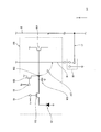
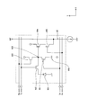
- FIG. 2 is a schematic circuit diagram showing a configuration of a pixel cell 100 and its peripheral configuration in the solid-state imaging device 1;
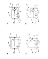
- FIG. 6 is a potential diagram when signal charges are output in the solid-state imaging device 1, where (a) and (b) show the case where the wiring 16 is set to a fixed potential (ground), and (c) and (d) are A case where the wiring 16 is connected to the signal line 15 is shown.
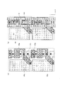
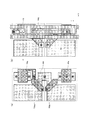
- (A), (b) is a schematic top view which shows the layout of the pixel cell 100 and the wiring 16 in the solid-state imaging device 1 in order of lamination
- (A), (b) is a schematic top view which shows the layout of the pixel cell 100 and the wiring 16 in the solid-state imaging device 1 in order of lamination
- (A), (b) is a schematic top view which shows the layout of the pixel cell and wiring in the solid-state imaging device concerning Embodiment 2 in order of lamination.
- (A), (b) is a schematic plan view which shows the layout of the pixel cell and wiring in the solid-state imaging device concerning Embodiment 2 in order of lamination
- 6 is a schematic circuit diagram showing a partial configuration of a solid-state imaging device 3 according to Embodiment 3.
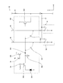
- FIG. 6D is a schematic circuit diagram illustrating a switching unit 43 according to Modification 4; 6 is a schematic circuit diagram showing a partial configuration of a solid-state imaging device 5 according to Embodiment 4.
- FIG. (A), (b) is a schematic top view which shows the layout of the pixel cell in the solid-state imaging device concerning Embodiment 5 in order of lamination
- a plurality of pixel cells 100 are arranged in a matrix (matrix), and a pixel array 10 is configured therefrom.
- a vertical shift register 11, a horizontal shift register 12, and a pulse generation circuit 13 are connected to the pixel array 10.
- a switching unit 14 is connected to the pixel array 10 for each column.
- the vertical shift register 11 and the horizontal shift register 12 are both dynamic circuit units, for example, and sequentially output drive pulses to each pixel cell 10 in response to the application of timing pulses from the pulse generation circuit 13. To do.
- Each pixel cell 100 outputs a pixel signal in accordance with the drive pulse.
- the pixel cell 100 includes one photodiode 101 and three transistors 102, 104, and 105. One end of the photodiode 101 is grounded, and the other end is connected to the source of the transfer transistor 102.
- the drain of the transfer transistor 102 is connected to the gate of the amplification transistor 104 and the source of the reset transistor 105 via the floating diffusion (charge conversion unit) 103.
- the drain of the amplification transistor 104 is connected to the power supply voltage VDD, and the source is connected to the signal line 15.
- the photodiode 101 is an element unit having a photoelectric conversion function for generating a signal charge according to the intensity of light incident on each pixel cell 100.
- the transfer transistor 102 is an element unit for transferring signal charges from the photodiode 101 to the floating diffusion 103 in accordance with a transfer control signal Tx to the gate.
- the amplification transistor 104 is an element unit that outputs the signal charge transferred to the floating diffusion 103 to the signal line 15.
- the reset transistor 105 is an element unit that resets the signal charge accumulated in the drain of the transfer transistor 102 and the floating diffusion 103 in accordance with the reset control signal Rx to the gate.
- the amplification transistor 104 has a function of performing amplification conversion into a pixel signal corresponding to the signal charge, and the remaining transfer transistor 102 and reset transistor 105 have a switching function. is there.
- the pixel cell 100 is provided with a wiring 16 extending in the Y-axis direction.
- a switching unit 14 is connected to one end of the wiring 16.
- One terminal of the switching unit 14 is connected to the signal line 15 via the connection wiring 17.
- the potential state of the wiring 16 can be selectively switched to a potential following the ground potential and the potential of the signal line 15 by the switching unit 14. Note that the switching unit 14 is arranged outside the pixel array 10 (see FIG. 1).
- a parasitic capacitance 107 is formed between the wiring 16 and the wiring.
- the switching unit 14 selectively switches the connection destination of the wiring 16 between the ground and the signal line 15 according to the amount of charge Q accumulated in the photodiode 101, thereby the potential state of the wiring 16. Can be selectively switched between the ground potential and the potential following the potential of the signal line 15. Therefore, the gain can be selectively changed, and a large output can be obtained.
- a wiring 16 is attached to the pixel cell 100, and the switching unit 14 is connected to the wiring 16.
- a parasitic capacitance 107 (capacitance Cgs) is formed between the floating diffusion 103 and the wiring 16.
- the potential state of the wiring 16 can be selectively switched between a fixed potential (ground potential) and a potential that follows the potential of the signal line 15 by switching the switching unit 14.
- the value Cgs of the parasitic capacitance 107 between the floating diffusion 103 and the wiring 16 changes.
- two types of potential states can be obtained in the floating diffusion 103 by selectively switching the switching unit 14. For example, when the charge Q accumulated in the photodiode 101 is large, the switching unit 14 is switched to the ground potential, and the parasitic capacitance of the floating diffusion 103 is increased (parasitic capacitance 106 (capacitance Cfd) and parasitic capacitance 107 (capacitance Cgs). )), The potential change ⁇ V of the floating diffusion 103 can be reduced, and a high dynamic range can be realized.
- the switching unit 14 is switched to a potential that follows the potential of the signal line 15, and the parasitic capacitance of the charge conversion unit is reduced to make a floating diffusion (charge conversion unit).
- the potential change at 103 can be increased and a high S / N ratio can be realized.
- the solid-state imaging device 1 only the wiring 16 is attached to the pixel cell 100 in order to achieve both a high S / N ratio and a high dynamic range as described above. Compared with the imaging device, the area of the photodiode can be maintained larger by the amount of the transistor and the capacitor. Therefore, in the solid-state imaging device 1 according to the present embodiment, a high dynamic range can be realized.
- the gain can be changed by the floating diffusion 103 closer to the signal source, the influence of noise can be reduced and a high S / N ratio can be realized.
- the solid-state imaging device 1 according to the present embodiment, a reduction in the area of the photodiode 101 can be suppressed, and both a high S / N ratio and a high dynamic range can be achieved.
- the gate 102g of the transfer transistor 102 is provided on the lower left side in the XY direction with respect to the photodiode 101 provided for each pixel cell 100.
- the drain of the transfer transistor 102 is a diffusion layer portion 1031 that is an element of the floating diffusion 103.
- the diffusion layer portion 1031 of the floating diffusion 103 is connected to the gate 104g of the amplification transistor 104 via the wiring portion 1032 of the floating diffusion 103 shown in FIG. 4B (see FIG. 4A).
- the gate 105g of the reset transistor 105 is provided on the lower side in the Y-axis direction with respect to the diffusion layer portion 1031 of the floating diffusion 103.
- the drain of the amplification transistor 104 is connected to the power supply line VDD-L, and the source is connected to the wiring portion 151 of the signal line 15.
- the wiring 16 is provided in parallel with the wiring portion 1032 of the floating diffusion 103.
- the wiring 16 is extended in the Y-axis direction.
- each pixel cell 100 is provided with control lines 18 and 19 extending in the X-axis direction.
- the control line 18 is connected to the gate 102g of the transfer transistor 102, and the control line 19 is connected to the gate 105g of the reset transistor 105.
- the wiring part 152 is formed so as to cover a part of the wiring part 151 and the wiring part 1032 of the floating diffusion 103 and is connected to the wiring part 151.
- a wiring part 153 formed on the upper layer and covering the part of the wiring part 152 and connected to the wiring part 152 is provided.
- the wiring part 153 extends in the Y-axis direction.
- the wiring portion 1032 and the wiring 16 of the floating diffusion 103 can be run in parallel (see FIG. 4B), and between the floating diffusion 103 and the wiring 16 can be obtained.
- the parasitic capacitance 107 (capacitance Cgc) can be increased, and as described above, a high S / N ratio and a high dynamic range can be realized.
- the wiring width is 100 [nm]
- the wiring interval is 100 [nm]
- the wiring interval in the stacking direction is 100 [nm].
- the thickness (thickness) is 200 [nm].
- FIGS. 4 and 5 a layout as shown in FIGS. 4 and 5 is adopted.
- FIGS. 6 and 7 are layout diagrams for each layer showing the layout of pixel cells and wirings, and correspond to FIGS. 4 and 5 used in the first embodiment.
- a transfer transistor gate 202g is provided on the lower left side in the XY direction with respect to the photodiode 201 provided for each pixel cell.
- the drain of the transfer transistor is a diffusion layer portion 2031 that is an element of floating diffusion.
- the diffusion layer portion 2031 of the floating diffusion is connected to the gate 204g of the amplification transistor via the wiring portion 2032 of the floating diffusion shown in FIG. 6B (see FIG. 6A).
- a reset transistor gate 205g is provided on the lower side in the Y-axis direction with respect to the diffusion layer 2031 of the floating diffusion.
- the source of the amplification transistor is connected to the signal line 25.
- the wiring part 261 of the wiring is provided in parallel with the wiring part 2032 connected to the diffusion layer part 2031 of the floating diffusion.
- the wiring part 261 of the wiring is extended in the Y-axis direction.
- each pixel cell is provided with control lines 28 and 29 extending in the X-axis direction, as in the first embodiment.
- the control line 28 is connected to the gate 202g of the transfer transistor, and the control line 29 is connected to the gate 205g of the reset transistor.
- a wiring part 262 connected to the wiring part 261 is provided on the wiring part 2032 of the floating diffusion.
- the wiring portion 262 covers the floating diffusion wiring portion 2032 and is in a relationship facing the same.
- a power supply line VDD-L extending in the Y-axis direction is formed on the wiring portion 2032 of the floating diffusion.
- the power supply line VDD-L is connected to the drain of the amplification transistor 104.
- the wiring portion 262 of the wiring is also provided on the wiring portion 2032 of the floating diffusion as compared with the solid-state imaging device 1 according to the first embodiment. Is provided.
- the parasitic capacitance Cgs between the floating diffusion and the wiring can be further increased, so that both a high S / N ratio and a high dynamic range can be achieved. It is effective.
- the wiring layer 261 of the wiring is also disposed on the gate of the amplification transistor, it is possible to further increase the parasitic capacitance Cgs (see FIG. 6 (b)). Further, since the wiring portion 261 of the wiring is also disposed on the diffusion layer portion 2031 of the floating diffusion, the parasitic capacitance Cgs can be further increased, and both a high S / N ratio and a high dynamic range are achieved. It is effective.
- the layout in which the wiring portion 2032 of the floating diffusion is the first layer and the wiring portion 262 of the wiring is the second layer is used as an example.
- the capacity Cgs can be increased, and both a high S / N ratio and a high dynamic range can be achieved.
- Embodiment 3 The configuration of the solid-state imaging device 3 according to Embodiment 3 will be described with reference to FIG.
- a plurality of pixel cells 300 are provided in a matrix to form a pixel array 30.
- the pixel array 30 is provided with signal lines 35 1 to 35 n and wirings 36 1 to 36 n for each column.
- the wiring 36 1 ⁇ 36 n are outside the pixel array 30, the switching unit 34u 1 ⁇ 34u n, it is 34l 1 ⁇ 34l n are connected to the Y-axis direction and low extremes.
- Switching unit 34u 1 ⁇ 34u n are connected to the connection line 37u 1 ⁇ 37u n having one end connected to the signal lines 35 1 ⁇ 35 n.
- Switching unit 34l 1 ⁇ 34l n are connected to the connection line 37l 1 ⁇ 37l n having one end connected to the signal lines 35 1 ⁇ 35 n.
- the solid-state imaging device 3 in each outer upper and lower Y-axis direction with respect to the pixel array 30, and the switching unit 34u 1 ⁇ 34u n, it is 34l 1 ⁇ 34l n provided, thereby the signal line
- the opening / closing operation for 35 1 to 35 n can be executed. Therefore, in the solid-state imaging device 3 according to the present embodiment, the potential states of the wirings 36 1 to 36 n are selectively compared with the solid-state imaging device 1 according to the first embodiment while minimizing the time delay. You can switch to
- Modification 1 A modification example of the switching unit that selectively switches the wiring state between a fixed potential and a potential that follows the potential of the signal line will be described with reference to FIG.
- the switching unit 41 according to the modification 1 is inserted between the nMOS element 411 interposed between the wiring 46 and the ground, and between the wiring 46 and the connection line 47.
- the connection line 47 is connected to the signal line 45.
- control signal Gx is “L level”
- the pMOS element 412 between the wiring 46 and the connection line 47 is turned on, and the wiring 46 has a potential that follows the potential of the signal line 45.
- the switching unit 41 can be configured with a minimum element configuration.
- the switching unit 42 according to the present modification is similar to the switching unit 41 according to the first modification, in addition to the nMOS element unit 421 and the pMOS element unit 422, and the control signal Gx
- An inverter 423 connected to the signal line, and an nMOS element portion 424 inserted between the wiring 46 and the connection line 47 are added.
- the potential of the signal line 45 when the potential of the signal line 45 is lowered, the potential may not be the same before and after the nMOS element 424 in the signal line 45.
- the switching unit 42 since the nMOS element 424 is connected in parallel to the pMOS element 422, even when the potential of the signal line 45 decreases, the nMOS in the signal line 45 There is a possibility that the potential is not the same before and after the element 424, but this can be eliminated.
- the switching unit 43 according to the present modification is similar to the switching unit 42 according to the second modification in that the nMOS element 431 and the inverter 433 are included.
- a difference is that source followers of nMOS elements 432 and 434 are provided instead of the pMOS element 422 and the nMOS element 424 connected in parallel in the second modification.
- the wiring 46 is driven by the source follower configured by the nMOS elements 432 and 434, so that the operation speed can be improved.
- the switching unit 44 according to the present modification is similar to the switching unit 43 according to the third modification, except that the nMOS elements 441 and 444 and the inverter 443 are included. Then, it is different in that an operational amplifier 442 is provided instead of the nMOS element 432 constituting the source follower in the switching unit 43 according to the third modification.
- the switching unit 44 according to the present modification it is possible to improve the operation speed in the same manner as the switching unit 43 according to the third modification. At this time, if the gain of the operational amplifier 442 is selectively changed, the amount of change in potential of the wiring 46 following the potential of the signal line 45 can be varied. Therefore, the switching unit 44 according to the present modification can realize several types of conversion efficiency in the floating diffusion.
- the switching unit 44 according to the present modification is employed, the conversion efficiency in the floating diffusion with the customized charge Q can be selected, and the operation with a higher S / N ratio becomes possible.
- the ground potential is applied as an example of the fixed potential.
- a potential used for driving a pixel cell such as a power supply potential of an amplification transistor or a reset transistor can be applied. Since these potential wirings are arranged around the pixel arrays 10 and 30, there is no problem of occupation of the area for this purpose.
- the nMOS element 411 can be changed to a pMOS element, and there is no need for well separation. A simple configuration can be obtained.
- each pixel cell 500 includes a photodiode 501, a transfer transistor 502, an amplification transistor 504, and a reset transistor 505.
- the drain of the transfer transistor 502 is a floating diffusion 503.
- the drain of the amplification transistor 504 is connected to the power supply voltage VDD, and the source is connected to the signal line 55.
- the gate of the transfer transistor 502 is connected to the control line 58 and receives an input of the transfer control signal Tx.
- the gate of the reset transistor 505 is connected to the control line 59 and receives the input of the reset control signal Rx.
- two wirings 56 and 60 are attached to the pixel cell 500.
- the switching portions 54 and 61 are connected to the two wirings 56 and 60 at one end, respectively.
- Each of the switching units 54 and 61 can selectively switch between grounding and the connection line 57.
- the connection line 57 is connected to the signal line 55.
- a parasitic capacitance 506 between the parasitic capacitance 506 and the wiring 56 and a parasitic capacitance 508 between the wiring 60 are formed in the floating diffusion 503. .
- the potential change in the floating diffusion 503 is as follows.
- the two wirings 56 and 60 are attached to the pixel cell 500.
- the number of attached wirings and the selection destination as a fixed potential are limited to this. Not receive.
- three or more wirings may be attached to the pixel cell 500, and the configuration of the third embodiment shown in FIG. 8 may be used in combination.
- Embodiment 5 The configuration of the solid-state imaging device according to Embodiment 5 will be described with reference to FIG.
- the solid-state imaging device includes two photodiodes 701u and 701l in one pixel cell.
- a transfer transistor is connected to each of the photodiodes 701u and 701l, and gates 702ug and 702lg of the transfer transistor are provided correspondingly.
- the drain of the transfer transistor is connected to the diffusion layer portion 7031 of the floating diffusion.
- one amplification transistor and one reset transistor are provided for each of the two photodiodes 701u and 701l.
- an amplification transistor gate 704g is provided on the upper side in the Y-axis direction with respect to the diffusion layer portion 7031 of the floating diffusion, and a reset transistor gate 705g is provided on the lower side.
- a floating diffusion wiring portion 7032 connected to the floating diffusion diffusion portion 7031 is provided above the floating diffusion diffusion layer portion 7031.
- the floating diffusion wiring part 7032 extends in the Y-axis direction.
- a signal line 75 is connected to the source of the amplification transistor.
- the wiring 76 is provided in a state of running parallel to the wiring portion 7032 of the floating diffusion.
- the wiring 76 extends in the Y-axis direction and is connected to the switching unit outside the pixel array (not shown).
- the wiring 76 is provided in a state of running parallel to the wiring portion 7032 of the floating diffusion, and the potential state of the wiring 76 is caused by the switching operation of the switching unit not shown. Can be selectively switched between a fixed potential and a potential following the potential of the signal line 75, so that a high S / N ratio and a high dynamic range can be obtained as described above. .
- a solid-state imaging device having a so-called two-pixel one-cell configuration is taken as an example.
- the present invention is not limited thereto, and the solid-state imaging device having a multi-pixel one-cell configuration is not limited thereto. Similar effects can be obtained. For example, it can be applied to a 4-pixel 1-cell.
- the pixel arrays 10 and 30 in which a plurality of pixel cells 100, 300, and 500 are arranged in a matrix are employed as an example. It is not limited.
- the present invention can be applied to a solid-state imaging device having a honeycomb-like arrangement form.
- the present invention is not limited to this.
- a potential used for driving a pixel cell such as a power supply potential of an amplification transistor or a reset transistor can be applied. Since these potential wirings are arranged around the pixel array, there is no problem of occupation of the area for this purpose.
- the configuration in which the opening is provided above the photodiode is premised on receiving light from the front surface of the chip.
- the present invention is not limited to this.
- the present invention can achieve both a high S / N ratio and a high dynamic range, and is useful for realizing a solid-state imaging device suitable as an imaging device.
- Solid-state imaging device 1030 Pixel array 11. Vertical shift register 12. Horizontal shift register 13. Pulse generating circuits 14,34u 1 ⁇ 34u n, 34l 1 ⁇ 34l n, 41 ⁇ 44,54,61. Switching unit 15, 25, 35 1 to 35 n , 45, 55, 75. Signal lines 16, 36 1 to 36 n , 46, 56, 60, 76. Wiring 17,37u 1 ⁇ 37u n, 37l 1 ⁇ 37l n, 47,57. Connection line 18, 19, 28, 29, 58, 59. Control line 100, 300, 500. Pixel cells 101, 201, 501, 701u, 701l. Photodiode 102,502. Transfer transistor 103,503. Charge converter 104, 504.
- Inverter unit 442. OPAMP sections 1031, 1032, 2031, 2032, 7031, 7032. Charge conversion unit constituting layer VDD-L. Power line
Landscapes
- Engineering & Computer Science (AREA)
- Multimedia (AREA)
- Signal Processing (AREA)
- Solid State Image Pick-Up Elements (AREA)
- Transforming Light Signals Into Electric Signals (AREA)
Abstract
画素セルは、フォトダイオード、転送トランジスタ、電荷変換部、リセットトランジスタ、増幅トランジスタを備える。画素セルには配線が付設されており、配線にはスイッチング部が接続されている。配線の付設により、電荷変換部と配線との間に寄生容量が形成される。スイッチング部は、配線の電位状態を、接地電位と信号線の電位に追随する電位とを選択的に切り替える機能を有し、フォトダイオードの蓄積電荷Qが多いときには、スイッチング部を接地側に切り替え、フォトダイオードの蓄積電荷Qが少ないときには、スイッチング部を信号線側に切り替える。
Description
本発明は、固体撮像装置に関し、特に、MOS型固体撮像装置に関する。
ディジタルスチルカメラや監視カメラなどの撮像デバイスとして用いられている固体撮像装置は、大きくCCD(Charge Coupled Device)型固体撮像装置とMOS(Metal Oxide Semiconductor)型固体撮像装置の2種類に分けられる。 このうち、MOS型固体撮像装置は、高速・低消費電力という特徴から、ディジタルスチルカメラや監視カメラなど用途が拡大している。これらの分野では、よりきめ細やかな画像が要望されており、実現するには固体撮像装置の高画素化が必要である。
ところで、固体撮像装置には、高画素化が求められているが、これを実現するには個々の画素セルのセルサイズを縮小してゆく必要があり、信号量の減少に起因してS/N比の悪化を招くという問題が生ずる。このような問題に対して、画素セルのセルサイズの縮小に対しても、高ダイナミックレンジで、且つ、高S/N比を実現するための種々の提案がなされている。中でも、信号源に近い画素セルにおいて、ゲインを上げることにより高ダイナミックレンジと高S/N比とを両立させようとする提案が多くなされている(例えば、特許文献1を参照)。特許文献1で提案されている固体撮像装置の構成について、図12を用い説明する。
図12に示すように、固体撮像装置における各画素セルは、光を受光して光電荷を生成および蓄積するフォトダイオード901、フォトダイオード901からの光電荷を転送する転送トランジスタ902、転送トランジスタ902を通じて光電荷が転送されるフローティングディフュージョン903、蓄積動作時にフォトダイオード901から溢れる光電荷を蓄積する蓄積容量素子908、フローティングディフュージョン903と蓄積容量素子908のポテンシャルを結合または分割する蓄積トランジスタ907、フローティングディフュージョン903に接続して形成され、フローティングディフュージョン903内の光電荷を排出するためのリセットトランジスタ906、フローティングディフュージョン903内の光電荷を電圧信号(画素信号)に増幅変換する増幅トランジスタ904、および、増幅トランジスタ904に接続して形成され、画素セルを選択するための選択トランジスタ905から構成されている。
図12に示す固体撮像装置の動作は、次のように実行される。
1)リセット制御信号Rxを与えてリセットトランジスタ906のゲートをオンにし、蓄積制御信号Gxを与えて蓄積トランジスタ907のゲートをオンにすると、フローティングディフュージョン903および蓄積容量素子908の電位が“Hレベル”にチャージされる。
2-1)リセットトランジスタ906をオフにし、蓄積トランジスタ907をオフにする。
3-1)フォトダイオード901に光が入射され、光電変換がおこなわれると、フォトダイオード901に電荷Qが蓄積される。
4-1)ゲートに対し転送制御信号Txを与えて転送トランジスタ902をオンにすることにより、フォトダイオード901に蓄積された電荷Qがフローティングディフュージョン903に転送される。このとき、フローティングディフュージョン903での電位変化を△Vとし、フローティングディフュージョン903の寄生容量をCfdとすれば、
(数1) △V=Q/Cfd
となる。
(数1) △V=Q/Cfd
となる。
5-1)上記電位変化△Vは、増幅トランジスタ904で増幅され、選択制御信号Xxを与えることにより選択トランジスタ905がオンとなることで、信号線95を通じて出力される。
一方、上記1)の後に蓄積トランジスタ907がオンされた状態を維持する場合には、次のようになる。
2-2)リセットトランジスタ906をオフにし、蓄積トランジスタ907をオンの状態で維持する。
3-2)フォトダイオード901に光が入射され、光電変換がおこなわれると、フォトダイオード901に電荷Qが蓄積される。
4-2)ゲートに対し転送制御信号Txを与えて転送トランジスタ902をオンにすることにより、フォトダイオード901に蓄積された電荷Qがフローティングディフュージョン903に転送される。このとき、フローティングディフュージョン903での電位変化を△V′とし、蓄積容量素子908の容量をCsとすれば、
(数2) △V′=Q/(Cfd+Cs)
となる。
(数2) △V′=Q/(Cfd+Cs)
となる。
以上のように、蓄積トランジスタ908をオン/オフで切り替えることにより、上記(数1)および上記(数2)で示すように、2種類の電位変化△V、△V′を得ることができ、高S/N比と高ダイナミックレンジを実現可能である。即ち、フォトダイオード901に蓄積された電荷Qが少ないときには、蓄積トランジスタ907をオフにすることにより、△Vを大きくして高S/N比を実現でき、フォトダイオード901に蓄積された電荷Qが多いときには、蓄積トランジスタ907をオンの状態を維持してフローティングディフュージョン903の容量を増加させることで、△V′を抑えることができ高ダイナミックレンジを実現することができる。
しかしながら、上記従来技術に係る固体撮像装置では、画素セル毎に蓄積容量素子908と蓄積トランジスタ907とを付加した構成とする必要があるため、その分だけフォトダイオード901の面積を小さくせざるを得ない。このため、上記従来技術に係る固体撮像装置では、フォトダイオード901で生成および蓄積することができる電荷量が減少し、ダイナミックレンジが悪化するという問題を有する。
本発明は、このような問題の解決を図るべくなされたものであって、フォトダイオードの面積の減少を抑え、高S/N比と高ダイナミックレンジとの両立を図ることができる固体撮像装置を提供することを目的とする。
そこで、本発明に係る固体撮像装置は、次の構成を採用することとする。
本発明に係る固体撮像装置は、二次元配列された複数の画素セルを有し、当該複数の画素セルで生成された画素信号を出力する装置である。複数の画素セルの各々は、一または複数のフォトダイオードと、転送トランジスタと、リセットトランジスタと、増幅トランジスタとを含む。
フォトダイオードは、光電変換により信号電荷を生成する。
転送トランジスタは、フォトダイオードに対応して設けられ、転送制御信号に従ってフォトダイオードで生成された信号電荷を電荷変換部に転送する。
リセットトランジスタは、リセット制御信号に従って電荷変換部の電位状態を制御する。
増幅トランジスタは、電荷変換部に転送された信号電荷に応じ、これを画素信号に増幅変換して信号線に出力する。
また、本発明に係る固体撮像装置は、複数の画素セルの少なくとも一部の画素セルに対して、各電荷変換部との間で寄生容量を形成する配線が付設されており、配線には、当該配線の電位状態を、固定電位と信号線の電位に追随する電位との間で、選択的に切り替えるスイッチング部が接続されている、ことを特徴とする。
本発明に係る固体撮像装置では、少なくとも一部の画素セルに対して配線が付設され、配線にはスイッチング部が接続されている。このため、配線が付設された画素セルにおいては、電荷変換部(フローティングディフュージョン)と配線との間で寄生容量が形成される。そして、配線の電位状態が、スイッチング部の切り替えにより、固定電位と、信号線の電位に追随する電位との間で選択的に切り替えることができるので、当該電位の切り替えにより、電荷変換部と配線との間の寄生容量が変化することになる。
よって、本発明に係る固体撮像装置では、スイッチング部の選択的な切り替えにより、電荷変換部において2種類の電位変化を得ることができる。例えば、フォトダイオードに蓄積された電荷が多いときには、スイッチング部を固定電位へと切り替え、電荷変換部の寄生容量を大きくして電荷変換部の電位変化を小さくし、高ダイナミックレンジを実現することができる。逆に、フォトダイオードに蓄積された電荷が少ないときには、スイッチング部を信号線の電位に追随する電位へと切り替え、電荷変換部の寄生容量を小さくして電荷変換部の電位変化を大きくし、高S/N比を実現することができる。
また、本発明に係る固体撮像装置では、上記のように高S/N比と高ダイナミックレンジの両立のために、画素セルに対して配線を付設しているだけであり、上記従来技術に係る固体撮像装置に比べて、トランジスタおよび容量素子の分だけフォトダイオードの面積を大きく維持することができる。よって、本発明に係る固体撮像装置では、高ダイナミックレンジを実現できる。
さらに、本発明に係る固体撮像装置では、信号源により近い電荷変換部(フローティングディフュージョン)でゲインの変更ができるので、ノイズの影響を軽減することができ、高S/N比が実現される。
従って、本発明に係る固体撮像装置では、フォトダイオードの面積の減少を抑え、高S/N比と高ダイナミックレンジとの両立を図ることができる。
以下では、本発明を実施するための形態について、図面を参酌しながら説明する。なお、以下の各実施の形態は、本発明の構成およびそこから奏される作用・効果を分かり易く説明するために用いる一例であって、本発明は、本質的な特徴部分以外に何ら以下の形態に限定を受けるものではない。
[実施の形態1]
1.固体撮像装置1の全体構成
実施の形態1に係る固体撮像装置1の全体構成について、図1を用い説明する。
1.固体撮像装置1の全体構成
実施の形態1に係る固体撮像装置1の全体構成について、図1を用い説明する。
図1に示すように、MOS型の固体撮像装置1では、複数の画素セル100がマトリクス状(行列状)に配列され、これより画素アレイ10が構成されている。画素アレイ10に対しては、垂直シフトレジスタ11、水平シフトレジスタ12、パルス発生回路13が接続されている。
また、画素アレイ10に対しては、列毎にスイッチング部14が接続されている。
垂直シフトレジスタ11および水平シフトレジスタ12は、例えば、ともにダイナミック回路部であって、パルス発生回路13からのタイミングパルスの印加に呼応して、各画素セル10に対して、順次、駆動パルスを出力する。各画素セル100からは、駆動パルスに応じて画素信号を出力する。
2.画素セル100の構成およびその周辺構成
図2に示すように、画素セル100は、1つのフォトダイオード101と3つのトランジスタ102,104,105を有する。フォトダイオード101の一端は、接地されており、他端は、転送トランジスタ102のソースに接続されている。転送トランジスタ102のドレインは、フローティングディフュージョン(電荷変換部)103を経て、増幅トランジスタ104のゲートおよびリセットトランジスタ105のソースに接続されている。増幅トランジスタ104のドレインは、電源電圧VDDに接続されており、ソースは、信号線15に接続されている。
図2に示すように、画素セル100は、1つのフォトダイオード101と3つのトランジスタ102,104,105を有する。フォトダイオード101の一端は、接地されており、他端は、転送トランジスタ102のソースに接続されている。転送トランジスタ102のドレインは、フローティングディフュージョン(電荷変換部)103を経て、増幅トランジスタ104のゲートおよびリセットトランジスタ105のソースに接続されている。増幅トランジスタ104のドレインは、電源電圧VDDに接続されており、ソースは、信号線15に接続されている。
フォトダイオード101は、各画素セル100に入射された光の強度に応じて、信号電荷を生成する光電変換機能を有する素子部である。転送トランジスタ102は、ゲートへの転送制御信号Txに従って、信号電荷をフォトダイオード101からフローティングディフュージョン103に転送するための素子部である。
増幅トランジスタ104は、フローティングディフュージョン103に転送された信号電荷を、信号線15に出力する素子部である。リセットトランジスタ105は、転送トランジスタ102のドレイン、およびフローティングディフュージョン103に蓄積された信号電荷を、ゲートへのリセット制御信号Rxに従って、リセットする素子部である。
3つのトランジスタ102,104,105の内、増幅トランジスタ104が信号電荷に応じた画素信号に増幅変換する機能を有するものであり、残りの転送トランジスタ102およびリセットトランジスタ105が、スイッチング機能を有するものである。
画素セル100には、Y軸方向に延伸する配線16が付設されている。配線16の一端には、スイッチング部14が接続されている。スイッチング部14の一方の端子は、接続配線17を介して信号線15に接続されている。配線16の電位状態は、スイッチング部14により、接地電位と信号線15の電位に追随する電位に選択的に切り替えることができるようになっている。なお、スイッチング部14は、画素アレイ10の外側に配されている(図1を参照)。
ここで、フローティングディフュージョン103には、寄生容量106の他に、配線16との間で寄生容量107が形成される。
3.固体撮像装置1の動作の概略
固体撮像装置1の動作の概略について、図3に示すポテンシャル図を用い説明する。
固体撮像装置1の動作の概略について、図3に示すポテンシャル図を用い説明する。
(1)配線16を接地電位とした場合
先ず、リセットトランジスタ105のゲートに対してリセット制御信号Rxが与えられると、フローティングディフュージョン103の電位は、“Hレベル”にチャージされる。
先ず、リセットトランジスタ105のゲートに対してリセット制御信号Rxが与えられると、フローティングディフュージョン103の電位は、“Hレベル”にチャージされる。
次に、リセットトランジスタ105のゲートに対するリセット制御信号Rxの入力を停止し、リセットトランジスタ105をオフにする。
フォトダイオード101に光が入射され、入射された光の強度に応じて光電変換によりフォトダイオード101に電荷Qが蓄積される(図3(a)を参照)。転送トランジスタ102のゲートに対し転送制御信号Txが与えられると、フォトダイオード101に蓄積された電荷Qは、フローティングディフュージョン103に転送される(図3(b)を参照)。
ここで、フローティングディフュージョン103の電位変化を△V、フローティングディフュージョン103の寄生容量106をCfd、フローティングディフュージョン103と配線16との間の寄生容量107をCgsとするとき、次の関係が成立する。
(数3) Q=△V*Cfd+△V*Cgs
(数4) △V=Q/(Cfd+Cgs)
上記電位変化△Vは、増幅トランジスタ104で増幅され、信号線15を通じて出力される。
(数3) Q=△V*Cfd+△V*Cgs
(数4) △V=Q/(Cfd+Cgs)
上記電位変化△Vは、増幅トランジスタ104で増幅され、信号線15を通じて出力される。
(2)配線16を信号線15に接続した場合
リセットトランジスタ105のゲートに対してリセット制御信号Rxが与えられることにより、フローティングディフュージョン103の電位は、“Hレベル”にチャージされ、その後、リセットトランジスタ105のゲートに対するリセット制御信号Rxの入力を停止し、リセットトランジスタ105をオフにする。そして、フォトダイオード101に光が入射され、光電変換により入射された光の強度に応じた電荷Qがフォトダイオード101に蓄積される(図3(c)を参照)。
リセットトランジスタ105のゲートに対してリセット制御信号Rxが与えられることにより、フローティングディフュージョン103の電位は、“Hレベル”にチャージされ、その後、リセットトランジスタ105のゲートに対するリセット制御信号Rxの入力を停止し、リセットトランジスタ105をオフにする。そして、フォトダイオード101に光が入射され、光電変換により入射された光の強度に応じた電荷Qがフォトダイオード101に蓄積される(図3(c)を参照)。
次に、上記同様に、転送トランジスタ102のゲートに対し転送制御信号Txが与えられると、フォトダイオード101に蓄積された電荷Qは、フローティングディフュージョン103に転送される(図3(d)を参照)。
ここで、増幅トランジスタ104のゲインAを“1”とすると、配線16の電位は、フローティングディフュージョン103の電位変化に追随して動作する。フローティングディフュージョン103の電位変化を△V′については、次に示す関係が成立する。
(数5) Q=△V′*Cfd+(△V′-△V′*A)*Cgs
(数6) △V′=Q/Cfd
上記(数6)のように、フローティングディフュージョン103と配線16との間の寄生容量107(容量Cgs)の影響が無くなっていることが分かる。
(数5) Q=△V′*Cfd+(△V′-△V′*A)*Cgs
(数6) △V′=Q/Cfd
上記(数6)のように、フローティングディフュージョン103と配線16との間の寄生容量107(容量Cgs)の影響が無くなっていることが分かる。
4.一例としての電位変化△V、△V′の計算
(1)配線16を接地電位とした場合
Q=10000[ele]
Cfd=20[fF]
Cgs=2.0[fF]
素電荷;1.6e-19
とするとき、電位変化△Vは次のようになる。
(数7) △V=Q/(Cfd+Cgs)
=10000*1.6e-19/(2e-15+2e-15)
=0.4[V]
(2)配線16を信号線15に接続した場合
電荷Qが半減した場合(Q=5000[ele])、配線16を信号線15に接続する。この場合、電位変化△V′は次のようになる。
(数8) △V′=Q/Cfd
=5000*1.6e-19/2e-15
=0.4[V]
以上のように、フォトダイオード101に蓄積される電荷量Qに応じて、スイッチング部14により、配線16の接続先を接地と信号線15とで選択的に切り替え、これにより、配線16の電位状態を接地電位と信号線15の電位に追随する電位との間で選択的に切り替えることができる。よって、選択的にゲインの変更を実行することができ、ともに大きな出力を得ることが可能となる。
(1)配線16を接地電位とした場合
Q=10000[ele]
Cfd=20[fF]
Cgs=2.0[fF]
素電荷;1.6e-19
とするとき、電位変化△Vは次のようになる。
(数7) △V=Q/(Cfd+Cgs)
=10000*1.6e-19/(2e-15+2e-15)
=0.4[V]
(2)配線16を信号線15に接続した場合
電荷Qが半減した場合(Q=5000[ele])、配線16を信号線15に接続する。この場合、電位変化△V′は次のようになる。
(数8) △V′=Q/Cfd
=5000*1.6e-19/2e-15
=0.4[V]
以上のように、フォトダイオード101に蓄積される電荷量Qに応じて、スイッチング部14により、配線16の接続先を接地と信号線15とで選択的に切り替え、これにより、配線16の電位状態を接地電位と信号線15の電位に追随する電位との間で選択的に切り替えることができる。よって、選択的にゲインの変更を実行することができ、ともに大きな出力を得ることが可能となる。
また、本実施の形態では、信号源により近いフローティングディフュージョン103でゲインの調整を行っているので、ノイズの影響の軽減を図ることができ、高S/N比を実現可能である。
5.効果
本実施の形態に係る固体撮像装置1では、画素セル100に対して配線16が付設され、配線16にはスイッチング部14が接続されている。このため、配線16が付設された画素セル100においては、フローティングディフュージョン103と配線16との間で寄生容量107(容量Cgs)が形成される。そして、配線16の電位状態が、スイッチング部14の切り替えにより、固定電位(接地電位)と、信号線15の電位に追随する電位との間で選択的に切り替えることができるので、当該電位の切り替えにより、フローティングディフュージョン103と配線16との間の寄生容量107の値Cgsが変化することになる。
本実施の形態に係る固体撮像装置1では、画素セル100に対して配線16が付設され、配線16にはスイッチング部14が接続されている。このため、配線16が付設された画素セル100においては、フローティングディフュージョン103と配線16との間で寄生容量107(容量Cgs)が形成される。そして、配線16の電位状態が、スイッチング部14の切り替えにより、固定電位(接地電位)と、信号線15の電位に追随する電位との間で選択的に切り替えることができるので、当該電位の切り替えにより、フローティングディフュージョン103と配線16との間の寄生容量107の値Cgsが変化することになる。
よって、固体撮像装置1では、スイッチング部14の選択的な切り替えにより、フローティングディフュージョン103において2種類の電位状態を得ることができる。例えば、フォトダイオード101に蓄積された電荷Qが多いときには、スイッチング部14を接地電位へと切り替え、フローティングディフュージョン103の寄生容量を大きくして(寄生容量106(容量Cfd)と寄生容量107(容量Cgs))、フローティングディフュージョン103の電位変化△Vを小さくし、高ダイナミックレンジを実現することができる。
逆に、フォトダイオード101に蓄積された電荷Qが少ないときには、スイッチング部14を信号線15の電位に追随する電位へと切り替え、電荷変換部の寄生容量を小さくしてフローティングディフュージョン(電荷変換部)103の電位変化を大きくし、高S/N比を実現することができる。
また、固体撮像装置1では、上記のように高S/N比と高ダイナミックレンジの両立のために、画素セル100に対して配線16を付設しているだけであり、上記従来技術に係る固体撮像装置に比べて、トランジスタおよび容量素子の分だけフォトダイオードの面積を大きく維持することができる。よって、本実施の形態に係る固体撮像装置1では、高ダイナミックレンジを実現できる。
さらに、固体撮像装置1では、信号源により近いフローティングディフュージョン103でゲインの変更ができるので、ノイズの影響を軽減することができ、高S/N比が実現される。
従って、本実施の形態に係る固体撮像装置1では、フォトダイオード101の面積の減少を抑え、高S/N比と高ダイナミックレンジとの両立を図ることができる。
6.画素セル100に対する配線16のレイアウト
本実施の形態に係る固体撮像装置1での、画素セル100に対する配線16のレイアウトについて、図4および図5を用い説明する。
本実施の形態に係る固体撮像装置1での、画素セル100に対する配線16のレイアウトについて、図4および図5を用い説明する。
図4(a)に示すように、画素セル100毎に設けられたフォトダイオード101に対し、X-Y方向の左下側に転送トランジスタ102のゲート102gを設ける。そして、転送トランジスタ102のドレインがフローティングディフュージョン103の要素である拡散層部1031である。フローティングディフュージョン103の拡散層部1031は、図4(b)に示すフローティングディフュージョン103の配線部1032を介して、増幅トランジスタ104のゲート104gと接続されている(図4(a)を参照)。
また、図4(a)に示すように、フローティングディフュージョン103の拡散層部1031に対しては、Y軸方向下側にリセットトランジスタ105のゲート105gが設けられている。
図4(b)に示すように、増幅トランジスタ104のドレインは、電源線VDD-Lに接続され、ソースは、信号線15の配線部151に接続されている。そして、フローティングディフュージョン103の配線部1032に対しては、配線16が並走した状態で設けられている。配線16は、Y軸方向に延伸されている。
図5(a)に示すように、各画素セル100には、それぞれX軸方向に延伸する制御線18,19が設けられている。制御線18は、転送トランジスタ102のゲート102gと接続されており、制御線19は、リセットトランジスタ105のゲート105gと接続されている。
また、配線部152が、配線部151およびフローティングディフュージョン103の配線部1032の一部を覆うように形成され、配線部151と接続されている。
図5(b)に示すように、配線部152の一部を覆う上に上層に形成され、配線部152と接続された配線部153が設けられている。配線部153は、Y軸方向に延伸されている。
以上のようなレイアウトを採用することにより、フローティングディフュージョン103の配線部1032と配線16とを並走させることができ(図4(b)を参照)、フローティングディフュージョン103と配線16との間での寄生容量107(容量Cgc)を大きくすることができ、上記のように、高S/N比と高ダイナミックレンジを実現することができる。
7.配線16のレイアウトに関する考察
ここで、高S/N比と高ダイナミックレンジとの両立を図るためには、電荷Qが小さいときには高S/N比を実現するためにフローティングディフュージョン103での変換効率を向上させ、逆に、電荷Qが大きいときには高ダイナミックレンジを実現するためにフローティングディフュージョン103での変換効率を低減させることが必要となる。
ここで、高S/N比と高ダイナミックレンジとの両立を図るためには、電荷Qが小さいときには高S/N比を実現するためにフローティングディフュージョン103での変換効率を向上させ、逆に、電荷Qが大きいときには高ダイナミックレンジを実現するためにフローティングディフュージョン103での変換効率を低減させることが必要となる。
上記の実現のためには、配線16の接続先を接地として、配線16の電位状態を固定電位(接地電位)とした場合と、信号線15に接続して、配線16の電位状態を信号線15の電位に追随する電位とした場合との、変換効率の差異を大きくする必要がある。このため、上記(数4)、(数6)における寄生容量107の容量Cgsを大きくすることが必要であることが分かる。
ところで、例えば、65[nm]プロセル世代においては、配線幅:100[nm]、配線間隔:100[nm]、積層方向での配線間隔:100[nm]であるのに対して、配線の高さ(厚み)は200[nm]となっている。このため、寄生容量107の容量Cgsを大きくするためには、フローティングディフュージョン103の配線部1032と配線16とを同じ階層で並走させることが効果的となる。
よって、本実施の形態では、図4および図5に示すようなレイアウトを採用する。
[実施の形態2]
実施の形態2に係る固体撮像装置の構成について、図6および図7を用い説明する。図6および図7は、画素セルと配線のレイアウトを示す階層毎のレイアウト図であり、上記実施の形態1で用いた図4および図5に相当する。
実施の形態2に係る固体撮像装置の構成について、図6および図7を用い説明する。図6および図7は、画素セルと配線のレイアウトを示す階層毎のレイアウト図であり、上記実施の形態1で用いた図4および図5に相当する。
図6(a)に示すように、画素セル毎に設けられたフォトダイオード201に対し、X-Y方向の左下側に転送トランジスタのゲート202gを設ける。そして、転送トランジスタのドレインがフローティングディフュージョンの要素である拡散層部2031である。フローティングディフュージョンの拡散層部2031は、図6(b)に示すフローティングディフュージョンの配線部2032を介して、増幅トランジスタのゲート204gと接続されている(図6(a)を参照)。
また、図4(a)に示すように、フローティングディフュージョンの拡散層部2031に対しては、Y軸方向下側にリセットトランジスタのゲート205gが設けられている。
図6(b)に示すように、増幅トランジスタのソースは、信号線25に接続されている。そして、フローティングディフュージョンの拡散層部2031に接続された配線部2032に対しては、配線の配線部261が並走した状態で設けられている。配線の配線部261は、Y軸方向に延伸されている。
図7(a)に示すように、各画素セルには、上記実施の形態1と同様に、それぞれX軸方向に延伸する制御線28,29が設けられている。制御線28は、転送トランジスタのゲート202gと接続されており、制御線29は、リセットトランジスタのゲート205gと接続されている。
また、フローティングディフュージョンの配線部2032の上には、配線部261と接続された配線部262が設けられている。配線部262は、フローティングディフュージョンの配線部2032の上を覆い、これと対向する関係にある。
図7(b)に示すように、フローティングディフュージョンの配線部2032の上には、Y軸方向に延伸する電源線VDD-Lが形成されている。電源線VDD-Lは、増幅トランジスタ104のドレインと接続されている。
以上のようなレイアウトを採用する本実施の形態に係る固体撮像装置では、上記実施の形態1に係る固体撮像装置1に比べて、フローティングディフュージョンの配線部2032の上にも、配線の配線部262を設けている。この構成により、本実施の形態に係る固体撮像装置では、フローティングディフュージョンと配線との間での寄生容量Cgsを更に大きくすることができ、高S/N比と高ダイナミックレンジとの両立を図る上で効果的である。
また、本実施の形態に係る固体撮像装置では、増幅トランジスタのゲートの上にも配線の配線層261を配置しているので、寄生容量Cgsを更に大きくするのに効果を奏することができる(図6(b)を参照)。また、フローティングディフュージョンの拡散層部2031の上にも配線の配線部261を配置しているので、より寄生容量Cgsを大きくすることができ、高S/N比と高ダイナミックレンジとの両立を図るのに効果的である。
なお、本実施の形態では、フローティングディフュージョンの配線部2032が第一層目、配線の配線部262を第二層目とするレイアウトを一例として採用したが、逆の積層順とすることでも、寄生容量Cgsを大きくすることができ、高S/N比と高ダイナミックレンジとの両立を図ることができる。
[実施の形態3]
実施の形態3に係る固体撮像装置3の構成について、図8を用い説明する。
実施の形態3に係る固体撮像装置3の構成について、図8を用い説明する。
図8に示すように、本実施の形態に係る固体撮像装置3においても、複数の画素セル300が行列状に設けられて画素アレイ30を構成している。画素アレイ30に対しては、列毎に信号線351~35nと、配線361~36nが付設されている。
配線361~36nには、画素アレイ30の外側において、Y軸方向上下の両端にスイッチング部34u1~34un,34l1~34lnが接続されている。スイッチング部34u1~34unは、一端が信号線351~35nにそれぞれ繋がる接続線37u1~37unに接続されている。スイッチング部34l1~34lnは、一端が信号線351~35nにそれぞれ繋がる接続線37l1~37lnに接続されている。
本実施の形態に係る固体撮像装置3では、画素アレイ30に対しY軸方向の上下のそれぞれ外側において、スイッチング部34u1~34un,34l1~34lnが設けられており、これにより信号線351~35nに対する開閉動作を実行することができるようになっている。よって、本実施の形態に係る固体撮像装置3では、上記実施の形態1に係る固体撮像装置1に対して、時間遅延を最小限に抑えながら、配線361~36nの電位状態を選択的に切り替えることができる。
[変形例1]
配線の状態を、固定電位と信号線の電位に追随する電位とで選択的に切り替えるスイッチング部の変形例について、図9(a)を用い説明する。
配線の状態を、固定電位と信号線の電位に追随する電位とで選択的に切り替えるスイッチング部の変形例について、図9(a)を用い説明する。
図9(a)に示すように、変形例1に係るスイッチング部41は、配線46と接地との間に介挿されたnMOS素子411と、配線46と接続線47との間に介挿されたpMOS素子412とを有する。接続線47は、信号線45に接続されている。
スイッチング部41は、制御信号Gxが“Hレベル”の場合には、接地に接続されたnMOS素子411がオンとなり、配線46が接地電位(固定電位)となる。
一方、制御信号Gxが“Lレベル”の場合には、配線46と接続線47との間のpMOS素子412がオンとなり、配線46が信号線45の電位に追随した電位となる。
本変形例に係るスイッチング部41を採用すれば、最小限の素子構成でスイッチング部を構成することができる。
[変形例2]
変形例2に係るスイッチング部42の構成について、図9(b)を用い説明する。
変形例2に係るスイッチング部42の構成について、図9(b)を用い説明する。
図9(b)に示すように、本変形例に係るスイッチング部42は、上記変形例1に係るスイッチング部41と同様の、nMOS素子部421、pMOS素子部422に加えて、制御信号Gxの信号線に接続されたインバータ423と、配線46と接続線47との間に介挿されたnMOS素子部424が追加された構成を有する。
上記変形例1に係るスイッチング部41では、信号線45の電位が低下した場合に、信号線45におけるnMOS素子424の前後において、同電位にならないおそれがある。
これに対して、本変形例に係るスイッチング部42では、pMOS素子422に対してnMOS素子424が並列に接続されているので、信号線45の電位が低下した場合にも、信号線45におけるnMOS素子424の前後において、同電位にならないおそれがあるが、これを排除することができる。
[変形例3]
変形例3に係るスイッチング部43の構成について、図9(c)を用い説明する。
変形例3に係るスイッチング部43の構成について、図9(c)を用い説明する。
図9(c)に示すように、本変形例に係るスイッチング部43では、nMOS素子431、インバータ433を有する点は上記変形例2に係るスイッチング部42と同様であるが、本変形例では、上記変形例2で並列接続されていたpMOS素子422およびnMOS素子424の代わりに、nMOS素子432,434のソースフォロアを設けた点が相違する。
本変形例に係るスイッチング部43では、配線46がnMOS素子432,434で構成されるソースフォロアにより駆動されるため、動作速度の向上を図ることができる。
[変形例4]
変形例4に係るスイッチング部44の構成について、図9(d)を用い説明する。
変形例4に係るスイッチング部44の構成について、図9(d)を用い説明する。
図9(d)に示すように、本変形例に係るスイッチング部44では、nMOS素子441,444、インバータ443を有する点は上記変形例3に係るスイッチング部43と同様であるが、本変形例では、上記変形例3に係るスイッチング部43でソースフォロアを構成していたnMOS素子432の代わりに、オペアンプ442を有する点で相違する。
本変形例に係るスイッチング部44でも、上記変形例3に係るスイッチング部43と同様に、動作速度の向上を図ることができる。また、このときオペアンプ442のゲインを選択的に変更すれば、配線46が信号線45の電位に追随する電位の変化量を可変することができる。よって、本変形例に係るスイッチング部44では、フローティングディフュージョンでの変換効率を数種類実現することができる。
従って、本変形例に係るスイッチング部44を採用すれば、電荷Qをカスタマイズしたフローティングディフュージョンでの変換効率を選択することができ、より高いS/N比での動作が可能となる。
なお、上記実施の形態1~3および上記変形例1~4では、固定電位の一例として接地電位を適用したが、本発明では、これに限定を受けるものではない。例えば、増幅トランジスタやリセットトランジスタの電源電位など画素セルを駆動するのに用いられる電位を適用することも可能である。これらの電位配線は、画素アレイ10,30の周辺に配置されているので、このための面積の占有という問題を招くことがない。
また、増幅トランジスタやリセットトランジスタの電源電位を適用した場合には、上記変形例1に係るスイッチング部41においては、nMOS素子411をpMOS素子に変更することができ、ウェル分離の必要のない、より簡易な構成とすることができる。
[実施の形態4]
実施の形態4に係る固体撮像装置5の構成について、図10を用い説明する。
実施の形態4に係る固体撮像装置5の構成について、図10を用い説明する。
図10に示すように、本実施の形態に係る固体撮像装置5において、各画素セル500は、フォトダイオード501と、転送トランジスタ502、増幅トランジスタ504およびリセットトランジスタ505を備える。転送トランジスタ502のドレインは、フローティングディフュージョン503となっている。増幅トランジスタ504のドレインは、電源電圧VDDに接続され、ソースは、信号線55に接続されている。
転送トランジスタ502のゲートは、制御線58に接続されており、転送制御信号Txの入力を受ける。リセットトランジスタ505のゲートは、制御線59に接続されており、リセット制御信号Rxの入力を受ける。
固体撮像装置5では、画素セル500に対して、2本の配線56,60が付設されている。そして、2本の配線56,60の各々には、スイッチング部54,61が各一端で接続されている。スイッチング部54,61は、各々接地と接続線57とを選択的に切り替えることができるようになっている。そして、接続線57は、信号線55に接続されている。
図10に示すように、画素セル500では、フローティングディフュージョン503には、寄生容量506と、配線56との間の寄生容量507、さらには、配線60との間での寄生容量508が形成される。
寄生容量506の容量をCfd、寄生容量507の容量をCgs1、寄生容量508の容量をCgs2とするとき、フローティングディフュージョン503での電位変化は、次のようになる。
(1)スイッチング部54,61をともに接地側にした場合
(数9) △V1=Q/(Cfd+Cgs1+Cgs2)
(2)スイッチング部54を接続線57(信号線55)側にし、スイッチング部61を接地側にした場合
(数10) △V2=Q/(Cfd+Cgs2)
(3)スイッチング部54を接地側にし、スイッチング部61を接続線57(信号線55)側にした場合
(数11) △V3=Q/(Cfd+Cgs1)
(4)スイッチング部54,61をともに接続線57(信号線55)側にした場合
(数12) △V4=Q/Cfd
以上のように、本実施の形態に係る固体撮像装置5では、スイッチング部54,61の選択的な切り替えにより、4種類のゲイン設定が可能となり、これらを電荷Qの大きさに応じて選択することでより高いS/N比を実現することができる。
(数9) △V1=Q/(Cfd+Cgs1+Cgs2)
(2)スイッチング部54を接続線57(信号線55)側にし、スイッチング部61を接地側にした場合
(数10) △V2=Q/(Cfd+Cgs2)
(3)スイッチング部54を接地側にし、スイッチング部61を接続線57(信号線55)側にした場合
(数11) △V3=Q/(Cfd+Cgs1)
(4)スイッチング部54,61をともに接続線57(信号線55)側にした場合
(数12) △V4=Q/Cfd
以上のように、本実施の形態に係る固体撮像装置5では、スイッチング部54,61の選択的な切り替えにより、4種類のゲイン設定が可能となり、これらを電荷Qの大きさに応じて選択することでより高いS/N比を実現することができる。
なお、本実施の形態では、画素セル500に対して2本の配線56,60を付設することとしたが、本発明では、付設する配線の数や固定電位としての選択先について、これに限定を受けるものではない。例えば、画素セル500に対して、3本以上の配線を付設することとしてもよく、図8に示す実施の形態3の構成を併用することもできる。
上記のようにすれば、例えば、ベイヤ配列のイメージセンサの場合において、それぞれのフィルタ色に適したゲインを設定することも可能となる。
[実施の形態5]
実施の形態5に係る固体撮像装置の構成について、図11を用い説明する。
実施の形態5に係る固体撮像装置の構成について、図11を用い説明する。
図11(a)に示すように、本実施の形態に係る固体撮像装置では、一つの画素セルに2つのフォトダイオード701u,701lを有する。各フォトダイオード701u,701lの各々に対しては、転送トランジスタが接続され、転送トランジスタのゲート702ug,702lgが対応して設けられている。そして、転送トランジスタのドレインは、フローティングディフュージョンの拡散層部7031に接続されている。
画素セルにおいては、2つのフォトダイオード701u,701lに対して、各一つの増幅トランジスタおよびリセットトランジスタが設けられている。図11(a)では、フローティングディフュージョンの拡散層部7031に対してY軸方向上側に増幅トランジスタのゲート704gが設けられ、下側にリセットトランジスタのゲート705gが設けられている。
図11(b)に示すように、フローティングディフュージョンの拡散層部7031の上方には、これと接続されたフローティングディフュージョンの配線部7032が設けられている。フローティングディフュージョンの配線部7032は、Y軸方向に延伸している。
増幅トランジスタのソースには、信号線75が接続されている。
また、フローティングディフュージョンの配線部7032に対して並走する状態で、配線76が設けられている。配線76は、Y軸方向に延伸しており、画素アレイの外部にてスイッチング部に接続されている(図示を省略)。
本実施の形態に係る固体撮像装置においても、フローティングディフュージョンの配線部7032に対して並走する状態で配線76が設けられ、図示を省略しているスイッチング部の切り替え動作により、配線76の電位状態を固定電位と信号線75の電位に追随する電位との間で選択的に切り替えを実行できるようになっているので、上記同様に、高S/N比と高ダイナミックレンジとを得ることができる。
なお、本実施の形態では、所謂、2画素1セルの形態を有する固体撮像装置を一例としたが、本発明は、これに限らず、多画素1セルの形態を有する固体撮像装置において、上記同様の効果を得ることができる。例えば、4画素1セルなどに適用することもできる。
[その他の事項]
上記実施の形態1~5では、複数の画素セル100,300,500が行列状に配列されてなる画素アレイ10,30を一例として採用したが、本発明では、画素セルの配列形態はこれに限定されるものではない。例えば、ハニカム状の配列形態を有する固体撮像装置に適用することも可能である。
上記実施の形態1~5では、複数の画素セル100,300,500が行列状に配列されてなる画素アレイ10,30を一例として採用したが、本発明では、画素セルの配列形態はこれに限定されるものではない。例えば、ハニカム状の配列形態を有する固体撮像装置に適用することも可能である。
また、上述のように、実施の形態1~5および変形例1~4では、スイッチング部14,34u1~34un,34l1~34ln,41~44,54,61の一方の端子の接続先を接地としたが、本発明は、これに限定されるものではない。例えば、増幅トランジスタやリセットトランジスタの電源電位など画素セルを駆動するのに用いられる電位を適用することも可能である。これらの電位配線は、画素アレイの周辺に配置されているので、このための面積の占有という問題を招くことがない。
また、上記実施の形態1~5では、チップのオモテ面から光を受けることを前提としてフォトダイオードの上方に開口を設けた構成を採用したが、本発明は、これに限定を受けるものではない。例えば、チップの裏面から光を受ける、所謂、裏面照射型の固体撮像装置に採用することも可能である。
本発明は、高S/N比と高ダイナミックレンジとの両立を図ることができ、撮像デバイスとして好適な固体撮像装置を実現するのに有用である。
1,3,5.固体撮像装置
10,30.画素アレイ
11.垂直シフトレジスタ
12.水平シフトレジスタ
13.パルス発生回路
14,34u1~34un,34l1~34ln,41~44,54,61.スイッチング部
15,25,351~35n,45,55,75.信号線
16,361~36n,46,56,60,76.配線
17,37u1~37un,37l1~37ln,47,57.接続線
18,19,28,29,58,59.制御線
100,300,500.画素セル
101,201,501,701u,701l.フォトダイオード
102,502.転送トランジスタ
103,503.電荷変換部
104,504.増幅トランジスタ
105,505.リセットトランジスタ
106,107,506,507,508.寄生容量
151~153.出力線構成層
261,262.配線構成層
411,421,424,431,432,434,441,444.nMOS素子部
412,422.pMOS素子部
423,433,443.インバータ部
442.OPAMP部
1031,1032,2031,2032,7031,7032.電荷変換部構成層
VDD-L.電源線
10,30.画素アレイ
11.垂直シフトレジスタ
12.水平シフトレジスタ
13.パルス発生回路
14,34u1~34un,34l1~34ln,41~44,54,61.スイッチング部
15,25,351~35n,45,55,75.信号線
16,361~36n,46,56,60,76.配線
17,37u1~37un,37l1~37ln,47,57.接続線
18,19,28,29,58,59.制御線
100,300,500.画素セル
101,201,501,701u,701l.フォトダイオード
102,502.転送トランジスタ
103,503.電荷変換部
104,504.増幅トランジスタ
105,505.リセットトランジスタ
106,107,506,507,508.寄生容量
151~153.出力線構成層
261,262.配線構成層
411,421,424,431,432,434,441,444.nMOS素子部
412,422.pMOS素子部
423,433,443.インバータ部
442.OPAMP部
1031,1032,2031,2032,7031,7032.電荷変換部構成層
VDD-L.電源線
Claims (12)
- 二次元配列された複数の画素セルを有し、当該複数の画素セルで生成された画素信号を出力する固体撮像装置であって、
前記複数の画素セルの各々は、
光電変換により信号電荷を生成する一または複数のフォトダイオードと、
前記フォトダイオードに対応して設けられ、転送制御信号に従って前記フォトダイオードで生成された前記信号電荷を電荷変換部に転送する転送トランジスタと、
リセット制御信号に従って前記電荷変換部の電位状態を制御するリセットトランジスタと、
前記電荷変換部の電位に応じた画素信号を増幅変換して信号線に出力する増幅トランジスタと、
を含み、
前記複数の画素セルの少なくとも一部の画素セルに対しては、各電荷変換部との間で寄生容量を形成する配線が付設されており、
前記配線には、当該配線の電位状態を、固定電位と前記信号線の電位に追随する電位との間で、選択的に切り替えるスイッチング部が接続されている
ことを特徴とする固体撮像装置。 - 前記配線は、前記一部の画素セルの各電荷変換部における構成層の少なくとも一部に対して、間に誘電体層を介挿した状態で並設するように設けられている
ことを特徴とする請求項1に記載の固体撮像装置。 - 前記配線は、前記一部の画素セルの各電荷変換部における前記構成層に対して、間に誘電体層を介挿した状態で、積層方向の上層または下層となるように設けられている
ことを特徴とする請求項1に記載の固体撮像装置。 - 前記配線は、前記一部の画素セルの各増幅トランジスタのゲートに対して、間に誘電体層を介挿した状態で、積層方向の上層となるように設けられている
ことを特徴とする請求項1に記載の固体撮像装置。 - 前記配線は、前記一部の画素セルの各転送トランジスタのドレイン、またはリセットトランジスタのソースに対して、間に誘電体層を介挿した状態で、積層方向の上層となるように設けられている
ことを特徴とする請求項1に記載の固体撮像装置。 - 前記スイッチング部は、前記複数の画素セルで構成される撮像領域に対して、その外側に配されている
ことを特徴とする請求項1に記載の固体撮像装置。 - 前記配線は、前記複数の画素セルの配列における一の方向に延伸形成されており、
前記スイッチング部は、一の前記配線に対して2つ設けられており、前記延伸方向における両端に設けられている
ことを特徴とする請求項1に記載の固体撮像装置。 - 前記スイッチング部は、pMOS素子を用い、あるいはpMOS素子とnMOS素子とを用い構成されている
ことを特徴とする請求項1に記載の固体撮像装置。 - 前記スイッチング部は、ソースフォロアあるいはオペアンプを用い構成されている
ことを特徴とする請求項1に記載の固体撮像装置。 - 前記固定電位は、前記増幅トランジスタまたは前記リセットトランジスタの電源電位、あるいは前記画素セル内における前記転送トランジスタおよび前記増幅トランジスタおよび前記リセットトランジスタのウェル電位と等しい
ことを特徴とする請求項1に記載の固体撮像装置。 - 前記複数の画素セルの少なくとも一部の画素セルに対しては、第2の配線がさらに付設されており、
前記第2の配線には、当該第2の配線の電位状態を、固定電位と前記信号線の電位に追随する電位との間で、選択的に切り替える第2のスイッチング部が接続されている
ことを特徴とする請求項1に記載の固体撮像装置。 - 前記複数の画素セルは、行列状に配列されており、
前記信号線および前記配線は、各々が列毎に設けられており、
前記スイッチング部は、列毎に対応する前記配線と前記信号線とを選択的に接続するように設けられている
ことを特徴とする請求項1に記載の固体撮像装置。
Applications Claiming Priority (2)
| Application Number | Priority Date | Filing Date | Title |
|---|---|---|---|
| JP2010-168140 | 2010-07-27 | ||
| JP2010168140A JP2012028677A (ja) | 2010-07-27 | 2010-07-27 | 固体撮像装置 |
Publications (1)
| Publication Number | Publication Date |
|---|---|
| WO2012014351A1 true WO2012014351A1 (ja) | 2012-02-02 |
Family
ID=45529589
Family Applications (1)
| Application Number | Title | Priority Date | Filing Date |
|---|---|---|---|
| PCT/JP2011/002020 Ceased WO2012014351A1 (ja) | 2010-07-27 | 2011-04-05 | 固体撮像装置 |
Country Status (2)
| Country | Link |
|---|---|
| JP (1) | JP2012028677A (ja) |
| WO (1) | WO2012014351A1 (ja) |
Cited By (1)
| Publication number | Priority date | Publication date | Assignee | Title |
|---|---|---|---|---|
| CN115250338A (zh) * | 2017-08-10 | 2022-10-28 | 索尼半导体解决方案公司 | 光检测设备 |
Families Citing this family (3)
| Publication number | Priority date | Publication date | Assignee | Title |
|---|---|---|---|---|
| JP2012227889A (ja) * | 2011-04-22 | 2012-11-15 | Toshiba Corp | 固体撮像装置 |
| JP6261361B2 (ja) * | 2014-02-04 | 2018-01-17 | キヤノン株式会社 | 固体撮像装置およびカメラ |
| JP2023022747A (ja) * | 2021-08-03 | 2023-02-15 | ソニーセミコンダクタソリューションズ株式会社 | 固体撮像装置及び電子機器 |
Citations (5)
| Publication number | Priority date | Publication date | Assignee | Title |
|---|---|---|---|---|
| JP2005192191A (ja) * | 2003-12-05 | 2005-07-14 | Canon Inc | 固体撮像装置、固体撮像装置の駆動方法、及びカメラ |
| JP2006319951A (ja) * | 2005-04-14 | 2006-11-24 | Sharp Corp | 増幅型固体撮像装置 |
| JP2007123604A (ja) * | 2005-10-28 | 2007-05-17 | Toshiba Corp | 固体撮像装置およびその駆動方法 |
| JP2008172108A (ja) * | 2007-01-12 | 2008-07-24 | Nikon Corp | 固体撮像素子 |
| JP2011015158A (ja) * | 2009-07-01 | 2011-01-20 | Toshiba Corp | 固体撮像装置 |
-
2010
- 2010-07-27 JP JP2010168140A patent/JP2012028677A/ja not_active Withdrawn
-
2011
- 2011-04-05 WO PCT/JP2011/002020 patent/WO2012014351A1/ja not_active Ceased
Patent Citations (5)
| Publication number | Priority date | Publication date | Assignee | Title |
|---|---|---|---|---|
| JP2005192191A (ja) * | 2003-12-05 | 2005-07-14 | Canon Inc | 固体撮像装置、固体撮像装置の駆動方法、及びカメラ |
| JP2006319951A (ja) * | 2005-04-14 | 2006-11-24 | Sharp Corp | 増幅型固体撮像装置 |
| JP2007123604A (ja) * | 2005-10-28 | 2007-05-17 | Toshiba Corp | 固体撮像装置およびその駆動方法 |
| JP2008172108A (ja) * | 2007-01-12 | 2008-07-24 | Nikon Corp | 固体撮像素子 |
| JP2011015158A (ja) * | 2009-07-01 | 2011-01-20 | Toshiba Corp | 固体撮像装置 |
Cited By (1)
| Publication number | Priority date | Publication date | Assignee | Title |
|---|---|---|---|---|
| CN115250338A (zh) * | 2017-08-10 | 2022-10-28 | 索尼半导体解决方案公司 | 光检测设备 |
Also Published As
| Publication number | Publication date |
|---|---|
| JP2012028677A (ja) | 2012-02-09 |
Similar Documents
| Publication | Publication Date | Title |
|---|---|---|
| JP5258416B2 (ja) | 固体撮像装置 | |
| US10658406B2 (en) | Imaging device and camera system | |
| TWI507035B (zh) | 具有補充電容性耦合節點之影像感測器 | |
| CN117121206A (zh) | 光检测装置和电子设备 | |
| JP6188281B2 (ja) | 光電変換装置 | |
| US10498995B2 (en) | Solid state imaging apparatus including photodetecting section | |
| TWI412271B (zh) | 固態成像裝置、相機、及電子裝置 | |
| US9570486B2 (en) | Solid-state imaging device and switching circuit | |
| CN102316279B (zh) | 固体摄像元件 | |
| WO2011058683A1 (ja) | 固体撮像装置 | |
| CN108282625A (zh) | 像素单元和形成像素单元的方法及数字相机成像系统组件 | |
| JP2015012303A (ja) | 固体撮像装置および電子機器 | |
| CN108305884A (zh) | 像素单元和形成像素单元的方法及数字相机成像系统组件 | |
| JP4051034B2 (ja) | 増幅型固体撮像装置およびその駆動方法 | |
| JP2012019169A (ja) | 固体撮像装置 | |
| JP5422455B2 (ja) | 固体撮像装置 | |
| CN108702474A (zh) | 光电转换设备 | |
| CN106254797A (zh) | 摄像装置 | |
| WO2020044747A1 (ja) | 固体撮像素子 | |
| WO2012014351A1 (ja) | 固体撮像装置 | |
| KR101455517B1 (ko) | 고체 촬상 장치 | |
| JP5440056B2 (ja) | 固体撮像素子 | |
| JP2008282961A (ja) | 固体撮像装置 | |
| JP2019091937A (ja) | 撮像装置 | |
| JP2012199760A (ja) | 固体撮像装置 |
Legal Events
| Date | Code | Title | Description |
|---|---|---|---|
| 121 | Ep: the epo has been informed by wipo that ep was designated in this application |
Ref document number: 11811958 Country of ref document: EP Kind code of ref document: A1 |
|
| NENP | Non-entry into the national phase |
Ref country code: DE |
|
| 122 | Ep: pct application non-entry in european phase |
Ref document number: 11811958 Country of ref document: EP Kind code of ref document: A1 |