WO2012014303A1 - 半導体集積回路装置、その制御方法及び情報処理装置 - Google Patents
半導体集積回路装置、その制御方法及び情報処理装置 Download PDFInfo
- Publication number
- WO2012014303A1 WO2012014303A1 PCT/JP2010/062786 JP2010062786W WO2012014303A1 WO 2012014303 A1 WO2012014303 A1 WO 2012014303A1 JP 2010062786 W JP2010062786 W JP 2010062786W WO 2012014303 A1 WO2012014303 A1 WO 2012014303A1
- Authority
- WO
- WIPO (PCT)
- Prior art keywords
- register
- scan
- data
- storage element
- element group
- Prior art date
- Legal status (The legal status is an assumption and is not a legal conclusion. Google has not performed a legal analysis and makes no representation as to the accuracy of the status listed.)
- Ceased
Links
Images







Classifications
-
- G—PHYSICS
- G01—MEASURING; TESTING
- G01R—MEASURING ELECTRIC VARIABLES; MEASURING MAGNETIC VARIABLES
- G01R31/00—Arrangements for testing electric properties; Arrangements for locating electric faults; Arrangements for electrical testing characterised by what is being tested not provided for elsewhere
- G01R31/28—Testing of electronic circuits, e.g. by signal tracer
- G01R31/317—Testing of digital circuits
- G01R31/3177—Testing of logic operation, e.g. by logic analysers
-
- G—PHYSICS
- G01—MEASURING; TESTING
- G01R—MEASURING ELECTRIC VARIABLES; MEASURING MAGNETIC VARIABLES
- G01R31/00—Arrangements for testing electric properties; Arrangements for locating electric faults; Arrangements for electrical testing characterised by what is being tested not provided for elsewhere
- G01R31/28—Testing of electronic circuits, e.g. by signal tracer
- G01R31/317—Testing of digital circuits
- G01R31/3181—Functional testing
- G01R31/3185—Reconfiguring for testing, e.g. LSSD, partitioning
- G01R31/318533—Reconfiguring for testing, e.g. LSSD, partitioning using scanning techniques, e.g. LSSD, Boundary Scan, JTAG
- G01R31/318536—Scan chain arrangements, e.g. connections, test bus, analog signals
-
- G—PHYSICS
- G01—MEASURING; TESTING
- G01R—MEASURING ELECTRIC VARIABLES; MEASURING MAGNETIC VARIABLES
- G01R31/00—Arrangements for testing electric properties; Arrangements for locating electric faults; Arrangements for electrical testing characterised by what is being tested not provided for elsewhere
- G01R31/28—Testing of electronic circuits, e.g. by signal tracer
- G01R31/317—Testing of digital circuits
- G01R31/3181—Functional testing
- G01R31/3185—Reconfiguring for testing, e.g. LSSD, partitioning
- G01R31/318533—Reconfiguring for testing, e.g. LSSD, partitioning using scanning techniques, e.g. LSSD, Boundary Scan, JTAG
- G01R31/318555—Control logic
Definitions
- the present invention relates to a semiconductor integrated circuit device, a control method thereof, and an information processing device.
- semiconductor integrated circuits semiconductor integrated circuits
- semiconductor integrated circuits are equipped with a large number of circuit elements.
- large scale integrated circuits LSIs: Large Scale Integrated Circuits
- LSI A function test of a large-scale integrated circuit (hereinafter referred to as LSI) is effective for investigating, analyzing, and confirming internal circuits.
- Boundary scan test (Boundary Scan Test) is used as an operation test for LSI internal circuits and as a board test after LSI is mounted on a printed circuit board.
- the test method by JTAG (Joint Test Action Group) planned by IEEE 1149.1 (IEEE: The Institute of Electrical and Electrical Engineers, Inc.) is a representative example of a boundary scan test.
- FIG. 14 is a configuration diagram of a scan test by JTAG.
- FIG. 15 is a time chart of the control signal of FIG.
- the test target logic circuit 200 includes a plurality of flip-flop circuits (Flip Flop Circuits) 200-1 to 200-M. These flip-flop circuits (hereinafter referred to as FF) 200-1 to 200-M are connected in series (referred to as a scan chain).
- the FF is a kind of cell and generally includes a shift register and a latch circuit.
- the JTAG scan method provides a test-dedicated path for the test logic circuit 200.
- Signal lines from the external device are TDI (Test Data In), TDO (Test Data Out), TCK (Test Clock), TMS (Test Mode Select), and TRST (Test Reset).
- TDI is a signal for serially inputting commands and data to the test logic circuit 200 (200-1 to 200-M).
- TDO is a signal for serially outputting data from the test logic circuit 200 (200-1 to 200-M).
- TCK supplies a clock to the test logic circuit 200 (200-1 to 200-M).
- TMS is a signal for controlling the test operation.
- TRST is a signal for asynchronously initializing a TAP (Test Access Port) controller 210 (described later).
- the TAP controller 210 is a state machine whose main operations are capture (capture), shift (shift), and update (update).
- the TAP controller 210 receives mode designation activation via the signal line TMS. Then, the TAP controller 210 sets a mode command from the TDI in a command register (not shown).
- the TAP controller 210 supplies shift clocks dack and dbck as shown in FIG. 15 to the FFs 200-1 to 200-M.
- each of the FFs 200-1 to 200-M fetches data into the shift register, outputs the contents of the shift register, and fixes it to the latch circuit.
- the TAP controller 210 supplies the shift clocks dack and dbck to the FFs 200-1 to 200-M, sequentially shifts the data to the next stage FFs 200-2 to 200-M, outputs them from the signal line TDO, and performs a scan test. .
- test device inputs a serial test pattern into a logic circuit composed of multi-stage FFs, captures the output of the logic circuit, and determines whether the input serial test pattern can be obtained. It was.
- This method is effective as a method for testing whether the operation of each FF in the logic circuit itself is normal before shipping the semiconductor integrated circuit.
- Boundary scan test (Boundary Scan Test) is effective for LSI internal circuit operation tests and board tests after LSI is mounted on a printed circuit board, and is used for debugging, which is an LSI functional test. In debugging, after executing a certain function test, the internal circuit is investigated, analyzed and confirmed. Therefore, it is effective to take out the data held in the FFs 200-1 to 200-M.
- the method of inputting the serial test pattern from the test apparatus to the logic circuit ignores the data held in the FFs 200-1 to 200-M, and therefore it is difficult to determine whether the LSI data is correct or incorrect.
- a disclosed semiconductor integrated circuit device is provided between a scan storage element group in which a plurality of stages of scan storage elements are connected in series, an input terminal and an input side of the scan storage element group, An end code register that holds an end code; a start code register that is provided between an output terminal and an output side of the scan storage element group; and that holds a start code; the scan storage element group, the end code register, and the start code And a scan control circuit that shifts the code register and outputs scan data to the output terminal.
- a scan storage element group in which a plurality of stages of scan storage elements are connected in series is shifted to collect data of the scan storage elements.
- An end code register provided between the input side of the scan storage element group and holding an end code; and a start code register provided between the output terminal and the output side of the scan storage element group and holding a start code;
- the disclosed information processing apparatus includes a processing device having a semiconductor integrated circuit that performs information processing, and a system control device that monitors the processing device, and the semiconductor integrated circuit is a functional circuit that executes the information processing And a scan storage element group in which a plurality of stages of scan storage elements are connected in series, and an input end connected to the system controller and an input side of the scan storage element group, and holds an end code
- a scan storage element group in which a plurality of stages of scan storage elements are connected in series, and an input end connected to the system controller and an input side of the scan storage element group, and holds an end code
- An end code register a start code register that is provided between an output terminal connected to the system control device and an output side of the scan storage element group, holds a start code, the scan storage element group, and the end code register
- a scan control circuit that shifts the start code register and outputs scan data to the output terminal.
- An end code register is provided at the input stage of the scan storage element group, and a start code register is provided at the output stage. In order to scan, it is determined whether the scanned data includes a start code and an end code. Can be easily determined.
- FIG. 2 is a block diagram of the semiconductor integrated circuit device having the configuration of FIG. 1. It is explanatory drawing of the collection data of FIG. It is explanatory drawing of the other collection data of FIG. It is explanatory drawing of the collection data analysis of a comparative example. It is explanatory drawing of the point analysis of the collection data of a comparative example. It is explanatory drawing of the example of analysis by the collection data of FIG. It is explanatory drawing of the other example of analysis by the collection data of FIG.
- FIG. 3 is a block diagram of a chain control circuit and a scan storage element group described in FIG. 2. It is explanatory drawing of the selection ethics of the selection circuit of FIG.
- FIG. 3 is a block diagram of an embodiment of an information processing apparatus to which the debug system of FIGS. 1 and 2 is applied. It is explanatory drawing of the conventional scan test. It is explanatory drawing of the shift clock of the conventional scan test.
- FIG. 1 is a configuration diagram of a debug system according to an embodiment.
- FIG. 2 is a block diagram of the semiconductor integrated circuit device of FIG.
- the debug system will be described using an example of a JTAG standard system.
- a semiconductor integrated circuit device (hereinafter referred to as LSI) 10 to be debugged and a JTAG connector 12 are mounted on a circuit board (hereinafter referred to as board) 1.
- the JTAG connector 12 of the board 1 is connected to a JTAG controller board 30 provided in the host computer 3 via a dedicated cable (signal line) 34.
- the LSI 10 includes an internal logic circuit 5, a scan storage element group 6, and a TAP controller 4.
- the scan storage element group 6 includes a large number of scan storage elements 60 connected in a chain.
- the internal logic circuit 5 is composed of logic circuits that execute various functions, and is, for example, an arithmetic processing unit or a memory controller.
- the scan storage element 60 is constituted by a storage element that holds data of each part of the internal logic circuit 5, and is constituted by, for example, a flip-flop circuit having a shift register and a latch circuit.
- the dedicated cable 34 has signal lines of TDI (Test Data Out), TDO (Test Data Out), TCK (Test Clock), TMS (Test Mode Select), and TRST (Test Reset).
- TDI is an input signal line for serially inputting commands and data to a scan storage element (hereinafter referred to as FF) 60.
- TDO is an output signal line for serially outputting data from the FF 60.
- the TCK signal line supplies a clock to the TAP controller 4.
- the TMS signal line is a signal line that controls the TAP controller 4 to perform a test operation.
- the TRST signal line is a signal line that initializes the TAP controller 4 asynchronously.
- the TAP controller 4 is a state machine whose main operations are capture (capture), shift (shift), and update (update).
- the host computer 3 has an arithmetic processing unit (not shown), a JTAG controller board 30, and a memory 32.
- the JTAG controller board 30 is equipped with a JTAG controller.
- the JTAG controller controls input / output of serial data with the connector 12 via the dedicated cable 34, and controls the TMS signal and the TCK signal.
- the host computer 3 performs a function test of the LSI 10 with the LSI 10 mounted on the board 1.
- the FF 60 inside the LSI 10 is scanned and data of the FF 60 is collected.
- the collected data is stored in the memory 32 of the host computer 3.
- the collected data in the memory 32 is output, and is used for the correctness / incorrectness determination of the collected data and the discovery of the failure location from the output.
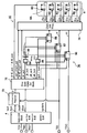
- FIG. 2 is a block diagram of the TAP controller 4, the scan storage element group 6, and the control circuit of FIG.
- an instruction register (Instruction Register) 70 a data scan chain selection circuit (Data Scan Chain Select Block) 72, a chain control circuit (Chain Control Block) 74, and a data setting circuit 76 are connected to the TAP controller (in the figure).
- (Scan Cntl Block) 4 and the scan storage element group 6 are provided.
- the instruction register 70 is composed of a shift register and stores an instruction (for example, a mode instruction) from the TDI signal line.
- the data scan chain selection circuit 72 instructs the chain control circuit 74 to use the uni chain or the user chain by the signal uni_chain_sel and the signal AE_chain_sel.
- the scan storage element group 6 is divided into a plurality of blocks 6A, 6B, 6C, 6D, and 6E.
- Each block 6A, 6B, 6C, 6D, 6E has a number of FFs 60 connected in a chain.
- Each block 6A, 6B, 6C, 6D, 6E is connected to the chain control circuit 74, receives inputs Asi, Bsi, Csi, Dsi, Esi from the chain control circuit 74, and chains outputs Aso, Bso, Cso, Dso, Eso. Output to the control circuit 74.
- the chain selection circuit 74 When uni-chain is instructed from the data scan chain selection circuit (Data Scan Chain Select Block) 72, the chain selection circuit 74 connects all the blocks 6A, 6B, 6C, 6D, and 6E. The data of the FF 60 of the block is shifted. When a user chain is instructed, the chain selection circuit 74 shifts the data of each FF 60 for each block 6A, 6B, 6C, 6D, 6E. Unichain is a chain that connects all user chains (each block).
- the data setting circuit 76 includes a start code register 80, an end code register 82, a bypass setting register 88, a data register 86, an address register 84, and an address decoder 90.
- the start code register 80, the end code register 82, the bypass setting register 88, the data register 86, and the address register 84 are each composed of a shift register.
- a start code register 80 for holding a start code is provided between the chain control circuit 74 and the output signal line TDO.
- An end code register 82 for holding an end code is provided between the chain control circuit 74 and the input signal line TDI.
- the bypass setting register 88 holds data specifying a block (chain) to be bypassed and is connected to the chain control circuit 74.
- the data register 86 holds data (start code, end code, bypass setting data) from the input signal line TD 1 and writes it in each of the start code register 80, end code register 82, and bypass setting register 88.
- the address register 84 holds an address (start code register address, end code register address, bypass setting data register address) from the input signal line TD1.
- the address decoder 90 decodes the address of the address register 84 and outputs an instruction to write to each of the start code register 80, end code register 82, and bypass setting register 88.
- the start code of the start code register 80 is first output to the output signal line TDO (referred to as shift-out) during scanning.
- the end code of the end code register 82 is finally shifted out to the signal line TDO.
- the chain control circuit 74 bypasses the chain (block) set to “1” by the bypass setting data in the bypass setting register 88.
- the data register 86 and the address register 84 are accessible only during scanning.
- the TAP controller 4 sets an address register selection code in the instruction register 70. That is, the TAP controller 4 receives the mode instruction from the signal line TMS and supplies the shift clocks iack and ibck to the instruction register 70.
- the instruction register 70 takes in (scans in) input data (address register selection code) of the input signal line TDI by the supplied clocks iack and ibck.
- the TAP controller 4 sets the write address of the start code register 80, end code register 82, and bypass setting register 88 in the address register 84. That is, the TAP controller 4 supplies the shift clocks dack and dbck to the data scan chain selection circuit 72.
- the data scan chain selection circuit 72 supplies shift clocks jir_ack and jir_bck to the address register 84 according to the instruction code ir of the instruction register 70.
- the address register 84 takes in (scans in) input data (address data of each register) of the input signal line TDI by the supplied shift clocks jir_ack and jir_bck.
- the TAP controller 4 sets a data register selection code in the instruction register 70. That is, the TAP controller 4 receives the mode instruction from the signal line TMS and supplies the shift clocks iack and ibck to the instruction register 70.
- the instruction register 70 takes in (scans in) the input data (data register selection code) of the input signal line TDI by the supplied shift clocks iack and ibck.
- the TAP controller 4 sets the write data of the start code register 80, the end code register 82, and the bypass setting register 88 in the data register 86. That is, the TAP controller 4 supplies the shift clocks dack and dbck to the data scan chain selection circuit 72.
- the data scan chain selection circuit 72 supplies the shift clocks jdr_ack and jdr_bck to the data register 86 according to the instruction code ir of the instruction register 70.
- the data register 86 takes in (scans in) input data (write data of each register) of the input signal line TDI by the supplied shift clocks jdr_ack and jdr_bck.
- the TAP controller 4 issues an update signal (update) to each of the start code register 80, the end code register 82, and the bypass setting register 88 after the shift to the data register 86 is completed. Since the address decoder 90 decodes the register address held in the address register 84 and supplies a selection signal to each of the start code register 80, the end code register 82, and the bypass setting register 88, the start code register 80, The corresponding write data held in the data register 86 is written in the end code register 82 and the bypass setting register 88.
- the TAP controller 4 receives a mode instruction from the signal line TMS and supplies shift clocks iack and ibck to the instruction register 70.
- the instruction register 70 takes in (scans in) the input data (uni-chain mode selection code) of the input signal line TDI by the supplied shift clocks iack and ibck.
- the TAP controller 4 supplies shift clocks dack and dbck to the data scan chain selection circuit 72.
- the data scan chain selection circuit 72 recognizes the unichain instruction by the instruction code ir of the instruction register 70, supplies the shift clocks A-E_ack and A-E_bck to the scan storage element group 6, and the start code register 80 and the end code register 82. Shift clocks ack and bck are supplied.
- the data scan chain selection circuit 72 issues a unichain selection signal (here, the signal AE_chain_sel is off “0”) to the chain control circuit 74.
- Each FF 60 in the scan storage element group 6 performs a shift operation by the supplied shift clocks AE_ack and AE_bck, and scans data in and out to the output signal line TDO via the chain control circuit 74.
- a start code is added to the head of the scanned data.
- the end code of the end code register 82 is input to the first FF 60 of the scan storage element group 6 via the chain control circuit 74, the end code is added to the end of the scanned data.
- the scan data to which the start code and end code are added is sent from the output signal line TDO to the JTAG control board 30 of the host computer 3 via the dedicated cable 34 and stored in the memory 32 (see FIG. 1).
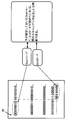
- FIG. 3 is an explanatory diagram of the collected data of FIG.
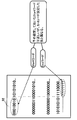
- FIG. 4 is an explanatory diagram of other collected data of FIG.
- FIG. 5 is an explanatory diagram of the collected data analysis of the comparative example.
- FIG. 6 is another explanatory diagram of the collected data analysis of the comparative example.
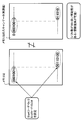
- FIG. 7 is an explanatory diagram of an analysis example based on the collected data of FIG.
- FIG. 8 is an explanatory diagram of another analysis example based on the collected data of FIG.
- the scan data in the memory 32 has a start code at the beginning and an end code at the end.
- the scan data on the memory 32 is output.
- the person in charge of debugging looks at the output result and can determine that the scan data between them is correct if the preset start code and end code are included.
- the start code and end code can be set to arbitrary values. As shown in FIG. 4, since the scan data is arbitrary, in the scan data, values (“00010010”) (“001110100”) similar to those before and after the start code (“00010010”) and the end code (“001110100”) are included. ) Makes it difficult to judge. In such a case, if it is difficult to read after scanning once, a start code (“00010110”) and an end code (“001110100”) having different values from the similar values before and after the start code and the end code. To obtain scan data again. Thus, regardless of the data value held in the scan storage element group 6, the person in charge of debugging looks at the output result, and if the preset start code and end code are included, the scan data between them Can be judged to be correct.
- FIG. 6 shows an example of correct / incorrect determination based on the points in the comparative example.
- a part of the scan data (“101...”) Stored in the memory MEM is expanded on a scan page ((1) in FIG. 6). That is, the analysis tool (program) is executed to develop the data (8 bits in the figure) at the point of the scan data on the scan page in register units (A-REG, B-REG, C-REG).
- FF data on the LSI in register units A-REG, B-REG, C-REG
- the read value is compared with the value on the scan page ((2) in FIG. 6).
- the scan address of the comparison point such as a register is examined to find the scan data from the memory MEM ((3) in FIG. 6).
- the FF data on the LSI is read from another interface. The read value is compared with the value of the searched data ((2) in FIG. 6).
- the expected value (set value) of the start code and end code can be used not only for correct / incorrect determination but also as information on the result considered to be incorrect.
- the start code in the scan data of the memory 32 may match the expected value (set value), and the end code may not match the expected value (set value).
- the start code since the start code does not pass through the scan storage element group 6, there is a low possibility of mismatch.
- the end code passes through the scan storage element group 6, it can be determined that there is a possibility that there is a problem in some scan chain (hardware) in the scan storage element group 6 when they do not match.
- the number of shifts set in the JTAG program is different from the number of shifts required for the target LSI. If the scan data is considered to be invalid, first, it is investigated whether it is a problem of the program that controls the JTAG or a scan chain (hardware) problem in the LSI. In this embodiment, a criterion for investigation can be given.
- FIG. 9 is a block diagram of the chain control circuit 74 and the scan storage element group 6 described in FIG.
- FIG. 10 is an explanatory diagram of selection ethics of the selection circuit of FIG.
- FIG. 11 is an explanatory diagram of selection conditions of the selection circuit of FIG.
- FIG. 12 is an explanatory diagram of a method for identifying a fault location according to the configuration of FIG.
- the scan storage element group 6 includes five blocks (chains) 6A, 6B, 6C, 6D, and 6E. Each block 6A, 6B, 6C, 6D, 6E has a FF 60 connected in a chain (series). Blocks 6A, 6B, 6C, 6D, and 6E receive input data Asi, Bsi, Csi, Dsi, and Esi from the chain control circuit 74, and output data Aso, Bso, Cso, Dso, and Eso to the chain control circuit 74.
- the chain control circuit 74 receives the end code of the end code register 82.
- the chain control circuit 74 receives the bypass data AE_BYP in the bypass setting register 88 and the chain selection signal AE_chain_sel from the data scan chain selection circuit 72 as chain selection conditions.
- the chain control circuit 74 includes one driver circuit 78A, five chain selection circuits 78B, 78C, 78D, 78E, and 78F, and a selection signal generation circuit 76.
- the driver circuit 78A and the four chain selection circuits 78B, 78C, 78D, and 78E send input data Asi, Bsi, Csi, Dsi, and Esi to the blocks 6A, 6B, 6C, 6D, and 6E, respectively.
- the chain selection circuit 78F sends the scan output so to the output signal line TDO via the start code register (shift register) 86.
- the selection signal generation circuit 76 generates chain selection circuits 78B, 78C from the bypass data AE_BYP in the bypass setting register 88 and the chain selection signal AE_chain_sel from the data scan chain selection circuit 72 according to the selection logic shown in FIGS. Output selection signals 78D, 78E, and 78F are generated.
- the chain selection signal AE_chain_sel has a selection bit for each block A to E for selecting the output of each block A to E. As for the selection bit, “1” (ON) indicates selection, and “0” (OFF) indicates non-selection.
- the bypass data AE_BYP has a selection bit for each block A to E that bypasses each block A to E. In the selection bit, “1” (on) indicates bypass, and “0” (off) indicates non-bypass.
- the driver circuit 78A receives the input si from the input signal line TDI via the end code register (shift register) 82, and outputs the input data Asi to the block 6A.
- the first chain selection circuit 78B receives the above-described input si and the output data Aso of the block 6A, selects one by a selection signal, and outputs the input data Bsi to the block 6B.
- the second chain selection circuit 78C receives the aforementioned input si, the output data Aso of the block 6A, and the output data Bso of the block 6B, selects one by a selection signal, and outputs the input data Csi to the block 6C.
- the third chain selection circuit 78D receives the input si, the output data Aso of the block 6A, the output data Bso of the block 6B, and the output data Cso of the block 6C, selects one of them by a selection signal, and inputs it to the block 6D. Data Dsi is output.
- the fourth chain selection circuit 78E receives the input si, the output data Aso of the block 6A, the output data Bso of the block 6B, the output data Cso of the block 6C, and the output data Dso of the block 6D, and selects one of them according to the selection signal. The selected data is output to the block 6E.
- the fifth chain selection circuit 78F receives the input si, the output data Aso of the block 6A, the output data Bso of the block 6B, the output data Cso of the block 6C, the output data Dso of the block 6D, and the data Eso of the block 6E. Any one is selected by the selection signal, and the scan data so is output to the start code register 80.
- the vertical axis indicates the outputs Asi, Bsi, Csi, Dsi, Esi, and so of the driver circuit 78A and the chain selection circuits 78B to 78F
- the horizontal axis indicates the inputs si and Aso of the driver circuit 78A and the chain selection circuits 78B to 78F.
- Bso, Cso, Dso, and Eso The connection between the driver circuit 78A and the chain selection circuits 78B to 78F described above is a connection for selecting the input on the horizontal axis with a circle in the output line on the vertical axis in FIG.
- the selection signal generation circuit 76 generates selection signals for the driver circuit 78A and the chain selection circuits 78B to 78F with the logic of FIG.
- the vertical axis represents the outputs Asi, Bsi, Csi, Dsi, Esi, and so of the driver circuit 78A and the chain selection circuits 78B to 78F
- the horizontal axis represents the inputs si and Aso of the driver circuit 78A and the chain selection circuits 78B to 78F.
- Bso, Cso, Dso, and Eso The selection signal generation conditions of the selection signal generation circuit 76 are shown at the intersection of the vertical axis and the horizontal axis.
- the selection signal generation condition N in FIG. 11 means Normal in which all bits of the chain selection signal A_E_chain_sel are in an off state and all bits of the bypass data AE_BYP are in an off state and the unichain selection signal uni_chain_sel is on.
- the selection signal generation conditions A, B, C, D, and E mean that the bits of the blocks A to E of the chain selection signal A_E_chain_sel are on.
- the selection signal generation conditions a, b, c, d, and e mean that the bits of the blocks A to E of the bypass data A_E_BYP are on.
- the uni-chain selection signal uni_chain_sel is on to designate a uni-chain. Further, the “+” mark in FIG. 11 indicates the OR condition.
- the selection signal generation circuit 76 receives the bypass data AE_BYP and the chain selection signal AE_chain_sel, and generates the following selection signals for the chain selection circuits 78B to 78F.
- the chain selection circuits 78B to 78E select the previous output Aso, Bso, Cso, Dso, and the chain selection circuit 78F generates a selection signal for selecting the input si.
- each of the chain selection circuits 78B to 78E generates a selection signal for selecting the input si.
- the chain selection circuit 78F generates a selection signal for selecting the outputs Aso, Bso, Cso, Dso, and Eso corresponding to each case. As a result, the user chain is selected.
- each of the chain selection circuits 78C to 78E generates a selection signal for selecting the output Aso.
- the chain selection circuits 78D to 78E generate selection signals for selecting the output Bso corresponding to each case.
- the chain selection circuit generates a selection signal for selecting the output Cso.
- the chain control circuit 74 selects the configuration of the uni chain, the specified user chain, and the bypass chain. For example, in the case of N (in the case of Normal), the chain selection circuits 78B to 78F select the outputs Aso, Bso, Cso, Dso, Eso of the preceding blocks A, B, C, D, E, Form a unichain.
- chain selection circuit 78B selects input si, and chain selection circuit 78F outputs block B output Bso. Select. That is, a user chain including only the block 6B is formed.
- a user chain of only block 6C is formed.
- D + a + b + c and D + e in the case of selecting block D or instructing bypass of blocks A, B, C, and E
- a user chain of only block 6D is formed.
- E + a + b + c + d and N + E in the case of selection of block E or bypass instruction of blocks A, B, C, and D
- a user chain of only block 6E is formed.
- bypass block B only block B is bypassed.
- c bypass of block C
- d bypass of block C
- each chain of the scan storage element group 6 is investigated. That is, each chain A, B, C, D is scanned individually. That is, as described above, the user chain is designated to the TAP controller 4 and the chain selection signal AE_chain_sel is issued from the data scan chain selection circuit 72. At the same time, the data scan chain selection circuit 72 supplies the shift clocks AE_ack and AE_bck to the scan storage element group 6, and supplies the shift clocks ack and bck to the start code register 80 and the end code register 82 (FIG. 12). P2).
- This scans in user chain units collects scan data with start codes and end codes added in user chain units, and stores them in the memory (S2 in FIG. 12).
- the data surrounded by a dotted line is a start code and an end code.
- the user chain bypass data shown in FIG. 11 is written to the chain bypass register 88, and the data scan chain selection circuit 72 supplies the shift clocks AE_ack and AE_bck to the scan storage element group 6, and the start code register 80 and end Shift clocks ack and bck are supplied to the code register 82.
- the uni-chain scan data of the chains A, B, and D excluding the bypassed chain C is collected in the memory (S3 in FIG. 12).
- S3 of FIG. 12 since the start code and the end code (data surrounded by a dotted line in FIG. 12) appear at the beginning of the uni-chain scan data of the chains A, B, and D, the chains A, B, D can be determined to be normal.
- a bit that can be controlled in user chain units is provided in the bypass register, and scanning is performed in the unichain mode after setting the bypass. This allows scanning by bypassing the problem chain set by the circuits forming the unichain.
- debugging efficiency is improved.
- debug quality is improved.
- debugging efficiency is improved because information can be provided at the time of investigation.
- FIG. 13 is a block diagram of an embodiment of an information processing apparatus to which the debug system of FIGS. 1 and 2 is applied.
- the information processing apparatus in FIG. 13 represents a server system.
- the server system includes a plurality of system boards (SB: System Board) 1A to 1D as processing devices, a management board (MMB: Management Ment Board) 3 as a system control device (SVP), and a crossbar.
- SB System Board
- MMB Management Ment Board
- SVP system control device
- IOUs input output units
- the system boards 1A to 1D correspond to the board 1 in FIG. 1, and the management board 3 corresponds to the host computer 3 in FIG.
- Each of the system boards 1A to 1D is provided on a circuit board with a CPU (Central Processing Unit) 5A as an arithmetic processing unit, a memory controller 5B, a memory 14 as a main storage device, a bridge circuit 18, and a network interface circuit (NIC: (Network Interface Card) 16.
- NIC Network Interface Card
- the NICs 16 of the system boards 1A to 1D are connected to the management board 3 via an internal bus 8A such as a LAN (Local Area Network).
- the management board 3 performs status monitoring, start / stop control, etc. of the system boards 1A to 1D via the internal bus 8A.
- the system boards 1A to 1D are connected to the IOUs 9A to 9N by crossbar switches (or switches) 8B.
- the IOUs 9A to 9N are equipped with IO devices such as LAN devices and storage controllers.
- IO devices such as LAN devices and storage controllers.
- the crossbar switch 8B By appropriately setting the crossbar switch 8B, the system can be logically divided into a plurality of systems, and system board resources and IOU resources can be freely assigned according to the scale of the operating system.
- the CPU 5A In each of the system boards 1A to 1D, the CPU 5A, the memory controller 5B, the TAP controller 4 described with reference to FIGS. Although omitted in FIG. 13, the instruction register 70, the data scan chain selection circuit 72, the chain control circuit 74, the data setting circuit 76, and the scan storage element group 6 described in FIG.
- CPU 5A connects to memory 14 via memory controller 5B.
- the memory controller 5B and the NIC 16 are connected to the bridge circuit 18.
- the CPU 5A executes a desired application program and performs business processing based on the operation of the OS. Further, the CPU 5A communicates commands and data with the IOUs 9A to 9N through the bridge circuit 18 and through the crossbar switch 8B.
- the bridge circuit 18 is connected to the NIC 16 and the crossbar switch 8B. That is, the bridge circuit 18 performs a bridge function for connecting the CPU 5A, the crossbar switch 8B, and the NIC 16.
- the terminal device 8C is constituted by, for example, a personal computer (PC: Personal Computer), is connected to the MMB 5, instructs various settings by selecting items on the screen of the personal computer, and displays the acquired data of the MMB 5.
- PC Personal Computer
- the MMB 3 is connected to the connectors 12 of the system boards 1A to 1D by the dedicated cable 34 via the JTAG controller 30.
- the connector 12 is connected to the TAP controller 4 of the LSI 10. That is, the debug system described with reference to FIGS. 1 and 2 is provided in the server system. Therefore, the function test of the LSI 10 described with reference to FIGS. 1 to 12 can be executed in a state where the LSI 10 is mounted on the boards 1A to 1D.
- the person in charge of debugging operates the terminal device 8C, collects the state (scan data) of the FF in the LSI 10 from the JTAG controller 30, and stores it in the memory 32.
- the person in charge of debugging displays or prints the collected data in the memory 32 on the screen of the terminal device 8C or an associated printer. By looking at the output result, the person in charge makes a correct / incorrect determination as to whether the scan has been executed normally and whether the collected data is correct.
- an LSI function test can be performed to contribute to the search for the cause of the failure.
- hundreds of thousands of scan data are collected by a scan test. Therefore, it is easy and correct / error determination with less man-hours can make debugging work more efficient.
- the scan storage element has been described using the flip-flop as an example, but other shiftable storage elements can be applied.
- the scan test method has been described by the method of the JTAG standard, a scan method using another dedicated path can be applied.
- the example in which the bypass function is provided has been described, one without the bypass function can also be applied.
- An end code register is provided at the input stage of the scan storage element group, and a start code register is provided at the output stage. In order to scan, it is determined whether the scanned data includes a start code and an end code. Can be easily determined.
- Circuit board 3 Host computer (system controller) 4 TAP controller 5 Internal circuit 6 Scan storage element group 10 LSI 12 Connector 30 JTAG controller 32 Memory 6A to 6E Block 60 Scan element 70 Instruction register 72 Data scan chain selection circuit 74 Chain selection circuit 80 Start register 82 End register 88 Bypass register 38 Internal bus
Landscapes
- Engineering & Computer Science (AREA)
- General Engineering & Computer Science (AREA)
- Physics & Mathematics (AREA)
- General Physics & Mathematics (AREA)
- Tests Of Electronic Circuits (AREA)
- Test And Diagnosis Of Digital Computers (AREA)
Abstract
複数のスキャン記憶素子を直列接続したスキャン記憶素子群をスキャンしてデータ収集する際に、収集データの正誤判定を容易とする。複数段のスキャン記憶素子を直列に接続したスキャン記憶素子群(6)と、入力端とスキャン記憶素子群(6)の入力側との間に設けられ、エンドコードを保持するエンドコードレジスタ(82)と、出力端とスキャン記憶素子群(6)の出力側の間に設けられ、スタートコードを保持するスタートコードレジスタ(80)と、スキャン記憶素子群(6)とエンドコードレジスタ(82)とスタートコードレジスタ(80)とをシフト動作させ、出力端にスキャンデータを出力する。
Description
本発明は、半導体集積回路装置、その制御方法及び情報処理装置に関する。
半導体集積回路(Semiconductor Integrated Circuit)の集積度の向上に伴い、半導体集積回路は多数の回路素子を搭載している。特に、大規模集積回路(LSI:Large Scale Integrated Circuit)は数十万、数百万の回路素子を搭載している。大規模集積回路(以下、LSIという)の機能試験は、内部回路の調査、解析及び確認を行うために有効である。
バウンダリスキャンテスト(Boundary Scan Test)はLSIの内部回路の動作テストやプリント基板にLSIを実装した後のボードテストとして利用されている。IEEE1149.1(IEEE:The Institute of Electrical and Electronic Engineers, Inc.)で企画されたJTAG(Joint Test Action Group)によるテスト方法はバウンダリスキャンテストの代表例である。
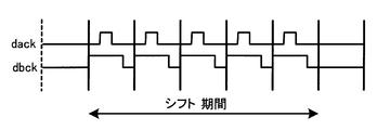
図14はJTAGによるスキャンテストの構成図である。図15は図14の制御信号のタイムチャート図である。図14に示すように、テスト対象ロジック回路200は複数のフリップフロップ回路(Flip Flop Circuit)200-1~200-Mにより構成されている。これらのフリップフロップ回路(以下、FFという)200-1~200-Mは直列接続される(スキャンチェーンという)。このFFはセル(Cell)の一種であり、一般に、シフトレジスタとラッチ回路とを有する。
JTAGスキャン方法はテストロジック回路200に対しテスト専用のパスを設ける。外部装置からの信号線はTDI(Test Data In)、TDO(Test Data Out)、TCK(Test Clock)、TMS(Test Mode Select)、TRST(Test Reset)である。TDIはテストロジック回路200(200-1~200-M)に対して命令やデータをシリアル入力する信号である。TDOはテストロジック回路200(200-1~200-M)からのデータをシリアル出力する信号である。
TCKはテストロジック回路200(200-1~200-M)にクロックを供給する。TMSはテスト動作を制御する信号である。TRSTはTAP(Test Access Port)コントローラ210(後述する)を非同期に初期化する信号である。
TAPコントローラ210は取り込み(キャプチャ(Capture))、シフト(Shift)、更新(アップデート(Update))を主要動作とするステートマシンである。TAPコントローラ210は信号線TMSを介するモード指定起動を受ける。そして、TAPコントローラ210は、図示しない命令レジスタにTDIからのモード命令をセットする。
TAPコントローラ210は図15に示すようなシフトクロックdack,dbckを各FF200-1~200-Mに供給する。このシフトクロックdack、dbckにより、各FF200-1~200-Mはデータのシフトレジスタへの取り込み、シフトレジスタの内容の出力、ラッチ回路への固定を行う。
TAPコントローラ210はFF200-1~200-Mにシフトクロックdack、dbckを供給し、データを順次次段のFF200-2~200-Mにシフトし、信号線TDOから出力し、スキャンテストしていた。
一方、半導体集積回路自体のテスト方法として、テスト装置がシリアルテストパターンを多段のFFで構成されたロジック回路に入力し、ロジック回路の出力を取り込み、入力したシリアルテストパターンが得られるかを判定していた。この方法は半導体集積回路の出荷前にロジック回路内の各FFの動作自体が正常であるかを試験する方法として有効である。
バウンダリスキャンテスト(Boundary Scan Test)はLSIの内部回路の動作テストやプリント基板にLSIを実装した後のボードテストに有効であり、LSIの機能試験であるデバッグ(debug)に利用されている。デバッグはある機能試験を実行した後に内部回路の調査、解析及び確認を行う。このため、FF200-1~200-Mの保持しているデータを取り出すことが有効である。
スキャンテストは単にFF200-1~200-Mの保持しているデータを取り出していたため、数十万もの回路素子の保持データを解析するのは難しい。例えば、LSI機能試験の初期段階においては、スキャンが正常に実行されたか否か、又、取得したデータが正しいか否かの正誤判断が必要である。この正誤判断は長時間の工数を必要とする。例えば、1か所でもFF間の断線やFFの動作の不良があると、取得したデータから故障個所を判断するために長時間の解析が必要である。
又、テスト装置からシリアルテストパターンをロジック回路へ入力する方法はFF200-1~200-Mの保持しているデータを無視するため、LSIのデータの正誤判断が困難である。
本発明の目的は、チェーン接続されたスキャン記憶素子からのスキャンデータの正誤を容易に判断できる半導体集積回路装置、その制御方法及び情報処理装置を提供することにある。
この目的の達成のため、開示の半導体集積回路装置は、複数段のスキャン記憶素子を直列に接続したスキャン記憶素子群と、入力端と前記スキャン記憶素子群の入力側との間に設けられ、エンドコードを保持するエンドコードレジスタと、出力端と前記スキャン記憶素子群の出力側の間に設けられ、スタートコードを保持するスタートコードレジスタと、前記スキャン記憶素子群と前記エンドコードレジスタと前記スタートコードレジスタとをシフト動作させ、前記出力端にスキャンデータを出力するスキャン制御回路とを有する。
又、開示の半導体集積回路装置の制御方法は、複数段のスキャン記憶素子を直列に接続したスキャン記憶素子群をシフト動作させ、前記スキャン記憶素子のデータを収集する制御方法において、入力端と前記スキャン記憶素子群の入力側との間に設けられ、エンドコードを保持するエンドコードレジスタと、出力端と前記スキャン記憶素子群の出力側の間に設けられ、スタートコードを保持するスタートコードレジスタと、前記スキャン記憶素子群とをシフト動作する工程と、前記出力端にスキャンデータを出力する工程とを有する。
更に、開示の情報処理装置は、情報処理を行う半導体集積回路を有する処理装置と、前記処理装置を監視するシステム制御装置とを有し、前記半導体集積回路は、前記情報処理を実行する機能回路と、複数段のスキャン記憶素子を直列に接続したスキャン記憶素子群と、前記システム制御装置と接続された入力端と前記スキャン記憶素子群の入力側との間に設けられ、エンドコードを保持するエンドコードレジスタと、前記システム制御装置に接続された出力端と前記スキャン記憶素子群の出力側の間に設けられ、スタートコードを保持するスタートコードレジスタと、前記スキャン記憶素子群と前記エンドコードレジスタと前記スタートコードレジスタとをシフト動作させ、前記出力端にスキャンデータを出力するスキャン制御回路とを有する。
スキャン記憶素子群の入力段にエンドコードレジスタを、出力段にスタートコードレジスタを設け、スキャンするため、スキャンされたデータにスタートコードとエンドコードが含まれているかを判別して、スキャンデータの正誤を容易に判断できる。
以下、実施の形態の例を、デバッグシステム、半導体集積回路装置、半導体集積回路装置の制御方法、障害個所の特定方法、情報処理装置、他の実施の形態の順で説明するが、開示の半導体集積回路装置、情報処理装置は、この実施の形態に限られない。
(デバッグシステム)
図1は、実施の形態のデバッグシステムの構成図である。図2は、図1の半導体集積回路装置のブロック図である。以下、デバッグシステムをJTAG規格のシステムの例で説明する。図1に示すように、デバッグ対象の半導体集積回路装置(以下、LSIという)10とJTAGコネクタ12とが回路基板(以下、ボードという)1に搭載されている。ボード1のJTAGコネクタ12は専用ケーブル(信号線)34を介しホストコンピュータ3に設けられたJTAGコントローラボード30に接続する。
図1は、実施の形態のデバッグシステムの構成図である。図2は、図1の半導体集積回路装置のブロック図である。以下、デバッグシステムをJTAG規格のシステムの例で説明する。図1に示すように、デバッグ対象の半導体集積回路装置(以下、LSIという)10とJTAGコネクタ12とが回路基板(以下、ボードという)1に搭載されている。ボード1のJTAGコネクタ12は専用ケーブル(信号線)34を介しホストコンピュータ3に設けられたJTAGコントローラボード30に接続する。
LSI10は内部ロジック回路5とスキャン記憶素子群6とTAPコントローラ4とを有する。スキャン記憶素子群6はチェーン接続された多数のスキャン記憶素子60を有する。内部ロジック回路5は、種々の機能を実行する論理回路で構成され、例えば、演算処理装置やメモリコントローラである。スキャン記憶素子60は、内部ロジック回路5の各部のデータを保持する記憶素子で構成され、例えば、シフトレジスタとラッチ回路とを有するフリップフロップ回路で構成される。
専用ケーブル34はTDI(Test Data In)、TDO(Test Data Out)、TCK(Test Clock)、TMS(Test Mode Select)、TRST(Test Reset)の各信号線を有する。TDIはスキャン記憶素子(以下、FFという)60に対して命令やデータをシリアル入力する入力信号線である。TDOはFF60からのデータをシリアル出力する出力信号線である。
TCK信号線はTAPコントローラ4にクロックを供給する。TMS信号線はTAPコントローラ4にテスト動作を制御する信号線である。TRST信号線はTAPコントローラ4を非同期に初期化する信号線である。TAPコントローラ4は取り込み(キャプチャ(Capture))、シフト(Shift)、更新(アップデート(Update))を主要動作とするステートマシンである。
ホストコンピュータ3は図示しない演算処理装置とJTAGコントローラボード30とメモリ32とを有する。JTAGコントローラボード30はJTAGコントローラを搭載する。JTAGコントローラは専用ケーブル34を介しコネクタ12とシリアルデータの入出力の制御を行い、且つTMS信号、TCK信号を制御する。
このように、LSI10をボード1に搭載した状態で、ホストコンピュータ3がLSI10の機能試験を行う。この機能試験の初期段階でLSI10内部のFF60をスキャンし、FF60のデータを収集する。収集データはホストコンピュータ3のメモリ32に格納される。このメモリ32の収集データを出力し、出力から収集データの正誤判定や故障個所の発見等に利用する。
(半導体集積回路装置)
図2は図1のTAPコントローラ4、スキャン記憶素子群6及び制御回路のブロック図である。
図2は図1のTAPコントローラ4、スキャン記憶素子群6及び制御回路のブロック図である。
図2において、図1で示したものと同一のものは同一の記号で示してある。図2に示すように、インストラクションレジスタ(Instruction register)70とデータスキャンチェーン選択回路(Data Scan Chain Select Block)72とチェーン制御回路(Chain Control Block)74とデータ設定回路76とがTAPコントローラ(図ではScan Cntl Blockと記す)4とスキャン記憶素子群6との間に設けられる。
インストラクションレジスタ70はシフトレジスタで構成され、TDI信号線からの命令(例えば、モード命令)を格納する。データスキャンチェーン選択回路72はインストラクションレジスタ70の命令に応じて、信号uni_chain_selと信号A-E_chain_selによって、ユニチェーン又はユーザーチェーンをチェーン制御回路74に指示する。
スキャン記憶素子群6は複数のブロック6A、6B、6C、6D,6Eに分割される。各ブロック6A、6B、6C、6D,6Eはチェーン接続された多数のFF60を有する。各ブロック6A、6B、6C、6D,6Eはチェーン制御回路74に接続され、入力Asi、Bsi,Csi,Dsi,Esiをチェーン制御回路74から受け、出力Aso、Bso,Cso,Dso,Esoをチェーン制御回路74に出力する。
データスキャンチェーン選択回路(Data Scan Chain Select Block)72からユニチェーン(uni-chain)が指示された時は、チェーン選択回路74は各ブロック6A、6B、6C、6D,6Eを全て接続し、各ブロックのFF60のデータをシフトする。ユーザーチェーン(user Chain)が指示された時は、チェーン選択回路74はブロック6A、6B、6C、6D,6E毎に各FF60のデータをシフトする。ユニチェーンとはユーザーチェーン(各ブロック)を全て接続し、1本のチェーンにしたものである。
又、データ設定回路76は、スタートコードレジスタ80とエンドコードレジスタ82とバイパス設定レジスタ88とデータレジスタ86とアドレスレジスタ84とアドレスデコーダ90とを有する。スタートコードレジスタ80とエンドコードレジスタ82とバイパス設定レジスタ88とデータレジスタ86とアドレスレジスタ84とが各々シフトレジスタで構成される。
スタートコードを保持するスタートコードレジスタ80がチェーン制御回路74と出力信号線TDOとの間に設けられる。エンドコードを保持するエンドコードレジスタ82がチェーン制御回路74と入力信号線TDIとの間に設けられる。バイパス設定レジスタ88はバイパスすべきブロック(チェーン)を指定するデータを保持し、チェーン制御回路74に接続する。
データレジスタ86は入力信号線TD1からのデータ(スタートコード、エンドコード、バイパス設定データ)を保持し、スタートコードレジスタ80,エンドコードレジスタ82,及びバイパス設定レジスタ88の各々に書き込む。アドレスレジスタ84は入力信号線TD1からのアドレス(スタートコードレジスタアドレス、エンドコードレジスタアドレス、バイパス設定データレジスタアドレス)を保持する。アドレスデコーダ90はアドレスレジスタ84のアドレスをデコードし、スタートコードレジスタ80,エンドコードレジスタ82,及びバイパス設定レジスタ88の各々に書き込む指示を出力する。
この構成により、スキャン時にスタートコードレジスタ80のスタートコードが最初に出力信号線TDOに出力(シフトアウトという)される。又、スキャン時にエンドコードレジスタ82のエンドコードが最後に信号線TDOにシフトアウトされる。チェーン制御回路74はバイパス設定レジスタ88のバイパス設定データにより「1」を設定されたチェーン(ブロック)をバイパスする。尚、データレジスタ86とアドレスレジスタ84とはスキャン時のみアクセス可能なレジスタである。
(半導体集積回路装置の制御方法)
図2を用いて、スタートコードレジスタ80,エンドコードレジスタ82,及びバイパス設定レジスタ88へのデータの設定動作を説明する。先ず、TAPコントローラ4は、インストラクションレジスタ70にアドレスレジスタ選択のコードを設定する。即ち、TAPコントローラ4は信号線TMSからのモード指示を受け、インストラクションレジスタ70にシフトクロックiack,ibckを供給する。インストラクションレジスタ70は供給されたクロックiack,ibckにより入力信号線TDIの入力データ(アドレスレジスタ選択のコード)を取り込む(スキャンインする)。
図2を用いて、スタートコードレジスタ80,エンドコードレジスタ82,及びバイパス設定レジスタ88へのデータの設定動作を説明する。先ず、TAPコントローラ4は、インストラクションレジスタ70にアドレスレジスタ選択のコードを設定する。即ち、TAPコントローラ4は信号線TMSからのモード指示を受け、インストラクションレジスタ70にシフトクロックiack,ibckを供給する。インストラクションレジスタ70は供給されたクロックiack,ibckにより入力信号線TDIの入力データ(アドレスレジスタ選択のコード)を取り込む(スキャンインする)。
次に、TAPコントローラ4は、アドレスレジスタ84にスタートコードレジスタ80,エンドコードレジスタ82,及びバイパス設定レジスタ88のライトアドレスを設定する。即ち、TAPコントローラ4はデータスキャンチェーン選択回路72にシフトクロックdack,dbckを供給する。データスキャンチェーン選択回路72は、インストラクションレジスタ70の命令コードirにより、アドレスレジスタ84にシフトクロックjir_ackとjir_bckとを供給する。アドレスレジスタ84は供給されたシフトクロックjir_ackとjir_bckとにより入力信号線TDIの入力データ(各レジスタのアドレスデータ)を取り込む(スキャンインする)。
更に、TAPコントローラ4はインストラクションレジスタ70にデータレジスタ選択のコードを設定する。即ち、TAPコントローラ4は信号線TMSからのモード指示を受け、インストラクションレジスタ70にシフトクロックiack,ibckを供給する。インストラクションレジスタ70は供給されたシフトクロックiack,ibckにより入力信号線TDIの入力データ(データレジスタ選択のコード)を取り込む(スキャンインする)。
次に、TAPコントローラ4は、データレジスタ86にスタートコードレジスタ80,エンドコードレジスタ82,及びバイパス設定レジスタ88のライトデータを設定する。即ち、TAPコントローラ4はデータスキャンチェーン選択回路72にシフトクロックdack,dbckを供給する。データスキャンチェーン選択回路72は、インストラクションレジスタ70の命令コードirにより、データレジスタ86にシフトクロックjdr_ackとjdr_bckとを供給する。データレジスタ86は供給されたシフトクロックjdr_ackとjdr_bckとにより入力信号線TDIの入力データ(各レジスタのライトデータ)を取り込む(スキャンインする)。
TAPコントローラ4はデータレジスタ86へのシフト終了後に更新信号(update)をスタートコードレジスタ80,エンドコードレジスタ82,及びバイパス設定レジスタ88の各々に発行する。アドレスデコーダ90はアドレスレジスタ84に保持されたレジスタアドレスをデコードし、スタートコードレジスタ80,エンドコードレジスタ82,及びバイパス設定レジスタ88の各々に選択信号を供給しているため、当該スタートコードレジスタ80,エンドコードレジスタ82,及びバイパス設定レジスタ88にデータレジスタ86に保持された対応するライトデータが書き込まれる。
次に、スタートコードレジスタ80,エンドコードレジスタ82,及びバイパス設定レジスタ88への設定後のスキャン動作を説明する。先ず、ユニチェーンモードによる全FFのスキャンを行う場合を説明する。TAPコントローラ4は信号線TMSからのモード指示を受け、インストラクションレジスタ70にシフトクロックiack,ibckを供給する。インストラクションレジスタ70は供給されたシフトクロックiack,ibckにより入力信号線TDIの入力データ(ユニチェーンモード選択のコード)を取り込む(スキャンインする)。
TAPコントローラ4はデータスキャンチェーン選択回路72にシフトクロックdack,dbckを供給する。データスキャンチェーン選択回路72はインストラクションレジスタ70の命令コードirによりユニチェーン指示を認識し、スキャン記憶素子群6にシフトクロックA-E_ackとA-E_bckを供給し、スタートコードレジスタ80とエンドコードレジスタ82にシフトクロックackとbckを供給する。データスキャンチェーン選択回路72はチェーン制御回路74にユニチェーン選択信号(ここでは、信号A-E_chain_selがオフ「0」)を発行する。
スキャン記憶素子群6の各FF60は供給されたシフトクロックA-E_ackとA-E_bckによりシフト動作し、チェーン制御回路74を介し出力信号線TDOへデータをスキャンイン、アウトする。この時、スキャンされたデータは前述のスタートコードレジスタ80を介し出力信号線TDOに送出されるため、スキャンされたデータの先頭にスタートコードが付加される。又、エンドコードレジスタ82のエンドコードがチェーン制御回路74を介しスキャン記憶素子群6の先頭のFF60に入力されるため、スキャンされたデータの最後にエンドコードが付加される。
スタートコードとエンドコードが付加されたスキャンデータは出力信号線TDOから専用ケーブル34を介しホストコンピュータ3のJTAGコントロールボード30に送られ、メモリ32に格納される(図1参照)。
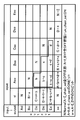
図3は図2の収集データの説明図である。図4は図2の他の収集データの説明図である。図5は比較例の収集データ解析の説明図である。図6は比較例の収集データ解析の他の説明図である。図7は図2の収集データによる解析例の説明図である。図8は図2の収集データによる他の解析例の説明図である。
図3に示すようにメモリ32のスキャンデータは先頭にスタートコード、最後尾にエンドコードを備える。このメモリ32上のスキャンデータを出力する。デバッグ担当者は、出力結果を見て、予め設定したスタートコードとエンドコードとが含まれていれば、その間のスキャンデータは正しいと判断できる。
又、スタートコードとエンドコードは任意の値に設定できる。図4に示すように、スキャンデータは任意であるため、スキャンデータ中において、スタートコード(「00010010」)とエンドコード(「00110100」)の前後に似た値(「00010010」)(「00110100」)があると判断が困難となる。このような場合に、1度スキャンした後、判読困難である場合には、スタートコードとエンドコードの前後の似た値と異なる値のスタートコード(「00010110」)とエンドコード(「00110100」)に設定し直し、再度スキャンデータを得る。これにより、スキャン記憶素子群6の保持しているデータ値に拘わらず、デバッグ担当者は、出力結果を見て、予め設定したスタートコードとエンドコードとが含まれていれば、その間のスキャンデータは正しいと判断できる。
一方、図5の比較例で示すように、LSI200のスキャンは直列でデータがシフトするため、一か所でも故障(図の×印の断線)があると、故障個所以降のデータは不正なデータとなる。即ち、収集したデータを格納したメモリMEMの内容を出力しても、図5の「X」印で示すように、故障個所以降のデータは不正なデータとなる。このため、全データ(例えば、数十万ビット)中のポイント個所のみの確認では、正誤判定に不十分である。また、多くのポイントを確認し、調査するには、数日かかる場合もあり効率が悪い。
例えば、図6に比較例のポイント個所による正誤判定の例を示す。メモリMEMに保存されたスキャンデータ(「101…」)の一部をスキャンページに展開する(図6の(1))。即ち、解析ツール(プログラム)を実行して、スキャンページ上にスキャンデータのポイント個所のデータ(図では8ビット)をレジスタ単位(A-REG、B-REG、C-REG)で展開する。次に、レジスタ単位(A-REG、B-REG、C-REG)のLSI上のFFのデータを他のインタフェースからリードする。そのリード値とスキャンページ上の値とを比較する(図6の(2))。
又、メモリMEMに保存されたスキャンデータ(「01…」)をそのまま使用する場合には、レジスタなど比較ポイントのスキャンアドレスを調べて、メモリMEMからスキャンデータを探し(図6の(3))、同様にLSI上のFFのデータを他のインタフェースからリードする。そのリード値と探したデータの値とを比較する(図6の(2))。
このように、スキャンして収集したデータは膨大(数十万ビット)であるため、全部のFFを上記の方法で確認するのは不可能である。従って、比較確認個所が残る(図6の(4))。
スタートコードとエンドコードの期待値(設定値)は正誤判定のみでなく、不正と思われる結果の情報としても使用できる。
図7に示すように、メモリ32のスキャンデータ中のスタートコードが期待値(設定値)と一致し、エンドコードが期待値(設定値)と不一致となる場合がある。図2の構成で説明したように、スタートコードは、スキャン記憶素子群6を通過しないため、不一致となる可能性は低い。一方、エンドコードはスキャン記憶素子群6を通過するため、不一致となった場合に、スキャン記憶素子群6のどこかのスキャンチェーン(ハード)に問題がある可能性があると判断できる。
更に、図8に示すように、実測したスタートコード(「00001001」)とエンドコード(「011010」)が、スタートコードの期待値(「0001010」=0x12)とエンドコード(「00110100」)の期待値と一致しないが、似た値が見える場合は、スキャン時の設定シフト数(プログラム)に問題がある可能性があると判断できる。図8では、シフト数が1ビット多い可能性がある。
即ち、JTAGプログラムで設定したシフト数が対象LSIに必要なシフト数と異なることを分析できる。スキャンデータが不正と思われる場合、最初にJTAGを制御するプログラムの問題なのか、LSI内部のスキャンチェーン(ハード)の問題なのか調査する。この実施の形態では、調査の判断基準を与えることができる。
(障害個所の特定方法)
次に、図2のバイパス設定レジスタ88及びユーザーチェーンを用いたスキャンデータの収集を説明する。図9は図2で記載したチェーン制御回路74及びスキャン記憶素子群6のブロック図である。図10は図9の選択回路の選択倫理の説明図である。図11は図10の選択回路の選択条件の説明図である。図12は図9の構成による障害個所の特定方法の説明図である。
次に、図2のバイパス設定レジスタ88及びユーザーチェーンを用いたスキャンデータの収集を説明する。図9は図2で記載したチェーン制御回路74及びスキャン記憶素子群6のブロック図である。図10は図9の選択回路の選択倫理の説明図である。図11は図10の選択回路の選択条件の説明図である。図12は図9の構成による障害個所の特定方法の説明図である。
図9において、図2で説明したものと同一のものは同一の記号で示してある。スキャン記憶素子群6は5つのブロック(チェーン)6A、6B、6C、6D、6Eを有する。各ブロック6A、6B、6C、6D、6Eはチェーン(直列)接続されたFF60を有する。ブロック6A、6B、6C、6D、6Eはチェーン制御回路74から入力データAsi、Bsi、Csi,Dsi、Esiを受け、チェーン制御回路74にデータAso、Bso、Cso,Dso、Esoを出力する。
チェーン制御回路74はエンドコードレジスタ82のエンドコードを受ける。又、チェーン制御回路74はバイパス設定レジスタ88のバイパスデータA-E_BYPとデータスキャンチェーン選択回路72からのチェーン選択信号A-E_chain_selとをチェーン選択条件として受ける。
チェーン制御回路74は1つのドライバ回路78Aと5つのチェーン選択回路78B、78C、78D、78E、78Fと選択信号生成回路76とを有する。ドライバ回路78Aと4つのチェーン選択回路78B、78C、78D、78Eとは各々ブロック6A、6B、6C、6D、6Eに入力データAsi、Bsi、Csi,Dsi、Esiを送出する。
チェーン選択回路78Fはスタートコードレジスタ(シフトレジスタ)86を介し出力信号線TDOにスキャン出力soを送出する。選択信号生成回路76はバイパス設定レジスタ88のバイパスデータA-E_BYPとデータスキャンチェーン選択回路72からのチェーン選択信号A-E_chain_selとから図10及び図11で示す選択論理によりチェーン選択回路78B、78C、78D、78E、78Fの出力選択信号を生成する。
チェーン選択信号A-E_chain_selは各ブロックA~Eの出力を選択する各ブロックA~Eの選択ビットを有する。選択ビットは「1」(オン)が選択を示し、「0」(オフ)が非選択を示す。バイパスデータA-E_BYPは各ブロックA~Eをバイパスする各ブロックA~Eの選択ビットを有する。選択ビットは「1」(オン)がバイパスを示し、「0」(オフ)が非バイパスを示す。
ドライバ回路78Aは入力信号線TDIからの入力siをエンドコードレジスタ(シフトレジスタ)82を介し受け、ブロック6Aに入力データAsiを出力する。第1のチェーン選択回路78Bは前述の入力siとブロック6Aの出力データAsoを受け、選択信号によりいずれかを選択し、ブロック6Bに入力データBsiを出力する。
第2のチェーン選択回路78Cは前述の入力siとブロック6Aの出力データAsoとブロック6Bの出力データBsoを受け、選択信号によりいずれかを選択し、ブロック6Cに入力データCsiを出力する。第3のチェーン選択回路78Dは前述の入力siとブロック6Aの出力データAsoとブロック6Bの出力データBsoとブロック6Cの出力データCsoとを受け、選択信号によりいずれかを選択し、ブロック6Dに入力データDsiを出力する。
第4のチェーン選択回路78Eは前述の入力siとブロック6Aの出力データAsoとブロック6Bの出力データBsoとブロック6Cの出力データCsoとブロック6Dの出力データDsoとを受け、選択信号によりいずれかを選択し、ブロック6Eに入力データEsiを出力する。第5のチェーン選択回路78Fは前述の入力siとブロック6Aの出力データAsoとブロック6Bの出力データBsoとブロック6Cの出力データCsoとブロック6Dの出力データDsoとブロック6EのデータEsoとを受け、選択信号によりいずれかを選択し、スタートコードレジスタ80にスキャンデータsoを出力する。
図10において、縦軸にドライバ回路78A,チェーン選択回路78B~78Fの出力Asi、Bsi、Csi,Dsi、Esi、soを、横軸にドライバ回路78A,チェーン選択回路78B~78Fの入力si、Aso、Bso、Cso,Dso、Esoを表す。前述のドライバ回路78A,チェーン選択回路78B~78Fの接続は図10の縦軸の出力の行に○印がある横軸の入力を選択する接続である。選択信号生成回路76は、図10の論理でドライバ回路78A,チェーン選択回路78B~78Fの選択信号を生成する。
具体的に図11で説明する。図11も、縦軸にドライバ回路78A,チェーン選択回路78B~78Fの出力Asi、Bsi、Csi,Dsi、Esi、soを、横軸にドライバ回路78A,チェーン選択回路78B~78Fの入力si、Aso、Bso、Cso,Dso、Esoを表す。縦軸と横軸の交差ますに選択信号生成回路76の選択信号生成条件を示す。
図11の選択信号生成条件Nは、チェーン選択信号A_E_chain_selの全ビットがオフ状態で且つバイパスデータA-E_BYPの全ビットがオフ状態で、ユニチェーン選択信号uni_chain_selがオンのNormalを意味する。選択信号生成条件A、B,C、D、Eはチェーン選択信号A_E_chain_selのブロックA~Eのビットがオンであることを意味する。選択信号生成条件a、b,c、d、eはバイパスデータA_E_BYPのブロックA~Eのビットがオンであることを意味する。ユニチェーン選択信号uni_chain_selがオンで、ユニチェーンを指定する。又、図11中の「+」印は、オア条件を示す。
図11に従い、選択信号生成回路76はバイパスデータA-E_BYPとチェーン選択信号A-E_chain_selを受け、以下のようなチェーン選択回路78B~78Fの選択信号を生成する。
(1)Nのみの場合には、チェーン選択回路78B~78Eが前段の出力Aso、Bso、Cso,Dsoを選択し、チェーン選択回路78Fは入力siを選択する選択信号を生成する。
(2)B+a、C+a+b、D+a+b+c、E+a+b+c+dの場合は、各々チェーン選択回路78B~78Eは入力siを選択する選択信号を生成する。A+b+c+d+e、B+c+d+e、C+d+e、D+d+e、N+Eの場合は、チェーン選択回路78Fは各々の場合に対応して出力Aso、Bso、Cso,Dso、Esoを選択する選択信号を生成する。これにより、ユーザーチェーンの選択が行われる。
(3)次に、図11の黒枠のバイパスデータのみを用いた選択を説明する。b、b+c、b+c+dの場合は、各々チェーン選択回路78C~78Eは各々出力Asoを選択する選択信号を生成する。c、c+dの場合は、チェーン選択回路78D~78Eは各々の場合に対応し出力Bsoを選択する選択信号を生成する。dの場合は、チェーン選択回路が出力Csoを選択する選択信号を生成する。
これらの組み合わせにより、チェーン制御回路74はユニチェーン、指定されたユーザーチェーン、バイパスチェーンの構成を選択する。例えば、Nである場合(Normalである場合)には、チェーン選択回路78B~78Fは前段のブロックA、B、C、D、Eの出力Aso、Bso、Cso,Dso、Esoを選択するため、ユニチェーンを形成する。
又、B+a且つB+c+d+eの場合(ブロックBの選択又はブロックA,C,D、Eのバイパス指示の場合)は、チェーン選択回路78Bは入力siを選択し、チェーン選択回路78FはブロックBの出力Bsoを選択する。即ち、ブロック6Bのみのユーザーチェーンを形成する。
同様に、C+a+b且つC+d+eの場合(ブロックCの選択又はブロックA,B,D、Eのバイパス指示の場合)は、ブロック6Cのみのユーザーチェーンを形成する。D+a+b+c且つD+eの場合(ブロックDの選択又はブロックA,B,C、Eのバイパス指示の場合)は、ブロック6Dのみのユーザーチェーンを形成する。E+a+b+c+d且つN+Eの場合(ブロックEの選択又はブロックA,B,C、Dのバイパス指示の場合)は、ブロック6Eのみのユーザーチェーンを形成する。
次に、図11において黒枠で囲まれたバイパス動作を説明する。b(ブロックBをバイパス)の場合は、ブロックBのみがバイパスされる。c(ブロックCのバイパス)の場合は、ブロックCのみがバイパスされる。d(ブロックCのバイパス)の場合は、ブロックDのみがバイパスされる。
b+c(ブロックB,Cのバイパス)の場合は、ブロックB,Cがバイパスされる。c+d(ブロックC、Dのバイパス)の場合は、ブロックC、Dがバイパスされる。b+c+d(ブロックB,C、Dのバイパス)の場合は、ブロックB,C、Dがバイパスされる。
このように、チェーン記憶素子群6のブロック6A~6Eのユニチェーン形成、単一のユーザーチェーン形成、特定のブロックをバイパスしたチェーン形成が可能となる。
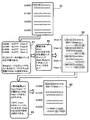
図12により故障個所の特定方法を説明する。ここでは、ブロックが4つの例で説明する。ユーザーチェーン(小さいチェーン)6A~6Dを全て接続し1本のチェーンにして、スキャンし、スキャンデータ(実測値)をメモリにログ収集する(図12のS1)。ログ収集結果において、チェーンA(図9ではブロックD)、チェーンB(図9ではブロックC)、チェーンC(図9ではブロックB),チェーンD(図9ではブロックA)のスキャンデータのメモリアドレスは、それぞれ、「0x0000―0x0FFF」、「0x1000-0x1FFF」、「0x000-0x0FFF」、「0x1000-0x1FFF」とする。又、スタートコード「00010010」は正しいものとする。
ここで、エンドコードがスキャンデータの最後に発見できない場合には、どこからデータが壊れているか不明である。又、スタートコードは正しいため、プログラムの問題ではないとは推測できる(図12のP1)。
このため、スキャン記憶素子群6の各チェーンを調査する。即ち、各チェーンA,B、C,Dを個別にスキャンする。即ち、前述のように、TAPコントローラ4にユーザーチェーンを指定し、データスキャンチェーン選択回路72からチェーン選択信号A-E_chain_selを発行する。これとともに、データスキャンチェーン選択回路72はスキャン記憶素子群6にシフトクロックA-E_ackとA-E_bckを供給し、スタートコードレジスタ80とエンドコードレジスタ82にシフトクロックackとbckを供給する(図12のP2)。
これにより、ユーザーチェーン単位でスキャンを実施し、ユーザーチェーン単位にスタートコードとエンドコードを付加されたスキャンデータを収集し、メモリに格納する(図12のS2)。図12のS2では、点線で囲まれたデータがスタートコードとエンドコードの部分である。
この収集データから各チェーンA,B,C,Dのスキャンデータに、期待値となるスタートコードとエンドコードが先頭及び最後に現れるか否かを確認する(図12のP3)。図12の例では、チェーンCの最後にエンドコードが表れていないことが判る。即ち、故障のあるチェーンを特定する。ここでは、故障チェーンCをバイパスし、チェーンA、B、Dを連結して、ログ解析する。
チェーンバイパスレジスタ88に図11で示したユーザーチェーンのバイパスデータを書き込み、データスキャンチェーン選択回路72はスキャン記憶素子群6にシフトクロックA-E_ackとA-E_bckを供給し、スタートコードレジスタ80とエンドコードレジスタ82にシフトクロックackとbckを供給する。これにより、バイパスしたチェーンCを除いたチェーンA,B、Dのユニチェーンのスキャンデータをメモリに収集する(図12のS3)。図12のS3では、チェーンA,B、Dのユニチェーンのスキャンデータの先頭にスタートコード、最後にエンドコード(図12の点線で囲まれたデータ)が表れているため、チェーンA,B、Dは正常と判定できる。
この実施の形態では、バイパスレジスタにユーザーチェーン単位で制御できるビットを設け、バイパス設定した後ユニチェーンモードでスキャンを行う。これにより、ユニチェーンを形成する回路が設定した問題チェーンをバイパスすることで、スキャンを可能にする。
このように、スキャンデータの正誤判定が一瞬でできるため、デバッグ効率が向上する。又、全収集データの確認ができるため、デバッグ品質が向上する。更に、調査時の情報提供ができるため、デバッグ効率が向上する。
(情報処理装置)
図13は図1、図2のデバッグシステムを適用した情報処理装置の一実施の形態のブロック図である。図13の情報処理装置は、サーバシステムを示す。図13において、図1及び図2で説明したものと同一のものは同一の記号で示してある。図13において、サーバシステムは、処理装置としての複数のシステムボード(SB:System Board)1A~1Dと、システム制御装置(SVP:SerVice Processor)としての管理ボード(MMB:ManageMent Board)3と、クロスバスイッチ(又はスイッチ)8Bと、複数の入出力ユニット(IOU: Input Output Unit)9A,9B,・・・9Nと、内部バス8Aと、操作端末装置8Cとを有する。
図13は図1、図2のデバッグシステムを適用した情報処理装置の一実施の形態のブロック図である。図13の情報処理装置は、サーバシステムを示す。図13において、図1及び図2で説明したものと同一のものは同一の記号で示してある。図13において、サーバシステムは、処理装置としての複数のシステムボード(SB:System Board)1A~1Dと、システム制御装置(SVP:SerVice Processor)としての管理ボード(MMB:ManageMent Board)3と、クロスバスイッチ(又はスイッチ)8Bと、複数の入出力ユニット(IOU: Input Output Unit)9A,9B,・・・9Nと、内部バス8Aと、操作端末装置8Cとを有する。
各システムボード1A~1Dは図1のボード1に対応し、管理ボード3は図1のホストコンピュータ3に対応する。各システムボード1A~1Dは回路基板に、演算処理装置としてのCPU(Central Processing Unit)5Aと、メモリコントローラ5Bと、主記憶装置としてのメモリ14と、ブリッジ回路18と、ネットワークインターフェース回路(NIC:Network Interface Card)16とを有する。
各システムボード1A~1DのNIC16は、LAN(Local Area Network)等の内部バス8Aを介し、管理ボード3に接続する。管理ボード3は、内部バス8Aを介し、各システムボード1A~1Dの状態監視、起動、停止制御等を行う。又、各システムボード1A~1Dは、クロスバスイッチ(またはスイッチ)8Bにより、IOU9A~9Nと接続する。
IOU9A~9Nは、LANデバイス、ストレージコントローラ等のIOデバイスを搭載する。クロスバスイッチ8Bを、適切に設定することで、論理的に複数のシステムに分割が可能となり、稼動するシステムの規模に応じて、自由にシステムボードのリソースとIOUのリソースを割り当てることが出来る。
各システムボード1A~1Dでは、CPU5Aとメモリコントローラ5Bと図1、図2で説明したTAPコントローラ4等を1つのLSI10に設ける。又、図13では省略したが、図2で説明したインストラクションレジスタ70とデータスキャンチェーン選択回路72とチェーン制御回路74とデータ設定回路76とスキャン記憶素子群6とがLSI10に設けられる。
CPU5Aが、メモリコントローラ5Bを介しメモリ14に接続する。メモリコントローラ5BとNIC16とがブリッジ回路18に接続する。CPU5Aは、OSの動作の元に、所望のアプリケーションプログラムを実行し、業務処理を行う。又、CPU5Aは、ブリッジ回路18を通し、クロスバスイッチ8Bを介し、IOU9A~9Nとコマンド、データの通信を行う。
ブリッジ回路18はNIC16とクロスバスイッチ8Bとに接続する。即ち、ブリッジ回路18は、CPU5Aと、クロスバスイッチ8BとNIC16との接続を行うブリッジ機能を果たす。
図1で説明したコネクタ12が各システムボード1A~1Dに設けられている。コネクタ12はLSI10のTAPコントローラ4に接続する。JTAGコントローラ30は管理ボード3に設けられる。各システムボード1A~1Dのコネクタ12は図2で説明した専用ケーブル34を介し管理ボード3のJTAGコントローラ30に接続される。端末装置8Cは、例えば、パーソナルコンピュータ(PC:Personal Computer)で構成され、MMB5に接続し、各種の設定等をパーソナルコンピュータの画面の項目選択等により指示し、且つMMB5の取得データを表示する。
従って、MMB3はJTAGコントローラ30を介し、専用ケーブル34により各システムボード1A~1Dのコネクタ12に接続する。コネクタ12はLSI10のTAPコントローラ4に接続する。即ち、図1及び図2で説明したデバッグシステムがサーバシステム内に設けられる。このため、LSI10をボード1A~1Dに搭載した状態で、図1乃至図12で説明したLSI10の機能試験を実行できる。
このため、デバッグ担当者は、端末装置8Cを操作し、JTAGコントローラ30からLSI10内部のFFの状態(スキャンデータ)を収集し、メモリ32に格納する。デバッグ担当者は、端末装置8Cの画面又は付随するプリンタにメモリ32の収集データを表示又は印刷する。この出力結果を見て、担当者は、スキャンが正常に実行されたか否か、収集データが正しいか否かの正誤判定を行う。
LSI機能試験の初期段階では、収集データに誤りがあると、JTAGプログラムの誤りか、スキャンチェーンの誤りかを判別する必要がある。本実施の形態では、JTAGプログラムの誤りか、スキャンチェーンの誤りかを判別することも容易である。又、スキャンチェーンの誤り個所を容易に判別できる。
更に、サーバシステムの出荷後も、何らかの異常が生じた場合に、LSI機能試験を行い、障害原因の探索に寄与できる。特に、LSIの複雑化に伴い、スキャンテストにより何十万のスキャンデータを収集するため、容易で工数の少ない正誤判定はデバッグ作業を効率化できる。
(他の実施の形態)
前述の実施の形態では、フリップフロップを例にスキャン記憶素子を説明したが、他のシフト可能な記憶素子を適用できる。又、スキャンテスト方法をJTAG規格の方法で説明したが、他の専用パスを使用したスキャン方法を適用できる。更に、バイパス機能を設けた例で説明したが、バイパス機能を設けないものも適用できる。
前述の実施の形態では、フリップフロップを例にスキャン記憶素子を説明したが、他のシフト可能な記憶素子を適用できる。又、スキャンテスト方法をJTAG規格の方法で説明したが、他の専用パスを使用したスキャン方法を適用できる。更に、バイパス機能を設けた例で説明したが、バイパス機能を設けないものも適用できる。
以上、本発明を実施の形態により説明したが、本発明の趣旨の範囲内において、本発明は、種々の変形が可能であり、本発明の範囲からこれらを排除するものではない。
スキャン記憶素子群の入力段にエンドコードレジスタを、出力段にスタートコードレジスタを設け、スキャンするため、スキャンされたデータにスタートコードとエンドコードが含まれているかを判別して、スキャンデータの正誤を容易に判断できる。
1 回路基板(ボード)
3 ホストコンピュータ(システム制御装置)
4 TAPコントローラ
5 内部回路
6 スキャン記憶素子群
10 LSI
12 コネクタ
30 JTAGコントローラ
32 メモリ
6A~6E ブロック
60 スキャン素子
70 インストラクションレジスタ
72 データスキャンチェーン選択回路
74 チェーン選択回路
80 スタートレジスタ
82 エンドレジスタ
88 バイパスレジスタ
38 内部バス
3 ホストコンピュータ(システム制御装置)
4 TAPコントローラ
5 内部回路
6 スキャン記憶素子群
10 LSI
12 コネクタ
30 JTAGコントローラ
32 メモリ
6A~6E ブロック
60 スキャン素子
70 インストラクションレジスタ
72 データスキャンチェーン選択回路
74 チェーン選択回路
80 スタートレジスタ
82 エンドレジスタ
88 バイパスレジスタ
38 内部バス
Claims (20)
- 複数段のスキャン記憶素子を直列に接続したスキャン記憶素子群と、
入力端と前記スキャン記憶素子群の入力側との間に設けられ、エンドコードを保持するエンドコードレジスタと、
出力端と前記スキャン記憶素子群の出力側の間に設けられ、スタートコードを保持するスタートコードレジスタと、
前記スキャン記憶素子群と前記エンドコードレジスタと前記スタートコードレジスタとをシフト動作させ、前記出力端にスキャンデータを出力するスキャン制御回路とを有する
ことを特徴とする半導体集積回路装置。 - 前記スキャン制御回路は、前記入力端からの前記スタートコードを前記スタートコードレジスタに書き込み、前記入力端からの前記エンドコードを前記エンドコードレジスタに書き込む
ことを特徴とする請求項1の半導体集積回路装置。 - 前記スキャン記憶素子群は複数段のスキャン記憶素子を直列接続した複数のブロックを有し、
前記スキャン制御回路は、単一チェーン指示に応じて、前記複数のブロックを直列接続し、個別チェーンの指示に応じて、指定されたブロックを前記エンドレジスタ及びスタートレジスタに接続する
ことを特徴とする請求項1の半導体集積回路装置。 - 前記複数のブロックの内、バイパスすべきブロックを指定するバイパスデータを保持するバイパスレジスタを更に有し、
前記スキャン制御回路は、バイパスレジスタで指定されたブロックを除く前記単一チェーンを形成する
ことを特徴とする請求項3の半導体集積回路装置。 - 前記スキャン制御回路は、前記入力端からの前記バイパスデータを前記バイパスレジスタに書き込む
ことを特徴とする請求項4の半導体集積回路装置。 - 所望の機能を実行する機能回路を更に有し、
前記スキャン記憶素子群は前記機能回路の状態を保持する
ことを特徴とする請求項1の半導体集積回路装置。 - 前記スキャン制御回路は、
単一チェーン指示に応じて、前記複数のブロックを直列接続し、個別チェーンの指示に応じて、指定されたブロックを前記エンドレジスタ及びスタートレジスタに接続するチェーン制御回路と、
前記入力端からの命令コードを解析し、前記チェーン制御回路に前記チェーン指示を与え、前記スキャン記憶素子群と前記エンドコードレジスタと前記スタートコードレジスタとをシフト動作させるクロックを供給するデータスキャン選択回路とを有する
ことを特徴とする請求項3の半導体集積回路装置。 - 前記複数のブロックの内、バイパスすべきブロックを指定するバイパスデータを保持するバイパスレジスタを更に有し、
前記データスキャン選択回路は、バイパスレジスタで指定されたブロックを除く前記単一チェーンを形成する
ことを特徴とする請求項7の半導体集積回路装置。 - 複数段のスキャン記憶素子を直列に接続したスキャン記憶素子群をシフト動作させ、前記スキャン記憶素子のデータを収集する制御方法において、
入力端と前記スキャン記憶素子群の入力側との間に設けられ、エンドコードを保持するエンドコードレジスタと、出力端と前記スキャン記憶素子群の出力側の間に設けられ、スタートコードを保持するスタートコードレジスタと、前記スキャン記憶素子群とをシフト動作する工程と、
前記出力端にスキャンデータを出力する工程とを有する
ことを特徴とする半導体集積回路装置の制御方法。 - 前記入力端からの前記スタートコードを前記スタートコードレジスタに書き込み、前記入力端からの前記エンドコードを前記エンドコードレジスタに書き込む工程を更に有する
ことを特徴とする請求項9の半導体集積回路装置の制御方法。 - 複数段のスキャン記憶素子を直列接続した複数のブロックを有する前記スキャン記憶素子群を、単一チェーン指示に応じて、前記複数のブロックを直列接続し、個別チェーンの指示に応じて、指定されたブロックを前記エンドレジスタ及びスタートレジスタに接続する工程を更に有する
ことを特徴とする請求項9の半導体集積回路装置の制御方法。 - 前記複数のブロックの内、バイパスすべきブロックを指定するバイパスデータを保持するバイパスレジスタで指定されたブロックを除く前記単一チェーンを形成する工程を更に有する
ことを特徴とする請求項11の半導体集積回路装置の制御方法。 - 前記入力端からの前記バイパスデータを前記バイパスレジスタに書き込む工程を更に有する
ことを特徴とする請求項12の半導体集積回路装置の制御方法。 - 前記スキャン記憶素子群は所望の機能を実行する機能回路の状態を保持する
ことを特徴とする請求項9の半導体集積回路装置の制御方法。 - 前記入力端からの命令コードを解析し、チェーン指示を与え、前記スキャン記憶素子群と前記エンドコードレジスタと前記スタートコードレジスタとをシフト動作させるクロックを供給する工程と、
前記チェーン指示の単一チェーン指示に応じて、前記複数のブロックを直列接続し、個別チェーンの指示に応じて、指定されたブロックを前記エンドレジスタ及びスタートレジスタに接続する工程とを更に有する、
ことを特徴とする請求項12の半導体集積回路装置の制御方法。 - 情報処理を行う半導体集積回路を有する処理装置と、
前記処理装置を監視するシステム制御装置とを有し、
前記半導体集積回路は、
前記情報処理を実行する機能回路と、
複数段のスキャン記憶素子を直列に接続したスキャン記憶素子群と、
前記システム制御装置と接続された入力端と前記スキャン記憶素子群の入力側との間に設けられ、エンドコードを保持するエンドコードレジスタと、
前記システム制御装置に接続された出力端と前記スキャン記憶素子群の出力側の間に設けられ、スタートコードを保持するスタートコードレジスタと、
前記スキャン記憶素子群と前記エンドコードレジスタと前記スタートコードレジスタとをシフト動作させ、前記出力端にスキャンデータを出力するスキャン制御回路とを有する
ことを特徴とする情報処理装置。 - 前記スキャン制御回路は、前記入力端からの前記スタートコードを前記スタートコードレジスタに書き込み、前記入力端からの前記エンドコードを前記エンドコードレジスタに書き込む
ことを特徴とする請求項16の情報処理装置。 - 前記スキャン記憶素子群を複数段のスキャン記憶素子を直列接続した複数のブロックを有し、
前記スキャン制御回路は、単一チェーン指示に応じて、前記複数のブロックを直列接続し、個別チェーンの指示に応じて、指定されたブロックを前記エンドレジスタ及びスタートレジスタに接続する
ことを特徴とする請求項16の情報処理装置。 - 前記複数のブロックの内、バイパスすべきブロックを指定するバイパスデータを保持するバイパスレジスタを更に有し、
前記スキャン制御回路は、バイパスレジスタで指定されたブロックを除く前記単一チェーンを形成する
ことを特徴とする請求項18の情報処理装置。 - 前記スキャン制御回路は、前記入力端からの前記バイパスデータを前記バイパスレジスタに書き込む
ことを特徴とする請求項19の情報処理装置。
Priority Applications (3)
| Application Number | Priority Date | Filing Date | Title |
|---|---|---|---|
| JP2012526248A JP5532134B2 (ja) | 2010-07-29 | 2010-07-29 | 半導体集積回路装置、その制御方法及び情報処理装置 |
| PCT/JP2010/062786 WO2012014303A1 (ja) | 2010-07-29 | 2010-07-29 | 半導体集積回路装置、その制御方法及び情報処理装置 |
| US13/749,079 US8667346B2 (en) | 2010-07-29 | 2013-01-24 | Semiconductor integrated circuit device, method of controlling the semiconductor integrated circuit device and information processing system |
Applications Claiming Priority (1)
| Application Number | Priority Date | Filing Date | Title |
|---|---|---|---|
| PCT/JP2010/062786 WO2012014303A1 (ja) | 2010-07-29 | 2010-07-29 | 半導体集積回路装置、その制御方法及び情報処理装置 |
Related Child Applications (1)
| Application Number | Title | Priority Date | Filing Date |
|---|---|---|---|
| US13/749,079 Continuation US8667346B2 (en) | 2010-07-29 | 2013-01-24 | Semiconductor integrated circuit device, method of controlling the semiconductor integrated circuit device and information processing system |
Publications (1)
| Publication Number | Publication Date |
|---|---|
| WO2012014303A1 true WO2012014303A1 (ja) | 2012-02-02 |
Family
ID=45529548
Family Applications (1)
| Application Number | Title | Priority Date | Filing Date |
|---|---|---|---|
| PCT/JP2010/062786 Ceased WO2012014303A1 (ja) | 2010-07-29 | 2010-07-29 | 半導体集積回路装置、その制御方法及び情報処理装置 |
Country Status (3)
| Country | Link |
|---|---|
| US (1) | US8667346B2 (ja) |
| JP (1) | JP5532134B2 (ja) |
| WO (1) | WO2012014303A1 (ja) |
Cited By (1)
| Publication number | Priority date | Publication date | Assignee | Title |
|---|---|---|---|---|
| TWI689738B (zh) * | 2019-02-21 | 2020-04-01 | 瑞昱半導體股份有限公司 | 測試系統 |
Families Citing this family (2)
| Publication number | Priority date | Publication date | Assignee | Title |
|---|---|---|---|---|
| US10642951B1 (en) * | 2018-03-07 | 2020-05-05 | Xilinx, Inc. | Register pull-out for sequential circuit blocks in circuit designs |
| DE102021122253B3 (de) * | 2021-08-27 | 2023-02-16 | Göpel electronic GmbH | Instrument zur autarken ausführung von prüfsequenzen nach jtag-standard |
Citations (3)
| Publication number | Priority date | Publication date | Assignee | Title |
|---|---|---|---|---|
| JP2000193722A (ja) * | 1998-12-28 | 2000-07-14 | Fujitsu Ltd | 半導体集積回路及び半導体試験装置 |
| JP2005249736A (ja) * | 2004-03-08 | 2005-09-15 | Advantest Corp | 試験装置及び制御方法 |
| JP2009258857A (ja) * | 2008-04-14 | 2009-11-05 | Toshiba Corp | デバッグ装置及びデバッグ方法 |
Family Cites Families (9)
| Publication number | Priority date | Publication date | Assignee | Title |
|---|---|---|---|---|
| JP2658903B2 (ja) * | 1994-10-05 | 1997-09-30 | 日本電気株式会社 | スキャンパス回路、その設計装置及びその設計方法 |
| JP3917734B2 (ja) * | 1997-11-07 | 2007-05-23 | 富士通株式会社 | 半導体記憶装置 |
| US6341092B1 (en) * | 2000-12-11 | 2002-01-22 | Lsi Logic Corporation | Designing memory for testability to support scan capability in an asic design |
| JP2006170963A (ja) | 2004-12-20 | 2006-06-29 | Fujitsu Ltd | 半導体集積回路装置のテスト回路 |
| JP5099869B2 (ja) * | 2005-02-23 | 2012-12-19 | ルネサスエレクトロニクス株式会社 | 半導体集積回路および半導体集積回路のテスト方法 |
| JP4303719B2 (ja) * | 2005-12-08 | 2009-07-29 | Necエレクトロニクス株式会社 | 半導体集積回路およびその制御方法 |
| JP2007225514A (ja) | 2006-02-24 | 2007-09-06 | Matsushita Electric Ind Co Ltd | 半導体集積回路装置及びその検査方法 |
| JP5194890B2 (ja) * | 2008-03-05 | 2013-05-08 | 富士通セミコンダクター株式会社 | 半導体集積回路 |
| US7966535B2 (en) * | 2009-02-23 | 2011-06-21 | International Business Machines Corporation | Secure scan design |
-
2010
- 2010-07-29 JP JP2012526248A patent/JP5532134B2/ja not_active Expired - Fee Related
- 2010-07-29 WO PCT/JP2010/062786 patent/WO2012014303A1/ja not_active Ceased
-
2013
- 2013-01-24 US US13/749,079 patent/US8667346B2/en not_active Expired - Fee Related
Patent Citations (3)
| Publication number | Priority date | Publication date | Assignee | Title |
|---|---|---|---|---|
| JP2000193722A (ja) * | 1998-12-28 | 2000-07-14 | Fujitsu Ltd | 半導体集積回路及び半導体試験装置 |
| JP2005249736A (ja) * | 2004-03-08 | 2005-09-15 | Advantest Corp | 試験装置及び制御方法 |
| JP2009258857A (ja) * | 2008-04-14 | 2009-11-05 | Toshiba Corp | デバッグ装置及びデバッグ方法 |
Cited By (1)
| Publication number | Priority date | Publication date | Assignee | Title |
|---|---|---|---|---|
| TWI689738B (zh) * | 2019-02-21 | 2020-04-01 | 瑞昱半導體股份有限公司 | 測試系統 |
Also Published As
| Publication number | Publication date |
|---|---|
| US8667346B2 (en) | 2014-03-04 |
| JP5532134B2 (ja) | 2014-06-25 |
| JPWO2012014303A1 (ja) | 2013-09-09 |
| US20130139016A1 (en) | 2013-05-30 |
Similar Documents
| Publication | Publication Date | Title |
|---|---|---|
| KR100989084B1 (ko) | 제어 장치 | |
| US7237161B2 (en) | Remote integrated circuit testing method and apparatus | |
| CN101141317B (zh) | 用于多jtag链的自动测试装置及方法 | |
| CN113990382B (zh) | 片上系统芯片、测试方法及测试系统 | |
| US7673188B2 (en) | System and method for controlling synchronous functional microprocessor redundancy during test and method for determining results | |
| US20090044057A1 (en) | System and Method for Controlling Synchronous Functional Microprocessor Redundancy during Test and Analysis | |
| JP2006242638A (ja) | 半導体検査装置 | |
| CN105842615A (zh) | 可于异常状态下进行调试的系统芯片及其调试方法 | |
| US7559000B2 (en) | Integrated circuit device, diagnosis method and diagnosis circuit for the same | |
| CN104569794A (zh) | 一种基于边界扫描结构的fpga在线测试仪及测试方法 | |
| US6941243B1 (en) | Using conversion of high level descriptive hardware language into low level testing language format for building and testing complex computer products with contract manufacturers without proprietary information | |
| JP5532134B2 (ja) | 半導体集積回路装置、その制御方法及び情報処理装置 | |
| JP5067266B2 (ja) | Jtag機能付き集積回路ボード | |
| CN120870819A (zh) | 一种基于现场可编程门阵列的芯片老化测试系统及方法 | |
| US7500165B2 (en) | Systems and methods for controlling clock signals during scan testing integrated circuits | |
| Ng et al. | Improving efficiency of IC burn-in testing | |
| Larsson et al. | Graceful degradation of reconfigurable scan networks | |
| TWI773140B (zh) | 用於流量捕獲及除錯工具之圖形使用者介面 | |
| US7581150B2 (en) | Methods and computer program products for debugging clock-related scan testing failures of integrated circuits | |
| TWI897830B (zh) | 一種邊界掃描測試方法及系統 | |
| JP2002196047A (ja) | Bist回路内蔵半導体集積回路装置およびテスト方法 | |
| Kis et al. | ATS-PCB: An Effective Automated Testing System for Advanced Driver Assistance Systems | |
| US20050216805A1 (en) | Methods for debugging scan testing failures of integrated circuits | |
| Gibbs | Backplane test bus applications for IEEE STD 1149.1 | |
| JP2010244174A (ja) | Dspカード試験装置およびdspカード試験装置における故障異常情報のモニタ方法 |
Legal Events
| Date | Code | Title | Description |
|---|---|---|---|
| 121 | Ep: the epo has been informed by wipo that ep was designated in this application |
Ref document number: 10855313 Country of ref document: EP Kind code of ref document: A1 |
|
| WWE | Wipo information: entry into national phase |
Ref document number: 2012526248 Country of ref document: JP |
|
| NENP | Non-entry into the national phase |
Ref country code: DE |
|
| 122 | Ep: pct application non-entry in european phase |
Ref document number: 10855313 Country of ref document: EP Kind code of ref document: A1 |