WO2012008398A1 - 電子機器および表示装置 - Google Patents
電子機器および表示装置 Download PDFInfo
- Publication number
- WO2012008398A1 WO2012008398A1 PCT/JP2011/065769 JP2011065769W WO2012008398A1 WO 2012008398 A1 WO2012008398 A1 WO 2012008398A1 JP 2011065769 W JP2011065769 W JP 2011065769W WO 2012008398 A1 WO2012008398 A1 WO 2012008398A1
- Authority
- WO
- WIPO (PCT)
- Prior art keywords
- electronic component
- substrate
- heat dissipation
- metal plate
- sheet
- Prior art date
- Legal status (The legal status is an assumption and is not a legal conclusion. Google has not performed a legal analysis and makes no representation as to the accuracy of the status listed.)
- Ceased
Links
Images





Classifications
-
- H—ELECTRICITY
- H10—SEMICONDUCTOR DEVICES; ELECTRIC SOLID-STATE DEVICES NOT OTHERWISE PROVIDED FOR
- H10W—GENERIC PACKAGES, INTERCONNECTIONS, CONNECTORS OR OTHER CONSTRUCTIONAL DETAILS OF DEVICES COVERED BY CLASS H10
- H10W40/00—Arrangements for thermal protection or thermal control
- H10W40/70—Fillings or auxiliary members in containers or in encapsulations for thermal protection or control
- H10W40/77—Auxiliary members characterised by their shape
-
- G—PHYSICS
- G02—OPTICS
- G02F—OPTICAL DEVICES OR ARRANGEMENTS FOR THE CONTROL OF LIGHT BY MODIFICATION OF THE OPTICAL PROPERTIES OF THE MEDIA OF THE ELEMENTS INVOLVED THEREIN; NON-LINEAR OPTICS; FREQUENCY-CHANGING OF LIGHT; OPTICAL LOGIC ELEMENTS; OPTICAL ANALOGUE/DIGITAL CONVERTERS
- G02F1/00—Devices or arrangements for the control of the intensity, colour, phase, polarisation or direction of light arriving from an independent light source, e.g. switching, gating or modulating; Non-linear optics
- G02F1/01—Devices or arrangements for the control of the intensity, colour, phase, polarisation or direction of light arriving from an independent light source, e.g. switching, gating or modulating; Non-linear optics for the control of the intensity, phase, polarisation or colour
- G02F1/13—Devices or arrangements for the control of the intensity, colour, phase, polarisation or direction of light arriving from an independent light source, e.g. switching, gating or modulating; Non-linear optics for the control of the intensity, phase, polarisation or colour based on liquid crystals, e.g. single liquid crystal display cells
- G02F1/133—Constructional arrangements; Operation of liquid crystal cells; Circuit arrangements
- G02F1/1333—Constructional arrangements; Manufacturing methods
- G02F1/133382—Heating or cooling of liquid crystal cells other than for activation, e.g. circuits or arrangements for temperature control, stabilisation or uniform distribution over the cell
- G02F1/133385—Heating or cooling of liquid crystal cells other than for activation, e.g. circuits or arrangements for temperature control, stabilisation or uniform distribution over the cell with cooling means, e.g. fans
-
- G—PHYSICS
- G02—OPTICS
- G02F—OPTICAL DEVICES OR ARRANGEMENTS FOR THE CONTROL OF LIGHT BY MODIFICATION OF THE OPTICAL PROPERTIES OF THE MEDIA OF THE ELEMENTS INVOLVED THEREIN; NON-LINEAR OPTICS; FREQUENCY-CHANGING OF LIGHT; OPTICAL LOGIC ELEMENTS; OPTICAL ANALOGUE/DIGITAL CONVERTERS
- G02F1/00—Devices or arrangements for the control of the intensity, colour, phase, polarisation or direction of light arriving from an independent light source, e.g. switching, gating or modulating; Non-linear optics
- G02F1/01—Devices or arrangements for the control of the intensity, colour, phase, polarisation or direction of light arriving from an independent light source, e.g. switching, gating or modulating; Non-linear optics for the control of the intensity, phase, polarisation or colour
- G02F1/13—Devices or arrangements for the control of the intensity, colour, phase, polarisation or direction of light arriving from an independent light source, e.g. switching, gating or modulating; Non-linear optics for the control of the intensity, phase, polarisation or colour based on liquid crystals, e.g. single liquid crystal display cells
- G02F1/133—Constructional arrangements; Operation of liquid crystal cells; Circuit arrangements
- G02F1/1333—Constructional arrangements; Manufacturing methods
- G02F1/1335—Structural association of cells with optical devices, e.g. polarisers or reflectors
- G02F1/1336—Illuminating devices
- G02F1/133628—Illuminating devices with cooling means
Definitions
- the present invention relates to an electronic device and a display device.
- an electronic component 101 is mounted on a mounting surface 102a of a substrate 102 as shown in FIG. Further, the metal plate 103 is disposed so as to face the mounting surface 102 a of the substrate 102, so that the electronic component 101 is covered with the metal plate 103. However, a gap is provided between the metal plate 103 and the electronic component 101.
- the heat dissipation sheet 104 for radiating the heat generated in the electronic component 101 is sandwiched in the gap between the metal plate 103 and the electronic component 101. Thereby, when the electronic component 101 generates heat, the heat is transferred to the metal plate 103 via the heat dissipation sheet 104 and radiated.
- the above-described heat radiation sheet 104 is usually manufactured by cutting a large heat radiation sheet into an appropriate size. However, when the heat radiating sheet 104 is produced in this manner, the edge portion 104a of the heat radiating sheet 104 rises more than the central portion 104b as shown in FIG.
- the edge portion 104a of the heat dissipation sheet 104 When the edge portion 104a of the heat dissipation sheet 104 is raised more than the central portion 104b, the edge portion 104a of the heat dissipation sheet 104 contacts the electronic component 101 with a high contact pressure. However, on the other hand, the contact pressure with respect to the electronic component 101 of the center part 104b of the thermal radiation sheet 104 becomes low, or the central part 104b of the thermal radiation sheet 104 does not contact with the electronic component 101. That is, the contact of the heat dissipation sheet 104 with the electronic component 101 becomes insufficient.
- the conventional electronic device has a disadvantage that the heat generated in the electronic component 101 is not efficiently dissipated even though the heat dissipating sheet 104 is used.
- the present invention has been made to solve the above-described problems, and an object of the present invention is to provide an electronic device and a display device that can dissipate heat generated in an electronic component satisfactorily.
- an electronic device faces an electronic component, a substrate having a mounting surface on which the electronic component is mounted, and a mounting surface of the substrate so as to cover the electronic component. And a heat radiating sheet disposed between the metal plate and the electronic component.
- a predetermined portion of the heat dissipation sheet that overlaps with the central portion of the electronic component when viewed in plan from the side facing the mounting surface of the substrate protrudes toward the electronic component side from the other portion of the heat dissipation sheet.
- the heat dissipation sheet is in contact with the electronic component in a state in which a predetermined portion of the heat dissipation sheet protrudes toward the electronic component side with respect to the other portion of the heat dissipation sheet.
- the central part of the electronic component in plan view (when viewed in plan from the side facing the mounting surface of the substrate) is a portion inside the edge part of the electronic component in plan view, and the electron in plan view. It is a part having an area larger than the area of the edge part of the part.
- the predetermined portion of the heat dissipation sheet that overlaps with the central portion of the electronic component in plan view projects toward the electronic component side from the other part of the heat-dissipating sheet, and with the predetermined part of the heat-dissipating sheet projecting toward the electronic component side from the other part of the heat-dissipating sheet. Projecting toward the electronic component side from the other part of the heat-dissipating sheet, and with the predetermined part of the heat-dissipating sheet projecting toward the electronic component side from the other part of the heat-dissipating sheet, The contact pressure of the heat dissipation sheet to the edge portion of the electronic component in plan view is reduced (or the heat dissipation sheet does not contact the edge portion of the electronic component in plan view).
- the contact pressure of the heat dissipation sheet with respect to the central part of the electronic component is increased. That is, the area which reliably contacts with a high contact pressure between the heat dissipation sheet and the electronic component increases. As a result, the heat generated in the electronic component is easily transmitted to the heat dissipation sheet, so that the heat generated in the electronic component can be radiated well.
- the predetermined portion of the heat dissipation sheet is bent toward the electronic component side by bending the predetermined portion of the heat dissipation sheet so as to protrude toward the electronic component side.
- the predetermined part of the thermal radiation sheet can be easily protruded toward the electronic component side.
- the predetermined surface of the metal plate is opposed to the mounting surface of the substrate, and a heat radiation sheet is attached to the predetermined surface of the metal plate. If comprised in this way, a heat dissipation sheet can be easily hold
- the predetermined portion of the heat dissipation sheet is directed toward the electronic component side. It can be bent to be convex.
- a protruding portion that protrudes toward the electronic component side is provided on a part of the metal plate, and a portion other than the portion on which the protruding portion of the metal plate is provided Is preferably flat. If comprised in this way, the predetermined part of a heat radiating sheet is affixed to the part in which the protrusion part of the metal plate was provided, and other than a part (flat part) other than the part in which the protrusion part of the metal plate was provided, By sticking this part, the predetermined part of the heat dissipation sheet can be easily bent so as to be convex toward the electronic component side.
- the protruding portion may be integrally formed on a part of the metal plate. If comprised in this way, even if it provides the protrusion part which protrudes toward the electronic component side in a part of metal plate, the number of parts does not increase.
- the metal plate is recessed so that a part of the metal plate protrudes toward the electronic component side. Is preferably in a state of being integrally formed. If comprised in this way, the protrusion part which protrudes toward the electronic component side can be easily formed integrally in a part of metal plate.
- the protruding portion may be formed of a member different from the metal plate. If comprised in this way, since the process (for example, embossing etc.) for providing a protrusion part in a part of metal plate becomes unnecessary, the manufacturing cost concerning a metal plate can be reduced.
- the projecting portion is made of a member different from the metal plate
- the projecting portion is preferably a heat conducting member. If comprised in this way, a thermal radiation characteristic will not be impaired. In this case, if a heat pipe is used as the heat conducting member, the heat dissipation characteristics can be further improved.
- the display device includes the electronic device according to the first aspect.
- the display device by configuring as described above, it is possible to easily dissipate the heat generated by the electronic components incorporated in the device easily.
- FIG. 7 is an enlarged cross-sectional view of a part of the display device according to the second embodiment shown in FIG.
- FIG. 6 (peripheral part of an electronic component mounted on a mounting surface of an inverter substrate as a substrate).
- a part of the display device according to the second embodiment shown in FIG. 6 is viewed in plan view from the side facing the mounting surface of the inverter substrate.
- FIG. It is sectional drawing which showed an example of the structure of the conventional electronic device. It is a figure for demonstrating the problem of the conventional electronic device.
- the electronic apparatus is one in which an electronic component 1 such as an IC chip that generates a large amount of heat is incorporated.
- an electronic component 1 such as an IC chip that generates a large amount of heat
- the number of electronic components 1 is not particularly limited, and may be one or plural.
- the type (function) of the electronic component 1 is not particularly limited, and can be changed according to the application.
- the electronic component 1 is mounted on the mounting surface 2 a of the substrate 2.
- substrate 2 is a glass epoxy board
- the wiring pattern (not shown) is formed in the board
- the mounting surface 2 a of the substrate 2 is protected by the substrate cover 3. That is, the electronic component 1 and the wiring pattern (not shown) are protected by the substrate cover 3.
- the substrate cover 3 is an example of the “metal plate” in the present invention.
- the substrate cover 3 is made of metal and can be obtained by processing a metal plate into a sheet metal.
- substrate cover 3 although it changes with uses, an aluminum plate, a steel plate, etc. can be considered, for example.
- the metal plate is used as the substrate cover 3 in order to increase the thermal conductivity of the substrate cover 3. That is, the substrate cover 3 has a function as a heat sink in addition to the function of protecting the electronic component 1 and the like.
- the substrate cover 3 is disposed at a predetermined interval with respect to the mounting surface 2a of the substrate 2 so as to face the mounting surface 2a of the substrate 2.
- the mounting surface 2 a of the substrate 2 is covered with the substrate cover 3, and the electronic component 1 mounted on the mounting surface 2 a of the substrate 2 is also covered with the substrate cover 3.
- the distance between the substrate cover 3 and the substrate 2 is set so that a gap is generated between the substrate 2 and the electronic component 1.
- the holding of the substrate cover 3 is not particularly limited.
- a leg (not shown) is formed on the substrate cover 3 by bending the substrate cover 3, and the leg of the substrate cover 3 is attached to the substrate.
- the method of attaching to 2 can be considered.
- the substrate cover 3 may be attached to some member (not shown).
- a heat radiation sheet 4 is disposed in the gap between the substrate cover 3 and the electronic component 1.
- the constituent material of the heat radiating sheet 4 is not particularly limited, but in addition to being excellent in heat radiating properties, it is preferably a sheet material having such a degree of flexibility that it can be easily bent.
- a silicone rubber sheet And acrylic rubber sheet for example, a silicone rubber sheet And acrylic rubber sheet.
- the thickness of the heat radiating sheet 4 is not particularly limited, but it can be easily obtained if the sheet material has a thickness of 0.3 mm to 10 mm.
- the heat dissipation sheet 4 disposed in the gap between the substrate cover 3 and the electronic component 1 is sandwiched so as to come into contact with both the substrate cover 3 and the electronic component 1. With this configuration, when the electronic component 1 generates heat, the heat is transmitted from the heat dissipation sheet 4 to the substrate cover 3 and is radiated.
- the outer size of the heat radiation sheet 4 in plan view (when viewed in plan from the side facing the mounting surface 2a of the substrate 2) is larger than the outer size of the electronic component 1 in plan view as shown in FIG. It has become. Note that the outer size of the heat dissipation sheet 4 in plan view may be the same as the outer size of the electronic component 1 in plan view, or may be smaller than the outer size of the electronic component 1 in plan view. .
- the outer shape of the heat radiation sheet 4 in a plan view is a quadrangular shape.
- this outer shape may be a shape other than a quadrangular shape (for example, a circular shape).
- the central portion of the electronic component 1 in plan view is a portion inside the edge portion of the electronic component 1 in plan view and is a portion having an area larger than the area of the edge portion of the electronic component 1 in plan view. is there.
- a protruding portion 3 a that projects toward the electronic component 1 is provided on a part of the substrate cover 3.
- the predetermined portion 4a of the heat radiating sheet 4 is projected toward the electronic component 1 side by sticking the heat radiating sheet 4 to a predetermined surface of the substrate cover 3 (a surface facing the mounting surface 2a of the substrate 2).
- the protruding portion 3a protruding toward the electronic component 1 side is provided in a part of the substrate cover 3, while the protruding portion 3a of the substrate cover 3 is provided.
- Other portions 3b are flat.
- the width W2 of the heat radiation sheet 4 is made larger than the width W1 of the protruding portion 3a of the substrate cover 3.
- substrate cover 3 and the predetermined part 4a of the thermal radiation sheet 4 overlap, and the flat part 3b of the board
- a heat radiation sheet 4 is attached to a predetermined surface of the substrate cover 3 (a surface facing the mounting surface 2a of the substrate 2).
- the shape of the heat dissipation sheet 4 is a shape that substantially reflects the uneven shape of the predetermined surface of the substrate cover 3. That is, the predetermined portion 4a of the heat dissipation sheet 4 is bent so as to be convex toward the electronic component 1 side. Thereby, it will be in the state where the predetermined part 4a of the thermal radiation sheet
- the protruding portion 3a of the substrate cover 3 is formed of a dome-shaped recess (convex portion) obtained by recessing (projecting) a part of the substrate cover 3 toward the electronic component 1 side. From this, it is clear that the protruding portion 3 a of the substrate cover 3 is not retrofitted to a part of the substrate cover 3 but is formed integrally with a part of the substrate cover 3. When a part of the substrate cover 3 is recessed (protruded) toward the electronic component 1, embossing or the like may be performed on a part of the substrate cover 3.
- the cross-sectional shape of the protruding portion 3a of the substrate cover 3 may be a semicircular shape.
- the shape may be different from the semicircular shape as long as the portion 4a can protrude toward the electronic component 1 side.
- the shape of the protruding portion 3a of the substrate cover 3 in a plan view is not particularly limited, and may be circular. It may be in the shape of a quadrangle or other shapes.
- the predetermined heat radiating sheet 4 that overlaps with the central portion of the electronic component 1 in a plan view (when viewed in plan from the side facing the mounting surface 2a of the substrate 2).
- the portion 4a protrudes toward the electronic component 1 side from the other portion (end portion) 4b
- the predetermined portion 4a of the heat dissipation sheet 4 protrudes toward the electronic component 1 side from the other portion (end portion) 4b.
- the contact pressure of the heat dissipation sheet 4 with respect to the central portion of the electronic component 1 in a plan view increases. That is, the area which reliably contacts between the heat radiation sheet 4 and the electronic component 1 with a high contact pressure increases. As a result, the heat generated in the electronic component 1 is easily transferred to the heat radiating sheet 4, so that the heat generated in the electronic component 1 can be radiated well.
- the predetermined portion 4a of the heat radiating sheet 4 is bent so as to be convex toward the electronic component 1 side, whereby a protruding portion is formed in the predetermined portion 4a of the heat radiating sheet 4. Even if not, the predetermined portion 4a of the heat dissipation sheet 4 can be easily projected toward the electronic component 1 side.
- the protruding portion 3a protruding toward the electronic component 1 side is provided in a part of the substrate cover 3, and the protruding portion 3a of the substrate cover 3 and a predetermined portion of the heat dissipation sheet 4 are provided.
- 4a and the flat portion 3b of the substrate cover 3 and the other portion (end portion) 4b of the heat dissipation sheet 4 are overlapped with each other on a predetermined surface (the mounting surface 2a of the substrate 2).
- the predetermined portion 4a of the heat radiating sheet 4 can be bent so as to be convex toward the electronic component 1 side. That is, it becomes easy to project the predetermined portion 4a of the heat dissipation sheet 4 toward the electronic component 1 side.
- the protruding portion 3a protruding toward the electronic component 1 side is integrally formed on a part of the substrate cover 3, so that the electronic component 1 side is formed on a part of the substrate cover 3. Even if the projecting portion 3a projecting toward is provided, the number of parts does not increase.
- the protruding portion 3a that easily protrudes toward the electronic component 1 side is provided. Can be formed integrally with a portion of the substrate cover 3.
- the protruding portion 3a of the substrate cover 3 is made of one dome-shaped portion, but as shown in FIG. 3, the protruding portion 3a of the substrate cover 3 connects a plurality of dome-shaped portions.
- a corrugated protrusion may be used.
- the protruding portion 3a is integrally formed on a part of the substrate cover 3 by denting a part of the substrate cover 3 toward the electronic component 1 side.
- Some heat conducting member 5 may be retrofitted to a part of the cover 3, and the heat conducting member 5 attached thereafter may function as the protruding portion 3 a of the substrate cover 3. That is, the protruding portion 3 a of the substrate cover 3 may be made of a member different from the substrate cover 3.
- the heat conduction member 5 retrofitted to a part of the substrate cover 3 is caused to function as the protruding part 3a of the substrate cover 3, a process for forming the protruding part 3a on a part of the substrate cover 3 (for example, Embossing and the like are not necessary, so that the manufacturing cost for the substrate cover 3 can be reduced.
- a plurality of heat conducting members 5 may be retrofitted to a part of the substrate cover 3, and the plurality of heat conducting members 5 may be used as the protruding portions 3 a of the substrate cover 3.
- the heat conducting member 5 when the heat conducting member 5 is retrofitted to a part of the substrate cover 3, the heat conducting member 5 may be a heat pipe as shown in FIG. If it does in this way, the further improvement of a thermal radiation characteristic can be aimed at.
- This display device is a liquid crystal display device mounted on various devices (for example, a television receiver). As shown in FIG. 6, a liquid crystal display panel 31 that displays an image, and a display on the liquid crystal display panel 31.
- the backlight unit 32 is provided at least on the back side opposite to the surface side.
- the liquid crystal display panel 31 has a display area where an image is actually displayed and a non-display area which is an outer edge area of the display area. A plurality of pixels arranged in a matrix are formed in the display area of the liquid crystal display panel 31.
- Each of the plurality of pixels is driven by a switching element, a pixel electrode, a common electrode, and the like. Note that the switching element, the pixel electrode, and the common electrode are not shown in order to make the drawing easy to see, and wirings that are electrically connected to them are not shown.
- the switching element is made of a TFT (thin film transistor), the gate of the switching element is connected to a gate line (scanning line), and the source of the switching element is connected to a source line (data line).
- a pixel electrode is connected to the drain of the switching element, and a common electrode is disposed so as to face the pixel electrode.
- a liquid crystal (not shown) is sandwiched between the pixel electrode and the common electrode. Note that the switching elements are individually provided for each pixel, and the pixel electrodes are also individually provided for each pixel. On the other hand, the common electrode is common to each pixel.
- the optical property (light transmittance) of the liquid crystal of the liquid crystal display panel 31 is changed for each pixel based on the video signal. Specifically, in each pixel, an electric field is generated between the pixel electrode and the common electrode by supplying predetermined power to the pixel electrode via the switching element. The orientation of the liquid crystal, that is, the transmittance of light transmitted through the liquid crystal is changed by the electric field generated between the pixel electrode and the common electrode.
- the liquid crystal display panel 31 includes at least two transparent substrates 11 and 12.
- One transparent substrate 11 is referred to as an active matrix substrate, and the other transparent substrate 12 may be referred to as a counter substrate because it is disposed opposite to the transparent substrate 11, or a color filter.
- a switching element and a pixel electrode are formed, and a gate line (scanning line) and a source line (data line) electrically connected to them are also formed.
- a common electrode is formed on a predetermined surface of the other transparent substrate 12.
- a color filter is further formed on the predetermined surface of the other transparent substrate 12 as necessary.
- Each predetermined surface of the two transparent electrodes 11 and 12 is covered with an alignment film (not shown) capable of aligning the liquid crystal in a specific direction.
- the two transparent substrates 11 and 12 are bonded to each other via a seal material (not shown) so that their predetermined surfaces face each other.
- a liquid crystal is sealed between the two transparent substrates 11 and 12.
- the liquid crystal is sandwiched between the pixel electrode and the common electrode (between the alignment film covering the predetermined surface of one transparent substrate 11 and the alignment film covering the predetermined surface of the other transparent electrode 12). ing.
- the outer sizes of the two transparent substrates 11 and 12 are different from each other, and the outer size of the transparent substrate 11 is larger than the outer size of the transparent substrate 12. Accordingly, the two transparent substrates 11 and 12 are bonded to each other, but the predetermined ends of the transparent substrates 11 and 12 do not match each other, and a part of the predetermined surface of the transparent substrate 11 is separated from the transparent substrate 12. Exposed. The exposed portion of the predetermined surface of the transparent substrate 11 is a region of a non-display area, and is used for electrically connecting a driver (not shown) to the transparent substrate 11.
- a polarizing sheet 13 that transmits only light waves in a specific vibration direction is attached to each of the surfaces opposite to the predetermined surface (the liquid crystal side surface) of the two transparent substrates 11 and 12 one by one. ing. The transmission axis directions of the two polarizing sheets 13 are shifted from each other by about 90 °. Next, the structure of the backlight unit 32 will be described.
- the backlight unit 32 employs a direct type, and includes at least a back chassis 21, a reflection sheet 22, a light source 23, an optical sheet 24, and an inverter board 25.
- the inverter board 25 is an example of the “board” in the present invention.
- the back chassis 21 is obtained by processing a metal plate (aluminum plate, steel plate, or the like) into a metal plate, and is bent into a concave shape so that the liquid crystal display panel 31 side is open. That is, the back chassis 21 has a bottom portion and side portions erected on one end and the other end of the bottom portion.
- a metal plate aluminum plate, steel plate, or the like
- the reflection sheet 22 is bent along the inner surface of the back chassis 21 and is disposed on the inner surfaces of the bottom and side portions of the back chassis 21. That is, the inner surfaces of the bottom and side portions of the back chassis 21 are covered with the reflection sheet 22.
- the light source 23 is for generating light that is the basis of backlight light, and includes a plurality of discharge tubes 23 a and is formed by the inner surface of the back chassis 21 (the surface covered with the reflection sheet 22). Arranged in the enclosed area. Thus, even if the light generated by the light source 23 travels toward the inner surface of the back chassis 21, the light is reflected toward the liquid crystal display panel 31 by the reflection sheet 22.
- the optical sheet 24 includes a lens sheet, a diffusion sheet, and the like, and is disposed so as to close the opening of the back chassis 21 from the liquid crystal display panel 31 side. That is, the optical sheet 24 covers the light source 23 from the liquid crystal display panel 31 side. For this reason, the light from the light source 23 is incident on the optical sheet 24 to be condensed or diffused, and then illuminates the back surface of the liquid crystal display panel 31.
- the inverter board 25 is mounted with a heat generating electronic component 26 (see FIG. 7) such as a transformer or a capacitor on its mounting surface 25a, and is electrically connected to the light source 23 via a wiring (connector) not shown. It is connected to the. When the back surface of the liquid crystal display panel 31 is illuminated, power is supplied from the inverter board 25 to the light source 23.
- a heat generating electronic component 26 such as a transformer or a capacitor
- the inverter substrate 25 is held on the outer surface side of the bottom portion of the back chassis 21, and the mounting surface 25 a of the inverter substrate 25 is opposed to the bottom portion of the back chassis 21 with a predetermined interval. Therefore, the mounting surface 25a of the inverter board 25 is covered with the bottom of the back chassis 21, and the electronic component 26 (see FIG. 7) mounted on the mounting surface 25a of the inverter board 25 is also covered with the bottom of the back chassis 21. It has become. From this, it can be said that in the second embodiment, the member corresponding to the “metal plate” of the present invention is the back chassis 21.
- a heat radiating sheet 27 made of a silicone rubber sheet or an acrylic rubber sheet is disposed between the bottom of the back chassis 21 and the electronic component 26.
- the heat dissipation sheet 27 is in contact with both the bottom portion of the back chassis 21 and the electronic component 26. For this reason, when the electronic component 26 generates heat, the heat is transferred from the heat dissipation sheet 27 to the bottom of the back chassis 21 to be dissipated.
- the second embodiment overlaps with the central portion of the electronic component 26 in a plan view (when viewed in plan from the side facing the mounting surface 25 a of the inverter board 25).
- the predetermined portion 27a of the heat dissipation sheet 27 to be projected protrudes toward the electronic component 26 side from the other portion (end portion) 27b.
- the heat dissipation sheet 27 is in contact (contact) with the electronic component 26 in a state where the predetermined portion 27a of the heat dissipation sheet 27 protrudes toward the electronic component 26 side with respect to the other portion (end portion) 27b. .
- the same method as that of the first embodiment is used as a method of projecting the predetermined portion 27a of the heat dissipation sheet 27 toward the electronic component 26 side.
- a part of the bottom portion of the back chassis 21 is recessed (protruded) toward the electronic component 26 side so that the protruding portion 21a protruding toward the electronic component 26 side becomes a part of the bottom portion of the back chassis 21.
- a portion 21b other than the portion where the protrusion 21a at the bottom of the back chassis 21 is formed is flattened.
- the electronic component 26 mounted on the mounting surface 25a of the inverter board 25 is a transformer or the like, but the area of the transformer in a plan view (when viewed in plan from the side facing the mounting surface 25a of the inverter board 25). (About 5 cm ⁇ 5 cm) is relatively large. Therefore, in the second embodiment, the cross-sectional shape of the protruding portion 21a at the bottom of the back chassis 21 is a quadrangular shape with rounded corners, and the predetermined portion of the heat dissipation sheet 27 is formed by the protruding portion 21a at the bottom of the back chassis 21. By projecting 27a toward the electronic component 26, the contact area between the heat dissipation sheet 27 and the electronic component 26 is increased.
- the liquid crystal display panel 31 and the backlight unit 32 shown in FIG. 6 are configured as described above.
- the frame 33 is installed between the liquid crystal display panel 31 and the backlight unit 32, and holds the liquid crystal display panel 31 and the backlight unit 32.
- the front bezel 34 is disposed on the display surface side of the liquid crystal display panel 31. An opening is formed in the front bezel 34, and the display surface of the liquid crystal display panel 31 is exposed from the opening of the front bezel 34.
- the protruding portion 21a protruding toward the electronic component 26 side is provided in a part of the bottom portion of the back chassis 21, and further, the protruding portion 21a at the bottom portion of the back chassis 21 and the heat radiation sheet 27 are provided.
- a predetermined portion (a portion that overlaps with the central portion of the electronic component 26 in plan view) 27a overlaps, and the flat portion 21b at the bottom of the back chassis 21 and the other portion (end portion) of the heat dissipation sheet 27
- the predetermined portion 27a of the heat radiating sheet 27 is attached to the electronic component 26 by sticking the heat radiating sheet 27 on a predetermined surface (a surface facing the mounting surface 25a of the inverter board 25) of the bottom portion of the back chassis 21 so as to overlap with 27b.
- the contact pressure of the heat radiating sheet 27 with respect to the central portion of the electronic component 26 in plan view increases, and the heat radiating Area to reliably contact with high contact pressure between the bets 27 and the electronic component 26 is increased.
- the heat generated in the electronic component 26 is easily transmitted to the heat dissipation sheet 27, so that the heat generated in the electronic component 26 can be radiated well.
- the present invention is not limited to this, and the present invention may be applied to display devices other than the liquid crystal display device.
- the backlight unit is a direct type.
- the present invention is not limited to this, and the backlight unit may be an edge light type.
- substrate was covered with the bottom part of the back chassis
- this invention is not restricted to this,
- the metal plate different from a back chassis is prepared separately, and it prepared separately.
- the mounting surface of the inverter board may be covered with a metal plate.
- the back surface (surface opposite to the mounting surface) of the inverter board may be opposed to the bottom portion of the back chassis.
Landscapes
- Physics & Mathematics (AREA)
- Nonlinear Science (AREA)
- Mathematical Physics (AREA)
- Chemical & Material Sciences (AREA)
- Crystallography & Structural Chemistry (AREA)
- General Physics & Mathematics (AREA)
- Optics & Photonics (AREA)
- Cooling Or The Like Of Electrical Apparatus (AREA)
- Devices For Indicating Variable Information By Combining Individual Elements (AREA)
Abstract
電子部品で発生した熱を良好に放熱することが可能な電子機器を提供する。この電子機器は、電子部品(1)が搭載される搭載面(2a)を有する基板(2)と、基板(2)の搭載面(2a)と対向して配置される基板カバー(3)と、基板カバー(3)と電子部品(1)との間に配置される放熱シート(4)とを備えている。そして、電子部品(1)の中央部分と重畳することになる放熱シート(4)の所定部分(4a)が電子部品(1)側に突出しており、放熱シート(4)の所定部分(4a)が突出した状態で、放熱シート(4)が電子部品(1)に対して接触されている。
Description
本発明は、電子機器および表示装置に関する。
液晶表示装置に代表される表示装置においては、処理能力の高速化・高機能化などに伴い、使用される電子部品の発熱量が増大している。このように、表示装置に使用される電子部品の発熱量が増大すると、表示装置の誤動作や故障の原因となる。このため、電子部品で発生した熱を良好に放熱することが必須となっている。
電子部品で発生した熱を放熱する方法としては、放熱シートを用いる方法が従来から提案されている(たとえば、特許文献1参照)。以下に、図9を参照して、従来の電子機器の構成の一例について簡単に説明する。
従来の電子機器の構成の一例としては、図9に示すように、電子部品101が基板102の搭載面102a上に搭載されている。また、基板102の搭載面102aと対向して金属板103が配置されており、それによって、電子部品101が金属板103で覆われた状態になっている。ただし、金属板103と電子部品101との間には間隙が設けられている。
そして、従来の電子機器では、金属板103と電子部品101との間の間隙に、電子部品101で発生した熱を放熱するための放熱シート104が挟み込まれている。これにより、電子部品101が発熱すると、その熱が放熱シート104を介して金属板103に伝わって放熱されることになる。
上記した放熱シート104は、通常、大判の放熱シートを適切な大きさにカットすることで作製される。しかしながら、このようにして放熱シート104を作製すると、図10に示すように、放熱シート104の縁部分104aが中央部分104bよりも盛り上がってしまう。
そして、放熱シート104の縁部分104aが中央部分104bよりも盛り上がっている場合には、放熱シート104の縁部分104aについては電子部品101に対して高い接触圧で接触する。ただし、その一方で、放熱シート104の中央部分104bの電子部品101に対する接触圧が低くなったり、あるいは、放熱シート104の中央部分104bが電子部品101に対して接触しなくなったりする。すなわち、放熱シート104の電子部品101に対する接触が不十分となってしまう。
その結果、従来の電子機器では、放熱シート104を用いているにもかかわらず、電子部品101で発生した熱が効率的に放熱されないという不都合が生じる。
本発明は、上記課題を解決するためになされたものであり、電子部品で発生した熱を良好に放熱することが可能な電子機器および表示装置を提供することを目的とする。
上記目的を達成するために、本発明の第1の局面による電子機器は、電子部品と、電子部品が搭載される搭載面を有する基板と、電子部品を覆うように基板の搭載面と対向して配置される金属板と、金属板と電子部品との間に配置される放熱シートとを備えている。そして、基板の搭載面と対向する側から平面的に見た場合に電子部品の中央部分と重畳することになる放熱シートの所定部分が放熱シートの他の部分よりも電子部品側に向かって突出しており、放熱シートの所定部分が放熱シートの他の部分よりも電子部品側に向かって突出した状態で、放熱シートが電子部品に対して接触されている。
なお、平面視(基板の搭載面と対向する側から平面的に見た場合)における電子部品の中央部分とは、平面視における電子部品の縁部分よりも内側の部分であり、平面視における電子部品の縁部分の面積よりも大きい面積を有する部分である。
第1の局面による電子機器では、上記のように、平面視(基板の搭載面と対向する側から平面的に見た場合)において電子部品の中央部分と重畳することになる放熱シートの所定部分を放熱シートの他の部分よりも電子部品側に向かって突出させ、放熱シートの所定部分が放熱シートの他の部分よりも電子部品側に向かって突出した状態で、放熱シートを電子部品に対して接触させることによって、平面視における電子部品の縁部分に対する放熱シートの接触圧が低くなる(あるいは、平面視における電子部品の縁部分に対して放熱シートが接触しなくなる)一方で、平面視における電子部品の中央部分に対する放熱シートの接触圧は高くなる。すなわち、放熱シートと電子部品との間において高い接触圧で確実に接触する面積が増大する。その結果、電子部品で発生した熱が放熱シートに伝わり易くなるので、電子部品で発生した熱を良好に放熱することが可能となる。
第1の局面による電子機器において、放熱シートの所定部分が電子部品側に向かって凸となるように撓んでいることにより、放熱シートの所定部分が電子部品側に向かって突出した状態となっていることが好ましい。このように構成すれば、放熱シートの所定部分に突出部が形成されていなかったとしても、容易に、放熱シートの所定部分を電子部品側に向かって突出させることができる。
この場合、金属板の所定面が基板の搭載面と対向しており、その金属板の所定面に放熱シートが貼付されていることが好ましい。このように構成すれば、容易に、金属板と電子部品との間で放熱シートの保持を行うことができる。また、金属板の所定面に放熱シートを貼付すると、放熱シートの形状が金属板の所定面の凹凸形状を略反映した形状となる。このため、たとえば、金属板の一部分(放熱シートの所定部分と重畳する部分)に電子部品側に向かって突出する突出部を設けておくことにより、放熱シートの所定部分を電子部品側に向かって凸となるように撓ませることができる。
金属板の所定面に放熱シートが貼付された構成において、金属板の一部分に電子部品側に向かって突出する突出部が設けられており、その金属板の突出部が設けられた部分以外の部分が平坦になっていることが好ましい。このように構成すれば、金属板の突出部が設けられた部分に放熱シートの所定部分を貼付し、金属板の突出部が設けられた部分以外の部分(平坦な部分)に放熱シートの他の部分を貼付することにより、容易に、放熱シートの所定部分を電子部品側に向かって凸となるように撓ませることができる。
金属板の一部分に電子部品側に向かって突出する突出部が設けられた構成において、その突出部が金属板の一部分に一体的に形成されたものであってもよい。このように構成すれば、金属板の一部分に電子部品側に向かって突出する突出部を設けたとしても、部品点数は増加しない。
上記した突出部が金属板の一部分に一体的に形成されたものである場合、金属板の一部分が電子部品側に向かって突出するように凹まされていることにより、金属板の一部分に突出部が一体的に形成された状態となっていることが好ましい。このように構成すれば、容易に、電子部品側に向かって突出する突出部を金属板の一部分に一体的に形成することができる。
また、金属板の一部分に電子部品側に向かって突出する突出部が設けられた構成において、その突出部が金属板とは別部材からなっていてもよい。このように構成すれば、金属板の一部分に突出部を設けるための加工(たとえば、エンボス加工など)が不要となるので、金属板にかかる製造コストを削減することができる。
上記した突出部が金属板とは別部材からなっている場合、その突出部が熱伝導部材であることが好ましい。このように構成すれば、放熱特性が損なわれることはない。また、この場合、熱伝導部材としてヒートパイプを用いれば、放熱特性のより一層の向上を図ることができる。
本発明の第2の局面による表示装置は、第1の局面による電子機器を備えている。
第2の局面による表示装置では、上記のように構成することによって、容易に、装置内に組み込まれている電子部品で発生した熱を良好に放熱することができる。
以上のように、本発明によれば、電子部品で発生した熱を良好に放熱することが可能な電子機器および表示装置を得ることができる。
(第1実施形態)
本発明の第1実施形態による電子機器の構成について、図1および図2を参照して詳細に説明する。
本発明の第1実施形態による電子機器の構成について、図1および図2を参照して詳細に説明する。
第1実施形態による電子機器は、図1に示すように、ICチップなどの発熱量が多い電子部品1が組み込まれたものである。なお、図1には、電子部品1を1個しか図示していないが、電子部品1の個数については特に限定されるものではなく、1個でもよいし、複数個であってもよい。また、電子部品1の種類(機能)についても特に限定されるものではなく、用途に応じて変更可能である。
電子部品1は、基板2の搭載面2a上に搭載されている。この基板2は、たとえば、ガラスエポキシ基板などであり、柔軟性のない絶縁基材からなっている。なお、基板2には配線パターン(図示せず)が形成されているが、その配線パターンは片面にのみ配置されていてもよいし、両面に配置されていてもよいし、多層構造となっていてもよい。
また、基板2の搭載面2aは、基板カバー3によって保護されている。すなわち、基板カバー3によって、電子部品1や配線パターン(図示せず)が保護されている。なお、基板カバー3は、本発明の「金属板」の一例である。
基板カバー3は金属製であり、金属板を板金加工することで得られる。基板カバー3を構成する金属板としては、用途によって異なるが、たとえば、アルミニウム板や鋼板などが考えられる。このように、金属板を基板カバー3としているのは、基板カバー3の熱伝導性を高めるためである。すなわち、基板カバー3は、電子部品1などを保護する機能に加えて、放熱板としての機能も有することになる。
また、この基板カバー3は、基板2の搭載面2aと対向するように、基板2の搭載面2aに対して所定の間隔を隔てて配置されている。これによって、基板2の搭載面2aが基板カバー3で覆われ、基板2の搭載面2a上に搭載された電子部品1も基板カバー3で覆われた状態となっている。なお、基板カバー3と基板2との間の距離としては、基板2と電子部品1との間に間隙が生じるように設定されている。
基板カバー3の保持については、特に限定されるものではないが、たとえば、基板カバー3を折り曲げることによって基板カバー3に脚部(図示せず)を形成し、その基板カバー3の脚部を基板2に取り付けるという方法が考えられる。また、別の方法として、図示しない何らかの部材に基板カバー3を取り付けるようにしてもよい。
基板カバー3と電子部品1との間に間隙が設けられていることは既に述べたが、その基板カバー3と電子部品1との間の間隙には放熱シート4が配置されている。放熱シート4の構成材料については特に限定されないが、放熱性に優れていることに加えて、容易に撓ませることができる程度の柔軟性を持つシート材料であることが好ましく、たとえば、シリコーンゴムシートやアクリルゴムシートなどが挙げられる。また、放熱シート4の厚みについても特に限定されないが、厚みが0.3mm~10mmのシート材料であれば入手が容易である。
基板カバー3と電子部品1との間の間隙に配置された放熱シート4は、基板カバー3および電子部品1の両方に接触するように挟み込まれている。このようになっていれば、電子部品1が発熱すると、その熱が放熱シート4から基板カバー3に伝わって放熱されることになる。
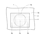
この放熱シート4の平面視(基板2の搭載面2aと対向する側から平面的に見た場合)における外形サイズは、図2に示すように、電子部品1の平面視における外形サイズよりも大きくなっている。なお、放熱シート4の平面視における外形サイズとしては、電子部品1の平面視における外形サイズと同じになっていてもよいし、電子部品1の平面視における外形サイズよりも小さくなっていてもよい。
また、放熱シート4の平面視(基板2の搭載面2aと対向する側から平面的に見た場合)における外形形状は、四角形状とされている。ただし、この外形形状にする必要は特になく、四角形状以外の形状(たとえば、円形状など)になっていてもよい。
ここで、第1実施形態では、図1および図2に示すように、平面視(基板2の搭載面2aと対向する側から平面的に見た場合)において電子部品1の中央部分と重畳することになる放熱シート4の所定部分4aが他の部分(端部)4bよりも電子部品1側に向かって突出している。なお、平面視における電子部品1の中央部分とは、平面視における電子部品1の縁部分よりも内側の部分であり、平面視における電子部品1の縁部分の面積よりも大きい面積を有する部分である。
放熱シート4の所定部分4aを電子部品1側に向かって突出させる方法としては種々あるが、第1実施形態では、電子部品1側に向かって突出する突出部3aを基板カバー3の一部分に設け、その基板カバー3の所定面(基板2の搭載面2aと対向する面)に放熱シート4を貼付することによって、放熱シート4の所定部分4aを電子部品1側に向かって突出させている。
具体的に言うと、第1実施形態では、電子部品1側に向かって突出する突出部3aが基板カバー3の一部分に設けられている一方で、基板カバー3の突出部3aが設けられた部分以外の部分3bについては平坦になっている。また、少なくとも一方向(基板2の搭載面2aに対して平行な方向)においては、基板カバー3の突出部3aの幅W1よりも放熱シート4の幅W2の方が大きくされている。そして、基板カバー3の突出部3aと放熱シート4の所定部分4aとが重畳し、かつ、基板カバー3の平坦な部分3bと放熱シート4の他の部分(端部)4bとが重畳するように、基板カバー3の所定面(基板2の搭載面2aと対向する面)に放熱シート4が貼付されている。
このようになっていると、放熱シート4の形状が基板カバー3の所定面の凹凸形状を略反映した形状となる。すなわち、放熱シート4の所定部分4aが電子部品1側に向かって凸となるように撓む。これにより、放熱シート4の所定部分4aが他の部分(端部)4bよりも電子部品1側に向かって突出した状態となる。
ところで、基板カバー3の突出部3aは、基板カバー3の一部分を電子部品1側に向かって凹ます(突出させる)ことで得られるドーム形状の凹部(凸部)からなっている。このことから、基板カバー3の突出部3aは、基板カバー3の一部分に後付けされたものではなく、基板カバー3の一部分に一体的に形成されたものであることは明らかである。なお、基板カバー3の一部分を電子部品1側に向かって凹ます(突出させる)場合には、基板カバー3の一部分に対してエンボス加工などを施せばよい。
また、この基板カバー3の突出部3aの断面形状としては、半円形状としてもよいが、基板カバー3の所定面(基板2の搭載面2aと対向する面)に貼付した放熱シート4の所定部分4aを電子部品1側に向かって突出させることができるのであれば、半円形状とは異なる形状であってもよい。また、基板カバー3の突出部3aの平面視(基板2の搭載面2aと対向する側から平面的に見た場合)における形状についても特に限定されるものではなく、円形状になっていてもよいし、四角形状になっていてもよいし、それら以外の形状になっていてもよい。
そして、第1実施形態では、放熱シート4の所定部分4aが他の部分(端部)4bよりも電子部品1側に向かって突出した状態で、放熱シート4が電子部品1に対して接触(当接)している。このため、平面視(基板2の搭載面2aと対向する側から平面的に見た場合)における電子部品1の中央部分と放熱シート4との間の接触圧は、平面視における電子部品1の縁部分と放熱シート4との間の接触圧よりも高くなっている。
第1実施形態では、上記のように、平面視(基板2の搭載面2aと対向する側から平面的に見た場合)において電子部品1の中央部分と重畳することになる放熱シート4の所定部分4aを他の部分(端部)4bよりも電子部品1側に向かって突出させ、放熱シート4の所定部分4aが他の部分(端部)4bよりも電子部品1側に向かって突出した状態で、放熱シート4を電子部品1に対して接触させることによって、平面視における電子部品1の縁部分に対する放熱シート4の接触圧が低くなる(あるいは、平面視における電子部品1の縁部分に対して放熱シート4が接触しなくなる)一方で、平面視における電子部品1の中央部分に対する放熱シート4の接触圧は高くなる。すなわち、放熱シート4と電子部品1との間において高い接触圧で確実に接触する面積が増大する。その結果、電子部品1で発生した熱が放熱シート4に伝わり易くなるので、電子部品1で発生した熱を良好に放熱することが可能となる。
また、第1実施形態では、上記のように、放熱シート4の所定部分4aを電子部品1側に向かって凸となるように撓ませることによって、放熱シート4の所定部分4aに突出部が形成されていなかったとしても、容易に、放熱シート4の所定部分4aを電子部品1側に向かって突出させることができる。
また、第1実施形態では、上記のように、電子部品1側に向かって突出する突出部3aを基板カバー3の一部分に設け、さらに、基板カバー3の突出部3aと放熱シート4の所定部分4aとが重畳し、かつ、基板カバー3の平坦な部分3bと放熱シート4の他の部分(端部)4bとが重畳するように、基板カバー3の所定面(基板2の搭載面2aと対向する面)に放熱シート4を貼付することによって、放熱シート4の所定部分4aを電子部品1側に向かって凸となるように撓ませることができる。すなわち、放熱シート4の所定部分4aを電子部品1側に向かって突出させるのが容易となる。
また、第1実施形態では、上記のように、基板カバー3の一部分に電子部品1側に向かって突出する突出部3aを一体的に形成することによって、基板カバー3の一部分に電子部品1側に向かって突出する突出部3aを設けたとしても、部品点数は増加しない。
また、第1実施形態では、上記のように、基板カバー3の一部分を電子部品1側に向かって凹ます(突出させる)ことによって、容易に、電子部品1側に向かって突出する突出部3aを基板カバー3の一部分に一体的に形成することができる。
なお、第1実施形態の変形例としては、以下のようなものが考えられる。
たとえば、第1実施形態では、基板カバー3の突出部3aが1つのドーム形状部からなるようにしたが、図3に示すように、基板カバー3の突出部3aが複数のドーム形状部を連結したもの(波型の突出部)であってもよい。
また、第1実施形態では、基板カバー3の一部分を電子部品1側に向かって凹ますことで基板カバー3の一部分に突出部3aを一体的に形成したが、図4に示すように、基板カバー3の一部分に何らかの熱伝導部材5を後付けし、その後付けされた熱伝導部材5を基板カバー3の突出部3aとして機能させてもよい。すなわち、基板カバー3の突出部3aが基板カバー3とは別部材からなっていてもよい。このように、基板カバー3の一部分に後付けされた熱伝導部材5を基板カバー3の突出部3aとして機能させるようにすると、基板カバー3の一部分に突出部3aを形成するための加工(たとえば、エンボス加工など)が不要となるので、基板カバー3にかかる製造コストを削減することができる。なお、図示しないが、基板カバー3の一部分に複数の熱伝導部材5を後付けし、その複数の熱伝導部材5を基板カバー3の突出部3aとしてもよい。
さらに、基板カバー3の一部分に熱伝導部材5を後付けする場合には、図5に示すように、その熱伝導部材5がヒートパイプであってもよい。このようにすると、放熱特性のより一層の向上を図ることができる。
(第2実施形態)
本発明の第2実施形態による表示装置の構成について、図6~図8を参照して詳細に説明する。
本発明の第2実施形態による表示装置の構成について、図6~図8を参照して詳細に説明する。
この表示装置は、種々の装置(たとえば、テレビ受信装置など)に装着される液晶表示装置であって、図6に示すように、映像を表示する液晶表示パネル31と、液晶表示パネル31の表示面側とは反対の裏面側に設置されるバックライトユニット32とを少なくとも備えている。
液晶表示パネル31は、実際に映像が表示される表示領域と、その表示領域の外縁領域である非表示領域とを有している。そして、液晶表示パネル31の表示領域には、マトリクス状に配列された複数の画素が作り込まれている。
複数の画素のそれぞれは、スイッチング素子、画素電極および共通電極などによって駆動されるようになっている。なお、図面を見易くするため、スイッチング素子、画素電極および共通電極は図示しておらず、それらに対して電気的に接続される配線などについても図示していない。
スイッチング素子はTFT(薄膜トランジスタ)からなっていて、スイッチング素子のゲートはゲート線(走査線)に接続され、スイッチング素子のソースはソース線(データ線)に接続される。また、スイッチング素子のドレインには画素電極が接続されるとともに、その画素電極と対向するように共通電極が配置される。そして、画素電極と共通電極との間に液晶(図示せず)が挟持される。なお、スイッチング素子は各画素に個々に設けられており、画素電極も各画素に個々に設けられている。一方、共通電極については各画素で共通となっている。
表示動作の際には、映像信号に基づいて、液晶表示パネル31の液晶の光学的性質(光透過率)が画素毎に変化される。具体的には、各画素において、スイッチング素子を介して画素電極に所定の電力が供給されることにより、画素電極と共通電極との間に電界が発生される。そして、画素電極と共通電極との間に発生した電界によって、液晶の配向、すなわち、液晶を透過する光の透過率が変化される。
このため、バックライトユニット32からバックライト光が出射され、そのバックライト光によって液晶表示パネル31の裏面が照明されると、液晶表示パネル31を透過するバックライト光の透過量が画素毎に異ならされることになる。これにより、液晶表示パネル31の表示面に所望の映像が表示される。
以下に、液晶表示パネル31の構造についてより詳細に説明する。
液晶表示パネル31は、2枚の透明基板11および12を少なくとも備えている。一方の透明基板11は、アクティブマトリクス基板と称されるものであり、他方の透明基板12は、透明基板11に対して対向配置されることから対向基板と称される場合もあるし、カラーフィルタ基板と称される場合もある。
一方の透明基板11の所定面上には、スイッチング素子および画素電極が形成されているとともに、それらに電気的に接続されるゲート線(走査線)およびソース線(データ線)も形成されている。また、他方の透明基板12の所定面上には、共通電極が形成されている。なお、他方の透明基板12の所定面上には、共通電極に加えて、必要に応じてカラーフィルタがさらに形成される。そして、2枚の透明電極11および12のそれぞれの所定面は、液晶を特定方向に配向させることが可能な配向膜(図示せず)によって覆われている。
また、2枚の透明基板11および12は、それぞれの所定面が向き合うように、シール材(図示せず)を介して互いに貼り合わされている。そして、2枚の透明基板11および12の間に液晶が封止されている。これによって、画素電極と共通電極との間(一方の透明基板11の所定面を覆う配向膜と他方の透明電極12の所定面を覆う配向膜との間)に液晶が挟持された状態となっている。
なお、2枚の透明基板11および12のそれぞれの外形サイズは互いに異なっていて、透明基板11の外形サイズが透明基板12の外形サイズよりも大きくされている。したがって、2枚の透明基板11および12は互いに貼り合わされているが、透明基板11および12のそれぞれの所定端は互いに合致しておらず、透明基板11の所定面の一部が透明基板12から露出されている。この透明基板11の所定面の露出した部分は、非表示領域の一領域であって、透明基板11にドライバ(図示せず)を電気的に接続するために用いられる。
また、これら2枚の透明基板11および12の所定面(液晶側の面)とは反対側の面のそれぞれには、特定の振動方向の光波だけを透過させる偏光シート13が1枚ずつ貼付されている。そして、2枚の偏光シート13のそれぞれの透過軸方向は、互いに約90°ずらされている。
次に、バックライトユニット32の構造について説明する。
次に、バックライトユニット32の構造について説明する。
このバックライトユニット32は、直下型方式を採用したものであって、バックシャーシ21と、反射シート22と、光源23と、光学シート24と、インバータ基板25とを少なくとも備えている。なお、インバータ基板25は、本発明の「基板」の一例である。
バックシャーシ21は、金属板(アルミニウム板や鋼板など)を板金加工したものであって、液晶表示パネル31側が開口するように凹形状に折り曲げられている。すなわち、バックシャーシ21は、底部と、その底部の一方端および他方端にそれぞれ立設された側部とを有していることになる。
反射シート22は、バックシャーシ21の内面に沿って折り曲げられており、バックシャーシ21の底部および側部のそれぞれの内面上に配置されている。すなわち、バックシャーシ21の底部および側部のそれぞれの内面が反射シート22によって覆われている。
光源23は、バックライト光の基となる光を生成するためのものであって、複数の放電管23aを含んでいるとともに、バックシャーシ21の内面(反射シート22で覆われている面)によって囲まれた領域内に配置されている。これにより、光源23で生成された光がバックシャーシ21の内面に向かって進行したとしても、その光は反射シート22によって液晶表示パネル31側に向けて反射されることになる。
光学シート24は、レンズシートや拡散シートなどを含み、バックシャーシ21の開口を液晶表示パネル31側から塞ぐように配置されている。すなわち、この光学シート24によって、光源23が液晶表示パネル31側から覆われていることになる。このため、光源23からの光は、光学シート24に入射することで集光や拡散などが行われた後、液晶表示パネル31の裏面を照明する。
インバータ基板25は、その搭載面25a上にトランスやコンデンサなどの発熱する電子部品26(図7参照)が搭載されたものであって、図示しない配線(コネクタ)などを介して光源23に電気的に接続されている。そして、液晶表示パネル31の裏面に対して照明を行う際には、インバータ基板25から光源23に電力が供給されるようになっている。
このインバータ基板25の保持はバックシャーシ21の底部の外面側で行われており、インバータ基板25の搭載面25aはバックシャーシ21の底部に対して所定の間隔を隔てて対向されている。したがって、インバータ基板25の搭載面25aがバックシャーシ21の底部で覆われ、インバータ基板25の搭載面25a上に搭載された電子部品26(図7参照)もバックシャーシ21の底部で覆われた状態となっている。このことから、第2実施形態では、本発明の「金属板」に相当する部材がバックシャーシ21であると言える。
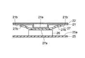
また、図7に示すように、バックシャーシ21の底部と電子部品26との間には、シリコーンゴムシートやアクリルゴムシートなどからなる放熱シート27が配置されている。そして、この放熱シート27は、バックシャーシ21の底部および電子部品26の両方に接触している。このため、電子部品26が発熱すると、その熱が放熱シート27からバックシャーシ21の底部に伝わって放熱される。
ここで、第2実施形態では、図7および図8に示すように、平面視(インバータ基板25の搭載面25aと対向する側から平面的に見た場合)において電子部品26の中央部分と重畳することになる放熱シート27の所定部分27aが他の部分(端部)27bよりも電子部品26側に向かって突出している。そして、放熱シート27の所定部分27aが他の部分(端部)27bよりも電子部品26側に向かって突出した状態で、放熱シート27が電子部品26に対して接触(当接)されている。
なお、第2実施形態では、放熱シート27の所定部分27aを電子部品26側に向かって突出させる方法として、第1実施形態と同様の方法を用いている。
具体的には、バックシャーシ21の底部の一部分を電子部品26側に向かって凹ます(突出させる)ことによって、電子部品26側に向かって突出する突出部21aをバックシャーシ21の底部の一部分に一体的に形成し、バックシャーシ21の底部の突出部21aが形成された部分以外の部分21bについては平坦にしている。そして、バックシャーシ21の底部の突出部21aと放熱シート27の所定部分27aとが重畳し、かつ、バックシャーシ21の底部の平坦な部分21bと放熱シート27の他の部分(端部)27bとが重畳するように、バックシャーシ21の底部の所定面(インバータ基板25の搭載面25aと対向する面)に放熱シート27を貼付している。これにより、放熱シート27の所定部分27aが電子部品26側に向かって凸となるように撓み、放熱シート27の所定部分27aが電子部品26側に向かって突出した状態となる。
ところで、インバータ基板25の搭載面25a上に搭載される電子部品26はトランスなどであるが、平面視(インバータ基板25の搭載面25aと対向する側から平面的に見た場合)におけるトランスの面積(5cm×5cm程度)は比較的大きい。したがって、第2実施形態では、バックシャーシ21の底部の突出部21aの断面形状を隅部に丸みを持たせた四角形状とし、そのバックシャーシ21の底部の突出部21aで放熱シート27の所定部分27aを電子部品26側に向かって突出させることによって、放熱シート27と電子部品26との間の接触面積を大きくとるようにしている。
図6に示した液晶表示パネル31およびバックライトユニット32は、以上のように構成されている。
これら以外の構成部材としては、フレーム33およびフロントベゼル34などがある。フレーム33は、液晶表示パネル31とバックライトユニット32との間に設置されていて、液晶表示パネル31およびバックライトユニット32を保持している。また、フロントベゼル34は、液晶表示パネル31の表示面側に配置されている。そして、フロントベゼル34には開口部が形成されており、そのフロントベゼル34の開口部から液晶表示パネル31の表示面が露出されている。
第2実施形態では、上記のように、電子部品26側に向かって突出する突出部21aをバックシャーシ21の底部の一部分に設け、さらに、バックシャーシ21の底部の突出部21aと放熱シート27の所定部分(平面視において電子部品26の中央部分と重畳することになる部分)27aとが重畳し、かつ、バックシャーシ21の底部の平坦な部分21bと放熱シート27の他の部分(端部)27bとが重畳するように、バックシャーシ21の底部の所定面(インバータ基板25の搭載面25aと対向する面)に放熱シート27を貼付することによって、放熱シート27の所定部分27aが電子部品26側に向かって突出した状態となるので、平面視における電子部品26の中央部分に対する放熱シート27の接触圧が高くなり、放熱シート27と電子部品26との間において高い接触圧で確実に接触する面積が増大する。これにより、第1実施形態と同様、電子部品26で発生した熱が放熱シート27に伝わり易くなるので、電子部品26で発生した熱を良好に放熱することが可能となる。
この第2実施形態のその他の効果は、第1実施形態と同様である。
なお、上記した第2実施形態の変形例としては、第1実施形態の変形例を適用したものが考えられる。
今回開示された実施形態は、すべての点で例示であって制限的なものではないと考えられるべきである。本発明の範囲は、上記した実施形態の説明ではなく特許請求の範囲によって示され、さらに、特許請求の範囲と均等の意味および範囲内でのすべての変更が含まれる。
たとえば、上記第2実施形態では、液晶表示装置に本発明を適用する例について説明したが、本発明はこれに限らず、液晶表示装置以外の表示装置に本発明を適用してもよい。
また、上記第2実施形態では、バックライトユニットを直下型としたが、本発明はこれに限らず、バックライトユニットがエッジライト型であってもよい。
また、上記第2実施形態では、インバータ基板の搭載面をバックシャーシの底部で覆うようにしたが、本発明はこれに限らず、バックシャーシとは異なる金属板を別途準備し、その別途準備した金属板でインバータ基板の搭載面を覆うようにしてもよい。そして、この場合には、インバータ基板の裏面(搭載面とは反対側の面)をバックシャーシの底部と対向させてもよい。
1、26 電子部品
2 基板
2a、25a 搭載面
3 基板カバー(金属板)
3a、21a 突出部
3b、21b 平坦な部分
4、27 放熱シート
4a、27a 所定部分
4b、27b 他の部分
5 熱伝導部材(ヒートパイプ)
21 バックシャーシ(金属板)
25 インバータ基板(基板)
2 基板
2a、25a 搭載面
3 基板カバー(金属板)
3a、21a 突出部
3b、21b 平坦な部分
4、27 放熱シート
4a、27a 所定部分
4b、27b 他の部分
5 熱伝導部材(ヒートパイプ)
21 バックシャーシ(金属板)
25 インバータ基板(基板)
Claims (10)
- 電子部品と、
前記電子部品が搭載される搭載面を有する基板と、
前記電子部品を覆うように前記基板の搭載面と対向して配置される金属板と、
前記金属板と前記電子部品との間に配置される放熱シートとを備え、
前記基板の搭載面と対向する側から平面的に見た場合に前記電子部品の中央部分と重畳することになる前記放熱シートの所定部分が前記放熱シートの他の部分よりも前記電子部品側に向かって突出しており、
前記放熱シートの所定部分が前記放熱シートの他の部分よりも前記電子部品側に向かって突出した状態で、前記放熱シートが前記電子部品に対して接触されていることを特徴とする電子機器。 - 前記放熱シートの所定部分が前記電子部品側に向かって凸となるように撓んでいることにより、前記放熱シートの所定部分が前記電子部品側に向かって突出した状態となっていることを特徴とする請求項1に記載の電子機器。
- 前記金属板の所定面が前記基板の搭載面と対向しており、
前記金属板の所定面に前記放熱シートが貼付されていることを特徴とする請求項2に記載の電子機器。 - 前記金属板の一部分に前記電子部品側に向かって突出する突出部が設けられており、
前記金属板の前記突出部が設けられた部分以外の部分が平坦になっていることを特徴とする請求項3に記載の電子機器。 - 前記突出部が前記金属板の一部分に一体的に形成されたものであることを特徴とする請求項4に記載の電子機器。
- 前記金属板の一部分が前記電子部品側に向かって突出するように凹まされていることにより、前記金属板の一部分に前記突出部が一体的に形成された状態となっていることを特徴とする請求項5に記載の電子機器。
- 前記突出部が前記金属板とは別部材からなっていることを特徴とする請求項4に記載の電子機器。
- 前記突出部が熱伝導部材であることを特徴とする請求項7に記載の電子機器。
- 前記熱伝導部材がヒートパイプであることを特徴とする請求項8に記載の電子機器。
- 請求項1~9のいずれかに記載の電子機器を備えていることを特徴とする表示装置。
Applications Claiming Priority (2)
| Application Number | Priority Date | Filing Date | Title |
|---|---|---|---|
| JP2010161579 | 2010-07-16 | ||
| JP2010-161579 | 2010-07-16 |
Publications (1)
| Publication Number | Publication Date |
|---|---|
| WO2012008398A1 true WO2012008398A1 (ja) | 2012-01-19 |
Family
ID=45469397
Family Applications (1)
| Application Number | Title | Priority Date | Filing Date |
|---|---|---|---|
| PCT/JP2011/065769 Ceased WO2012008398A1 (ja) | 2010-07-16 | 2011-07-11 | 電子機器および表示装置 |
Country Status (1)
| Country | Link |
|---|---|
| WO (1) | WO2012008398A1 (ja) |
Cited By (2)
| Publication number | Priority date | Publication date | Assignee | Title |
|---|---|---|---|---|
| WO2015072315A1 (ja) * | 2013-11-14 | 2015-05-21 | 株式会社フジクラ | 携帯型電子機器の冷却構造 |
| CN117153792A (zh) * | 2018-11-22 | 2023-12-01 | 华为技术有限公司 | 一种封装结构、处理器及服务器 |
Citations (8)
| Publication number | Priority date | Publication date | Assignee | Title |
|---|---|---|---|---|
| JPH0964582A (ja) * | 1995-08-21 | 1997-03-07 | Matsushita Electric Ind Co Ltd | シールドケース構造 |
| JPH1065385A (ja) * | 1996-08-21 | 1998-03-06 | Mitsubishi Electric Corp | 基板ケース構造体 |
| JPH10308484A (ja) * | 1997-05-08 | 1998-11-17 | Casio Comput Co Ltd | 電子機器の放熱構造 |
| JP2002043476A (ja) * | 2000-07-24 | 2002-02-08 | Fujitsu Ten Ltd | 放熱板の構造 |
| JP2002076664A (ja) * | 2000-08-23 | 2002-03-15 | Sony Corp | 放熱装置および放熱装置を有する電子機器 |
| JP2002217343A (ja) * | 2001-01-16 | 2002-08-02 | Denso Corp | 電子装置 |
| JP2005129734A (ja) * | 2003-10-23 | 2005-05-19 | Sony Corp | 電子機器 |
| JP2006099860A (ja) * | 2004-09-29 | 2006-04-13 | Hitachi-Lg Data Storage Inc | 光ディスク装置及び電子機器 |
-
2011
- 2011-07-11 WO PCT/JP2011/065769 patent/WO2012008398A1/ja not_active Ceased
Patent Citations (8)
| Publication number | Priority date | Publication date | Assignee | Title |
|---|---|---|---|---|
| JPH0964582A (ja) * | 1995-08-21 | 1997-03-07 | Matsushita Electric Ind Co Ltd | シールドケース構造 |
| JPH1065385A (ja) * | 1996-08-21 | 1998-03-06 | Mitsubishi Electric Corp | 基板ケース構造体 |
| JPH10308484A (ja) * | 1997-05-08 | 1998-11-17 | Casio Comput Co Ltd | 電子機器の放熱構造 |
| JP2002043476A (ja) * | 2000-07-24 | 2002-02-08 | Fujitsu Ten Ltd | 放熱板の構造 |
| JP2002076664A (ja) * | 2000-08-23 | 2002-03-15 | Sony Corp | 放熱装置および放熱装置を有する電子機器 |
| JP2002217343A (ja) * | 2001-01-16 | 2002-08-02 | Denso Corp | 電子装置 |
| JP2005129734A (ja) * | 2003-10-23 | 2005-05-19 | Sony Corp | 電子機器 |
| JP2006099860A (ja) * | 2004-09-29 | 2006-04-13 | Hitachi-Lg Data Storage Inc | 光ディスク装置及び電子機器 |
Cited By (5)
| Publication number | Priority date | Publication date | Assignee | Title |
|---|---|---|---|---|
| WO2015072315A1 (ja) * | 2013-11-14 | 2015-05-21 | 株式会社フジクラ | 携帯型電子機器の冷却構造 |
| CN105723821A (zh) * | 2013-11-14 | 2016-06-29 | 株式会社藤仓 | 便携式电子设备的冷却构造 |
| CN105723821B (zh) * | 2013-11-14 | 2018-01-02 | 株式会社藤仓 | 便携式电子设备的冷却构造 |
| US10429907B2 (en) | 2013-11-14 | 2019-10-01 | Fujikura Ltd. | Cooling structure for portable electronic device |
| CN117153792A (zh) * | 2018-11-22 | 2023-12-01 | 华为技术有限公司 | 一种封装结构、处理器及服务器 |
Similar Documents
| Publication | Publication Date | Title |
|---|---|---|
| US9939672B2 (en) | Electronic device with heat spreading film | |
| TWI241436B (en) | Liquid crystal display | |
| CN102981329B (zh) | 显示装置 | |
| US8885350B2 (en) | Display device and television receiver | |
| JP2008026866A (ja) | 表示装置 | |
| US9170365B2 (en) | Illumination apparatus, display apparatus, and electronic device | |
| TW201040619A (en) | Protective plate integrated display apparatus | |
| WO2014021209A1 (ja) | 照明装置、表示装置、及びテレビ受信装置 | |
| JP2004212930A (ja) | 液晶表示装置及びその製造方法 | |
| KR20150066312A (ko) | 표시 장치 | |
| JP2012137672A (ja) | 電子機器 | |
| JP2020027190A (ja) | 表示装置 | |
| WO2012035894A1 (ja) | 表示装置、液晶表示装置、および、テレビジョン受信機 | |
| US20180188446A1 (en) | Liquid crystal display | |
| JP2014238578A (ja) | 表示装置 | |
| TWI643002B (zh) | 液晶顯示裝置 | |
| KR102039363B1 (ko) | 액정표시소자 | |
| JP2013218055A (ja) | 表示装置、及びテレビ受信装置 | |
| WO2012008398A1 (ja) | 電子機器および表示装置 | |
| WO2014141882A1 (ja) | 表示装置、及びテレビ受信装置 | |
| JP6529354B2 (ja) | 光源装置および表示装置 | |
| JP2006195296A (ja) | 液晶表示装置 | |
| KR102047223B1 (ko) | 엘이디를 사용하는 백라이트유닛 및 이를 포함하는 액정표시장치 | |
| JP5721660B2 (ja) | 表示装置、及びテレビ受信装置 | |
| KR20170136136A (ko) | 디스플레이 장치 |
Legal Events
| Date | Code | Title | Description |
|---|---|---|---|
| 121 | Ep: the epo has been informed by wipo that ep was designated in this application |
Ref document number: 11806728 Country of ref document: EP Kind code of ref document: A1 |
|
| NENP | Non-entry into the national phase |
Ref country code: DE |
|
| 122 | Ep: pct application non-entry in european phase |
Ref document number: 11806728 Country of ref document: EP Kind code of ref document: A1 |
|
| NENP | Non-entry into the national phase |
Ref country code: JP |