WO2012005292A1 - 半導体基板のエッチング方法および静電容量型memsセンサの製造方法 - Google Patents
半導体基板のエッチング方法および静電容量型memsセンサの製造方法 Download PDFInfo
- Publication number
- WO2012005292A1 WO2012005292A1 PCT/JP2011/065481 JP2011065481W WO2012005292A1 WO 2012005292 A1 WO2012005292 A1 WO 2012005292A1 JP 2011065481 W JP2011065481 W JP 2011065481W WO 2012005292 A1 WO2012005292 A1 WO 2012005292A1
- Authority
- WO
- WIPO (PCT)
- Prior art keywords
- electrode
- semiconductor substrate
- etching
- region
- movable electrode
- Prior art date
- Legal status (The legal status is an assumption and is not a legal conclusion. Google has not performed a legal analysis and makes no representation as to the accuracy of the status listed.)
- Ceased
Links
Images































Classifications
-
- G—PHYSICS
- G01—MEASURING; TESTING
- G01C—MEASURING DISTANCES, LEVELS OR BEARINGS; SURVEYING; NAVIGATION; GYROSCOPIC INSTRUMENTS; PHOTOGRAMMETRY OR VIDEOGRAMMETRY
- G01C19/00—Gyroscopes; Turn-sensitive devices using vibrating masses; Turn-sensitive devices without moving masses; Measuring angular rate using gyroscopic effects
- G01C19/56—Turn-sensitive devices using vibrating masses, e.g. vibratory angular rate sensors based on Coriolis forces
- G01C19/5719—Turn-sensitive devices using vibrating masses, e.g. vibratory angular rate sensors based on Coriolis forces using planar vibrating masses driven in a translation vibration along an axis
- G01C19/5733—Structural details or topology
-
- B—PERFORMING OPERATIONS; TRANSPORTING
- B81—MICROSTRUCTURAL TECHNOLOGY
- B81C—PROCESSES OR APPARATUS SPECIALLY ADAPTED FOR THE MANUFACTURE OR TREATMENT OF MICROSTRUCTURAL DEVICES OR SYSTEMS
- B81C1/00—Manufacture or treatment of devices or systems in or on a substrate
- B81C1/00015—Manufacture or treatment of devices or systems in or on a substrate for manufacturing microsystems
- B81C1/00134—Manufacture or treatment of devices or systems in or on a substrate for manufacturing microsystems comprising flexible or deformable structures
- B81C1/0015—Cantilevers
-
- G—PHYSICS
- G01—MEASURING; TESTING
- G01C—MEASURING DISTANCES, LEVELS OR BEARINGS; SURVEYING; NAVIGATION; GYROSCOPIC INSTRUMENTS; PHOTOGRAMMETRY OR VIDEOGRAMMETRY
- G01C19/00—Gyroscopes; Turn-sensitive devices using vibrating masses; Turn-sensitive devices without moving masses; Measuring angular rate using gyroscopic effects
- G01C19/56—Turn-sensitive devices using vibrating masses, e.g. vibratory angular rate sensors based on Coriolis forces
- G01C19/5719—Turn-sensitive devices using vibrating masses, e.g. vibratory angular rate sensors based on Coriolis forces using planar vibrating masses driven in a translation vibration along an axis
- G01C19/5769—Manufacturing; Mounting; Housings
-
- B—PERFORMING OPERATIONS; TRANSPORTING
- B81—MICROSTRUCTURAL TECHNOLOGY
- B81C—PROCESSES OR APPARATUS SPECIALLY ADAPTED FOR THE MANUFACTURE OR TREATMENT OF MICROSTRUCTURAL DEVICES OR SYSTEMS
- B81C2201/00—Manufacture or treatment of microstructural devices or systems
- B81C2201/01—Manufacture or treatment of microstructural devices or systems in or on a substrate
- B81C2201/0101—Shaping material; Structuring the bulk substrate or layers on the substrate; Film patterning
- B81C2201/0128—Processes for removing material
- B81C2201/013—Etching
- B81C2201/0132—Dry etching, i.e. plasma etching, barrel etching, reactive ion etching [RIE], sputter etching or ion milling
Definitions
- the present invention relates to a method for etching a semiconductor substrate and a method for manufacturing a capacitive MEMS sensor using the same.
- DIE deep reactive ion etching
- An object of the present invention is to provide a method for etching a semiconductor substrate capable of forming a recess having a precisely controlled depth regardless of the shape or size of the etching region.
- Another object of the present invention is to provide a method for manufacturing a capacitive MEMS sensor capable of manufacturing a pair of electrodes (first electrode and second electrode) for detecting a change in capacitance as designed. Is to provide.
- an etching method of a semiconductor substrate is a method of selectively etching an etching region of a semiconductor substrate in which an etching region is defined, and a predetermined number of points from a plurality of locations in the etching region are predetermined.
- Forming a plurality of first recesses having openings of the same shape and size in the etching region by deep reactive ion etching in a pattern; and sidewalls of the semiconductor substrate defining the plurality of first recesses Forming a second recess in which the plurality of first recesses are integrated in the etching region by removing isotropic ion etching.
- the second recess is formed in the etching region defined in the semiconductor substrate.
- the semiconductor substrate Prior to the formation of the second recess, the semiconductor substrate is deeply reactive ion etched in a predetermined pattern from a plurality of locations in the etching region. That is, the deep reactive ion etching is performed on the semiconductor in the etching region with the same pattern (opening pattern having the same shape and size). Therefore, the etching rate when forming the plurality of first recesses in the etching region can be made substantially equal. As a result, by executing the deep reactive ion etching process, it is possible to form a plurality of first recesses having substantially the same depth in the etching region.
- the etching region of the semiconductor substrate can be selectively etched.
- a plurality of first recesses are formed by performing deep ion reactive ion etching of a semiconductor substrate vertically with a pattern having a uniform shape and size.
- a 2nd recessed part can be formed in the depth as designed. Therefore, the second recess having a precisely controlled depth can be formed in the semiconductor substrate regardless of the shape or size of the etching region.
- the semiconductor substrate is vertically deep-digged with an opening pattern having the same shape and size.
- a plurality of first recesses are simultaneously formed in each of the first and second etching regions by performing the isotropic ion etching, and the semiconductor substrate may be isotropically ion-etched in the lateral direction as the second step.
- etching method can be suitably employ
- Serial form to the etching region may be executed and the step of forming the first and second electrodes at the same time.
- the depth of the second recess can be accurately controlled, so that the first region can be formed in any shape or size that is defined for partitioning the first electrode and the second electrode.
- the electrode and the second electrode can be formed with a thickness as designed (thickness in the thickness direction of the semiconductor substrate).
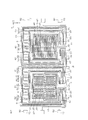
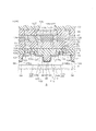
- FIG. 1 is a schematic plan view of a gyro sensor.
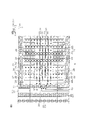
- FIG. 2 is a schematic plan view of the sensor unit shown in FIG.
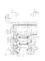
- FIG. 3 is a plan view of an essential part of the X-axis sensor shown in FIG.
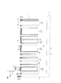
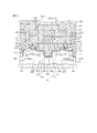
- FIG. 4 is a cross-sectional view of the main part of the X-axis sensor shown in FIG.
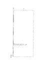
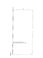
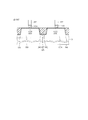
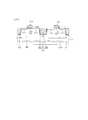
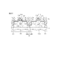
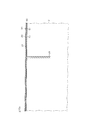
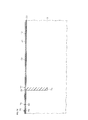
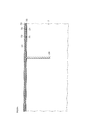
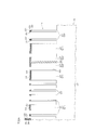
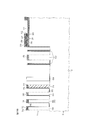
- FIG. 9A is a schematic cross-sectional view showing the manufacturing process of the gyro sensor according to one embodiment of the present invention, and shows a cut surface at the same position as FIG.
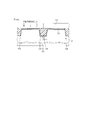
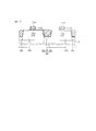
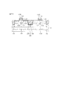
- FIG. 9B is a schematic cross-sectional view showing the manufacturing process of the gyro sensor according to one embodiment of the present invention, and shows a cut surface at the same position as FIG. 6.
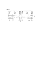
- FIG. 9C is a schematic cross-sectional view showing the manufacturing process of the gyro sensor according to one embodiment of the present invention, and shows a cut surface at the same position as FIG. FIG.
- FIG. 10A is a schematic cross-sectional view showing a step subsequent to FIG. 9A.
- FIG. 10B is a schematic cross-sectional view showing a step subsequent to FIG. 9B.
- FIG. 10C is a schematic cross-sectional view showing a step subsequent to FIG. 9C.
- FIG. 11A is a schematic cross-sectional view showing a step subsequent to FIG. 10A.
- FIG. 11B is a schematic cross-sectional view showing a step subsequent to FIG. 10B.
- FIG. 11C is a schematic cross-sectional view showing a step subsequent to FIG. 10C.
- FIG. 12A is a schematic cross-sectional view showing a step subsequent to FIG. 11A.
- FIG. 12B is a schematic cross-sectional view showing a step subsequent to FIG. 11B.
- FIG. 12C is a schematic cross-sectional view showing a step subsequent to FIG. 11C.
- FIG. 13A is a schematic cross-sectional view showing a step subsequent to FIG. 12A.
- FIG. 13B is a schematic cross-sectional view showing a step subsequent to FIG. 12B.
- FIG. 13C is a schematic cross-sectional view showing a step subsequent to FIG. 12C.
- FIG. 14A is a schematic sectional view showing a step subsequent to FIG. 13A.
- FIG. 14B is a schematic cross-sectional view showing a step subsequent to FIG. 13B.
- FIG. 14C is a schematic cross-sectional view showing a step subsequent to FIG. 13C.
- FIG. 15A is a schematic cross-sectional view showing a step subsequent to FIG. 14A.
- FIG. 15B is a schematic cross-sectional view showing a step subsequent to FIG. 14B.
- FIG. 15C is a schematic cross-sectional view showing a step subsequent to FIG. 14C.
- FIG. 16A is a schematic cross-sectional view showing a step subsequent to FIG. 15A.
- FIG. 16B is a schematic cross-sectional view showing a step subsequent to FIG. 15B.
- FIG. 16C is a schematic cross-sectional view showing a step subsequent to FIG. 15C.
- FIG. 17A is a schematic cross-sectional view showing a step subsequent to FIG. 16A.
- FIG. 17B is a schematic cross-sectional view showing a step subsequent to FIG. 16B.
- FIG. 17C is a schematic cross-sectional view showing a step subsequent to FIG. 16C.
- FIG. 16A is a schematic cross-sectional view showing a step subsequent to FIG. 16A.
- FIG. 17B is a schematic cross-sectional view showing a step subsequent to FIG
- FIG. 18A is a schematic sectional view showing a step subsequent to FIG. 17A.
- FIG. 18B is a schematic cross-sectional view showing a step subsequent to FIG. 17B.
- FIG. 18C is a schematic cross-sectional view showing a step subsequent to FIG. 17C.
- FIG. 19A is a schematic sectional view showing a step subsequent to FIG. 18A.
- FIG. 19B is a schematic cross-sectional view showing a step subsequent to FIG. 18B.
- FIG. 19C is a schematic cross-sectional view showing a step subsequent to FIG. 18C.
- FIG. 20A is a schematic cross-sectional view showing a step subsequent to FIG. 19A.
- FIG. 20B is a schematic cross-sectional view showing a step subsequent to FIG. 19B.
- FIG. 20C is a schematic cross-sectional view showing a step subsequent to FIG. 19C.
- FIG. 21A is a schematic cross-sectional view showing a step subsequent to FIG. 20A.
- FIG. 21B is a schematic cross-sectional view showing a step subsequent to FIG. 20B.
- FIG. 21C is a schematic cross-sectional view showing a step subsequent to FIG. 20C.
- FIG. 22A is a schematic sectional view showing a step subsequent to FIG. 21A.
- FIG. 22B is a schematic cross-sectional view showing a step subsequent to FIG. 21B.
- FIG. 22C is a schematic cross-sectional view showing a step subsequent to FIG. 21C.
- FIG. 23A is a schematic sectional view showing a step subsequent to FIG. 22A.
- FIG. 23B is a schematic cross-sectional view showing a step subsequent to FIG. 22B.
- FIG. 23C is a schematic cross-sectional view showing a step subsequent to FIG. 22C.
- FIG. 24A is a schematic sectional view showing a step subsequent to FIG. 23A.
- FIG. 24B is a schematic sectional view showing a step subsequent to FIG. 23B.
- FIG. 24C is a schematic sectional view showing a step subsequent to FIG. 23C.
- FIG. 25A is a schematic sectional view showing a step subsequent to FIG. 24A.
- FIG. 25B is a schematic sectional view showing a step subsequent to FIG. 24B.
- FIG. 25C is a schematic cross-sectional view showing a step subsequent to FIG. 24C.
- FIG. 24A is a schematic sectional view showing a step subsequent to FIG. 24A.
- FIG. 25B is a schematic sectional view showing a step subsequent to FIG. 24B.
- FIG. 25C is a schematic
- FIG. 26A is a schematic sectional view showing a step subsequent to FIG. 25A.
- FIG. 26B is a schematic cross-sectional view showing a step subsequent to FIG. 25B.
- FIG. 26C is a schematic cross-sectional view showing a step subsequent to FIG. 25C.
- FIG. 27A is a schematic sectional view showing a step subsequent to FIG. 26A.
- FIG. 27B is a schematic cross-sectional view showing a step subsequent to FIG. 26B.
- FIG. 27C is a schematic cross-sectional view showing a step subsequent to FIG. 26C.
- FIG. 28A is a schematic sectional view showing a step subsequent to FIG. 27A.
- FIG. 28B is a schematic cross-sectional view showing a step subsequent to FIG. 27B.
- FIG. 28C is a schematic cross-sectional view showing a step subsequent to FIG. 27C.
- FIG. 29A is a schematic sectional view showing a step subsequent to FIG. 28A.
- FIG. 29B is a schematic sectional view showing a step subsequent to FIG. 28B.
- FIG. 29C is a schematic cross-sectional view showing a step subsequent to FIG. 28C.
- FIG. 30A is a schematic sectional view showing a step subsequent to FIG. 29A.
- FIG. 30B is a schematic sectional view showing a step subsequent to FIG. 29B.
- FIG. 30C is a schematic cross-sectional view showing a step subsequent to FIG. 29C.
- FIG. 31A is a schematic cross-sectional view showing a step subsequent to FIG. 30A.
- FIG. 31B is a schematic cross-sectional view showing a step subsequent to FIG. 30B.
- FIG. 31C is a schematic cross-sectional view showing a step subsequent to FIG. 30C.
- FIG. 32A is a schematic sectional view showing a step subsequent to FIG. 31A.
- FIG. 32B is a schematic cross-sectional view showing a step subsequent to FIG. 31B.
- FIG. 32C is a schematic cross-sectional view showing a step subsequent to FIG. 31C.
- FIG. 33A is a schematic sectional view showing a step subsequent to FIG. 32A.
- FIG. 33B is a schematic cross-sectional view showing a step subsequent to FIG. 32B.
- FIG. 33C is a schematic cross-sectional view showing a step subsequent to FIG. 32C.
- FIG. 32A is a schematic sectional view showing a step subsequent to FIG. 32A.
- FIG. 33B is a schematic cross-sectional view showing a step subsequent to FIG. 32B.
- FIG. 34A is a schematic sectional view showing a step subsequent to FIG. 33A.
- FIG. 34B is a schematic cross-sectional view showing a step subsequent to FIG. 33B.
- FIG. 34C is a schematic cross-sectional view showing a step subsequent to FIG. 33C.
- FIG. 35A is a schematic sectional view showing a step subsequent to FIG. 34A.
- FIG. 35B is a schematic cross-sectional view showing a step subsequent to FIG. 34B.
- FIG. 35C is a schematic cross-sectional view showing a step subsequent to FIG. 34C.
- FIG. 36A is a schematic sectional view showing a step subsequent to FIG. 35A.
- FIG. 36B is a schematic sectional view showing a step subsequent to FIG. 35B.
- FIG. 36C is a schematic cross-sectional view showing a step subsequent to FIG. 35C.
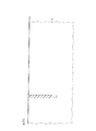
- FIG. 37 is a schematic plan view of the semiconductor substrate in the step of FIG. 31A.
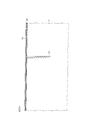
- FIG. 38 is a schematic plan view of the semiconductor substrate in the step of FIG. 31B.
- FIG. 1 is a schematic plan view of a gyro sensor.
- a part of the portion sealed in the resin package is shown in a transparent state.
- the gyro sensor 1 is a capacitance type that is detected based on a change in capacitance of a capacitance element, and includes, for example, camera shake correction of a video camera or a still camera, position detection of a car navigation system, motion detection of a robot or a game machine, etc. Used for applications.
- the gyro sensor 1 has an outer shape of a rectangular parallelepiped-shaped (square shape in plan view) defined by a resin package 2.
- the gyro sensor 1 includes a semiconductor substrate 3 having a rectangular shape in plan view, a sensor unit 4 disposed in the center of the semiconductor substrate 3, and an integrated circuit 5 (ASIC) disposed in the periphery of the semiconductor substrate 3 surrounding the sensor unit 4. : Application Specific Integrated Circuit).
- the sensor unit 4 includes an X-axis sensor 6, a Y-axis sensor 7, and a Z-axis sensor 8 as sensors for detecting angular velocities around three axes that are orthogonal in a three-dimensional space.
- the X-axis sensor 6 uses the vibration Ux in the X-axis direction to generate a Coriolis force Fz in the Z-axis direction when the gyro sensor 1 is tilted, and detects a change in capacitance due to the Coriolis force.
- the angular velocity ⁇ y acting around the Y axis is detected.
- the Y-axis sensor 7 uses the vibration Uy in the Y-axis direction to generate a Coriolis force Fx in the X-axis direction when the gyro sensor 1 is tilted, and detects a change in capacitance due to the Coriolis force.
- the angular velocity ⁇ z acting around the Z axis is detected.
- the Z-axis sensor 8 uses the vibration Uz in the Z-axis direction to generate a Coriolis force Fy in the Y-axis direction when the gyro sensor 1 is tilted, and detects a change in capacitance due to the Coriolis force. Thus, the angular velocity ⁇ x acting around the X axis is detected.
- the integrated circuit 5 performs, for example, a charge amplifier that amplifies the electric signal output from each sensor, a filter circuit (low-pass filter: LPF, etc.) that extracts a specific frequency component of the electric signal, and performs a logical operation on the filtered electric signal.
- a logic circuit is included, and is constituted by, for example, a CMOS device.
- five electrode pads 9 are provided on the surface of the gyro sensor 1 at each of a pair of edge portions facing each other with the sensor unit 4 interposed therebetween in a plan view. The electrode pads 9 are arranged along the respective edges at equal intervals. These electrode pads 9 include, for example, pads for applying a voltage to the sensor unit 4 and the integrated circuit 5.
- FIG. 2 is a schematic plan view of the sensor unit shown in FIG.
- FIG. 3 is a plan view of an essential part of the X-axis sensor shown in FIG. 4 is a cross-sectional view of a principal part of the X-axis sensor shown in FIG. 2, and is a cross-sectional view taken along a cutting line IV-IV in FIG.
- the semiconductor substrate 3 is made of a conductive silicon substrate (for example, a low resistance substrate having a resistivity of 1 m ⁇ ⁇ m to 30 ⁇ ⁇ m, preferably 5 m ⁇ ⁇ m to 25 m ⁇ ⁇ m).
- the semiconductor substrate 3 has a cavity 10 inside, and an X-axis sensor 6 and a Y-axis sensor 7 are formed on an upper wall 11 (surface portion) of the semiconductor substrate 3 having a top surface that partitions the cavity 10 from the surface side. And the Z-axis sensor 8 is formed. That is, the X-axis sensor 6, the Y-axis sensor 7, and the Z-axis sensor 8 are part of the semiconductor substrate 3 and floated with respect to the bottom wall 12 of the semiconductor substrate 3 having a bottom surface that divides the cavity 10 from the back surface side. It is supported by.
- a part of wiring included in these sensors is exposed as a pad 13 on both sides opposed to each other with the cavity 10 interposed therebetween.
- These pads 13 are electrically connected to the electrode pads 9 by, for example, bonding wires (not shown) when packaged by the resin package 2.
- the X-axis sensor 6 and the Y-axis sensor 7 are disposed adjacent to each other with a space therebetween, and the Z-axis sensor 8 is disposed so as to surround each of the X-axis sensor 6 and the Y-axis sensor 7.
- the Y-axis sensor 7 has substantially the same configuration as that obtained by rotating the X-axis sensor 6 by 90 ° in plan view. Therefore, in the following, the configuration of the Y-axis sensor 7 will be replaced with a specific description by describing the portions corresponding to the respective portions in parentheses when describing the respective portions of the X-axis sensor 6.
- a support portion 14 is formed between the X-axis sensor 6 and the Z-axis sensor 8 and between the Y-axis sensor 7 and the Z-axis sensor 8 for supporting them in a floating state.
- the support portion 14 extends from one side wall 15 having a side surface that divides the cavity 10 of the semiconductor substrate 3 from the lateral side, extends across the Z-axis sensor 8 toward the X-axis sensor 6 and the Y-axis sensor 7, and
- An annular portion 17 surrounding the X-axis sensor 6 and the Y-axis sensor 7 is integrally included.
- the X-axis sensor 6 and the Y-axis sensor 7 are arranged inside the individual annular portions 17 and are supported at two opposite positions on the inner wall of the annular portion 17.
- the Z-axis sensor 8 is supported on both side walls of the linear portion 16.
- the X-axis sensor 6 (Y-axis sensor 7) has an X fixed electrode 21 (Y fixed electrode 41) as a first electrode fixed to the support portion 14 provided in the cavity 10, and the X fixed electrode 21. It has X movable electrode 22 (Y movable electrode 42) as the 2nd electrode held so that vibration is possible.
- the X fixed electrode 21 and the X movable electrode 22 are formed with the same thickness.
- the X fixed electrode 21 (Y fixed electrode 41) is spaced from the base portion 23 (base portion 43 of the Y fixed electrode 41) having a square shape in plan view fixed to the support portion 14, along the inner wall of the base portion 23. And a plurality of sets of electrode portions 24 (electrode portions 44 of the Y fixed electrode 41) arranged in a comb-like shape.
- the X movable electrode 22 (Y movable electrode 42) extends in a direction crossing the electrode portion 24 of the X fixed electrode 21, and both ends of the beam portion 25 (beam of the Y-axis sensor 7) can be expanded and contracted along the direction.
- the base part 26 (the base part 46 of the Y movable electrode 42) connected to the base part 23 of the X fixed electrode 21 via the part 45), and the electrode part 24 of the X fixed electrode 21 adjacent to each other from the base part 26. It includes an electrode part 27 (electrode part 47 of the Y movable electrode 42) arranged in a comb-teeth shape that extends to both sides and meshes so as not to contact the electrode part 24 of the X fixed electrode 21.
- the beam portion 25 expands and contracts and the base portion 26 of the X movable electrode 22 vibrates (vibrates Ux) along the surface of the semiconductor substrate 3, so that the electrode portion 24 of the X fixed electrode 21 has comb teeth.
- the base portion 23 of the X fixed electrode 21 has a linear main frame extending in parallel with each other, and a reinforcing frame is combined with the main frame so that a triangular space is repeated along the main frame. It has a truss-like frame structure.
- the electrode portions 24 of the X fixed electrode 21 are equal to each other, with each base end portion connected to the base portion 23 and a pair of two electrode portions in a straight line in plan view whose front ends face each other. A plurality are provided at intervals.
- Each electrode part 24 has a frame structure in a ladder shape in plan view including a linear main frame extending in parallel with each other and a plurality of horizontal frames constructed between the main frames.
- the base portion 26 of the X movable electrode 22 includes a plurality of (six in this embodiment) linear frames extending in parallel with each other, and both ends thereof are connected to the beam portion 25.
- Two beam portions 25 are provided at both ends of the base portion 26 of the X movable electrode 22.
- the electrode portion 27 of the X movable electrode 22 is a planar view ladder including a linear main frame extending in parallel with each other across each frame of the base portion 26 and a plurality of horizontal frames constructed between the main frames. It has a frame structure.
- the insulating layer 28 that crosses the horizontal frame from the surface to the cavity 10 on a line that divides each electrode portion 27 into two along the direction orthogonal to the vibration direction Ux (this implementation) In the form, silicon oxide) is embedded.
- each electrode part 27 is insulated and separated into two on one side and the other side along the vibration direction Ux.
- the separated electrode portions 27 of the X movable electrode 22 function as independent electrodes in the X movable electrode 22.
- a first insulating film 33 and a second insulating film 34 made of silicon oxide (SiO 2 ) are sequentially stacked on the surface of the semiconductor substrate 3 including the X fixed electrode 21 and the X movable electrode 22, and this second insulating film
- An X first drive / detection line 29 (Y first drive / detection line 49) and an X second drive / detection line 30 (Y second drive / detection line 50) are formed on the line 34.
- the X first drive / detection wiring 29 supplies a drive voltage to one side (in this embodiment, the left side in FIG. 3) of each electrode part 27 insulated and separated from the two, and from the electrode part 27 A change in voltage associated with a change in capacitance is detected.
- the X second drive / detection wiring 30 supplies a drive voltage to the other side (in this embodiment, the right side of FIG. 3) of each electrode part 27 that is insulated and separated into two, A change in voltage accompanying a change in capacitance is detected from the electrode unit 27.
- the X first and second drive / detection wirings 29 and 30 are made of aluminum (Al).
- the first and second drive / detection wirings 29 and 30 are electrically connected to the individual electrode portions 27 via contact plugs 31 and 51 penetrating the first and second insulating films 33 and 34.
- the X first and X second drive / detection wires 29 and 30 are routed on the support portion 14 via the beam portion 25 of the X movable electrode 22 and the base portion 23 of the X fixed electrode 21, and a part thereof Is exposed as a pad 13.
- the X first and X second drive / detection wirings 29 and 30 each have a beam portion 25 itself made of a part of the conductive semiconductor substrate 3 in a section passing through the beam portion 25 of the X movable electrode 22. It is used as a current path. Since no aluminum wiring is provided on the beam portion 25, the stretchability of the beam portion 25 can be maintained.
- an X third drive / detection wiring 32 for detecting a change in voltage accompanying a change in capacitance is routed from the electrode portion 24 of the X fixed electrode 21 to the support portion 14, and this X third drive As with the other wirings 29 and 30, a part of the / detecting wiring 32 is exposed as the pad 13.
- the upper surfaces and side surfaces of the X fixed electrode 21 and the X movable electrode 22 are covered with a protective thin film 35 made of silicon oxide (SiO 2 ) together with the first insulating film 33 and the second insulating film 34.
- a third insulating film 36, a fourth insulating film 37, a fifth insulating film 38, and a surface protective film 39 are sequentially stacked on the second insulating film 34 in a portion outside the cavity 10 on the surface of the semiconductor substrate 3. Yes. That is, in this gyro sensor 1, the number of insulating films stacked on the sensor is smaller than the number of insulating films included in the integrated circuit 5, and in this embodiment, the insulating film of the sensor is the first.
- the insulating film 33 has a two-layer structure of a first insulating film 33 and a second insulating film 34, and the insulating film of the integrated circuit 5 has a six-layer structure of first to fifth insulating films 33, 34, 36 to 38 and a surface protective film 39.
- the same polarity / different polarity drive is provided between the X fixed electrode 21 and the X movable electrode 22 via the X first to X third drive / detection wirings 29, 30, 32. Voltage is applied alternately. As a result, Coulomb repulsive force / Coulomb attractive force is alternately generated between the electrode portion 24 of the X fixed electrode 21 and the electrode portion 27 of the X movable electrode 22. As a result, the comb-shaped X movable electrode 22 vibrates left and right (vibrates Ux) along the X-axis direction with respect to the comb-shaped X fixed electrode 21.
- the angular velocity ⁇ y about the Y-axis is obtained by taking a difference between detection values of one and the other electrode portions of the X movable electrode 22 that is insulated and separated.
- the same / different polarity drive voltage is applied between the Y fixed electrode 41 and the Y movable electrode 42 via the Y first to Y third drive / detection wirings 49, 50, 52. Given alternately. As a result, Coulomb repulsive force / Coulomb attractive force is alternately generated between the electrode portion 44 of the Y fixed electrode 41 and the electrode portion 47 of the Y movable electrode 42.
- the comb-shaped Y movable electrode 42 vibrates left and right (vibrates Uy) along the Y-axis direction with respect to the comb-shaped Y fixed electrode 41.
- a Coriolis force Fx is generated in the X axis direction. Due to the Coriolis force Fx, the facing area between the electrode portion 44 of the Y fixed electrode 41 and the electrode portion 47 of the Y movable electrode 42 that are adjacent to each other changes.
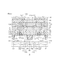
- FIG. 5 is a plan view of the main part of the Z-axis sensor shown in FIG. 6 is a cross-sectional view of a principal part of the Z-axis sensor shown in FIG. 2, and is a cross-sectional view taken along a cutting line VI-VI in FIG. 7 is a cross-sectional view of a principal part of the Z-axis sensor shown in FIG. 2, and is a cross-sectional view taken along the cutting line VII-VII in FIG.
- the semiconductor substrate 3 made of conductive silicon has a cavity 10 inside as described above.
- the upper surface 11 (surface portion) of the semiconductor substrate 3 is supported by the support portion 14 so as to float with respect to the bottom wall 12 of the semiconductor substrate 3 so as to surround each of the X-axis sensor 6 and the Y-axis sensor 7.
- a Z-axis sensor 8 is disposed.
- the Z-axis sensor 8 includes a Z-fixed electrode 61 as a first electrode fixed to a support portion 14 (straight line portion 16) provided in the cavity 10, and a Z-axis sensor 8 that is held so as to be able to vibrate with respect to the Z-fixed electrode 61. And a Z movable electrode 62 as two electrodes.
- the Z fixed electrode 61 and the Z movable electrode 62 are formed with the same thickness.
- the Z movable electrode 62 is disposed so as to surround the annular portion 17 of the support portion 14, and the Z fixed electrode 61 is disposed so as to further surround the Z movable electrode 62.
- the Z fixed electrode 61 and the Z movable electrode 62 are integrally connected to both side walls of the linear portion 16 of the support portion 14.
- the Z fixed electrode 61 includes a base portion 63 as a first base portion having a square ring shape in plan view fixed to the support portion 14, and a linear portion of the base portion 63 with respect to the X axis sensor 6 (Y axis sensor 7).
- 16 includes a plurality of comb-like electrode portions 64 as first electrode portions provided on a portion on the opposite side to 16.
- the Z movable electrode 62 faces the base portion 65 as a second base portion having a square ring shape in plan view and between the base portion 65 and each of the comb-like electrode portions 64 of the Z fixed electrode 61 adjacent to each other.
- an electrode portion 66 as a comb-like second electrode portion that meshes so as not to contact the electrode portion 64 of the Z fixed electrode 61.
- the base portion 65 of the Z movable electrode 62 has a linear main frame extending in parallel with each other, and the reinforcing frame is combined with the main frame so that a triangular space is repeated along the main frame. It has a truss-like frame structure.
- the base portion 65 of the Z movable electrode 62 having such a structure has a section in which the reinforcing frame is omitted in a portion opposite to the side where the electrode section 66 is disposed, and the main frame of the section is the Z frame. It functions as a beam portion 67 for enabling the movable electrode 62 to move up and down.
- the beam portion 67 is distorted, and the base portion 65 of the Z movable electrode 62 is moved toward and away from the cavity 10 with the beam portion 67 as a fulcrum as if it were a pendulum.
- the electrode portion 66 of the Z movable electrode 62 meshed with the electrode portion 64 of the Z fixed electrode 61 in a comb shape vibrates up and down.
- the base portion 63 of the Z fixed electrode 61 has a linear main frame extending in parallel with each other, and a reinforcing frame is combined with the main frame so that a triangular space is repeated along the main frame. It has a truss-like frame structure.
- the individual electrode portions 64 of the Z fixed electrode 61 have base ends connected to the base portion 63 of the Z fixed electrode 61, distal ends extending toward the Z movable electrode 62, and equal intervals along the inner wall of the base portion. They are arranged in a comb shape.
- an insulating layer 68 (silicon oxide in this embodiment) is embedded from the surface to the cavity 10 so as to cross the electrode portion 64 in the width direction in a portion near the base end portion of each electrode portion 64. It is. With this insulating layer 68, the individual electrode portions 64 of the Z fixed electrode 61 are insulated from the other portions of the Z fixed electrode 61.
- the main frame of the truss structure is arranged in the width direction
- An insulating layer 69 as a first isolation insulating layer is embedded from the surface of the semiconductor substrate 3 to the cavity 10 so as to cross.
- each electrode portion 66 of the Z movable electrode 62 has a base end portion 71 connected to the base portion 65 of the Z movable electrode 62 and a distal end portion 70 extending between the electrode portions 64 of the Z fixed electrode 61.
- the Z fixed electrodes 61 are arranged in a comb-teeth shape so as not to contact the electrode portion 64.
- a portion of the Z movable electrode 62 near the tip 70 is provided as a second isolation insulating layer from the surface of the semiconductor substrate 3 to the cavity 10 so as to cross the electrode 66 in the width direction. Insulating layer 73 (in this embodiment, silicon oxide) is embedded.
- the insulating layer 74 (this layer) extends from the surface of the semiconductor substrate 3 to the cavity 10 so as to cross the electrode portion 66 in the width direction.
- silicon oxide is embedded.
- the individual electrode portions 66 of the Z movable electrode 62 are warped in an arc shape in cross section in a direction away from the cavity 10 of the semiconductor substrate 3 so as to protrude from the surface of the electrode portion 64 of the Z fixed electrode 61.
- the first insulating film 33 and the second insulating film 34 made of silicon oxide (SiO 2 ) are sequentially stacked on the surface of the semiconductor substrate 3 including the Z fixed electrode 61 and the Z movable electrode 62.
- the first insulating film 33 is thicker than the other parts on the surface of the Z movable electrode 62.
- a Z first detection wiring 75, a Z first drive wiring 76, a Z second detection wiring 77, and a Z second drive wiring 78 are formed on the second insulating film 34.
- the Z first detection wiring 75 and the Z second detection wiring 77 are respectively connected to the electrode portion 64 of the Z fixed electrode 61 and the intermediate portion 72 of the Z movable electrode 62 which are adjacent to each other. That is, in the Z-axis sensor 8, the electrode portion 64 of the Z fixed electrode 61 and the intermediate portion 72 of the Z movable electrode 62, to which the Z first detection wiring 75 and the Z second detection wiring 77 are connected, are connected to each other.
- the electrodes of the capacitive element (detection unit) are opposed to each other with a distance d, a constant voltage is applied between them, and the capacitance changes according to the change of the distance d.
- the Z first detection wiring 75 is formed along the base portion 63 of the Z fixed electrode 61, and straddles the insulating layer 68 of each electrode portion 64 of the Z fixed electrode 61. It contains aluminum wiring that branches off. The branched aluminum wiring is electrically connected to the front end side of the insulating layer 68 in each electrode part 64 through a contact plug 79 penetrating the first insulating film 33 and the second insulating film 34. .
- the Z first detection wiring 75 is routed on the support portion 14 via the base portion 63 of the Z fixed electrode 61, and a part thereof is exposed as the pad 13.
- the Z second detection wiring 77 detects a change in voltage accompanying a change in capacitance from the electrode portion 66 of the Z movable electrode 62.
- the Z second detection wiring 77 is formed along the base portion 65 of the Z movable electrode 62 and extends to the intermediate portion 72 across the insulating layer 74 near the base end portion 71 of each electrode portion 66 of the Z movable electrode 62. It contains aluminum wiring that branches off.
- the branched aluminum wiring is electrically connected to the intermediate part 72 of each electrode part 66 through a contact plug 80 penetrating the first insulating film 33 and the second insulating film 34.
- the Z second detection wiring 77 is routed on the support portion 14 via the base portion 65 of the Z movable electrode 62, and a part thereof is exposed as the pad 13.
- the Z first drive wiring 76 and the Z second drive wiring 78 are a facing portion 84 (first contact portion) of the Z fixed electrode 61 and a Z movable electrode facing each other in a direction orthogonal to the facing direction of the electrodes constituting the capacitive element. 62 are respectively connected to the distal end portion 70 (second contact portion). That is, in this Z-axis sensor 8, a driving voltage is applied between the opposed portion 84 of the Z fixed electrode 61 and the distal end portion 70 of the Z movable electrode 62, and the coulomb generated by the voltage change of the driving voltage.
- the drive part which vibrates Z movable electrode 62 with force is comprised.
- the Z first drive wiring 76 supplies a drive voltage to the facing portion 84 of the Z fixed electrode 61.
- the Z first drive wiring 76 spans both sides of the insulating layer 69 using the surface of the second insulating film 34 and faces the opposing portion 84 via a contact plug 85 penetrating the first insulating film 33 and the second insulating film 34.
- the aluminum wiring electrically connected to the portion excluding the facing portion 84 of the base portion 63, and the remaining portion is configured using the base portion 63 of the Z fixed electrode 61 made of conductive silicon. Yes.
- the Z first drive wiring 76 is routed on the support portion 14, and a part thereof is exposed as the pad 13.
- the Z second drive wiring 78 supplies a drive voltage to the tip portion 70 of the Z movable electrode 62.
- the Z second drive wiring 78 extends between the distal end portion 70 and the proximal end portion 71 of the electrode portion 66 using the surface of the second insulating film 34 and penetrates the first insulating film 33 and the second insulating film 34.
- An aluminum wiring electrically connected to the distal end portion 70 and the proximal end portion 71 through a contact plug 86, and the remaining portion uses the base portion 65 of the Z movable electrode 62 made of conductive silicon. Configured. Further, as shown in FIG. 2, the Z second drive wiring 78 is routed on the support portion 14 and a part thereof is exposed as the pad 13.
- the upper surfaces and side surfaces of the Z fixed electrode 61 and the Z movable electrode 62 are covered with a protective thin film 35 made of silicon oxide (SiO 2 ) together with the first insulating film 33 and the second insulating film 34.
- a third insulating film 36, a fourth insulating film 37, a fifth insulating film 38, and a surface protective film 39 are sequentially stacked on the second insulating film 34 in a portion outside the cavity 10 on the surface of the semiconductor substrate 3. Yes.
- the opening 82 exposing the Z first detection wiring 75, the Z first drive wiring 76, the Z second detection wiring 77, and the Z second drive wiring 78 as the pad 13 is provided on the surface.
- the protective film 39 is formed through the fifth, fourth and third insulating films 36.
- the same polarity / position is provided between the facing portion 84 of the Z fixed electrode 61 and the tip portion 70 of the Z movable electrode 62 via the Z first drive wiring 76 and the Z second drive wiring 78.
- Different polarity driving voltages are applied alternately.
- Coulomb repulsive force / Coulomb attractive force is alternately generated between the facing portion 84 of the Z fixed electrode 61 and the tip portion 70 of the Z movable electrode 62.
- the comb-shaped Z movable electrode 62 is a pendulum
- the comb-shaped Z fixed electrode 61 is also vertically moved along the Z-axis direction with respect to the Z fixed electrode 61 with the vibration center as the center.
- the angular velocity ⁇ x around the X axis is obtained by taking the difference between the detection value of the Z axis sensor 8 surrounding the X axis sensor 6 and the detection value of the Z axis sensor 8 surrounding the Y axis sensor 7. Desired.
- the difference is obtained, for example, by reversing the positional relationship between the fixed electrode and the movable electrode of the Z-axis sensor 8 surrounding the X-axis sensor 6 and the fixed electrode and the movable electrode of the Z-axis sensor 8 surrounding the Y-axis sensor 7. be able to. That is, in one Z-axis sensor 8, as described above, the Z movable electrode 62 is disposed so as to surround the annular portion 17 of the support portion 14, and the Z fixed electrode 61 is disposed so as to further surround the Z movable electrode 62. Deploy.
- a Z fixed electrode is disposed so as to surround the annular portion 17 of the support portion 14, and a Z movable electrode is disposed so as to further surround the Z fixed electrode.
- the Z movable electrode is disposed so as to surround the annular portion 17 of the support portion 14, and the Z fixed electrode is disposed so as to further surround the Z movable electrode. Then, the warp direction of the other Z movable electrode is not the direction away from the cavity 10 but the direction toward the back surface of the semiconductor substrate 3 so that the Z movable electrode protrudes from the back surface of the Z fixed electrode.
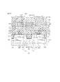
- FIG. 8 is a schematic cross-sectional view of the integrated circuit shown in FIG. 8 is different in scale from the above-described other cross-sectional views (FIGS. 4, 6, and 7), and therefore the size of the expression is different even in the portion to which the same reference numerals are assigned. .
- the integrated circuit 5 is formed on the semiconductor substrate 3 on which the X-axis sensor 6, the Y-axis sensor 7, and the Z-axis sensor 8 are formed so as to surround them.
- the integrated circuit 5 is composed of a CMOS device, and includes an N channel MOSFET 91 and a P channel MOSFET 92 formed on the semiconductor substrate 3.
- the NMOS region 93 in which the N-channel MOSFET 91 is formed and the PMOS region 94 in which the P-channel MOSFET 92 is formed are insulated and isolated from each other by the element isolation unit 95.
- the element isolation portion 95 forms a trench (shallow trench 96) dug relatively shallowly from the surface of the semiconductor substrate 3, forms a thermal oxide film 97 on the inner surface of the shallow trench 96 by a thermal oxidation method, and then performs CVD.
- An insulator 98 for example, silicon oxide (SiO 2 ) is deposited in the shallow trench 96 by the (Chemical Vapor Deposition) method.
- a P-type well 99 is formed in the NMOS region 93.
- the depth of the P-type well 99 is larger than the depth of the shallow trench 96.
- an N-type source region 101 and a drain region 102 are formed in the surface layer portion of the P-type well 99 with the channel region 100 interposed therebetween.
- the end portions of the source region 101 and the drain region 102 on the channel region 100 side have a small depth and impurity concentration. That is, in the N-channel MOSFET 91, an LDD (Lightly Doped Drain) structure is applied.
- LDD Lightly Doped Drain
- a gate insulating film 103 is provided on the channel region 100.
- the gate insulating film 103 is formed in the same layer as the first insulating film 33 (that is, in contact with the surface of the semiconductor substrate 3).
- a gate electrode 104 is provided on the gate insulating film 103.
- the gate electrode 104 is made of N-type polycrystalline silicon (Poly-Si).
- a sidewall 105 is formed around the gate insulating film 103 and the gate electrode 104.
- the sidewall 105 is made of silicon nitride (SiN).
- Silicides 106 to 108 are formed on the surfaces of the source region 101, the drain region 102, and the gate electrode 104, respectively.
- An N-type well 109 is formed in the PMOS region 94. The depth of the N-type well 109 is larger than the depth of the shallow trench 96.
- a P-type source region 111 and a drain region 112 are formed with a channel region 110 interposed therebetween. The depth and impurity concentration of the end portions of the source region 111 and the drain region 112 on the channel region 110 side are reduced. That is, the LD channel structure is applied to the P-channel MOSFET 92.
- a gate insulating film 113 is formed on the channel region 110.
- the gate insulating film 113 is made of silicon oxide.
- a gate electrode 114 is formed on the gate insulating film 113.
- Gate electrode 114 is made of P-type polycrystalline silicon.
- a sidewall 115 is formed around the gate insulating film 113 and the gate electrode 114.
- the sidewall 115 is made of SiN.
- Silicides 116 to 118 are formed on the surfaces of the source region 111, the drain region 112, and the gate electrode 114, respectively.
- second to fifth insulating films 34, 36 to 38 and a surface protective film 39 are sequentially laminated. These insulating films are the same as the second to fifth insulating films 34, 36 to 38 and the surface protective film 39 shown in FIGS.
- Drain wirings 119 and 120 and source wirings 121 and 122 are formed on the lowermost second insulating film 34. These wires are made of aluminum (Al), and are the same as the wires (X first drive / detection wire 29, Z first detection wire 75, etc.) of the X-axis sensor 6, the Y-axis sensor 7, and the Z-axis sensor 8 described above. It is formed in one layer.
- the source lines 121 and 122 are formed above the source region 101 and the source region 111, respectively. Between the source wiring 121 and the source region 101 and between the source wiring 122 and the source region 111, contact plugs 123 and 124 for electrically connecting them penetrate through the second insulating film 34. Is provided.
- the drain wirings 119 and 120 are formed above the drain region 102 and the drain region 112, respectively. Between the drain wiring 119 and the drain region 102 and between the drain wiring 120 and the drain region 112, contact plugs 125 and 126 for electrically connecting them penetrate through the second insulating film 34. Is provided. Similarly, wirings 127 are formed on the third to fifth insulating films 36 to 38, respectively, and the wirings 127 of the insulating films in the respective layers are electrically connected to each other through contact plugs 128. .
- the drain wiring 129 is formed across the drain region 102 and the drain region 112, and the drain wiring 129 includes the drain wiring 119 of the N-channel MOSFET 91 and the drain of the P-channel MOSFET 92.
- the wiring 120 is connected to both.
- the contact plugs 123 to 126, 128 are made of tungsten (W).
- the surface protective film 39 is formed with an opening 130 that exposes a part of the drain wiring 129 formed on the uppermost fifth insulating film 38 as a pad.
- the drain wiring 129 exposed as a pad is electrically connected to the electrode pad 9 by, for example, a bonding wire (not shown) while being packaged by the resin package 2.
- FIG. 9A to FIG. 36A are schematic cross-sectional views showing the manufacturing process of the gyro sensor according to one embodiment of the present invention in the order of steps, and show a cut surface at the same position as FIG.
- FIG. 9B to FIG. 36B are schematic cross-sectional views showing the manufacturing process of the gyro sensor according to one embodiment of the present invention in the order of steps, and show a cut surface at the same position as FIG.
- FIGS. 9C to 36C are schematic cross-sectional views showing the manufacturing process of the gyro sensor according to one embodiment of the present invention in the order of steps, and show a cut surface at the same position as FIG.
- the surface of the semiconductor substrate 3 made of conductive silicon is thermally oxidized (for example, temperature 1100 to 1200 ° C., film thickness 5000 mm). .
- the first insulating film 33 is formed on the surface of the semiconductor substrate 3.
- the oxidation time of the region where the Z movable electrode 62 is to be formed is made longer than the oxidation time of other portions, and the thickness of the region is increased.
- the first insulating film 33 is patterned by a known patterning technique, and the insulating layers 28, 68, 69, 73 and 74 are embedded in the X-axis sensor 6 and the Z-axis sensor 8.
- An opening 18 is formed in the power region.
- the semiconductor substrate 3 is dug down by anisotropic deep RIE (reactive ion etching) using the first insulating film 33 as a hard mask, specifically, by a Bosch process. As a result, a trench 19 is formed in the semiconductor substrate 3.
- anisotropic deep RIE reactive ion etching
- the process of etching the semiconductor substrate 3 using SF 6 (sulfur hexafluoride) and the process of forming a protective film on the etched surface using C 4 F 8 (perfluorocyclobutane) are alternated.
- the semiconductor substrate 3 can be etched with a high aspect ratio, but wavy irregularities called scallops are formed on the etched surface (inner peripheral surface of the trench).
- the region where the integrated circuit 5 is to be formed is maintained as it is after the previous step.
- the inside of the trench 19 and the surface of the semiconductor substrate 3 are thermally oxidized (for example, temperature 1100 to 1200 ° C.), and then the surface of the oxide film is etched back (for example, etched) The film thickness after the back is 21800 mm).
- insulating layers 28, 68, 69, 73, and 74 that fill the trench 19 are formed.
- FIG. 11C the region where the integrated circuit 5 is to be formed is maintained as it is after the previous step.
- the region where the sensor unit 4 is to be formed is divided into the N channel MOSFET 91 and the region where the integrated circuit 5 is to be formed by the steps shown in FIGS. 12C to 23C.
- the P-channel MOSFET 92 is formed, the state after the previous process is maintained (except for the time of etch back in FIG. 17C).
- the first insulating film is formed by CVD as shown in FIG. 12C.
- a silicon nitride film 20 is formed on 33.
- the silicon nitride film 20 and the first insulating film 33 are patterned by a known patterning technique, and an opening 53 is formed in a region where the shallow trench 96 is to be formed.
- the semiconductor substrate 3 is dug down by dry etching using the silicon nitride film 20 and the first insulating film 33 as hard masks. Thereby, a shallow trench 96 is formed in the semiconductor substrate 3.
- the inner surface of the shallow trench 96 is oxidized by thermal oxidation with the silicon nitride film 20 and the first insulating film 33 left. As a result, a thermal oxide film 97 is formed on the inner surface of the shallow trench 96.
- silicon oxide (SiO 2 ) is deposited on the semiconductor substrate 3 by the CVD method, and then etched back. As a result, an insulator 98 that fills the shallow trench 96 is formed. After the formation of the insulator 98, the silicon nitride film 20 is removed.
- a resist 54 having an opening that selectively exposes the PMOS region 94 is formed, and N-type impurities (for example, phosphorus (P) ions) are implanted (in) using the resist 54 as a mask. Plantation).
- N-type impurities for example, phosphorus (P) ions
- a resist 55 having an opening for selectively exposing the NMOS region 93 is formed, and P-type impurities (for example, boron (B) ions) are implanted (in) using the resist 55 as a mask. Plantation). Thereafter, the semiconductor substrate 3 is heat-treated to activate the implanted ions, and the N-type well 109 and the P-type well 99 are formed in the semiconductor substrate 3.
- P-type impurities for example, boron (B) ions
- the first insulating film 33 is thinned by etch back, and the gate insulating films 103 and 113 are formed.
- a polycrystalline silicon layer 56 is formed on the gate insulating films 103 and 113 by the CVD method.
- a resist 57 having an opening is formed in a region other than the region where the gate electrodes 104 and 114 are to be formed, and the polycrystalline silicon layer 56 is etched using the resist 57 as a mask. Thereby, the gate electrodes 104 and 114 are formed. After the formation of the gate electrodes 104 and 114, the resist 57 is removed.
- N-type impurities are implanted into the gate electrode 104 and P-type impurities are implanted into the gate electrode 114 by a known ion implantation technique.
- impurity ions are implanted into the surface layer portions of the NMOS region 93 and the PMOS region 94 at a low concentration.
- a silicon nitride film 58 is formed on the semiconductor substrate 3 by CVD, as shown in FIG. 20C.
- the silicon nitride film 58 is etched back, whereby the sidewalls 105 and 115 are formed simultaneously.
- a resist (not shown) having an opening for selectively exposing the NMOS region 93 is formed on the semiconductor substrate 3, and N is formed on the semiconductor substrate 3 through the opening of the resist. Type impurities are implanted. As a result, an N-type source region 101 and drain region 102 are formed.
- a resist (not shown) having an opening for selectively exposing the PMOS region 94 is formed on the semiconductor substrate 3, and a P-type impurity is implanted into the semiconductor substrate 3 through the opening of the resist. As a result, a P-type source region 111 and drain region 112 are formed.
- the surface layers of the source regions 101 and 111, the drain regions 102 and 112, and the gate electrodes 104 and 114 are silicided, whereby silicides 106 to 108 and 116 to 118 are formed.
- a second insulating film 34 made of silicon oxide is stacked on the semiconductor substrate 3 by the CVD method.
- FIGS. 25A to 25C there are openings in regions where the contact plugs 31, 51, 79, 80, 85, 86 of the sensor unit 4 and the contact plugs 123 to 126, 128 of the integrated circuit 5 are to be formed.
- a resist (not shown) is formed, and the second insulating film 34 and the first insulating film 33 are continuously etched through the opening of the resist. Thereby, a contact hole for burying the contact plug is formed at the same time.
- a tungsten film that fills up the contact hole is deposited by CVD, and the deposited tungsten film is polished by CMP.
- contact plugs 31, 51, 79, 80, 85, 86 of the sensor unit 4 and contact plugs 123 to 126, 128 of the integrated circuit 5 are simultaneously formed of tungsten.
- the third insulating film 36 is laminated on the second insulating film 34 by the CVD method.
- the deposition of the insulating film by CVD, the formation of the contact plug, and the formation of the aluminum wiring are sequentially repeated, and the fourth insulating film 37 and the fifth insulating film 38 are respectively formed.
- a multilayer wiring structure in which the wiring 127 is formed is formed. After the formation of the multilayer wiring structure, a surface protective film 39 is formed.
- the third to fifth insulating films 36 to 38 and the surface protective film 39 on the region where the cavity 10 of the semiconductor substrate 3 is to be formed are removed by etching.
- an opening 82 for exposing the wiring (X first drive / detection wiring 29, Z first detection wiring 75, etc.) of the sensor unit 4 as the pad 13 and the uppermost drain wiring 129 in the integrated circuit 5 are padded.
- An opening 130 is formed as shown in FIG. 30C.
- the semiconductor substrate In the region where the sensor unit 4 is to be formed, after the third to fifth insulating films 36 to 38 and the surface protective film 39 in the region where the cavity 10 is to be formed are removed, the semiconductor substrate according to the embodiment of the present invention.
- the etching method the region where the X fixed electrode 21, the Y fixed electrode 41 and the Z fixed electrode 61, the X movable electrode 22, the Y movable electrode 42 and the Z movable electrode 62 are to be formed in the semiconductor substrate 3 is partitioned.
- the etching region 87 as the first etching region and the second etching region is etched.
- This etching region 87 includes a plurality of portions partitioned independently (for example, a region 871 that partitions the beam portion 25 of the X movable electrode 22, a comb formed by meshing the X fixed electrode 21 and the X movable electrode 22).
- FIG. 31A, FIG. 31B, FIG. 37 (the cut surface along the cutting line AA in FIG. 37 is FIG. 31A) and FIG. 38 (the cut surface along the cutting line BB in FIG. 38).
- a resist 59 is formed on the semiconductor substrate 3.
- the resist 59 has a large number of openings 88 of the same pattern (in this embodiment, circular patterns in plan view having the same shape and size) that face each other for each of the plurality of independent etching regions 87.
- the aperture ratio of the unit area (1 mm 2 ) of the resist 59 is, for example, 1 to 20%.
- the distance D between the centers of the adjacent openings 88 is, for example, 3 ⁇ m to 30 ⁇ m.
- the openings 88 are shown to be large for ease of illustration, but in reality, the openings 88 are sized such as the X fixed electrode 21 and the Z fixed electrode 61. It is very small compared.
- the semiconductor substrate 3 is dug down by anisotropic deep RIE using the resist 59 as a mask, specifically by a Bosch process.
- the etching depth is the same as the thickness of the X fixed electrode 21, the Y fixed electrode 41 and the Z fixed electrode 61, and the X movable electrode 22, the Y movable electrode 42 and the Z movable electrode 62 to be formed.
- a large number of cylindrical recesses 89 as first recesses having substantially the same depth are formed on the surface portion of the semiconductor substrate 3.
- planar outlines of the X fixed electrode 21, the Y fixed electrode 41 and the Z fixed electrode 61, and the X movable electrode 22, the Y movable electrode 42 and the Z movable electrode 62 are formed in the etching region 87.
- the resist 59 is peeled off.
- an etching solution for example, hydrofluoric acid
- etching solution for example, hydrofluoric acid
- the side walls 90 of the semiconductor substrate 3 that define a large number of recesses 89 are removed by etching in the lateral direction parallel to the surface of the semiconductor substrate 3.
- the surface portion of the semiconductor substrate 3 is formed into the shapes of the X fixed electrode 21, the Y fixed electrode 41, and the Z fixed electrode 61, and the X movable electrode 22, the Y movable electrode 42, and the Z movable electrode 62.
- a trench 60 as a second recess is formed therebetween.
- the etching solution supplied to the recess 89 also comes into contact with the portions of the semiconductor substrate 3 that become the respective electrodes (X fixed electrode 21, Z fixed electrode 61, etc.), but compared with the thickness of the portion.
- the width of the side wall 90 that defines the recess 89 is very small.
- the width W 2 (W 1 / W 2 ) of the side wall 90 with respect to the width W 1 along the surface of the semiconductor substrate 3 at the portion that becomes the Z fixed electrode 61 is 10 to 100. Therefore, it is possible to maintain the shape of the portion to be each electrode (X fixed electrode 21, Z fixed electrode 61, etc.) as designed.
- the trench 60 is formed by integrating a large number of cylindrical recesses 89, and the bottom wall of the trench 60 is maintained as the bottom wall of the recesses 89. Therefore, the trench 60 is not flat and actually has undulations. It may be uneven.
- the X fixed electrode 21, the Y fixed electrode 41 and the Z fixed electrode 61, the X movable electrode 22, the Y movable electrode 42 and the Z movable electrode 62 are formed by thermal oxidation or PECVD.
- a protective thin film 35 made of silicon oxide (SiO 2 ) is formed on the entire surface of the substrate and the entire inner surface of the trench 60 (that is, the side surface and the bottom surface defining the trench 60).
- the portion of the protective thin film 35 on the bottom surface of the trench 60 is removed by etch back. As a result, the bottom surface of the trench 60 is exposed.
- the bottom surface of the trench 60 is further dug down by anisotropic deep RIE using the surface protective film 39 as a mask. As a result, an exposed space 83 in which the crystal plane of the semiconductor substrate 3 is exposed is formed at the bottom of the trench 60.
- reactive ions and etching gas are supplied to the exposed space 83 of the trench 60 by isotropic RIE.
- the semiconductor substrate 3 is etched in the direction parallel to the surface of the semiconductor substrate 3 while being etched in the thickness direction of the semiconductor substrate 3 starting from each exposed space 83 by the action of the reactive ions and the like.
- all the exposed spaces 83 adjacent to each other are integrated to form the cavity 10 inside the semiconductor substrate 3, and in the cavity 10, the X fixed electrode 21, the Y fixed electrode 41 and the Z fixed electrode 61,
- the X movable electrode 22, the Y movable electrode 42, and the Z movable electrode 62 are in a floating state.
- the method shown in FIG. 31A, FIG. 31B, FIG. 37 and FIG. 38 is applied.
- a large number of recesses having openings of the same pattern are formed by deep RIE.
- the exposed space 83 may be formed by removing the sidewalls of the recesses by isotropic etching, and then the exposed space 83 may be integrated.
- the depth position of the bottom wall 12 of the semiconductor substrate 3 that divides the cavity 10 from the bottom surface side does not have a particularly bad influence on the operation of the gyro sensor 1 and therefore may not be applied.
- the gyro sensor 1 shown in FIG. 1 is obtained.
- an etching region 87 (for example, a region including regions 871 to 874) for selectively etching the semiconductor substrate 3 is set.
- the semiconductor substrate 3 Prior to the formation of the trench 60 for defining these electrodes, as a first step, as shown in FIGS. 31A, 31B, 37 and 38, the semiconductor substrate 3 is formed in the same pattern (this embodiment). Then, anisotropic deep digging reactive ion etching is performed using as a mask a resist 59 having a large number of openings 88 of the same shape and size (circular pattern in plan view). That is, the semiconductor in the etching region 87 is deep reactive ion etching with the same pattern. Thereby, a large number of recesses 89 having substantially the same depth can be formed on the surface portion of the semiconductor substrate 3.
- the side walls 90 of the semiconductor substrate 3 defining a large number of recesses 89 are etched and removed in the lateral direction parallel to the surface of the semiconductor substrate 3.
- a large number of recesses 89 are integrated, whereby a trench 60 occupying the etching region 87 is formed.
- the etching region 87 of the semiconductor substrate 3 can be selectively etched, and the X fixed electrode 21, the Y fixed electrode 41, the Z fixed electrode 61, the X movable electrode 22, the Y movable electrode 42, and the Z movable electrode 62 can be etched.
- the trench 60 can be formed between them while being formed into a shape.
- the trench 60 is formed as designed by forming the recesses 89 having substantially the same depth by performing deep reactive ion etching of the semiconductor substrate 3 in a pattern having a uniform shape and size. Can be formed at a depth of Therefore, even if the shape and size of the etched region are completely different, such as a very intricate region such as the etching regions 872 and 873 and a simple region such as the etching region 874, it is accurate.
- the trench 60 having a controlled depth can be formed.
- the X fixed electrode 21, the Y fixed electrode 41, the Z fixed electrode 61, the X movable electrode 22, the Y movable electrode 42, and the Z movable electrode 62 which are defined by the trench 60, have a thickness as designed (semiconductor substrate). 3 in the thickness direction).
- the opposing area between the electrode part 24 of the X fixed electrode 21 and the electrode part 27 of the X movable electrode 22, the opposing area between the electrode part 44 of the Y fixed electrode 41 and the electrode part 47 of the Y movable electrode 42, and Z fixation Since the facing area S between the electrode part 64 of the electrode 61 and the intermediate part 72 of the Z movable electrode 62 can be made as designed, the angular velocity of the gyro sensor 1 can be detected well.
- the depth of the trench 60 can be accurately controlled, so that it is formed in the etching region 87. All the trenches 60 can be made to have substantially the same depth. Also, as shown in FIGS. 37 and 38, in the first step of deep RIE, etching is performed with the same pattern from any location on the semiconductor substrate 3 (circular in plan view in this embodiment). Therefore, only one mask is required for patterning the resist 59 formed on the semiconductor substrate 3. Therefore, the manufacturing cost can be reduced. Furthermore, since the resist 59 is patterned once, the manufacturing time can be shortened.
- the capacitive gyro sensor is taken up as an example in which the etching method according to the embodiment of the present invention is adopted.
- the etching method is applied to each axis of the capacitive acceleration sensor.
- the present invention can also be applied when forming a fixed electrode and a movable electrode (X axis, Y axis, and Z axis).
- the present invention can be applied not only to the manufacture of electrodes for capacitance type gyro sensors and acceleration sensors, but also, for example, when forming a recess serving as a reference pressure chamber of a piezoresistive type pressure sensor in a semiconductor substrate, a gate trench of a trench gate type MOSFET.
- the present invention can be applied to all processes for forming a recess in a semiconductor substrate.
- the pattern formed as the first step is a circular shape in plan view as shown in FIGS. 37 and 38.
- an elliptical shape, a square shape, a rectangular shape, and a rhombus shape in plan view are used. , Triangles, trapezoids, etc.
- the mode in which the sensor unit 4 and the integrated circuit 5 are mixedly mounted on the semiconductor substrate 3 has been described.
- the sensor unit 4 and the integrated circuit 5 may be formed on separate semiconductor substrates. Good.
- the aluminum wiring (for example, the X first drive / detection wiring 29, the Z first detection wiring 75, etc.) of the sensor routed on the surface of the semiconductor substrate 3 forms a gate electrode of the integrated circuit 5.
- it can be replaced with wiring made of polysilicon.
- impurities may not be implanted into the polysilicon wiring. This is because the polysilicon wiring is not a wiring for supplying a current to each part of the sensor but a wiring for applying a voltage, and the resistance may be relatively high.
Landscapes
- Engineering & Computer Science (AREA)
- Manufacturing & Machinery (AREA)
- Physics & Mathematics (AREA)
- General Physics & Mathematics (AREA)
- Radar, Positioning & Navigation (AREA)
- Remote Sensing (AREA)
- Microelectronics & Electronic Packaging (AREA)
- Gyroscopes (AREA)
- Pressure Sensors (AREA)
- Drying Of Semiconductors (AREA)
- Micromachines (AREA)
Abstract
本発明の半導体基板のエッチング方法は、エッチング領域が定められた半導体基板の当該エッチング領域を選択的にエッチングする方法であって、当該エッチング領域内の複数箇所から所定のパターンで深掘り反応性イオンエッチングすることにより、同一形状および大きさの開口を有する複数の第1凹部を前記エッチング領域に形成する工程と、複数の前記第1凹部を区画する前記半導体基板の側壁を等方性イオンエッチングで除去することにより、複数の前記第1凹部が一体化された第2凹部を前記エッチング領域に形成する工程とを含む。
Description
本発明は、半導体基板のエッチング方法およびそれを利用した静電容量型MEMSセンサの製造方法に関する。
近年、MEMS(Micro Electro Mechanical Systems)技術を応用したデバイスが携帯電話機などに搭載され始めたことから、MEMSデバイスが注目されている。
MEMSデバイスの作製に際し、高いアスペクト比でエッチングする技術として、深掘り反応性イオンエッチング(深掘りRIE:Deep Reactive Ion Etching)が知られている。
MEMSデバイスの作製に際し、高いアスペクト比でエッチングする技術として、深掘り反応性イオンエッチング(深掘りRIE:Deep Reactive Ion Etching)が知られている。
深掘りRIEは、半導体基板におけるエッチングパターンの形状によって、そのエッチングレートが異なる。そのため、MEMSデバイス作製の際、形状や大きさが異なるエッチングパターンが混在していると、深掘りRIEにより形成された凹部の深さが、パターンごとにばらばらになる。
本発明の目的は、エッチング領域の形状または大きさによらずに、正確に制御された深さの凹部を形成することができる半導体基板のエッチング方法を提供することである。
本発明の目的は、エッチング領域の形状または大きさによらずに、正確に制御された深さの凹部を形成することができる半導体基板のエッチング方法を提供することである。
また、本発明の別の目的は、静電容量の変化を検出する1対の電極(第1電極および第2電極)を設計通りに作製することができる静電容量型MEMSセンサの製造方法を提供することである。
上記目的を達成するための本発明の半導体基板のエッチング方法は、エッチング領域が定められた半導体基板の当該エッチング領域を選択的にエッチングする方法であって、当該エッチング領域内の複数箇所から所定のパターンで深掘り反応性イオンエッチングすることにより、同一形状および大きさの開口を有する複数の第1凹部を前記エッチング領域に形成する工程と、複数の前記第1凹部を区画する前記半導体基板の側壁を等方性イオンエッチングで除去することにより、複数の前記第1凹部が一体化された第2凹部を前記エッチング領域に形成する工程とを含む。
この方法によれば、半導体基板に定められたエッチング領域に第2凹部が形成される。この第2凹部の形成に先立って、半導体基板が、エッチング領域内の複数箇所から、所定のパターンで深掘り反応性イオンエッチングされる。つまり、エッチング領域内の半導体が、同一パターン(同一形状および大きさの開口パターン)で深掘り反応性イオンエッチングされる。そのため、当該エッチング領域に複数の第1凹部を形成する際のエッチングレートをほぼ等しくすることができる。その結果、深掘り反応性イオンエッチング工程の実行により、エッチング領域内に、深さがほぼ等しく揃った複数の第1凹部を形成することができる。そして、当該複数の第1凹部を区画する半導体基板の側壁を等方性イオンエッチングで除去することにより、複数の第1凹部が一体化され、これによりエッチング領域内を占める第2凹部が形成される。これにより、半導体基板のエッチング領域を選択的にエッチングすることができる。
すなわち、この方法によれば、第1ステップとして、形状および大きさの揃ったパターンで半導体基板を垂直に深掘り反応性イオンエッチングして複数の第1凹部が形成される。これにより、第2凹部を設計通りの深さで形成することができる。そのため、エッチング領域の形状または大きさによらずに、正確に制御された深さの第2凹部を、半導体基板に形成することができる。
したがって、半導体基板に、形状または大きさが異なる第1エッチング領域および第2エッチング領域が混在する場合でも、第1ステップとして、形状および大きさが同一の開口パターンで半導体基板を垂直に深掘り反応性イオンエッチングすることにより、第1および第2エッチング領域内に、それぞれ複数の第1凹部を同時に形成し、第2ステップとして、半導体基板を横方向に等方性イオンエッチングすればよい。これにより、第1エッチング領域に形成される第2凹部の深さと、第2エッチング領域に形成される第2凹部の深さとをほぼ等しく揃えることができる。
そして、このエッチング方法は、たとえば、静電容量型MEMSセンサの製造方法に好適に採用することができる。
具体的には、半導体基板と、前記半導体基板の表面部に形成された第1電極と、前記半導体基板の前記表面部に形成され、前記第1電極に対して間隔を空けて対向する第2電極とを含む静電容量型MEMSセンサの製造方法であって、前記第1電極および前記第2電極を形成すべき領域外において当該第1および第2電極を形成すべき領域を区画するようにエッチング領域を定める工程と、前記エッチング領域内の複数箇所から所定のパターンで深掘り反応性イオンエッチングすることにより、同一形状および大きさの開口を有する複数の第1凹部を前記エッチング領域に形成する工程と、複数の前記第1凹部を区画する前記半導体基板の側壁を等方性イオンエッチングで除去することにより、複数の前記第1凹部が一体化された第2凹部を前記エッチング領域に形成し、同時に前記第1および第2電極を形成する工程とを実行すればよい。
具体的には、半導体基板と、前記半導体基板の表面部に形成された第1電極と、前記半導体基板の前記表面部に形成され、前記第1電極に対して間隔を空けて対向する第2電極とを含む静電容量型MEMSセンサの製造方法であって、前記第1電極および前記第2電極を形成すべき領域外において当該第1および第2電極を形成すべき領域を区画するようにエッチング領域を定める工程と、前記エッチング領域内の複数箇所から所定のパターンで深掘り反応性イオンエッチングすることにより、同一形状および大きさの開口を有する複数の第1凹部を前記エッチング領域に形成する工程と、複数の前記第1凹部を区画する前記半導体基板の側壁を等方性イオンエッチングで除去することにより、複数の前記第1凹部が一体化された第2凹部を前記エッチング領域に形成し、同時に前記第1および第2電極を形成する工程とを実行すればよい。
これにより、第2凹部の深さを正確に制御することができるので、第1電極および第2電極を区画するために定められるエッチング領域がどのような形状や大きさであっても、第1電極および第2電極を設計通りの厚さ(半導体基板の厚さ方向における厚さ)で形成することができる。
以下では、本発明の実施の形態を、添付図面を参照して詳細に説明する。
<ジャイロセンサの全体構成>
まず、図1を参照して、ジャイロセンサの全体構成を説明する。
図1は、ジャイロセンサの模式的な平面図である。なお、図1では、樹脂パッケージに封止されている部分の一部が透視した状態で表わされている。
<ジャイロセンサの全体構成>
まず、図1を参照して、ジャイロセンサの全体構成を説明する。
図1は、ジャイロセンサの模式的な平面図である。なお、図1では、樹脂パッケージに封止されている部分の一部が透視した状態で表わされている。
ジャイロセンサ1は、静電容量素子の容量の変化に基づいて検出する静電容量型であり、たとえば、ビデオカメラやスチルカメラの手ぶれ補正、カーナビの位置検出、ロボットやゲーム機のモーション検出などの用途に用いられる。ジャイロセンサ1は、樹脂パッケージ2により画成された直方体形状(平面視四角形状)のパッケージの外形を有している。
ジャイロセンサ1は、平面視四角形状の半導体基板3と、半導体基板3の中央部に配置されたセンサ部4と、センサ部4を取り囲む半導体基板3の周辺部に配置された集積回路5(ASIC:Application Specific Integrated Circuit)とを含んでいる。
センサ部4は、三次元空間において直交する3つの軸まわりの角速度をそれぞれ検出するセンサとして、X軸センサ6、Y軸センサ7およびZ軸センサ8を有している。
センサ部4は、三次元空間において直交する3つの軸まわりの角速度をそれぞれ検出するセンサとして、X軸センサ6、Y軸センサ7およびZ軸センサ8を有している。
X軸センサ6は、X軸方向の振動Uxを利用して、ジャイロセンサ1が傾いた際にZ軸方向にコリオリ力Fzを発生させ、当該コリオリ力による静電容量の変化を検出することにより、Y軸まわりに作用する角速度ωyを検出する。また、Y軸センサ7は、Y軸方向の振動Uyを利用して、ジャイロセンサ1が傾いた際にX軸方向にコリオリ力Fxを発生させ、当該コリオリ力による静電容量の変化を検出することにより、Z軸まわりに作用する角速度ωzを検出する。また、Z軸センサ8は、Z軸方向の振動Uzを利用して、ジャイロセンサ1が傾いた際にY軸方向にコリオリ力Fyを発生させ、当該コリオリ力による静電容量の変化を検出することにより、X軸まわりに作用する角速度ωxを検出する。
集積回路5は、たとえば、各センサから出力された電気信号を増幅するチャージアンプ、当該電気信号の特定の周波数成分を取り出すフィルタ回路(ローパスフィルタ:LPFなど)、フィルタリング後の電気信号を論理演算する論理回路を含んでおり、たとえば、CMOSデバイスにより構成されている。
また、ジャイロセンサ1の表面には、この実施形態では、平面視でセンサ部4を挟んで互いに対向する1対の縁部のそれぞれに5つずつ、電極パッド9が設けられている。電極パッド9は、互いに等間隔を空けて各縁部に沿って配列されている。これらの電極パッド9は、たとえば、センサ部4や集積回路5に電圧を印加するためのパッドを含んでいる。
<X軸センサおよびY軸センサの構成>
次に、図2~図4を参照して、X軸センサおよびY軸センサの構成を説明する。
また、ジャイロセンサ1の表面には、この実施形態では、平面視でセンサ部4を挟んで互いに対向する1対の縁部のそれぞれに5つずつ、電極パッド9が設けられている。電極パッド9は、互いに等間隔を空けて各縁部に沿って配列されている。これらの電極パッド9は、たとえば、センサ部4や集積回路5に電圧を印加するためのパッドを含んでいる。
<X軸センサおよびY軸センサの構成>
次に、図2~図4を参照して、X軸センサおよびY軸センサの構成を説明する。
図2は、図1に示すセンサ部の模式的な平面図である。図3は、図2に示すX軸センサの要部平面図である。図4は、図2に示すX軸センサの要部断面図であって、図3の切断線IV-IVでの断面図である。
半導体基板3は、導電性シリコン基板(たとえば、1mΩ・m~30Ω・m、好ましくは、5mΩ・m~25mΩ・mの抵抗率を有する低抵抗基板)からなる。この半導体基板3は、内部に空洞10を有しており、当該空洞10を表面側から区画する天面を有する半導体基板3の上壁11(表面部)にX軸センサ6、Y軸センサ7およびZ軸センサ8が形成されている。つまり、X軸センサ6、Y軸センサ7およびZ軸センサ8は半導体基板3の一部からなり、空洞10を裏面側から区画する底面を有する半導体基板3の底壁12に対して浮いた状態で支持されている。
半導体基板3は、導電性シリコン基板(たとえば、1mΩ・m~30Ω・m、好ましくは、5mΩ・m~25mΩ・mの抵抗率を有する低抵抗基板)からなる。この半導体基板3は、内部に空洞10を有しており、当該空洞10を表面側から区画する天面を有する半導体基板3の上壁11(表面部)にX軸センサ6、Y軸センサ7およびZ軸センサ8が形成されている。つまり、X軸センサ6、Y軸センサ7およびZ軸センサ8は半導体基板3の一部からなり、空洞10を裏面側から区画する底面を有する半導体基板3の底壁12に対して浮いた状態で支持されている。
また、半導体基板3の表面において、空洞10を挟んで対向する両側には、これらのセンサに含まれる配線の一部がパッド13として露出している。これらのパッド13は、樹脂パッケージ2によりパッケージングされた状態において、たとえば、ボンディングワイヤ(図示せず)などにより電極パッド9と電気的に接続される。
X軸センサ6およびY軸センサ7は、間隔を空けて互いに隣接して配置されており、これらX軸センサ6およびY軸センサ7のそれぞれを取り囲むようにZ軸センサ8が配置されている。この実施形態では、Y軸センサ7は、X軸センサ6を平面視で90°回転させたものとほぼ同様の構成を有している。したがって、以下では、Y軸センサ7の構成については、X軸センサ6の各部の説明の際に、当該各部に対応する部分を括弧書きで併記して、具体的な説明に代える。
X軸センサ6およびY軸センサ7は、間隔を空けて互いに隣接して配置されており、これらX軸センサ6およびY軸センサ7のそれぞれを取り囲むようにZ軸センサ8が配置されている。この実施形態では、Y軸センサ7は、X軸センサ6を平面視で90°回転させたものとほぼ同様の構成を有している。したがって、以下では、Y軸センサ7の構成については、X軸センサ6の各部の説明の際に、当該各部に対応する部分を括弧書きで併記して、具体的な説明に代える。
X軸センサ6とZ軸センサ8との間およびY軸センサ7とZ軸センサ8との間には、これらを浮いた状態で支持するための支持部14が形成されている。支持部14は、半導体基板3の空洞10を横側から区画する側面を有する一側壁15から、Z軸センサ8を横切ってX軸センサ6およびY軸センサ7へ向かって延びる直線部16と、X軸センサ6およびY軸センサ7を取り囲む環状部17とを一体的に含んでいる。
X軸センサ6およびY軸センサ7は、個々の環状部17の内側に配置され、環状部17の内側壁における相対する2箇所において両持ち支持されている。Z軸センサ8は、直線部16の両側壁において両持ち支持されている。
X軸センサ6(Y軸センサ7)は、空洞10内に設けられた支持部14に固定された第1電極としてのX固定電極21(Y固定電極41)と、X固定電極21に対して振動可能に保持された第2電極としてのX可動電極22(Y可動電極42)とを有している。X固定電極21およびX可動電極22は、同じ厚さで形成されている。
X軸センサ6(Y軸センサ7)は、空洞10内に設けられた支持部14に固定された第1電極としてのX固定電極21(Y固定電極41)と、X固定電極21に対して振動可能に保持された第2電極としてのX可動電極22(Y可動電極42)とを有している。X固定電極21およびX可動電極22は、同じ厚さで形成されている。
X固定電極21(Y固定電極41)は、支持部14に固定された平面視四角環状のベース部23(Y固定電極41のベース部43)と、ベース部23の内壁に沿って等しい間隔を空けて櫛歯状に配列された複数組の電極部24(Y固定電極41の電極部44)とを含んでいる。
一方、X可動電極22(Y可動電極42)は、X固定電極21の電極部24を横切る方向に延び、その両端が、当該方向に沿って伸縮自在なビーム部25(Y軸センサ7のビーム部45)を介してX固定電極21のベース部23に接続されたベース部26(Y可動電極42のベース部46)と、当該ベース部26から、互いに隣接するX固定電極21の電極部24間に向かって両側に延び、X固定電極21の電極部24に接触しないように噛み合う櫛歯状に配列された電極部27(Y可動電極42の電極部47)とを含んでいる。
一方、X可動電極22(Y可動電極42)は、X固定電極21の電極部24を横切る方向に延び、その両端が、当該方向に沿って伸縮自在なビーム部25(Y軸センサ7のビーム部45)を介してX固定電極21のベース部23に接続されたベース部26(Y可動電極42のベース部46)と、当該ベース部26から、互いに隣接するX固定電極21の電極部24間に向かって両側に延び、X固定電極21の電極部24に接触しないように噛み合う櫛歯状に配列された電極部27(Y可動電極42の電極部47)とを含んでいる。
X軸センサ6では、ビーム部25が伸縮してX可動電極22のベース部26が半導体基板3の表面に沿って振動(振動Ux)することによって、X固定電極21の電極部24に櫛歯状に噛み合ったX可動電極22の個々の電極部27が、X固定電極21の電極部24に対して近づく方向および遠ざかる方向に交互に振動する。
X固定電極21のベース部23は、互いに平行に延びる直線状の主フレームを有しており、当該主フレームに沿って三角形の空間が繰り返されるように、主フレームに対して補強フレームが組み合わされたトラス状の骨組み構造を有している。
X固定電極21のベース部23は、互いに平行に延びる直線状の主フレームを有しており、当該主フレームに沿って三角形の空間が繰り返されるように、主フレームに対して補強フレームが組み合わされたトラス状の骨組み構造を有している。
また、X固定電極21の電極部24は、個々の基端部がベース部23に接続され、それらの先端部が互いに対向する平面視直線状の2つの電極部を1組として、それらが等しい間隔を空けて複数設けられている。個々の電極部24は、互いに平行に延びる直線状の主フレームと、当該主フレーム間に架設された複数の横フレームとを含む平面視梯子状の骨組み構造を有している。
一方、X可動電極22のベース部26は、互いに平行に延びる複数(この実施形態では、6本)の直線状のフレームからなり、その両端がビーム部25に接続されている。ビーム部25は、X可動電極22のベース部26の両端に2つずつ設けられている。
また、X可動電極22の電極部27は、ベース部26の各フレームを横切って互いに平行に延びる直線状の主フレームと、当該主フレーム間に架設された複数の横フレームとを含む平面視梯子状の骨組み構造を有している。
また、X可動電極22の電極部27は、ベース部26の各フレームを横切って互いに平行に延びる直線状の主フレームと、当該主フレーム間に架設された複数の横フレームとを含む平面視梯子状の骨組み構造を有している。
また、X可動電極22では、個々の電極部27を振動方向Uxに直交する方向に沿って2分割するライン上に、その表面から空洞10に至るまで、横フレームを横切る絶縁層28(この実施形態では、酸化シリコン)が埋め込まれている。この絶縁層28により、個々の電極部27が、振動方向Uxに沿って一方側および他方側の2つに絶縁分離されている。これにより、分離されたX可動電極22の電極部27が、X可動電極22において、それぞれ独立した電極として機能する。
X固定電極21およびX可動電極22を含む半導体基板3の表面には、酸化シリコン(SiO2)からなる第1絶縁膜33および第2絶縁膜34が順に積層されており、この第2絶縁膜34上に、X第1駆動/検出配線29(Y第1駆動/検出配線49)およびX第2駆動/検出配線30(Y第2駆動/検出配線50)が形成されている。
X第1駆動/検出配線29は、2つに絶縁分離された個々の電極部27の一方側(この実施形態では、図3の紙面左側)に駆動電圧を供給するとともに、当該電極部27から静電容量の変化に伴う電圧の変化を検出する。これに対し、X第2駆動/検出配線30は、2つに絶縁分離された個々の電極部27の他方側(この実施形態では、図3の紙面右側)に駆動電圧を供給するとともに、当該電極部27から静電容量の変化に伴う電圧の変化を検出する。
X第1駆動/検出配線29は、2つに絶縁分離された個々の電極部27の一方側(この実施形態では、図3の紙面左側)に駆動電圧を供給するとともに、当該電極部27から静電容量の変化に伴う電圧の変化を検出する。これに対し、X第2駆動/検出配線30は、2つに絶縁分離された個々の電極部27の他方側(この実施形態では、図3の紙面右側)に駆動電圧を供給するとともに、当該電極部27から静電容量の変化に伴う電圧の変化を検出する。
X第1および第2駆動/検出配線29,30は、この実施形態では、アルミニウム(Al)からなる。X第1および第2駆動/検出配線29,30は、第1および第2絶縁膜33,34を貫通するコンタクトプラグ31,51を介して、個々の電極部27に電気的に接続されている。
そして、X第1およびX第2駆動/検出配線29,30は、X可動電極22のビーム部25、X固定電極21のベース部23を介して支持部14上に引き回され、その一部がパッド13として露出している。なお、X第1およびX第2駆動/検出配線29,30は、それぞれX可動電極22のビーム部25を通過する区間においては、導電性の半導体基板3の一部からなるビーム部25自体を電流路として利用している。ビーム部25上にアルミニウム配線を設けないので、ビーム部25の伸縮性を保持することができる。
そして、X第1およびX第2駆動/検出配線29,30は、X可動電極22のビーム部25、X固定電極21のベース部23を介して支持部14上に引き回され、その一部がパッド13として露出している。なお、X第1およびX第2駆動/検出配線29,30は、それぞれX可動電極22のビーム部25を通過する区間においては、導電性の半導体基板3の一部からなるビーム部25自体を電流路として利用している。ビーム部25上にアルミニウム配線を設けないので、ビーム部25の伸縮性を保持することができる。
また、支持部14には、X固定電極21の電極部24から静電容量の変化に伴う電圧の変化を検出するX第3駆動/検出配線32が引き回されており、このX第3駆動/検出配線32も他の配線29,30と同様に、その一部がパッド13として露出している。
半導体基板3において、X固定電極21およびX可動電極22の上面および側面は、第1絶縁膜33および第2絶縁膜34とともに、酸化シリコン(SiO2)からなる保護薄膜35で被覆されている。
半導体基板3において、X固定電極21およびX可動電極22の上面および側面は、第1絶縁膜33および第2絶縁膜34とともに、酸化シリコン(SiO2)からなる保護薄膜35で被覆されている。
また、半導体基板3の表面における空洞10外の部分では、第2絶縁膜34上に、第3絶縁膜36、第4絶縁膜37、第5絶縁膜38および表面保護膜39が順に積層されている。すなわち、このジャイロセンサ1では、センサ上に積層される絶縁膜の層数が、集積回路5に含まれる絶縁膜の層数よりも少なくされており、この実施形態では、センサの絶縁膜が第1絶縁膜33および第2絶縁膜34の2層構造であり、集積回路5の絶縁膜が第1~第5絶縁膜33,34,36~38および表面保護膜39の6層構造である。
上記の構造のX軸センサ6では、X第1~X第3駆動/検出配線29,30,32を介してX固定電極21とX可動電極22との間に、同極性/異極性の駆動電圧が交互に与えられる。これにより、X固定電極21の電極部24-X可動電極22の電極部27間にクーロン斥力/クーロン引力が交互に発生する。その結果、櫛歯状のX可動電極22が、同じく櫛歯状のX固定電極21に対してX軸方向に沿って左右に振動(振動Ux)する。この状態において、X可動電極22がY軸を中心軸として回転すると、Z軸方向にコリオリ力Fzが生じることになる。このコリオリ力Fzにより、互いに隣接するX固定電極21の電極部24と、X可動電極22の電極部27との対向面積が変化する。そして、当該対向面積の変化に起因するX可動電極22-X固定電極21間の静電容量の変化を検出することによって、Y軸まわりの角速度ωyが検出される。
なお、この実施形態では、Y軸まわりの角速度ωyは、絶縁分離されたX可動電極22の一方および他方それぞれの電極部の検出値の差分をとることにより求められる。
また、Y軸センサ7では、Y第1~Y第3駆動/検出配線49,50,52を介してY固定電極41とY可動電極42との間に、同極性/異極性の駆動電圧が交互に与えられる。これにより、Y固定電極41の電極部44-Y可動電極42の電極部47間にクーロン斥力/クーロン引力が交互に発生する。その結果、櫛歯状のY可動電極42が、同じく櫛歯状のY固定電極41に対してY軸方向に沿って左右に振動(振動Uy)する。この状態において、Y可動電極42がY軸を中心軸として回転すると、X軸方向にコリオリ力Fxが生じることになる。このコリオリ力Fxにより、互いに隣接するY固定電極41の電極部44と、Y可動電極42の電極部47との対向面積が変化する。そして、当該対向面積の変化に起因するY可動電極42-Y固定電極41間の静電容量の変化を検出することによって、Z軸まわりの角速度ωzが検出される。
<Z軸センサの構成>
次に、図2および図5~図7を参照して、Z軸センサの構成を説明する。
また、Y軸センサ7では、Y第1~Y第3駆動/検出配線49,50,52を介してY固定電極41とY可動電極42との間に、同極性/異極性の駆動電圧が交互に与えられる。これにより、Y固定電極41の電極部44-Y可動電極42の電極部47間にクーロン斥力/クーロン引力が交互に発生する。その結果、櫛歯状のY可動電極42が、同じく櫛歯状のY固定電極41に対してY軸方向に沿って左右に振動(振動Uy)する。この状態において、Y可動電極42がY軸を中心軸として回転すると、X軸方向にコリオリ力Fxが生じることになる。このコリオリ力Fxにより、互いに隣接するY固定電極41の電極部44と、Y可動電極42の電極部47との対向面積が変化する。そして、当該対向面積の変化に起因するY可動電極42-Y固定電極41間の静電容量の変化を検出することによって、Z軸まわりの角速度ωzが検出される。
<Z軸センサの構成>
次に、図2および図5~図7を参照して、Z軸センサの構成を説明する。
図5は、図2に示すZ軸センサの要部平面図である。図6は、図2に示すZ軸センサの要部断面図であって、図5の切断線VI-VIでの断面図である。図7は、図2に示すZ軸センサの要部断面図であって、図5の切断線VII-VIIでの断面図である。
図2を参照して、導電性シリコンからなる半導体基板3は、上述したように、内部に空洞10を有している。半導体基板3の上壁11(表面部)には、X軸センサ6およびY軸センサ7のそれぞれを取り囲むように、半導体基板3の底壁12に対して浮いた状態で支持部14に支持されたZ軸センサ8が配置されている。
図2を参照して、導電性シリコンからなる半導体基板3は、上述したように、内部に空洞10を有している。半導体基板3の上壁11(表面部)には、X軸センサ6およびY軸センサ7のそれぞれを取り囲むように、半導体基板3の底壁12に対して浮いた状態で支持部14に支持されたZ軸センサ8が配置されている。
Z軸センサ8は、空洞10内に設けられた支持部14(直線部16)に固定された第1電極としてのZ固定電極61と、Z固定電極61に対して振動可能に保持された第2電極としてのZ可動電極62とを有している。Z固定電極61およびZ可動電極62は、同じ厚さで形成されている。
このZ軸センサ8では、Z可動電極62が支持部14の環状部17を取り囲むように配置されており、このZ可動電極62をさらに取り囲むように、Z固定電極61が配置されている。Z固定電極61およびZ可動電極62は、支持部14の直線部16の両側壁に一体的に接続されている。
このZ軸センサ8では、Z可動電極62が支持部14の環状部17を取り囲むように配置されており、このZ可動電極62をさらに取り囲むように、Z固定電極61が配置されている。Z固定電極61およびZ可動電極62は、支持部14の直線部16の両側壁に一体的に接続されている。
Z固定電極61は、支持部14に固定された平面視四角環状の第1ベース部としてのベース部63と、当該ベース部63における、X軸センサ6(Y軸センサ7)に対して直線部16とは反対側の部分に設けられた第1電極部としての櫛歯状の複数の電極部64とを含んでいる。
一方、Z可動電極62は、平面視四角環状の第2ベース部としてのベース部65と、当該ベース部65から、互いに隣接するZ固定電極61の櫛歯状の電極部64の各間に向かって延び、Z固定電極61の電極部64に接触しないように噛み合う櫛歯状の第2電極部としての電極部66とを含んでいる。このZ可動電極62のベース部65は、互いに平行に延びる直線状の主フレームを有しており、当該主フレームに沿って三角形の空間が繰り返されるように、主フレームに対して補強フレームが組み合わされたトラス状の骨組み構造を有している。かかる構造のZ可動電極62のベース部65は、電極部66が配置される側とは反対側の部分において、補強フレームが省略されている区間を有しており、当該区間の主フレームがZ可動電極62を上下動可能にするためのビーム部67として機能する。
一方、Z可動電極62は、平面視四角環状の第2ベース部としてのベース部65と、当該ベース部65から、互いに隣接するZ固定電極61の櫛歯状の電極部64の各間に向かって延び、Z固定電極61の電極部64に接触しないように噛み合う櫛歯状の第2電極部としての電極部66とを含んでいる。このZ可動電極62のベース部65は、互いに平行に延びる直線状の主フレームを有しており、当該主フレームに沿って三角形の空間が繰り返されるように、主フレームに対して補強フレームが組み合わされたトラス状の骨組み構造を有している。かかる構造のZ可動電極62のベース部65は、電極部66が配置される側とは反対側の部分において、補強フレームが省略されている区間を有しており、当該区間の主フレームがZ可動電極62を上下動可能にするためのビーム部67として機能する。
すなわち、このZ軸センサ8では、ビーム部67が歪み、Z可動電極62のベース部65があたかも振り子であるかのように、ビーム部67を支点として空洞10に対して近づく方向および遠ざかる方向に回動(振動Uz)することによって、Z固定電極61の電極部64に櫛歯状に噛み合ったZ可動電極62の電極部66が上下に振動する。
Z固定電極61のベース部63は、互いに平行に延びる直線状の主フレームを有しており、当該主フレームに沿って三角形の空間が繰り返されるように、主フレームに対して補強フレームが組み合わされたトラス状の骨組み構造を有している。
Z固定電極61のベース部63は、互いに平行に延びる直線状の主フレームを有しており、当該主フレームに沿って三角形の空間が繰り返されるように、主フレームに対して補強フレームが組み合わされたトラス状の骨組み構造を有している。
Z固定電極61の個々の電極部64は、基端部がZ固定電極61のベース部63に接続され、先端部がZ可動電極62へ向かって延び、ベース部の内壁に沿って等しい間隔を空けて櫛歯状に配列されている。また、個々の電極部64の基端部寄りの部分には、電極部64を幅方向に横切るように、その表面から空洞10に至るまで絶縁層68(この実施形態では、酸化シリコン)が埋め込まれている。この絶縁層68により、Z固定電極61の個々の電極部64が、Z固定電極61の他の部分から絶縁されている。
また、Z固定電極61のベース部63における、Z可動電極62の電極部66の先端部70(後述)に対向する部分(対向部84)の両側には、トラス構造の主フレームを幅方向に横切るように、半導体基板3の表面から空洞10に至るまで第1分離絶縁層としての絶縁層69が埋め込まれている。これにより、この絶縁層69およびトラス構造の三角形の空間で囲まれる対向部84は、Z固定電極61のベース部63の他の部分から絶縁されている。
一方、Z可動電極62の個々の電極部66は、基端部71がZ可動電極62のベース部65に接続され、先端部70がZ固定電極61の電極部64の各間へ向かって延び、Z固定電極61の電極部64に接触しないように噛み合う櫛歯状に配列されている。また、Z可動電極62の個々の電極部66の先端部70寄りの部分には、電極部66を幅方向に横切るように、半導体基板3の表面から空洞10に至るまで第2分離絶縁層としての絶縁層73(この実施形態では、酸化シリコン)が埋め込まれている。また、Z可動電極62の個々の電極部66の基端部71寄りの部分には、電極部66を幅方向に横切るように、半導体基板3の表面から空洞10に至るまで絶縁層74(この実施形態では、酸化シリコン)が埋め込まれている。これらの絶縁層73,74により、個々の電極部66は、他の部分から絶縁された3つの部分(先端部70、基端部71、および先端部70と基端部71との間の中間部72)を有している。
また、Z可動電極62の個々の電極部66は、Z固定電極61の電極部64の表面からはみ出すように半導体基板3の空洞10から離れる方向へ断面視円弧状に反っており、半導体基板3の表面から上方に突出した部分81を有している。
Z固定電極61およびZ可動電極62を含む半導体基板3の表面には、上述したように、酸化シリコン(SiO2)からなる第1絶縁膜33および第2絶縁膜34が順に積層されている。第1絶縁膜33は、Z可動電極62の表面上においては、他の部分よりも厚くされている。これにより、Z可動電極62に相対的に大きな応力を与えることができ、Z可動電極62の電極部66を反らすことができる。そして、第2絶縁膜34上に、Z第1検出配線75、Z第1駆動配線76、Z第2検出配線77およびZ第2駆動配線78が形成されている。
Z固定電極61およびZ可動電極62を含む半導体基板3の表面には、上述したように、酸化シリコン(SiO2)からなる第1絶縁膜33および第2絶縁膜34が順に積層されている。第1絶縁膜33は、Z可動電極62の表面上においては、他の部分よりも厚くされている。これにより、Z可動電極62に相対的に大きな応力を与えることができ、Z可動電極62の電極部66を反らすことができる。そして、第2絶縁膜34上に、Z第1検出配線75、Z第1駆動配線76、Z第2検出配線77およびZ第2駆動配線78が形成されている。
Z第1検出配線75およびZ第2検出配線77は、互いに隣接するZ固定電極61の電極部64およびZ可動電極62の中間部72にそれぞれ接続されている。すなわち、このZ軸センサ8では、Z第1検出配線75およびZ第2検出配線77が接続された、Z固定電極61の電極部64とZ可動電極62の中間部72とが、互いに電極間距離dを隔てて対向し、これらの間に一定電圧が印加され、その間隔dの変化により静電容量が変化する容量素子(検出部)の電極を構成している。
具体的には、Z第1検出配線75は、Z固定電極61のベース部63に沿って形成され、Z固定電極61の個々の電極部64の絶縁層68を跨って電極部64の先端部へ向かって分岐するアルミニウム配線を含んでいる。その分岐されたアルミニウム配線は、個々の電極部64における絶縁層68よりも先端側に、第1絶縁膜33および第2絶縁膜34を貫通するコンタクトプラグ79を介して電気的に接続されている。また、図2に示すように、Z第1検出配線75は、Z固定電極61のベース部63を介して支持部14上に引き回され、その一部がパッド13として露出している。
一方、Z第2検出配線77は、Z可動電極62の電極部66から、静電容量の変化に伴う電圧の変化を検出する。このZ第2検出配線77は、Z可動電極62のベース部65に沿って形成され、Z可動電極62の個々の電極部66の基端部71寄りの絶縁層74を跨って中間部72へ向かって分岐するアルミニウム配線を含んでいる。その分岐されたアルミニウム配線は、個々の電極部66の中間部72に、第1絶縁膜33および第2絶縁膜34を貫通するコンタクトプラグ80を介して電気的に接続されている。また、図2に示すように、Z第2検出配線77は、Z可動電極62のベース部65を介して支持部14上に引き回され、その一部がパッド13として露出している。
また、Z第1駆動配線76およびZ第2駆動配線78は、容量素子を構成する電極の対向方向に直交する方向に向き合うZ固定電極61の対向部84(第1コンタクト部)およびZ可動電極62の先端部70(第2コンタクト部)にそれぞれ接続されている。すなわち、このZ軸センサ8では、Z固定電極61の対向部84と、Z可動電極62の先端部70とが、これらの間に駆動電圧が印加され、当該駆動電圧の電圧変化により発生するクーロン力によりZ可動電極62を振動させる駆動部を構成している。
具体的には、Z第1駆動配線76は、Z固定電極61の対向部84に駆動電圧を供給する。Z第1駆動配線76は、第2絶縁膜34の表面を利用して絶縁層69の両側に跨り、第1絶縁膜33および第2絶縁膜34を貫通するコンタクトプラグ85を介して対向部84およびベース部63の対向部84を除く部分に電気的に接続されたアルミニウム配線を含んでおり、残りの部分が、導電性シリコンからなるZ固定電極61のベース部63を利用して構成されている。また、図2に示すように、Z第1駆動配線76は、支持部14上に引き回され、その一部がパッド13として露出している。
一方、Z第2駆動配線78は、Z可動電極62の先端部70に駆動電圧を供給する。Z第2駆動配線78は、第2絶縁膜34の表面を利用して電極部66の先端部70と基端部71との間に跨り、第1絶縁膜33および第2絶縁膜34を貫通するコンタクトプラグ86を介して先端部70および基端部71に電気的に接続されたアルミニウム配線を含んでおり、残りの部分が、導電性シリコンからなるZ可動電極62のベース部65を利用して構成されている。また、図2に示すように、Z第2駆動配線78は、支持部14上に引き回され、その一部がパッド13として露出している。
半導体基板3において、Z固定電極61およびZ可動電極62の上面および側面は、第1絶縁膜33および第2絶縁膜34とともに、酸化シリコン(SiO2)からなる保護薄膜35で被覆されている。
また、半導体基板3の表面における空洞10外の部分では、第2絶縁膜34上に、第3絶縁膜36、第4絶縁膜37、第5絶縁膜38および表面保護膜39が順に積層されている。当該部分において、Z第1検出配線75、Z第1駆動配線76、Z第2検出配線77およびZ第2駆動配線78と対向する部分には、これらをパッド13として露出させる開口82が、表面保護膜39から第5、第4および第3絶縁膜36を貫通して形成されている。
また、半導体基板3の表面における空洞10外の部分では、第2絶縁膜34上に、第3絶縁膜36、第4絶縁膜37、第5絶縁膜38および表面保護膜39が順に積層されている。当該部分において、Z第1検出配線75、Z第1駆動配線76、Z第2検出配線77およびZ第2駆動配線78と対向する部分には、これらをパッド13として露出させる開口82が、表面保護膜39から第5、第4および第3絶縁膜36を貫通して形成されている。
そして、このZ軸センサ8では、Z第1駆動配線76およびZ第2駆動配線78を介してZ固定電極61の対向部84とZ可動電極62の先端部70との間に、同極性/異極性の駆動電圧が交互に与えられる。これにより、Z固定電極61の対向部84-Z可動電極62の先端部70間にクーロン斥力/クーロン引力が交互に発生する。その結果、櫛歯状のZ可動電極62が振り子であるかのように、同じく櫛歯状のZ固定電極61を振動の中心として、Z固定電極61に対してZ軸方向に沿って上下に振動(振動Uz)する。この状態において、Z可動電極62がX軸を中心軸として回転すると、Y軸方向にコリオリ力Fyが生じることになる。このコリオリ力Fyにより、互いに隣接するZ固定電極61の電極部64と、Z可動電極62の電極部66の中間部72との対向面積Sが変化する。そして、当該電極間距離dの変化に起因するZ可動電極62-Z固定電極61間の静電容量Cの変化を、Z第1検出配線75およびZ第2検出配線77を介して検出することによって、X軸まわりの角速度ωxが検出される。なお、この実施形態では、X軸まわりの角速度ωxは、X軸センサ6を取り囲むZ軸センサ8の検出値と、Y軸センサ7を取り囲むZ軸センサ8の検出値との差分をとることにより求められる。
差分は、たとえば、X軸センサ6を取り囲むZ軸センサ8の固定電極および可動電極と、Y軸センサ7を取り囲むZ軸センサ8の固定電極および可動電極との位置関係を反対にすることによって得ることができる。つまり、一方のZ軸センサ8において、前述のように、支持部14の環状部17を取り囲むようにZ可動電極62を配置し、このZ可動電極62をさらに取り囲むように、Z固定電極61を配置する。これに対し、他方のZ軸センサ8においては、支持部14の環状部17を取り囲むようにZ固定電極を配置し、このZ固定電極をさらに取り囲むように、Z可動電極を配置する。これにより、1対のZ軸センサ8間において、Z可動電極62ともう一方のZ可動電極の揺れ方が異なるので、差分が生じることとなる。
また、一方および他方のZ軸センサ8の固定電極および可動電極の位置関係が同じ場合でも、可動電極の反り方向を反対にすることによって、差分を得ることができる。つまり、一方および他方のZ軸センサ8において、前述のように、支持部14の環状部17を取り囲むようにZ可動電極を配置し、このZ可動電極をさらに取り囲むように、Z固定電極を配置した上で、他方のZ可動電極の反り方向を、空洞10から離れる方向ではなく、当該Z可動電極がZ固定電極の裏面からはみ出すように、半導体基板3の裏面へ向かう方向とする。これにより、1対のZ軸センサ8間において、Z可動電極が振動するときに容量差が生じるので、差分が生じることとなる。
<集積回路の構成>
次に、図8を参照して、集積回路の構成を説明する。図8は、図1に示す集積回路の模式断面図である。なお、図8は、前述の他の断面図(図4、図6および図7)とは縮尺が異なるため、同一符号が割り当てられた部分であっても、表現上の大きさが異なっている。
<集積回路の構成>
次に、図8を参照して、集積回路の構成を説明する。図8は、図1に示す集積回路の模式断面図である。なお、図8は、前述の他の断面図(図4、図6および図7)とは縮尺が異なるため、同一符号が割り当てられた部分であっても、表現上の大きさが異なっている。
上述したように、X軸センサ6、Y軸センサ7およびZ軸センサ8が形成されたこの半導体基板3上には、これらを取り囲むように集積回路5が形成されている。
集積回路5は、CMOSデバイスにより構成されており、半導体基板3上に形成されたNチャネルMOSFET91およびPチャネルMOSFET92を含んでいる。
NチャネルMOSFET91が形成されるNMOS領域93と、PチャネルMOSFET92が形成されるPMOS領域94とは、素子分離部95により、それぞれ周囲から絶縁分離されている。
集積回路5は、CMOSデバイスにより構成されており、半導体基板3上に形成されたNチャネルMOSFET91およびPチャネルMOSFET92を含んでいる。
NチャネルMOSFET91が形成されるNMOS領域93と、PチャネルMOSFET92が形成されるPMOS領域94とは、素子分離部95により、それぞれ周囲から絶縁分離されている。
素子分離部95は、半導体基板3にその表面から比較的浅く掘り下がったトレンチ(シャロートレンチ96)を形成し、そのシャロートレンチ96の内面に熱酸化法により熱酸化膜97を形成した後、CVD(Chemical Vapor Deposition:化学気相成長)法により絶縁体98(たとえば、酸化シリコン(SiO2))をシャロートレンチ96内に堆積させることにより形成されている。
NMOS領域93には、P型ウェル99が形成されている。P型ウェル99の深さは、シャロートレンチ96の深さよりも大きい。P型ウェル99の表層部には、チャネル領域100を挟んで、N型のソース領域101およびドレイン領域102が形成されている。ソース領域101およびドレイン領域102のチャネル領域100側の端部は、その深さおよび不純物濃度が小さくされている。すなわち、NチャネルMOSFET91では、LDD(Lightly Doped Drain)構造が適用されている。
チャネル領域100上には、ゲート絶縁膜103が設けられている。このゲート絶縁膜103は、前述の第1絶縁膜33と同一層(すなわち、半導体基板3の表面に接している。)に形成されている。
ゲート絶縁膜103上には、ゲート電極104が設けられている。ゲート電極104は、N型多結晶シリコン(Poly-Si)からなる。
ゲート絶縁膜103上には、ゲート電極104が設けられている。ゲート電極104は、N型多結晶シリコン(Poly-Si)からなる。
ゲート絶縁膜103およびゲート電極104の周囲には、サイドウォール105が形成されている。サイドウォール105は、窒化シリコン(SiN)からなる。
ソース領域101、ドレイン領域102およびゲート電極104の表面には、それぞれシリサイド106~108が形成されている。
PMOS領域94には、N型ウェル109が形成されている。N型ウェル109の深さは、シャロートレンチ96の深さよりも大きい。N型ウェル109の表層部には、チャネル領域110を挟んで、P型のソース領域111およびドレイン領域112が形成されている。ソース領域111およびドレイン領域112のチャネル領域110側の端部は、その深さおよび不純物濃度が小さくされている。すなわち、PチャネルMOSFET92では、LDD構造が適用されている。
ソース領域101、ドレイン領域102およびゲート電極104の表面には、それぞれシリサイド106~108が形成されている。
PMOS領域94には、N型ウェル109が形成されている。N型ウェル109の深さは、シャロートレンチ96の深さよりも大きい。N型ウェル109の表層部には、チャネル領域110を挟んで、P型のソース領域111およびドレイン領域112が形成されている。ソース領域111およびドレイン領域112のチャネル領域110側の端部は、その深さおよび不純物濃度が小さくされている。すなわち、PチャネルMOSFET92では、LDD構造が適用されている。
チャネル領域110上には、ゲート絶縁膜113が形成されている。ゲート絶縁膜113は、酸化シリコンからなる。
ゲート絶縁膜113上には、ゲート電極114が形成されている。ゲート電極114は、P型多結晶シリコンからなる。
ゲート絶縁膜113およびゲート電極114の周囲には、サイドウォール115が形成されている。サイドウォール115は、SiNからなる。
ゲート絶縁膜113上には、ゲート電極114が形成されている。ゲート電極114は、P型多結晶シリコンからなる。
ゲート絶縁膜113およびゲート電極114の周囲には、サイドウォール115が形成されている。サイドウォール115は、SiNからなる。
ソース領域111、ドレイン領域112およびゲート電極114の表面には、それぞれシリサイド116~118が形成されている。
そして、半導体基板3上には、第2~第5絶縁膜34,36~38および表面保護膜39が順に積層されている。これらの絶縁膜は、図4、図6および図7に示した第2~第5絶縁膜34,36~38および表面保護膜39と同じものである。
そして、半導体基板3上には、第2~第5絶縁膜34,36~38および表面保護膜39が順に積層されている。これらの絶縁膜は、図4、図6および図7に示した第2~第5絶縁膜34,36~38および表面保護膜39と同じものである。
最下層の第2絶縁膜34上には、ドレイン配線119,120およびソース配線121,122が形成されている。これらの配線は、アルミニウム(Al)からなり、前述したX軸センサ6、Y軸センサ7およびZ軸センサ8の配線(X第1駆動/検出配線29、Z第1検出配線75など)と同一層に形成されている。
ソース配線121,122は、それぞれソース領域101およびソース領域111の上方に形成されている。ソース配線121とソース領域101との間、およびソース配線122とソース領域111との間において、第2絶縁膜34には、それらを電気的に接続するためのコンタクトプラグ123,124が貫通して設けられている。
ソース配線121,122は、それぞれソース領域101およびソース領域111の上方に形成されている。ソース配線121とソース領域101との間、およびソース配線122とソース領域111との間において、第2絶縁膜34には、それらを電気的に接続するためのコンタクトプラグ123,124が貫通して設けられている。
ドレイン配線119,120は、それぞれドレイン領域102およびドレイン領域112の上方に形成されている。ドレイン配線119とドレイン領域102との間、およびドレイン配線120とドレイン領域112との間において、第2絶縁膜34には、それらを電気的に接続するためのコンタクトプラグ125,126が貫通して設けられている。
また、第3~第5絶縁膜36~38上にも、同様に配線127がそれぞれ形成されており、各層の絶縁膜の配線127は、コンタクトプラグ128を介して互いに電気的に接続されている。なお、最上層の第5絶縁膜38では、ドレイン配線129がドレイン領域102およびドレイン領域112に跨って形成されており、当該ドレイン配線129が、NチャネルMOSFET91のドレイン配線119とPチャネルMOSFET92のドレイン配線120の両方に接続されている。また、コンタクトプラグ123~126,128は、タングステン(W)からなる。
また、第3~第5絶縁膜36~38上にも、同様に配線127がそれぞれ形成されており、各層の絶縁膜の配線127は、コンタクトプラグ128を介して互いに電気的に接続されている。なお、最上層の第5絶縁膜38では、ドレイン配線129がドレイン領域102およびドレイン領域112に跨って形成されており、当該ドレイン配線129が、NチャネルMOSFET91のドレイン配線119とPチャネルMOSFET92のドレイン配線120の両方に接続されている。また、コンタクトプラグ123~126,128は、タングステン(W)からなる。
また、表面保護膜39には、最上層の第5絶縁膜38上に形成されたドレイン配線129の一部をパッドとして露出させる開口130が形成されている。パッドとして露出したドレイン配線129は、樹脂パッケージ2によりパッケージングされた状態において、たとえば、ボンディングワイヤ(図示せず)などにより電極パッド9と電気的に接続される。
<ジャイロセンサ1の製造方法>
次に、図9A~図36A、図9B~図36Bおよび図9C~図36Cを参照して、上述したジャイロセンサの製造工程を工程順に説明する。
<ジャイロセンサ1の製造方法>
次に、図9A~図36A、図9B~図36Bおよび図9C~図36Cを参照して、上述したジャイロセンサの製造工程を工程順に説明する。
図9A~図36Aは、本発明の一実施形態に係るジャイロセンサの製造工程を工程順に示す模式的な断面図であって、図4と同じ位置での切断面を示す。図9B~図36Bは、本発明の一実施形態に係るジャイロセンサの製造工程を工程順に示す模式的な断面図であって、図6と同じ位置での切断面を示す。図9C~図36Cは、本発明の一実施形態に係るジャイロセンサの製造工程を工程順に示す模式的な断面図であって、図8と同じ位置での切断面を示す。
このジャイロセンサ1を製造するには、まず、図9A~図9Cに示すように、導電性シリコンからなる半導体基板3の表面が熱酸化(たとえば、温度1100~1200℃、膜厚5000Å)される。これにより、半導体基板3の表面に第1絶縁膜33が形成される。その際、Z可動電極62を形成すべき領域の酸化時間を他の部分の酸化時間よりも長くして、当該領域の膜厚を大きくする。
次いで、図10Aおよび図10Bに示すように、公知のパターニング技術により、第1絶縁膜33がパターニングされ、X軸センサ6およびZ軸センサ8において絶縁層28,68,69,73,74を埋め込むべき領域に開口18が形成される。次いで、第1絶縁膜33をハードマスクとする異方性の深掘りRIE(Reactive Ion Etching:反応性イオンエッチング)により、具体的にはボッシュプロセスにより、半導体基板3が掘り下げられる。これにより、半導体基板3にトレンチ19が形成される。ボッシュプロセスでは、SF6(六フッ化硫黄)を使用して半導体基板3をエッチングする工程と、C4F8(パーフルオロシクロブタン)を使用してエッチング面に保護膜を形成する工程とが交互に繰り返される。これにより、高いアスペクト比で半導体基板3をエッチングすることができるが、エッチング面(トレンチの内周面)にスキャロップと呼ばれる波状の凹凸が形成される。この際、集積回路5を形成すべき領域は、図10Cに示すように、前工程終了後のままの状態が維持される。
次いで、図11Aおよび図11Bに示すように、トレンチ19内部および半導体基板3の表面が熱酸化され(たとえば、温度1100~1200℃)、その後、酸化膜の表面がエッチバックされる(たとえば、エッチバック後の膜厚が21800Å)。これにより、トレンチ19を埋め尽くす絶縁層28,68,69,73,74が形成される。この際、集積回路5を形成すべき領域は、図11Cに示すように、前工程終了後のままの状態が維持される。
次いで、図12A~図23Aおよび図12B~図23Bに示すように、センサ部4を形成すべき領域は、図12C~図23Cに示す工程により集積回路5を形成すべき領域にNチャネルMOSFET91およびPチャネルMOSFET92が形成されるまで、前工程終了後のままの状態が維持される(ただし、図17Cにおけるエッチバック時を除く)。
集積回路5を形成すべき領域においては、センサ部4を形成すべき領域に絶縁層68,69,73,74が形成された後、図12Cに示すように、CVD法により、第1絶縁膜33上に窒化シリコン膜20が形成される。
集積回路5を形成すべき領域においては、センサ部4を形成すべき領域に絶縁層68,69,73,74が形成された後、図12Cに示すように、CVD法により、第1絶縁膜33上に窒化シリコン膜20が形成される。
次いで、図13Cに示すように、公知のパターニング技術により、窒化シリコン膜20および第1絶縁膜33がパターニングされ、シャロートレンチ96を形成すべき領域に開口53が形成される。次いで、窒化シリコン膜20および第1絶縁膜33をハードマスクとするドライエッチングにより、半導体基板3が掘り下げられる。これにより、半導体基板3にシャロートレンチ96が形成される。次いで、窒化シリコン膜20および第1絶縁膜33を残した状態で熱酸化することにより、シャロートレンチ96の内面が酸化される。これにより、シャロートレンチ96の内面に熱酸化膜97が形成される。
次いで、図14Cに示すように、CVD法により、半導体基板3上に酸化シリコン(SiO2)が堆積され、その後、エッチバックされる。これにより、シャロートレンチ96内を埋め尽くす絶縁体98が形成される。絶縁体98の形成後、窒化シリコン膜20が除去される。
次いで、図15Cに示すように、PMOS領域94を選択的に露出させる開口を有するレジスト54が形成され、当該レジスト54をマスクとして、N型不純物(たとえば、リン(P)イオン)が注入(インプランテーション)される。
次いで、図15Cに示すように、PMOS領域94を選択的に露出させる開口を有するレジスト54が形成され、当該レジスト54をマスクとして、N型不純物(たとえば、リン(P)イオン)が注入(インプランテーション)される。
次いで、図16Cに示すように、NMOS領域93を選択的に露出させる開口を有するレジスト55が形成され、当該レジスト55をマスクとして、P型不純物(たとえば、ボロン(B)イオン)が注入(インプランテーション)される。
この後、半導体基板3が熱処理されることにより、注入されたイオンが活性化して、半導体基板3にN型ウェル109およびP型ウェル99が形成される。
この後、半導体基板3が熱処理されることにより、注入されたイオンが活性化して、半導体基板3にN型ウェル109およびP型ウェル99が形成される。
次いで、図17Cに示すように、エッチバックにより、第1絶縁膜33が薄くされて、ゲート絶縁膜103,113が形成される。
次いで、図18Cに示すように、CVD法により、ゲート絶縁膜103,113上に多結晶シリコン層56が形成される。
次いで、図19Cに示すように、ゲート電極104,114を形成すべき領域以外の領域に開口を有するレジスト57が形成され、当該レジスト57をマスクとして、多結晶シリコン層56がエッチングされる。これにより、ゲート電極104,114が形成される。ゲート電極104,114の形成後、当該レジスト57は除去される。次いで、公知のイオン注入技術により、ゲート電極104にN型不純物が注入され、ゲート電極114にP型不純物が注入される。この際、NMOS領域93およびPMOS領域94のそれぞれの表層部には、不純物イオンが薄い濃度で注入される。
次いで、図18Cに示すように、CVD法により、ゲート絶縁膜103,113上に多結晶シリコン層56が形成される。
次いで、図19Cに示すように、ゲート電極104,114を形成すべき領域以外の領域に開口を有するレジスト57が形成され、当該レジスト57をマスクとして、多結晶シリコン層56がエッチングされる。これにより、ゲート電極104,114が形成される。ゲート電極104,114の形成後、当該レジスト57は除去される。次いで、公知のイオン注入技術により、ゲート電極104にN型不純物が注入され、ゲート電極114にP型不純物が注入される。この際、NMOS領域93およびPMOS領域94のそれぞれの表層部には、不純物イオンが薄い濃度で注入される。
ゲート電極104,114にイオン注入後、図20Cに示すように、CVD法により、半導体基板3上に、窒化シリコン膜58が形成される。
次いで、図21Cに示すように、窒化シリコン膜58がエッチバックされることにより、サイドウォール105,115が同時に形成される。
次いで、図22Cに示すように、半導体基板3上に、NMOS領域93を選択的に露出させる開口を有するレジスト(図示せず)が形成され、当該レジストの開口を介して、半導体基板3にN型不純物が注入される。これにより、N型のソース領域101およびドレイン領域102が形成される。また、半導体基板3上に、PMOS領域94を選択的に露出させる開口を有するレジスト(図示せず)が形成され、当該レジストの開口を介して、半導体基板3にP型不純物が注入される。これにより、P型のソース領域111およびドレイン領域112が形成される。
次いで、図21Cに示すように、窒化シリコン膜58がエッチバックされることにより、サイドウォール105,115が同時に形成される。
次いで、図22Cに示すように、半導体基板3上に、NMOS領域93を選択的に露出させる開口を有するレジスト(図示せず)が形成され、当該レジストの開口を介して、半導体基板3にN型不純物が注入される。これにより、N型のソース領域101およびドレイン領域102が形成される。また、半導体基板3上に、PMOS領域94を選択的に露出させる開口を有するレジスト(図示せず)が形成され、当該レジストの開口を介して、半導体基板3にP型不純物が注入される。これにより、P型のソース領域111およびドレイン領域112が形成される。
次いで、図23Cに示すように、ソース領域101,111、ドレイン領域102,112およびゲート電極104,114の表層部がシリサイド化されることにより、シリサイド106~108,116~118が形成される。
次いで、図24A~図24Cに示すように、CVD法により、半導体基板3上に、酸化シリコンからなる第2絶縁膜34が積層される。
次いで、図24A~図24Cに示すように、CVD法により、半導体基板3上に、酸化シリコンからなる第2絶縁膜34が積層される。
次いで、図25A~図25Cに示すように、センサ部4のコンタクトプラグ31,51,79,80,85,86および集積回路5のコンタクトプラグ123~126,128を形成すべき領域に開口を有するレジスト(図示せず)が形成され、当該レジストの開口を介して第2絶縁膜34および第1絶縁膜33が連続してエッチングされる。これにより、コンタクトプラグを埋設するためのコンタクトホールが同時に形成される。
次いで、図26A~図26Cに示すように、CVD法により、コンタクトホールを埋め尽くすタングステン膜が堆積され、堆積されたタングステン膜がCMPにより研磨される。これにより、タングステンからなる、センサ部4のコンタクトプラグ31,51,79,80,85,86および集積回路5のコンタクトプラグ123~126,128が同時に形成される。
次いで、図27A~図27Cに示すように、スパッタ法により、第2絶縁膜34上にアルミニウムが堆積(たとえば、7000Å)され、そのアルミニウム堆積層がパターニングされる。これにより、第2絶縁膜34上に、センサ部4の配線(X第1駆動/検出配線29、Z第1検出配線75など)および集積回路5の配線(ドレイン配線119,120、ソース配線121,122)が同時に形成される。
次いで、図28A~図28Cに示すように、CVD法により、第2絶縁膜34上に、第3絶縁膜36が積層される。
その後、図29A~図29Cに示すように、CVD法による絶縁膜の堆積、コンタクトプラグの形成およびアルミニウム配線の形成が順に繰り返し行われて、第4絶縁膜37および第5絶縁膜38上のそれぞれに配線127が形成された多層配線構造が形成される。多層配線構造の形成後、表面保護膜39が形成される。
その後、図29A~図29Cに示すように、CVD法による絶縁膜の堆積、コンタクトプラグの形成およびアルミニウム配線の形成が順に繰り返し行われて、第4絶縁膜37および第5絶縁膜38上のそれぞれに配線127が形成された多層配線構造が形成される。多層配線構造の形成後、表面保護膜39が形成される。
次いで、図30Aおよび図30Bに示すように、半導体基板3の空洞10を形成すべき領域上の第3~第5絶縁膜36~38および表面保護膜39が、エッチングにより除去される。同時に、センサ部4の配線(X第1駆動/検出配線29、Z第1検出配線75など)をパッド13として露出させるための開口82と、集積回路5において、最上層のドレイン配線129をパッドとして露出させる開口130が、図30Cに示すように形成される。これにより、CMOSからなる集積回路5が得られる。したがって、図31C~図36Cに示すように、集積回路5を形成すべき領域は、図31A~図36Aおよび図31B~図36Bに示す工程によりセンサ部4を形成すべき領域に空洞10が形成されて、X軸センサ6、Y軸センサ7およびZ軸センサ8が形成されるまで、集積回路5が作製されたままの状態が維持される。
センサ部4を形成すべき領域においては、空洞10を形成すべき領域の第3~第5絶縁膜36~38および表面保護膜39が除去された後、本発明の一実施形態に係る半導体基板のエッチング方法により、半導体基板3における、X固定電極21,Y固定電極41およびZ固定電極61、ならびにX可動電極22,Y可動電極42およびZ可動電極62を形成すべき領域を区画する、第1エッチング領域および第2エッチング領域としてのエッチング領域87がエッチングされる。
このエッチング領域87は、それぞれ独立して区画された多数の部分(たとえば、X可動電極22のビーム部25を区画する領域871、X固定電極21とX可動電極22とが噛み合って形成される櫛歯を区画し、当該櫛歯の隙間を形成すべき領域872、Z固定電極61とZ可動電極62とが噛み合って形成される櫛歯を区画し、当該櫛歯の隙間を形成すべき領域873、たとえば、Z固定電極61のトラス構造を画成する三角形の空間を形成すべき領域874など)を含んでいる。
具体的には、図31A、図31B、図37(図37の切断線A-Aでの切断面が図31Aである。)および図38(図38の切断線B-Bでの切断面が図31Bである。)に示すように、レジスト59が、半導体基板3上に形成される。レジスト59は、それぞれ独立した複数のエッチング領域87ごとに対向する、同一パターン(この実施形態では、同一の形状および大きさの平面視円形のパターン)の開口88を多数有している。
レジスト59の単位面積(1mm2)の開口率が、たとえば、1~20%である。また、隣り合う開口88の中心間の距離Dは、たとえば、3μm~30μmである。なお、図37および図38では、図解し易くするために、開口88を大きめに表しているが、実際には、それらの開口88は、X固定電極21、Z固定電極61などの大きさに比べて非常に小さくされている。
次いで、当該レジスト59をマスクとする異方性の深掘りRIEにより、具体的にはボッシュプロセスにより、半導体基板3が掘り下げられる。当該深掘りRIEは、エッチング深さが、形成すべきX固定電極21,Y固定電極41およびZ固定電極61、ならびにX可動電極22,Y可動電極42およびZ可動電極62の厚さと同じになるまで続けられる。これにより、半導体基板3の表面部に、深さがほぼ等しく揃った第1凹部としての円柱状の凹部89が多数形成される。同時に、エッチング領域87内に、X固定電極21,Y固定電極41およびZ固定電極61、ならびにX可動電極22,Y可動電極42およびZ可動電極62の平面外形が形成される。深掘りRIE後、レジスト59が剥離される。
次いで、図32Aおよび図32Bに示すように、凹部89内にエッチング液(たとえば、フッ硝酸)が供給される。これにより、多数の凹部89を区画する半導体基板3の側壁90が、半導体基板3の表面に平行な横方向にエッチングされて除去される。こうして、半導体基板3の表面部が、X固定電極21,Y固定電極41およびZ固定電極61、ならびにX可動電極22,Y可動電極42およびZ可動電極62の形状に成形されるとともに、それらの間に第2凹部としてのトレンチ60が形成される。
なお、凹部89に供給されたエッチング液は、半導体基板3における各電極(X固定電極21、Z固定電極61など)となる部分にも接触することになるが、当該部分の厚さに比べて凹部89を区画する側壁90の幅が非常に小さい。たとえば、図31Bに示すように、Z固定電極61となる部分の半導体基板3の表面に沿う幅W1に対する側壁90の幅W2(W1/W2)が、10~100である。そのため、各電極(X固定電極21、Z固定電極61など)となる部分の形状を設計通りに維持することができる。また、トレンチ60は、円筒状の多数の凹部89が一体化したものであり、その底壁の状態が凹部89の底壁のまま維持されるので、平坦とならず、実際には起伏がある凸凹な面となることがある。
次いで、図33Aおよび図33Bに示すように、熱酸化法またはPECVD法により、X固定電極21,Y固定電極41およびZ固定電極61、ならびにX可動電極22,Y可動電極42およびZ可動電極62の表面全域およびトレンチ60の内面全域(つまり、トレンチ60を区画する側面および底面)に、酸化シリコン(SiO2)からなる保護薄膜35が形成される。
次いで、図34Aおよび図34Bに示すように、エッチバックにより、保護薄膜35におけるトレンチ60の底面上の部分が除去される。これにより、トレンチ60の底面が露出した状態となる。
次いで、図35Aおよび図35Bに示すように、表面保護膜39をマスクとする異方性の深掘りRIEにより、トレンチ60の底面がさらに掘り下げられる。これにより、トレンチ60の底部に、半導体基板3の結晶面が露出した露出空間83が形成される。
次いで、図35Aおよび図35Bに示すように、表面保護膜39をマスクとする異方性の深掘りRIEにより、トレンチ60の底面がさらに掘り下げられる。これにより、トレンチ60の底部に、半導体基板3の結晶面が露出した露出空間83が形成される。
この異方性の深掘りRIEに引き続いて、図36Aおよび図36Bに示すように、等方性のRIEにより、トレンチ60の露出空間83に反応性イオンおよびエッチングガスが供給される。そして、その反応性イオンなどの作用により、半導体基板3が、各露出空間83を起点に半導体基板3の厚さ方向にエッチングされつつ、半導体基板3の表面に平行な方向にエッチングされる。これにより、互いに隣接する全ての露出空間83が一体化して、半導体基板3の内部に空洞10が形成されるとともに、空洞10内において、X固定電極21,Y固定電極41およびZ固定電極61、ならびにX可動電極22,Y可動電極42およびZ可動電極62が浮いた状態となる。
なお、この空洞10を形成するに際しても、図31A、図31B、図37および図38に示した方法を適用して、まず深掘りRIEにより、同一パターンの開口を有する多数の凹部を形成し、次いで、等方性エッチングにより、それらの凹部の側壁を除去して露出空間83を形成し、その後、露出空間83が一体化させてもよい。ただし、空洞10を底面側から区画する半導体基板3の底壁12の深さ位置は、ジャイロセンサ1の動作に特に悪影響を与えないので、適用しなくてもよい。
以上の工程を経て、図1に示すジャイロセンサ1が得られる。
<作用効果>
以上のように、上記したジャイロセンサ1の製造方法によれば、半導体基板3の表面部にX固定電極21,Y固定電極41およびZ固定電極61、ならびにX可動電極22,Y可動電極42およびZ可動電極62を画成するために、半導体基板3を選択的にエッチングするためのエッチング領域87(たとえば、領域871~874などを含む領域)が設定される。
<作用効果>
以上のように、上記したジャイロセンサ1の製造方法によれば、半導体基板3の表面部にX固定電極21,Y固定電極41およびZ固定電極61、ならびにX可動電極22,Y可動電極42およびZ可動電極62を画成するために、半導体基板3を選択的にエッチングするためのエッチング領域87(たとえば、領域871~874などを含む領域)が設定される。
そして、これら電極を画成するためのトレンチ60の形成に先立って、第1ステップとして、図31A、図31B、図37および図38に示すように、半導体基板3が、同一パターン(この実施形態では、同一形状および大きさの平面視円形のパターン)の開口88を多数有するレジスト59をマスクとして、異方性の深掘り反応性イオンエッチングされる。つまり、エッチング領域87内の半導体が、同一パターンで深掘り反応性イオンエッチングされる。これにより、半導体基板3の表面部に、深さがほぼ等しく揃った凹部89を多数形成することができる。
その後、第2ステップとして、図32Aおよび図32Bに示すように、多数の凹部89を区画する半導体基板3の側壁90が、半導体基板3の表面に平行な横方向にエッチングされて除去される。こうして、多数の凹部89が一体化され、これによりエッチング領域87を占めるトレンチ60が形成される。これにより、半導体基板3のエッチング領域87を選択的にエッチングすることができ、X固定電極21,Y固定電極41およびZ固定電極61、ならびにX可動電極22,Y可動電極42およびZ可動電極62の形状に成形しつつ、それらの間にトレンチ60を形成することができる。
このように、第1ステップとして、形状や大きさの揃ったパターンで半導体基板3を垂直に深掘り反応性イオンエッチングして深さのほぼ等しく凹部89を形成することにより、トレンチ60を設計通りの深さで形成することができる。そのため、エッチング領域872、873のような非常に入り組んだ領域と、エッチング領域874のような形状が単純な領域とのように、エッチングされる領域の形状や大きさが全く異なっていても、正確に制御された深さのトレンチ60を形成できる。よって、当該トレンチ60により画成されるX固定電極21,Y固定電極41およびZ固定電極61、ならびにX可動電極22,Y可動電極42およびZ可動電極62を、設計通りの厚さ(半導体基板3の厚さ方向における厚さ)で形成することができる。その結果、X固定電極21の電極部24とX可動電極22の電極部27との対向面積、Y固定電極41の電極部44とY可動電極42の電極部47との対向面積、およびZ固定電極61の電極部64とZ可動電極62の中間部72との対向面積Sをそれぞれ設計通りにできるので、ジャイロセンサ1の角速度を良好に検出することができる。
さらに、領域871、872、873および874などの複数のエッチング領域が混在するエッチング領域87を選択的にエッチングする場合でも、トレンチ60の深さを正確に制御できるので、エッチング領域87内に形成されるトレンチ60全部をほぼ等しい深さに揃えることができる。
また、図37および図38に示すように、第1ステップの深掘りRIEの際には、半導体基板3上のいずれの箇所からも形状が同じパターン(この実施形態では、平面視円形)でエッチングするので、半導体基板3上に形成されるレジスト59をパターニングするためのマスクが1枚で済む。そのため、製造コストが低減することができる。さらに、レジスト59のパターニングが1回で済むため、製造時間を短縮することもできる。
また、図37および図38に示すように、第1ステップの深掘りRIEの際には、半導体基板3上のいずれの箇所からも形状が同じパターン(この実施形態では、平面視円形)でエッチングするので、半導体基板3上に形成されるレジスト59をパターニングするためのマスクが1枚で済む。そのため、製造コストが低減することができる。さらに、レジスト59のパターニングが1回で済むため、製造時間を短縮することもできる。
以上、本発明の一実施形態について説明したが、本発明はさらに他の形態で実施することもできる。
たとえば、前述の実施形態では、本発明の一実施形態に係るエッチング方法が採用される例として、静電容量型ジャイロセンサを取り上げたが、当該エッチング方法は、静電容量型加速度センサの各軸(X軸、Y軸およびZ軸)の固定電極および可動電極を形成する際に適用することもできる。また、静電容量型のジャイロセンサおよび加速度センサの電極製造に適用できるだけでなく、たとえば、ピエゾ抵抗型圧力センサの基準圧室となる凹部を半導体基板に形成する際、トレンチゲート型MOSFETのゲートトレンチを形成する際など、半導体基板に凹部を形成する工程全般に適用することができる。
たとえば、前述の実施形態では、本発明の一実施形態に係るエッチング方法が採用される例として、静電容量型ジャイロセンサを取り上げたが、当該エッチング方法は、静電容量型加速度センサの各軸(X軸、Y軸およびZ軸)の固定電極および可動電極を形成する際に適用することもできる。また、静電容量型のジャイロセンサおよび加速度センサの電極製造に適用できるだけでなく、たとえば、ピエゾ抵抗型圧力センサの基準圧室となる凹部を半導体基板に形成する際、トレンチゲート型MOSFETのゲートトレンチを形成する際など、半導体基板に凹部を形成する工程全般に適用することができる。
また、前述の実施形態では、第1ステップとして形成するパターンは、図37および図38に示すように平面視円形であったが、同一パターンであれば、平面視楕円形、正方形、長方形、ひし形、三角形、台形などであってもよい。
また、前述の実施形態では、半導体基板3上にセンサ部4と集積回路5とが混載された態様を説明したが、センサ部4および集積回路5は、それぞれ別個の半導体基板に形成されてもよい。
また、前述の実施形態では、半導体基板3上にセンサ部4と集積回路5とが混載された態様を説明したが、センサ部4および集積回路5は、それぞれ別個の半導体基板に形成されてもよい。
また、半導体基板3の表面上を引き回されるセンサのアルミニウム配線(たとえば、X第1駆動/検出配線29、Z第1検出配線75など)は、集積回路5のゲート電極を形成する工程と同一工程で作製することにより、ポリシリコンからなる配線に置き換えることもできる。その場合、当該ポリシリコン配線には、ゲート電極とは異なり、不純物を注入しなくてもよい。なぜなら、当該ポリシリコン配線は、センサの各部に電流を流すための配線ではなく、電圧を印加するための配線であり、抵抗が比較的高くてもよいからである。
本発明の実施形態は、本発明の技術的内容を明らかにするために用いられた具体例に過ぎず、本発明はこれらの具体例に限定して解釈されるべきではなく、本発明の精神および範囲は添付の請求の範囲によってのみ限定される。
また、本発明の各実施形態において表した構成要素は、本発明の範囲で組み合わせることができる。
また、本発明の各実施形態において表した構成要素は、本発明の範囲で組み合わせることができる。
本出願は、2010年7月6日に日本国特許庁に提出された特願2010-154019号に対応しており、この出願の全開示はここに引用により組み込まれるものとする。
1・・・ジャイロセンサ、3・・・半導体基板、11・・・上壁(半導体基板の表面部)、21・・・X固定電極、22・・・X可動電極、41・・・Y固定電極、42・・・Y可動電極、60・・・トレンチ、61・・・Z固定電極、62・・・Z可動電極、87・・・エッチング領域、88・・・(レジストの)開口、89・・・凹部、90・・・側壁、871・・・領域、872・・・領域、873・・・領域、874・・・領域
Claims (10)
- エッチング領域が定められた半導体基板の当該エッチング領域を選択的にエッチングする方法であって、
当該エッチング領域内の複数箇所から所定のパターンで深掘り反応性イオンエッチングすることにより、同一形状および大きさの開口を有する複数の第1凹部を前記エッチング領域に形成する工程と、
複数の前記第1凹部を区画する前記半導体基板の側壁を等方性イオンエッチングで除去することにより、複数の前記第1凹部が一体化された第2凹部を前記エッチング領域に形成する工程とを含む、半導体基板のエッチング方法。 - 前記エッチング領域が、互いに形状または大きさが異なる第1エッチング領域および第2エッチング領域を含み、
前記第1凹部を形成する工程が、前記第1エッチング領域および前記第2エッチング領域内に、それぞれ複数の前記第1凹部を同時に形成する工程を含む、請求項1に記載の半導体基板のエッチング方法。 - 半導体基板と、
前記半導体基板の表面部に形成された第1電極と、
前記半導体基板の前記表面部に形成され、前記第1電極に対して間隔を空けて対向する第2電極とを含む静電容量型MEMSセンサの製造方法であって、
前記第1電極および前記第2電極を形成すべき領域外において当該第1および第2電極を形成すべき領域を区画するようにエッチング領域を定める工程と、
前記エッチング領域内の複数箇所から所定のパターンで深掘り反応性イオンエッチングすることにより、同一形状および大きさの開口を有する複数の第1凹部を前記エッチング領域に形成する工程と、
複数の前記第1凹部を区画する前記半導体基板の側壁を等方性イオンエッチングで除去することにより、複数の前記第1凹部が一体化された第2凹部を前記エッチング領域に形成し、同時に前記第1および第2電極を形成する工程とを含む、静電容量型MEMSセンサの製造方法。 - 前記第1電極および前記第2電極を形成する工程は、前記第1電極および前記第2電極をそれぞれ有し、三次元空間において互いに直交するX軸、Y軸およびZ軸まわりの角速度を検出するジャイロセンサを形成する工程を含む、請求項3に記載の静電容量型MEMSセンサの製造方法。
- 前記静電容量型MEMSセンサの製造方法は、前記ジャイロセンサからの出力を解析するための集積回路を、前記半導体基板に形成する工程を含む、請求項4に記載の静電容量型MEMSセンサの製造方法。
- 前記X軸、前記Y軸および前記Z軸の少なくとも1つの軸まわりの角速度を検出する前記ジャイロセンサの前記第1電極および前記第2電極が、それぞれ固定電極および可動電極であり、
前記固定電極および前記可動電極が同じ厚さである、請求項4に記載の静電容量型MEMSセンサの製造方法。 - 前記第2凹部の下方部をエッチングにより連通させて、前記固定電極の直下に空洞を形成する工程をさらに含み、
前記固定電極は、当該エッチングにより形成された前記空洞内の支持部に固定されたベース部と、前記ベース部の内壁に沿って櫛歯状に配列された電極部とを含む、請求項6に記載の静電容量型MEMSセンサの製造方法。 - 前記可動電極が、前記固定電極の前記電極部を横切る方向に延びるように形成されている、請求項7に記載の静電容量型MEMSセンサの製造方法。
- 前記可動電極が、前記半導体基板の表面から前記空洞に至るように埋め込まれた絶縁層をさらに含む、請求項7に記載の静電容量型MEMSセンサの製造方法。
- 前記可動電極に、前記半導体基板の表面から絶縁層を埋め込む工程をさらに含み、
前記空洞を形成する工程は、前記可動電極の前記絶縁層が前記半導体基板の前記表面から前記空洞に至るように、前記半導体基板をエッチングして前記空洞を形成する工程を含む、請求項7に記載の静電容量型MEMSセンサの製造方法。
Applications Claiming Priority (2)
| Application Number | Priority Date | Filing Date | Title |
|---|---|---|---|
| JP2010-154019 | 2010-07-06 | ||
| JP2010154019A JP5837286B2 (ja) | 2010-07-06 | 2010-07-06 | 半導体基板のエッチング方法および静電容量型memsセンサの製造方法 |
Publications (1)
| Publication Number | Publication Date |
|---|---|
| WO2012005292A1 true WO2012005292A1 (ja) | 2012-01-12 |
Family
ID=45441269
Family Applications (1)
| Application Number | Title | Priority Date | Filing Date |
|---|---|---|---|
| PCT/JP2011/065481 Ceased WO2012005292A1 (ja) | 2010-07-06 | 2011-07-06 | 半導体基板のエッチング方法および静電容量型memsセンサの製造方法 |
Country Status (2)
| Country | Link |
|---|---|
| JP (1) | JP5837286B2 (ja) |
| WO (1) | WO2012005292A1 (ja) |
Cited By (2)
| Publication number | Priority date | Publication date | Assignee | Title |
|---|---|---|---|---|
| CN105399047A (zh) * | 2015-11-10 | 2016-03-16 | 中国工程物理研究院电子工程研究所 | 一种多电容梳齿式微加速度计的加工方法 |
| CN106477514A (zh) * | 2015-08-28 | 2017-03-08 | 中芯国际集成电路制造(上海)有限公司 | Mems器件及其形成方法 |
Families Citing this family (1)
| Publication number | Priority date | Publication date | Assignee | Title |
|---|---|---|---|---|
| CN105417490A (zh) * | 2015-11-10 | 2016-03-23 | 中国工程物理研究院电子工程研究所 | 一种梳齿式微加速度计的加工方法 |
Citations (3)
| Publication number | Priority date | Publication date | Assignee | Title |
|---|---|---|---|---|
| JP2002228678A (ja) * | 2001-02-02 | 2002-08-14 | Denso Corp | 半導体力学量センサとその製造方法 |
| JP2007322149A (ja) * | 2006-05-30 | 2007-12-13 | Toyota Motor Corp | 半導体装置の製造方法 |
| JP2010141088A (ja) * | 2008-12-11 | 2010-06-24 | Dainippon Printing Co Ltd | 封止型デバイス、物理量センサ、その製造方法、及びその内部圧力制御方法 |
Family Cites Families (1)
| Publication number | Priority date | Publication date | Assignee | Title |
|---|---|---|---|---|
| ATE269588T1 (de) * | 1993-02-04 | 2004-07-15 | Cornell Res Foundation Inc | Mikrostrukturen und einzelmask, einkristall- herstellungsverfahren |
-
2010
- 2010-07-06 JP JP2010154019A patent/JP5837286B2/ja not_active Expired - Fee Related
-
2011
- 2011-07-06 WO PCT/JP2011/065481 patent/WO2012005292A1/ja not_active Ceased
Patent Citations (3)
| Publication number | Priority date | Publication date | Assignee | Title |
|---|---|---|---|---|
| JP2002228678A (ja) * | 2001-02-02 | 2002-08-14 | Denso Corp | 半導体力学量センサとその製造方法 |
| JP2007322149A (ja) * | 2006-05-30 | 2007-12-13 | Toyota Motor Corp | 半導体装置の製造方法 |
| JP2010141088A (ja) * | 2008-12-11 | 2010-06-24 | Dainippon Printing Co Ltd | 封止型デバイス、物理量センサ、その製造方法、及びその内部圧力制御方法 |
Cited By (3)
| Publication number | Priority date | Publication date | Assignee | Title |
|---|---|---|---|---|
| CN106477514A (zh) * | 2015-08-28 | 2017-03-08 | 中芯国际集成电路制造(上海)有限公司 | Mems器件及其形成方法 |
| CN106477514B (zh) * | 2015-08-28 | 2018-03-30 | 中芯国际集成电路制造(上海)有限公司 | Mems器件及其形成方法 |
| CN105399047A (zh) * | 2015-11-10 | 2016-03-16 | 中国工程物理研究院电子工程研究所 | 一种多电容梳齿式微加速度计的加工方法 |
Also Published As
| Publication number | Publication date |
|---|---|
| JP2012018004A (ja) | 2012-01-26 |
| JP5837286B2 (ja) | 2015-12-24 |
Similar Documents
| Publication | Publication Date | Title |
|---|---|---|
| US8513746B2 (en) | MEMS sensor and method for producing MEMS sensor, and MEMS package | |
| JP5792169B2 (ja) | 半導体装置およびその製造方法 | |
| JP5331678B2 (ja) | 単結晶シリコン電極を備えた容量性微小電気機械式センサー | |
| US7943525B2 (en) | Method of producing microelectromechanical device with isolated microstructures | |
| EP3052901B1 (en) | Inertial and pressure sensors on single chip | |
| JP2011022137A (ja) | Mems装置及びその製造方法 | |
| JP5868202B2 (ja) | 静電容量型圧力センサおよびその製造方法 | |
| JP5662100B2 (ja) | 静電容量型加速度センサ | |
| TW202031586A (zh) | 感測器裝置以及製造感測器裝置的方法 | |
| CN118790951A (zh) | Mems器件和制造mems器件的方法 | |
| JP5837286B2 (ja) | 半導体基板のエッチング方法および静電容量型memsセンサの製造方法 | |
| JP6123613B2 (ja) | 物理量センサおよびその製造方法 | |
| JP2012127692A (ja) | Memsセンサおよびその製造方法、ならびにmemsパッケージ | |
| JP4386002B2 (ja) | 半導体力学量センサの製造方法 | |
| JP5624866B2 (ja) | Memsセンサの製造方法 | |
| JP2012068098A (ja) | 静電容量型ジャイロセンサ | |
| US20100237039A1 (en) | Method of accurately spacing z-axis electrode | |
| US20150329356A1 (en) | Mems structure and method of manufacturing the same | |
| JP2007322149A (ja) | 半導体装置の製造方法 | |
| JP2012127691A (ja) | Memsセンサおよびその製造方法、ならびにmemsパッケージ | |
| KR20020083407A (ko) | 수직변위 측정 및 구동 구조체와 그 제조방법 | |
| CN114148984A (zh) | 一种微机电系统结构及其制作方法 | |
| CN111508832A (zh) | 构造体形成方法和由构造体形成方法形成的设备 | |
| JP2004245844A (ja) | 半導体力学量センサ | |
| JP2008128879A (ja) | 角速度センサ |
Legal Events
| Date | Code | Title | Description |
|---|---|---|---|
| 121 | Ep: the epo has been informed by wipo that ep was designated in this application |
Ref document number: 11803626 Country of ref document: EP Kind code of ref document: A1 |
|
| NENP | Non-entry into the national phase |
Ref country code: DE |
|
| 122 | Ep: pct application non-entry in european phase |
Ref document number: 11803626 Country of ref document: EP Kind code of ref document: A1 |