WO2011158743A1 - シリコンリボン、球状シリコン、太陽電池セル、太陽電池モジュール、シリコンリボンの製造方法および球状シリコンの製造方法 - Google Patents
シリコンリボン、球状シリコン、太陽電池セル、太陽電池モジュール、シリコンリボンの製造方法および球状シリコンの製造方法 Download PDFInfo
- Publication number
- WO2011158743A1 WO2011158743A1 PCT/JP2011/063340 JP2011063340W WO2011158743A1 WO 2011158743 A1 WO2011158743 A1 WO 2011158743A1 JP 2011063340 W JP2011063340 W JP 2011063340W WO 2011158743 A1 WO2011158743 A1 WO 2011158743A1
- Authority
- WO
- WIPO (PCT)
- Prior art keywords
- silicon
- ribbon
- nitrogen
- atoms
- spherical
- Prior art date
- Legal status (The legal status is an assumption and is not a legal conclusion. Google has not performed a legal analysis and makes no representation as to the accuracy of the status listed.)
- Ceased
Links
Images







Classifications
-
- H—ELECTRICITY
- H10—SEMICONDUCTOR DEVICES; ELECTRIC SOLID-STATE DEVICES NOT OTHERWISE PROVIDED FOR
- H10F—INORGANIC SEMICONDUCTOR DEVICES SENSITIVE TO INFRARED RADIATION, LIGHT, ELECTROMAGNETIC RADIATION OF SHORTER WAVELENGTH OR CORPUSCULAR RADIATION
- H10F71/00—Manufacture or treatment of devices covered by this subclass
- H10F71/121—The active layers comprising only Group IV materials
- H10F71/1221—The active layers comprising only Group IV materials comprising polycrystalline silicon
-
- C—CHEMISTRY; METALLURGY
- C01—INORGANIC CHEMISTRY
- C01B—NON-METALLIC ELEMENTS; COMPOUNDS THEREOF; METALLOIDS OR COMPOUNDS THEREOF NOT COVERED BY SUBCLASS C01C
- C01B33/00—Silicon; Compounds thereof
- C01B33/02—Silicon
-
- C—CHEMISTRY; METALLURGY
- C01—INORGANIC CHEMISTRY
- C01B—NON-METALLIC ELEMENTS; COMPOUNDS THEREOF; METALLOIDS OR COMPOUNDS THEREOF NOT COVERED BY SUBCLASS C01C
- C01B33/00—Silicon; Compounds thereof
- C01B33/02—Silicon
- C01B33/021—Preparation
-
- C—CHEMISTRY; METALLURGY
- C30—CRYSTAL GROWTH
- C30B—SINGLE-CRYSTAL GROWTH; UNIDIRECTIONAL SOLIDIFICATION OF EUTECTIC MATERIAL OR UNIDIRECTIONAL DEMIXING OF EUTECTOID MATERIAL; REFINING BY ZONE-MELTING OF MATERIAL; PRODUCTION OF A HOMOGENEOUS POLYCRYSTALLINE MATERIAL WITH DEFINED STRUCTURE; SINGLE CRYSTALS OR HOMOGENEOUS POLYCRYSTALLINE MATERIAL WITH DEFINED STRUCTURE; AFTER-TREATMENT OF SINGLE CRYSTALS OR A HOMOGENEOUS POLYCRYSTALLINE MATERIAL WITH DEFINED STRUCTURE; APPARATUS THEREFOR
- C30B15/00—Single-crystal growth by pulling from a melt, e.g. Czochralski method
- C30B15/007—Pulling on a substrate
-
- C—CHEMISTRY; METALLURGY
- C30—CRYSTAL GROWTH
- C30B—SINGLE-CRYSTAL GROWTH; UNIDIRECTIONAL SOLIDIFICATION OF EUTECTIC MATERIAL OR UNIDIRECTIONAL DEMIXING OF EUTECTOID MATERIAL; REFINING BY ZONE-MELTING OF MATERIAL; PRODUCTION OF A HOMOGENEOUS POLYCRYSTALLINE MATERIAL WITH DEFINED STRUCTURE; SINGLE CRYSTALS OR HOMOGENEOUS POLYCRYSTALLINE MATERIAL WITH DEFINED STRUCTURE; AFTER-TREATMENT OF SINGLE CRYSTALS OR A HOMOGENEOUS POLYCRYSTALLINE MATERIAL WITH DEFINED STRUCTURE; APPARATUS THEREFOR
- C30B19/00—Liquid-phase epitaxial-layer growth
-
- C—CHEMISTRY; METALLURGY
- C30—CRYSTAL GROWTH
- C30B—SINGLE-CRYSTAL GROWTH; UNIDIRECTIONAL SOLIDIFICATION OF EUTECTIC MATERIAL OR UNIDIRECTIONAL DEMIXING OF EUTECTOID MATERIAL; REFINING BY ZONE-MELTING OF MATERIAL; PRODUCTION OF A HOMOGENEOUS POLYCRYSTALLINE MATERIAL WITH DEFINED STRUCTURE; SINGLE CRYSTALS OR HOMOGENEOUS POLYCRYSTALLINE MATERIAL WITH DEFINED STRUCTURE; AFTER-TREATMENT OF SINGLE CRYSTALS OR A HOMOGENEOUS POLYCRYSTALLINE MATERIAL WITH DEFINED STRUCTURE; APPARATUS THEREFOR
- C30B29/00—Single crystals or homogeneous polycrystalline material with defined structure characterised by the material or by their shape
- C30B29/02—Elements
- C30B29/06—Silicon
-
- H—ELECTRICITY
- H10—SEMICONDUCTOR DEVICES; ELECTRIC SOLID-STATE DEVICES NOT OTHERWISE PROVIDED FOR
- H10F—INORGANIC SEMICONDUCTOR DEVICES SENSITIVE TO INFRARED RADIATION, LIGHT, ELECTROMAGNETIC RADIATION OF SHORTER WAVELENGTH OR CORPUSCULAR RADIATION
- H10F19/00—Integrated devices, or assemblies of multiple devices, comprising at least one photovoltaic cell covered by group H10F10/00, e.g. photovoltaic modules
- H10F19/90—Structures for connecting between photovoltaic cells, e.g. interconnections or insulating spacers
- H10F19/902—Structures for connecting between photovoltaic cells, e.g. interconnections or insulating spacers for series or parallel connection of photovoltaic cells
- H10F19/906—Structures for connecting between photovoltaic cells, e.g. interconnections or insulating spacers for series or parallel connection of photovoltaic cells characterised by the materials of the structures
-
- H—ELECTRICITY
- H10—SEMICONDUCTOR DEVICES; ELECTRIC SOLID-STATE DEVICES NOT OTHERWISE PROVIDED FOR
- H10F—INORGANIC SEMICONDUCTOR DEVICES SENSITIVE TO INFRARED RADIATION, LIGHT, ELECTROMAGNETIC RADIATION OF SHORTER WAVELENGTH OR CORPUSCULAR RADIATION
- H10F77/00—Constructional details of devices covered by this subclass
- H10F77/10—Semiconductor bodies
- H10F77/12—Active materials
- H10F77/122—Active materials comprising only Group IV materials
-
- H—ELECTRICITY
- H10—SEMICONDUCTOR DEVICES; ELECTRIC SOLID-STATE DEVICES NOT OTHERWISE PROVIDED FOR
- H10F—INORGANIC SEMICONDUCTOR DEVICES SENSITIVE TO INFRARED RADIATION, LIGHT, ELECTROMAGNETIC RADIATION OF SHORTER WAVELENGTH OR CORPUSCULAR RADIATION
- H10F77/00—Constructional details of devices covered by this subclass
- H10F77/10—Semiconductor bodies
- H10F77/14—Shape of semiconductor bodies; Shapes, relative sizes or dispositions of semiconductor regions within semiconductor bodies
- H10F77/147—Shapes of bodies
-
- H—ELECTRICITY
- H10—SEMICONDUCTOR DEVICES; ELECTRIC SOLID-STATE DEVICES NOT OTHERWISE PROVIDED FOR
- H10P—GENERIC PROCESSES OR APPARATUS FOR THE MANUFACTURE OR TREATMENT OF DEVICES COVERED BY CLASS H10
- H10P14/00—Formation of materials, e.g. in the shape of layers or pillars
- H10P14/20—Formation of materials, e.g. in the shape of layers or pillars of semiconductor materials
- H10P14/26—Formation of materials, e.g. in the shape of layers or pillars of semiconductor materials using liquid deposition
- H10P14/263—Formation of materials, e.g. in the shape of layers or pillars of semiconductor materials using liquid deposition using melted materials
-
- H—ELECTRICITY
- H10—SEMICONDUCTOR DEVICES; ELECTRIC SOLID-STATE DEVICES NOT OTHERWISE PROVIDED FOR
- H10P—GENERIC PROCESSES OR APPARATUS FOR THE MANUFACTURE OR TREATMENT OF DEVICES COVERED BY CLASS H10
- H10P14/00—Formation of materials, e.g. in the shape of layers or pillars
- H10P14/20—Formation of materials, e.g. in the shape of layers or pillars of semiconductor materials
- H10P14/34—Deposited materials, e.g. layers
- H10P14/3402—Deposited materials, e.g. layers characterised by the chemical composition
- H10P14/3404—Deposited materials, e.g. layers characterised by the chemical composition being Group IVA materials
- H10P14/3411—Silicon, silicon germanium or germanium
-
- Y—GENERAL TAGGING OF NEW TECHNOLOGICAL DEVELOPMENTS; GENERAL TAGGING OF CROSS-SECTIONAL TECHNOLOGIES SPANNING OVER SEVERAL SECTIONS OF THE IPC; TECHNICAL SUBJECTS COVERED BY FORMER USPC CROSS-REFERENCE ART COLLECTIONS [XRACs] AND DIGESTS
- Y02—TECHNOLOGIES OR APPLICATIONS FOR MITIGATION OR ADAPTATION AGAINST CLIMATE CHANGE
- Y02E—REDUCTION OF GREENHOUSE GAS [GHG] EMISSIONS, RELATED TO ENERGY GENERATION, TRANSMISSION OR DISTRIBUTION
- Y02E10/00—Energy generation through renewable energy sources
- Y02E10/50—Photovoltaic [PV] energy
- Y02E10/546—Polycrystalline silicon PV cells
-
- Y—GENERAL TAGGING OF NEW TECHNOLOGICAL DEVELOPMENTS; GENERAL TAGGING OF CROSS-SECTIONAL TECHNOLOGIES SPANNING OVER SEVERAL SECTIONS OF THE IPC; TECHNICAL SUBJECTS COVERED BY FORMER USPC CROSS-REFERENCE ART COLLECTIONS [XRACs] AND DIGESTS
- Y02—TECHNOLOGIES OR APPLICATIONS FOR MITIGATION OR ADAPTATION AGAINST CLIMATE CHANGE
- Y02E—REDUCTION OF GREENHOUSE GAS [GHG] EMISSIONS, RELATED TO ENERGY GENERATION, TRANSMISSION OR DISTRIBUTION
- Y02E10/00—Energy generation through renewable energy sources
- Y02E10/50—Photovoltaic [PV] energy
- Y02E10/547—Monocrystalline silicon PV cells
-
- Y—GENERAL TAGGING OF NEW TECHNOLOGICAL DEVELOPMENTS; GENERAL TAGGING OF CROSS-SECTIONAL TECHNOLOGIES SPANNING OVER SEVERAL SECTIONS OF THE IPC; TECHNICAL SUBJECTS COVERED BY FORMER USPC CROSS-REFERENCE ART COLLECTIONS [XRACs] AND DIGESTS
- Y02—TECHNOLOGIES OR APPLICATIONS FOR MITIGATION OR ADAPTATION AGAINST CLIMATE CHANGE
- Y02P—CLIMATE CHANGE MITIGATION TECHNOLOGIES IN THE PRODUCTION OR PROCESSING OF GOODS
- Y02P70/00—Climate change mitigation technologies in the production process for final industrial or consumer products
- Y02P70/50—Manufacturing or production processes characterised by the final manufactured product
Definitions
- the present invention relates to a silicon ribbon, spherical silicon, a solar cell, a solar cell module, a method of manufacturing a silicon ribbon, and a method of manufacturing spherical silicon.
- a group V element such as P (phosphorus) is diffused to the surface of a p-type silicon crystal substrate to which a small amount of group III element such as B (boron) or Ga (gallium) is added.
- group III element such as B (boron) or Ga (gallium) is added.
- B boron
- Ga gallium
- an n-type silicon crystal substrate to which a small amount of a group V element such as P (phosphorus) is added is formed with a p-type layer on the surface, or on a p-type or n-type silicon crystal substrate
- a group V element such as P (phosphorus)
- Examples of the method of producing a silicon crystal substrate used for producing a silicon crystal solar cell include the following methods (1) to (4).
- (4) A method of growing spherical silicon by dropping a silicon melt into an inert gas or the like and solidifying while dropping, or by pouring the silicon melt into a small mold and solidifying it.
- the growth rate of the silicon crystal generally satisfies the magnitude relationship of (1) ⁇ (2) ⁇ (3) and (4).
- the reverse leak current (leakage current) of the shaded solar battery cell is large, the temperature of the portion where the current leaks in the solar battery cell is increased. Therefore, from the viewpoint of securing the reliability of the solar cell module, the reverse leakage current at the time of dark of the individual solar cells in the solar cell module has become an important evaluation item in recent years.
- Non-Patent Document 1 J. Bauer et al., “INVESTIGATIONS ON DIFFERENT TYPES OF FILAMENTS IN MULTI-CRYSTALLINE SILICON FOR SOLAR CELLS”, 22nd European Photovoltaic Solar Energy Conference, 3-7 September 2007, Milan, Italy, pp.
- nitrogen mixed as an impurity is a problem as a factor to increase reverse leakage current. (See the column of 2.1 SiC filaments in the left column on p. 994 of Non-Patent Document 1).
- the following (a) to (d) can be mentioned as a cause of causing the reverse leakage current in the solar battery cell, taking the n + / p / p + structure as a typical solar battery cell as an example .
- D Defect level or impurity level at the pn junction.
- the object of the present invention is to reduce the reverse leakage current of the solar cell, improve the yield of the solar cell and the solar cell module, and reduce the manufacturing cost
- the present invention is a silicon ribbon produced directly from a melt, wherein the nitrogen concentration of the silicon ribbon is 5 ⁇ 10 15 atoms / cm 3 or more and 5 ⁇ 10 17 atoms / cm 3 or less.
- silicon ribbon directly produced from melt means a silicon ribbon produced from the melt without passing through other shapes such as an ingot.
- the nitrogen concentration of the silicon ribbon is preferably 1 ⁇ 10 16 atoms / cm 3 or more and 5 ⁇ 10 16 atoms / cm 3 or less.
- this invention is a solar cell produced using said silicon ribbon. Moreover, this invention is a solar cell module containing said solar cell.
- the present invention is spherical silicon produced directly from a melt, wherein the spherical silicon has a nitrogen concentration of 5 ⁇ 10 15 atoms / cm 3 or more and 5 ⁇ 10 17 atoms / cm 3 or less.
- spherical silicon produced directly from melt means spherical silicon produced from the melt without passing through other shapes such as ingot.
- the nitrogen concentration of the spherical silicon is preferably 1 ⁇ 10 16 atoms / cm 3 or more and 5 ⁇ 10 16 atoms / cm 3 or less.
- this invention is a solar cell produced using said spherical silicon. Moreover, this invention is a solar cell module containing said solar cell.
- a silicon ribbon having a nitrogen concentration of 5 ⁇ 10 15 atoms / cm 3 or more and 5 ⁇ 10 17 atoms / cm 3 or less is grown from the step of preparing a nitrogen-containing silicon melt and the nitrogen-containing silicon melt. And a process of manufacturing the silicon ribbon.
- the silicon ribbon in the step of growing the silicon ribbon, the silicon ribbon having a nitrogen concentration of 1 ⁇ 10 16 atoms / cm 3 or more and 5 ⁇ 10 16 atoms / cm 3 or less is grown. Is preferred.
- the step of growing the silicon ribbon in the step of growing the silicon ribbon, it is preferable to grow the silicon ribbon on the growth substrate.
- the growth speed of the silicon ribbon is preferably 20 ⁇ m / second or more.
- the nitrogen concentration is 5 ⁇ 10 15 atoms / cm 3 or more and 5 ⁇ 10 17 atoms / cm 3 or less by forming a nitrogen-containing silicon melt and dropping the nitrogen-containing silicon melt. And g) growing spherical silicon.
- the spherical silicon having a nitrogen concentration of 1 ⁇ 10 16 atoms / cm 3 or more and 5 ⁇ 10 16 atoms / cm 3 or less is grown. Is preferred.
- the growth rate of the spherical silicon is preferably 20 ⁇ m / second or more.
- the present invention it is possible to reduce the reverse leakage current of the solar battery cell, to improve the yield of the solar battery cell and the solar battery module, and to reduce the manufacturing cost, silicon ribbon and spherical silicon, and these
- the present invention can provide a solar cell and a solar cell module manufactured using the method, and a method of manufacturing the silicon ribbon and a method of manufacturing the spherical silicon.
- FIG. 1 It is a typical block diagram of an example of the growth device of a silicon ribbon. It is a typical block diagram of another example of the growth apparatus of a silicon ribbon.
- (A) to (i) are schematic cross-sectional views illustrating an example of a method for producing a solar cell using the silicon ribbon of the present invention. It is a typical sectional view of an example of the solar cell module of the present invention. It is a typical block diagram of an example of the growth apparatus of spherical silicon. It is a typical sectional view of an example of a solar cell using spherical silicon of the present invention.
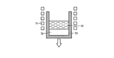
- FIG. 5 is a schematic configuration diagram of an example of a cast silicon growth apparatus of Comparative Example 1; It is a figure which shows the relationship between the nitrogen concentration (atoms / cm ⁇ 3 >) of the silicon ribbon of the photovoltaic cell of Example 1, and the reverse direction leakage current (A) at the time of dark. It is a figure which shows the relationship between the nitrogen concentration (atoms / cm ⁇ 3 >) of the silicon ribbon of the photovoltaic cell of Example 2, and the reverse direction leakage current (A) at the time of dark. It is a figure which shows the relationship between the nitrogen concentration (atoms / cm ⁇ 3 >) of the silicon ribbon of the photovoltaic cell of Example 3, and the reverse direction leakage current (A) at the time of dark. It is a figure which shows the relationship between the nitrogen concentration (atoms / cm ⁇ 3 >) of the silicon ribbon of the photovoltaic cell of the comparative example 1, and the reverse direction leakage current (A) at the time of dark.
- the silicon ribbon of the present invention is a silicon ribbon produced directly from a melt, and is characterized in that the nitrogen concentration of the silicon ribbon is 5 ⁇ 10 15 atoms / cm 3 or more and 5 ⁇ 10 17 atoms / cm 3 or less. There is. This is because the inventors of the present invention conducted intensive studies and found that the reverse leakage of a solar cell produced using a silicon ribbon having a nitrogen concentration of 5 ⁇ 10 15 atoms / cm 3 or more and 5 ⁇ 10 17 atoms / cm 3 or less It is due to the finding that the current can be reduced.
- the pn junction in which nitrogen is formed in the silicon ribbon when the nitrogen concentration is 5 ⁇ 10 15 atoms / cm 3 or more and 5 ⁇ 10 17 atoms / cm 3 or less It is believed that reverse leakage current can be suppressed to passivate nearby defect levels.
- the nitrogen concentration of the silicon ribbon exceeds 5 ⁇ 10 17 atoms / cm 3 , it is considered that the reverse leakage current increases because defect levels due to high concentration of nitrogen appear in the silicon ribbon.
- the nitrogen concentration of the silicon ribbon of the present invention is preferably 1 ⁇ 10 16 atoms / cm 3 or more and 5 ⁇ 10 16 atoms / cm 3 or less.
- a solar battery cell is manufactured using a silicon ribbon having a nitrogen concentration of 1 ⁇ 10 16 atoms / cm 3 or more and 5 ⁇ 10 16 atoms / cm 3 or less, the reverse leakage current of the solar battery cell is further reduced Tends to be able to
- the nitrogen concentration of the silicon ribbon of the present invention corresponds to the total number of nitrogen atoms in the silicon ribbon divided by the volume of the silicon ribbon, and, for example, SIMS (secondary ion mass spectrometry) or CPAA (charged particle activation) It can calculate using analysis etc.
- SIMS secondary ion mass spectrometry
- CPAA charged particle activation
- the silicon ribbon of the present invention is characterized by being produced directly from the melt. The reason is that the growth rate is faster, the nitrogen segregation effect is less effective, and the behavior of nitrogen in the crystal is different, as compared to the casting method in which the crystalline silicon ingot needs to be prepared once by solidifying the melt. It is believed that there is. It is thought that nitrogen, which behaves in the same manner as the silicon ribbon of the present invention, is also contained in a silicon crystal substrate produced by a cast method, but such nitrogen is at the position described in Non-patent Document 1 It is considered that the influence of nitrogen on the reduction of the reverse leakage current is different, because it often occurs.
- the method for producing a silicon ribbon of the present invention includes (i) producing a nitrogen-containing silicon melt, and (ii) growing the silicon ribbon.
- the nitrogen-containing silicon melt contains, for example, nitrogen in a silicon melt produced using a conventionally known method.
- a method of containing nitrogen in the silicon melt for example, a method of introducing a gas containing nitrogen into a chamber in which the silicon melt is contained, a method of introducing silicon nitride into the silicon melt, or the like can be used.
- the nitrogen concentration in the nitrogen-containing silicon melt is adjusted, for example, by adjusting the nitrogen gas flow rate and nitrogen gas introduction time introduced into the chamber containing the silicon melt, or the amount of silicon nitride introduced into the silicon melt. It is possible to adjust suitably.
- the nitrogen concentration of the silicon ribbon grown in the following step (ii) is 5 ⁇ 10 15 atoms / cm 3 or more and 5 ⁇ 10 17 atoms / cm 3 or less, preferably 1 ⁇ 10 16 atoms / cm 3.
- the nitrogen concentration in the silicon melt is adjusted to be cm 3 or more 5 ⁇ 10 16 atoms / cm 3 or less.
- the nitrogen-containing silicon melt is, for example, a group III element such as B (boron), Al (aluminum), Ga (gallium), P (phosphorus), or the like, in order to make the silicon ribbon p-type or n-type. It may contain a group V element such as As (arsenic) or Sb (antimony).
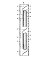
- FIG. 1 shows a schematic block diagram of an example of a silicon ribbon growth apparatus.
- the silicon ribbon growth apparatus shown in FIG. 1 includes a pedestal 26, a crucible 22 attached to the pedestal 26, and a pedestal 28 mounted on the opposite side to the ridge 22 of the pedestal 26 and a pedestal 26. , A heater 21 for heating the crucible 22, and a shaft 29 provided above the crucible 22.
- the growth apparatus of the silicon ribbon shown by FIG. 1 is installed in the chamber so that evacuation can be performed.
- the growth apparatus of silicon ribbon shown in FIG. 1 is, for example, an apparatus for moving the axis 29 in the direction of the arrow in FIG. 1, an apparatus for controlling the heater 21 and nitrogen It may have a device for additionally charging the silicon melt to the crucible 22 or the like.
- the step of growing a silicon ribbon using the silicon ribbon growth apparatus shown in FIG. 1 is performed, for example, as follows. First, the nitrogen-containing silicon melt 12 prepared in the above step (i) is contained in the crucible 22 and the temperature of the nitrogen-containing silicon melt 12 in the crucible 22 is set to, for example, 1420 ° C. Hold at about 1440 ° C.
- the silicon ribbon growth substrate 14 is attached to the tip of the shaft 29, and the shaft 29 is moved in the direction of the arrow in FIG.
- the surface of the silicon ribbon growth substrate 14 is immersed in the nitrogen-containing silicon melt 12 inside the crucible 22, and the silicon ribbon growth substrate 14 is brought into contact with the nitrogen-containing silicon melt 12.
- the silicon ribbon growth substrate 14 is preferably made of a material having good thermal conductivity and / or a material having excellent heat resistance. Examples of such a material include graphite, silicon carbide and boron nitride. .
- the immersion time of the surface of the silicon ribbon growth substrate 14 in the nitrogen-containing silicon melt 12 can take an appropriate time depending on the desired thickness of the silicon ribbon 11, but for example, to obtain the silicon ribbon 11 with a thickness of 300 ⁇ m.
- the immersion time is about 3 to 4 seconds.
- the nitrogen concentration on the surface of the silicon ribbon growth substrate 14 is 5 ⁇ 10 15 atoms / cm 3 or more and 5 ⁇ 10 17 atoms / cm 3 or less, preferably 1 ⁇ 10 16 atoms / cm 3 or more and 5 ⁇ 10 16 A silicon ribbon 11 having atoms / cm 3 or less is grown.
- the growth rate of the silicon ribbon 11 is preferably 20 ⁇ m / second or more.
- nitrogen that can effectively reduce the reverse leakage current can be efficiently incorporated into the silicon ribbon 11, and such nitrogen can be reduced.
- the incorporated silicon ribbon 11 can be manufactured stably and efficiently. Therefore, there is a tendency that the silicon ribbon 11 capable of effectively reducing the reverse leakage current in the solar battery cell can be manufactured with a good manufacturing yield and at low cost.
- the growth rate of the silicon ribbon 11 is the growth rate of the silicon ribbon 11 in the direction perpendicular to the surface of the silicon ribbon growth substrate 14.
- the surface of the silicon ribbon growth substrate 14 is pulled away from the nitrogen-containing silicon melt 12 by further moving the shaft 29 in the direction of the arrow in FIG. 1, and the silicon ribbon 11 is removed from the silicon ribbon growth substrate 14
- the silicon ribbon 11 of the present invention can be produced.
- two plate-like members 13 are immersed in the nitrogen-containing silicon melt 12 produced in the above step (i) at a distance from each other.
- a graphite plate can be used as the plate-like body 13.
- the nitrogen-containing silicon melt 12 is drawn in the direction of the arrow 15 from between the two plates 13 to cool the nitrogen-containing silicon melt 12 so that the nitrogen concentration is 5 ⁇ 10 15 atoms / cm 3.
- the silicon ribbon 11 of the present invention is grown to be 5 ⁇ 10 17 atoms / cm 3 or less, preferably 1 ⁇ 10 16 atoms / cm 3 or more and 5 ⁇ 10 16 atoms / cm 3 or less.
- the reduction effect of reverse leakage current by nitrogen in the silicon ribbon 11 of the present invention is in principle positively correlated with the growth rate of the silicon ribbon.
- the silicon ribbon manufacturing method is roughly divided into two types, a group using no silicon ribbon growth substrate and a group in which a silicon ribbon is grown on a silicon ribbon growth substrate using a silicon ribbon growth substrate. . In the latter group, since the heat removal from the silicon ribbon growth substrate is possible, the growth rate of the silicon ribbon can be increased compared to the former group, and the reverse leakage current of the silicon ribbon by nitrogen can be achieved.
- EFG Edge-Defined Film-fed Growth
- String Ribbon registered trademark
- RGS Rabbon Growth on Substrate
- RST Rabbon on Sacrificial Carbon Template
- a p-type silicon ribbon 11 is prepared, and texture etching of the silicon ribbon 11 is performed to form a texture structure (not shown) on the surface of the silicon ribbon 11.
- PSG (phosphosilicate glass) liquid 31 is applied to the surface of the silicon ribbon 11 on the light receiving surface side of the solar battery cell.
- the solar battery cell of the silicon ribbon 11 is diffused by diffusing phosphorus from the PSG liquid 31 to the silicon ribbon 11 by heating the silicon ribbon 11 after the application of the PSG liquid 31.
- the n + layer 32 is formed on the surface on the light receiving surface side of At this time, a PSG film 31 a is formed on the n + layer 32.
- the PSG film 31a formed during the diffusion of phosphorus is removed.
- an antireflective film 33 such as a silicon nitride film is formed on the n + layer 32 of the silicon ribbon 11.
- an aluminum paste 34 is applied to the front surface (back surface) of the silicon ribbon 11 that is the back surface side of the solar battery cell. Then, by baking the silicon ribbon 11 after the application of the aluminum paste 34, aluminum is diffused from the aluminum paste 34 to the back surface of the silicon ribbon 11, and as shown in FIG. An aluminum electrode 34a and ap + layer 35 are simultaneously formed.
- a silver paste 36a is applied on the surface of the anti-reflection film 33, and then baked, as shown in FIG. 3 (i). Forming a silver electrode 36 connected in the same manner. Thereafter, a solder is applied to the silver electrode 36 to produce an example of a solar cell using the silicon ribbon of the present invention.
- FIG. 4 shows a schematic cross-sectional view of an example of a solar cell module including the solar cell manufactured as described above.
- the solar cell module is formed by electrically connecting a plurality of solar cells manufactured using the silicon ribbon of the present invention in series.
- the silver electrodes 36 on the light receiving surface side of one solar battery cell and the aluminum electrodes 34 a on the back surface side of the other solar battery cells, which are arranged adjacent to each other, are said to be conductive, which is said to be an interconnector
- these solar cells are electrically connected in series to constitute a solar cell string.
- a solar cell module is produced by sealing the above-mentioned solar cell string in the sealing material 42 installed between the transparent substrate 41 and the protective sheet 43.
- the transparent substrate 41 for example, a glass substrate can be used.
- the protective sheet 43 for example, a PET (polyethylene terephthalate) film or the like can be used.
- the sealing material 42 for example, a transparent resin such as EVA (ethylene vinyl acetate) can be used.
- the solar cell and the solar cell module manufactured as described above have a nitrogen concentration of 5 ⁇ 10 15 atoms / cm 3 or more and 5 ⁇ 10 17 atoms / cm 3 or less, preferably 1 ⁇ 10 16 atoms / cm 3 or more Since the silicon ribbon 11 of the present invention, which is 5 ⁇ 10 16 atoms / cm 3 or less, is used, the reverse leakage current in the solar battery cell is reduced. Therefore, the incidence rate of defective products due to the large reverse leakage current is reduced, so that solar cells and solar cell modules having good characteristics can be manufactured with high manufacturing yield and low cost.
- the conventionally well-known structure can be used for the photovoltaic cell of this invention, and a solar cell module except using the silicon ribbon of this invention.
- a structure in which an n + layer is formed on a p-type silicon ribbon of the present invention, a structure in which a p + layer is formed on an n-type silicon ribbon of the present invention, a structure in which a heterojunction with thin film silicon etc. is formed, and MIS (Metal Insulator Semiconductor) structure etc. may be sufficient.
- a conventionally well-known method can be used.
- the spherical silicon of the present invention is spherical silicon produced directly from the melt, and the nitrogen concentration of the spherical silicon is 5 ⁇ 10 15 atoms / cm 3 or more and 5 ⁇ 10 17 atoms / cm 3 or less. There is. As a result of intensive studies conducted by the present inventor, the reverse is also true for a solar battery cell manufactured using spherical silicon having a nitrogen concentration of 5 ⁇ 10 15 atoms / cm 3 or more and 5 ⁇ 10 17 atoms / cm 3 or less. This is due to the finding that the directional leakage current can be reduced.
- the pn junction in which nitrogen is formed in spherical silicon when the nitrogen concentration is 5 ⁇ 10 15 atoms / cm 3 or more and 5 ⁇ 10 17 atoms / cm 3 or less It is believed that reverse leakage current can be suppressed to passivate nearby defect levels.
- the nitrogen concentration of the spherical silicon exceeds 5 ⁇ 10 17 atoms / cm 3 , it is considered that the reverse leakage current increases because defect levels due to high concentration of nitrogen appear in the spherical silicon.
- the nitrogen concentration of the spherical silicon of the present invention is preferably 1 ⁇ 10 16 atoms / cm 3 or more and 5 ⁇ 10 16 atoms / cm 3 or less.
- the reverse leakage current of the solar cell is further reduced Tends to be able to
- the nitrogen concentration of the spherical silicon of the present invention corresponds to the total number of nitrogen atoms in the spherical silicon divided by the volume of the spherical silicon, and can be calculated using, for example, SIMS or CPAA.
- the spherical silicon of the present invention is characterized by being produced directly from the melt. The reason is that the growth rate is faster, the nitrogen segregation effect is less effective, and the behavior of nitrogen in the crystal is different, compared to the casting method where it is necessary to solidify the melt and make a large crystalline silicon ingot once. It is considered to be. It is thought that nitrogen, which behaves in the same manner as the silicon ribbon of the present invention, is contained in the silicon crystal substrate produced by the casting method, but such nitrogen is at the position (in SiC) described in Non-Patent Document 1. As it is often present, the influence of nitrogen on reducing the reverse leakage current is considered to be different.
- the method for producing spherical silicon of the present invention includes the steps of (I) producing a nitrogen-containing silicon melt and (II) growing spherical silicon.
- the process of producing (I) nitrogen-containing silicon melt is the same as the process of said (i), it abbreviate
- FIG. 5 shows a schematic block diagram of an example of a spherical silicon growth apparatus.
- the apparatus for growing spherical silicon shown in FIG. 5 includes a chamber 51, a crucible 55 disposed above the interior of the chamber 51, a heater 52 disposed around the crucible 55, and a lower part of the chamber 51. And a collection container 54 installed.
- the step of growing spherical silicon using the spherical silicon growth apparatus shown in FIG. 5 is performed, for example, as follows.
- the atmosphere inside the chamber 51 is, for example, an argon gas atmosphere, and the nitrogen-containing silicon melt 12 produced in the above step (I) is accommodated in the crucible 55. Then, the temperature of the nitrogen-containing silicon melt 12 inside the crucible 55 is maintained at, for example, about 1420 ° C. to 1440 ° C. by the heater 52.
- the nitrogen-containing silicon melt 12 is dropped into the chamber 51 from the opening provided in the lower part of the crucible 55. At this time, the nitrogen-containing silicon melt 12 is dropped from the crucible 55 in the form of droplets, and the drop-like nitrogen-containing silicon melt 12 is cooled and solidified inside the chamber 51 while falling, thereby forming spherical silicon 53. Will grow.
- the spherical silicon 53 grown during the fall is contained in a collection container 54 provided at the lower part inside the chamber 51, so that the nitrogen concentration is 5 ⁇ 10 15 atoms / cm 3 or more and 5 ⁇ 10 17.
- the growth rate of the spherical silicon 53 is preferably 20 ⁇ m / second or more, and more preferably 25 ⁇ m / second or more.
- the growth rate of the spherical silicon 53 is 20 ⁇ m / sec or more, particularly 25 ⁇ m / sec or more, nitrogen capable of effectively reducing the reverse leakage current can be efficiently incorporated into the spherical silicon 53.
- spherical silicon 53 containing such nitrogen can be stably and efficiently produced. Therefore, there is a tendency that spherical silicon 53 capable of effectively reducing reverse leakage current in a solar battery cell can be manufactured at a good manufacturing yield and at low cost.
- the growth rate of the spherical silicon 53 mentioned here means a value obtained by dividing the minimum value of the distance between the position of the crystal nucleus and the crystal plane (growth front) of the crystal grown from the crystal nucleus by the growth time. doing.
- FIG. 6 shows a schematic cross-sectional view of an example of a solar cell using spherical silicon of the present invention.
- the solar battery cell shown in FIG. 6 includes p-type spherical silicon 53, n + layer 61 formed on the outer surface of spherical silicon 53, conductive sheet 66 in contact with p-type spherical silicon 53, and n + layer 61 formed on the surface of n + layer 61, conductive sheet 64 in contact with 61, insulating layer 65 disposed between conductive sheet 66 and conductive sheet 64 to electrically insulate them
- An antireflective film 62 and a transparent protective film 63 covering the antireflective film 62 and the conductive sheet 64 are provided.
- an aluminum foil or the like can be used as the conductive sheets 64 and 66, respectively.
- the insulating layer 65 for example, polyimide or the like can be used.
- silicon nitride or titanium oxide can be used as the antireflective film 62.
- the transparent protective film 63 for example, a transparent plastic film or the like can be used.
- the solar battery cell shown in FIG. 6 can be manufactured, for example, as follows. First, a plurality of p-type spherical silicons 53 are prepared, and an n + -type layer 61 is formed by diffusing an n-type dopant such as phosphorus on the outer surface of these p-type spherical silicons 53.
- each of the spherical silicon 53 after the formation of the n + layer 61 is placed in the hole of the holed conductive sheet 64, and the n + layer 61 exposed on the back surface side from the hole of the conductive sheet 64 is removed by etching Do.
- a part of the insulating layer 65 is removed to expose the surface of the p-type spherical silicon 53, and the conductive on the surface of the exposed spherical silicon 53 Install the sex sheet 66.
- the antireflective film 62 is formed on the surface of the n + layer 61 on the surface side of the conductive sheet 64, and then the antireflective film 62 and the conductive sheet 64 are covered with the transparent protective film 63.
- a plurality of solar cells manufactured as described above are electrically connected in series to form a solar cell string, and the above solar cell string is disposed between the transparent substrate and the protective sheet.
- the solar cell module is manufactured by being sealed in the sealing material.
- the solar cell and the solar cell module manufactured as described above have a nitrogen concentration of 5 ⁇ 10 15 atoms / cm 3 or more and 5 ⁇ 10 17 atoms / cm 3 or less, preferably 1 ⁇ 10 16 atoms / cm 3 or more Since the spherical silicon 53 of the present invention, which is 5 ⁇ 10 16 atoms / cm 3 or less, is used, the reverse leakage current in the solar battery cell is reduced. Therefore, the incidence rate of defective products due to the large reverse leakage current is reduced, so that solar cells and solar cell modules having good characteristics can be manufactured with high manufacturing yield and low cost.
- the conventionally well-known structure can be used for the photovoltaic cell of this invention, and a solar cell module except using the spherical silicon of this invention.
- a structure in which an n + layer is formed on p-type spherical silicon according to the present invention, a structure in which ap + layer is formed on n-type spherical silicon according to the present invention, a structure in which a heterojunction with thin silicon is formed, and MIS (Metal Insulator Semiconductor) structure etc. may be sufficient.
- a conventionally well-known method can be used.
- a silicon ribbon was produced by performing the steps of (i) producing a nitrogen-containing silicon melt and (ii) growing the silicon ribbon using the silicon ribbon growth apparatus shown in FIG.
- the silicon raw material is melted by heating the crucible 22 by the heater 21 and then the temperature is raised to 1550 ° C. to confirm that the silicon raw material is completely dissolved, and then argon gas is introduced into the chamber. Together with a small amount of nitrogen gas for 5 hours.
- the flow ratio of nitrogen gas to argon gas was about 1: 2
- the flow rate of the mixed gas of nitrogen gas and argon gas was 90 L / min.
- the surface of the silicon ribbon growth substrate 14 made of graphite attached to the tip of the shaft 29 is immersed in the nitrogen-containing silicon melt 12 obtained as described above under the condition that the immersion time is 2 seconds.
- the silicon ribbon 11 was grown on the surface of the silicon ribbon growth substrate 14.
- the thickness of the silicon ribbon 11 thus obtained was 280 ⁇ m on average in the plane (the growth rate of 140 ⁇ m / second).
- the preparation of the silicon ribbon 11 is continued until the nitrogen-containing silicon melt 12 reaches 50 kg, and then the boron concentration is adjusted so that the specific resistance is 3 ⁇ ⁇ cm. 50 kg of the silicon raw material thus prepared was charged into the crucible 22. Then, without introducing nitrogen gas into the chamber, the silicon source was melted to produce a nitrogen-containing silicon melt 12 in which the nitrogen concentration was reduced. Then, the silicon ribbon 11 was grown by the same method and the same condition as described above. This process was repeated to gradually reduce the nitrogen concentration of the nitrogen-containing silicon melt 12 to produce nitrogen-containing silicon melts 12 of various nitrogen concentrations, thereby growing silicon ribbons 11 of various nitrogen concentrations.
- Spherical silicon was produced by performing the steps of (I) producing a nitrogen-containing silicon melt and (II) growing the spherical silicon using the apparatus for growing spherical silicon shown in FIG.
- the silicon material is melted by heating the crucible 55 by the heater 52, and then the temperature is raised to 1550 ° C. to confirm that the silicon material is completely dissolved.
- a small amount of nitrogen gas was introduced together with the gas for 5 hours.
- the flow ratio of nitrogen gas to argon gas was about 1: 2
- the flow rate of the mixed gas of nitrogen gas and argon gas was 90 L / min.
- the nitrogen-containing silicon melt 12 obtained as described above was dropped about 10 m from the opening provided in the lower part of the crucible 55 to the lower part of the chamber 51.
- the nitrogen-containing silicon melt 12 is dropped from the crucible 55 in the form of droplets, and the drop-like nitrogen-containing silicon melt 12 is cooled and solidified inside the chamber 51 while falling, thereby forming spherical silicon 53.
- the spherical silicon 53 grown during falling was accommodated in a collecting container 54 provided at the lower part inside the chamber 51 and collected.
- the growth rate of spherical silicon 53 was 25 ⁇ m / sec.
- the preparation of the spherical silicon 53 is continued until the nitrogen-containing silicon melt 12 reaches 50 kg, and then the boron concentration is adjusted so that the specific resistance is 3 ⁇ ⁇ cm. 50 kg of the silicon raw material thus prepared was charged into a crucible 55. Then, without introducing nitrogen gas into the chamber, the silicon source was melted to produce a nitrogen-containing silicon melt 12 in which the nitrogen concentration was reduced. Then, spherical silicon 53 was grown by the same method and the same conditions as described above. By repeating this process, the nitrogen concentration of the nitrogen-containing silicon melt 12 is gradually reduced to prepare the nitrogen-containing silicon melt 12 of various nitrogen concentrations, and spherical silicon 53 of various nitrogen concentrations is grown.
- a silicon ribbon was manufactured by performing the steps of (i) preparing a nitrogen-containing silicon melt and (ii) growing a silicon ribbon using the silicon ribbon growth apparatus shown in FIG.
- the silicon raw material is melted by heating the crucible with a heater (not shown), and after raising the temperature to 1550 ° C., it is confirmed that the silicon raw material is completely dissolved, and then the inside of the chamber is formed.
- a small amount of nitrogen gas was introduced for 5 hours together with argon gas.
- the flow ratio of nitrogen gas to argon gas was about 1: 2
- the flow rate of the mixed gas of nitrogen gas and argon gas was 90 L / min.
- a plate-like body 13 consisting of two graphite plates was immersed in the nitrogen-containing silicon melt 12 at a distance from each other.
- the silicon ribbon 11 was produced by pulling up the nitrogen-containing silicon melt 12 in the direction of the arrow 15 from between the two plate-like members 13 at a pulling rate of about 85 ⁇ s / sec. At this time, the growth rate of the silicon ribbon 11 was 85 ⁇ m / second.
- the preparation of the silicon ribbon 11 is continued until the nitrogen-containing silicon melt 12 reaches 50 kg, and then the boron concentration is adjusted so that the specific resistance is 3 ⁇ ⁇ cm. 50 kg of the raw material of silicon was put into the crucible. Then, without introducing nitrogen gas into the chamber, the silicon source was melted to produce a nitrogen-containing silicon melt 12 in which the nitrogen concentration was reduced. Then, the silicon ribbon 11 was grown by the same method and the same condition as described above. This process was repeated to gradually reduce the nitrogen concentration of the nitrogen-containing silicon melt 12 to produce nitrogen-containing silicon melts 12 of various nitrogen concentrations, thereby growing silicon ribbons 11 of various nitrogen concentrations.
- cast silicon was produced by performing (A) a step of producing a nitrogen-containing silicon melt and (B) a step of growing cast silicon.
- a silica mold 73 (having a square opening with an inner diameter of 830 mm) coated with a mold release material made of silicon nitride on the inner circumferential surface is filled with 400 kg of silicon raw material, and the silica heater 73 is heated by the heater 71 Then, the silicon source was melted and then heated to 1550 ° C. to confirm that the silicon source was completely dissolved, and then a small amount of nitrogen gas was introduced into the chamber together with argon gas for 5 hours.
- the flow ratio of nitrogen gas to argon gas was about 1: 2
- the flow rate of the mixed gas of nitrogen gas and argon gas was 90 L / min.
- cast silicon 72 was grown by lowering the set temperature of the heater 71 at a rate of 0.5 ° C./hour and lowering the height of the silica crucible 73 at a speed of 8 mm / hour.
- the growth rate of cast silicon 72 was 3 ⁇ m / sec.
- the preparation of cast silicon 72 is continued until the nitrogen-containing silicon melt 12 reaches 50 kg, and then the boron concentration is adjusted so that the specific resistance is 3 ⁇ ⁇ cm. 50 kg of the silicon raw material was charged into the crucible. Then, without introducing nitrogen gas into the chamber, the silicon source was melted to produce a nitrogen-containing silicon melt 12 in which the nitrogen concentration was reduced. Then, cast silicon 72 was grown by the same method and conditions as described above. This process was repeated to gradually reduce the nitrogen concentration of the nitrogen-containing silicon melt 12 to produce nitrogen-containing silicon melts 12 of various nitrogen concentrations, and cast silicon 72 of various nitrogen concentrations was grown.
- Secondary ion mass spectrometer made by CAMECA, IMS-6F
- Primary ion Cs +
- Acceleration voltage 10 kV
- Secondary Detection ion 29 Si 14 N -
- Secondary extraction voltage 4.5kV
- Primary current 100 nA
- Primary beam scan area 80 ⁇ m ⁇
- Data acquisition area 33 ⁇ m ⁇
- Measurement time 1 second / point.
- Example 1 a 280 ⁇ m thick p-type silicon ribbon manufactured in Example 1 was cut using a laser to manufacture the p-type silicon ribbon 11 shown in FIG. 3A having a square surface of 155 mm ⁇ 155 mm. .
- the silicon ribbon 11 was immersed in an aqueous solution of sodium hydroxide to perform anisotropic etching of the silicon ribbon 11, thereby forming a texture structure (not shown) on the surface of the silicon ribbon 11.
- PSG liquid 31 was applied by spin coating on the surface of the silicon ribbon 11 which is to be the light receiving surface side of the solar battery cell.
- phosphorus is diffused from the PSG liquid 31 to the silicon ribbon 11 by placing the silicon ribbon 11 after application of the PSG liquid 31 in a diffusion furnace and heating the silicon ribbon 11, as shown in FIG.
- the n + layer 32 was formed on the surface on the light receiving surface side of the solar cell.
- the PSG film 31a formed during the diffusion of phosphorus was removed.
- an antireflective film 33 made of a silicon nitride film was formed on the n + layer 32 of the silicon ribbon 11 by plasma CVD.
- an aluminum paste 34 was applied by screen printing on the surface (back surface) of the silicon ribbon 11 to be the back surface side of the solar battery cell. Then, by baking the silicon ribbon 11 after the application of the aluminum paste 34, aluminum is diffused from the aluminum paste 34 to the back surface of the silicon ribbon 11, and aluminum is formed on the back surface of the silicon ribbon 11 as shown in FIG.
- the electrode 34a and the p + layer 35 were simultaneously formed.
- a silver paste 36a is applied in a predetermined shape by screen printing on the surface of the anti-reflection film 33 and then fired, as shown in FIG. 3 (i). , And the silver electrode 36 electrically connected to the n + layer 32 were formed. Then, the solar battery cell of Example 1 was produced by carrying out the solder dip to the silver electrode 36.
- FIG. 3 (h) When the n + layer 32 contacts the aluminum electrode 34 a on the back surface at the peripheral portion of the silicon ribbon 11, the fill factor (FF) of the solar cell decreases and the conversion efficiency decreases, so the n + layer 32 and the aluminum electrode 34 a Junction separation with
- the above-described solar battery cell manufacturing process was performed for each of the silicon ribbons of Example 1 having different nitrogen concentrations, and a plurality of solar battery cells of Example 1 having different nitrogen concentrations of silicon ribbons were manufactured.
- the reverse direction leak current at the time of dark was measured about each of a photovoltaic cell of Example 1 produced as mentioned above.
- the results are shown in FIG.
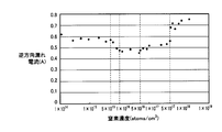
- the horizontal axis of FIG. 8 indicates the nitrogen concentration (atoms / cm 3 ) of the silicon ribbon of the solar battery cell of Example 1, and the vertical axis indicates the reverse leakage current (A) in the dark.
- the reverse direction leakage current at dark time applies a positive voltage of +10 V to the silver electrode 36 side of the solar battery cell in a state where the solar battery cell of Example 1 is not irradiated with light, and measures the current flowing in the solar battery cell It asked by.
- the reverse leakage current in the dark becomes small. If the nitrogen concentration of the silicon ribbon is in the range of 1 ⁇ 10 16 atoms / cm 3 or more and 5 ⁇ 10 16 atoms / cm 3 or less, the reverse leakage current in the dark tends to be particularly small. It was confirmed that there is.
- the nitrogen concentration in the horizontal axis of FIG. 8 is the measurement result using the above-mentioned SIMS, and not only all solid solution in silicon ribbon but necessarily in the form of nitride such as Si 3 N 4 Things are also included.
- the growth speed of the silicon ribbon is changed from 20 ⁇ m / second to 300 ⁇ m / second by changing the temperature of the crucible 22 at the time of growth of the silicon ribbon and the conditions for immersing the surface of the substrate 14 for silicon ribbon growth in the nitrogen-containing silicon melt 12. Silicon ribbons were manufactured and evaluated in the same manner, but the same results as FIG. 8 were obtained.
- Example 2 A solar cell having a structure shown in FIG. 6 in which the nitrogen concentration of spherical silicon is different from each other by using spherical silicon of various nitrogen concentrations manufactured in Example 2 described above was manufactured as follows.
- a plurality of p-type spherical silicons 53 manufactured in Example 2 were prepared, and phosphorus was diffused on the outer surface of each of the p-type spherical silicons 53 to form an n + layer 61.
- each of the spherical silicon 53 after the formation of the n + layer 61 is placed in the hole of the conductive sheet 64 made of aluminum foil with holes, and the n + layer 61 exposed on the back side from the hole of the conductive sheet 64 was removed by etching.
- insulating layer 65 made of polyimide is formed on the back surface of the conductive sheet 64.
- a part of the insulating layer 65 is removed to expose the surface of the p-type spherical silicon 53, and the exposed spherical silicon 53 is formed.
- a conductive sheet 66 made of aluminum foil was placed on the surface.
- an antireflective film 62 made of titanium oxide is formed on the surface of the n + layer 61 on the surface side of the conductive sheet 64, and thereafter, the antireflective film 62 and the conductive sheet 64 are transparent made of a transparent plastic film.
- a solar battery cell of Example 2 was produced.
- the above-described solar battery cell manufacturing process was performed for each of the spherical silicon particles of Example 2 having different nitrogen concentrations, and a plurality of solar battery cells of Example 2 having different nitrogen concentrations of spherical silicon particles were manufactured.
- the reverse direction leak current at the time of dark was measured about each of a photovoltaic cell of Example 2 produced as mentioned above.
- the results are shown in FIG.
- the horizontal axis of FIG. 9 indicates the nitrogen concentration (atoms / cm 3 ) of the silicon ribbon of the solar battery cell of Example 2, and the vertical axis indicates the reverse leakage current (A) in the dark.
- the reverse direction leakage current at the time of dark applies a positive voltage of +10 V to the conductive sheet 64 side of the solar battery cell in a state where the solar battery cell of Example 2 is not irradiated with light, and measures the current flowing in the solar battery cell It asked by doing.
- Example 3 The solar battery cell of Example 3 in which the nitrogen concentrations of the silicon ribbons were different from each other was manufactured in the same manner as in Example 1 using the silicon ribbons of various nitrogen concentrations manufactured in Example 3 described above.
- Example 3 And about each of the photovoltaic cell of Example 3, it carried out similarly to Example 1, and measured the reverse direction leakage current at the time of dark. The results are shown in FIG.
- the horizontal axis of FIG. 10 indicates the nitrogen concentration (atoms / cm 3 ) of the silicon ribbon of the solar battery cell of Example 3, and the vertical axis indicates the reverse leakage current (A) in the dark.
- the reverse direction leakage current at dark time applies a positive voltage of +10 V to the silver electrode 36 side of the solar battery cell in a state where the solar battery cell of Example 3 is not irradiated with light, and measures the current flowing in the solar battery cell It asked by.
- the reverse leakage current in the dark becomes small. If the nitrogen concentration of the silicon ribbon is in the range of 1 ⁇ 10 16 atoms / cm 3 or more and 5 ⁇ 10 16 atoms / cm 3 or less, the reverse leakage current in the dark tends to be particularly small. It was confirmed that there is.
- each of the photovoltaic cell of the comparative example 1 it carried out similarly to Example 1, and measured the reverse direction leakage current at the time of dark.
- the results are shown in FIG.
- the horizontal axis of FIG. 11 indicates the nitrogen concentration (atoms / cm 3 ) of the silicon ribbon of the solar battery cell of Comparative Example 1, and the vertical axis indicates the reverse leakage current (A) in the dark.
- the reverse direction leakage current at dark time applies a positive voltage of +10 V to the silver electrode 36 side of the solar battery cell in a state where the solar battery cell of Comparative Example 1 is not irradiated with light, and measures the current flowing in the solar battery cell. It asked by.
- the present invention may be applicable to silicon ribbons, spherical silicon, solar cells, solar cell modules, methods of manufacturing silicon ribbons, and methods of manufacturing spherical silicon.
Landscapes
- Chemical & Material Sciences (AREA)
- Organic Chemistry (AREA)
- Crystallography & Structural Chemistry (AREA)
- Engineering & Computer Science (AREA)
- Materials Engineering (AREA)
- Metallurgy (AREA)
- Inorganic Chemistry (AREA)
- Photovoltaic Devices (AREA)
- Silicon Compounds (AREA)
- Crystals, And After-Treatments Of Crystals (AREA)
- Liquid Deposition Of Substances Of Which Semiconductor Devices Are Composed (AREA)
Abstract
Description
(1)シリコン融液を凝固させて大きなシリコン結晶インゴットを作製し、シリコン結晶インゴットをスライスする方法(キャスト法)。
(2)シリコン融液に成長用基板を接触させることなく、直接ウエハの形状にシリコンリボンを成長させる方法。
(3)シリコン融液に成長用基板を接触させて、成長用基板上にシリコンリボンを成長させる方法。
(4)シリコン融液を不活性ガス中などに滴下して落下中に凝固させ、またはシリコン融液を小さな鋳型に投入して凝固させることによって球状シリコンを成長させる方法。
(a)太陽電池セル側面における不十分な接合分離。
(b)太陽電池セルの受光面のn電極のp層への突き抜け。
(c)シリコン結晶基板の割れ部へのリンあるいはアルミニウムなどのドーパントの滲み出しあるいは貫通。
(d)pn接合部における欠陥準位あるいは不純物準位。
また、本発明は、上記の太陽電池セルを含む、太陽電池モジュールである。
また、本発明は、上記の太陽電池セルを含む、太陽電池モジュールである。
本発明のシリコンリボンは、融液から直接作製されるシリコンリボンであって、シリコンリボンの窒素濃度が5×10¹⁵atoms/cm3以上5×1017atoms/cm3以下であることを特徴としている。これは、本発明者が鋭意検討した結果、窒素濃度が5×1015atoms/cm3以上5×1017atoms/cm3以下であるシリコンリボンを用いて作製された太陽電池セルの逆方向漏れ電流を低減することができることを見出したことによるものである。逆方向漏れ電流を低減できるメカニズムは必ずしも明らかではないが、窒素濃度が5×1015atoms/cm3以上5×1017atoms/cm3以下のあたりで、窒素がシリコンリボンに形成されたpn接合近傍の欠陥準位をパッシベートするために逆方向漏れ電流を抑えることができると考えられる。シリコンリボンの窒素濃度が5×1017atoms/cm3を超える場合には、シリコンリボンに高濃度の窒素に起因する欠陥準位が現れるために、逆方向漏れ電流が増加すると考えられる。
本発明のシリコンリボンは、融液から直接作製されることを特徴としている。その理由は、融液を凝固させて結晶シリコンインゴットを一旦作製する必要のあるキャスト法と比較して、成長速度が速く、窒素の偏析効果が効きにくく、結晶中における窒素の振る舞いが異なるためであると考えられる。キャスト法で作製されたシリコン結晶基板中においても本発明のシリコンリボンと同様の振る舞いをする窒素は含まれると考えられるが、そのような窒素は非特許文献1に記載の位置(SiC中に存在)することが多いため、逆方向漏れ電流の低減に与える窒素の影響が異なっているものと考えられる。
窒素含有シリコン融液を作製する工程において、窒素含有シリコン融液は、たとえば、従来公知の方法を用いて作製されたシリコン融液に窒素を含有させることにより作製することができる。シリコン融液に窒素を含有させる方法としては、たとえば、シリコン融液が収容されたチャンバに窒素を含むガスを導入する方法、またはシリコン融液に窒化シリコンを投入する方法などを用いることができる。窒素含有シリコン融液中の窒素濃度は、たとえば、シリコン融液が収容されたチャンバに導入される窒素ガス流量および窒素ガス導入時間、またはシリコン融液への窒化シリコンの投入量を調整することにより適宜調整することが可能である。したがって、この工程においては、下記の(ii)の工程で成長するシリコンリボンの窒素濃度が5×10¹⁵atoms/cm3以上5×1017atoms/cm3以下、好ましくは1×1016atoms/cm3以上5×1016atoms/cm3以下となるようにシリコン融液中の窒素濃度が調整される。なお、窒素含有シリコン融液は、シリコンリボンをp型またはn型とするために、たとえば、B(ホウ素)、Al(アルミニウム)、Ga(ガリウム)などのIII族元素や、P(リン)、As(ヒ素)、Sb(アンチモン)などのV族元素などを含んでいてもよい。
上記の(i)の工程で作製された窒素含有シリコン融液からシリコンリボンを成長させて、本発明のシリコンリボンを窒素含有シリコン融液から直接作製する。図1に、シリコンリボンの成長装置の一例の模式的な構成図を示す。
以下、図3(a)~図3(i)の模式的断面図を参照して、本発明のシリコンリボンを用いて太陽電池セルを作製する方法の一例について説明する。
本発明の球状シリコンは、融液から直接作製される球状シリコンであって、球状シリコンの窒素濃度が5×10¹⁵atoms/cm3以上5×1017atoms/cm3以下であることを特徴としている。これは、本発明者が鋭意検討した結果、窒素濃度が5×1015atoms/cm3以上5×1017atoms/cm3以下である球状シリコンを用いて作製された太陽電池セルについてもその逆方向漏れ電流を低減することができることを見出したことによるものである。逆方向漏れ電流を低減できるメカニズムは必ずしも明らかではないが、窒素濃度が5×1015atoms/cm3以上5×1017atoms/cm3以下のあたりで、窒素が球状シリコンに形成されたpn接合近傍の欠陥準位をパッシベートするために逆方向漏れ電流を抑えることができると考えられる。球状シリコンの窒素濃度が5×1017atoms/cm3を超える場合には、球状シリコンに高濃度の窒素に起因する欠陥準位が現れるために、逆方向漏れ電流が増加すると考えられる。
本発明の球状シリコンは、融液から直接作製されることを特徴としている。その理由は、融液を凝固させて大きな結晶シリコンインゴットを一旦作製する必要のあるキャスト法と比較して、成長速度が速く、窒素の偏析効果が効きにくく、結晶中における窒素の振る舞いが異なるためであると考えられる。キャスト法で作製されたシリコン結晶基板中においても本発明のシリコンリボンと同様の振る舞いをする窒素は含まれると考えられるが、そのような窒素は非特許文献1に記載の位置(SiC中)に存在することが多いため、逆方向漏れ電流の低減に与える窒素の影響が異なっているものと考えられる。
上記の(I)の工程で作製された窒素含有シリコン融液から球状シリコンを成長させて本発明の球状シリコンを窒素含有シリコン融液から直接作製する。図5に、球状シリコンの成長装置の一例の模式的な構成図を示す。
図6に、本発明の球状シリコンを用いた太陽電池セルの一例の模式的な断面図を示す。図6に示す太陽電池セルは、p型の球状シリコン53と、球状シリコン53の外表面に形成されたn+層61と、p型の球状シリコン53に接する導電性シート66と、n+層61に接する導電性シート64と、導電性シート66と導電性シート64との間に設置されてこれらを電気的に絶縁するための絶縁層65と、n+層61の表面上に形成された反射防止膜62と、反射防止膜62および導電性シート64を覆う透明保護膜63と、を有している。
図1に示すシリコンリボンの成長装置を用いて、(i)窒素含有シリコン融液を作製する工程および(ii)シリコンリボンを成長させる工程を行なうことによって、シリコンリボンを作製した。
図5に示す球状シリコンの成長装置を用いて、(I)窒素含有シリコン融液を作製する工程および(II)球状シリコンを成長させる工程を行なうことによって、球状シリコンを作製した。
図2に示すシリコンリボンの成長装置を用いて、(i)窒素含有シリコン融液を作製する工程および(ii)シリコンリボンを成長させる工程を行なうことによって、シリコンリボンを作製した。
図7に示すキャストシリコンの成長装置を用いて、(A)窒素含有シリコン融液を作製する工程および(B)キャストシリコンを成長させる工程を行なうことによって、キャストシリコンを作製した。
実施例1で作製したシリコンリボン、実施例2で作製した球状シリコン、実施例3で作製したシリコンリボン、および比較例1で作製したキャストシリコンのそれぞれについてSIMS(二次イオン質量分析法)を用いて窒素濃度の測定を行なった。窒素濃度の測定に用いた装置および条件は以下のとおりである。
装置:二次イオン質量分析計(CAMECA社製、IMS-6F)
一次イオン:Cs+、加速電圧:10kV、
二次検出イオン:29Si14N-、
二次引出電圧:4.5kV、
一次電流:100nA、
一次ビームスキャン領域:80μm□、
データ取込領域:33μmφ、
測定時間:1秒/ポイント。
上記の実施例1で作製した様々な窒素濃度のシリコンリボンをそれぞれ用いて互いにシリコンリボンの窒素濃度が異なる太陽電池セルを以下のようにして作製した。
上記の実施例2で作製した様々な窒素濃度の球状シリコンをそれぞれ用いて互いに球状シリコンの窒素濃度が異なる図6に示す構造を有する太陽電池セルを以下のようにして作製した。
上記の実施例3で作製した様々な窒素濃度のシリコンリボンをそれぞれ用いて互いにシリコンリボンの窒素濃度が異なる実施例3の太陽電池セルを実施例1と同様にして作製した。
上記の比較例1で作製した様々な窒素濃度のキャストシリコンをそれぞれ実施例1のシリコンリボンと同じ大きさに切断してシリコン結晶基板を作製し、これらのシリコン結晶基板を用いて互いにシリコン結晶基板の窒素濃度が異なる比較例1の太陽電池セルを実施例1と同様にして作製した。
Claims (15)
- 融液(12)から直接作製されるシリコンリボン(11)であって、前記シリコンリボン(11)の窒素濃度が5×10¹⁵atoms/cm3以上5×1017atoms/cm3以下である、シリコンリボン(11)。
- 前記窒素濃度が1×10¹⁶atoms/cm3以上5×1016atoms/cm3以下であることを特徴とする、請求項1に記載のシリコンリボン(11)。
- 請求項1または2に記載のシリコンリボン(11)を用いて作製された、太陽電池セル。
- 請求項3に記載の太陽電池セルを含む、太陽電池モジュール。
- 融液(12)から直接作製される球状シリコン(53)であって、前記球状シリコン(53)の窒素濃度が5×10¹⁵atoms/cm3以上5×1017atoms/cm3以下である、球状シリコン(53)。
- 前記窒素濃度が1×10¹⁶atoms/cm3以上5×1016atoms/cm3以下であることを特徴とする、請求項5に記載の球状シリコン(53)。
- 請求項5または6に記載の球状シリコン(53)を用いて作製された、太陽電池セル。
- 請求項7に記載の太陽電池セルを含む、太陽電池モジュール。
- 窒素含有シリコン融液(12)を作製する工程と、
前記窒素含有シリコン融液(12)から窒素濃度が5×10¹⁵atoms/cm3以上5×1017atoms/cm3以下であるシリコンリボン(11)を成長させる工程と、を含む、シリコンリボン(11)の製造方法。 - 前記シリコンリボン(11)を成長させる工程においては、前記窒素濃度が1×10¹⁶atoms/cm3以上5×1016atoms/cm3以下であるシリコンリボン(11)を成長させることを特徴とする、請求項9に記載のシリコンリボン(11)の製造方法。
- 前記シリコンリボン(11)を成長させる工程においては、前記シリコンリボン(11)を成長用基板(14)上に成長させることを特徴とする、請求項9または10に記載のシリコンリボン(11)の製造方法。
- 前記シリコンリボン(11)を成長させる工程においては、前記シリコンリボン(11)の成長速度が20μm/秒以上であることを特徴とする、請求項11に記載のシリコンリボン(11)の製造方法。
- 窒素含有シリコン融液(12)を作製する工程と、
前記窒素含有シリコン融液(12)を落下させることによって窒素濃度が5×10¹⁵atoms/cm3以上5×1017atoms/cm3以下である球状シリコン(53)を成長させる工程と、を含む、球状シリコン(53)の製造方法。 - 前記球状シリコン(53)を成長させる工程においては、前記窒素濃度が1×10¹⁶atoms/cm3以上5×1016atoms/cm3以下である球状シリコン(53)を成長させることを特徴とする、請求項13に記載の球状シリコン(53)の製造方法。
- 前記球状シリコン(53)を成長させる工程においては、前記球状シリコン(53)の成長速度が20μm/秒以上であることを特徴とする、請求項13または14に記載の球状シリコン(53)の製造方法。
Priority Applications (3)
| Application Number | Priority Date | Filing Date | Title |
|---|---|---|---|
| US13/704,455 US20130087185A1 (en) | 2010-06-15 | 2011-06-10 | Silicon ribbon, spherical silicon, solar cell, solar cell module, method for manufacturing silicon ribbon, and method for manufacturing spherical silicon |
| DE112011102031T DE112011102031T5 (de) | 2010-06-15 | 2011-06-10 | Siliziumband, sphärisches Silizium, Solarzelle, Solarzellenmodul, Verfahren zum Herstellen eines Siliziumbandes und Verfahren zum Herstellen sphärischen Siliziums |
| CN2011800392055A CN103140612A (zh) | 2010-06-15 | 2011-06-10 | 硅带、球状硅、太阳能电池单元、太阳能电池组件、硅带的制造方法及球状硅的制造方法 |
Applications Claiming Priority (2)
| Application Number | Priority Date | Filing Date | Title |
|---|---|---|---|
| JP2010136087A JP2012001379A (ja) | 2010-06-15 | 2010-06-15 | 太陽電池モジュール、シリコンリボンの製造方法および球状シリコンの製造方法 |
| JP2010-136087 | 2010-06-15 |
Publications (1)
| Publication Number | Publication Date |
|---|---|
| WO2011158743A1 true WO2011158743A1 (ja) | 2011-12-22 |
Family
ID=45348143
Family Applications (1)
| Application Number | Title | Priority Date | Filing Date |
|---|---|---|---|
| PCT/JP2011/063340 Ceased WO2011158743A1 (ja) | 2010-06-15 | 2011-06-10 | シリコンリボン、球状シリコン、太陽電池セル、太陽電池モジュール、シリコンリボンの製造方法および球状シリコンの製造方法 |
Country Status (6)
| Country | Link |
|---|---|
| US (1) | US20130087185A1 (ja) |
| JP (1) | JP2012001379A (ja) |
| CN (1) | CN103140612A (ja) |
| DE (1) | DE112011102031T5 (ja) |
| TW (1) | TW201209232A (ja) |
| WO (1) | WO2011158743A1 (ja) |
Families Citing this family (2)
| Publication number | Priority date | Publication date | Assignee | Title |
|---|---|---|---|---|
| JP6681169B2 (ja) * | 2015-10-27 | 2020-04-15 | 株式会社カネカ | 窓用太陽電池モジュール及び窓 |
| CN105645413B (zh) * | 2016-04-06 | 2018-04-17 | 广东爱康太阳能科技有限公司 | 一种球形硅太阳能电池的硅球制备方法 |
Citations (3)
| Publication number | Priority date | Publication date | Assignee | Title |
|---|---|---|---|---|
| JP2004043253A (ja) * | 2002-07-12 | 2004-02-12 | Kyocera Corp | 粒状シリコンの製造方法 |
| JP2008184376A (ja) * | 2007-01-31 | 2008-08-14 | Sharp Corp | 多結晶シリコン、多結晶シリコン基体およびその製造方法、ならびに多結晶シリコン基体を用いた光電変換素子 |
| JP2009523694A (ja) * | 2006-01-20 | 2009-06-25 | ビーピー・コーポレーション・ノース・アメリカ・インコーポレーテッド | 幾何学的多結晶成型シリコンの製造方法および装置および光電変換用多結晶成型シリコン本体 |
Family Cites Families (6)
| Publication number | Priority date | Publication date | Assignee | Title |
|---|---|---|---|---|
| JP3601293B2 (ja) * | 1998-04-16 | 2004-12-15 | 三菱電機株式会社 | 太陽電池モジュール |
| JP3368845B2 (ja) * | 1998-10-13 | 2003-01-20 | 株式会社村田製作所 | チップ型サーミスタおよびその製造方法 |
| JP4276758B2 (ja) * | 1999-12-09 | 2009-06-10 | 仗祐 中田 | 球状半導体素子を用いた発電装置および球状半導体素子を用いた発光装置 |
| JP2004091292A (ja) * | 2002-09-03 | 2004-03-25 | Kyocera Corp | 半導体物質の単結晶化法 |
| JP5207706B2 (ja) * | 2006-12-01 | 2013-06-12 | ジルトロニック アクチエンゲゼルシャフト | シリコンウエハ及びその製造方法 |
| CN101675507B (zh) * | 2007-05-02 | 2011-08-03 | 硅电子股份公司 | 硅晶片及其制造方法 |
-
2010
- 2010-06-15 JP JP2010136087A patent/JP2012001379A/ja active Pending
-
2011
- 2011-06-10 WO PCT/JP2011/063340 patent/WO2011158743A1/ja not_active Ceased
- 2011-06-10 DE DE112011102031T patent/DE112011102031T5/de not_active Withdrawn
- 2011-06-10 US US13/704,455 patent/US20130087185A1/en not_active Abandoned
- 2011-06-10 CN CN2011800392055A patent/CN103140612A/zh active Pending
- 2011-06-15 TW TW100120937A patent/TW201209232A/zh unknown
Patent Citations (3)
| Publication number | Priority date | Publication date | Assignee | Title |
|---|---|---|---|---|
| JP2004043253A (ja) * | 2002-07-12 | 2004-02-12 | Kyocera Corp | 粒状シリコンの製造方法 |
| JP2009523694A (ja) * | 2006-01-20 | 2009-06-25 | ビーピー・コーポレーション・ノース・アメリカ・インコーポレーテッド | 幾何学的多結晶成型シリコンの製造方法および装置および光電変換用多結晶成型シリコン本体 |
| JP2008184376A (ja) * | 2007-01-31 | 2008-08-14 | Sharp Corp | 多結晶シリコン、多結晶シリコン基体およびその製造方法、ならびに多結晶シリコン基体を用いた光電変換素子 |
Also Published As
| Publication number | Publication date |
|---|---|
| CN103140612A (zh) | 2013-06-05 |
| US20130087185A1 (en) | 2013-04-11 |
| DE112011102031T5 (de) | 2013-04-04 |
| TW201209232A (en) | 2012-03-01 |
| JP2012001379A (ja) | 2012-01-05 |
Similar Documents
| Publication | Publication Date | Title |
|---|---|---|
| TWI523251B (zh) | 具有原位表面鈍化之離子植入選擇性射極太陽能電池 | |
| US20250393337A1 (en) | Silicon wafer, cell, cell string, and solar module | |
| JP5010468B2 (ja) | 光電変換素子とその製造方法、及びこれを用いた光電変換モジュール | |
| US20110139231A1 (en) | Back junction solar cell with selective front surface field | |
| JPWO2006104107A1 (ja) | 多結晶シリコン基板及びその製造方法、多結晶シリコンインゴット、光電変換素子、並びに光電変換モジュール | |
| CN103718309A (zh) | 半导体基板及其制造方法、太阳能电池元件、以及太阳能电池 | |
| WO2011132707A1 (ja) | 太陽電池素子およびそれを用いた太陽電池モジュール | |
| US8017862B2 (en) | Solar-cell single-crystal silicon substrate, solar cell element, and method for producing the same | |
| CN118507556A (zh) | 一种硅片、太阳能电池及组件 | |
| WO2011158743A1 (ja) | シリコンリボン、球状シリコン、太陽電池セル、太陽電池モジュール、シリコンリボンの製造方法および球状シリコンの製造方法 | |
| CN104064625A (zh) | 一种基于硅纳米锥晶体的全太阳光谱响应的太阳电池制备方法 | |
| JP2001064007A (ja) | Ga添加多結晶シリコンおよびGa添加多結晶シリコンウエーハ並びにその製造方法 | |
| JP2008184376A (ja) | 多結晶シリコン、多結晶シリコン基体およびその製造方法、ならびに多結晶シリコン基体を用いた光電変換素子 | |
| WO2007010622A1 (ja) | 多結晶シリコン基板及びその製造方法、並びに光電変換素子及び光電変換モジュール | |
| JP4002715B2 (ja) | 多結晶シリコン及び太陽電池用シリコンウエーハ | |
| JP4154446B2 (ja) | 多結晶シリコン基板の製造方法、光電変換素子の製造方法及び光電変換モジュールの製造方法 | |
| JP2006156584A (ja) | 結晶シリコン粒子への不純物の拡散方法および光電変換装置ならびに光発電装置 | |
| JP2007137756A (ja) | 太陽電池用シリコン単結晶基板および太陽電池素子、並びにその製造方法 | |
| JP2011046564A (ja) | シリコンインゴットの製造方法 | |
| WO2006126371A1 (ja) | 多結晶シリコン基板、多結晶シリコンインゴット、光電変換素子、及び光電変換モジュール | |
| Narayanan et al. | Silicon solar cells: Materials, devices, and manufacturing | |
| Pinto et al. | First solar cells on silicon ribbons obtained by fast CVD from silane | |
| WO2007007478A1 (ja) | 多結晶シリコン基板、多結晶シリコンインゴット、及び製造方法 | |
| Kim et al. | Growth and Analysis of 450 Kg Multicrystalline Silicon Ingot for Solar Cells Using Multi-Heating Block Directional Solidification | |
| JP2007281445A (ja) | 粒状結晶の製造方法および光電変換装置ならびに光発電装置 |
Legal Events
| Date | Code | Title | Description |
|---|---|---|---|
| WWE | Wipo information: entry into national phase |
Ref document number: 201180039205.5 Country of ref document: CN |
|
| 121 | Ep: the epo has been informed by wipo that ep was designated in this application |
Ref document number: 11795650 Country of ref document: EP Kind code of ref document: A1 |
|
| WWE | Wipo information: entry into national phase |
Ref document number: 13704455 Country of ref document: US |
|
| WWE | Wipo information: entry into national phase |
Ref document number: 1120111020317 Country of ref document: DE Ref document number: 112011102031 Country of ref document: DE |
|
| 122 | Ep: pct application non-entry in european phase |
Ref document number: 11795650 Country of ref document: EP Kind code of ref document: A1 |