WO2011158451A1 - 発光素子及びその製造方法 - Google Patents
発光素子及びその製造方法 Download PDFInfo
- Publication number
- WO2011158451A1 WO2011158451A1 PCT/JP2011/003075 JP2011003075W WO2011158451A1 WO 2011158451 A1 WO2011158451 A1 WO 2011158451A1 JP 2011003075 W JP2011003075 W JP 2011003075W WO 2011158451 A1 WO2011158451 A1 WO 2011158451A1
- Authority
- WO
- WIPO (PCT)
- Prior art keywords
- region
- light
- well region
- barrier
- layer
- Prior art date
- Legal status (The legal status is an assumption and is not a legal conclusion. Google has not performed a legal analysis and makes no representation as to the accuracy of the status listed.)
- Ceased
Links
Images





Classifications
-
- H—ELECTRICITY
- H10—SEMICONDUCTOR DEVICES; ELECTRIC SOLID-STATE DEVICES NOT OTHERWISE PROVIDED FOR
- H10H—INORGANIC LIGHT-EMITTING SEMICONDUCTOR DEVICES HAVING POTENTIAL BARRIERS
- H10H20/00—Individual inorganic light-emitting semiconductor devices having potential barriers, e.g. light-emitting diodes [LED]
- H10H20/80—Constructional details
- H10H20/81—Bodies
- H10H20/822—Materials of the light-emitting regions
- H10H20/826—Materials of the light-emitting regions comprising only Group IV materials
-
- H—ELECTRICITY
- H10—SEMICONDUCTOR DEVICES; ELECTRIC SOLID-STATE DEVICES NOT OTHERWISE PROVIDED FOR
- H10H—INORGANIC LIGHT-EMITTING SEMICONDUCTOR DEVICES HAVING POTENTIAL BARRIERS
- H10H20/00—Individual inorganic light-emitting semiconductor devices having potential barriers, e.g. light-emitting diodes [LED]
- H10H20/80—Constructional details
- H10H20/81—Bodies
- H10H20/817—Bodies characterised by the crystal structures or orientations, e.g. polycrystalline, amorphous or porous
-
- H—ELECTRICITY
- H10—SEMICONDUCTOR DEVICES; ELECTRIC SOLID-STATE DEVICES NOT OTHERWISE PROVIDED FOR
- H10H—INORGANIC LIGHT-EMITTING SEMICONDUCTOR DEVICES HAVING POTENTIAL BARRIERS
- H10H20/00—Individual inorganic light-emitting semiconductor devices having potential barriers, e.g. light-emitting diodes [LED]
- H10H20/80—Constructional details
- H10H20/81—Bodies
- H10H20/811—Bodies having quantum effect structures or superlattices, e.g. tunnel junctions
- H10H20/812—Bodies having quantum effect structures or superlattices, e.g. tunnel junctions within the light-emitting regions, e.g. having quantum confinement structures
Definitions
- the present invention relates to a light emitting device and a method for manufacturing the same, and more particularly, to a light emitting device including a light emitting layer formed using a group IV semiconductor material and a method for manufacturing the same.
- III-V group compound semiconductor has a direct transition type band structure and high luminous efficiency can be obtained even at room temperature.
- a material having an indirect transition type band structure such as Si has extremely low luminous efficiency and is not suitable as a light emitting element material.
- materials having an indirect transition band structure such as Si by confining electrons and holes in a narrow region of several nanometers, the probability of light-emitting recombination can be increased and light-emitting elements can be obtained. Attempts have been made to apply it.
- a confinement structure with a large potential barrier for example, 300 meV or more
- a heterojunction between materials having greatly different band gaps is essential.
- III-V compound semiconductors it is possible to form heterojunctions of materials with greatly different band gaps based on lattice matching, that is, based on a stack of high-quality single crystal layers. Examples include GaAs / AlGaAs.
- a quantum well or quantum dot it is possible to form a confinement region (for example, a well or a dot) surrounded by a potential barrier, and confine electrons and holes therein.
- Si-based materials that are Group IV semiconductors there are no materials that have greatly different band gaps and lattice matching.
- SiC band gap: 2.2 to 2.9 eV, lattice constant: 4.3596 ⁇
- Si band gap: 1.1 eV, lattice constant: 5.4309 ⁇
- the group IV semiconductor in order to relax the lattice matching condition, an attempt to form a heterojunction with a structure having high structural flexibility such as amorphous or polycrystalline has been made for solar cell applications.
- a method for forming a microcrystal having a size of several nm in an amorphous or polycrystalline region has been proposed.
- high-quality microcrystals are formed in a structure having structural flexibility such as amorphous or polycrystalline, and there is no substance that can be a non-radiative recombination center such as defects and impurities in this microcrystalline region. This is a method of forming a region.
- ⁇ / RTI> By confining electrons and holes in this narrow crystallite region, non-radiative recombination is suppressed, and furthermore, the overlap of wave functions of electrons and holes is increased, so that radiative recombination is promoted. Due to these two effects, it has become possible to increase the luminous efficiency even with a material having an indirect transition type band structure. Furthermore, in this case, since electrons and holes are confined in the region of several nm, the emission wavelength is shortened by a quantum size effect as compared with the case where no confinement exists. Therefore, if the size of the microcrystal can be controlled, the emission wavelength can be designed and controlled.
- Patent Document 1 proposes a light emitting element using Si microcrystal and SiC polycrystal and a method for forming the light emitting element.
- the light-emitting element disclosed in Patent Document 1 is configured to have a light-emitting layer in which Si or Ge microcrystals having a particle size on the order of nanometers are dispersed in the form of dots in a SiC polycrystal.
- the formation method is formed by alternately depositing a SiC polycrystalline film and Si or Ge microcrystals by a low pressure chemical vapor deposition method or the like.
- a technique is employed in which after forming SiC polycrystalline films and Si or Ge polycrystalline films alternately, annealing is performed in a vacuum or the like to form Si or Ge microcrystals.
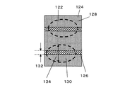
- FIG. 1A shows a structure of a conventional example
- FIGS. 1B and 1C conceptually show the structure of the present invention.
- the Si microcrystal 102 exists in the SiC polycrystal 104
- the boundary 106 of the microcrystal / polycrystal structure the potential confinement structure of the well and the barrier ,
- the boundary 106 of the two will coincide.
- the crystallinity of the well region is good, but the crystallinity is low at the boundary between the well and the barrier or at the barrier region.
- Si is an indirect transition type, it is necessary to reduce the potential confinement region to several nm, specifically about 4 nm or less, in order to greatly improve the light emission efficiency. If the well region is made small in order to carry out such small confinement, the wave function of electrons and holes cannot exist only in the well region, but it will increase to the barrier region.
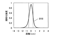
- FIG. 2A and 2B show examples of electron wave functions in the case of the Si quantum well structure.
- FIG. 2A shows a wave function 202 when the thickness of the Si quantum well is 1 nm and SiO 2 (8 eV) having a large band gap is used for the barrier layer. Even in such a large band gap, in the extremely thin region of 1 nm, for example, it has been clarified by the calculation of the inventors that the wave function oozes out to a part of the barrier region (about 1 nm).
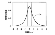
- FIG. 2B shows a wave function 204 in the case where SiC, which is a semiconductor material capable of passing a current, is similarly used for the barrier region, and the thickness of the Si quantum well is 1 nm.
- the band gap is smaller than that of SiO 2 and the potential barrier is also reduced, it is clear that the amount of the wave function that oozes out to the barrier region is further increased (about 3 nm). In this case, the probability that electrons and holes are present in the barrier layer cannot be ignored, and as a result, the rate of recombination in the barrier layer also increases. At this time, reflecting the low crystallinity of the barrier layer, non-radiative recombination with a high recombination rate occurs preferentially, and as a result, the luminous efficiency of the entire light emitting layer is greatly reduced. Even though it is possible to control the size of the microcrystals on average, it is extremely difficult to make all the microcrystals the same size, and the emission spectrum from the microcrystals has a large distribution. As a result, the half width increases.
- the present invention provides a light-emitting element that can improve the light-emitting efficiency of a light-emitting layer formed using a group IV semiconductor material and can obtain a light emission spectrum in a narrow band, and a method for manufacturing the light-emitting element. For the purpose of provision.
- the light-emitting device of the present invention is a light-emitting device having a light-emitting layer having a potential confinement structure including a well region and a barrier region adjacent to the well region, which are made of different group IV semiconductor materials, and the well in the light-emitting layer.
- a continuous region extending from a region to a part of the barrier region beyond the interface between the well region and the barrier region is formed by microcrystals, and the region other than the region formed by the microcrystals in the barrier region
- the region is formed by an amorphous or polycrystalline region.
- the light emitting device manufacturing method of the present invention is a method of manufacturing a light emitting device having a light emitting layer having a potential confinement structure including a well region and a barrier region, which are made of different group IV semiconductor materials, and includes the well region and the well region.
- a first step of forming a microcrystal in the well region, and passing the microcrystal beyond the interface between the well region and the barrier region And a second step of growing into a part of the region.
- the light emitting element which can improve the light emission efficiency of the light emitting layer formed using group IV semiconductor material, and can obtain the light emission spectrum of a narrow zone
- the barrier layer is a diagram illustrating the wave function in the Si quantum wells in the case of using SiO 2. It is a figure explaining the wave function in Si quantum well at the time of using SiC for a barrier layer. It is a cross-sectional schematic diagram of the light emitting element of Example 1 of the present invention. It is a cross-sectional schematic diagram of the light emitting layer of Example 1 of this invention. It is a figure explaining the sequence which forms the light emitting layer in Example 1 of this invention.
- the present invention is based on the knowledge that the following structure is effective for improving the light emission efficiency of a light emitting element having a light emitting layer having a confinement structure having a well region of about several nm. It was discovered. That is, in order to improve the light emission efficiency in such a structure, not only the well region but also a region where electrons and holes may exist outside the well region, that is, a barrier region adjacent to the well region, has high crystallinity. It is based on the knowledge that it is effective to have These will be described with reference to FIGS. 1A to 1D which are shown for explaining the comparison between the present invention and the conventional example.
- FIG. 1B shows a quantum well structure formed of a group IV semiconductor material
- FIG. 1C shows a quantum dot structure.
- Si x Ge y C (1-xy) can be used as the group IV semiconductor material. Both are composed of a microcrystalline region 122 and an amorphous or polycrystalline region 124 from the viewpoint of crystal, and are composed of a Si quantum well region 126 and a SiC barrier region 128 from the viewpoint of potential confinement.
- the microcrystalline region (inside the dotted line) 122 extends not only to the Si quantum well region 126 but also to a part 130 of the adjacent barrier region.
- the length 132 of the well region in the direction in which the potential confinement is performed is preferably shorter than the length 134 of the microcrystal in the same confinement direction.
- the length 134 of the microcrystal is three times or more the length 132 of the well region. Therefore, even if the wave function greatly spreads to the barrier region due to confinement by an extremely small well region, it is possible to maintain high luminous efficiency reflecting good crystallinity. In this structure, it is preferable that the center of the microcrystal exists in the well region.
- the band gap of the material of the barrier region is preferably 3 eV or less.
- sufficient conductivity is generated in the barrier region, and carriers can be injected from the barrier region to the well region.
- the wave function tends to ooze out in the barrier region, and the present invention functions more effectively. That is, it becomes possible to achieve both effective potential confinement and sufficient current injection.
- the crystallite size and the potential confinement size can be controlled separately, an emission spectrum with a narrow half-value width can be obtained almost without being affected by the microcrystal size variation that occurs during formation.
- the degree of demand for microcrystal size control from the viewpoint of wavelength control is relaxed, the conditions of process steps in element formation are widened, and element formation with a high yield is also possible.
- a microcrystal including a barrier region adjacent to a well region continuously is used for a light emitting layer. It is also important to be able to form this structure by growing microcrystals beyond the interface between the well region and the barrier region and into a part of the barrier region. That is, in order to form this structure, a two-step process including the first process and the second process in (1) and (2) as described below is important. (1) As a first step, a crystallite or a crystallite nucleus is formed in the well region. (2) As a second step, the crystallites are continuously grown up to the barrier region. This may be performed simultaneously with the formation of the layer structure, or may be performed after the formation of the layer structure once.
- the layer structure may be formed so that more or larger microcrystalline nuclei and microcrystalline regions are formed in the well region and the barrier region adjacent thereto.
- plasma CVD plasma enhanced chemical vapor deposition
- annealing may be performed with a laser having a wavelength that is absorbed only in the well region.
- a laser having a wavelength that is absorbed only in the well region.
- a desired microcrystal is formed by two-step annealing.
- the first annealing microcrystals are formed in the well region.
- the microcrystal is grown so that the microcrystalline region in the well region reaches the barrier region beyond the well / barrier interface by the second annealing.
- a temperature at which microcrystals are formed in the well region but microcrystals are not formed in the barrier region is used.
- a temperature for microcrystallization only in the well may be performed using a laser having a wavelength that does not absorb in the barrier region but absorbs only in the well region. In this case, if the laser is irradiated continuously in time, the heat generated by absorption expands to the barrier region, so that only the well region is annealed by performing a short pulse irradiation that does not diffuse the heat to the barrier region. Is desirable.
- the temperature required for microcrystallizing the well region that is, the first time is used.
- a higher temperature is required However, it can be lower than the temperature at which microcrystals are formed only in the barrier region. By using such a temperature, it is possible to continuously crystallize from the microcrystal existing in the well region to the barrier region.
- by performing annealing using a laser having a shorter wavelength than the laser used for the first time it is possible to expand the microcrystal to the barrier region using the microcrystal existing in the well region as a nucleus.
- the crystal structures of the well region and the barrier region need to be the same or similar.
- both the well region and the barrier region are group IV semiconductor materials and are of a diamond type, a zinc zinc type, or a wurtzite type. It is possible to apply the present invention to the group IV semiconductor using a material containing a small amount of different elements such as boron, phosphorus, oxygen and nitrogen for the barrier region as long as the crystal structure is not changed.
- materials having completely different crystal structures such as SiO 2 and SiN are used for the barrier region, it is difficult to apply the present invention.
- a light emitting element having sufficient light emission efficiency can be formed even with an IV group semiconductor material that is an indirect transition. Also, light emission with a narrow emission spectrum can be obtained.
- Si has many various peripheral technologies such as electronic devices and MEMS. By integrating the technology and the light emitting element according to the present invention at the material level, it has great ripple effects such as high added value and low cost as a light source system. Can be expected.
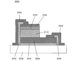
- Example 1 As Example 1, a configuration example of a light-emitting element using microcrystals using a Si-based material that is a group IV semiconductor to which the present invention is applied will be described with reference to FIGS. 3A and 3B.
- FIG. 3A is a schematic cross-sectional view of the light-emitting element 300 of this example
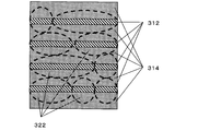
- FIG. 3B is a schematic cross-sectional view of the light-emitting layer 310 made of Si / SiC quantum well microcrystals constituting the light-emitting element 300.
- the light emitting element 300 of this example has an emission wavelength of 750 to 850 nm.
- the light emitting element 300 of this example is configured by the following layers.
- an Si driver substrate 302 on which a circuit for driving the light emitting element 300 is formed On an Si driver substrate 302 on which a circuit for driving the light emitting element 300 is formed, an insulating layer 304, an n-type SiC microcrystalline layer 306, a light emitting layer 310, a p-type SiC microcrystalline layer 330, a p-type Si contact layer 332, These layers are laminated.
- the light emitting layer 310 has a multiple quantum well structure including a Si quantum well layer 312 of about 1 nm and a SiC barrier layer 314 of about 10 nm.
- the light-emitting layer 310 has a potential confinement structure made of Si and SiC using different group IV semiconductor materials.
- a region closed by a dotted line is a microcrystalline region 322.
- the other regions are amorphous or polycrystalline here.
- the length of this microcrystal is about 10 nm in the stacking direction of the wells that are confined. In the in-plane direction of the well, it is the same or larger value.
- the microcrystals in the p-type SiC microcrystal layer 330 and the n-type SiC microcrystal layer 306 are larger than the microcrystals in the light-emitting layer and are several tens of nm to several ⁇ m, and have characteristics suitable as a doping layer and further as a pn junction. It is the size that can be obtained. Also, an insulating layer 340, an n-side electrode 342, and a p-side electrode 344 are formed for current injection. The electrode is directly connected to the circuit in the Si driver substrate by patterning so that the light emitting element can be driven by the Si driver.
- the band gap is 2.2 eV, which is smaller than 3 eV, and the center of the microcrystal exists in the well region.
- the length of the microcrystal in the confinement direction is longer than the length of the well region, and the length of the microcrystal is more than three times the length of the well region.
- the size of the microcrystal is not uniform, but the emission wavelength depends on the Si / SiC quantum well structure that is potential confinement, and does not depend on the size of the microcrystal. An emission spectrum having the same emission wavelength from the microcrystal and a narrow half width can be obtained.
- a method for manufacturing the light emitting device 300 in this example will be described.
- a method of forming microcrystals in the well region and growing it to the barrier region at the same time in the step of stacking the well region and the barrier region is used.
- an n-type SiC microcrystalline layer 306 capable of obtaining desired characteristics is formed by plasma CVD on the Si driver substrate 302 covered with the insulating layer 304.
- SiH 4 is used as the Si material
- C 3 H 8 is used as the C material
- PH 3 diluted to 3% is used as the dopant.
- H 2 is introduced so that microcrystals can be obtained.
- the substrate temperature is 200 to 400 ° C. This temperature is also a temperature that does not damage the Si driver.
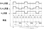
- FIG. 4 shows the correspondence between the structure and the gas flow rate with respect to the elapsed time as a sequence for formation.
- a time region for forming a Si quantum well layer and a SiC barrier layer and a time region for forming an amorphous or microcrystal are shown.
- gas flow rates changes in SiH 4 , C 3 H 8 and H 2 flow rates with respect to elapsed time are shown.
- a SiC barrier layer is formed to 7 nm with a small H 2 flow rate.
- the SiC barrier layer is formed to 3 nm by increasing the flow rate of H 2 by about 10 times.
- both the Si quantum well layer and the SiC barrier layer are formed under conditions with a high hydrogen flow rate, microcrystal formation and microcrystal expansion occur randomly. That is, as shown in FIG. 1D, a high proportion of the microcrystalline region 122 whose center does not exist in the well layer is formed, and the amorphous or polycrystalline region 124 or the microcrystalline region 122 and the amorphous or polycrystalline region 124 are formed in the well layer. A microcrystalline region having many interfaces is formed. Therefore, a situation occurs in which the luminous efficiency is not improved. Therefore, a desired light emitting layer structure 310 as shown in FIG. 3B is obtained only by modulating an appropriate H 2 flow rate according to the well / barrier structure as shown in FIG. After the light emitting layer is formed, the p-type SiC microcrystalline layer 330 and the p-type Si contact layer 332 are subsequently formed. B 2 H 6 diluted to 3% is used as the dopant.
- annealing may be performed in order to improve the crystallinity of the formed microcrystal.
- annealing may be performed using a laser having a wavelength that is absorbed only in the well region.
- the n layer is exposed, the insulating layer 340 is deposited, and the n-side electrode 342 and the p-side electrode 344 are formed, and the element 300 capable of current injection is manufactured.
- Si is used for the well region and SiC is used for the barrier region, but any combination of group IV semiconductors capable of potential confinement, that is, having different band gaps may be used. Further, as long as the crystal structure (diamond type, zinc-blende type or wurtzite type) of the IV group semiconductor material does not change, elements other than the IV group, for example, boron, phosphorus, oxygen and nitrogen may be contained.
- Example 2 As Example 2, a configuration example of a light-emitting element using microcrystals using a Si-based material that is a group IV semiconductor having a different form from Example 1 will be described with reference to FIGS. 5A to 5C.
- FIG. 5A is a schematic cross-sectional view of the light-emitting element 500 of this example
- FIG. 5B is a schematic cross-sectional view of the light-emitting layer 510 formed of Si / SiC quantum dot microcrystals constituting the light-emitting element 500.
- the light emitting element 500 of this example has an emission wavelength of 650 to 700 nm.
- the light emitting element 500 of this example is configured by the following layers.
- a p-type SiC microcrystalline layer 506, a light emitting layer 510, an n-type SiC microcrystalline layer 530, and an n-type Si contact layer 532 are stacked on a p-type Si substrate 502.
- the light emitting layer 510 has a multi-quantum dot structure composed of a Si quantum dot 512 of about 2 nm and a SiC barrier region 514 of about 10 nm or more.
- a potential confinement structure is formed by the Si quantum dots 512 and the SiC barrier region 514.
- regions 522 and 524 closed by dotted lines are microcrystalline regions. The other regions here are amorphous or polycrystalline.
- the size of the microcrystalline region 522 is about 10 nm.
- the size of the well region is 2 nm.
- a region 524 having a size of about 20 nm also exists across two quantum wells.
- the crystallites of the p-type SiC microcrystal layer 506 and the n-type SiC microcrystal layer 530 are several tens of nanometers to several ⁇ m in size, which is larger than the microcrystal of the light emitting layer, and have characteristics suitable as a doping layer and further as a pn junction. It is the size that can be obtained. Also, an insulating layer 540, a p-side electrode 542, and an n-side electrode 544 are formed for current injection. In order to prevent unnecessary current diffusion inside the device, the light emitting layer 510, the n-type SiC microcrystalline layer 530, and the n-type Si contact layer 532 may be etched into a post shape to confine the current.
- an electrode pad of about 100 ⁇ m square is provided in a region sufficiently away from the light emitting region in order to perform wiring by wire bonding or the like.
- the material of the barrier region is zincblende SiC
- the band gap is 2.2 eV, which is smaller than 3 eV
- the length of the microcrystal in the confinement direction is longer than the length of the well region.
- a method for manufacturing the light emitting element 500 will be described.
- a method is used in which after the well region and the barrier region are stacked, microcrystals are formed in the well region and grown to the barrier region.
- a p-type SiC microcrystalline layer 506 capable of obtaining desired characteristics is formed on a p-type Si substrate 502 by plasma CVD.
- SiH 4 is used as the Si raw material
- C 3 H 8 is used as the C raw material
- B 2 H 6 diluted to 3% is used as the dopant.
- hydrogen is introduced so that microcrystals can be obtained.
- the substrate temperature is 300 to 700 ° C.
- a layer structure 550 (FIG.
- the SiH 4 flow rate and the C 3 H 8 flow rate are adjusted so that the Si X C1- X layer 552 has a Si content larger than that of the SiC layer 554 with x being larger than 0.5. Specifically, the SiH 4 / C 3 H 8 supply ratio is increased.
- an n-type SiC microcrystalline layer 530 and an n-type Si contact layer 532 are subsequently formed.
- PH 3 diluted to 3% is used as a dopant.
- annealing is performed at 500 to 700 ° C. in a hydrogen atmosphere for 30 minutes.
- Si x C 1-y layer 552 since the Si x C 1-y layer 552 has a large Si content, it is phase-separated into Si and SiC, and Si quantum dots 512 having a uniform particle size of about 2 nm are formed.
- a SiC barrier region is formed around the dot. If the Si content is too large, a structure close to the Si quantum well is formed. If the Si content is too small, a structure close to the SiC barrier is formed, so that an appropriate Si content is required.
- the Si quantum dots 512 formed by phase separation are formed as microcrystals.
- the SiC region formed by phase separation and the originally existing SiC barrier layer 554 remain amorphous or become polycrystalline because of the low temperature.
- annealing is performed at 700 to 1000 ° C. in a hydrogen atmosphere for 30 minutes.
- the SiC region 526 around the Si quantum dots 512 that is, even a part of the 10 nm SiC layer 554 is continuously microcrystallized from the Si quantum dots 512 to form the microcrystal regions 522.
- a temperature lower than the temperature at which SiC is microcrystallized alone is used, microcrystallization hardly occurs only in the region of 10 nm SiC layer 554.
- a post shape is formed, an insulating film 540 is deposited, and an n-side electrode 544 and a p-side electrode 542 are formed, and an element capable of current injection is manufactured.
- materials Si is used for the well region and SiC is used for the barrier region, but any combination of group IV semiconductors capable of potential confinement, that is, having different band gaps may be used.
- the crystal structure (diamond type, zinc-blende type or wurtzite type) of the group IV semiconductor material does not change, elements other than group IV, for example, boron, phosphorus, oxygen and nitrogen may be contained.
- Example 3 As Example 3, a configuration example of a light-emitting element using microcrystals using a Si-based material that is a group IV semiconductor having a different form from those of Example 1 and Example 2 will be described with reference to FIGS. 6A and 6B.
- FIG. 6A is a schematic cross-sectional view of the light-emitting element 600 of this example
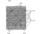
- FIG. 6B is a schematic cross-sectional view of the light-emitting layer 610 made of Si / SiC quantum dot microcrystals constituting the light-emitting element 600.
- the light emitting element 600 of this example has an emission wavelength of 950 to 1050 nm.
- description of the same configurations as those of the first and second embodiments will be omitted.
- FIG. 6A shows a light emitting element structure including a light emitting layer 610 on a glass substrate 602.
- the light emitting layer 610 has a multiple quantum well structure composed of a SiGe quantum well layer 612 of about 1 nm and a SiC barrier layer 614 of about 10 nm.
- a potential confinement structure is formed by the SiGe quantum well layer and the SiC barrier layer. Others are the same as in the first embodiment.
- regions 622 and 624 closed by dotted lines are microcrystalline regions. Other areas are amorphous here.
- the length of the microcrystal is about 10 nm in the well stacking direction in which confinement is performed. The value is larger in the in-plane direction of the well.
- a microcrystal 624 having a size of about 20 nm also exists across two quantum wells.
- the p-layer and n-layer microcrystals are larger than the light-emitting layer microcrystals by several tens of nanometers to several ⁇ m, and are sized to obtain characteristics suitable as a doping layer and further as a pn junction. .
- an insulating layer, a p-side electrode 644 and an n-side electrode 642 are formed for current injection.
- the light emitting layer 610, the p-type SiC microcrystalline layer, and the p-type Si contact layer may be etched into a post shape to confine the current.
- an electrode pad of about 100 ⁇ m square is provided in a region sufficiently away from the light emitting region in order to perform wiring by wire bonding or the like.
- the material of the barrier region is zincblende SiC
- the band gap is 2.2 eV, smaller than 3 eV
- the wavelength at which absorption begins to occur is 560 nm or more.
- the SiGe quantum well has a transition energy of about 1.2 eV and an emission wavelength of about 1 ⁇ m.
- the length of the microcrystal in the confinement direction is longer than the length of the well region, and the length of the microcrystal is more than three times the length of the well region.
- the size of the microcrystal is non-uniform, but the emission wavelength depends on the SiGe / SiC quantum well structure and does not depend on the size of the microcrystal. Can also obtain an emission spectrum having the same half width.
- a method for manufacturing the light emitting device of this example will be described.
- a method is used in which after the well region and the barrier region are stacked, microcrystals are formed in the well region and grown to the barrier region.
- an n-type SiC microcrystalline layer capable of obtaining desired characteristics is formed on the glass substrate 602 by plasma CVD.
- SiH 4 is used as the Si material
- C 3 H 8 is used as the C material
- PH 3 diluted to 3% is used as the dopant.
- hydrogen is introduced so that microcrystals can be obtained.
- the substrate temperature is 200 to 400 ° C.
- a light emitting layer 610 having a SiGe / SiC quantum well structure is formed.
- About 1 nm of SiGe amorphous layers 612 and about 10 nm of SiC amorphous layers 614 are alternately deposited by plasma CVD.
- the SiGe amorphous layer 612 is formed by supplying SiH 4 and GeH 4
- the SiC amorphous layer 614 is formed by supplying SiH 4 and C 3 H 8 . It may be supplied with H 2 as necessary.
- a p-type SiC microcrystalline layer and a p-type Si contact layer are subsequently formed. B 2 H 6 diluted to 3% is used as the dopant.
- annealing is performed by scanning on a wafer using a titanium sapphire laser having a wavelength of 800 nm and a pulse width of several nsec as the first time.
- a titanium sapphire laser having a wavelength of 800 nm and a pulse width of several nsec as the first time.
- the SiC barrier layer 614 uses a wavelength that does not cause direct absorption, the temperature rise is suppressed and microcrystallization of this layer hardly occurs.
- annealing is performed by scanning on the wafer using an excimer laser having a wavelength of about 350 nm and a pulse width of several nsec.
- a part 626 of the SiC barrier layer around the SiGe quantum well layer 612 is continuously microcrystallized from the SiGe quantum well 612 to form a microcrystalline region 622.
- the intensity lower than the laser intensity at which SiC is microcrystallized by itself is used, microcrystallization of only the region of SiC layer 614 of about 10 nm hardly occurs.
- a post shape is formed, an insulating film is deposited, and an n-side electrode 642 and a p-side electrode 644 are formed to produce an element capable of current injection.
- SiGe is used for the well region and SiC is used for the barrier region, but any combination of IV group semiconductors capable of potential confinement, that is, having different band gaps may be used.
- elements other than the IV group for example, boron, phosphorus, oxygen and nitrogen may be contained.
- the structure of the present invention and the manufacturing method thereof are not limited at all by the configuration examples described in each of the above-described embodiments, and are in accordance with the gist of the present invention. As long as it is, the thing by the combination which is not demonstrated above is also contained in this invention.
- 300 light emitting element 302: Si driver substrate 304: insulating layer 306: n-type SiC microcrystalline layer 310: light emitting layer 312: Si quantum well layer 314: SiC barrier layer 322: microcrystalline region 330: p-type SiC microcrystalline layer 332 : P-type Si contact layer 340: insulating layer 342: n-side electrode 344: p-side electrode
Landscapes
- Led Devices (AREA)
Abstract
IV族半導体材料を用いて形成された発光層の発光効率を向上させることができ、狭い帯域の発光スペクトルを得ることが可能となる発光素子及びその製造方法を提供する。異なるIV族半導体材料からなる、井戸領域と該井戸領域に隣接するバリア領域とを備えたポテンシャル閉じ込め構造の発光層を有する発光素子であって、前記発光層における前記井戸領域から、該井戸領域と前記バリア領域との界面を越えた該バリア領域の一部に亙る連続した領域が、微結晶によって形成され、前記バリア領域における前記微結晶によって形成されている領域以外の領域が、アモルファスまたは多結晶領域によって形成されている。
Description
本発明は、発光素子及びその製造方法に関し、特にIV族半導体材料を用いて形成された発光層を備えた発光素子及びその製造方法に関する。
現在、半導体発光素子のほとんどはIII-V族化合物半導体材料を用いて形成されている。 これはIII-V族化合物半導体が、直接遷移型のバンド構造を持ち、室温においても高い発光効率が得られるからである。 一方、Siなどの間接遷移型のバンド構造をもつ材料では、発光効率が極めて低く、発光素子材料としては適していないというのが通説であった。 近年、このSiなどの間接遷移型のバンド構造をもつ材料であっても、電子とホールを数nmの狭い領域に閉じ込めることで、光を発生する発光再結合の確率を高めて、発光素子へ応用する試みがなされている。 このように数nmの領域に電子やホールを閉じ込めるには、大きなポテンシャル障壁(例えば300meV以上)による閉じ込め構造が必要で、バンドギャップが大きく異なる材料同士のヘテロ接合が必須となる。 III-V族化合物半導体では、格子整合しつつ、すなわち良質な単結晶層の積層に基づく、バンドギャップが大きく異なる材料のヘテロ接合を形成することが可能である。 例えば、GaAs/AlGaAsなどが挙げられる。そのヘテロ接合により、量子井戸や量子ドットを形成してポテンシャル障壁に囲まれた閉じ込め領域(例えば、井戸やドット)を形成し、そこに電子とホールを閉じ込めることが可能となっている。
一方、IV族半導体であるSi系材料では、バンドギャップが大きく異なり、かつ格子整合する材料が存在しない。 例えば、Si(バンドギャップ:1.1eV、格子定数:5.4309Å)よりもバンドギャップが十分大きなSiC(バンドギャップ:2.2~2.9eV、格子定数:4.3596Å)は格子不整合が約20%もあり、単結晶層同士のヘテロ接合による良質なポテンシャル閉じ込め領域を形成することは極めて困難な状況となっている。 他方、IV族半導体では上記格子整合条件を緩和させるために、構造柔軟性が高いアモルファスまたは多結晶などの構造体でヘテロ接合を形成する試みも、太陽電池応用などに向けて試みられている。 この場合、太陽電池のように受光素子としては機能するものの、アモルファスまたは多結晶体に多く存在する非発光再結合センターによる再結合の影響で、発光素子としては十分な効率を稼ぐことができない。
そこで、Si系材料などでポテンシャル閉じ込め領域を形成する手法の一つとして、数nmのサイズの微結晶をアモルファスあるいは多結晶領域内に形成する手法が提案されている。 この方法では、アモルファスや多結晶などの構造柔軟性をもつ構造体内に良質な微結晶を形成し、この微結晶領域では内部に欠陥や不純物などの非発光再結合センターになり得るものが存在しない領域を形成する方法である。 この狭い微結晶領域に電子とホールを閉じ込めることにより非発光再結合が抑制され、さらに、電子とホールの波動関数の重なりが大きくなることから発光再結合が促進される。この二つの効果により、間接遷移型のバンド構造をもつ材料であっても発光効率を高めることが可能になってきている。 さらに、この場合、電子やホールが数nmの領域に閉じ込められるため、その発光波長は、量子サイズ効果により、閉じ込めが存在しない場合に比較して短波長化する。したがって、微結晶の大きさが制御できれば発光波長の設計・制御も可能になる。
このような手法によるものとして、特許文献1ではSi微結晶とSiC多結晶体を用いた発光素子やその形成方法が提案されている。 この特許文献1での発光素子は、粒径がナノメートルオーダのSiまたはGe微結晶がSiC多結晶体中にドット状に分散した発光層を持つように構成されている。 また、その形成方法は、減圧化学気相堆積法などで、SiC多結晶膜とSiまたはGe微結晶を交互に堆積して形成される。または、SiC多結晶膜とSiまたはGe多結晶膜を交互に形成した後に、真空中などでアニール処理してSiまたはGe微結晶を形成する手法が採られている。
上記従来例の特許文献1のものにおいては、つぎのような課題を有している。これを、本発明と従来例との比較を説明するために示されている図1Aから1Dを用いて説明する。 図1Aから1Dにおいて、図1Aは従来例の構造を示すものであり、図1B、Cは本発明の構造を概念的に示したものである。 上記従来例の構造では、図1Aに示すように、Si微結晶102がSiC多結晶体104内に存在することから、微結晶と多結晶という構造体の境界106と井戸とバリアというポテンシャル閉じ込め構造の境界106が一致することになる。 すなわち、井戸領域の結晶性は良好であるが、井戸とバリアとの境界やバリア領域では結晶性が低いことを意味する。 ここで、Siは間接遷移型であるために、発光効率を大きく向上させるためには、ポテンシャル閉じ込め領域を数nm、具体的には4nm以下程度まで小さくする必要がある。 このような小さな閉じ込めを行うために、井戸領域を小さくすると、電子やホールの波動関数は井戸領域だけに存在できずバリア領域にまで大きくしみだす。
図2Aと2BにSi量子井戸構造の場合の電子の波動関数の例を示す。 図2AにSi量子井戸の厚さが1nmで、バリア層にバンドギャップの大きなSiO2(8eV)を用いた場合の波動関数202を示す。 このような大きなバンドギャップであっても、例えば1nmといった極めて薄い領域では、バリア領域の一部(約1nm)まで波動関数がしみだす様子が発明者らの計算により解明されている。 図2Bに、同じくSi量子井戸の厚さが1nmで、電流を流すことができる半導体材料であるSiCをバリア領域に用いた場合の波動関数204を示す。 この場合、バンドギャップがSiO2に比べ小さくなりポテンシャル障壁も小さくなるため、波動関数のバリア領域へのしみ出し量はさらに大きくなる(約3nm)ことも明らかである。 この場合、電子やホールがバリア層に存在する確率も無視できなくなり、その結果、バリア層で再結合する割合も増大する。 その際に、バリア層の低い結晶性を反映して、再結合速度の速い非発光再結合が優先的に起こり、その結果、発光層全体としての発光効率が大きく低下してしまうこととなる。 また、微結晶の大きさを平均的に制御することは可能であっても、全ての微結晶の大きさを同一に揃えることは極めて難しく、微結晶からの発光スペクトルは大きな分布をもち、その結果、半値幅が増大することとなる。
本発明は、上記課題に鑑み、IV族半導体材料を用いて形成された発光層の発光効率を向上させることができ、狭い帯域の発光スペクトルを得ることが可能となる発光素子及びその製造方法の提供を目的とする。
本発明の発光素子は、異なるIV族半導体材料からなる、井戸領域と該井戸領域に隣接するバリア領域とを備えたポテンシャル閉じ込め構造の発光層を有する発光素子であって、前記発光層における前記井戸領域から、該井戸領域と前記バリア領域との界面を越えた該バリア領域の一部に亙る連続した領域が、微結晶によって形成され、前記バリア領域における前記微結晶によって形成されている領域以外の領域が、アモルファスまたは多結晶領域によって形成されていることを特徴とする。 また、本発明の発光素子製造方法は、異なるIV族半導体材料からなる、井戸領域とバリア領域とを備えたポテンシャル閉じ込め構造の発光層を有する発光素子の製造方法であって、前記井戸領域と該井戸領域に隣接するバリア領域とによる層構造を形成するに当たり、前記井戸領域内に微結晶を形成する第1の工程と、前記微結晶を井戸領域とバリア領域の界面を越えて該バリア領域の一部の領域内まで成長させる第2の工程と、を有することを特徴とするとする。
本発明によれば、IV族半導体材料を用いて形成された発光層の発光効率を向上させることができ、狭い帯域の発光スペクトルを得ることが可能となる発光素子及びその製造方法を実現することができる。
つぎに本発明の実施形態におけるIV族半導体であるSi系材料を用いて形成された発光層を備えた発光素子の構成例について説明する。
本発明は、数nm程度の井戸領域をもつ閉じ込め構造の発光層を備えた発光素子での発光効率を向上させるためには、つぎのような構造とすることが有効であるとの知見に基づいて見出されたものである。 すなわち、このような構造において発光効率を向上させるためには、井戸領域だけでなく、井戸領域外側で電子やホールが存在する可能性のある領域、すなわち井戸領域に隣接したバリア領域まで高い結晶性をもつことが有効であるとの知見に基づくものである。 これらを、本発明と従来例との比較を説明するために示されている図1Aから1Dを用いて説明する。 図1BはIV族半導体材料で形成した量子井戸構造であり、図1Cは量子ドット構造である。本実施例では、このIV族半導体材料としてSixGeyC(1-x-y)を用いることができる。 いずれも、結晶の観点では微結晶領域122とアモルファスまたは多結晶領域124で構成され、ポテンシャル閉じ込めの観点ではSi量子井戸領域126とSiCバリア領域128で構成されている。 ここで、微結晶領域(点線内部)122はSi量子井戸領域126にとどまらず、隣接したバリア領域の一部130まで大きく広がっている。 ポテンシャル閉じ込めがなされている方向における井戸領域の長さ132は、同じ閉じ込め方向における微結晶の長さ134より短いことが好ましい。 さらに、その微結晶の長さ134がその井戸領域の長さ132の3倍以上であることが望ましい。これにより、極めて小さい井戸領域による閉じ込めによって波動関数がバリア領域まで大きく広がっても、良好な結晶性を反映した高い発光効率を保つことができる。 この構造において、微結晶の中心が井戸領域内に存在する構造であることが好ましい。
さらに電流注入も可能にさせるために、バリア領域の材料のバンドギャップは3eV以下であることが望ましい。 この場合、バリア領域に十分な導電性が生じ、バリア領域から井戸領域へのキャリア注入が可能となる。このようなバンドギャップが比較的小さいバリア領域では波動関数はバリア領域により大きくしみだす傾向にあり、本発明がより有効に機能する形態である。 すなわち、効果的なポテンシャル閉じ込めと十分な電流注入を両立させることが可能となる。 また、本実施形態の構造では、微結晶サイズとポテンシャル閉じ込めサイズを別々に制御できることから、形成時に生じてしまう微結晶サイズばらつきの影響をほとんど受けず、半値幅の狭い発光スペクトルも得られる。 あるいは、波長制御の観点からの微結晶サイズ制御の要求度合いが緩和されるため、素子形成におけるプロセス工程の条件が広がり、歩留まりの高い素子形成も可能となる。
このように、井戸領域に隣接するバリア領域も連続的に含む微結晶を発光層に用いることが本発明の特徴である。また、微結晶を井戸領域とバリア領域の界面を越えてバリア領域の一部の領域内まで成長させこの構造が形成できる方法も重要である。 すなわち、この構造を形成するには、下記に示すような(1)と(2)における第1の工程と第2の工程とによる二段階の工程が重要である。
(1)第1の工程として、井戸領域内に微結晶、または微結晶の核となるものを形成する。
(2)第2の工程として、バリア領域まで連続的にその微結晶を成長させる。
これは、層構造形成時に同時に行ってもよいし、一旦層構造を形成し終えた後に行っても良い。 層構造形成時に同時に本発明の構造を作り込む場合、井戸領域およびそれに隣接したバリア領域で微結晶核や微結晶領域がより多くまたは大きく形成されるように層構造を形成すれば良い。 例えば、プラズマ化学気相堆積法(プラズマCVD)において微結晶を形成する際、導入水素量を大幅に増大させることで微結晶核やその領域の増大が可能になることが知られている。 そこで、前記井戸領域と、井戸領域に隣接する3nm幅のバリア領域の一部領域とを形成する際に、この一部領域以外のバリア領域を形成する際よりも水素流量を増やして形成すれば良い。
(1)第1の工程として、井戸領域内に微結晶、または微結晶の核となるものを形成する。
(2)第2の工程として、バリア領域まで連続的にその微結晶を成長させる。
これは、層構造形成時に同時に行ってもよいし、一旦層構造を形成し終えた後に行っても良い。 層構造形成時に同時に本発明の構造を作り込む場合、井戸領域およびそれに隣接したバリア領域で微結晶核や微結晶領域がより多くまたは大きく形成されるように層構造を形成すれば良い。 例えば、プラズマ化学気相堆積法(プラズマCVD)において微結晶を形成する際、導入水素量を大幅に増大させることで微結晶核やその領域の増大が可能になることが知られている。 そこで、前記井戸領域と、井戸領域に隣接する3nm幅のバリア領域の一部領域とを形成する際に、この一部領域以外のバリア領域を形成する際よりも水素流量を増やして形成すれば良い。
所望の微結晶の形成を確実にするために、上記形成後、井戸領域のみで吸収する波長を有するレーザでアニールしてもよい。 この方法では、井戸領域のみ選択的により加熱されるために、井戸領域を中心とした微結晶領域がより形成され易い。
一旦、層構造を形成した後に所望の微結晶を形成するには、二段階のアニールによって行う。 一回目のアニールでは、井戸領域内に微結晶を形成する。 続いて、二回目のアニールによって井戸領域内の微結晶領域が井戸・バリア界面を越えてバリア領域まで到達するように微結晶を成長させる。 一回目のアニールでは、井戸内にのみ選択的に微結晶を形成させるために、井戸領域で微結晶は形成されるが、バリア領域では微結晶が形成されない温度を用いる。 一般的にバンドギャップが大きい材料は原子の結合エネルギーが大きいために、結晶化させる(すなわち原子を最適な位置にまで動かす)にはより大きなエネルギー、すなわち温度が必要となる。ゆえに、上記のように井戸内のみ微結晶化させる温度が存在する。 あるいは、バリア領域では吸収せず井戸領域のみで吸収するような波長をもつレーザを用いて井戸のみのアニールを行っても良い。 この場合、レーザを時間的に連続照射すると吸収により発生した熱がバリア領域まで拡大してしまうため、バリア領域まで熱が拡散しない短時間のパルス照射を行うことで井戸領域のみのアニールを行うことが望ましい。
二回目の微結晶領域成長では、井戸領域に存在する微結晶を核としてその微結晶領域をバリア領域にまで成長させるため、井戸領域を微結晶化するのに必要な温度、すなわち一回目に用いた温度よりは高い温度が必要である。しかし、バリア領域だけに微結晶を形成する温度よりは低くすることができる。 そのような温度を用いることで井戸領域に存在する微結晶からバリア領域まで連続的に結晶化することが可能となる。 あるいは、一回目に用いたレーザよりも短波長のレーザを用いたアニールを行うことで井戸領域に存在する微結晶を核としてバリア領域まで微結晶を拡大させることが可能となる。 このように、バリア領域まで微結晶を連続的に成長させるためには、井戸領域とバリア領域の結晶構造が同一、もしくは類似している必要がある。 具体的には、井戸領域もバリア領域もIV族半導体材料であり、ダイヤモンド型、せん亜鉛型、またはウルツ鉱型であることが肝要である。 上記IV族半導体に、ボロン、りん、酸素や窒素などの異なる元素が少量含まれる材料をバリア領域に用いて本発明を適用することは、結晶構造が変わらない限り可能である。しかし、SiO2やSiNなど結晶構造が完全に異なる材料をバリア領域に用いた場合は、本発明を適用することは難しい。
以上の本実施形態の構成によれば、間接遷移であるIV族半導体材料であっても十分な発光効率をもつ発光素子が形成できる。 また、発光スペクトルの狭い発光が得られる。 さらに、Siは電子デバイスやMEMSなど多彩な周辺技術が多く、その技術と本発明による発光素子との材料レベルでの融合により、光源システムとしての高付加価値化や低コスト化など多大な波及効果を期待することができる。
以下に、本発明の実施例について説明する。
[実施例1]
実施例1として、本発明を適用したIV族半導体であるSi系材料を用いた微結晶による発光素子の構成例について、図3Aと3Bを用いて説明する。 図3Aは本実施例の発光素子300の断面模式図であり、図3Bは発光素子300を構成するSi/SiC量子井戸微結晶による発光層310の断面模式図である。 本実施例の発光素子300は、発光波長が750~850nmとされている。 また、本実施例の発光素子300は、つぎの各層によって構成されている。 発光素子300を駆動するための回路を形成したSiドライバー基板302上に、絶縁層304、n型SiC微結晶層306、発光層310、p型SiC微結晶層330、p型Siコンタクト層332、の各層が積層されて構成されている。
[実施例1]
実施例1として、本発明を適用したIV族半導体であるSi系材料を用いた微結晶による発光素子の構成例について、図3Aと3Bを用いて説明する。 図3Aは本実施例の発光素子300の断面模式図であり、図3Bは発光素子300を構成するSi/SiC量子井戸微結晶による発光層310の断面模式図である。 本実施例の発光素子300は、発光波長が750~850nmとされている。 また、本実施例の発光素子300は、つぎの各層によって構成されている。 発光素子300を駆動するための回路を形成したSiドライバー基板302上に、絶縁層304、n型SiC微結晶層306、発光層310、p型SiC微結晶層330、p型Siコンタクト層332、の各層が積層されて構成されている。
発光層310は、約1nmのSi量子井戸層312と、約10nmのSiCバリア層314とによる多重量子井戸構造を備えている。 そして、この発光層310は異なるIV族半導体材料によるSiとSiCとにより、ポテンシャル閉じ込め構造が形成されている。 一方、図3Bに示すように、点線で閉じられた領域が、微結晶領域322である。それ以外の領域は、ここではアモルファスまたは多結晶になっている。この微結晶の長さは、閉じ込めがなされている井戸の積層方向で約10nmである。井戸の面内方向ではそれと同等、もしくは、より大きな値となっている。
p型SiC微結晶層330およびn型SiC微結晶層306における微結晶は、サイズが発光層の微結晶よりも大きく数10nm~数μmあり、ドーピング層として、さらにはpn接合として適した特性が得られるようなサイズとなっている。 また、電流注入のために絶縁層340、n側電極342とp側電極344が形成されている。 電極はSiドライバー基板内の回路にパターニングにより直接接続され、Siドライバーによる発光素子の駆動が可能となるように構成されている。
本実施例の構造では、バリア領域の材料はせん亜鉛鉱型SiCが用いられ、バンドギャップは2.2eVであり、3eVより小さく、また、微結晶の中心は井戸領域内に存在する。 また、閉じ込め方向の微結晶の長さは、井戸領域の長さよりも長く、さらにその微結晶の長さは井戸領域の長さよりも3倍以上である。 また、本実施例の構造では、微結晶の大きさが不均一であるが、発光波長はポテンシャル閉じ込めであるSi/SiC量子井戸構造に依存し、微結晶の大きさには依存しないため、各微結晶からの発光波長は同一で半値幅の狭い発光スペクトルも得られる。
つぎに、本実施例における発光素子300の製造方法について説明する。
ここでは、井戸領域とバリア領域を積層する工程において同時に井戸領域内に微結晶を形成し、それをバリア領域まで成長させる方法を用いる。 まず、絶縁層304で覆われたSiドライバー基板302上に所望の特性が得られるようなn型SiC微結晶層306をプラズマCVDにより形成する。Si原料としてSiH4、C原料としてC3H8、またドーパントとして3%に希釈されたPH3を用いる。 さらに、H2を導入して微結晶が得られるようにする。基板温度は、200~400℃を用いる。この温度はSiドライバーにダメージを与えない温度にもなっている。 続いて、発光層を形成する。形成のためのシーケンスとして経過時間に対する構造と各ガス流量の対応を図4に示す。構造として、Si量子井戸層およびSiCバリア層を形成する時間領域と、アモルファスまたは微結晶を形成する時間領域を示してある。また、ガス流量として、経過時間に対するSiH4、C3H8およびH2流量の変化を示してある。 まず、SiCバリア層を少ないH2流量で7nm形成する。 その後、H2の流量を約10倍にしてSiCバリア層を3nm形成する。 このとき、SiH4およびC3H8の供給量を減らしてSiH4およびC3H8に対する相対的なH2量をさらに増大させている。 この後、C3H8の供給を停止し、SiH4とH2のみにしてSi量子井戸層を形成する。Si量子井戸層をそのまま1nm形成し終えたら、C3H8の供給を再開し、H2流量が多い状態のまま、3nmのSiC層を形成する。その後、H2流量を元の少ない流量に戻して、さらに、SiH4およびC3H8の流量も元の多い流量に戻して4nmのSiCバリア層を形成する。 以上でSi/SiC量子井戸微結晶構造が一組形成できたことになる。これを複数回繰り返すことによって、図3Bに示す310のような多重量子井戸微結晶を含む発光層が形成できる。
ここでは、井戸領域とバリア領域を積層する工程において同時に井戸領域内に微結晶を形成し、それをバリア領域まで成長させる方法を用いる。 まず、絶縁層304で覆われたSiドライバー基板302上に所望の特性が得られるようなn型SiC微結晶層306をプラズマCVDにより形成する。Si原料としてSiH4、C原料としてC3H8、またドーパントとして3%に希釈されたPH3を用いる。 さらに、H2を導入して微結晶が得られるようにする。基板温度は、200~400℃を用いる。この温度はSiドライバーにダメージを与えない温度にもなっている。 続いて、発光層を形成する。形成のためのシーケンスとして経過時間に対する構造と各ガス流量の対応を図4に示す。構造として、Si量子井戸層およびSiCバリア層を形成する時間領域と、アモルファスまたは微結晶を形成する時間領域を示してある。また、ガス流量として、経過時間に対するSiH4、C3H8およびH2流量の変化を示してある。 まず、SiCバリア層を少ないH2流量で7nm形成する。 その後、H2の流量を約10倍にしてSiCバリア層を3nm形成する。 このとき、SiH4およびC3H8の供給量を減らしてSiH4およびC3H8に対する相対的なH2量をさらに増大させている。 この後、C3H8の供給を停止し、SiH4とH2のみにしてSi量子井戸層を形成する。Si量子井戸層をそのまま1nm形成し終えたら、C3H8の供給を再開し、H2流量が多い状態のまま、3nmのSiC層を形成する。その後、H2流量を元の少ない流量に戻して、さらに、SiH4およびC3H8の流量も元の多い流量に戻して4nmのSiCバリア層を形成する。 以上でSi/SiC量子井戸微結晶構造が一組形成できたことになる。これを複数回繰り返すことによって、図3Bに示す310のような多重量子井戸微結晶を含む発光層が形成できる。
Si量子井戸層もSiCバリア層も全て水素流量の多い条件で形成すると、微結晶形成および微結晶拡大がランダムに起こる。 つまり、図1Dのように中心が井戸層に存在しない微結晶領域122が高い割合で形成され、井戸層内にアモルファスまたは多結晶領域124、または微結晶領域122とアモルファスまたは多結晶領域124との界面が多く存在するような微結晶領域が形成されてしまう。よって発光効率が改善されない状況が生じる。 したがって、図4に示すような井戸・バリア構造に応じた適切なH2流量などの変調を行うことで初めて図3Bに示す310のような所望の発光層の構造が得られる。 発光層形成後、p型SiC微結晶層330およびp型Siコンタクト層332を引き続き形成する。ドーパントとして3%に希釈されたB2H6を用いる。
以上で層構造の形成が終了する。 ここで、形成された微結晶の結晶性を向上させるために、アニールを行ってもよい。 井戸領域内に多く存在する微結晶を選択的にアニールするために、井戸領域でのみ吸収する波長をもつレーザを用いてアニールしても良い。 続いて、良く知られた半導体プロセス技術を用いて、n層の露出、絶縁層340の堆積、n側電極342およびp側電極344の形成を行い、電流注入可能な素子300が作製される。 ここで材料として、井戸領域にSiを、バリア領域にSiCを用いているが、ポテンシャル閉じ込めが可能な、つまりバンドギャップが異なるIV族半導体の組み合せであれば良い。 また、IV族半導体材料においてその結晶構造(ダイヤモンド型、せん亜鉛鉱型やウルツ鉱型)が変わらない限り、IV族でない元素、例えば、ボロン、りん、酸素や窒素が入っていても構わない。
[実施例2]
実施例2として、実施例1と異なる形態のIV族半導体であるSi系材料を用いた微結晶による発光素子の構成例について、図5Aから5Cを用いて説明する。 図5Aは本実施例の発光素子500の断面模式図であり、図5Bは発光素子500を構成するSi/SiC量子ドット微結晶による発光層510の断面模式図である。 本実施例の発光素子500は、発光波長が650~700nmとされている。 また、本実施例の発光素子500は、つぎの各層によって構成されている。 p型Si基板502上に、p型SiC微結晶層506、発光層510、n型SiC微結晶層530、n型Siコンタクト層532、の各層が積層されて構成されている。
実施例2として、実施例1と異なる形態のIV族半導体であるSi系材料を用いた微結晶による発光素子の構成例について、図5Aから5Cを用いて説明する。 図5Aは本実施例の発光素子500の断面模式図であり、図5Bは発光素子500を構成するSi/SiC量子ドット微結晶による発光層510の断面模式図である。 本実施例の発光素子500は、発光波長が650~700nmとされている。 また、本実施例の発光素子500は、つぎの各層によって構成されている。 p型Si基板502上に、p型SiC微結晶層506、発光層510、n型SiC微結晶層530、n型Siコンタクト層532、の各層が積層されて構成されている。
発光層510は約2nmのSi量子ドット512と約10nm以上のSiCバリア領域514からなる多重量子ドット構造である。このSi量子ドット512とSiCバリア領域514によりポテンシャル閉じ込め構造が形成されている。 一方、図5Bに示すように点線で閉じられた領域522および524が、微結晶の領域である。それ以外の領域はここではアモルファスまたは多結晶になっている。この微結晶領域522の大きさは、約10nm程度である。 井戸領域の大きさは2nmである。また、一部二つの量子井戸を跨いで、20nm程度の大きさの領域524も存在する。
p型SiC微結晶層506およびn型SiC微結晶層530の微結晶は、サイズが発光層の微結晶よりも大きい数10nm~数μmあり、ドーピング層として、さらにはpn接合として適した特性が得られるようなサイズとなっている。 また、電流注入のために絶縁層540、p側電極542とn側電極544が形成されている。 素子内部における不必要な電流の拡散を防ぐために、発光層510、n型SiC微結晶層530、n型Siコンタクト層532をポスト状にエッチングし、電流狭窄してもよい。素子表面にあるn側電極544ではワイヤーボンディングなどによる配線を行うために、100μm角程度の電極パッドを発光領域から十分離れた領域に設けてある。本実施例の構造では、バリア領域の材料はせん亜鉛鉱型SiCでバンドギャップは2.2eVであり、3eVより小さく、また閉じ込め方向の微結晶の長さは、井戸領域の長さよりも長い。
つぎに、本発光素子500の製造方法について説明する。 ここでは、井戸領域とバリア領域とを積層した後に井戸領域内に微結晶を形成し、それをバリア領域まで成長させる方法を用いる。 まず、p型Si基板502上に所望の特性が得られるようなp型SiC微結晶層506をプラズマCVDにより形成する。 Si原料としてSiH4、C原料としてC3H8、またドーパントとして3%に希釈されたB2H6を用いる。 さらに、水素を導入して微結晶が得られるようにする。基板温度は、300~700℃を用いる。 続いて、発光層510を形成するための層構造550(図5C)を形成する。 この層構造550は約2nmのSiXC1-Xアモルファス層552と約10nmのSiCアモルファス層554をプラズマCVDにて交互に堆積する。ここで、SiXC1-X層552は、xは0.5より大きくSiC層554よりもSi含有量が多くなるように、形成時のSiH4流量とC3H8流量を調整する。具体的には、SiH4/C3H8供給比を大きくする。
層構造550を形成後、n型SiC微結晶層530およびn型Siコンタクト層532を引き続き形成する。 ドーパントとして3%に希釈されたPH3を用いる。
以上、層構造全体の形成が終了して、引き続き発光層510を形成するために二段階のアニールを行う。 まず、一回目として、水素雰囲気中500~700℃でアニールを30分行う。 このアニールにおいて、SiXC1-y層552は、Si含有量が多いがゆえ、SiとSiCに相分離し、およそ2nmと粒径の揃ったSi量子ドット512が形成される。 そのドット周辺にはSiCバリア領域が形成される。Si含有量が多すぎると、Si量子井戸に近い構造になってしまうし、少なすぎると、SiCバリアに近い構造になってしまうため、適切なSi含有量が求められる。 このアニールにおいて、相分離によって形成されたSi量子ドット512は微結晶として形成される。相分離によって形成されたSiC領域およびもともと存在していたSiCバリア層554は、温度が低いためアモルファスのままか、あるいは多結晶にしかならない。
続いて、二回目として、水素雰囲気中にて700~1000℃でアニールを30分行う。 一回目より高い温度で行うことで、Si量子ドット512周辺のSiC領域526、すなわち10nmのSiC層554の一部までもがSi量子ドット512から連続的に微結晶化し、微結晶領域522を形成する。 ここではSiCが単体で微結晶化する温度よりは低い温度を用いているため、10nmのSiC層554の領域だけで微結晶化は起こりにくい。 この二段階のアニールによって、図5Bに示す510のような多重量子ドット微結晶を含む発光層が形成できる。
続いて、良く知られた半導体プロセス技術を用いて、ポスト形状の形成、絶縁膜540の堆積、n側電極544およびp側電極542の形成を行い、電流注入可能な素子が作製される。 ここで材料として、井戸領域にSiを、バリア領域にSiCを用いているが、ポテンシャル閉じ込めが可能な、つまりバンドギャップの異なるIV族半導体の組み合せであれば良い。また、IV族半導体材料においてその結晶構造(ダイヤモンド型、せん亜鉛鉱型やウルツ鉱型)が変わらない限り、IV族でない元素、例えば、ボロン、りん、酸素や窒素が入っていても構わない。
[実施例3]
実施例3として、実施例1および実施例2と異なる形態のIV族半導体であるSi系材料を用いた微結晶による発光素子の構成例について、図6Aと6Bを用いて説明する。 図6Aは本実施例の発光素子600の断面模式図であり、図6Bは発光素子600を構成するSi/SiC量子ドット微結晶による発光層610の断面模式図である。 本実施例の発光素子600は、発光波長は950~1050nmとされている。 以下、実施例1および実施例2と同一の構成については、説明を省略する。
実施例3として、実施例1および実施例2と異なる形態のIV族半導体であるSi系材料を用いた微結晶による発光素子の構成例について、図6Aと6Bを用いて説明する。 図6Aは本実施例の発光素子600の断面模式図であり、図6Bは発光素子600を構成するSi/SiC量子ドット微結晶による発光層610の断面模式図である。 本実施例の発光素子600は、発光波長は950~1050nmとされている。 以下、実施例1および実施例2と同一の構成については、説明を省略する。
図6Aはガラス基板602上に発光層610を含むような発光素子構造であり、発光層610は約1nmのSiGe量子井戸層612と約10nmのSiCバリア層614からなる多重量子井戸構造である。 このSiGe量子井戸層とSiCバリア層によりポテンシャル閉じ込め構造が形成されている。その他は実施例1と同様である。 一方、図6Bに示すように点線で閉じられた領域622および624が、微結晶の領域である。 それ以外の領域はここではアモルファスになっている。この微結晶の長さは、閉じ込めがなされている井戸積層方向で約10nmである。井戸の面内方向ではそれよりも大きな値となっている。また、一部二つの量子井戸を跨いで、20nm程度の大きさの微結晶624も存在する。
p層およびn層の微結晶は、サイズが発光層の微結晶よりももっと大きく数10nm~数μmあり、ドーピング層として、さらにはpn接合として適した特性が得られるようなサイズとなっている。 また、電流注入のために絶縁層、p側電極644とn側電極642が形成されている。 素子内部における不必要な電流の拡散を防ぐために、発光層610、p型SiC微結晶層、p型Siコンタクト層をポスト状にエッチングし、電流狭窄してもよい。 素子表面にあるp側電極644、n側電極642ではワイヤーボンディングなどによる配線を行うために、100μm角程度の電極パッドを発光領域から十分離れた領域に設ける。
本実施例の構造では、バリア領域の材料はせん亜鉛鉱型SiCでバンドギャップは2.2eVであり、3eVより小さく、吸収が起こり始める波長は560nm以上である。 SiGe量子井戸は遷移エネルギーが約1.2eVであり、その発光波長は約1μmである。 また、閉じ込め方向の微結晶の長さは、井戸領域の長さよりも長く、さらにその微結晶の長さは井戸領域の長さよりも3倍以上である。 本実施例の構造では、微結晶の大きさが不均一であるが、発光波長はSiGe/SiC量子井戸構造に依存し、微結晶の大きさには依存しないため、各微結晶からの発光波長は同一で半値幅の狭い発光スペクトルも得られる。
つぎに、本実施例の発光素子の製造方法について説明する。 ここでは、井戸領域とバリア領域とを積層した後に井戸領域内に微結晶を形成し、それをバリア領域まで成長させる方法を用いる。 まず、ガラス基板602上に所望の特性が得られるようなn型SiC微結晶層をプラズマCVDにより形成する。 Si原料としてSiH4、C原料としてC3H8、またドーパントとして3%に希釈されたPH3を用いる。 さらに、水素を導入して微結晶が得られるようにする。基板温度は、200~400℃を用いる。
続いて、SiGe/SiC量子井戸構造の発光層610を形成する。約1nmのSiGeアモルファス層612と約10nmのSiCアモルファス層614をプラズマCVDにて交互に堆積する。 SiGeアモルファス層612はSiH4とGeH4を供給して形成し、SiCアモルファス層614はSiH4とC3H8を供給して形成する。必要に応じてH2を供給しても良い。上記量子井戸構造の発光層610を形成後、p型SiC微結晶層およびp型Siコンタクト層を引き続き形成する。ドーパントとして3%に希釈されたB2H6を用いる。
以上、層構造全体の形成が終了して、引き続き上記量子井戸構造の発光層610に微結晶を形成するため、レーザを用いた二段階のアニールを行う。 まず、一回目として、波長800nm、パルス幅が数nsecのチタンサファイアレーザを用いてウエハ上でスキャンすることによるアニールを行う。 このアニールにおいて、SiGe量子井戸層612では直接吸収が起こるため、温度が上昇し微結晶が形成される。一方、SiCバリア層614では直接吸収が起こらない波長を用いているので、温度上昇が抑えられ、この層の微結晶化は起こりにくい。
続いて、二回目として、波長約350nm、パルス幅が数nsecのエキシマレーザを用いてウエハ上でスキャンすることによるアニールを行う。 一回目より短い波長のレーザでアニールすることによりSiGe量子井戸層612周辺のSiCバリア層の一部626がSiGe量子井戸612から連続的に微結晶化して微結晶領域622を形成する。 ここでは、SiCが単体で微結晶化するレーザ強度よりも低い強度を用いているため、約10nmのSiC層614の領域だけの微結晶化は起こりにくい。 この二段階のアニールによって、図6B610のような多重量子井戸微結晶を含む発光層が形成できる。
続いて、良く知られた半導体プロセス技術を用いて、ポスト形状の形成、絶縁膜の堆積、n側電極642およびp側電極644の形成を行い、電流注入可能な素子が作製される。 ここで材料として、井戸領域にSiGeを、バリア領域にSiCを用いているが、ポテンシャル閉じ込めが可能な、つまりバンドギャップの異なるIV族半導体の組み合せであれば良い。 また、IV族半導体材料においてその結晶構造(ダイヤモンド型、せん亜鉛鉱型やウルツ鉱型)が変わらない限り、IV族でない元素、例えば、ボロン、りん、酸素や窒素が入っていても構わない。
以上、実施例1~3について説明したが、本発明の構造とその製造方法は上記各実施例で説明した構成例のものによって、何ら限定されるものではなく、本発明の主旨に則るものである限り、以上で説明されていない組み合わせによるものも本発明に含まれる。
300:発光素子
302:Siドライバー基板
304:絶縁層
306:n型SiC微結晶層
310:発光層
312:Si量子井戸層
314:SiCバリア層
322:微結晶領域
330:p型SiC微結晶層
332:p型Siコンタクト層
340:絶縁層
342:n側電極
344:p側電極
302:Siドライバー基板
304:絶縁層
306:n型SiC微結晶層
310:発光層
312:Si量子井戸層
314:SiCバリア層
322:微結晶領域
330:p型SiC微結晶層
332:p型Siコンタクト層
340:絶縁層
342:n側電極
344:p側電極
この出願は2010年6月14日に出願された日本国特許出願第2010-135137からの優先権を主張するものであり、その内容を引用してこの出願の一部とするものである。
Claims (12)
- 発光素子であって、
IV族半導体材料からなる井戸領域と、該井戸領域に隣接し、該井戸領域とは異なるIV族半導体材料からなるバリア領域と、を備えたポテンシャル閉じ込め構造の発光層を有し、
前記井戸領域から、該井戸領域と前記バリア領域との界面を越えた該バリア領域の一部に亙る連続した領域が、微結晶によって形成され、
前記バリア領域における前記微結晶によって形成されている領域以外の領域が、アモルファスまたは多結晶領域によって形成されていることを特徴とする発光素子。 - 前記IV族半導体材料は、SixGeyC(1-x-y)で構成されていることを特徴とする請求項1に記載の発光素子。
- 前記微結晶の中心は、前記井戸領域内に存在することを特徴とする請求項1または請求項2に記載の発光素子。
- 前記井戸領域の閉じ込め方向における長さは、前記閉じ込め方向における微結晶の長さより短いことを特徴とする請求項1から3のいずれか1項に記載の発光素子。
- 前記微結晶の長さは、前記井戸領域の長さの3倍以上であることを特徴とする請求項1から4のいずれか1項に記載の発光素子。
- 前記バリア領域の材料のバンドギャップは、3eV以下であることを特徴とする請求項1から5のいずれか1項に記載の発光素子。
- 発光素子の製造方法であって、
IV族半導体材料からなる井戸領域と、該井戸領域に隣接し、該井戸領域とは異なるIV族半導体材料からなるバリア領域と、を備えた層構造を形成するに当たり、前記井戸領域内に微結晶を形成する第1の工程と、
前記微結晶を前記井戸領域と前記バリア領域との界面を越えて該バリア領域の一部の領域内まで成長させる第2の工程と、
を有することを特徴とする発光素子の製造方法。 - 前記微結晶を前記バリア領域の一部の領域内まで成長させる工程で、前記井戸領域と、該井戸領域と隣接する3nm幅のバリア領域の一部領域を形成する際に、前記一部領域以外のバリア領域を形成する際よりも水素流量を増やして形成することを特徴とする請求項7に記載の発光素子の製造方法。
- 前記層構造が形成された後に、前記第1と前記第2の工程において、該第1の工程による一回目のアニールと、該第2の工程による二回目のアニールとの二段階のアニールを行い、
前記一回目のアニールで、前記井戸領域内に前記微結晶を形成し、
前記二回目のアニールで、前記微結晶を該井戸領域と前記バリア領域の界面を越えて該バリア領域内まで成長させることを特徴とする請求項7または請求項8に記載の発光素子の製造方法。 - 前記二回目のアニールの温度は、前記一回目のアニールの温度より高いことを特徴とする請求項9に記載の発光素子の製造方法。
- 前記一回目のアニールは、前記井戸領域のみで吸収する波長を有するレーザによって行うことを特徴とする請求項9に記載の発光素子の製造方法。
- 前記二回目のアニールは、前記波長よりも短波長であるレーザによって行うことを特徴とする請求項11に記載の発光素子の製造方法。
Priority Applications (1)
| Application Number | Priority Date | Filing Date | Title |
|---|---|---|---|
| US13/273,165 US8653501B2 (en) | 2010-06-14 | 2011-10-13 | Emitting device and manufacturing method therefor |
Applications Claiming Priority (2)
| Application Number | Priority Date | Filing Date | Title |
|---|---|---|---|
| JP2010-135137 | 2010-06-14 | ||
| JP2010135137A JP5388954B2 (ja) | 2010-06-14 | 2010-06-14 | 発光素子及びその製造方法 |
Related Child Applications (1)
| Application Number | Title | Priority Date | Filing Date |
|---|---|---|---|
| US13/273,165 Continuation US8653501B2 (en) | 2010-06-14 | 2011-10-13 | Emitting device and manufacturing method therefor |
Publications (1)
| Publication Number | Publication Date |
|---|---|
| WO2011158451A1 true WO2011158451A1 (ja) | 2011-12-22 |
Family
ID=45347867
Family Applications (1)
| Application Number | Title | Priority Date | Filing Date |
|---|---|---|---|
| PCT/JP2011/003075 Ceased WO2011158451A1 (ja) | 2010-06-14 | 2011-06-01 | 発光素子及びその製造方法 |
Country Status (3)
| Country | Link |
|---|---|
| US (1) | US8653501B2 (ja) |
| JP (1) | JP5388954B2 (ja) |
| WO (1) | WO2011158451A1 (ja) |
Families Citing this family (2)
| Publication number | Priority date | Publication date | Assignee | Title |
|---|---|---|---|---|
| JP5893246B2 (ja) | 2010-11-08 | 2016-03-23 | キヤノン株式会社 | 面発光レーザ及び面発光レーザアレイ、面発光レーザの製造方法及び面発光レーザアレイの製造方法、面発光レーザアレイを備えた光学機器 |
| US10287905B2 (en) * | 2013-11-11 | 2019-05-14 | United Technologies Corporation | Segmented seal for gas turbine engine |
Citations (3)
| Publication number | Priority date | Publication date | Assignee | Title |
|---|---|---|---|---|
| JPH09102596A (ja) * | 1995-10-04 | 1997-04-15 | Fujitsu Ltd | 量子ドットの製造方法及び量子ドット装置 |
| JP2002536850A (ja) * | 1999-02-10 | 2002-10-29 | コミツサリア タ レネルジー アトミーク | シリコン発光装置とその製造方法 |
| JP2007294778A (ja) * | 2006-04-27 | 2007-11-08 | Japan Science & Technology Agency | GeSn半導体デバイスの製造方法 |
Family Cites Families (16)
| Publication number | Priority date | Publication date | Assignee | Title |
|---|---|---|---|---|
| JPS61222215A (ja) | 1985-03-28 | 1986-10-02 | Canon Inc | 超格子体 |
| JP2763805B2 (ja) | 1989-10-05 | 1998-06-11 | 沖電気工業株式会社 | 光電変換素子 |
| JPH03210166A (ja) | 1990-01-11 | 1991-09-13 | Norio Iwase | 瓦茸の出汁およびこれを利用する食物の旨味性向上方法 |
| JPH0766242B2 (ja) | 1990-03-07 | 1995-07-19 | 有限会社ワイケイ企画 | 平面ディスプレイ |
| JPH0683569B2 (ja) | 1990-07-10 | 1994-10-19 | いすゞ自動車株式会社 | リターダのトルク制御装置 |
| JP3123087B2 (ja) | 1991-02-18 | 2001-01-09 | カシオ計算機株式会社 | データ表示装置 |
| JP3210166B2 (ja) | 1994-02-28 | 2001-09-17 | 理化学研究所 | 超微結晶シリコン発光材料、その製造方法、超微結晶シリコン発光材料を用いた素子およびその製造方法 |
| JP3256091B2 (ja) | 1994-08-23 | 2002-02-12 | 株式会社日立製作所 | 結晶粒の形成方法および半導体装置 |
| TW425722B (en) * | 1995-11-27 | 2001-03-11 | Sumitomo Chemical Co | Group III-V compound semiconductor and light-emitting device |
| US6403975B1 (en) * | 1996-04-09 | 2002-06-11 | Max-Planck Gesellschaft Zur Forderung Der Wissenschafteneev | Semiconductor components, in particular photodetectors, light emitting diodes, optical modulators and waveguides with multilayer structures grown on silicon substrates |
| JP4071360B2 (ja) | 1997-08-29 | 2008-04-02 | 株式会社東芝 | 半導体装置 |
| JP2000077710A (ja) | 1998-09-03 | 2000-03-14 | Mitsubishi Materials Corp | 発光材料およびその製造方法並びにこれを用いた発光素子 |
| JP3879604B2 (ja) | 2002-07-02 | 2007-02-14 | 松下電器産業株式会社 | 半導体多層基板および半導体多層膜の製造方法 |
| KR100814454B1 (ko) | 2004-03-26 | 2008-03-17 | 닛신덴키 가부시키 가이샤 | 실리콘 도트 형성방법 및 실리콘 도트 형성장치 |
| JP2007149848A (ja) | 2005-11-25 | 2007-06-14 | Toyota Motor Corp | 炭化珪素系半導体素子および発光素子 |
| JP5618812B2 (ja) | 2010-01-06 | 2014-11-05 | キヤノン株式会社 | 面発光レーザの製造方法 |
-
2010
- 2010-06-14 JP JP2010135137A patent/JP5388954B2/ja not_active Expired - Fee Related
-
2011
- 2011-06-01 WO PCT/JP2011/003075 patent/WO2011158451A1/ja not_active Ceased
- 2011-10-13 US US13/273,165 patent/US8653501B2/en not_active Expired - Fee Related
Patent Citations (3)
| Publication number | Priority date | Publication date | Assignee | Title |
|---|---|---|---|---|
| JPH09102596A (ja) * | 1995-10-04 | 1997-04-15 | Fujitsu Ltd | 量子ドットの製造方法及び量子ドット装置 |
| JP2002536850A (ja) * | 1999-02-10 | 2002-10-29 | コミツサリア タ レネルジー アトミーク | シリコン発光装置とその製造方法 |
| JP2007294778A (ja) * | 2006-04-27 | 2007-11-08 | Japan Science & Technology Agency | GeSn半導体デバイスの製造方法 |
Non-Patent Citations (1)
| Title |
|---|
| O. S. SCHMIDT ET AL.: "Photoluminescence and band edge alignment of C-induced Ge islands and related SiGeC structure", APPLIED PHYSICS LETTERS, vol. 73, no. 19, 9 November 1998 (1998-11-09), pages 2790 - 2792 * |
Also Published As
| Publication number | Publication date |
|---|---|
| JP2012004167A (ja) | 2012-01-05 |
| JP5388954B2 (ja) | 2014-01-15 |
| US20120032143A1 (en) | 2012-02-09 |
| US8653501B2 (en) | 2014-02-18 |
Similar Documents
| Publication | Publication Date | Title |
|---|---|---|
| JP5280004B2 (ja) | 発光素子及びその製造方法 | |
| CN102368519B (zh) | 一种提高半导体二极管多量子阱发光效率的方法 | |
| CN101188263B (zh) | 氮化物半导体发光器件的制造方法 | |
| CN110233190B (zh) | 发光设备 | |
| KR20120100296A (ko) | 수직 성장된 반도체를 포함하는 적층 구조물과 이를 포함하는 pn 접합 소자 및 이들의 제조 방법 | |
| JP5948698B2 (ja) | 紫外発光素子およびその製造方法 | |
| CN103311394B (zh) | 一种氮化镓基发光二极管及其外延生长方法 | |
| CN102280547A (zh) | 一种有源区为p型的氮化镓系半导体发光管 | |
| CN102842662B (zh) | 一种纳米柱阵列化合物半导体器件的自组装制备方法 | |
| JP2023511822A (ja) | マイクロ発光ダイオードのエピタキシャル構造及びその製造方法 | |
| CN111261757A (zh) | 一种紫外led及其制备方法 | |
| US10541511B2 (en) | Semiconductor light-emitting element, manufacturing method of semiconductor light-emitting element, and semiconductor device | |
| CN106876530B (zh) | 一种氮化镓基发光二极管的外延片及其制作方法 | |
| JP2008071773A (ja) | GaN系半導体発光ダイオードの製造方法 | |
| JP5366279B1 (ja) | 多重量子井戸型太陽電池及び多重量子井戸型太陽電池の製造方法 | |
| JP5388954B2 (ja) | 発光素子及びその製造方法 | |
| US20040173788A1 (en) | P-type semiconductor and semiconductor metero material and manufacturing methods thereof | |
| TW201528441A (zh) | 氮化物半導體元件之製造方法 | |
| JP2001135854A (ja) | Iii族窒化物系化合物半導体素子 | |
| JP5135465B2 (ja) | 半導体発光素子及びその製造方法 | |
| JP2023536678A (ja) | マイクロ発光ダイオード | |
| CN103258923A (zh) | 一种GaN基LED发光效率的量子阱垒层生长方法 | |
| KR101034764B1 (ko) | 3족 질화물 반도체 발광소자를 제조하는 방법 | |
| WO2024073095A1 (en) | An ultrahigh efficiency excitonic device | |
| JP5458162B2 (ja) | 半導体発光素子 |
Legal Events
| Date | Code | Title | Description |
|---|---|---|---|
| 121 | Ep: the epo has been informed by wipo that ep was designated in this application |
Ref document number: 11795359 Country of ref document: EP Kind code of ref document: A1 |
|
| NENP | Non-entry into the national phase |
Ref country code: DE |
|
| 122 | Ep: pct application non-entry in european phase |
Ref document number: 11795359 Country of ref document: EP Kind code of ref document: A1 |