WO2011155441A1 - Wet-type solar cell and wet-type solar cell module - Google Patents
Wet-type solar cell and wet-type solar cell module Download PDFInfo
- Publication number
- WO2011155441A1 WO2011155441A1 PCT/JP2011/062936 JP2011062936W WO2011155441A1 WO 2011155441 A1 WO2011155441 A1 WO 2011155441A1 JP 2011062936 W JP2011062936 W JP 2011062936W WO 2011155441 A1 WO2011155441 A1 WO 2011155441A1
- Authority
- WO
- WIPO (PCT)
- Prior art keywords
- layer
- photoelectric conversion
- solar cell
- conductive layer
- conversion layer
- Prior art date
Links
Images


Classifications
-
- H—ELECTRICITY
- H01—ELECTRIC ELEMENTS
- H01G—CAPACITORS; CAPACITORS, RECTIFIERS, DETECTORS, SWITCHING DEVICES OR LIGHT-SENSITIVE DEVICES, OF THE ELECTROLYTIC TYPE
- H01G9/00—Electrolytic capacitors, rectifiers, detectors, switching devices, light-sensitive or temperature-sensitive devices; Processes of their manufacture
- H01G9/20—Light-sensitive devices
- H01G9/2068—Panels or arrays of photoelectrochemical cells, e.g. photovoltaic modules based on photoelectrochemical cells
- H01G9/2077—Sealing arrangements, e.g. to prevent the leakage of the electrolyte
-
- H—ELECTRICITY
- H01—ELECTRIC ELEMENTS
- H01G—CAPACITORS; CAPACITORS, RECTIFIERS, DETECTORS, SWITCHING DEVICES OR LIGHT-SENSITIVE DEVICES, OF THE ELECTROLYTIC TYPE
- H01G9/00—Electrolytic capacitors, rectifiers, detectors, switching devices, light-sensitive or temperature-sensitive devices; Processes of their manufacture
- H01G9/20—Light-sensitive devices
- H01G9/2027—Light-sensitive devices comprising an oxide semiconductor electrode
- H01G9/2031—Light-sensitive devices comprising an oxide semiconductor electrode comprising titanium oxide, e.g. TiO2
-
- H—ELECTRICITY
- H01—ELECTRIC ELEMENTS
- H01G—CAPACITORS; CAPACITORS, RECTIFIERS, DETECTORS, SWITCHING DEVICES OR LIGHT-SENSITIVE DEVICES, OF THE ELECTROLYTIC TYPE
- H01G9/00—Electrolytic capacitors, rectifiers, detectors, switching devices, light-sensitive or temperature-sensitive devices; Processes of their manufacture
- H01G9/20—Light-sensitive devices
- H01G9/2059—Light-sensitive devices comprising an organic dye as the active light absorbing material, e.g. adsorbed on an electrode or dissolved in solution
-
- Y—GENERAL TAGGING OF NEW TECHNOLOGICAL DEVELOPMENTS; GENERAL TAGGING OF CROSS-SECTIONAL TECHNOLOGIES SPANNING OVER SEVERAL SECTIONS OF THE IPC; TECHNICAL SUBJECTS COVERED BY FORMER USPC CROSS-REFERENCE ART COLLECTIONS [XRACs] AND DIGESTS
- Y02—TECHNOLOGIES OR APPLICATIONS FOR MITIGATION OR ADAPTATION AGAINST CLIMATE CHANGE
- Y02E—REDUCTION OF GREENHOUSE GAS [GHG] EMISSIONS, RELATED TO ENERGY GENERATION, TRANSMISSION OR DISTRIBUTION
- Y02E10/00—Energy generation through renewable energy sources
- Y02E10/50—Photovoltaic [PV] energy
- Y02E10/542—Dye sensitized solar cells
-
- Y—GENERAL TAGGING OF NEW TECHNOLOGICAL DEVELOPMENTS; GENERAL TAGGING OF CROSS-SECTIONAL TECHNOLOGIES SPANNING OVER SEVERAL SECTIONS OF THE IPC; TECHNICAL SUBJECTS COVERED BY FORMER USPC CROSS-REFERENCE ART COLLECTIONS [XRACs] AND DIGESTS
- Y02—TECHNOLOGIES OR APPLICATIONS FOR MITIGATION OR ADAPTATION AGAINST CLIMATE CHANGE
- Y02P—CLIMATE CHANGE MITIGATION TECHNOLOGIES IN THE PRODUCTION OR PROCESSING OF GOODS
- Y02P70/00—Climate change mitigation technologies in the production process for final industrial or consumer products
- Y02P70/50—Manufacturing or production processes characterised by the final manufactured product
Definitions
- the present invention relates to a wet solar cell and a wet solar cell module.
- Patent Document 1 proposes a wet solar cell applying photo-induced electron transfer of a metal complex as a new type of solar cell.
- a photoelectric conversion layer is sandwiched between electrodes of two glass substrates on which electrodes are formed.
- the photoelectric conversion layer is composed of a photoelectric conversion material and an electrolyte material that have adsorbed a photosensitizing dye and have an absorption spectrum in the visible light region.
- the basic structure of the dye-sensitized solar cell described in Patent Document 1 is a form in which an electrolytic solution is injected between opposing glass substrates with a transparent conductive film. For this reason, even if trial manufacture of a solar cell with a small area is possible, application to a solar cell with a large area such as 1 m square is difficult. That is, when the area of one solar cell is increased, the generated current increases in proportion to the area, but the voltage drop in the in-plane direction of the transparent conductive film used for the electrode portion increases, and the internal series as a solar cell increases. Resistance increases. As a result, the FF (curve factor) and short circuit current in the current-voltage characteristics at the time of photoelectric conversion are lowered, resulting in a problem that photoelectric conversion efficiency is lowered.
- FF curve factor
- Patent Document 2 proposes a dye-sensitized solar cell module in which a plurality of dye-sensitized solar cells are arranged in series on a single glass substrate with a transparent conductive film. ing. This dye-sensitized solar cell module connects both dye-sensitized solar cells in series by bringing the transparent conductive film of one dye-sensitized solar cell into contact with the counter electrode of an adjacent dye-sensitized solar cell. .
- Each dye-sensitized solar cell has a porous semiconductor layer (porous titanium oxide layer) that becomes a photoelectric conversion layer on a transparent substrate (glass substrate) having a transparent conductive film (electrode) patterned in a strip shape, porous
- the conductive insulating layer (intermediate porous insulating layer) and the counter electrode (catalyst layer) are sequentially laminated.
- Patent Document 3 discloses a transparent conductive film on a transparent substrate, a first photoelectrode made of dense material, a second photoelectrode made of porous material (porous semiconductor layer), a separator and a catalyst ( An integrated structure dye-sensitized solar cell module having a carbon) layer is disclosed. In this dye-sensitized solar cell module, the catalyst layer material is prevented from coming into contact with the transparent conductive film by forming the first photoelectrode made of a dense material directly below the second electrode.
- the dye-sensitized solar cell of Patent Document 3 has a conductive layer in which a first photoelectrode and a second photoelectrode (porous semiconductor layer) are formed.
- the conductive layer portion in contact with the carbon layer is insulated by laser scribing or the like.
- the first electrode and the second electrode are formed in accordance with the insulating portion end of the conductive layer.
- Patent Document 3 when the first photoelectrode that is a dense layer is formed, the internal short circuit is reduced, while the amount of dye adsorbed at the portion where the light intensity is strongest is reduced, and the generated current is reduced. There was a problem that decreased.
- the present inventor examined the occurrence rate of an internal short circuit between the counter electrode conductive layer and the conductive layer, and the occurrence rate of the internal short circuit is the film thickness of the layer existing between the counter electrode conductive layer and the conductive layer. And it became clear that it depends on the area. That is, when only the porous insulating layer is present between the counter electrode conductive layer and the conductive layer, it has been clarified that internal short-circuits frequently occur and the yield is greatly reduced.
- the outer edge of the counter electrode conductive layer projected onto the light receiving surface is not located on the scribe line side, the outer edge of the photoelectric conversion layer similarly projected onto the light receiving surface is larger than the photoelectric conversion layer. Only the porous insulating layer exists between the protruding conductive layer and the conductive layer. For this reason, when the thickness of the porous insulating layer is thin, internal short-circuits frequently occur on the conductive layer in this portion, causing a problem that the yield is significantly reduced.
- the present invention has been made in view of the above problems, and provides a wet solar cell that suppresses the occurrence of a failure due to an internal short circuit and enables an improvement in yield, and a wet solar cell using the wet solar cell.
- An object is to provide a battery module.
- the wet solar cell of the present invention comprises a support made of a light transmissive material, a conductive layer, a photoelectric conversion layer made of a porous semiconductor, a porous insulating layer, and a counter electrode conductive layer on the support.
- the conductive layer is provided with a stacked body that is stacked in this order, and the conductive layer includes, via a scribe line, a first region in which the photoelectric conversion layer is stacked and a second region in which the photoelectric conversion layer is not stacked.
- the photoelectric conversion layer is stacked on a part of the surface of the first region, and the distance D from the peripheral portion of the first region facing the scribe line to the peripheral portion of the photoelectric conversion layer is 50 ⁇ m or more It is characterized by being.
- the distance D is preferably 500 ⁇ m or less.
- the film thickness Y of the porous insulating layer satisfies the following formula (1).
- Y is the film thickness (micrometer) of a porous insulating layer, and D is distance D (micrometer).
- the distance D exceeds 500 ⁇ m and the film thickness Y of the porous insulating layer satisfies the following formula (2).
- the wet solar cell of the present invention comprises a support made of a light transmissive material, a conductive layer, a photoelectric conversion layer made of a porous semiconductor, a porous insulating layer, and a counter electrode conductive layer on the support.
- the conductive layer is provided with a stacked body that is stacked in this order, and the conductive layer includes, via a scribe line, a first region in which the photoelectric conversion layer is stacked and a second region in which the photoelectric conversion layer is not stacked.
- the photoelectric conversion layer is laminated on a part of the surface of the first region and is photoelectrically converted from the outer edge of the counter electrode conductive layer projected onto the light receiving surface on the side not facing the scribe line.
- the distance A to the outer edge of the layer is 500 ⁇ m or less.
- the distance A and the film thickness Y of a porous insulating layer satisfy
- the wet solar cell of the present invention comprises a support made of a light transmissive material, a conductive layer, a photoelectric conversion layer made of a porous semiconductor, a porous insulating layer, and a counter electrode conductive layer on the support.
- the conductive layer includes a stacked body stacked in this order, and the conductive layer includes a first region in which the photoelectric conversion layer is stacked and a second layer in which the photoelectric conversion layer is not stacked through a scribe line.
- the photoelectric conversion layer is laminated on a part of the surface of the first region, and photoelectric conversion is performed from the outer edge of the counter electrode conductive layer projected onto the light receiving surface on the side not facing the scribe line.
- the distance A to the outer edge of the layer exceeds 500 ⁇ m, and the film thickness of the porous insulating layer is 16.5 ⁇ m or more.
- a wet solar cell module in which two or more wet solar cells are connected in series, including at least one wet solar cell according to any one of the above aspects, wherein the series connection includes adjacent wet solar cells.
- a wet solar cell module formed by electrically connecting a counter electrode conductive layer of one wet solar cell of a solar cell and a conductive layer of the other wet solar cell.
- the wet solar cell when the distance A specified above is 500 ⁇ m or less, or the distance D specified above is 50 ⁇ m or more, the occurrence of a failure due to an internal short circuit is suppressed, and the yield is reduced.
- a wet solar cell that can be improved can be provided.
- the wet solar cell module using this wet solar cell can be provided.
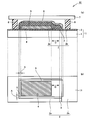
- (A) is a schematic sectional drawing which shows the layer structure of the wet solar cell of this invention
- (b) is the top view which looked at the wet solar cell of (a) from the non-light-receiving surface side.
- It is a schematic sectional drawing which shows the layer structure of the wet solar cell module of this invention. It is a graph which shows the relationship between the distance D and the film thickness Y of a porous insulating layer. It is a graph which shows the relationship between the distance A and the film thickness Y of a porous insulating layer.
- FIG. 1A is a schematic cross-sectional view showing the layer structure of the main part of the wet solar cell of the present invention (hereinafter also referred to as “solar cell” or “dye-sensitized solar cell”), and FIG. These are the figures which looked at the wet solar cell of Fig.1 (a) from the non-light-receiving surface side.
- the wet solar cell 10 of the present invention includes a support 1 and a laminate formed on the support 1 as shown in FIG.
- a conductive layer 2 In this laminate, a conductive layer 2, a photoelectric conversion layer 4, a porous insulating layer 5, and a counter electrode conductive layer 6 are laminated in this order.
- a cover layer 7 is provided above the counter electrode conductive layer 6, and a sealing material 8 is provided on both sides of the laminate.
- the conductive layer 2 is divided by a scribe line 3 into a first region 2a where the photoelectric conversion layer 4 is stacked and a second region 2b where the photoelectric conversion layer 4 is not stacked.
- the photoelectric conversion layer 4 is laminated on a part of the surface of the first region 2 a of the conductive layer 2. That is, the first region 2a includes a portion where the photoelectric conversion layer 4 is stacked and a portion where the photoelectric conversion layer 4 is not stacked.
- the distance D from the peripheral portion of the first region 2a facing the scribe line 3 to the peripheral portion of the photoelectric conversion layer 4 is 50 ⁇ m or more.
- the distance D is a distance between the average line of the boundary of the photoelectric conversion layer 4 facing the scribe line 3 side and the average line of the boundary of the scribe line 3 facing the photoelectric conversion layer 4 side of the first region 2a.
- the distance D is less than 50 ⁇ m, sagging, printing accuracy, and ink sneaking due to a decrease in printability occur during printing. As a result, a part of the porous semiconductor constituting the photoelectric conversion layer overlaps with the scribe line, and peeling occurs in processes such as drying and baking, which causes failure and yield reduction.
- the distance D is preferably 500 ⁇ m or less.
- Y is the film thickness ( ⁇ m) of the porous insulating layer
- D is the distance D ( ⁇ m), 50 ⁇ D ⁇ 500.
- the catalyst layer and the conductive layer existing on the light receiving surface side are short-circuited, and the location where physical leakage occurs is between the scribe line and the photoelectric conversion layer. The probability of doing is increased. Therefore, it is necessary to increase the thickness of the porous insulating layer as the area of this portion increases, and the relational expression is expressed by (1).
- the film thickness Y of the porous insulating layer satisfying the following formula (2) is secured.
- Y is the film thickness (micrometer) of a porous insulating layer
- D is the said distance D (micrometer).
- the film thickness Y of the porous insulating layer is a vertical distance from the surface of the conductive layer 2 to the outermost surface of the porous insulating layer 5, and in the portion where the photoelectric conversion layer of the first region 2a is not laminated. Refers to the thickness of the layer.
- the distance A from the outer edge of the counter electrode conductive layer projected on the light receiving surface not facing the scribe line 3 to the outer edge of the photoelectric conversion layer is 500 ⁇ m or less.
- the distance A specifically refers to the distance from the average line of the outer edge of the photoelectric conversion layer 4 on the side not facing the scribe line 3 side to the average line of the outer edge of the photoelectric conversion layer 4.
- the distance A is a distance from the outer edge of the counter electrode conductive layer projected onto the light receiving surface not facing the scribe line side to the outer edge of the photoelectric conversion layer not facing the scribe line side, and is 500 ⁇ m or less. It is characterized by that.
- the distance A is preferably 100 ⁇ m or less. If it exceeds 500 ⁇ m, the area of the portion where the counter electrode conductive layer (positive electrode) is not present on the photoelectric conversion layer (negative electrode) increases, and the moving distance of the electrolytic solution becomes long, which is not preferable. Since the moving distance by the Brownian motion of the electrolyte composition is several hundred ⁇ m, when the distance A exceeds 500 ⁇ m, the performance is remarkably deteriorated due to a voltage drop due to the movement of the electrolyte composition.
- the relationship between the counter electrode conductive layer and the conductive layer is satisfied by satisfying the relationship of the following formula (3). It is possible to suppress the leakage between the two.
- Y is the film thickness ( ⁇ m) of the porous insulating layer
- A is the distance A ( ⁇ m).
- the catalyst layer and the conductive layer existing on the light receiving surface side are short-circuited at the portion where the counter conductive layer protrudes from the photoelectric conversion layer, and physical leakage occurs. If the area of the protruding portion is large, the probability of leakage increases. Therefore, it is necessary to increase the thickness of the porous insulating layer as the area of this portion increases, and the relational expression is expressed by (3).
- the present invention is characterized in that when the distance A exceeds 500 ⁇ m, the thickness of the porous insulating layer is set to 16.5 ⁇ m or more.
- the film thickness Y of the porous insulating layer is a vertical distance from the surface of the conductive layer 2 to the outermost surface of the porous insulating layer 5, and the portion where the photoelectric conversion layer 4 of the first region 2a is not laminated. Refers to the thickness of the porous insulating layer.
- the support 1 needs to be light transmissive at the portion that becomes the light receiving surface of the solar cell, the support 1 is preferably made of at least a light transmissive material and has a thickness of about 0.2 to 5 mm.
- the material constituting the support 1 is not particularly limited as long as it is a material that can generally be used for solar cells and can exhibit the effects of the present invention.
- examples of such materials include glass substrates such as soda glass, fused silica glass, and crystal quartz glass, and heat resistant resin plates such as flexible films.
- film examples include tetraacetylcellulose (TAC), polyethylene terephthalate (PET), polyphenylene sulfide (PPS), polycarbonate (PC), and polyarylate. (PA), polyetherimide (PEI), phenoxy resin, polytetrafluoroethylene (PTFE), and the like.
- TAC tetraacetylcellulose
- PET polyethylene terephthalate
- PPS polyphenylene sulfide
- PC polycarbonate
- PA polyarylate
- PA polyetherimide
- PTFE polytetrafluoroethylene
- the flexible film When forming another layer with heating on the support 1, for example, when forming the conductive layer 2 with heating at about 250 ° C. on the support 1, the flexible film is formed.
- PTFE polytetrafluoroethylene
- the materials polytetrafluoroethylene (PTFE) having heat resistance of 250 ° C. or higher is particularly preferable.
- the support 1 can be used when the completed solar cell is attached to another structure. That is, the peripheral part of the support body 1 such as a glass substrate can be easily attached to another support body 1 using metal processed parts and screws.
- the conductive layer 2 is a light-receiving surface of the solar cell and needs to be light transmissive, and thus is made of a light transmissive material.
- any material may be used as long as it can substantially transmit light having a wavelength having an effective sensitivity to at least a sensitizing dye described later, and it is not always necessary to transmit light in all wavelength regions.
- the light-transmitting material for forming the conductive layer 2 is not particularly limited as long as it is a material that can be generally used for solar cells and can exhibit the effects of the present invention.
- examples of such materials include indium tin composite oxide (ITO), fluorine-doped tin oxide (FTO), and zinc oxide (ZnO).
- the structure in which the conductive layer 2 is laminated on the support 1 is sometimes referred to as a transparent electrode substrate 11.
- a transparent electrode substrate 11 include a transparent electrode substrate in which a conductive layer 2 made of FTO is laminated on a support 1 made of soda-lime float glass, and is preferably used in the present invention. .
- the film thickness of the conductive layer 2 is preferably about 0.02 to 5 ⁇ m, the film resistance is preferably as low as possible, and is preferably 40 ⁇ / sq or less.
- the conductive layer 2 may be provided with a metal lead wire for reducing the resistance.
- the metal lead wire material include platinum, gold, silver, copper, aluminum, nickel, and titanium.
- the thickness of the metal lead wire is preferably about 0.1 to 4 mm.
- the scribe line 3 is formed by cutting a conductive film constituting the conductive layer by laser scribe. Due to the scribe line 3, the conductive layer 2 includes a first region 2 a including a portion where a photoelectric conversion layer 4 described later is laminated and a portion where the photoelectric conversion layer 4 is not laminated, and the first where the photoelectric conversion layer 4 is not formed. It is divided into two regions 2b. The distance (the width of the scribe line) between the first region 2a and the second region 2b via the scribe line 3 is, for example, about 10 ⁇ m to 200 ⁇ m, depending on the size of the wet solar cell.
- the photoelectric conversion layer 4 is formed by adsorbing a dye or quantum dots to a layer made of a porous semiconductor and filling a carrier transport material.
- the porous semiconductor is composed of a semiconductor.
- the semiconductor can have various forms such as a bulk form, a particle form, and a film form having a large number of micropores, but a film-like form having a large number of micropores is preferable.
- the semiconductor material constituting the porous semiconductor is not particularly limited as long as it is generally used for a photoelectric conversion material.
- examples of such materials include titanium oxide, zinc oxide, tin oxide, iron oxide, niobium oxide, cerium oxide, tungsten oxide, nickel oxide, strontium titanate, cadmium sulfide, lead sulfide, zinc sulfide, indium phosphide, Examples include compounds such as copper-indium sulfide (CuInS 2 ), CuAlO 2 , SrCu 2 O 2 , and combinations thereof.
- titanium oxide, zinc oxide, tin oxide, and niobium oxide are preferable, and titanium oxide is particularly preferable from the viewpoint of photoelectric conversion efficiency, stability, and safety.
- these semiconductor materials can also be used as a mixture of two or more.
- the titanium oxide includes various narrowly defined titanium oxides such as anatase type titanium oxide, rutile type titanium oxide, amorphous titanium oxide, metatitanic acid, orthotitanic acid, titanium hydroxide, hydrous titanium oxide, and the like. These can be used alone or as a mixture.
- the two types of crystal systems, anatase type and rutile type can be in any form depending on the production method and thermal history, but the anatase type is common.
- the particle diameter of the fine particles is preferably 5 nm or more and less than 50 nm (preferably 10 nm or more and 30 nm or less) from the viewpoint of obtaining a sufficiently large effective surface area with respect to the projected area.
- incident light can be converted into electric energy with high yield.
- the average particle diameter in this specification is the value calculated
- required from the diffraction peak of XRD (X-ray diffraction). Specifically, the average particle diameter is determined from the half-value width of the diffraction angle in XRD ⁇ / 2 ⁇ measurement and Scherrer's equation. For example, in the case of anatase-type titanium oxide, the half-value width of the diffraction peak (2 ⁇ 25.3 ° vicinity) corresponding to the (101) plane may be measured.
- the light scattering property of the photoelectric conversion layer made of a porous semiconductor can be adjusted by the particle diameter (average particle diameter) of the semiconductor material used for layer formation.
- the photoelectric conversion layer made of a porous semiconductor Although it depends on the formation conditions of the photoelectric conversion layer made of a porous semiconductor, specifically, when a porous semiconductor formed of semiconductor particles having a large average particle diameter is included, the light scattering property is high, and incident light is scattered. The light capture rate can be improved.
- a porous semiconductor layer formed of semiconductor particles having a small average particle diameter has low light scattering properties, and can increase the adsorption amount by increasing the adsorption point of the dye.
- a layer made of semiconductor particles having an average particle diameter of preferably 50 nm or more, more preferably 50 nm to 600 nm may be provided on the polycrystalline sintered body made of the fine particles.
- the porous semiconductor which comprises the photoelectric converting layer in this invention may be a laminated structure.
- the average particle size of the porous semiconductor material is not particularly limited as long as it is within the above-described range in which the effects of the present invention can be exhibited. In terms of effective use of incident light for photoelectric conversion, it is more preferable that the average particle diameter is uniform to some extent as in a commercially available semiconductor material powder.
- an insulating layer is provided between a photoelectric conversion layer made of a porous semiconductor and a counter electrode.
- the particle size is large (in the present invention, 100 nm to A counter electrode conductive layer or a single conductive layer may be formed on a photoelectric conversion layer containing a porous semiconductor composed of fine particles.
- the photoelectric conversion layer containing a highly light-scattering porous semiconductor, particularly the photoelectric conversion layer in contact with the counter electrode conductive layer 6, has a low mechanical strength due to the large average particle size of the constituent semiconductor material, and the structure of the solar cell. Problems may occur.
- the photoelectric conversion layer may be mechanically strengthened by blending a semiconductor material having a small average particle size with a semiconductor material having a large average particle size, for example, at a ratio of 10% by weight or less of the whole material. Good.
- the film thickness of the photoelectric conversion layer is not particularly limited, but is preferably about 0.5 to 50 ⁇ m from the viewpoint of photoelectric conversion efficiency.
- the thickness of the layer is preferably 0.1 to 40 ⁇ m, more preferably 5 to 20 ⁇ m, and an average particle size of 5 nm or more.
- the thickness of the layer is preferably 0.1 to 50 ⁇ m, more preferably 10 to 40 ⁇ m.
- the membrane-like porous semiconductor preferably has a large specific surface area, and is preferably about 10 to 200 m 2 / g.
- the dye adsorbed on the porous semiconductor examples include organic dyes and metal complex dyes that absorb in various visible light regions and / or infrared light regions as long as they function as a photosensitizer. One or two or more of these dyes can be selectively used.
- organic dyes examples include azo dyes, quinone dyes, quinone imine dyes, quinacridone dyes, squarylium dyes, cyanine dyes, merocyanine dyes, triphenylmethane dyes, xanthene dyes, porphyrin dyes, and perylenes. And dyes such as indigo dyes, phthalocyanine dyes, and naphthalocyanine dyes.
- the extinction coefficient of organic dyes is generally larger than that of metal complex dyes in which molecules are coordinated to transition metals.
- metal complex dyes Cu, Ni, Fe, Co, V, Sn, Si, Ti, Ge, Cr, Zn, Ru, Mg, Al, Pb, Mn, In, Mo, Y, Zr, Nb, Sb, Metals such as La, W, Pt, Ta, Ir, Pd, Os, Ga, Tb, Eu, Rb, Bi, Se, As, Sc, Ag, Cd, Hf, Re, Au, Ac, Tc, Te, Rh Among them, phthalocyanine-based metal complex dyes and ruthenium-based metal complex dyes are preferable, and ruthenium-based metal complex dyes are particularly preferable.
- ruthenium-based metal complex dyes represented by the following chemical formulas (4) to (6) are preferable.
- the carboxylic acid group, carboxylic anhydride group, alkoxy group, hydroxyl group, hydroxyalkyl group, sulfonic acid group, ester group, mercapto group, phosphonyl group in the dye molecule Those having an interlocking group such as a group are preferred. Among these, a carboxylic acid group and a carboxylic anhydride group are particularly preferable.
- the interlock group provides an electrical bond that facilitates electron transfer between the excited dye and the conduction band of the porous semiconductor.
- Quantum dots that adsorb to a porous semiconductor and function as a photosensitizer include CdS, CdSe, PbS, PbSe, and the like.
- a porous insulating layer 5 is generally provided between the photoelectric conversion layer 4 and the counter electrode conductive layer 6.
- a material having a high conduction band level such as glass, zirconium oxide, silicon oxide, aluminum oxide, niobium oxide, strontium titanate, or the like is used.
- the porous insulating layer 5 include those composed of a particulate porous material. In this case, the average particle diameter is preferably 5 to 500 nm, and more preferably 10 to 300 nm.
- the counter electrode conductive layer 6 in the present invention includes a catalyst layer having a catalytic function and a function of reducing holes in the carrier transport layer, and a conductive layer having a function of collecting electrons and connecting in series with adjacent solar cells. These are collectively called a counter electrode conductive layer.
- a catalyst layer has high electroconductivity, or when a conductive layer has catalytic ability, it can be set as the counter electrode conductive layer 6 each independently.
- An embodiment in which a catalyst layer is further provided separately from the counter electrode conductive layer is also included in the present invention.
- the counter electrode conductive layer 6 is usually formed by forming the catalyst layer on the porous insulating layer 5 and then forming the conductive layer.
- the stacking order may be reversed from that of a normal wet solar cell, such as providing a conductive layer on the porous insulating layer 5 first and forming a catalyst layer on the conductive layer. This stacking order can prevent peeling of the counter electrode conductive layer from the catalyst layer.
- the material which comprises the conductive layer of the counter electrode conductive layer 6 will not be specifically limited if it is a material which can generally be used for a solar cell and can exhibit the effect of this invention.
- Such materials include indium tin composite oxide (ITO), metal oxides such as fluorine doped tin oxide (FTO), zinc oxide (ZnO), titanium, tungsten, gold, silver, copper, nickel, etc.
- ITO indium tin composite oxide
- metal oxides such as fluorine doped tin oxide (FTO), zinc oxide (ZnO), titanium, tungsten, gold, silver, copper, nickel, etc.
- a metal material is mentioned. Considering the film strength, titanium is most preferable.
- the film formation of the counter electrode conductive layer 6 by the vapor deposition method since the film itself is porous, it is not necessary to newly form holes through which the dye solution and the carrier transport material can move.
- the holes are about 1 nm to 20 nm.
- the catalyst layer 7 is formed on the counter electrode conductive layer 6, the catalyst layer material passes through the holes of the counter electrode conductive layer. It has been confirmed that it does not reach the porous insulating layer 5 and further the porous semiconductor layer (photoelectric conversion layer 7).
- the counter electrode conductive layer 6 When the catalyst layer 7 is formed from a platinum or carbon fine particle dispersion paste by a coating method, the counter electrode conductive layer 6 needs to be dense in order to suppress penetration of the fine particles. In this case, the formation of the holes in the counter electrode conductive layer 6 may be performed simultaneously with the catalyst layer 7 after the catalyst layer 7 is stacked.
- preferable counter electrode conductive layer materials are indium tin composite oxide (ITO), metal oxide such as fluorine-doped tin oxide (FTO), zinc oxide (ZnO), titanium, tungsten, gold, silver, copper, The material is not particularly limited as long as it is a material capable of forming a dense film such as a metal material such as nickel.
- the film thickness of the counter electrode conductive layer 6 is too thin, the resistance is high, and if it is too thick, it may be appropriately selected according to the specific resistivity of the material that hinders the movement of the carrier transport material.
- the hole is formed by, for example, partially evaporating by laser light irradiation.
- the holes have a diameter of 0.1 ⁇ m to 100 ⁇ m and an interval of 1 ⁇ m to 200 ⁇ m. Further, it is more preferable that the diameter of the hole is 1 ⁇ m to 100 ⁇ m and the interval is 5 ⁇ m to 200 ⁇ m.
- the material which comprises a catalyst layer will not be specifically limited if it is a material which can generally be used for a solar cell and can exhibit the effect of this invention.
- a material for example, platinum and carbon are preferable.
- As the form of carbon carbon black, graphite, glass carbon, amorphous carbon, hard carbon, soft carbon, carbon whisker, carbon nanotube, fullerene and the like are preferable.
- the cover layer 7 is important for preventing volatilization of the electrolytic solution and intrusion of water or the like into the battery.
- the material constituting the cover layer 7 is not particularly limited as long as it is a material that can generally be used for solar cells and can exhibit the effects of the present invention.
- examples of such materials include soda lime glass, lead glass, borosilicate glass, fused silica glass, and crystal quartz glass.
- a particularly preferred material is soda lime float glass.
- the sealing material 8 is important for preventing volatilization of the electrolytic solution and intrusion of water or the like into the battery.
- sealing material 8 is used for purposes such as (i) absorbing falling objects and stress (impact) acting on the support, (ii) absorbing deflection acting on the support during long-term use, and the like. Important to fulfill.
- the material constituting the sealing material 8 is not particularly limited as long as it is a material that can generally be used for solar cells and can exhibit the effects of the present invention.
- a silicone resin, an epoxy resin, a polyisobutylene resin, a polyamide resin, a hot melt resin such as a polyolefin resin and an ionomer resin, a glass frit, and the like are preferable. They can be used, or two or more can be used in a laminated structure of two or more layers.
- a nitrile solvent or a carbonate solvent is used as the solvent for the redox electrolyte
- a silicone resin, a hot melt resin, a polyisobutylene resin, and a glass frit are particularly preferable.
- the “carrier transport layer” is an area sandwiched between the conductive layer 2 and the cover layer 7 inside the sealing material 8 and supported by the sealing material 8. Refers to the implanted region. Therefore, at least the photoelectric conversion layer 4 and the porous insulating layer 5 are filled with the carrier transport material.
- the carrier transport material is composed of a conductive material capable of transporting ions, and examples of suitable materials include a liquid electrolyte, a solid electrolyte, a gel electrolyte, and a molten salt gel electrolyte.
- the liquid electrolyte is not particularly limited as long as it is a liquid substance containing a redox species and can generally be used in a battery or a solar battery. Specifically, those comprising a redox species and a solvent capable of dissolving this, those comprising a redox species and a molten salt capable of dissolving this, and those comprising a redox species, a solvent capable of dissolving this and a molten salt. Is mentioned.
- Examples of the redox species include I ⁇ / I 3 ⁇ series, Br 2 ⁇ / Br 3 ⁇ series, Fe 2 + / Fe 3+ series, and quinone / hydroquinone series.
- a combination of metal iodide such as lithium iodide (LiI), sodium iodide (NaI), potassium iodide (KI), calcium iodide (CaI 2 ) and iodine (I 2 ), tetraethylammonium ion Combinations of tetraalkylammonium salts and iodine such as dye (TEAI), tetrapropylammonium iodide (TPAI), tetrabutylammonium iodide (TBAI), tetrahexylammonium iodide (THAI), and lithium bromide (LiBr);
- a combination of a metal bromide such as sodium bromide (NaBr), potassium bromide (KBr), calcium bromide (CaBr 2 ) and bromine is preferable, and among these, a combination of LiI and I 2 is particularly preferable.
- examples of the solvent for the redox species include carbonate compounds such as propylene carbonate, nitrile compounds such as acetonitrile, alcohols such as ethanol, water, and aprotic polar substances. Among these, carbonate compounds and nitrile compounds are particularly preferable. Two or more of these solvents can be used in combination.
- the solid electrolyte may be any conductive material that can transport electrons, holes, and ions, and can be used as an electrolyte for a solar cell and has no fluidity.
- hole transport materials such as polycarbazole, electron transport materials such as tetranitrofluororenone, conductive polymers such as polyroll, polymer electrolytes obtained by solidifying liquid electrolytes with polymer compounds, copper iodide, thiocyanate
- Examples thereof include a p-type semiconductor such as copper acid, and an electrolyte obtained by solidifying a liquid electrolyte containing a molten salt with fine particles.
- the gel electrolyte is usually composed of an electrolyte and a gelling agent.
- gelling agents include polymer gelation such as crosslinked polyacrylic resin derivatives, crosslinked polyacrylonitrile derivatives, polyalkylene oxide derivatives, silicone resins, and polymers having a nitrogen-containing heterocyclic quaternary compound salt structure in the side chain. Agents and the like.
- the molten salt gel electrolyte is usually composed of the gel electrolyte as described above and a room temperature molten salt.
- the room temperature molten salt include nitrogen-containing heterocyclic quaternary ammonium salt compounds such as pyridinium salts and imidazolium salts.
- an additive to said electrolyte as needed.
- additives include nitrogen-containing aromatic compounds such as t-butylpyridine (TBP), dimethylpropylimidazole iodide (DMPII), methylpropylimidazole iodide (MPII), ethylmethylimidazole iodide (EMII),
- TBP t-butylpyridine
- DMPII dimethylpropylimidazole iodide
- MPII methylpropylimidazole iodide
- EMII ethylmethylimidazole iodide
- imidazole salts such as ethylimidazole iodide (EII) and hexylmethylimidazole iodide (HMII).
- the electrolyte concentration in the electrolyte is preferably in the range of 0.001 to 1.5 mol / liter, particularly preferably in the range of 0.01 to 0.7 mol / liter.
- incident light reaches the porous semiconductor layer on which the dye is adsorbed through the electrolytic solution, and the carriers are excited. For this reason, the performance may deteriorate depending on the electrolyte concentration used in the unit cell having the catalyst layer on the light receiving surface side. Therefore, it is preferable to set the electrolyte concentration in consideration of this point.
- the counter electrode conductive layer 6 is provided with an extraction electrode (not shown) as necessary. A current is taken out from the solar cell by the take-out electrode.
- the constituent material of the extraction electrode is not particularly limited as long as it is a material that can generally be used for solar cells and can exhibit the effects of the present invention.
- the method for producing a wet solar cell according to the present invention includes a conductive layer 2 on one surface of a support 1 made of a light transmissive material, a photoelectric conversion layer 4 in which a dye is adsorbed on a porous semiconductor, a porous insulating layer 5,
- the step of forming a laminated body in which the counter electrode conductive layer 6 is laminated in the order described above, the step of forming the sealing material 8 on the outer periphery of the laminated body, and the cover layer 7 supported by the sealing material 8 are arranged to face each other.
- the method for forming the transparent electrode substrate 11 by forming the conductive layer 2 on the support 1 is not particularly limited, and examples thereof include a known sputtering method and spray method.
- a metal lead wire (not shown) is provided on the conductive layer 2
- a metal lead wire is formed on the support 1 by a known sputtering method, vapor deposition method or the like, and then the support including the metal lead wire is formed.
- the conductive layer 2 may be formed on the substrate 1, or the metal lead may be formed on the conductive layer 2 after the conductive layer 2 is formed on the support 1.
- the scribe line 3 is formed by cutting the conductive layer 2 by laser scribe.
- a method of forming a layer made of a film-like porous semiconductor on the conductive layer 2 of the transparent electrode substrate 11 after applying a paste containing semiconductor particles on the conductive layer by a screen printing method, an inkjet method or the like, Examples thereof include a method of forming a film on a conductive layer by a firing method, a sol-gel method, a method using an electrochemical redox reaction, and the like.
- a screen printing method using a paste is particularly preferable because a layer made of a thick porous semiconductor can be formed at low cost.
- a layer made of a porous semiconductor is formed in the vicinity of the scribe line 3, but the distance D is preferably 50 ⁇ m or more.
- the relationship between the distance D between the peripheral edge of the conductive layer facing the scribe line and the peripheral edge of the photoelectric conversion layer is as described above.
- a method for forming a layer made of a porous semiconductor using titanium oxide as semiconductor particles will be specifically described.
- titanium isopropoxide manufactured by Kishida Chemical Co., Ltd.
- a sol liquid is prepared by heating this aqueous solution at 80 degreeC for 8 hours.
- the obtained sol solution is heated at 230 ° C. for 11 hours in a titanium autoclave to grow titanium oxide particles.
- the titanium oxide particles are dispersed with an ultrasonic wave for 30 minutes to prepare a colloidal solution containing titanium oxide particles having an average particle size (average primary particle size) of 15 nm.
- a 2-fold volume of ethanol is added to the obtained colloidal solution, and this is centrifuged at a rotational speed of 5000 rpm to obtain titanium oxide particles.
- the titanium oxide solid concentration is adjusted to 20 wt%, ethyl cellulose 10 wt%, and terpineol 64 wt%.
- Solvents used to prepare a paste containing semiconductor particles (suspended) include, besides the above, glyme solvents such as ethylene glycol monomethyl ether, alcohol solvents such as isopropyl alcohol, and mixtures such as isopropyl alcohol / toluene. A solvent, water, etc. are mentioned.
- a paste containing semiconductor particles is applied onto the conductive layer by the above method and baked to obtain a photoelectric conversion layer.
- conditions such as temperature, time, and atmosphere depending on the type of support and semiconductor particles used. Calcination can be performed, for example, in an air atmosphere or an inert gas atmosphere within a range of about 50 to 800 ° C. for about 10 seconds to 12 hours. This drying and baking can be performed once at a single temperature or twice or more at different temperatures.
- the method for forming the film-like porous insulating layer 5 on the layer made of a porous semiconductor is not particularly limited, and may be a known method. Specifically, a method of applying a paste containing semiconductor particles on the conductive layer by screen printing, an inkjet method, and the like, followed by baking, a sol-gel method, a method using an electrochemical redox reaction, etc. The method of forming into a film on a conductive layer is mentioned. Among these methods, a screen printing method using a paste is particularly preferable because a thick porous insulating layer can be formed at low cost.
- Examples of the method for forming the counter electrode conductive layer 6 on the porous insulating layer 5 include vapor deposition and printing. In film formation of the counter electrode conductive layer by the vapor deposition method, the film itself becomes porous, so that it is not necessary to newly form holes through which the dye solution and the carrier transport material can move.
- a method of partially evaporating by laser light irradiation can be used.
- Examples of the method for adsorbing the dye on the layer made of the porous semiconductor include a method of immersing the layer made of the porous semiconductor formed on the conductive layer 2 in a solution in which the dye is dissolved (dye adsorption solution).
- the solvent for dissolving the dye may be any solvent that dissolves the dye. Specifically, alcohols such as ethanol, ketones such as acetone, ethers such as diethyl ether and tetrahydrofuran, and nitrogen compounds such as acetonitrile.
- Halogenated aliphatic hydrocarbons such as chloroform, aliphatic hydrocarbons such as hexane, aromatic hydrocarbons such as benzene, esters such as ethyl acetate, water, and the like. Two or more of these solvents can be used in combination.
- the concentration of the dye in the solution can be appropriately adjusted depending on the kind of the dye and the solvent to be used, but is preferably as high as possible in order to improve the adsorption function, for example, 5 ⁇ 10 ⁇ 4 mol / liter. That is all you need.
- the sealing material 8 is produced by cutting out a heat-sealing film, an ultraviolet curable resin, or the like into a shape surrounding the laminate.
- the pattern of the sealing material 8 can be formed by a dispenser when silicone resin, epoxy resin, or glass frit is used. Moreover, when using hot melt resin, the pattern of the sealing material 8 can be formed by making the hole patterned in the sheet-like hot melt resin.
- the sealing material 8 is disposed between the transparent electrode substrate 11 and the cover layer 7 so as to be bonded together, and is fixed by heating or ultraviolet irradiation.
- the carrier transport material is injected from an electrolyte (carrier transport material) injection hole provided in advance in the cover layer and filled in the carrier transport layer.
- the electrolyte injection hole is sealed with an ultraviolet curable resin after the carrier transport material is injected.
- FIG. 2 is a schematic cross-sectional view showing the layer structure of the main part of the wet solar cell module of the present invention.
- the wet solar cell module 20 of the present invention is formed on a transparent electrode substrate 11 composed of a support 1 and a conductive layer 2 formed on one surface of the support 1 and on one surface of the transparent electrode substrate 11.
- the conductive layer 2, the photoelectric conversion layer 4, the porous insulating layer 5, the counter electrode conductive layer 6, and the optionally provided catalyst layer (not shown) in which a dye is adsorbed to a layer made of a porous semiconductor are stacked in the above order.
- the laminated body, the sealing material 8 formed on the outer periphery of the laminated body, the cover layer 7 which is disposed opposite to the catalyst layer by a certain distance and supported by the sealing material 8, and At least two or more solar cells including a wet solar cell sandwiched between the conductive layer 2 inside the sealing material 8 and the cover layer 7 and having a carrier transport layer carried by the sealing material 8 Are connected in series. That is, at least one of the two or more solar cells constituting the wet solar cell module may be the wet solar cell of the present invention.
- adjacent wet solar cells are electrically connected to a catalyst layer or a counter electrode conductive layer of one wet solar cell and a conductive layer of the other solar cell.
- the collecting electrode portion 13 may be formed on the conductive layer 2 outside the outermost sealing material 12 of the wet solar cell module 20.
- a transparent electrode substrate 11 (manufactured by Nippon Sheet Glass Co., Ltd., glass with SnO 2 film) having a size of 30 mm ⁇ 30 mm ⁇ thickness 1.0 mm was prepared.
- the transparent electrode substrate 11 is obtained by forming a conductive layer made of a SnO 2 film on a support made of glass.
- the scribe line 3 was formed by cutting the conductive layer of the transparent electrode substrate 11 by laser scribing.
- a paste containing zirconia particles (average particle size of 50 nm) was applied on the photoelectric conversion layer using a screen printer. Thereafter, the porous insulating layer 5 having various film thicknesses was formed by baking at 500 ° C. for 60 minutes.
- a catalyst layer was obtained by depositing Pt on the counter electrode conductive layer 6 at a deposition rate of 4 ⁇ / s using a mask on which a predetermined pattern was formed and a vapor deposition apparatus (model number: EVD500A, manufactured by Anelva Corporation). .
- the size and position of the catalyst layer were the same as those of the porous semiconductor layer.
- the above laminate was immersed in a dye adsorption solution prepared in advance at room temperature for 100 hours. Thereafter, the laminate was washed with ethanol and dried at about 60 ° C. for about 5 minutes to adsorb the dye to the photoelectric conversion layer.
- the dye solution for adsorption is a mixture of acetonitrile and t-butanol having a volume ratio of 1: 1 so that the dye of the above formula (4) (manufactured by Solaronix, trade name: Ruthenium 620 1H3TBA) has a concentration of 4 ⁇ 10 ⁇ 4 mol / liter. It was prepared by dissolving in a mixed solvent.
- the substrate on which the laminate was formed and the glass substrate were bonded together using a heat-sealing film (DuPont, High Milan 1855) cut out so as to surround the periphery of the laminate. And these were crimped
- the melted heat-sealing film serves as a sealing material.
- an electrolyte prepared in advance is injected from an electrolyte injection hole provided in advance on the glass substrate, and the electrolyte is injected using an ultraviolet curable resin (manufactured by ThreeBond, model number: 31X-101).
- the carrier transport material was filled in the carrier transport layer by sealing the holes.
- a wet solar cell (single cell) was completed as described above.
- the electrolyte was acetonitrile as a solvent, and LiI (Aldrich) was used as a redox species at a concentration of 0.1 mol / liter, and I 2 (Kishida Chemical Co.) was set at a concentration of 0.01 mol / liter. A thing was used. Furthermore, t-butylpyridine (manufactured by Aldrich) as an additive was prepared at a concentration of 0.5 mol / liter, and dimethylpropylimidazole iodide (manufactured by Shikoku Kasei Kogyo Co., Ltd.) was prepared at a concentration of 0.6 mol / liter.
- Ag paste product name: Dotite, manufactured by Fujikura Kasei Co., Ltd.
- Dotite manufactured by Fujikura Kasei Co., Ltd.
- Example 10 to 19 A wet solar cell by the same method as in Example 1 except that the distance A from the outer edge of the porous semiconductor layer (photoelectric conversion layer) on the side not facing the scribe line to the outer edge of the counter electrode conductive layer was changed. was made.
- the distance A from the outer edge of the porous semiconductor layer (photoelectric conversion layer) on the side not facing the scribe line to the outer edge of the counter electrode conductive layer is measured, and the outer edge of the counter electrode conductive layer is outside the outer edge of the photoelectric conversion layer.
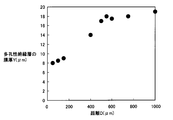
- FIG. 4 shows that the insulation film thickness Y increases almost linearly up to 500 ⁇ m with respect to the distance A, whereas the insulation film thickness is almost constant and does not change at 500 ⁇ m or more.
- Table 2 The relationship between Examples 10 to 19 and distance A is shown in Table 2 below.
- the film thickness of the porous insulating layer is required to be 20 ⁇ m or more, which causes a decrease in FF and tends to decrease the performance.
- the film thickness of the porous insulating layer is required to be 16.5 ⁇ m or more, which causes a decrease in FF and tends to decrease the performance.
- a transparent electrode substrate 11 manufactured by Nippon Sheet Glass Co., Ltd., trade name: glass with SnO 2 film: length 60 mm ⁇ width 37 mm
- the conductive layer 2 was cut by forming a scribe line 3 in parallel with the vertical direction of the SnO 2 film by laser scribing.
- the formed photoelectric conversion layer 4 has a thickness of 25 ⁇ m, a width of 5 mm, and a length of 50 mm, and is formed from the center of the porous semiconductor film, with one centered on the position 6.9 mm from the left end of the glass substrate. Three of the same size were formed at equal intervals.
- a porous insulating layer 5 was formed on the layer made of a porous semiconductor according to Example 1.
- the counter electrode conductive layer 6 was formed according to Example 1.
- the formed counter electrode conductive layer is formed to have a width of 5.6 mm and a length of 50 mm centered at a position of 7.2 mm from the left end of the transparent electrode substrate 11, and the center of the porous insulating layer 5 at the left end is formed. Three of the same size were formed at an interval of 7 mm to 7 mm.
- the counter electrode conductive layer 6 was formed according to Examples 16 to 19.
- the film thickness of the formed porous insulating layer was in accordance with the formula (3).
- Pt was formed on the counter electrode conductive layer 6 according to Example 1, and a catalyst layer was laminated.
- the size and position of the catalyst layer were the same as those of the layer 4 made of a porous semiconductor.
- the obtained laminate was immersed in the dye solution used in Example 1 at room temperature for 120 hours, and the dye was adsorbed on the layer made of the porous semiconductor to form the photoelectric conversion layer 4.
- an ultraviolet curable resin (31X-101, manufactured by ThreeBond Co., Ltd.) was applied between the laminates and around the cell using a dispenser (ULTRASAVE manufactured by EFD), and a glass substrate having a length of 60 mm and a width of 30 mm was bonded as a cover layer Then, the photosensitive resin was hardened by irradiating ultraviolet rays using an ultraviolet lamp (NOVACURE manufactured by EFD) to form the sealing material 8 and the outermost sealing material 12.
- a dispenser UTRASAVE manufactured by EFD
- Example 2 Thereafter, the same electrolytic solution as in Example 1 is injected from an electrolytic solution injection hole provided in advance on the glass substrate used as the cover layer 7, and further an ultraviolet curable resin is applied, and ultraviolet rays are irradiated in the same manner as the sealing material. Then, it was cured and sealed to form a carrier transport layer, and the module was completed.
- Ag paste (product name: Dotite, manufactured by Fujikura Kasei Co., Ltd.) was applied to the obtained module as a collector electrode part.
Abstract
Disclosed are: wet-type solar cells (10) wherein occurrence of malfunctions due to internal short-circuiting can be alleviated, and the yield thereof can be improved; and a wet-type solar cell module (20) using the wet-type solar cells (10). Each of the wet-type solar cells (10) is provided with a supporter (1) comprised of a light-transmissive material; and a laminate that has a conductive layer (2), a photoelectric conversion layer (4) comprised of a porous semiconductor containing no compact substance, a porous insulation layer (5), and an opposite-pole conductive layer (6) laminated on the supporter (1) in this order. The conductive layer (2) comprises a first area that has the photoelectric conversion layer (4) laminated thereupon, and a second area that does not have the photoelectric conversion layer (4) laminated thereupon, with a scribe line (3) interposed therebetween. The photoelectric conversion layer (4) is laminated on a portion of the surface of the first area, and the distance (D) from the circumferential-edge section of the first area facing the scribe line (3) to the circumferential-edge section of the photoelectric conversion layer (4) is made to be 50 μm or more.
Description
本発明は、湿式太陽電池および湿式太陽電池モジュールに関する。
The present invention relates to a wet solar cell and a wet solar cell module.
化石燃料に代るエネルギー源として、太陽光を電力に変換できる太陽電池が注目されている。現在、結晶系シリコン基板を用いた太陽電池および薄膜シリコン太陽電池が一部実用化され始めている。しかし、前者はシリコン基板の製造コストが高いという問題があり、後者は多種の半導体製造用ガスや複雑な装置を用いる必要があるために製造コストが高くなるという問題がある。このため、いずれの太陽電池においても光電変換の高効率化による発電出力当たりのコストを低減する努力が続けられているが、上記の問題を解決するには至っていない。
As an alternative energy source to fossil fuels, solar cells that can convert sunlight into electric power are attracting attention. At present, some solar cells and thin film silicon solar cells using a crystalline silicon substrate are beginning to be put into practical use. However, the former has a problem that the manufacturing cost of the silicon substrate is high, and the latter has a problem that the manufacturing cost becomes high because it is necessary to use various semiconductor manufacturing gases and complicated apparatuses. For this reason, although efforts have been made to reduce the cost per power generation output by increasing the efficiency of photoelectric conversion in any solar cell, the above problem has not been solved.
特開平01-220380号公報(特許文献1)には、新しいタイプの太陽電池として、金属錯体の光誘起電子移動を応用した湿式太陽電池が提案されている。この湿式太陽電池は、表面上に電極を形成した2枚のガラス基板の電極間に光電変換層を挟持したものである。光電変換層は、光増感色素を吸着させて可視光領域に吸収スペクトルをもたせた光電変換材料と電解質材料とからなる。
JP-A-01-220380 (Patent Document 1) proposes a wet solar cell applying photo-induced electron transfer of a metal complex as a new type of solar cell. In this wet solar cell, a photoelectric conversion layer is sandwiched between electrodes of two glass substrates on which electrodes are formed. The photoelectric conversion layer is composed of a photoelectric conversion material and an electrolyte material that have adsorbed a photosensitizing dye and have an absorption spectrum in the visible light region.
上記の湿式太陽電池に光が照射されると、光電変換層で電子が発生し、発生した電子が外部電気回路を通って電極に移動する。移動した電子が電解質中のイオンにより対向する電極に運ばれて光電変換層に戻る。このような一連の電子の流れにより、電気エネルギーが取り出される。
When the wet solar cell is irradiated with light, electrons are generated in the photoelectric conversion layer, and the generated electrons move to the electrode through an external electric circuit. The moved electrons are carried to the opposing electrode by ions in the electrolyte and return to the photoelectric conversion layer. Electrical energy is extracted by such a series of electron flows.
しかしながら、特許文献1に記載の色素増感太陽電池の基本構造は、対向する透明導電膜付きガラス基板間に電解液を注入した形態である。このため、小面積の太陽電池の試作は可能であっても、1m角のような大面積の太陽電池への適用は困難である。つまり、1つの太陽電池セルの面積を大きくすると、発生電流は面積に比例して増加するが、電極部分に用いる透明導電性膜の面内方向の電圧降下が増大し、太陽電池としての内部直列抵抗が増大する。その結果、光電変換時の電流電圧特性におけるFF(曲線因子)、および短絡電流が低下し、光電変換効率が低下するという問題が起こる。
However, the basic structure of the dye-sensitized solar cell described in Patent Document 1 is a form in which an electrolytic solution is injected between opposing glass substrates with a transparent conductive film. For this reason, even if trial manufacture of a solar cell with a small area is possible, application to a solar cell with a large area such as 1 m square is difficult. That is, when the area of one solar cell is increased, the generated current increases in proportion to the area, but the voltage drop in the in-plane direction of the transparent conductive film used for the electrode portion increases, and the internal series as a solar cell increases. Resistance increases. As a result, the FF (curve factor) and short circuit current in the current-voltage characteristics at the time of photoelectric conversion are lowered, resulting in a problem that photoelectric conversion efficiency is lowered.
国際公開第97/16838号パンフレット(特許文献2)には、1枚の透明導電膜付きガラス基板上に、複数の色素増感太陽電池を直列接続で配置した色素増感太陽電池モジュールが提案されている。この色素増感太陽電池モジュールは、1つの色素増感太陽電池の透明導電膜と、隣接する色素増感太陽電池の対極とを接触させることにより、両色素増感太陽電池を直列接続している。個々の色素増感太陽電池は、短冊形にパターニングされた透明導電膜(電極)を有する透明基板(ガラス基板)上に、光電変換層となる多孔性半導体層(多孔質酸化チタン層)、多孔性絶縁層(中間多孔性絶縁層)および対極(触媒層)を順次積層している。
International Publication No. 97/16838 (Patent Document 2) proposes a dye-sensitized solar cell module in which a plurality of dye-sensitized solar cells are arranged in series on a single glass substrate with a transparent conductive film. ing. This dye-sensitized solar cell module connects both dye-sensitized solar cells in series by bringing the transparent conductive film of one dye-sensitized solar cell into contact with the counter electrode of an adjacent dye-sensitized solar cell. . Each dye-sensitized solar cell has a porous semiconductor layer (porous titanium oxide layer) that becomes a photoelectric conversion layer on a transparent substrate (glass substrate) having a transparent conductive film (electrode) patterned in a strip shape, porous The conductive insulating layer (intermediate porous insulating layer) and the counter electrode (catalyst layer) are sequentially laminated.
特開2002-367686号公報(特許文献3)は、透明基板上に透明導電膜、緻密質からなる第1光電極、多孔質からなる第2光電極(多孔性半導体層)、セパレータおよび触媒(カーボン)層を有する集積化構造の色素増感太陽電池モジュールを開示している。この色素増感太陽電池モジュールは、緻密質からなる第1光電極を第2電極の直下に形成することにより、触媒層材料が透明導電膜に接触することを抑制している。さらに、触媒層材料の微粒子の平均粒径よりも小さい平均粒径を有する微粒子よりなる光電極層を設けることにより、触媒層微粒子が光電極層を通り抜け導電層に達することを防ぎ、内部短絡を防いでいる。
Japanese Patent Laid-Open No. 2002-367686 (Patent Document 3) discloses a transparent conductive film on a transparent substrate, a first photoelectrode made of dense material, a second photoelectrode made of porous material (porous semiconductor layer), a separator and a catalyst ( An integrated structure dye-sensitized solar cell module having a carbon) layer is disclosed. In this dye-sensitized solar cell module, the catalyst layer material is prevented from coming into contact with the transparent conductive film by forming the first photoelectrode made of a dense material directly below the second electrode. Furthermore, by providing a photoelectrode layer made of fine particles having an average particle size smaller than the average particle size of the fine particles of the catalyst layer material, it is possible to prevent the catalyst layer fine particles from passing through the photoelectrode layer and reaching the conductive layer, thereby preventing an internal short circuit. It is preventing.
特許文献3の色素増感太陽電池は、第1光電極および第2光電極(多孔性半導体層)が形成されている導電層を有する。カーボン層に接触する導電層部分がレーザースクライブ等により絶縁されている。第1電極および第2電極は、導電層の絶縁部端に合わせて形成されている。光電極をスクリーン印刷で形成する場合には、印刷の性質上、光電極等の印刷体の周囲に膜厚の薄い部分(ダレ)が生じる。このダレがサブミクロンオーダーの凹部となっている導電層の絶縁部に重なると、光電極等の印刷体に剥離が生じ、故障の発生、および歩留まりの低下をもたらす。
The dye-sensitized solar cell of Patent Document 3 has a conductive layer in which a first photoelectrode and a second photoelectrode (porous semiconductor layer) are formed. The conductive layer portion in contact with the carbon layer is insulated by laser scribing or the like. The first electrode and the second electrode are formed in accordance with the insulating portion end of the conductive layer. When the photoelectrode is formed by screen printing, a thin portion (sag) is generated around the printed body such as the photoelectrode due to the nature of printing. When this sagging overlaps with the insulating portion of the conductive layer which is a concave portion on the order of submicron, the printed material such as the photoelectrode is peeled off, resulting in a failure and a decrease in yield.
また、上記剥離を抑制するために、光電極の形成位置を絶縁部から離すと、その部分は対極導電層と導電層の間に多孔性絶縁層のみが存在する。発明者の検討の結果、対極導電層材料が導電層に接触することによる内部短絡の発生率は、対極導電層と導電層間に存在する層の膜厚に大きく依存することが判明した。よって、上記多孔性絶縁層だけが存在する導電層上では、内部短絡が頻発し、歩留まりの大幅な低下を引き起こすことがわかった。
Further, when the formation position of the photoelectrode is separated from the insulating portion in order to suppress the peeling, only the porous insulating layer exists between the counter electrode conductive layer and the conductive layer. As a result of the inventor's investigation, it has been found that the occurrence rate of internal short circuit due to the contact of the counter electrode conductive layer material with the conductive layer greatly depends on the thickness of the layer existing between the counter electrode conductive layer and the conductive layer. Therefore, it was found that internal short-circuits frequently occur on the conductive layer where only the porous insulating layer is present, causing a significant decrease in yield.
さらに、特許文献3に開示されているように、緻密層である第1光電極を形成すると、内部短絡が減少する一方で、最も光強度が強くなる部分の色素吸着量が低下し、発生電流が低下するという問題があった。
Furthermore, as disclosed in Patent Document 3, when the first photoelectrode that is a dense layer is formed, the internal short circuit is reduced, while the amount of dye adsorbed at the portion where the light intensity is strongest is reduced, and the generated current is reduced. There was a problem that decreased.
また、本発明者は、対極導電層と導電層との間の内部短絡の発生率を検討したところ、内部短絡の発生率は、対極導電層と導電層との間に存在する層の膜厚および面積に依存することが明らかとなった。すなわち、対極導電層と導電層との間に多孔性絶縁層のみが存在する場合は、内部短絡が頻発し、歩留まりが大幅に低下することが明らかとなった。
Further, the present inventor examined the occurrence rate of an internal short circuit between the counter electrode conductive layer and the conductive layer, and the occurrence rate of the internal short circuit is the film thickness of the layer existing between the counter electrode conductive layer and the conductive layer. And it became clear that it depends on the area. That is, when only the porous insulating layer is present between the counter electrode conductive layer and the conductive layer, it has been clarified that internal short-circuits frequently occur and the yield is greatly reduced.
このことから、受光面へ投影された対極導電層の外縁のうち、スクライブライン側に位置しないほうの外縁が、同様に受光面に投影された光電変換層の外縁よりも大きい場合、光電変換層からはみ出た対極導電層は、導電層との間に多孔性絶縁層のみが存在する。このため、多孔性絶縁層の厚みが薄いと、この部分における導電層上で内部短絡が頻発し、歩留まりの大幅な低下を引き起こすという問題があった。
Therefore, if the outer edge of the counter electrode conductive layer projected onto the light receiving surface is not located on the scribe line side, the outer edge of the photoelectric conversion layer similarly projected onto the light receiving surface is larger than the photoelectric conversion layer. Only the porous insulating layer exists between the protruding conductive layer and the conductive layer. For this reason, when the thickness of the porous insulating layer is thin, internal short-circuits frequently occur on the conductive layer in this portion, causing a problem that the yield is significantly reduced.
また、受光面に投影された対極導電層の外縁よりも、受光面に投影された光電変換層の外縁が大きい場合には、電極の発電部分上で対極がない部分が存在することになり、性能が著しく低下するという問題があった。
In addition, when the outer edge of the photoelectric conversion layer projected onto the light receiving surface is larger than the outer edge of the counter electrode conductive layer projected onto the light receiving surface, there will be a portion without the counter electrode on the power generation portion of the electrode, There was a problem that the performance was significantly reduced.
本発明は、上記課題に鑑みてなされたものであり、内部短絡による故障の発生を抑制し、歩留まりの向上を可能にした湿式太陽電池を提供すること、および該湿式太陽電池を用いた湿式太陽電池モジュールを提供することを目的とする。
The present invention has been made in view of the above problems, and provides a wet solar cell that suppresses the occurrence of a failure due to an internal short circuit and enables an improvement in yield, and a wet solar cell using the wet solar cell. An object is to provide a battery module.
本発明の湿式太陽電池は、光透過性の材料からなる支持体と、該支持体上に、導電層と、多孔性半導体からなる光電変換層と、多孔性絶縁層と、対極導電層とがこの順に積層された積層体を備えたものであって、導電層は、スクライブラインを介して、光電変換層が積層された第1の領域と、光電変換層が積層されていない第2の領域とを有し、光電変換層は、第1の領域の表面の一部に積層され、かつスクライブラインに面した第1の領域の周縁部から光電変換層の周縁部までの距離Dが50μm以上であることを特徴とする。上記の距離Dは500μm以下であることが好ましい。
The wet solar cell of the present invention comprises a support made of a light transmissive material, a conductive layer, a photoelectric conversion layer made of a porous semiconductor, a porous insulating layer, and a counter electrode conductive layer on the support. The conductive layer is provided with a stacked body that is stacked in this order, and the conductive layer includes, via a scribe line, a first region in which the photoelectric conversion layer is stacked and a second region in which the photoelectric conversion layer is not stacked. The photoelectric conversion layer is stacked on a part of the surface of the first region, and the distance D from the peripheral portion of the first region facing the scribe line to the peripheral portion of the photoelectric conversion layer is 50 μm or more It is characterized by being. The distance D is preferably 500 μm or less.
多孔性絶縁層の膜厚Yが以下の式(1)を満たすことが好ましい。
Y≧0.02D+6.5 …(1)
(式(1)中、Yは多孔性絶縁層の膜厚(μm)であり、Dは距離D(μm)である。)
距離Dが500μmを超え、多孔性絶縁層の膜厚Yが以下の式(2)を満たすことが好ましい。
Y≧16.5 …(2)
(式(2)中、Yは多孔性絶縁層の膜厚(μm)であり、Dは距離D(μm)である。)
本発明の湿式太陽電池は、光透過性の材料からなる支持体と、該支持体上に、導電層と、多孔性半導体からなる光電変換層と、多孔性絶縁層と、対極導電層とがこの順に積層された積層体を備えたものであって、導電層は、スクライブラインを介して、光電変換層が積層された第1の領域と、光電変換層が積層されていない第2の領域とを有し、該光電変換層は、第1の領域の表面の一部に積層され、かつ、スクライブラインに面していない側の受光面に投影された対極導電層の外縁から、光電変換層の外縁までの距離Aが、500μm以下であることを特徴とする。また、光電変換層の外縁が対極導電層の外縁よりも内側にある場合、距離Aと、多孔性絶縁層の膜厚Yとが以下の式(3)を満たすことが好ましい。
Y≧0.02A+6.5 …(3)
(式(3)中、Yは多孔性絶縁層の膜厚(μm)であり、Aは距離A(μm)である。)
本発明の湿式太陽電池は、光透過性の材料からなる支持体と、該支持体上に、導電層と、多孔性半導体からなる光電変換層と、多孔性絶縁層と、対極導電層とがこの順に積層された積層体を備えたものであって、該導電層は、スクライブラインを介して、光電変換層が積層された第1の領域と、光電変換層が積層されていない第2の領域とを有し、光電変換層は、第1の領域の表面の一部に積層され、かつ、スクライブラインに面していない側の受光面に投影された対極導電層の外縁から、光電変換層の外縁までの距離Aが、500μmを超え、該多孔性絶縁層の膜厚が16.5μm以上であることを特徴とする。 It is preferable that the film thickness Y of the porous insulating layer satisfies the following formula (1).
Y ≧ 0.02D + 6.5 (1)
(In Formula (1), Y is the film thickness (micrometer) of a porous insulating layer, and D is distance D (micrometer).)
It is preferable that the distance D exceeds 500 μm and the film thickness Y of the porous insulating layer satisfies the following formula (2).
Y ≧ 16.5 (2)
(In formula (2), Y is the film thickness (μm) of the porous insulating layer, and D is the distance D (μm).)
The wet solar cell of the present invention comprises a support made of a light transmissive material, a conductive layer, a photoelectric conversion layer made of a porous semiconductor, a porous insulating layer, and a counter electrode conductive layer on the support. The conductive layer is provided with a stacked body that is stacked in this order, and the conductive layer includes, via a scribe line, a first region in which the photoelectric conversion layer is stacked and a second region in which the photoelectric conversion layer is not stacked. The photoelectric conversion layer is laminated on a part of the surface of the first region and is photoelectrically converted from the outer edge of the counter electrode conductive layer projected onto the light receiving surface on the side not facing the scribe line. The distance A to the outer edge of the layer is 500 μm or less. Moreover, when the outer edge of a photoelectric converting layer exists inside the outer edge of a counter electrode conductive layer, it is preferable that the distance A and the film thickness Y of a porous insulating layer satisfy | fill the following formula | equation (3).
Y ≧ 0.02A + 6.5 (3)
(In formula (3), Y is the film thickness (μm) of the porous insulating layer, and A is the distance A (μm).)
The wet solar cell of the present invention comprises a support made of a light transmissive material, a conductive layer, a photoelectric conversion layer made of a porous semiconductor, a porous insulating layer, and a counter electrode conductive layer on the support. The conductive layer includes a stacked body stacked in this order, and the conductive layer includes a first region in which the photoelectric conversion layer is stacked and a second layer in which the photoelectric conversion layer is not stacked through a scribe line. The photoelectric conversion layer is laminated on a part of the surface of the first region, and photoelectric conversion is performed from the outer edge of the counter electrode conductive layer projected onto the light receiving surface on the side not facing the scribe line. The distance A to the outer edge of the layer exceeds 500 μm, and the film thickness of the porous insulating layer is 16.5 μm or more.
本発明によれば、2つ以上の湿式太陽電池が直列に接続された湿式太陽電池モジュールであって、上記いずれかの態様の湿式太陽電池を少なくとも1つ含み、上記直列接続は、隣接する湿式太陽電池の一方の湿式太陽電池の対極導電層と、他方の湿式太陽電池の導電層とが電気的に接続されることにより形成されている湿式太陽電池モジュールが提供される。
According to the present invention, there is provided a wet solar cell module in which two or more wet solar cells are connected in series, including at least one wet solar cell according to any one of the above aspects, wherein the series connection includes adjacent wet solar cells. There is provided a wet solar cell module formed by electrically connecting a counter electrode conductive layer of one wet solar cell of a solar cell and a conductive layer of the other wet solar cell.
本発明によれば、湿式太陽電池において上記で規定する距離Aが500μm以下であるか、または上記で規定する距離Dが50μm以上であることにより、内部短絡による故障の発生を抑制し、歩留まりの向上を可能にした湿式太陽電池を提供することができる。また、該湿式太陽電池を用いた湿式太陽電池モジュールを提供することができる。
According to the present invention, in the wet solar cell, when the distance A specified above is 500 μm or less, or the distance D specified above is 50 μm or more, the occurrence of a failure due to an internal short circuit is suppressed, and the yield is reduced. A wet solar cell that can be improved can be provided. Moreover, the wet solar cell module using this wet solar cell can be provided.
本発明の好適な実施形態について、図面を用いて説明する。なお、この実施形態は一例であり、種々の形態での実施が本発明の範囲内で可能である。本願の図面において同一の参照符号を付したものは、同一部分または相当部分を示している。
Preferred embodiments of the present invention will be described with reference to the drawings. In addition, this embodiment is an example and implementation with a various form is possible within the scope of the present invention. In the drawings of the present application, the same reference numerals denote the same or corresponding parts.
<湿式太陽電池>
図1(a)は、本発明の湿式太陽電池(以下、「太陽電池」または「色素増感太陽電池」ともいう)の要部の層構造を示す概略断面図であり、図1(b)は、図1(a)の湿式太陽電池を非受光面側から見た図である。 <Wet solar cell>
FIG. 1A is a schematic cross-sectional view showing the layer structure of the main part of the wet solar cell of the present invention (hereinafter also referred to as “solar cell” or “dye-sensitized solar cell”), and FIG. These are the figures which looked at the wet solar cell of Fig.1 (a) from the non-light-receiving surface side.
本発明の湿式太陽電池10は、図1(a)に示すように、支持体1と、支持体1上に形成された積層体とを備える。この積層体は、導電層2と、光電変換層4と、多孔性絶縁層5と、対極導電層6とがこの順に積層されたものである。対極導電層6の上方にはカバー層7が設けられ、積層体の両脇には封止材8が設けられる。
The wet solar cell 10 of the present invention includes a support 1 and a laminate formed on the support 1 as shown in FIG. In this laminate, a conductive layer 2, a photoelectric conversion layer 4, a porous insulating layer 5, and a counter electrode conductive layer 6 are laminated in this order. A cover layer 7 is provided above the counter electrode conductive layer 6, and a sealing material 8 is provided on both sides of the laminate.
本発明の湿式太陽電池において、導電層2はスクライブライン3により光電変換層4が積層される第1の領域2aと、光電変換層4が積層されない第2の領域2bとに分割される。上記光電変換層4は、上記導電層2の第1の領域2aの表面の一部に積層される。すなわち、上記第1の領域2aは、光電変換層4が積層される部分と光電変換層4が積層されない部分とを含む。本発明において、スクライブライン3に面した第1の領域2aの周縁部から光電変換層4の周縁部までの距離Dが50μm以上であることを特徴とする。
In the wet solar cell of the present invention, the conductive layer 2 is divided by a scribe line 3 into a first region 2a where the photoelectric conversion layer 4 is stacked and a second region 2b where the photoelectric conversion layer 4 is not stacked. The photoelectric conversion layer 4 is laminated on a part of the surface of the first region 2 a of the conductive layer 2. That is, the first region 2a includes a portion where the photoelectric conversion layer 4 is stacked and a portion where the photoelectric conversion layer 4 is not stacked. In the present invention, the distance D from the peripheral portion of the first region 2a facing the scribe line 3 to the peripheral portion of the photoelectric conversion layer 4 is 50 μm or more.
上記距離Dは、スクライブライン3側に面した光電変換層4の境界の平均線と、第1の領域2aの光電変換層4側に面したスクライブライン3の境界の平均線との間の距離をいう。
The distance D is a distance between the average line of the boundary of the photoelectric conversion layer 4 facing the scribe line 3 side and the average line of the boundary of the scribe line 3 facing the photoelectric conversion layer 4 side of the first region 2a. Say.
上記距離Dが50μm未満になると、印刷時に生じるダレや印刷精度、印刷性低下によるインクの回りこみなどが生じる。これにより光電変換層を構成する多孔性半導体の一部がスクライブラインと重なり、乾燥や焼成等の工程において剥離を生じ、故障、歩留まり低下の原因となる。
When the distance D is less than 50 μm, sagging, printing accuracy, and ink sneaking due to a decrease in printability occur during printing. As a result, a part of the porous semiconductor constituting the photoelectric conversion layer overlaps with the scribe line, and peeling occurs in processes such as drying and baking, which causes failure and yield reduction.
上記距離Dは500μm以下であることが好ましい。上記距離Dが500μm以下の場合は、導電層2と対極導電層6との短絡を抑制することができる。この場合、以下の式(1)の関係を満たすことが好ましい。
Y≧0.02D+6.5 …(1)
(式(1)中、Yは多孔性絶縁層の膜厚(μm)であり、Dは上記距離D(μm)、50≦D≦500である。)
発明者の検討によると、触媒層と受光面側に存在する導電層とが短絡し、物理的リークになる箇所は、スクライブラインと光電変換層の間であり、この部分の面積が大きいとリークする確率が高くなる。よって、この部分の面積の増大にしたがって、多孔性絶縁層の膜厚を大きくする必要があり、その関係式が(1)で表される。 The distance D is preferably 500 μm or less. When the distance D is 500 μm or less, a short circuit between theconductive layer 2 and the counter electrode conductive layer 6 can be suppressed. In this case, it is preferable to satisfy the relationship of the following formula (1).
Y ≧ 0.02D + 6.5 (1)
(In formula (1), Y is the film thickness (μm) of the porous insulating layer, and D is the distance D (μm), 50 ≦ D ≦ 500.)
According to the inventor's study, the catalyst layer and the conductive layer existing on the light receiving surface side are short-circuited, and the location where physical leakage occurs is between the scribe line and the photoelectric conversion layer. The probability of doing is increased. Therefore, it is necessary to increase the thickness of the porous insulating layer as the area of this portion increases, and the relational expression is expressed by (1).
Y≧0.02D+6.5 …(1)
(式(1)中、Yは多孔性絶縁層の膜厚(μm)であり、Dは上記距離D(μm)、50≦D≦500である。)
発明者の検討によると、触媒層と受光面側に存在する導電層とが短絡し、物理的リークになる箇所は、スクライブラインと光電変換層の間であり、この部分の面積が大きいとリークする確率が高くなる。よって、この部分の面積の増大にしたがって、多孔性絶縁層の膜厚を大きくする必要があり、その関係式が(1)で表される。 The distance D is preferably 500 μm or less. When the distance D is 500 μm or less, a short circuit between the
Y ≧ 0.02D + 6.5 (1)
(In formula (1), Y is the film thickness (μm) of the porous insulating layer, and D is the distance D (μm), 50 ≦ D ≦ 500.)
According to the inventor's study, the catalyst layer and the conductive layer existing on the light receiving surface side are short-circuited, and the location where physical leakage occurs is between the scribe line and the photoelectric conversion layer. The probability of doing is increased. Therefore, it is necessary to increase the thickness of the porous insulating layer as the area of this portion increases, and the relational expression is expressed by (1).
一方、Dが500μmを超える場合には、リークする確率が一定となり、下記の式(2)を満たす多孔性絶縁層の膜厚Yを確保すれば、リークを生じないことが判明した。
Y≧16.5 …(2)
(式(2)中、Yは多孔性絶縁層の膜厚(μm)、Dは上記距離D(μm)である。)
なお、多孔性絶縁層の膜厚Yは、導電層2表面から多孔性絶縁層5の最表面までの垂直距離であって、上記第1の領域2aの光電変換層が積層されていない部分における層の厚さをいう。 On the other hand, when D exceeds 500 μm, the probability of leakage is constant, and it has been found that leakage does not occur if the film thickness Y of the porous insulating layer satisfying the following formula (2) is secured.
Y ≧ 16.5 (2)
(In Formula (2), Y is the film thickness (micrometer) of a porous insulating layer, and D is the said distance D (micrometer).)
The film thickness Y of the porous insulating layer is a vertical distance from the surface of theconductive layer 2 to the outermost surface of the porous insulating layer 5, and in the portion where the photoelectric conversion layer of the first region 2a is not laminated. Refers to the thickness of the layer.
Y≧16.5 …(2)
(式(2)中、Yは多孔性絶縁層の膜厚(μm)、Dは上記距離D(μm)である。)
なお、多孔性絶縁層の膜厚Yは、導電層2表面から多孔性絶縁層5の最表面までの垂直距離であって、上記第1の領域2aの光電変換層が積層されていない部分における層の厚さをいう。 On the other hand, when D exceeds 500 μm, the probability of leakage is constant, and it has been found that leakage does not occur if the film thickness Y of the porous insulating layer satisfying the following formula (2) is secured.
Y ≧ 16.5 (2)
(In Formula (2), Y is the film thickness (micrometer) of a porous insulating layer, and D is the said distance D (micrometer).)
The film thickness Y of the porous insulating layer is a vertical distance from the surface of the
また、本発明は、図1(b)に示されるように、スクライブライン3に面していない側の受光面に投影された対極導電層の外縁から、光電変換層の外縁までの距離Aが、500μm以下であることを特徴とする。
Further, in the present invention, as shown in FIG. 1B, the distance A from the outer edge of the counter electrode conductive layer projected on the light receiving surface not facing the scribe line 3 to the outer edge of the photoelectric conversion layer is 500 μm or less.
上記距離Aは、具体的には、スクライブライン3側に面していない側の光電変換層4の外縁の平均線から、光電変換層4の外縁の平均線までの間の距離をいう。
The distance A specifically refers to the distance from the average line of the outer edge of the photoelectric conversion layer 4 on the side not facing the scribe line 3 side to the average line of the outer edge of the photoelectric conversion layer 4.
上記距離Aは、スクライブライン側に面していない側の受光面へ投影された対極導電層の外縁からスクライブライン側に面していない光電変換層の外縁までの距離であり、500μm以下であることを特徴とする。上記の距離Aは、100μm以下であることが好ましい。500μmを超えると、光電変換層上(負極)に対極導電層(正極)がない部分の面積が増大し、電解液の移動距離が長くなるため好ましくない。電解液組成物のブラウン運動による移動距離が数百μmであるため、距離Aが500μmを超える場合に電解液組成物の移動による電圧降下により性能が著しく低下する。
The distance A is a distance from the outer edge of the counter electrode conductive layer projected onto the light receiving surface not facing the scribe line side to the outer edge of the photoelectric conversion layer not facing the scribe line side, and is 500 μm or less. It is characterized by that. The distance A is preferably 100 μm or less. If it exceeds 500 μm, the area of the portion where the counter electrode conductive layer (positive electrode) is not present on the photoelectric conversion layer (negative electrode) increases, and the moving distance of the electrolytic solution becomes long, which is not preferable. Since the moving distance by the Brownian motion of the electrolyte composition is several hundred μm, when the distance A exceeds 500 μm, the performance is remarkably deteriorated due to a voltage drop due to the movement of the electrolyte composition.
光電変換層の外縁が対極導電層の外縁よりも内側にある場合、上記の距離Aが500μm以下の場合には、以下の式(3)の関係を満たすことにより対極導電層と導電層との間のリークを抑制することができる。
When the outer edge of the photoelectric conversion layer is inside the outer edge of the counter electrode conductive layer, when the distance A is 500 μm or less, the relationship between the counter electrode conductive layer and the conductive layer is satisfied by satisfying the relationship of the following formula (3). It is possible to suppress the leakage between the two.
Y≧0.02A+6.5 …(3)
(式(3)中、Yは多孔性絶縁層の膜厚(μm)であり、Aは上記距離A(μm)である。)
本発明者らの検討によると、対極導電層が光電変換層よりもはみ出した部分で、触媒層と受光面側に存在する導電層とが短絡し、物理的リークが起こる。このはみ出した部分の面積が大きいとリークする確率が高くなる。よって、この部分の面積の増大にしたがって、多孔性絶縁層の膜厚を大きくする必要があり、その関係式が(3)で表される。 Y ≧ 0.02A + 6.5 (3)
(In Formula (3), Y is the film thickness (μm) of the porous insulating layer, and A is the distance A (μm).)
According to the study by the present inventors, the catalyst layer and the conductive layer existing on the light receiving surface side are short-circuited at the portion where the counter conductive layer protrudes from the photoelectric conversion layer, and physical leakage occurs. If the area of the protruding portion is large, the probability of leakage increases. Therefore, it is necessary to increase the thickness of the porous insulating layer as the area of this portion increases, and the relational expression is expressed by (3).
一方、Aが500μmを超える場合には、リークする確率が一定となり、多孔性絶縁層の膜厚を16.5μm以上を確保すれば、リークを生じないことが判明した。すなわち、本発明は、距離Aが500μmを超えるときに、多孔性絶縁層の膜厚を16.5μm以上にすることを特徴とする。
On the other hand, when A exceeds 500 μm, the probability of leakage is constant, and it has been found that leakage does not occur if the thickness of the porous insulating layer is 16.5 μm or more. That is, the present invention is characterized in that when the distance A exceeds 500 μm, the thickness of the porous insulating layer is set to 16.5 μm or more.
なお、多孔性絶縁層の膜厚Yは、導電層2表面から多孔性絶縁層5の最表面までの垂直距離であって、上記第1の領域2aの光電変換層4が積層されていない部分における多孔性絶縁層の厚さをいう。本発明の湿式太陽電池の各構成について、以下詳細に説明する。
The film thickness Y of the porous insulating layer is a vertical distance from the surface of the conductive layer 2 to the outermost surface of the porous insulating layer 5, and the portion where the photoelectric conversion layer 4 of the first region 2a is not laminated. Refers to the thickness of the porous insulating layer. Each structure of the wet solar cell of this invention is demonstrated in detail below.
<支持体>
支持体1は、太陽電池の受光面となる部分では光透過性が必要となるため、少なくとも光透過性の材料からなり、厚さ0.2~5mm程度のものが好ましい。 <Support>
Since the support 1 needs to be light transmissive at the portion that becomes the light receiving surface of the solar cell, the support 1 is preferably made of at least a light transmissive material and has a thickness of about 0.2 to 5 mm.
支持体1を構成する材料は、一般に太陽電池に使用可能で、かつ本発明の効果を発揮し得る材料であれば、特に限定されない。このような材料としては、例えば、ソーダガラス、溶融石英ガラス、結晶石英ガラスなどのガラス基板、可撓性フィルムなどの耐熱性樹脂板などが挙げられる。
The material constituting the support 1 is not particularly limited as long as it is a material that can generally be used for solar cells and can exhibit the effects of the present invention. Examples of such materials include glass substrates such as soda glass, fused silica glass, and crystal quartz glass, and heat resistant resin plates such as flexible films.
上記可撓性フィルム(以下、「フィルム」ともいう)を構成する材料としては、例えば、テトラアセチルセルロース(TAC)、ポリエチレンテレフタレート(PET)、ポリフェニレンスルファイド(PPS)、ポリカーボネート(PC)、ポリアリレート(PA)、ポリエーテルイミド(PEI)、フェノキシ樹脂、ポリテトラフルオロエチレン(PTFE)などが挙げられる。
Examples of the material constituting the flexible film (hereinafter also referred to as “film”) include tetraacetylcellulose (TAC), polyethylene terephthalate (PET), polyphenylene sulfide (PPS), polycarbonate (PC), and polyarylate. (PA), polyetherimide (PEI), phenoxy resin, polytetrafluoroethylene (PTFE), and the like.
支持体1上に加熱を伴って他の層を形成する場合、例えば、支持体1上に250℃程度の加熱を伴って導電層2を形成する場合には、上記可撓性フィルムを構成する材料の中でも、250℃以上の耐熱性を有するポリテトラフルオロエチレン(PTFE)が特に好ましい。
When forming another layer with heating on the support 1, for example, when forming the conductive layer 2 with heating at about 250 ° C. on the support 1, the flexible film is formed. Among the materials, polytetrafluoroethylene (PTFE) having heat resistance of 250 ° C. or higher is particularly preferable.
また、完成した太陽電池を他の構造体に取り付けるときに支持体1を利用することができる。すなわち、ガラス基板などの支持体1の周辺部を、金属加工部品とねじを用いて他の支持体1に容易に取り付けることができる。
Also, the support 1 can be used when the completed solar cell is attached to another structure. That is, the peripheral part of the support body 1 such as a glass substrate can be easily attached to another support body 1 using metal processed parts and screws.
<導電層>
導電層2は、太陽電池の受光面となり、光透過性が必要となるため、光透過性の材料からなる。但し、少なくとも後述する増感色素に実効的な感度を有する波長の光を実質的に透過させる材料であればよく、必ずしもすべての波長領域の光に対して透過性を有する必要はない。 <Conductive layer>
Theconductive layer 2 is a light-receiving surface of the solar cell and needs to be light transmissive, and thus is made of a light transmissive material. However, any material may be used as long as it can substantially transmit light having a wavelength having an effective sensitivity to at least a sensitizing dye described later, and it is not always necessary to transmit light in all wavelength regions.
導電層2は、太陽電池の受光面となり、光透過性が必要となるため、光透過性の材料からなる。但し、少なくとも後述する増感色素に実効的な感度を有する波長の光を実質的に透過させる材料であればよく、必ずしもすべての波長領域の光に対して透過性を有する必要はない。 <Conductive layer>
The
導電層2を形成する光透過性の材料は、一般に太陽電池に使用可能で、かつ本発明の効果を発揮し得る材料であれば、特に限定されない。このような材料としては、インジウム錫複合酸化物(ITO)、フッ素をドープした酸化錫(FTO)、酸化亜鉛(ZnO)などが挙げられる。
The light-transmitting material for forming the conductive layer 2 is not particularly limited as long as it is a material that can be generally used for solar cells and can exhibit the effects of the present invention. Examples of such materials include indium tin composite oxide (ITO), fluorine-doped tin oxide (FTO), and zinc oxide (ZnO).
本発明において、上記支持体1に導電層2が積層された構造体を透明電極基板11ということがある。このような透明電極基板11としては、具体的には、ソーダ石灰フロートガラスからなる支持体1上に、FTOからなる導電層2を積層した透明電極基板が挙げられ、本発明において好適に用いられる。
In the present invention, the structure in which the conductive layer 2 is laminated on the support 1 is sometimes referred to as a transparent electrode substrate 11. Specific examples of such a transparent electrode substrate 11 include a transparent electrode substrate in which a conductive layer 2 made of FTO is laminated on a support 1 made of soda-lime float glass, and is preferably used in the present invention. .
上記導電層2の膜厚は0.02~5μm程度が好ましく、膜抵抗は低いほどよく、40Ω/sq以下が好ましい。
The film thickness of the conductive layer 2 is preferably about 0.02 to 5 μm, the film resistance is preferably as low as possible, and is preferably 40Ω / sq or less.
また、導電層2には、低抵抗化のために金属リード線を設けてもよい。金属リード線の材料としては、例えば、白金、金、銀、銅、アルミニウム、ニッケル、チタンなどが挙げられる。但し、金属リード線を設けることにより、受光面からの入射光量の低下を招く場合には、金属リード線の太さを0.1~4mm程度にするのが好ましい。
Further, the conductive layer 2 may be provided with a metal lead wire for reducing the resistance. Examples of the metal lead wire material include platinum, gold, silver, copper, aluminum, nickel, and titanium. However, when the metal lead wire is provided to reduce the amount of incident light from the light receiving surface, the thickness of the metal lead wire is preferably about 0.1 to 4 mm.
<スクライブライン>
スクライブライン3は、導電層を構成する導電膜をレーザースクライブにより切断して形成する。スクライブライン3により、導電層2は、後述の光電変換層4が積層された部分と光電変換層4が積層されていない部分とを含む第1の領域2aと、光電変換層4が形成されない第2の領域2bとに分割される。スクライブライン3を介した第1の領域2aと第2の領域2bとの距離(スクライブラインの幅)は、湿式太陽電池のサイズなどによるが、例えば10μm~200μm程度である。 <Scribe line>
Thescribe line 3 is formed by cutting a conductive film constituting the conductive layer by laser scribe. Due to the scribe line 3, the conductive layer 2 includes a first region 2 a including a portion where a photoelectric conversion layer 4 described later is laminated and a portion where the photoelectric conversion layer 4 is not laminated, and the first where the photoelectric conversion layer 4 is not formed. It is divided into two regions 2b. The distance (the width of the scribe line) between the first region 2a and the second region 2b via the scribe line 3 is, for example, about 10 μm to 200 μm, depending on the size of the wet solar cell.
スクライブライン3は、導電層を構成する導電膜をレーザースクライブにより切断して形成する。スクライブライン3により、導電層2は、後述の光電変換層4が積層された部分と光電変換層4が積層されていない部分とを含む第1の領域2aと、光電変換層4が形成されない第2の領域2bとに分割される。スクライブライン3を介した第1の領域2aと第2の領域2bとの距離(スクライブラインの幅)は、湿式太陽電池のサイズなどによるが、例えば10μm~200μm程度である。 <Scribe line>
The
<光電変換層>
光電変換層4は、多孔性半導体からなる層に色素や量子ドットを吸着させかつキャリア輸送材料を充填させてなる。 <Photoelectric conversion layer>
Thephotoelectric conversion layer 4 is formed by adsorbing a dye or quantum dots to a layer made of a porous semiconductor and filling a carrier transport material.
光電変換層4は、多孔性半導体からなる層に色素や量子ドットを吸着させかつキャリア輸送材料を充填させてなる。 <Photoelectric conversion layer>
The
<多孔性半導体>
上記多孔性半導体は、半導体から構成される。半導体の形態は、バルク状、粒子状、多数の微細孔を有する膜状など、種々の形態のものを用いることができるが、多数の微細孔を有する膜状の形態が好ましい。 <Porous semiconductor>
The porous semiconductor is composed of a semiconductor. The semiconductor can have various forms such as a bulk form, a particle form, and a film form having a large number of micropores, but a film-like form having a large number of micropores is preferable.
多孔性半導体を構成する半導体材料としては、一般に光電変換材料に使用されるものであれば特に限定されない。このような材料としては、例えば、酸化チタン、酸化亜鉛、酸化錫、酸化鉄、酸化ニオブ、酸化セリウム、酸化タングステン、酸化ニッケル、チタン酸ストロンチウム、硫化カドミウム、硫化鉛、硫化亜鉛、リン化インジウム、銅-インジウム硫化物(CuInS2)、CuAlO2、SrCu2O2などの化合物およびこれらの組み合せが挙げられる。これらの中でも、酸化チタン、酸化亜鉛、酸化錫、酸化ニオブが好ましく、光電変換効率、安定性および安全性の点から酸化チタンが特に好ましい。また、これらの半導体材料は、2種以上の混合物として用いることもできる。
The semiconductor material constituting the porous semiconductor is not particularly limited as long as it is generally used for a photoelectric conversion material. Examples of such materials include titanium oxide, zinc oxide, tin oxide, iron oxide, niobium oxide, cerium oxide, tungsten oxide, nickel oxide, strontium titanate, cadmium sulfide, lead sulfide, zinc sulfide, indium phosphide, Examples include compounds such as copper-indium sulfide (CuInS 2 ), CuAlO 2 , SrCu 2 O 2 , and combinations thereof. Among these, titanium oxide, zinc oxide, tin oxide, and niobium oxide are preferable, and titanium oxide is particularly preferable from the viewpoint of photoelectric conversion efficiency, stability, and safety. Moreover, these semiconductor materials can also be used as a mixture of two or more.
本発明において、酸化チタンは、アナターゼ型酸化チタン、ルチル型酸化チタン、無定形酸化チタン、メタチタン酸、オルソチタン酸などの各種の狭義の酸化チタンおよび水酸化チタン、含水酸化チタンなどを包含し、これらは単独または混合物として用いることができる。アナターゼ型とルチル型の2種類の結晶系は、その製法や熱履歴によりいずれの形態にもなり得るが、アナターゼ型が一般的である。
In the present invention, the titanium oxide includes various narrowly defined titanium oxides such as anatase type titanium oxide, rutile type titanium oxide, amorphous titanium oxide, metatitanic acid, orthotitanic acid, titanium hydroxide, hydrous titanium oxide, and the like. These can be used alone or as a mixture. The two types of crystal systems, anatase type and rutile type, can be in any form depending on the production method and thermal history, but the anatase type is common.
上記微粒子の粒径は、投影面積に対して十分に大きい実効表面積を得る観点から、平均粒径5nm以上50nm未満(好ましくは10nm以上30nm以下)が好ましい。このような微粒子を用いることにより入射光を高い収率で電気エネルギーに変換することができる。
The particle diameter of the fine particles is preferably 5 nm or more and less than 50 nm (preferably 10 nm or more and 30 nm or less) from the viewpoint of obtaining a sufficiently large effective surface area with respect to the projected area. By using such fine particles, incident light can be converted into electric energy with high yield.
なお、本明細書における平均粒径は、XRD(X線回折)の回折ピークから求めた値である。具体的には、XRDのθ/2θ測定における回折角の半値幅とシェラーの式から平均粒径を求める。例えば、アナターゼ型酸化チタンの場合、(101)面に対応する回折ピーク(2θ=25.3°付近)の半値幅を測定すればよい。
In addition, the average particle diameter in this specification is the value calculated | required from the diffraction peak of XRD (X-ray diffraction). Specifically, the average particle diameter is determined from the half-value width of the diffraction angle in XRD θ / 2θ measurement and Scherrer's equation. For example, in the case of anatase-type titanium oxide, the half-value width of the diffraction peak (2θ = 25.3 ° vicinity) corresponding to the (101) plane may be measured.
多孔性半導体からなる光電変換層の光散乱性は、層形成に用いる半導体材料の粒子径(平均粒径)により調整することができる。
The light scattering property of the photoelectric conversion layer made of a porous semiconductor can be adjusted by the particle diameter (average particle diameter) of the semiconductor material used for layer formation.
多孔性半導体からなる光電変換層の形成条件にもよるが、具体的には、平均粒径の大きい半導体粒子で形成した多孔性半導体を含む場合は、光散乱性が高く、入射光を散乱させ光捕捉率を向上させることができる。また、平均粒径の小さい半導体粒子で形成した多孔性半導体層は、光散乱性が低く、色素の吸着点をより多くし吸着量を増加させることができる。
Although it depends on the formation conditions of the photoelectric conversion layer made of a porous semiconductor, specifically, when a porous semiconductor formed of semiconductor particles having a large average particle diameter is included, the light scattering property is high, and incident light is scattered. The light capture rate can be improved. In addition, a porous semiconductor layer formed of semiconductor particles having a small average particle diameter has low light scattering properties, and can increase the adsorption amount by increasing the adsorption point of the dye.
したがって本発明において、上記微粒子からなる多結晶焼結体の上に、好ましくは平均粒径が50nm以上、より好ましくは平均粒径が50nm以上600nm以下の半導体粒子からなる層を設けてもよい。このように本発明における光電変換層を構成する多孔性半導体は積層構造であってもよい。
Therefore, in the present invention, a layer made of semiconductor particles having an average particle diameter of preferably 50 nm or more, more preferably 50 nm to 600 nm may be provided on the polycrystalline sintered body made of the fine particles. Thus, the porous semiconductor which comprises the photoelectric converting layer in this invention may be a laminated structure.
多孔性半導体材料の平均粒径は、本発明の効果を発揮し得る上記の範囲内であれば好ましく、特に限定されない。入射光を光電変換に有効利用するという点では、市販の半導体材料粉末のようにある程度平均粒径が揃っていることがより好ましい。
The average particle size of the porous semiconductor material is not particularly limited as long as it is within the above-described range in which the effects of the present invention can be exhibited. In terms of effective use of incident light for photoelectric conversion, it is more preferable that the average particle diameter is uniform to some extent as in a commercially available semiconductor material powder.
多孔性半導体からなる光電変換層と対極との間に絶縁層を設けるのが一般的であるが、特開2007-194039号公報で開示されるように粒径の大きい(本発明においては100nm~500nm程度)微粒子からなる多孔性半導体を含む光電変換層上に対極導電層、あるいは導電層単層を形成しても良い。光散乱性の高い多孔性半導体を含む光電変換層、特に対極導電層6と接触する光電変換層は、構成する半導体材料の平均粒径が大きいために機械的強度が低く、太陽電池の構造としての問題が起こることもある。このような場合には、平均粒径の大きい半導体材料に平均粒径の小さい半導体材料を、例えば材料全体の10重量%以下の割合で配合して、光電変換層を機械的に強化してもよい。
In general, an insulating layer is provided between a photoelectric conversion layer made of a porous semiconductor and a counter electrode. However, as disclosed in Japanese Patent Application Laid-Open No. 2007-194039, the particle size is large (in the present invention, 100 nm to A counter electrode conductive layer or a single conductive layer may be formed on a photoelectric conversion layer containing a porous semiconductor composed of fine particles. The photoelectric conversion layer containing a highly light-scattering porous semiconductor, particularly the photoelectric conversion layer in contact with the counter electrode conductive layer 6, has a low mechanical strength due to the large average particle size of the constituent semiconductor material, and the structure of the solar cell. Problems may occur. In such a case, the photoelectric conversion layer may be mechanically strengthened by blending a semiconductor material having a small average particle size with a semiconductor material having a large average particle size, for example, at a ratio of 10% by weight or less of the whole material. Good.
光電変換層(多孔性半導体層)の膜厚は、特に限定されるものではないが、光電変換効率の観点から、0.5~50μm程度が好ましい。特に、光散乱性の高い、平均粒径50nm以上の半導体粒子からなる層を設ける場合、その層の膜厚は、好ましくは0.1~40μm、より好ましくは5~20μm、平均粒径5nm以上50nm未満の半導体粒子よりなる層を設ける場合、その層の膜厚は、好ましくは0.1~50μm、より好ましくは10~40μmである。
The film thickness of the photoelectric conversion layer (porous semiconductor layer) is not particularly limited, but is preferably about 0.5 to 50 μm from the viewpoint of photoelectric conversion efficiency. In particular, when a layer made of semiconductor particles having a high light scattering property and an average particle size of 50 nm or more is provided, the thickness of the layer is preferably 0.1 to 40 μm, more preferably 5 to 20 μm, and an average particle size of 5 nm or more. When a layer made of semiconductor particles less than 50 nm is provided, the thickness of the layer is preferably 0.1 to 50 μm, more preferably 10 to 40 μm.
湿式太陽電池の光電変換効率を向上させるためには、後述する色素を多孔性半導体により多く吸着させて、光電変換層を形成することが必要である。このため、膜状の多孔性半導体は、比表面積の大きなものが好ましく、10~200m2/g程度が好ましい。
In order to improve the photoelectric conversion efficiency of the wet solar cell, it is necessary to form a photoelectric conversion layer by adsorbing more dyes described later to the porous semiconductor. For this reason, the membrane-like porous semiconductor preferably has a large specific surface area, and is preferably about 10 to 200 m 2 / g.
<光増感剤>
多孔性半導体に吸着させる色素としては、光増感剤として機能するものであれば、種々の可視光領域および/または赤外光領域に吸収をもつ有機色素、金属錯体色素などが挙げることができ、これらの色素を1種または2種以上を選択的に用いることができる。 <Photosensitizer>
Examples of the dye adsorbed on the porous semiconductor include organic dyes and metal complex dyes that absorb in various visible light regions and / or infrared light regions as long as they function as a photosensitizer. One or two or more of these dyes can be selectively used.
有機色素としては、例えば、アゾ系色素、キノン系色素、キノンイミン系色素、キナクリドン系色素、スクアリリウム系色素、シアニン系色素、メロシアニン系色素、トリフェニルメタン系色素、キサンテン系色素、ポルフィリン系色素、ペリレン系色素、インジゴ系色素、フタロシアニン系色素、ナフタロシアニン系色素などが挙げられる。
Examples of organic dyes include azo dyes, quinone dyes, quinone imine dyes, quinacridone dyes, squarylium dyes, cyanine dyes, merocyanine dyes, triphenylmethane dyes, xanthene dyes, porphyrin dyes, and perylenes. And dyes such as indigo dyes, phthalocyanine dyes, and naphthalocyanine dyes.
有機色素の吸光係数は、一般的に、遷移金属に分子が配位結合した形態をとる金属錯体色素に比べて大きい。
The extinction coefficient of organic dyes is generally larger than that of metal complex dyes in which molecules are coordinated to transition metals.
金属錯体色素としては、Cu、Ni、Fe、Co、V、Sn、Si、Ti、Ge、Cr、Zn、Ru、Mg、Al、Pb、Mn、In、Mo、Y、Zr、Nb、Sb、La、W、Pt、Ta、Ir、Pd、Os、Ga、Tb、Eu、Rb、Bi、Se、As、Sc、Ag、Cd、Hf、Re、Au、Ac、Tc、Te、Rhなどの金属に分子が配位結合した形態のものが挙げられ、これらの中でも、フタロシアニン系金属錯体色素、ルテニウム系金属錯体色素が好ましく、ルテニウム系金属錯体色素が特に好ましい。
As metal complex dyes, Cu, Ni, Fe, Co, V, Sn, Si, Ti, Ge, Cr, Zn, Ru, Mg, Al, Pb, Mn, In, Mo, Y, Zr, Nb, Sb, Metals such as La, W, Pt, Ta, Ir, Pd, Os, Ga, Tb, Eu, Rb, Bi, Se, As, Sc, Ag, Cd, Hf, Re, Au, Ac, Tc, Te, Rh Among them, phthalocyanine-based metal complex dyes and ruthenium-based metal complex dyes are preferable, and ruthenium-based metal complex dyes are particularly preferable.
特に、下記化学式(4)~(6)で表されるルテニウム系金属錯体色素が好ましい。
In particular, ruthenium-based metal complex dyes represented by the following chemical formulas (4) to (6) are preferable.
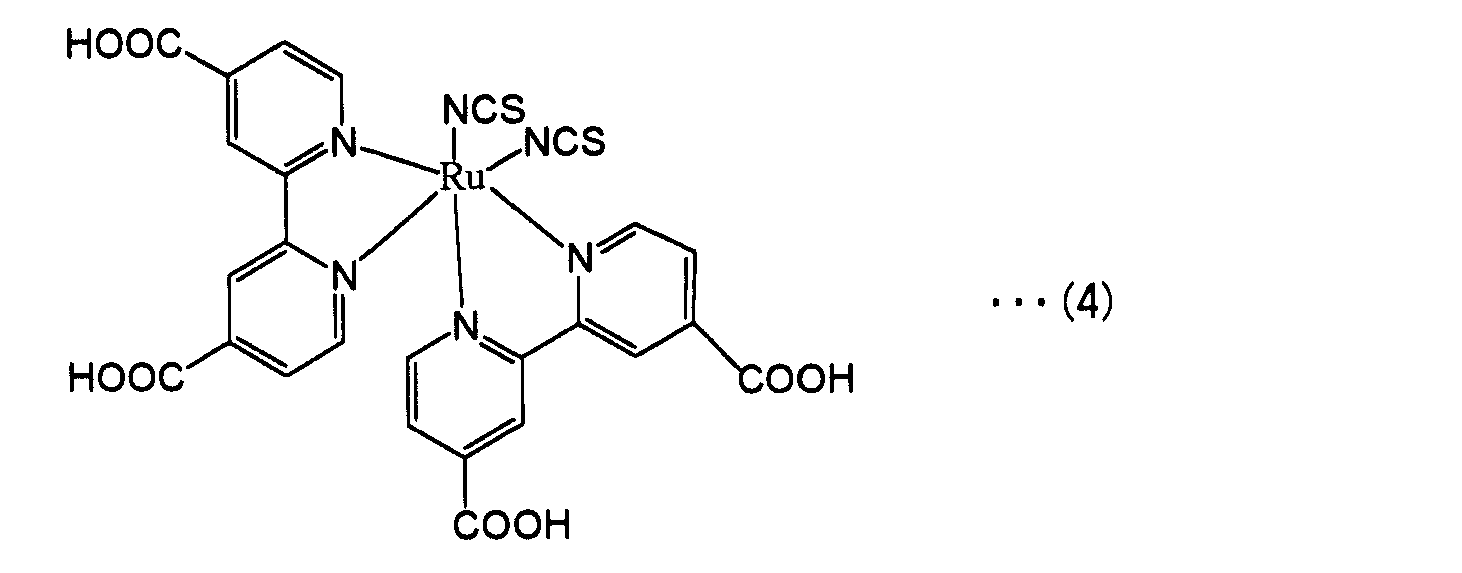
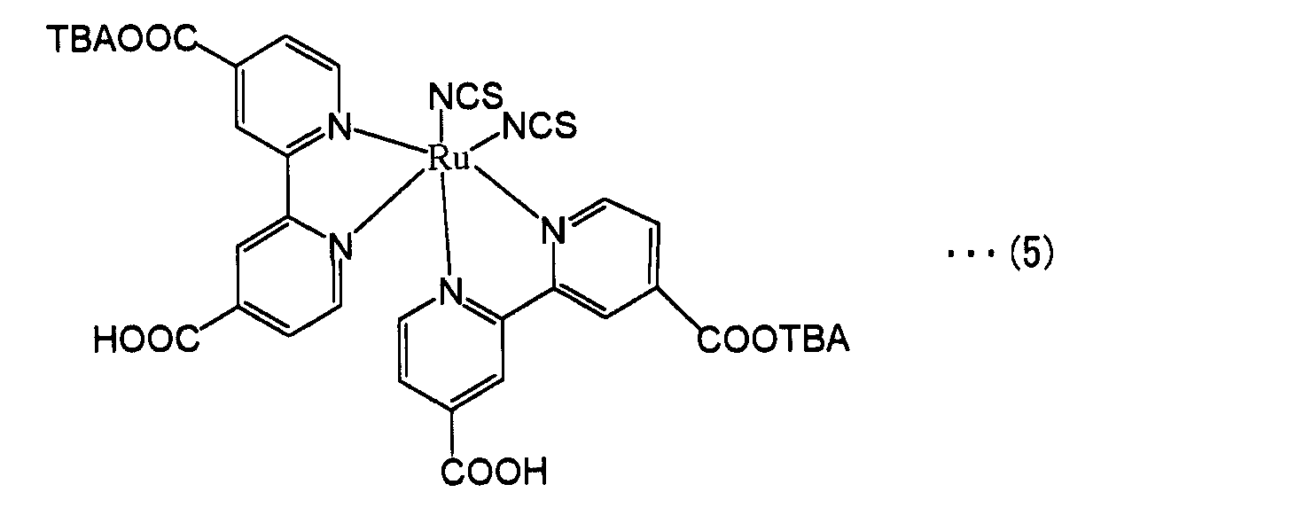

また、多孔性半導体に色素を強固に吸着させるためには、色素分子中にカルボン酸基、カルボン酸無水基、アルコキシ基、ヒドロキシル基、ヒドロキシアルキル基、スルホン酸基、エステル基、メルカプト基、ホスホニル基などのインターロック基を有するものが好ましい。これらの中でも、カルボン酸基およびカルボン酸無水基が特に好ましい。なお、インターロック基は、励起状態の色素と多孔性半導体の伝導帯との間の電子移動を容易にする電気的結合を提供するものである。
In order to strongly adsorb the dye to the porous semiconductor, the carboxylic acid group, carboxylic anhydride group, alkoxy group, hydroxyl group, hydroxyalkyl group, sulfonic acid group, ester group, mercapto group, phosphonyl group in the dye molecule Those having an interlocking group such as a group are preferred. Among these, a carboxylic acid group and a carboxylic anhydride group are particularly preferable. The interlock group provides an electrical bond that facilitates electron transfer between the excited dye and the conduction band of the porous semiconductor.
多孔性半導体に吸着して光増感剤として機能する量子ドットとしては、CdS,CdSe,PbS,PbSeなどが挙げられる。
Quantum dots that adsorb to a porous semiconductor and function as a photosensitizer include CdS, CdSe, PbS, PbSe, and the like.
<多孔性絶縁層>
湿式太陽電池において、光電変換層4と対極導電層6との間に多孔性絶縁層5を設けるのが一般的である。多孔性絶縁層5の材料としてはガラスや、酸化ジルコニウム、酸化ケイ素、酸化アルミニウム、酸化ニオブ、チタン酸ストロンチウムなどの伝導帯準位の高い材料が用いられる。また、多孔性絶縁層5としては、粒子状の多孔質により構成されるものが例示され、この場合平均粒径は5~500nmであることが好ましく、10~300nmであることがより好ましい。 <Porous insulating layer>
In a wet solar cell, a porous insulatinglayer 5 is generally provided between the photoelectric conversion layer 4 and the counter electrode conductive layer 6. As the material of the porous insulating layer 5, a material having a high conduction band level such as glass, zirconium oxide, silicon oxide, aluminum oxide, niobium oxide, strontium titanate, or the like is used. Examples of the porous insulating layer 5 include those composed of a particulate porous material. In this case, the average particle diameter is preferably 5 to 500 nm, and more preferably 10 to 300 nm.
湿式太陽電池において、光電変換層4と対極導電層6との間に多孔性絶縁層5を設けるのが一般的である。多孔性絶縁層5の材料としてはガラスや、酸化ジルコニウム、酸化ケイ素、酸化アルミニウム、酸化ニオブ、チタン酸ストロンチウムなどの伝導帯準位の高い材料が用いられる。また、多孔性絶縁層5としては、粒子状の多孔質により構成されるものが例示され、この場合平均粒径は5~500nmであることが好ましく、10~300nmであることがより好ましい。 <Porous insulating layer>
In a wet solar cell, a porous insulating
<対極導電層>
本発明における対極導電層6とは、触媒能を有しキャリア輸送層中の正孔を還元する働きを有する触媒層と、電子収集し、隣接する太陽電池と直列接続する働きを有する導電層を、合わせて対極導電層と呼ぶ。また、これらの働きを併せて有する層、すなわち、触媒層が高い導電性を有する場合、あるいは導電層が触媒能を有する場合は、それぞれ単独で対極導電層6とすることができる。また、対極導電層とは別に触媒層を更に設ける態様も本発明に含まれる。 <Counter electrode conductive layer>
The counter electrodeconductive layer 6 in the present invention includes a catalyst layer having a catalytic function and a function of reducing holes in the carrier transport layer, and a conductive layer having a function of collecting electrons and connecting in series with adjacent solar cells. These are collectively called a counter electrode conductive layer. Moreover, when the layer which has these functions together, ie, a catalyst layer has high electroconductivity, or when a conductive layer has catalytic ability, it can be set as the counter electrode conductive layer 6 each independently. An embodiment in which a catalyst layer is further provided separately from the counter electrode conductive layer is also included in the present invention.
本発明における対極導電層6とは、触媒能を有しキャリア輸送層中の正孔を還元する働きを有する触媒層と、電子収集し、隣接する太陽電池と直列接続する働きを有する導電層を、合わせて対極導電層と呼ぶ。また、これらの働きを併せて有する層、すなわち、触媒層が高い導電性を有する場合、あるいは導電層が触媒能を有する場合は、それぞれ単独で対極導電層6とすることができる。また、対極導電層とは別に触媒層を更に設ける態様も本発明に含まれる。 <Counter electrode conductive layer>
The counter electrode
触媒層と導電層とを形成する場合、通常、多孔性絶縁層5上に触媒層を形成した後に導電層を形成することにより、対極導電層6を形成する。
When forming the catalyst layer and the conductive layer, the counter electrode conductive layer 6 is usually formed by forming the catalyst layer on the porous insulating layer 5 and then forming the conductive layer.
但し、蒸着法による製膜などを用いて白金などからなる触媒層を形成する場合のように、触媒層の膜強度が弱いと、触媒層上に形成した対極導電層が触媒層から剥離する。そこで、多孔性絶縁層5上に先に導電層を設け、該導電層上に触媒層を形成するというように、通常の湿式太陽電池とは積層順序が逆にしてもよい。この積層順序により、対極導電層の触媒層上からの剥離を防止することができる。
However, when the film strength of the catalyst layer is weak as in the case where a catalyst layer made of platinum or the like is formed by using a deposition method or the like, the counter electrode conductive layer formed on the catalyst layer peels from the catalyst layer. Therefore, the stacking order may be reversed from that of a normal wet solar cell, such as providing a conductive layer on the porous insulating layer 5 first and forming a catalyst layer on the conductive layer. This stacking order can prevent peeling of the counter electrode conductive layer from the catalyst layer.
<導電層を構成する材料>
対極導電層6の導電層を構成する材料は、一般に太陽電池に使用可能で、かつ本発明の効果を発揮し得る材料であれば、特に限定されない。このような材料としては、インジウム錫複合酸化物(ITO)、フッ素をドープした酸化錫(FTO)、酸化亜鉛(ZnO)等の金属酸化物、チタン、タングステン、金、銀、銅、ニッケルなどの金属材料が挙げられる。膜強度を考慮するとチタンが最も好ましい。 <Material constituting the conductive layer>
The material which comprises the conductive layer of the counter electrodeconductive layer 6 will not be specifically limited if it is a material which can generally be used for a solar cell and can exhibit the effect of this invention. Such materials include indium tin composite oxide (ITO), metal oxides such as fluorine doped tin oxide (FTO), zinc oxide (ZnO), titanium, tungsten, gold, silver, copper, nickel, etc. A metal material is mentioned. Considering the film strength, titanium is most preferable.
対極導電層6の導電層を構成する材料は、一般に太陽電池に使用可能で、かつ本発明の効果を発揮し得る材料であれば、特に限定されない。このような材料としては、インジウム錫複合酸化物(ITO)、フッ素をドープした酸化錫(FTO)、酸化亜鉛(ZnO)等の金属酸化物、チタン、タングステン、金、銀、銅、ニッケルなどの金属材料が挙げられる。膜強度を考慮するとチタンが最も好ましい。 <Material constituting the conductive layer>
The material which comprises the conductive layer of the counter electrode
蒸着法による対極導電層6の製膜では、膜自体が多孔質になるため、色素溶液やキャリア輸送材料が移動可能な孔を改めて形成する必要はない。蒸着法による対極導電層6の形成の場合、孔の穴は約1nm~20nmとなるが、対極導電層6上に触媒層7を形成しても触媒層材料が対極導電層の孔をとおり、多孔性絶縁層5、さらには多孔性半導体層(光電変換層7)に到達することがないことを確認している。
In the film formation of the counter electrode conductive layer 6 by the vapor deposition method, since the film itself is porous, it is not necessary to newly form holes through which the dye solution and the carrier transport material can move. In the case of forming the counter electrode conductive layer 6 by vapor deposition, the holes are about 1 nm to 20 nm. However, even if the catalyst layer 7 is formed on the counter electrode conductive layer 6, the catalyst layer material passes through the holes of the counter electrode conductive layer. It has been confirmed that it does not reach the porous insulating layer 5 and further the porous semiconductor layer (photoelectric conversion layer 7).
触媒層7を、白金あるいはカーボンの微粒子分散ペーストから塗布法により形成する場合、微粒子の貫通を抑制するために対極導電層6は緻密であることが必要である。この場合、対極導電層6の孔の形成は、触媒層7積層後に、触媒層7と同時に行なえばよい。この場合、好ましい対極導電層材料は、インジウム錫複合酸化物(ITO)、フッ素をドープした酸化錫(FTO)、酸化亜鉛(ZnO)等の金属酸化物、チタン、タングステン、金、銀、銅、ニッケルなどの金属材料など、緻密な膜が形成可能な材料であれば特に限定されない。
When the catalyst layer 7 is formed from a platinum or carbon fine particle dispersion paste by a coating method, the counter electrode conductive layer 6 needs to be dense in order to suppress penetration of the fine particles. In this case, the formation of the holes in the counter electrode conductive layer 6 may be performed simultaneously with the catalyst layer 7 after the catalyst layer 7 is stacked. In this case, preferable counter electrode conductive layer materials are indium tin composite oxide (ITO), metal oxide such as fluorine-doped tin oxide (FTO), zinc oxide (ZnO), titanium, tungsten, gold, silver, copper, The material is not particularly limited as long as it is a material capable of forming a dense film such as a metal material such as nickel.
上記対極導電層6の膜厚は薄すぎると抵抗が高くなりであり、厚すぎるとキャリア輸送材料の移動の妨げとなる材料の比抵抗率に応じて適宜選択すればよい。
If the film thickness of the counter electrode conductive layer 6 is too thin, the resistance is high, and if it is too thick, it may be appropriately selected according to the specific resistivity of the material that hinders the movement of the carrier transport material.
孔の形成は、例えば、レーザー光照射により部分的に蒸発させることによって形成される。
The hole is formed by, for example, partially evaporating by laser light irradiation.
上記孔の径が0.1μm~100μmであり、間隔が1μm~200μmで形成されていることが好ましい。さらに、上記孔の径が1μm~100μmであり、間隔が5μm~200μmで形成されていることがより好ましい。
It is preferable that the holes have a diameter of 0.1 μm to 100 μm and an interval of 1 μm to 200 μm. Further, it is more preferable that the diameter of the hole is 1 μm to 100 μm and the interval is 5 μm to 200 μm.
<触媒層材料>
触媒層を構成する材料は、一般に太陽電池に使用可能で、かつ本発明の効果を発揮し得る材料であれば、特に限定されない。このような材料としては、例えば、白金、カーボンが好ましい。カーボンの形態としては、カーボンブラック、グラファイト、ガラス炭素、アモルファス炭素、ハードカーボン、ソフトカーボン、カーボンホイスカー、カーボンナノチューブ、フラーレン等が好ましい。 <Catalyst layer material>
The material which comprises a catalyst layer will not be specifically limited if it is a material which can generally be used for a solar cell and can exhibit the effect of this invention. As such a material, for example, platinum and carbon are preferable. As the form of carbon, carbon black, graphite, glass carbon, amorphous carbon, hard carbon, soft carbon, carbon whisker, carbon nanotube, fullerene and the like are preferable.
<カバー層>
カバー層7は、電解液の揮発と電池内への水などの浸入を防止するために重要である。 <Cover layer>
Thecover layer 7 is important for preventing volatilization of the electrolytic solution and intrusion of water or the like into the battery.
カバー層7は、電解液の揮発と電池内への水などの浸入を防止するために重要である。 <Cover layer>
The
カバー層7を構成する材料は、一般に太陽電池に使用可能で、かつ本発明の効果を発揮し得る材料であれば、特に限定されない。このような材料としては、例えば、ソーダ石灰ガラス、鉛ガラス、ほうけい酸ガラス、溶融石英ガラス、結晶石英ガラスなどが挙げられる。特に好ましい材料は、ソーダ石灰フロートガラスである。
The material constituting the cover layer 7 is not particularly limited as long as it is a material that can generally be used for solar cells and can exhibit the effects of the present invention. Examples of such materials include soda lime glass, lead glass, borosilicate glass, fused silica glass, and crystal quartz glass. A particularly preferred material is soda lime float glass.
<封止材>
封止材8は、電解液の揮発と電池内への水などの浸入を防止するために重要である。 <Encapsulant>
The sealingmaterial 8 is important for preventing volatilization of the electrolytic solution and intrusion of water or the like into the battery.
封止材8は、電解液の揮発と電池内への水などの浸入を防止するために重要である。 <Encapsulant>
The sealing
また、封止材8は、(i)支持体に作用する落下物や応力(衝撃)を吸収する、(ii)長期にわたる使用時において支持体に作用するたわみなどを吸収する、等の目的を果たすために重要である。
In addition, the sealing material 8 is used for purposes such as (i) absorbing falling objects and stress (impact) acting on the support, (ii) absorbing deflection acting on the support during long-term use, and the like. Important to fulfill.
封止材8を構成する材料は、一般に太陽電池に使用可能で、かつ本発明の効果を発揮し得る材料であれば、特に限定されない。このような材料としては、例えば、シリコーン樹脂、エポキシ樹脂、ポリイソブチレン系樹脂、ポリアミド系樹脂やポリオレフィン系樹脂やアイオノマー樹脂などのホットメルト樹脂、ガラスフリットなどが好ましく、これらは2種類以上混合して用いたり、または2種以上を2層以上の積層構造にして用いることもできる。酸化還元性電解質の溶剤としてニトリル系溶剤、カーボネート系溶剤を使用する場合には、シリコーン樹脂、ホットメルト樹脂、ポリイソブチレン系樹脂、ガラスフリットが特に好ましい。
The material constituting the sealing material 8 is not particularly limited as long as it is a material that can generally be used for solar cells and can exhibit the effects of the present invention. As such a material, for example, a silicone resin, an epoxy resin, a polyisobutylene resin, a polyamide resin, a hot melt resin such as a polyolefin resin and an ionomer resin, a glass frit, and the like are preferable. They can be used, or two or more can be used in a laminated structure of two or more layers. When a nitrile solvent or a carbonate solvent is used as the solvent for the redox electrolyte, a silicone resin, a hot melt resin, a polyisobutylene resin, and a glass frit are particularly preferable.
<キャリア輸送層>
本発明において、「キャリア輸送層」とは、封止材8の内側の導電層2とカバー層7との間に挟持され、封止材8により担持される領域であって、キャリア輸送材料が注入された領域を意味する。したがって、少なくとも光電変換層4および多孔性絶縁層5にはキャリア輸送材料が充填される。 <Carrier transport layer>
In the present invention, the “carrier transport layer” is an area sandwiched between theconductive layer 2 and the cover layer 7 inside the sealing material 8 and supported by the sealing material 8. Refers to the implanted region. Therefore, at least the photoelectric conversion layer 4 and the porous insulating layer 5 are filled with the carrier transport material.
本発明において、「キャリア輸送層」とは、封止材8の内側の導電層2とカバー層7との間に挟持され、封止材8により担持される領域であって、キャリア輸送材料が注入された領域を意味する。したがって、少なくとも光電変換層4および多孔性絶縁層5にはキャリア輸送材料が充填される。 <Carrier transport layer>
In the present invention, the “carrier transport layer” is an area sandwiched between the
キャリア輸送材料は、イオンを輸送できる導電性材料で構成され、好適な材料として、例えば、液体電解質、固体電解質、ゲル電解質、溶融塩ゲル電解質などが挙げられる。
The carrier transport material is composed of a conductive material capable of transporting ions, and examples of suitable materials include a liquid electrolyte, a solid electrolyte, a gel electrolyte, and a molten salt gel electrolyte.
液体電解質は、酸化還元種を含む液状物であればよく、一般に電池や太陽電池などにおいて使用することができるものであれば特に限定されない。具体的には、酸化還元種とこれを溶解可能な溶剤からなるもの、酸化還元種とこれを溶解可能な溶融塩からなるもの、酸化還元種とこれを溶解可能な溶剤と溶融塩からなるものが挙げられる。
The liquid electrolyte is not particularly limited as long as it is a liquid substance containing a redox species and can generally be used in a battery or a solar battery. Specifically, those comprising a redox species and a solvent capable of dissolving this, those comprising a redox species and a molten salt capable of dissolving this, and those comprising a redox species, a solvent capable of dissolving this and a molten salt. Is mentioned.
酸化還元種としては、例えば、I-/I3-系、Br2-/Br3-系、Fe2+/Fe3+系、キノン/ハイドロキノン系などが挙げられる。
Examples of the redox species include I − / I 3− series, Br 2− / Br 3− series, Fe 2 + / Fe 3+ series, and quinone / hydroquinone series.
具体的には、ヨウ化リチウム(LiI)、ヨウ化ナトリウム(NaI)、ヨウ化カリウム(KI)、ヨウ化カルシウム(CaI2)などの金属ヨウ化物とヨウ素(I2)の組み合わせ、テトラエチルアンモニウムアイオダイド(TEAI)、テトラプロピルアンモニウムアイオダイド(TPAI)、テトラブチルアンモニウムアイオダイド(TBAI)、テトラヘキシルアンモニウムアイオダイド(THAI)などのテトラアルキルアンモニウム塩とヨウ素の組み合わせ、および臭化リチウム(LiBr)、臭化ナトリウム(NaBr)、臭化カリウム(KBr)、臭化カルシウム(CaBr2)などの金属臭化物と臭素の組み合わせが好ましく、これらの中でも、LiIとI2の組み合わせが特に好ましい。
Specifically, a combination of metal iodide such as lithium iodide (LiI), sodium iodide (NaI), potassium iodide (KI), calcium iodide (CaI 2 ) and iodine (I 2 ), tetraethylammonium ion Combinations of tetraalkylammonium salts and iodine such as dye (TEAI), tetrapropylammonium iodide (TPAI), tetrabutylammonium iodide (TBAI), tetrahexylammonium iodide (THAI), and lithium bromide (LiBr); A combination of a metal bromide such as sodium bromide (NaBr), potassium bromide (KBr), calcium bromide (CaBr 2 ) and bromine is preferable, and among these, a combination of LiI and I 2 is particularly preferable.
また、酸化還元種の溶媒としては、プロピレンカーボネートなどのカーボネート化合物、アセトニトリルなどのニトリル化合物、エタノールなどのアルコール類、水、非プロトン極性物質などが挙げられる。これらの中でも、カーボネート化合物やニトリル化合物が特に好ましい。これらの溶媒は2種類以上を混合して用いることもできる。
Also, examples of the solvent for the redox species include carbonate compounds such as propylene carbonate, nitrile compounds such as acetonitrile, alcohols such as ethanol, water, and aprotic polar substances. Among these, carbonate compounds and nitrile compounds are particularly preferable. Two or more of these solvents can be used in combination.
固体電解質は、電子、ホール、イオンを輸送できる導電性材料で、太陽電池の電解質として用いることができ、流動性がないものであればよい。具体的には、ポリカルバゾールなどのホール輸送材、テトラニトロフロオルレノンなどの電子輸送材、ポリロールなどの導電性ポリマー、液体電解質を高分子化合物により固体化した高分子電解質、ヨウ化銅、チオシアン酸銅などのp型半導体、溶融塩を含む液体電解質を微粒子により固体化した電解質などが挙げられる。
The solid electrolyte may be any conductive material that can transport electrons, holes, and ions, and can be used as an electrolyte for a solar cell and has no fluidity. Specifically, hole transport materials such as polycarbazole, electron transport materials such as tetranitrofluororenone, conductive polymers such as polyroll, polymer electrolytes obtained by solidifying liquid electrolytes with polymer compounds, copper iodide, thiocyanate Examples thereof include a p-type semiconductor such as copper acid, and an electrolyte obtained by solidifying a liquid electrolyte containing a molten salt with fine particles.
ゲル電解質は、通常、電解質とゲル化剤からなる。
ゲル化剤としては、例えば、架橋ポリアクリル樹脂誘導体や架橋ポリアクリロニトリル誘導体、ポリアルキレンオキシド誘導体、シリコーン樹脂類、側鎖に含窒素複素環式四級化合物塩構造を有するポリマーなどの高分子ゲル化剤などが挙げられる。 The gel electrolyte is usually composed of an electrolyte and a gelling agent.
Examples of gelling agents include polymer gelation such as crosslinked polyacrylic resin derivatives, crosslinked polyacrylonitrile derivatives, polyalkylene oxide derivatives, silicone resins, and polymers having a nitrogen-containing heterocyclic quaternary compound salt structure in the side chain. Agents and the like.
溶融塩ゲル電解質は、通常、上記のようなゲル電解質と常温型溶融塩からなる。
常温型溶融塩としては、例えば、ピリジニウム塩類、イミダゾリウム塩類などの含窒素複素環式四級アンモニウム塩化合物類などが挙げられる。 The molten salt gel electrolyte is usually composed of the gel electrolyte as described above and a room temperature molten salt.
Examples of the room temperature molten salt include nitrogen-containing heterocyclic quaternary ammonium salt compounds such as pyridinium salts and imidazolium salts.
上記の電解質には、必要に応じて添加剤を加えてもよい。
このような添加剤としては、t-ブチルピリジン(TBP)などの含窒素芳香族化合物、ジメチルプロピルイミダゾールアイオダイド(DMPII)、メチルプロピルイミダゾールアイオダイド(MPII)、エチルメチルイミダゾールアイオダイド(EMII)、エチルイミダゾールアイオダイド(EII)、ヘキシルメチルイミダゾールアイオダイド(HMII)などのイミダゾール塩が挙げられる。 You may add an additive to said electrolyte as needed.
Examples of such additives include nitrogen-containing aromatic compounds such as t-butylpyridine (TBP), dimethylpropylimidazole iodide (DMPII), methylpropylimidazole iodide (MPII), ethylmethylimidazole iodide (EMII), Examples include imidazole salts such as ethylimidazole iodide (EII) and hexylmethylimidazole iodide (HMII).
電解質中の電解質濃度は、0.001~1.5モル/リットルの範囲が好ましく、0.01~0.7モル/リットルの範囲が特に好ましい。但し、本発明のモジュールにおいて受光面側に触媒層がある場合、入射光が電解液を通して色素が吸着された多孔性半導体層に達し、キャリアが励起する。そのため、受光面側に触媒層があるユニットセルに用いる電解質濃度により、性能は低下する場合があるので、この点を考慮して電解質濃度を設定するのが好ましい。
The electrolyte concentration in the electrolyte is preferably in the range of 0.001 to 1.5 mol / liter, particularly preferably in the range of 0.01 to 0.7 mol / liter. However, when the module of the present invention has a catalyst layer on the light receiving surface side, incident light reaches the porous semiconductor layer on which the dye is adsorbed through the electrolytic solution, and the carriers are excited. For this reason, the performance may deteriorate depending on the electrolyte concentration used in the unit cell having the catalyst layer on the light receiving surface side. Therefore, it is preferable to set the electrolyte concentration in consideration of this point.
<取り出し電極>
対極導電層6には、必要に応じて、取り出し電極(図示せず)が設けられる。取り出し電極により、太陽電池から外部へと電流を取り出す。 <Extraction electrode>
The counter electrodeconductive layer 6 is provided with an extraction electrode (not shown) as necessary. A current is taken out from the solar cell by the take-out electrode.
対極導電層6には、必要に応じて、取り出し電極(図示せず)が設けられる。取り出し電極により、太陽電池から外部へと電流を取り出す。 <Extraction electrode>
The counter electrode
取り出し電極の構成材料は、一般に太陽電池に使用可能で、かつ本発明の効果を発揮し得る材料であれば、特に限定されない。
The constituent material of the extraction electrode is not particularly limited as long as it is a material that can generally be used for solar cells and can exhibit the effects of the present invention.
<湿式太陽電池の製造方法>
図1(a)に示された湿式太陽電池の製造方法について説明する。 <Method for producing wet solar cell>
A method for manufacturing the wet solar cell shown in FIG.
図1(a)に示された湿式太陽電池の製造方法について説明する。 <Method for producing wet solar cell>
A method for manufacturing the wet solar cell shown in FIG.
本発明の湿式太陽電池の製造方法は、光透過性の材料からなる支持体1の一方の面に導電層2、多孔性半導体に色素を吸着させた光電変換層4、多孔性絶縁層5、対極導電層6が上記の順に積層された積層体を形成する工程と、上記積層体の外周に封止材8を形成する工程と、上記封止材8に支持されるカバー層7を対向配置する工程と、上記封止材8の内側の上記導電層2と上記カバー層7との間に挟持され、封止材8により担持されるキャリア輸送層にキャリア輸送材料を注入する工程とを有する。
The method for producing a wet solar cell according to the present invention includes a conductive layer 2 on one surface of a support 1 made of a light transmissive material, a photoelectric conversion layer 4 in which a dye is adsorbed on a porous semiconductor, a porous insulating layer 5, The step of forming a laminated body in which the counter electrode conductive layer 6 is laminated in the order described above, the step of forming the sealing material 8 on the outer periphery of the laminated body, and the cover layer 7 supported by the sealing material 8 are arranged to face each other. And a step of injecting a carrier transporting material into a carrier transporting layer sandwiched between the conductive layer 2 and the cover layer 7 inside the sealing material 8 and supported by the sealing material 8. .
支持体1上に導電層2を形成し、透明電極基板11を作製する方法は、特に限定されず、例えば公知のスパッタ法、スプレー法などが挙げられる。
The method for forming the transparent electrode substrate 11 by forming the conductive layer 2 on the support 1 is not particularly limited, and examples thereof include a known sputtering method and spray method.
導電層2に金属リード線(図示せず)を設ける場合は、例えば、公知のスパッタ法、蒸着法などにより支持体1上に金属リード線を形成した上で、該金属リード線を含む支持体1上に導電層2を形成してもよいし、支持体1上に導電層2を形成した上で、導電層2上に金属リード線を形成してもよい。
In the case where a metal lead wire (not shown) is provided on the conductive layer 2, for example, a metal lead wire is formed on the support 1 by a known sputtering method, vapor deposition method or the like, and then the support including the metal lead wire is formed. The conductive layer 2 may be formed on the substrate 1, or the metal lead may be formed on the conductive layer 2 after the conductive layer 2 is formed on the support 1.
スクライブライン3は、導電層2をレーザースクライブにより切断して形成する。
透明電極基板11の導電層2上に膜状の多孔性半導体からなる層を形成する方法としては、スクリーン印刷法、インクジェット法などにより、半導体粒子を含有するペーストを導電層上に塗布した後、焼成する方法、ゾル-ゲル法、電気化学的な酸化還元反応を利用した方法などにより、導電層上に成膜する方法などが挙げられる。これらの方法の中で、厚膜の多孔性半導体からなる層を低コストで成膜できることから、ペーストを用いたスクリーン印刷法が特に好ましい。 Thescribe line 3 is formed by cutting the conductive layer 2 by laser scribe.
As a method of forming a layer made of a film-like porous semiconductor on theconductive layer 2 of the transparent electrode substrate 11, after applying a paste containing semiconductor particles on the conductive layer by a screen printing method, an inkjet method or the like, Examples thereof include a method of forming a film on a conductive layer by a firing method, a sol-gel method, a method using an electrochemical redox reaction, and the like. Among these methods, a screen printing method using a paste is particularly preferable because a layer made of a thick porous semiconductor can be formed at low cost.
透明電極基板11の導電層2上に膜状の多孔性半導体からなる層を形成する方法としては、スクリーン印刷法、インクジェット法などにより、半導体粒子を含有するペーストを導電層上に塗布した後、焼成する方法、ゾル-ゲル法、電気化学的な酸化還元反応を利用した方法などにより、導電層上に成膜する方法などが挙げられる。これらの方法の中で、厚膜の多孔性半導体からなる層を低コストで成膜できることから、ペーストを用いたスクリーン印刷法が特に好ましい。 The
As a method of forming a layer made of a film-like porous semiconductor on the
本発明では、多孔性半導体からなる層をスクライブライン3の近傍に形成するが、上記距離Dを50μm以上にすることが好ましい。スクライブラインに面した導電層の周縁部と光電変換層の周縁部までの距離Dの関係については、上述のとおりである。
In the present invention, a layer made of a porous semiconductor is formed in the vicinity of the scribe line 3, but the distance D is preferably 50 μm or more. The relationship between the distance D between the peripheral edge of the conductive layer facing the scribe line and the peripheral edge of the photoelectric conversion layer is as described above.
半導体粒子として酸化チタンを用いて、多孔性半導体からなる層を形成する方法について、具体的に説明する。
A method for forming a layer made of a porous semiconductor using titanium oxide as semiconductor particles will be specifically described.
まず、チタンイソプロポキシド(キシダ化学株式会社製)125mLを0.1Mの硝酸水溶液(キシダ化学株式会社製)750mLに滴下して加水分解する。そして、この水溶液を80℃で8時間加熱することにより、ゾル液を調製する。その後、得られたゾル液をチタン製オートクレーブ中で230℃で11時間加熱して、酸化チタン粒子を成長させる。該酸化チタン粒子を超音波で30分間分散することにより、平均粒径(平均一次粒径)15nmの酸化チタン粒子を含むコロイド溶液を調製する。次いで、得られたコロイド溶液に2倍容量のエタノールを加え、これを回転数5000rpmで遠心分離することにより、酸化チタン粒子を得る。
First, 125 mL of titanium isopropoxide (manufactured by Kishida Chemical Co., Ltd.) is dropped into 750 mL of 0.1 M nitric acid aqueous solution (manufactured by Kishida Chemical Co., Ltd.) and hydrolyzed. And a sol liquid is prepared by heating this aqueous solution at 80 degreeC for 8 hours. Thereafter, the obtained sol solution is heated at 230 ° C. for 11 hours in a titanium autoclave to grow titanium oxide particles. The titanium oxide particles are dispersed with an ultrasonic wave for 30 minutes to prepare a colloidal solution containing titanium oxide particles having an average particle size (average primary particle size) of 15 nm. Subsequently, a 2-fold volume of ethanol is added to the obtained colloidal solution, and this is centrifuged at a rotational speed of 5000 rpm to obtain titanium oxide particles.
次いで、得られた酸化チタン粒子を洗浄した後、エチルセルロースとテルピネオールを無水エタノールに溶解させたものを加え、攪拌することにより酸化チタン粒子を分散させる。その後、混合液を真空条件下で加熱してエタノールを蒸発させることにより、酸化チタンペーストを得る。最終的な組成として、例えば、酸化チタン固体濃度20wt%、エチルセルロース10wt%、テルピネオール64wt%となるように濃度を調整する。
Next, after washing the obtained titanium oxide particles, a solution in which ethyl cellulose and terpineol are dissolved in absolute ethanol is added and stirred to disperse the titanium oxide particles. Thereafter, the mixed liquid is heated under vacuum conditions to evaporate ethanol, thereby obtaining a titanium oxide paste. As the final composition, for example, the titanium oxide solid concentration is adjusted to 20 wt%, ethyl cellulose 10 wt%, and terpineol 64 wt%.
半導体粒子を含有する(懸濁させた)ペーストを調製するために用いる溶剤としては、上記以外にエチレングリコールモノメチルエーテルなどのグライム系溶剤、イソプロピルアルコールなどのアルコール系溶剤、イソプロピルアルコール/トルエンなどの混合溶剤、水などが挙げられる。
Solvents used to prepare a paste containing semiconductor particles (suspended) include, besides the above, glyme solvents such as ethylene glycol monomethyl ether, alcohol solvents such as isopropyl alcohol, and mixtures such as isopropyl alcohol / toluene. A solvent, water, etc. are mentioned.
次いで、上記の方法により半導体粒子を含有するペーストを導電層上に塗布し、焼成して光電変換層を得る。乾燥および焼成は、使用する支持体や半導体粒子の種類により、温度、時間、雰囲気などの条件を適宜調整する必要がある。焼成は、例えば、大気雰囲気下または不活性ガス雰囲気下、50~800℃程度の範囲内で、10秒~12時間程度で行なうことができる。この乾燥および焼成は、単一の温度で1回または温度を変化させて2回以上行なうことができる。
Next, a paste containing semiconductor particles is applied onto the conductive layer by the above method and baked to obtain a photoelectric conversion layer. For drying and firing, it is necessary to appropriately adjust conditions such as temperature, time, and atmosphere depending on the type of support and semiconductor particles used. Calcination can be performed, for example, in an air atmosphere or an inert gas atmosphere within a range of about 50 to 800 ° C. for about 10 seconds to 12 hours. This drying and baking can be performed once at a single temperature or twice or more at different temperatures.
多孔性半導体からなる層上に膜状の多孔性絶縁層5を形成する方法としては、特に限定されず、公知の方法が挙げられる。具体的には、スクリーン印刷法、インクジェット法などにより、半導体粒子を含有するペーストを導電層上に塗布した後、焼成する方法、ゾル-ゲル法、電気化学的な酸化還元反応を利用した方法などにより、導電層上に成膜する方法などが挙げられる。これらの方法の中で、厚膜の多孔性絶縁層を低コストで成膜できることから、ペーストを用いたスクリーン印刷法が特に好ましい。
The method for forming the film-like porous insulating layer 5 on the layer made of a porous semiconductor is not particularly limited, and may be a known method. Specifically, a method of applying a paste containing semiconductor particles on the conductive layer by screen printing, an inkjet method, and the like, followed by baking, a sol-gel method, a method using an electrochemical redox reaction, etc. The method of forming into a film on a conductive layer is mentioned. Among these methods, a screen printing method using a paste is particularly preferable because a thick porous insulating layer can be formed at low cost.
多孔性絶縁層5上に対極導電層6を形成する方法としては、蒸着法、印刷法などが挙げられる。蒸着法による対極導電層の製膜では、膜自体が多孔質になるため、色素溶液やキャリア輸送材料が移動可能な孔を改めて形成する必要はない。
Examples of the method for forming the counter electrode conductive layer 6 on the porous insulating layer 5 include vapor deposition and printing. In film formation of the counter electrode conductive layer by the vapor deposition method, the film itself becomes porous, so that it is not necessary to newly form holes through which the dye solution and the carrier transport material can move.
対極導電層6に孔を形成する場合は、例えば、レーザー光照射により部分的に蒸発させる方法を用いることができる。
When forming a hole in the counter electrode conductive layer 6, for example, a method of partially evaporating by laser light irradiation can be used.
多孔性半導体からなる層に色素を吸着させる方法としては、例えば導電層2上に形成された多孔性半導体からなる層を、色素を溶解した溶液(色素吸着用溶液)に浸漬する方法が挙げられる。色素を溶解させる溶剤としては、色素を溶解するものであればよく、具体的には、エタノールなどのアルコール類、アセトンなどのケトン類、ジエチルエーテル、テトラヒドロフランなどのエーテル類、アセトニトリルなどの窒素化合物類、クロロホルムなどのハロゲン化脂肪族炭化水素、ヘキサンなどの脂肪族炭化水素、ベンゼンなどの芳香族炭化水素、酢酸エチルなどのエステル類、水などが挙げられる。これらの溶剤は2種類以上を混合して用いることもできる。
Examples of the method for adsorbing the dye on the layer made of the porous semiconductor include a method of immersing the layer made of the porous semiconductor formed on the conductive layer 2 in a solution in which the dye is dissolved (dye adsorption solution). . The solvent for dissolving the dye may be any solvent that dissolves the dye. Specifically, alcohols such as ethanol, ketones such as acetone, ethers such as diethyl ether and tetrahydrofuran, and nitrogen compounds such as acetonitrile. Halogenated aliphatic hydrocarbons such as chloroform, aliphatic hydrocarbons such as hexane, aromatic hydrocarbons such as benzene, esters such as ethyl acetate, water, and the like. Two or more of these solvents can be used in combination.
溶液中の色素濃度は、使用する色素および溶剤の種類により適宜調整することができるが、吸着機能を向上させるためにはできるだけ高濃度である方が好ましく、例えば、5×10⁻⁴モル/リットル以上であればよい。
The concentration of the dye in the solution can be appropriately adjusted depending on the kind of the dye and the solvent to be used, but is preferably as high as possible in order to improve the adsorption function, for example, 5 × 10 −4 mol / liter. That is all you need.
封止材8は、熱融着フィルムや紫外線硬化樹脂などを積層体の周囲を囲う形に切り出して作製する。
The sealing material 8 is produced by cutting out a heat-sealing film, an ultraviolet curable resin, or the like into a shape surrounding the laminate.
封止材8のパターンは、シリコーン樹脂、エポキシ樹脂、ガラスフリットを使用する場合には、ディスペンサーにより形成することができる。また、ホットメルト樹脂を使用する場合には、シート状のホットメルト樹脂にパターニングした穴を開けることにより封止材8のパターンを形成することができる。
The pattern of the sealing material 8 can be formed by a dispenser when silicone resin, epoxy resin, or glass frit is used. Moreover, when using hot melt resin, the pattern of the sealing material 8 can be formed by making the hole patterned in the sheet-like hot melt resin.
封止材8は、透明電極基板11とカバー層7を貼りあわせるようにこれらの間に配置し、加熱や紫外線照射により固定する。
The sealing material 8 is disposed between the transparent electrode substrate 11 and the cover layer 7 so as to be bonded together, and is fixed by heating or ultraviolet irradiation.
キャリア輸送材料を、カバー層に予め設けてあった電解質(キャリア輸送材料)注入用孔から注入しキャリア輸送層に充填する。電解質注入孔はキャリア輸送材料の注入後に、紫外線硬化樹脂を用いて封止する。
The carrier transport material is injected from an electrolyte (carrier transport material) injection hole provided in advance in the cover layer and filled in the carrier transport layer. The electrolyte injection hole is sealed with an ultraviolet curable resin after the carrier transport material is injected.
以上の工程により、図1(a)に示すような湿式太陽電池10が製造される。
<湿式太陽電池モジュール>
図2は、本発明の湿式太陽電池モジュールの要部の層構造を示す概略断面図である。 Through the above steps, the wetsolar cell 10 as shown in FIG. 1A is manufactured.
<Wet solar cell module>
FIG. 2 is a schematic cross-sectional view showing the layer structure of the main part of the wet solar cell module of the present invention.
<湿式太陽電池モジュール>
図2は、本発明の湿式太陽電池モジュールの要部の層構造を示す概略断面図である。 Through the above steps, the wet
<Wet solar cell module>
FIG. 2 is a schematic cross-sectional view showing the layer structure of the main part of the wet solar cell module of the present invention.
本発明の湿式太陽電池モジュール20は、支持体1と該支持体1上の一方の面に形成された導電層2とからなる透明電極基板11と、上記透明電極基板11の一方の面に形成された導電層2、多孔性半導体からなる層に色素を吸着させた光電変換層4、多孔性絶縁層5、対極導電層6、任意で設けられる触媒層(図示せず)が上記の順に積層された積層体と、上記積層体の外周に形成される封止材8と、上記触媒層とある距離だけ離されて対向配置され、上記封止材8に支持されるカバー層7と、上記封止材8の内側の上記導電層2と上記カバー層7との間に挟持され、上記封止材8により担持されるキャリア輸送層とを有する湿式太陽電池を含む少なくとも2つ以上の太陽電池が直列に接続されてなる。すなわち、湿式太陽電池モジュールを構成する少なくとも2つ以上の太陽電池の中で、少なくとも1つが本発明の湿式太陽電池であればよい。
The wet solar cell module 20 of the present invention is formed on a transparent electrode substrate 11 composed of a support 1 and a conductive layer 2 formed on one surface of the support 1 and on one surface of the transparent electrode substrate 11. The conductive layer 2, the photoelectric conversion layer 4, the porous insulating layer 5, the counter electrode conductive layer 6, and the optionally provided catalyst layer (not shown) in which a dye is adsorbed to a layer made of a porous semiconductor are stacked in the above order. The laminated body, the sealing material 8 formed on the outer periphery of the laminated body, the cover layer 7 which is disposed opposite to the catalyst layer by a certain distance and supported by the sealing material 8, and At least two or more solar cells including a wet solar cell sandwiched between the conductive layer 2 inside the sealing material 8 and the cover layer 7 and having a carrier transport layer carried by the sealing material 8 Are connected in series. That is, at least one of the two or more solar cells constituting the wet solar cell module may be the wet solar cell of the present invention.
また、隣接する湿式太陽電池同士は、一方の湿式太陽電池の触媒層または対極導電層と、他方の太陽電池の導電層とが電気的に接続されていることが好ましい。湿式太陽電池モジュール20の最外周の封止材12の外側の導電層2上に集電電極部13を作製してもよい。
Moreover, it is preferable that adjacent wet solar cells are electrically connected to a catalyst layer or a counter electrode conductive layer of one wet solar cell and a conductive layer of the other solar cell. The collecting electrode portion 13 may be formed on the conductive layer 2 outside the outermost sealing material 12 of the wet solar cell module 20.
本発明を実施例および比較例によりさらに具体的に説明するが、これらの実施例および比較例により本発明が限定されるものではない。
The present invention will be described more specifically with reference to examples and comparative examples, but the present invention is not limited to these examples and comparative examples.
<太陽電池基板の作製>
30mm×30mm×厚さ1.0mmの透明電極基板11(日本板硝子株式会社製、SnO2膜付ガラス)を用意した。該透明電極基板11は、ガラスからなる支持体上にSnO2膜からなる導電層が成膜されたものである。透明電極基板11の導電層をレーザースクライブにより切断することにより、スクライブライン3を形成した。次いで、光電変換層4のパターンを有するスクリーン版とスクリーン印刷機(ニューロング精密工業株式会社製、型番:LS-150)を用いて、市販の酸化チタンペースト(Solaronix社製、商品名:D/SP)を塗布し、室温で1時間レベリングした。その後、得られた塗膜を80℃に設定したオーブンで20分間乾燥し、さらに500℃に設定した焼成炉(株式会社デンケン製、型番:KDF P-100)を用いて空気中で60分間焼成した。この塗布および焼成工程を3回繰り返し、膜厚15μmの光電変換層4を得た。 <Production of solar cell substrate>
A transparent electrode substrate 11 (manufactured by Nippon Sheet Glass Co., Ltd., glass with SnO 2 film) having a size of 30 mm × 30 mm × thickness 1.0 mm was prepared. Thetransparent electrode substrate 11 is obtained by forming a conductive layer made of a SnO 2 film on a support made of glass. The scribe line 3 was formed by cutting the conductive layer of the transparent electrode substrate 11 by laser scribing. Next, using a screen plate having the pattern of the photoelectric conversion layer 4 and a screen printing machine (Neurong Seimitsu Kogyo Co., Ltd., model number: LS-150), a commercially available titanium oxide paste (manufactured by Solaronix, trade name: D / SP) was applied and leveled at room temperature for 1 hour. Thereafter, the obtained coating film was dried in an oven set at 80 ° C. for 20 minutes, and further baked in air using a baking furnace set to 500 ° C. (model number: KDF P-100, manufactured by Denken Co., Ltd.). did. This coating and baking process was repeated three times to obtain a photoelectric conversion layer 4 having a film thickness of 15 μm.
30mm×30mm×厚さ1.0mmの透明電極基板11(日本板硝子株式会社製、SnO2膜付ガラス)を用意した。該透明電極基板11は、ガラスからなる支持体上にSnO2膜からなる導電層が成膜されたものである。透明電極基板11の導電層をレーザースクライブにより切断することにより、スクライブライン3を形成した。次いで、光電変換層4のパターンを有するスクリーン版とスクリーン印刷機(ニューロング精密工業株式会社製、型番:LS-150)を用いて、市販の酸化チタンペースト(Solaronix社製、商品名:D/SP)を塗布し、室温で1時間レベリングした。その後、得られた塗膜を80℃に設定したオーブンで20分間乾燥し、さらに500℃に設定した焼成炉(株式会社デンケン製、型番:KDF P-100)を用いて空気中で60分間焼成した。この塗布および焼成工程を3回繰り返し、膜厚15μmの光電変換層4を得た。 <Production of solar cell substrate>
A transparent electrode substrate 11 (manufactured by Nippon Sheet Glass Co., Ltd., glass with SnO 2 film) having a size of 30 mm × 30 mm × thickness 1.0 mm was prepared. The
光電変換層からスクライブラインまでの距離Dを測定し、D=20、30、40、50、100、150、400、500、550、600、750、1000μmの湿式太陽電池を10個ずつ作製した。
The distance D from the photoelectric conversion layer to the scribe line was measured, and 10 wet solar cells each having D = 20, 30, 40, 50, 100, 150, 400, 500, 550, 600, 750, and 1000 μm were produced.
次に、光電変換層上にジルコニア粒子(平均粒経50nm)を含むペーストをスクリーン印刷機を用いて塗布した。その後、500℃、60分間で焼成することにより、様々な膜厚の多孔性絶縁層5を形成した。
Next, a paste containing zirconia particles (average particle size of 50 nm) was applied on the photoelectric conversion layer using a screen printer. Thereafter, the porous insulating layer 5 having various film thicknesses was formed by baking at 500 ° C. for 60 minutes.
次いで、所定のパターンが形成されたマスクおよび蒸着装置(アネルバ株式会社製、型番:EVD500A)を用いて、多孔性絶縁層5上に膜厚400nmのチタンを蒸着速度8Å/sで成膜することにより、導電層を形成した。
Next, using a mask on which a predetermined pattern is formed and a vapor deposition apparatus (model number: EVD500A, manufactured by Anelva Corporation), titanium having a film thickness of 400 nm is formed on the porous insulating layer 5 at a vapor deposition rate of 8 mm / s. Thus, a conductive layer was formed.
さらに所定のパターンが形成されたマスクおよび蒸着装置(アネルバ株式会社製、型番:EVD500A)を用いて、対極導電層6上に蒸着速度4Å/sでPtを成膜することにより触媒層を得た。なお触媒層の大きさ、位置は多孔性半導体層と同じとした。
Further, a catalyst layer was obtained by depositing Pt on the counter electrode conductive layer 6 at a deposition rate of 4 Å / s using a mask on which a predetermined pattern was formed and a vapor deposition apparatus (model number: EVD500A, manufactured by Anelva Corporation). . The size and position of the catalyst layer were the same as those of the porous semiconductor layer.
それぞれの湿式太陽電池について内部短絡についてテスターを用いて確認して、短絡を起こさない最低の多孔性絶縁層の膜厚をそれぞれのDの値について測定した。結果を図3に記載する。
Each wet solar cell was checked for internal short circuit using a tester, and the thickness of the lowest porous insulating layer that did not cause short circuit was measured for each D value. The results are described in FIG.
但し、D=20、30、40μmの膜については、多孔性半導体層の剥離が生じた。
図3では、距離Dに対し、500μmまではほぼ線形で絶縁膜厚Yが増加するのに対し、500μm以上では、絶縁膜厚がほぼ一定で変化しないことが分かる。 However, for the D = 20, 30, and 40 μm films, peeling of the porous semiconductor layer occurred.
In FIG. 3, it can be seen that the insulation film thickness Y increases substantially linearly up to 500 μm with respect to the distance D, whereas the insulation film thickness is substantially constant and does not change above 500 μm.
図3において、500μmまでの絶縁膜厚Y(μm)と距離D(μm)の関係を、線形近似ですると、以下の関係式(1)が導き出される。
Y≧0.02D+6.5 (D≦500)…(1)
また、図1より、距離Dが500μmを超えると、短絡を起こさない多孔性絶縁層膜の最低膜厚は、16.5μmとなる。 In FIG. 3, when the relationship between the insulation film thickness Y (μm) up to 500 μm and the distance D (μm) is linearly approximated, the following relational expression (1) is derived.
Y ≧ 0.02D + 6.5 (D ≦ 500) (1)
Further, as shown in FIG. 1, when the distance D exceeds 500 μm, the minimum film thickness of the porous insulating layer film that does not cause a short circuit is 16.5 μm.
<実施例1~9、比較例1~3>
上記の太陽電池基板の作製で、D=50、100、150、400、500、550、600、750、1000μmの基板を用いて湿式太陽電池を作製した。 <Examples 1 to 9, Comparative Examples 1 to 3>
In the production of the solar cell substrate described above, wet solar cells were produced using substrates with D = 50, 100, 150, 400, 500, 550, 600, 750, and 1000 μm.
上記の太陽電池基板の作製で、D=50、100、150、400、500、550、600、750、1000μmの基板を用いて湿式太陽電池を作製した。 <Examples 1 to 9, Comparative Examples 1 to 3>
In the production of the solar cell substrate described above, wet solar cells were produced using substrates with D = 50, 100, 150, 400, 500, 550, 600, 750, and 1000 μm.
以下に実施例1~9の湿式太陽電池の作製方法の手順を示す。なお、D=20μm(比較例1)、30μm(比較例2)、40μm(比較例3)の太陽電池基板は、多孔性半導体層が剥離したため、湿式太陽電池を作製できなかった。
The procedure of the method for manufacturing the wet solar cell of Examples 1 to 9 is shown below. In addition, since the porous semiconductor layer peeled off the solar cell substrate of D = 20 micrometers (comparative example 1), 30 micrometers (comparative example 2), and 40 micrometers (comparative example 3), the wet solar cell was not able to be produced.
予め調製しておいた色素吸着用溶液に上記の積層体を室温で100時間浸漬した。その後、積層体をエタノールで洗浄し、約60℃で約5分間乾燥させることにより、光電変換層に色素を吸着させた。
The above laminate was immersed in a dye adsorption solution prepared in advance at room temperature for 100 hours. Thereafter, the laminate was washed with ethanol and dried at about 60 ° C. for about 5 minutes to adsorb the dye to the photoelectric conversion layer.
吸着用色素溶液は、上記化学式(4)の色素(Solaronix社製、商品名:Ruthenium620 1H3TBA)を濃度4×10⁻⁴モル/リットルになるように、体積比1:1のアセトニトリルとt-ブタノールの混合溶剤に溶解させて調製した。
The dye solution for adsorption is a mixture of acetonitrile and t-butanol having a volume ratio of 1: 1 so that the dye of the above formula (4) (manufactured by Solaronix, trade name: Ruthenium 620 1H3TBA) has a concentration of 4 × 10 −4 mol / liter. It was prepared by dissolving in a mixed solvent.
次いで、積層体が形成された基板と、ガラス基板とを、積層体の周囲を囲う形に切り出した熱融着フィルム(デュポン社製、ハイミラン1855)を用いて貼り合せた。そして、約100℃に設定したオーブンで10分間加熱することによりこれらを圧着した。なお、融解した熱融着フィルムが封止材となる。
Next, the substrate on which the laminate was formed and the glass substrate were bonded together using a heat-sealing film (DuPont, High Milan 1855) cut out so as to surround the periphery of the laminate. And these were crimped | bonded by heating for 10 minutes in the oven set to about 100 degreeC. The melted heat-sealing film serves as a sealing material.
次いで、ガラス基板にあらかじめ設けてあった電解液注入用孔から予め調製しておいた電解液を注入して、紫外線硬化樹脂(スリーボンド社製、型番:31X-101)を用いて電解液注入用孔を封止することによりキャリア輸送層にキャリア輸送材料を充填した。以上のようにして、湿式太陽電池(単セル)を完成した。
Next, an electrolyte prepared in advance is injected from an electrolyte injection hole provided in advance on the glass substrate, and the electrolyte is injected using an ultraviolet curable resin (manufactured by ThreeBond, model number: 31X-101). The carrier transport material was filled in the carrier transport layer by sealing the holes. A wet solar cell (single cell) was completed as described above.
電解液は、溶剤としてアセトニトリルを用い、酸化還元種としてLiI(アルドリッチ社製)が濃度0.1モル/リットル、I2(キシダ化学社製)が濃度0.01モル/リットルになるようにしたものを用いた。さらに添加剤としてt-ブチルピリジン(アルドリッチ社製)が濃度0.5モル/リットル、ジメチルプロピルイミダゾールアイオダイド(四国化成工業社製)が濃度0.6モル/リットルになるように調製した。
The electrolyte was acetonitrile as a solvent, and LiI (Aldrich) was used as a redox species at a concentration of 0.1 mol / liter, and I 2 (Kishida Chemical Co.) was set at a concentration of 0.01 mol / liter. A thing was used. Furthermore, t-butylpyridine (manufactured by Aldrich) as an additive was prepared at a concentration of 0.5 mol / liter, and dimethylpropylimidazole iodide (manufactured by Shikoku Kasei Kogyo Co., Ltd.) was prepared at a concentration of 0.6 mol / liter.
得られた湿式太陽電池に集電電極部としてAgペースト(藤倉化成株式会社製、商品名:ドータイト)を塗布した。以上のようにして実施例1~9の湿式太陽電池を作製した。
Ag paste (product name: Dotite, manufactured by Fujikura Kasei Co., Ltd.) was applied to the obtained wet solar cell as a collector electrode part. As described above, wet solar cells of Examples 1 to 9 were produced.
<実施例10~19>
スクライブラインに面していない側の多孔性半導体層(光電変換層)の外縁から対極導電層の外縁までの距離Aを変えたことが異なる他は、実施例1と同様の方法により湿式太陽電池を作製した。 <Examples 10 to 19>
A wet solar cell by the same method as in Example 1 except that the distance A from the outer edge of the porous semiconductor layer (photoelectric conversion layer) on the side not facing the scribe line to the outer edge of the counter electrode conductive layer was changed. Was made.
すなわち、スクライブラインに面していない側の多孔性半導体層(光電変換層)の外縁から対極導電層の外縁までの距離Aを測定し、対極導電層の外縁が光電変換層の外縁よりも外側にある場合において、それらの外縁の距離A=0、100、200、400、500、550、600、750、1000μmの湿式太陽電池を10個ずつ作製した。また、光電変換層の外縁が対極導電層の外縁よりも外側にある場合において、それらの外縁の距離A=100、200、300、400、500、600、750、1000μmの湿式太陽電池を10個ずつ作製した。それぞれの湿式太陽電池について内部短絡についてテスターを用いて確認し、短絡を起こさない最低の多孔性絶縁層の膜厚をそれぞれの距離Aの値について測定した。結果を図4に記載する。
That is, the distance A from the outer edge of the porous semiconductor layer (photoelectric conversion layer) on the side not facing the scribe line to the outer edge of the counter electrode conductive layer is measured, and the outer edge of the counter electrode conductive layer is outside the outer edge of the photoelectric conversion layer. In this case, 10 wet solar cells each having a distance A = 0, 100, 200, 400, 500, 550, 600, 750, or 1000 μm at the outer edge were produced. Further, in the case where the outer edge of the photoelectric conversion layer is outside the outer edge of the counter electrode conductive layer, ten wet solar cells having distances A = 100, 200, 300, 400, 500, 600, 750, and 1000 μm of the outer edges are included. Each was made. About each wet solar cell, it confirmed about the internal short circuit using the tester, and measured the film thickness of the minimum porous insulating layer which does not raise | generate a short circuit about the value of each distance A. The results are shown in FIG.
図4では、距離Aに対し、500μmまではほぼ線形で絶縁膜厚Yが増加するのに対し、500μm以上では、絶縁膜厚がほぼ一定で変化しないことが分かる。
FIG. 4 shows that the insulation film thickness Y increases almost linearly up to 500 μm with respect to the distance A, whereas the insulation film thickness is almost constant and does not change at 500 μm or more.
図4において、光電変換層の外縁が対極導電層の外縁よりも内側にある場合において、500μmまでの絶縁膜厚Y(μm)と距離A(μm)の関係を、線形近似ですると、以下の関係式(3)が導き出される。
Y≧0.02A+6.5 (0≦A≦500)…(3)
また、図4より、距離Aが500μmを超えると、短絡を起こさない多孔性絶縁層膜の最低膜厚は、16.5μmとなる。 In FIG. 4, when the outer edge of the photoelectric conversion layer is inside the outer edge of the counter electrode conductive layer, the relationship between the insulating film thickness Y (μm) up to 500 μm and the distance A (μm) is expressed by the following linear approximation. Relational expression (3) is derived.
Y ≧ 0.02A + 6.5 (0 ≦ A ≦ 500) (3)
From FIG. 4, when the distance A exceeds 500 μm, the minimum film thickness of the porous insulating layer film that does not cause a short circuit is 16.5 μm.
上記で作製した太陽電池基板において、光電変換層の外縁が対極導電層の外縁よりも外側にある場合、距離A=100、200、300、400、および500μmのものにおける多孔性絶縁層の膜厚を8μmとした。一方、対極導電層の外縁が光電変換層の外縁よりも外側にある場合、距離A=0、100、200、400、および500μmのものにおける多孔性絶縁層の膜厚を15μmとした。なお、実施例10~19と距離Aとの関係は後掲の表2に示す。
In the solar cell substrate produced above, when the outer edge of the photoelectric conversion layer is outside the outer edge of the counter electrode conductive layer, the film thickness of the porous insulating layer at the distance A = 100, 200, 300, 400, and 500 μm Was 8 μm. On the other hand, when the outer edge of the counter electrode conductive layer is outside the outer edge of the photoelectric conversion layer, the film thickness of the porous insulating layer at distances A = 0, 100, 200, 400, and 500 μm was set to 15 μm. The relationship between Examples 10 to 19 and distance A is shown in Table 2 below.
<比較例4~10>
上記の太陽電池基板の作製で、光電変換層の外縁が対極導電層の外縁よりも外側にある場合において、距離A=600、750、1000μmの湿式太陽電池を比較例4~6として作製した。このときの多孔性絶縁層の膜厚を8μmとした。一方、対極導電層の外縁が光電変換層の外縁よりも外側にある場合において、距離A=550、600、750、1000μmの湿式太陽電池を比較例7~10として作製した。このときの多孔性絶縁層の膜厚を15μmとした。上記以外は実施例10~19と同様の方法により作製した。 <Comparative Examples 4 to 10>
In the production of the solar cell substrate described above, wet solar cells with distances A = 600, 750, and 1000 μm were produced as Comparative Examples 4 to 6 when the outer edge of the photoelectric conversion layer was outside the outer edge of the counter electrode conductive layer. The film thickness of the porous insulating layer at this time was 8 μm. On the other hand, when the outer edge of the counter electrode conductive layer is outside the outer edge of the photoelectric conversion layer, wet solar cells with distances A = 550, 600, 750, and 1000 μm were fabricated as Comparative Examples 7-10. The thickness of the porous insulating layer at this time was 15 μm. Except for the above, it was produced by the same method as in Examples 10 to 19.
(評価方法および結果)
実施例1~19および比較例4~10の湿式太陽電池の受光面に、開口部の面積が1.0cm2である黒色のマスクを設置して、この湿式太陽電池に1kW/m2の強度の光(AM1.5ソーラーシミュレータ)を照射して、光電変換効率(η)を測定した。その結果を表1および表2に示す。比較例1~3については、太陽電池が製造できなかったため評価していない。 (Evaluation method and results)
A black mask having an opening area of 1.0 cm 2 is installed on the light receiving surface of the wet solar cells of Examples 1 to 19 and Comparative Examples 4 to 10, and the wet solar cell has an intensity of 1 kW / m 2 . The light (AM1.5 solar simulator) was irradiated and the photoelectric conversion efficiency (η) was measured. The results are shown in Tables 1 and 2. Comparative Examples 1 to 3 were not evaluated because solar cells could not be produced.
表1より、Dが500μmを超えると多孔性絶縁層の膜厚が20μm以上必要となり、FFの低下を引き起こし、性能が低下する傾向が見られる。
From Table 1, when D exceeds 500 μm, the film thickness of the porous insulating layer is required to be 20 μm or more, which causes a decrease in FF and tends to decrease the performance.
表1より、距離Aが500μmを超えると多孔性絶縁層の膜厚が16.5μm以上必要となり、FFの低下を引き起こし、性能が低下する傾向が見られる。
From Table 1, when the distance A exceeds 500 μm, the film thickness of the porous insulating layer is required to be 16.5 μm or more, which causes a decrease in FF and tends to decrease the performance.
(湿式太陽電池モジュールの作製)
<実施例20~32>
図2に示す湿式太陽電池モジュールの作製した。 (Production of wet solar cell module)
<Examples 20 to 32>
The wet solar cell module shown in FIG. 2 was produced.
<実施例20~32>
図2に示す湿式太陽電池モジュールの作製した。 (Production of wet solar cell module)
<Examples 20 to 32>
The wet solar cell module shown in FIG. 2 was produced.
先ず、支持体1の表面に導電層2が形成された透明電極基板11(日本板硝子社製、商品名:SnO2膜付ガラス:縦60mm×横37mm)を用意し、透明電極基板11表面のSnO2膜をレーザースクライブにより縦方向に平行にスクライブライン3を形成することで、導電層2を切断した。
First, a transparent electrode substrate 11 (manufactured by Nippon Sheet Glass Co., Ltd., trade name: glass with SnO 2 film: length 60 mm × width 37 mm) having a conductive layer 2 formed on the surface of the support 1 is prepared. The conductive layer 2 was cut by forming a scribe line 3 in parallel with the vertical direction of the SnO 2 film by laser scribing.
次に、実施例1に準じて光電変換層を形成した。形成された光電変換層4の膜厚は25μm、幅5mm、長さ50mmのサイズのものがガラス基板の左端から6.9mmの位置を中心として一つ形成され、この多孔性半導体膜の中心から同等の間隔で同様のサイズのものが3つ形成された。
Next, a photoelectric conversion layer was formed according to Example 1. The formed photoelectric conversion layer 4 has a thickness of 25 μm, a width of 5 mm, and a length of 50 mm, and is formed from the center of the porous semiconductor film, with one centered on the position 6.9 mm from the left end of the glass substrate. Three of the same size were formed at equal intervals.
実施例20~28のDは実施例1~9と同じ、D=50、100、150、400、500、550、600、750、1000μmとした。
D of Examples 20 to 28 is the same as Examples 1 to 9, and D = 50, 100, 150, 400, 500, 550, 600, 750, and 1000 μm.
多孔性半導体からなる層上に実施例1に準じて多孔性絶縁層5を形成した。形成した多孔性絶縁層の膜厚は式(1)または式(2)に準じた。
A porous insulating layer 5 was formed on the layer made of a porous semiconductor according to Example 1. The film thickness of the formed porous insulating layer conformed to formula (1) or formula (2).
次に、実施例20~28では、対極導電層6を実施例1に準じて形成した。形成された対極導電層は、透明電極基板11の左端から7.2mmの位置を中心として、幅5.6mm、長さ50mmのサイズで1つ形成され、その左端の多孔性絶縁層5の中心から7mmの間隔で同様のサイズで3つ形成された。
Next, in Examples 20 to 28, the counter electrode conductive layer 6 was formed according to Example 1. The formed counter electrode conductive layer is formed to have a width of 5.6 mm and a length of 50 mm centered at a position of 7.2 mm from the left end of the transparent electrode substrate 11, and the center of the porous insulating layer 5 at the left end is formed. Three of the same size were formed at an interval of 7 mm to 7 mm.
また、実施例29~32では、対極導電層6を実施例16~19に準じて形成した。この場合の距離Aは、実施例16~19と同様にA=100、200、400、500μmとした。形成した多孔性絶縁層の膜厚は、式(3)に準じたものを用いた。
In Examples 29 to 32, the counter electrode conductive layer 6 was formed according to Examples 16 to 19. The distance A in this case was set to A = 100, 200, 400, and 500 μm as in Examples 16 to 19. The film thickness of the formed porous insulating layer was in accordance with the formula (3).
次に、実施例1に準じて対極導電層6上にPtを成膜して、触媒層を積層した。なお触媒層の大きさ、位置は多孔性半導体からなる層4と同じとした。
Next, Pt was formed on the counter electrode conductive layer 6 according to Example 1, and a catalyst layer was laminated. The size and position of the catalyst layer were the same as those of the layer 4 made of a porous semiconductor.
得られた積層体を実施例1で用いた色素溶液に室温で120時間浸漬し、多孔性半導体からなる層に色素を吸着させて光電変換層4を形成した。
The obtained laminate was immersed in the dye solution used in Example 1 at room temperature for 120 hours, and the dye was adsorbed on the layer made of the porous semiconductor to form the photoelectric conversion layer 4.
次に、積層体の間およびセルの周囲に紫外線硬化樹脂(スリーボンド社製 31X-101)をディスペンサー(EFD社製 ULTRASAVER)により塗布し、カバー層として縦60mm×横30mmのガラス基板を貼り合わせた後、紫外線ランプ(EFD社製 NOVACURE)を用いて紫外線を照射することにより、感光性樹脂を硬化させて封止材8および最外周の封止材12を形成した。
Next, an ultraviolet curable resin (31X-101, manufactured by ThreeBond Co., Ltd.) was applied between the laminates and around the cell using a dispenser (ULTRASAVE manufactured by EFD), and a glass substrate having a length of 60 mm and a width of 30 mm was bonded as a cover layer Then, the photosensitive resin was hardened by irradiating ultraviolet rays using an ultraviolet lamp (NOVACURE manufactured by EFD) to form the sealing material 8 and the outermost sealing material 12.
その後、カバー層7として用いたガラス基板にあらかじめ設けてあった電解液注入孔より、実施例1と同じ電解液を注入し、さらに紫外線硬化樹脂を塗布し、封止材と同様に紫外線を照射することで硬化させて封止しキャリア輸送層を形成し、モジュールを完成させた。
Thereafter, the same electrolytic solution as in Example 1 is injected from an electrolytic solution injection hole provided in advance on the glass substrate used as the cover layer 7, and further an ultraviolet curable resin is applied, and ultraviolet rays are irradiated in the same manner as the sealing material. Then, it was cured and sealed to form a carrier transport layer, and the module was completed.
得られたモジュールに集電電極部としてAgペースト(藤倉化成株式会社製、商品名:ドータイト)を塗布した。
Ag paste (product name: Dotite, manufactured by Fujikura Kasei Co., Ltd.) was applied to the obtained module as a collector electrode part.
(評価方法および結果)
実施例20~32の湿式太陽電池モジュールの受光面に、開口部の面積が13cm2である黒色のマスクを設置した。そして、この湿式太陽電池に1kW/m2の強度の光(AM1.5ソーラーシミュレータ)を照射して、光電変換効率を測定した。その結果を表1および表2に示す。 (Evaluation method and results)
A black mask having an opening area of 13 cm 2 was placed on the light receiving surface of the wet solar cell modules of Examples 20 to 32. Then, this wet solar cell was irradiated with light having an intensity of 1 kW / m 2 (AM1.5 solar simulator), and the photoelectric conversion efficiency was measured. The results are shown in Tables 1 and 2.

今回開示された実施の形態および実施例はすべての点で例示であって制限的なものではないと考えられるべきである。本発明の範囲は上記した説明ではなくて請求の範囲によって示され、請求の範囲と均等の意味および範囲内でのすべての変更が含まれることが意図される。
It should be considered that the embodiments and examples disclosed herein are illustrative and non-restrictive in every respect. The scope of the present invention is defined by the terms of the claims, rather than the description above, and is intended to include any modifications within the scope and meaning equivalent to the terms of the claims.
1 支持体、2 導電層、3 スクライブライン、4 光電変換層、5 多孔性絶縁層、6 対極導電層、7 カバー層、8,12 封止材、10 湿式太陽電池、11 透明電極基板、13 集電電極部、20 湿式太陽電池モジュール。
1 support, 2 conductive layer, 3 scribe line, 4 photoelectric conversion layer, 5 porous insulating layer, 6 counter electrode conductive layer, 7 cover layer, 8, 12 sealing material, 10 wet solar cell, 11 transparent electrode substrate, 13 Current collecting electrode part, 20 wet solar cell module.
Claims (8)
- 光透過性の材料からなる支持体(1)と、
前記支持体(1)上に、導電層(2)と、多孔性半導体からなる光電変換層(4)と、多孔性絶縁層(5)と、対極導電層(6)とがこの順に積層された積層体を備えた湿式太陽電池(10)であって、
前記導電層(2)は、スクライブライン(3)を介して、前記光電変換層(4)が積層された第1の領域と、前記光電変換層(4)が積層されていない第2の領域とを有し、
前記光電変換層(4)は、前記第1の領域の表面の一部に積層され、かつ、前記スクライブライン(3)に面した前記第1の領域の周縁部から前記光電変換層(4)の周縁部までの距離Dが50μm以上である、湿式太陽電池(10)。 A support (1) made of a light-transmitting material;
On the support (1), a conductive layer (2), a photoelectric conversion layer (4) made of a porous semiconductor, a porous insulating layer (5), and a counter electrode conductive layer (6) are laminated in this order. A wet solar cell (10) provided with a laminated body,
The conductive layer (2) includes a first region where the photoelectric conversion layer (4) is stacked and a second region where the photoelectric conversion layer (4) is not stacked via a scribe line (3). And
The photoelectric conversion layer (4) is laminated on a part of the surface of the first region, and the photoelectric conversion layer (4) from the peripheral portion of the first region facing the scribe line (3). The wet solar cell (10) whose distance D to the peripheral part is 50 μm or more. - 前記距離Dは500μm以下である、請求項1に記載の湿式太陽電池(10)。 The wet solar cell (10) according to claim 1, wherein the distance D is 500 µm or less.
- 前記多孔性絶縁層(5)の膜厚Yが以下の式(1)を満たす、請求項2に記載の湿式太陽電池(10)。
Y≧0.02D+6.5 …(1)
(式(1)中、Yは前記多孔性絶縁層(5)の膜厚(μm)であり、Dは前記距離D(μm)である。) The wet solar cell (10) of Claim 2 with which the film thickness Y of the said porous insulating layer (5) satisfy | fills the following formula | equation (1).
Y ≧ 0.02D + 6.5 (1)
(In Formula (1), Y is the film thickness (micrometer) of the said porous insulating layer (5), D is the said distance D (micrometer).) - 前記距離Dが500μmを超え、前記多孔性絶縁層(5)の膜厚Yが以下の式(2)を満たす、請求項1に記載の湿式太陽電池(10)。
Y≧16.5 …(2)
(式(2)中、Yは前記多孔性絶縁層(5)の膜厚(μm)であり、Dは前記距離D(μm)である。) The wet solar cell (10) according to claim 1, wherein the distance D exceeds 500 µm, and the film thickness Y of the porous insulating layer (5) satisfies the following formula (2).
Y ≧ 16.5 (2)
(In Formula (2), Y is the film thickness (micrometer) of the said porous insulating layer (5), D is the said distance D (micrometer).) - 光透過性の材料からなる支持体(1)と、
前記支持体(1)上に、導電層(2)と、多孔性半導体からなる光電変換層(4)と、多孔性絶縁層(5)と、対極導電層(6)とがこの順に積層された積層体を備えた湿式太陽電池(10)であって、
前記導電層(2)は、スクライブライン(3)を介して、前記光電変換層(4)が積層された第1の領域と、前記光電変換層(4)が積層されていない第2の領域とを有し、
前記光電変換層(4)は、前記第1の領域の表面の一部に積層され、かつ、前記スクライブライン(3)に面していない側の受光面に投影された前記対極導電層(6)の外縁から、前記光電変換層(4)の外縁までの距離Aが、500μm以下である、湿式太陽電池(10)。 A support (1) made of a light-transmitting material;
On the support (1), a conductive layer (2), a photoelectric conversion layer (4) made of a porous semiconductor, a porous insulating layer (5), and a counter electrode conductive layer (6) are laminated in this order. A wet solar cell (10) provided with a laminated body,
The conductive layer (2) includes a first region where the photoelectric conversion layer (4) is stacked and a second region where the photoelectric conversion layer (4) is not stacked via a scribe line (3). And
The photoelectric conversion layer (4) is laminated on a part of the surface of the first region, and the counter electrode conductive layer (6) projected onto the light receiving surface on the side not facing the scribe line (3). ) To the outer edge of the photoelectric conversion layer (4) is a wet solar cell (10) having a thickness of 500 μm or less. - 前記光電変換層(4)の外縁が前記対極導電層(6)の外縁よりも内側にある場合、前記距離Aと、前記多孔性絶縁層(5)の膜厚Yとが以下の式(3)を満たす、請求項5に記載の湿式太陽電池(10)。
Y≧0.02A+6.5 …(3)
(式(3)中、Yは前記多孔性絶縁層(5)の膜厚(μm)であり、Aは前記距離A(μm)である。) When the outer edge of the photoelectric conversion layer (4) is inside the outer edge of the counter electrode conductive layer (6), the distance A and the film thickness Y of the porous insulating layer (5) are expressed by the following formula (3 The wet solar cell (10) according to claim 5, wherein
Y ≧ 0.02A + 6.5 (3)
(In Formula (3), Y is the film thickness (μm) of the porous insulating layer (5), and A is the distance A (μm).) - 光透過性の材料からなる支持体(1)と、
前記支持体(1)上に、導電層(2)と、多孔性半導体からなる光電変換層(4)と、多孔性絶縁層(5)と、対極導電層(6)とがこの順に積層された積層体を備えた湿式太陽電池(10)であって、
前記導電層(2)は、スクライブライン(3)を介して、前記光電変換層(4)が積層された第1の領域と、前記光電変換層(4)が積層されていない第2の領域とを有し、
前記光電変換層(4)は、前記第1の領域の表面の一部に積層され、かつ、前記スクライブライン(3)に面していない側の受光面に投影された前記対極導電層(6)の外縁から、前記光電変換層(4)の外縁までの距離Aが、500μmを超え、
前記多孔性絶縁層(5)の膜厚が16.5μm以上である、湿式太陽電池(10)。 A support (1) made of a light-transmitting material;
On the support (1), a conductive layer (2), a photoelectric conversion layer (4) made of a porous semiconductor, a porous insulating layer (5), and a counter electrode conductive layer (6) are laminated in this order. A wet solar cell (10) provided with a laminated body,
The conductive layer (2) includes a first region where the photoelectric conversion layer (4) is stacked and a second region where the photoelectric conversion layer (4) is not stacked via a scribe line (3). And
The photoelectric conversion layer (4) is laminated on a part of the surface of the first region, and the counter electrode conductive layer (6) projected onto the light receiving surface on the side not facing the scribe line (3). ) To the outer edge of the photoelectric conversion layer (4) exceeds 500 μm,
The wet solar cell (10), wherein the porous insulating layer (5) has a thickness of 16.5 μm or more. - 2つ以上の湿式太陽電池(10)が直列接続された湿式太陽電池モジュール(20)であって、
前記湿式太陽電池モジュール(20)は、請求項1、5または7に記載の前記湿式太陽電池(10)を少なくとも1つ含み、
前記直列接続は、隣接する湿式太陽電池(10)の一方の湿式太陽電池(10)の対極導電層(6)と、他方の湿式太陽電池(10)の導電層(2)とが電気的に接続される、湿式太陽電池モジュール(20)。 A wet solar cell module (20) in which two or more wet solar cells (10) are connected in series,
The wet solar cell module (20) includes at least one of the wet solar cells (10) according to claim 1, 5 or 7,
In the series connection, the counter electrode conductive layer (6) of one wet solar cell (10) of the adjacent wet solar cell (10) and the conductive layer (2) of the other wet solar cell (10) are electrically connected. A wet solar cell module (20) to be connected.
Priority Applications (4)
| Application Number | Priority Date | Filing Date | Title |
|---|---|---|---|
| JP2012519374A JP5714005B2 (en) | 2010-06-09 | 2011-06-06 | Wet solar cell and wet solar cell module |
| EP11792398.7A EP2581981B1 (en) | 2010-06-09 | 2011-06-06 | Wet-type solar cell and wet-type solar cell module |
| CN201180028531.6A CN102934281B (en) | 2010-06-09 | 2011-06-06 | Wet-type solar cell and wet-type solar cell module |
| ES11792398T ES2790650T3 (en) | 2010-06-09 | 2011-06-06 | Wet type solar cell and wet type solar cell module |
Applications Claiming Priority (2)
| Application Number | Priority Date | Filing Date | Title |
|---|---|---|---|
| JP2010-132247 | 2010-06-09 | ||
| JP2010132247 | 2010-06-09 |
Publications (1)
| Publication Number | Publication Date |
|---|---|
| WO2011155441A1 true WO2011155441A1 (en) | 2011-12-15 |
Family
ID=45098048
Family Applications (1)
| Application Number | Title | Priority Date | Filing Date |
|---|---|---|---|
| PCT/JP2011/062936 WO2011155441A1 (en) | 2010-06-09 | 2011-06-06 | Wet-type solar cell and wet-type solar cell module |
Country Status (5)
| Country | Link |
|---|---|
| EP (1) | EP2581981B1 (en) |
| JP (1) | JP5714005B2 (en) |
| CN (1) | CN102934281B (en) |
| ES (1) | ES2790650T3 (en) |
| WO (1) | WO2011155441A1 (en) |
Cited By (8)
| Publication number | Priority date | Publication date | Assignee | Title |
|---|---|---|---|---|
| JP5451920B1 (en) * | 2013-03-30 | 2014-03-26 | 株式会社フジクラ | Dye-sensitized solar cell element |
| WO2014122859A1 (en) * | 2013-02-06 | 2014-08-14 | 株式会社フジクラ | Dye-sensitized solar cell element |
| JP2014203539A (en) * | 2013-04-01 | 2014-10-27 | ローム株式会社 | Dye-sensitized solar cell and method of manufacturing the same, and electronic equipment |
| WO2015049983A1 (en) * | 2013-10-02 | 2015-04-09 | シャープ株式会社 | Photoelectric conversion device and method for producing photoelectric conversion device |
| US20150228414A1 (en) * | 2012-08-22 | 2015-08-13 | Sumitomo Osak Cement Co., Ltd. | Dye-sensitive solar cell paste, porous light-reflective insulation layer, and dye-sensitive solar cell |
| JP2015159266A (en) * | 2014-01-22 | 2015-09-03 | 旭化成株式会社 | Heterojunction solar cell and manufacturing method of the same |
| JP5945012B2 (en) * | 2013-02-06 | 2016-07-05 | 株式会社フジクラ | Dye-sensitized solar cell element |
| JP2016522993A (en) * | 2013-05-17 | 2016-08-04 | エクセジャー スウェーデン エービーExeger Sweden Ab | Dye-sensitized solar cell and method for manufacturing the solar cell |
Families Citing this family (1)
| Publication number | Priority date | Publication date | Assignee | Title |
|---|---|---|---|---|
| CN106090804A (en) * | 2016-07-27 | 2016-11-09 | 杨炳 | A kind of outdoor illumination device possessing spontaneous electrical function |
Citations (6)
| Publication number | Priority date | Publication date | Assignee | Title |
|---|---|---|---|---|
| JPH01220380A (en) | 1988-02-12 | 1989-09-04 | Gebr Sulzer Ag | Photoelectrochemical battery and its manufacture |
| WO1997016838A1 (en) | 1995-10-31 | 1997-05-09 | Ecole Polytechnique Federale De Lausanne | A battery of photovoltaic cells and process for manufacturing the same |
| JP2002367686A (en) | 2001-06-12 | 2002-12-20 | Aisin Seiki Co Ltd | Dye sensitization type solar cell and manufacturing method therefor |
| JP2007194039A (en) | 2006-01-18 | 2007-08-02 | Sharp Corp | Dye-sensitized solar cell and module thereof |
| JP2007287480A (en) * | 2006-04-17 | 2007-11-01 | Ngk Spark Plug Co Ltd | Dye-sensitized solar cell |
| JP2007317454A (en) * | 2006-05-24 | 2007-12-06 | Ngk Spark Plug Co Ltd | Dye-sensitized solar cell |
Family Cites Families (4)
| Publication number | Priority date | Publication date | Assignee | Title |
|---|---|---|---|---|
| JP4914660B2 (en) * | 2006-07-06 | 2012-04-11 | シャープ株式会社 | Dye-sensitized solar cell module and manufacturing method thereof |
| US8933328B2 (en) * | 2006-07-06 | 2015-01-13 | Sharp Kabushiki Kaisha | Dye-sensitized solar cell module and method of producing the same |
| JP5144986B2 (en) * | 2007-08-07 | 2013-02-13 | シャープ株式会社 | Dye-sensitized solar cell and dye-sensitized solar cell module |
| JP5162346B2 (en) * | 2008-06-20 | 2013-03-13 | シャープ株式会社 | Dye-sensitized solar cell, method for producing the same, and dye-sensitized solar cell module |
-
2011
- 2011-06-06 CN CN201180028531.6A patent/CN102934281B/en active Active
- 2011-06-06 JP JP2012519374A patent/JP5714005B2/en active Active
- 2011-06-06 EP EP11792398.7A patent/EP2581981B1/en active Active
- 2011-06-06 WO PCT/JP2011/062936 patent/WO2011155441A1/en active Application Filing
- 2011-06-06 ES ES11792398T patent/ES2790650T3/en active Active
Patent Citations (6)
| Publication number | Priority date | Publication date | Assignee | Title |
|---|---|---|---|---|
| JPH01220380A (en) | 1988-02-12 | 1989-09-04 | Gebr Sulzer Ag | Photoelectrochemical battery and its manufacture |
| WO1997016838A1 (en) | 1995-10-31 | 1997-05-09 | Ecole Polytechnique Federale De Lausanne | A battery of photovoltaic cells and process for manufacturing the same |
| JP2002367686A (en) | 2001-06-12 | 2002-12-20 | Aisin Seiki Co Ltd | Dye sensitization type solar cell and manufacturing method therefor |
| JP2007194039A (en) | 2006-01-18 | 2007-08-02 | Sharp Corp | Dye-sensitized solar cell and module thereof |
| JP2007287480A (en) * | 2006-04-17 | 2007-11-01 | Ngk Spark Plug Co Ltd | Dye-sensitized solar cell |
| JP2007317454A (en) * | 2006-05-24 | 2007-12-06 | Ngk Spark Plug Co Ltd | Dye-sensitized solar cell |
Cited By (8)
| Publication number | Priority date | Publication date | Assignee | Title |
|---|---|---|---|---|
| US20150228414A1 (en) * | 2012-08-22 | 2015-08-13 | Sumitomo Osak Cement Co., Ltd. | Dye-sensitive solar cell paste, porous light-reflective insulation layer, and dye-sensitive solar cell |
| WO2014122859A1 (en) * | 2013-02-06 | 2014-08-14 | 株式会社フジクラ | Dye-sensitized solar cell element |
| JP5945012B2 (en) * | 2013-02-06 | 2016-07-05 | 株式会社フジクラ | Dye-sensitized solar cell element |
| JP5451920B1 (en) * | 2013-03-30 | 2014-03-26 | 株式会社フジクラ | Dye-sensitized solar cell element |
| JP2014203539A (en) * | 2013-04-01 | 2014-10-27 | ローム株式会社 | Dye-sensitized solar cell and method of manufacturing the same, and electronic equipment |
| JP2016522993A (en) * | 2013-05-17 | 2016-08-04 | エクセジャー スウェーデン エービーExeger Sweden Ab | Dye-sensitized solar cell and method for manufacturing the solar cell |
| WO2015049983A1 (en) * | 2013-10-02 | 2015-04-09 | シャープ株式会社 | Photoelectric conversion device and method for producing photoelectric conversion device |
| JP2015159266A (en) * | 2014-01-22 | 2015-09-03 | 旭化成株式会社 | Heterojunction solar cell and manufacturing method of the same |
Also Published As
| Publication number | Publication date |
|---|---|
| JPWO2011155441A1 (en) | 2013-08-01 |
| JP5714005B2 (en) | 2015-05-07 |
| EP2581981B1 (en) | 2020-04-08 |
| CN102934281A (en) | 2013-02-13 |
| EP2581981A1 (en) | 2013-04-17 |
| EP2581981A4 (en) | 2017-09-27 |
| ES2790650T3 (en) | 2020-10-28 |
| CN102934281B (en) | 2015-05-06 |
Similar Documents
| Publication | Publication Date | Title |
|---|---|---|
| JP4523549B2 (en) | Dye-sensitized solar cell and dye-sensitized solar cell module | |
| JP5273709B2 (en) | Dye-sensitized solar cell, method for producing the same, and dye-sensitized solar cell module | |
| JP4761327B2 (en) | Wet solar cell and wet solar cell module | |
| JP5714005B2 (en) | Wet solar cell and wet solar cell module | |
| WO2010044445A1 (en) | Dye-sensitized solar cell and dye-sensitized solar cell module | |
| JP5118233B2 (en) | Photoelectric conversion element and photoelectric conversion element module | |
| JP2012009374A (en) | Dye-sensitized solar cell and its manufacturing method, and dye-sensitized solar cell module | |
| JP5922242B2 (en) | Photoelectric conversion element, method for manufacturing the same, photoelectric conversion element module, and method for manufacturing the same | |
| WO2013164967A1 (en) | Photoelectric conversion element and photoelectric conversion module | |
| JP5657780B2 (en) | Photoelectric conversion element and photoelectric conversion module | |
| JP6594313B2 (en) | Photoelectric conversion element and photoelectric conversion element module including the same | |
| JP2014238969A (en) | Solar battery | |
| JP6050247B2 (en) | Wet solar cell and wet solar cell module | |
| WO2013094446A1 (en) | Photoelectric conversion element | |
| JP5956929B2 (en) | Photoelectric conversion element and manufacturing method thereof | |
| JP5930970B2 (en) | Photoelectric conversion element and photoelectric conversion element module | |
| JP6009204B2 (en) | Photoelectric conversion element, method for manufacturing photoelectric conversion element, and photoelectric conversion element module | |
| WO2013114733A1 (en) | Photoelectric conversion element module | |
| WO2013161557A1 (en) | Photoelectric conversion element module and method for manufacturing same |
Legal Events
| Date | Code | Title | Description |
|---|---|---|---|
| WWE | Wipo information: entry into national phase |
Ref document number: 201180028531.6 Country of ref document: CN |
|
| 121 | Ep: the epo has been informed by wipo that ep was designated in this application |
Ref document number: 11792398 Country of ref document: EP Kind code of ref document: A1 |
|
| WWE | Wipo information: entry into national phase |
Ref document number: 2012519374 Country of ref document: JP |
|
| NENP | Non-entry into the national phase |
Ref country code: DE |
|
| WWE | Wipo information: entry into national phase |
Ref document number: 2011792398 Country of ref document: EP |