WO2011152079A1 - 有機el装置、電子機器、及び有機el装置の製造方法 - Google Patents
有機el装置、電子機器、及び有機el装置の製造方法 Download PDFInfo
- Publication number
- WO2011152079A1 WO2011152079A1 PCT/JP2011/051492 JP2011051492W WO2011152079A1 WO 2011152079 A1 WO2011152079 A1 WO 2011152079A1 JP 2011051492 W JP2011051492 W JP 2011051492W WO 2011152079 A1 WO2011152079 A1 WO 2011152079A1
- Authority
- WO
- WIPO (PCT)
- Prior art keywords
- organic
- light emitting
- partition wall
- electrode
- substrate
- Prior art date
- Legal status (The legal status is an assumption and is not a legal conclusion. Google has not performed a legal analysis and makes no representation as to the accuracy of the status listed.)
- Ceased
Links
Images





Classifications
-
- H—ELECTRICITY
- H10—SEMICONDUCTOR DEVICES; ELECTRIC SOLID-STATE DEVICES NOT OTHERWISE PROVIDED FOR
- H10K—ORGANIC ELECTRIC SOLID-STATE DEVICES
- H10K59/00—Integrated devices, or assemblies of multiple devices, comprising at least one organic light-emitting element covered by group H10K50/00
- H10K59/10—OLED displays
- H10K59/12—Active-matrix OLED [AMOLED] displays
- H10K59/122—Pixel-defining structures or layers, e.g. banks
-
- H—ELECTRICITY
- H10—SEMICONDUCTOR DEVICES; ELECTRIC SOLID-STATE DEVICES NOT OTHERWISE PROVIDED FOR
- H10K—ORGANIC ELECTRIC SOLID-STATE DEVICES
- H10K50/00—Organic light-emitting devices
- H10K50/80—Constructional details
- H10K50/805—Electrodes
- H10K50/82—Cathodes
- H10K50/824—Cathodes combined with auxiliary electrodes
-
- H—ELECTRICITY
- H10—SEMICONDUCTOR DEVICES; ELECTRIC SOLID-STATE DEVICES NOT OTHERWISE PROVIDED FOR
- H10K—ORGANIC ELECTRIC SOLID-STATE DEVICES
- H10K59/00—Integrated devices, or assemblies of multiple devices, comprising at least one organic light-emitting element covered by group H10K50/00
- H10K59/80—Constructional details
- H10K59/805—Electrodes
- H10K59/8052—Cathodes
- H10K59/80522—Cathodes combined with auxiliary electrodes
-
- H—ELECTRICITY
- H10—SEMICONDUCTOR DEVICES; ELECTRIC SOLID-STATE DEVICES NOT OTHERWISE PROVIDED FOR
- H10K—ORGANIC ELECTRIC SOLID-STATE DEVICES
- H10K59/00—Integrated devices, or assemblies of multiple devices, comprising at least one organic light-emitting element covered by group H10K50/00
- H10K59/80—Constructional details
- H10K59/87—Passivation; Containers; Encapsulations
- H10K59/871—Self-supporting sealing arrangements
- H10K59/8723—Vertical spacers, e.g. arranged between the sealing arrangement and the OLED
-
- H—ELECTRICITY
- H10—SEMICONDUCTOR DEVICES; ELECTRIC SOLID-STATE DEVICES NOT OTHERWISE PROVIDED FOR
- H10K—ORGANIC ELECTRIC SOLID-STATE DEVICES
- H10K50/00—Organic light-emitting devices
- H10K50/80—Constructional details
- H10K50/84—Passivation; Containers; Encapsulations
- H10K50/842—Containers
- H10K50/8428—Vertical spacers, e.g. arranged between the sealing arrangement and the OLED
Definitions
- the present invention relates to an organic EL device, an electronic device, and an organic EL device manufacturing method, and particularly to a flexible organic EL device, an electronic device, and an organic EL device manufacturing method.
- Such displays include non-self-emitting liquid crystal displays (LCDs), self-emitting plasma displays (PDPs), inorganic electroluminescent (inorganic EL) displays, and organic electroluminescent (organic EL) displays (e.g., Patent Document 1) and the like are known.
- the organic EL display is a self-luminous display, and has features not found in LCDs such as a wide viewing angle, high contrast, and high response speed.
- FIG. 8 is a cross-sectional view schematically showing a configuration of a main part of a conventional organic EL device.
- the organic EL device 100 includes an organic EL element 110a that emits red light, an organic EL element 110b that emits green light, and an organic EL element 110c that emits blue light.
- the light emitting regions of the organic EL elements 110 are defined by partition walls (banks) 117 that are arranged in a matrix as one unit.
- Each organic EL element 110 includes a lower electrode (anode) 114, a hole transport layer 118, a light emitting layer 119, an upper electrode (cathode) 120, and the like.
- a plurality of TFTs (Thin Film Transistors) 112 as drive elements are formed on an insulating substrate 111 made of a glass substrate or the like.
- An interlayer insulating film 113 made of silicon oxide (SiO 2 ), silicon nitride (SiN) or the like is formed on the entire insulating substrate 111 so as to cover the TFT 112, and an electrode material having a high work function, for example, for example,
- a lower electrode 114 made of ITO (Indium Tin Oxide), IZO (Indium Zinc Oxide), or the like is formed to make a pair with the TFT 112.
- a plurality of contact holes 115 are provided in the interlayer insulating film 113 in accordance with the number of TFTs 112.
- the lower electrode 114 penetrating the interlayer insulating film 113 and the TFT 112 are electrically connected. It is connected.
- a plurality of edge covers 116 made of an insulating material such as silicon oxide (SiO 2 ) are formed so as to cover a boundary portion between adjacent lower electrodes 114, and a partition wall 117 made of an organic resin material such as an acrylic resin is formed thereon.
- the partition wall 117 is formed by applying an acrylic material by spin coating and performing exposure and development by a photolithography method.
- a hole transport layer 118 made of an oxide such as vanadium oxide (V 2 O 5 ) and molybdenum oxide (MoO 2 ) is formed on the edge cover 116 in each space partitioned by the partition wall 117.
- a light emitting layer 119a that emits red light, a light emitting layer 119b that emits green light, and a light emitting layer 119c that emits blue light are formed on the light emitting layer 119, respectively. That is, the partition 117 separates the light emitting layers 119 of the plurality of organic EL elements 110.
- An upper electrode (cathode) 120 is formed on the entire insulating substrate 111 so as to cover the light emitting layer 119 and the partition wall 117. That is, the upper electrode 120 extends over the area of the light emitting layer 119 defined by the partition wall 117 and the partition wall 117 so as to be common to the plurality of organic EL elements 110.
- a sealing resin 121 is adhered on the upper electrode 120, and a sealing substrate 122 made of a glass substrate or the like is provided thereon. As described above, the organic EL element 110 is sealed by bonding the insulating substrate 111 and the sealing substrate 122 together. With this configuration, the organic EL element 110 can be prevented from being damaged by oxygen and water.
- Japanese Patent Publication Japanese Patent Laid-Open No. 2006-185789 (published on July 13, 2006)”
- the organic resin material is an insulator, disconnection may occur in the upper electrode 120 that covers the partition wall 117.
- the partition wall 117 made of an organic resin material is The organic EL element 110 may be easily peeled off and damaged.
- a photolithography method can be cited as a method of forming the partition wall 117 made of an organic resin material. This is because a photosensitive photoresist is exposed, developed and baked to form a pattern film having a desired height. It is a method of forming. However, when this method is used, it is difficult to form a thick photoresist resin film, and the film thickness is generally as low as 1 to 4 ⁇ m, and the photoresist resin film is high after baking. Since it has an elastic modulus, a collision may occur when the display panel is rolled or pressed.
- the organic EL element 110 is sealed by bonding the insulating substrate 111 and the sealing substrate 122 as described above.
- the organic EL element 110 is applied around the sealing substrate 122.
- the width of the hollow portion that is, the distance between the organic EL element 110 and the sealing substrate 122 is not sufficient, when the organic EL device 100 is pressed or bent, the insulating substrate 111 and the sealing substrate 122 There is a possibility that the organic EL element 110 in the hollow portion and the sealing substrate 122 come into contact with each other and a collision occurs. When the collision occurs, the organic EL element 110 may be damaged, and the display performance may be adversely affected. Further, in the latter method, since the sealing resin or the adhesive is filled between the insulating substrate 111 and the sealing substrate 122, direct contact between the two substrates does not occur.
- the pressure and stress of the sealing substrate 122 are transmitted to the organic EL element 110 via the sealing resin or adhesive. It will be.
- the stress of the sealing resin or the adhesive itself is also transmitted to the organic EL element 110.
- a stress is also generated due to a difference in thermal expansion coefficient between the two substrates, the sealing resin, or the adhesive, which is transmitted to the organic EL element 110.
- the pressure and stress applied to the organic EL element 110 may damage the organic EL element 110 and adversely affect display performance. In the organic EL device 100 having high flexibility, the latter sealing method becomes a more serious problem.
- the line width needs to be widened, so that the aperture ratio of the pixel is lowered and high definition cannot be realized.
- the cross-sectional aspect ratio needs to be 1.
- a photoresist having a taper close to vertical is necessary.
- the taper indicates an angle formed by the side surface of the photoresist with the substrate, and a case where the angle is less than 90 degrees is referred to as a forward taper, and a case where the angle exceeds 90 degrees is referred to as a reverse taper.
- the line width becomes narrower toward the ceiling or the bottom, so that it is difficult to obtain a desired height and line width. Therefore, a photoresist having a taper close to vertical is used.
- the upper electrode 120 is deposited, the amount of adhesion on the side surface of the photoresist is small, so that the upper electrode 120 is disconnected on the side surface of the partition wall 117. Cheap.
- the present invention has been made in view of the above problems, and an object of the present invention is to provide an organic EL device, an electronic device, and a method for manufacturing the organic EL device that are less likely to cause disconnection and have high reliability. is there.
- Another object is to provide an organic EL device, an electronic device, and a method for manufacturing the organic EL device that can reduce costs and increase the definition.
- the organic EL device of the present invention is An organic EL device having a plurality of light emitting regions, A substrate, A plurality of lower electrodes formed on the substrate in correspondence with each of the light emitting regions; A partition formed to surround each of the light emitting regions; In each of the light emitting regions, a light emitting layer formed on the lower electrode; An upper electrode formed on the partition and on the light emitting layer, and The partition wall has conductivity, and is electrically connected to the upper electrode.
- the electronic device of the present invention is The organic EL device is provided.
- the manufacturing method of the organic EL device of the present invention is as follows: A method of manufacturing an organic EL device having a plurality of light emitting regions, Forming a plurality of lower electrodes on the substrate corresponding to each of the light emitting regions, and simultaneously forming a base electrode of the same material as the lower electrode between adjacent lower electrodes; Forming a partition wall on the base electrode by electroplating so as to surround each of the light emitting regions; Forming a light emitting layer on the lower electrode in each of the light emitting regions; Forming an upper electrode on the partition and the light emitting layer so as to be electrically connected to the partition; It is characterized by including.
- the partition and the upper electrode are electrically connected to each other, disconnection of the upper electrode by the partition can be prevented, and the resistance of the upper electrode can be reduced.
- the partition wall has high adhesion to the base and is difficult to peel compared with a partition wall made of a conventional organic resin, damage to the organic EL element due to film peeling can be suppressed.
- the electroplating method is a general-purpose method that has been practiced in various fields, and can reduce the cost.
- the partition wall is formed only on the base electrode, the line width of the partition wall can be freely controlled, and the pixel aperture ratio is not lowered, and high definition can be realized.
- the organic EL device of the present invention is an organic EL device having a plurality of light emitting regions, and a substrate, a plurality of lower electrodes formed on the substrate corresponding to each of the light emitting regions, and the light emitting regions.
- a barrier rib formed so as to surround each of the above, a light emitting layer formed on the lower electrode in each of the light emitting regions, and an upper electrode formed on the barrier rib and the light emitting layer.
- the partition wall has conductivity, and is electrically connected to the upper electrode.
- an electronic apparatus is characterized by including the organic EL device.
- the organic EL device manufacturing method of the present invention is a method for manufacturing an organic EL device having a plurality of light emitting regions, and a plurality of lower electrodes are formed on a substrate corresponding to each of the light emitting regions, At the same time, a step of forming a base electrode made of the same material as that of the lower electrode between adjacent lower electrodes and a partition wall are formed on the base electrode by electroplating so as to surround each of the light emitting regions.
- FIG. 1 is a cross-sectional view for explaining a manufacturing process of an organic EL device according to Embodiment 1 of the present invention, and (a) to (d) are each manufacturing process of the organic EL device according to Embodiment 1 of the present invention. Is shown.
- FIG. 5 is a cross-sectional view for explaining a manufacturing process of an organic EL device according to a second embodiment of the present invention, and (a) to (f) are each manufacturing process of the organic EL device according to the second embodiment of the present invention. Is shown. It is sectional drawing which shows the structure of the principal part of the conventional organic EL apparatus roughly.
- the organic EL device according to the present invention can be applied to various electronic devices such as a television display, a mobile phone display, and a PC display.
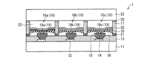
- FIG. 1 is a cross-sectional view showing a schematic configuration of a main part of the organic EL device according to the present embodiment.
- the organic EL device 1 includes an organic EL element 10 a that emits red light, an organic EL element 10 b that emits green light, and an organic EL element 10 c that emits blue light.
- the light emitting regions of the respective organic EL elements 10 are defined by partition walls (banks) 17 that are arranged in a matrix as one unit and that have conductivity.
- Each organic EL element 10 includes a lower electrode (anode) 14, a hole transport layer 18, a light emitting layer 19, an upper electrode (cathode) 20, and the like.
- a plurality of TFTs 12 for driving the organic EL element 10 are formed on the insulating substrate 11 at a predetermined interval.
- examples of the insulating substrate 11 include an inorganic material substrate made of glass or quartz, or a plastic substrate made of polyethylene terephthalate, polycarbazole, polyimide, or the like.
- the TFT 12 can be formed of a known material by a known method.
- An interlayer insulating film 13 is formed on the entire insulating substrate 11 so as to cover the TFT 12, and a lower electrode 14 made of an electrode material having a large work function is formed on the insulating substrate 11 so as to make a pair with the TFT 12. .
- a plurality of contact holes 15 are provided in the interlayer insulating film 13 according to the number of TFTs 12. In each contact hole 15, the lower electrode 14 penetrating the interlayer insulating film 13 and the TFT 12 are electrically connected. Has been.
- the interlayer insulating film 13 can be formed using a known material (inorganic material or organic material).
- inorganic material include silicon oxide (SiO 2 ), silicon nitride (SiN or Si 2 N 4 ), and tantalum oxide (TaO or Ta 2 O 5 ).
- organic material include an acrylic resin or a resist material.
- the lower electrode 14 can be formed of a known electrode material having a large work function.
- a metal such as gold (Au), platinum (Pt), nickel (Ni), an oxide (ITO) made of indium (In) and tin (Sn), an oxide of tin (Sn) (SnO 2 )
- the transparent electrode material include oxide (IZO) made of indium (In) and zinc (Zn). With these materials, injection of holes into the light emitting layer 19 described later can be made more efficient.
- a base electrode 21 for forming a partition wall 17 is provided at a predetermined interval between adjacent lower electrodes 14, and a part of each lower electrode 14 and the base electrode 21 is exposed. As described above, the edge cover 16 is formed.
- the base electrode 21 is preferably formed of the same material as the lower electrode 14 at the same time. Thereby, the base electrode 21 for forming the partition wall 17 can be formed without increasing the number of steps.
- the edge cover 16 can be formed of a known insulating material that transmits light, such as SiO, SiON, SiN, SiOC, SiC, HfSiON, ZrO, HfO, and LaO.
- a plating bank as a partition wall 17 is formed by electroplating by electrolysis of an aqueous electrolyte solution.
- the electroplating method is stipulated in JIS standard “JIS0400: 1998-1011 electroplating and related treatment terms”, and is a method of electrochemically depositing (electrodepositing) metal on a metal or non-metal surface.
- a plating bank made of copper (Cu) can be formed on each base electrode 21 by electroplating by electrolytic decomposition of an aqueous electrolyte solution into which copper sulfate or copper cyanide is injected.
- the present invention is not limited to this. It is also possible to form a plating bank including at least one of metals such as nickel (Ni), zinc (Zn), chromium (Cr), and aluminum (Al).
- the line width can be freely controlled and high definition can be supported.
- a hole transport layer 18 is formed on the edge cover 16 in each space partitioned by the partition wall 17, and a light emitting layer 19 a that emits red light as a light emitting layer 19 thereon, and emits green light.
- a light emitting layer 19b and a light emitting layer 19c that emits blue light are formed. That is, the partition wall 17 separates the light emitting layers 19 of the plurality of organic EL elements 10.
- the hole transport layer 18 can be formed of a known material.
- a known material for example, polyphylline derivatives, aromatic tertiary amine compounds, styrylamine derivatives, polyvinylcarbazole, poly-p-phenylene vinylene, polysilane, triazole derivatives, oxadiazole derivatives, imidazole derivatives, polyarylalkane derivatives, pyrazoline derivatives, pyrazolone derivatives Fluorenone derivatives, hydrogenated amorphous silicon, hydrogenated amorphous silicon carbide, zinc sulfide, and zinc selenide.
- the light emitting layer 19 has a function of deactivating energy and emitting light by recombining holes and electrons injected from both electrodes when a voltage is applied to the lower electrode 14 and the upper electrode 20. It is made of a material with high luminous efficiency.
- metal oxinoid compounds [8-hydroxyquinoline metal complexes], naphthalene derivatives, anthracene derivatives, diphenylethylene derivatives, vinylacetone derivatives, triphenylamine derivatives, butadiene derivatives, coumarin derivatives, benzoxador derivatives, oxadiazoles Derivatives, oxador derivatives, benzimidazole derivatives, thiadiazole derivatives, perylene derivatives, perinone derivatives, rhodamine derivatives, phenoxazone, quinacridone derivatives, rubrene, poly-p-phenylene vinylene, polysilane and the like.
- An upper electrode (cathode) 20 made of an electrode material having a small work function is formed on the entire insulating substrate 11 so as to cover the light emitting layer 19 and the partition wall 17. That is, the upper electrode 20 extends over the light emitting region of the light emitting layer 19 defined by the barrier ribs 17 and the barrier ribs 17 so as to be common to the plurality of organic EL elements 10.
- the upper electrode 20 and the partition wall 17 are electrically connected.
- the upper electrode 20 can be formed of a known electrode material having a small work function.
- a known electrode material having a small work function.
- Metal materials such as sodium (Na), ruthenium (Ru), manganese (Mn), indium (In), magnesium (Mg), lithium (Li), ytterbium (YB), or lithium fluoride (LiF) /
- the alloy include calcium (Ca) / aluminum (Al). With these materials, the injection of electrons into the light emitting layer 19 can be made more efficient.
- a sealing substrate 23 made of a glass substrate or the like is provided on the upper electrode 20 formed on the partition wall 17, and the upper electrode 20 and the sealing substrate 23 are applied around the sealing substrate 23. It is bonded with a sealing resin (not shown). Since the organic EL element 10 is sealed by bonding the insulating substrate 11 and the sealing substrate 23, it can be prevented from being damaged by oxygen and water. A hollow portion 22 is formed between each organic EL element 10 and the sealing substrate 23.
- the organic EL device 1 uses the lower electrode 14 and the base electrode 21 as an anode and the upper electrode 20 as a cathode.
- the base electrode 21 can be a cathode and the upper electrode 20 can be an anode.
- the laminated structure is the lower electrode (cathode) 14, the light emitting layer 19, the hole transport layer 18, and the upper electrode (anode) 20 in this order from the bottom, and used for the lower electrode 14, the base electrode 21, and the upper electrode 20. The material produced is also reversed.
- the organic EL element 10 can employ various structures. Specifically, the organic EL element 10 can be appropriately selected from the following configurations (1) to (9). In the following configurations (1) to (9), the anode and the cathode are omitted.
- the organic EL device 1 has a bottom emission structure in which light is emitted from the insulating substrate 11 side to the outside, and light is emitted from the opposite side to the insulating substrate 11 side.
- the lower electrode 14 and the base electrode 21 are made of ITO on Al.
- the upper electrode 20 may be a laminate of ITO on a translucent Ag of about 20 nm.
- Al of the lower electrode 14 and the base electrode 21 has a reflection function
- ITO has a hole injection function to the light emitting layer 19
- Ag of the upper electrode 20 has an electron injection function to the light emitting layer 19
- ITO can serve as an auxiliary electrode that lowers the resistance of the cathode.
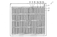
- FIG. 2 is a plan view showing a schematic configuration of a main part of the organic EL device according to the present embodiment.
- a plurality of gate lines G and a plurality of source lines S are provided so as to intersect each other.
- a pixel 30 is formed corresponding to the intersection.
- Each pixel 30 includes any one of an organic EL element 10a that emits red light, an organic EL element 10b that emits green light, and an organic EL element 10c that emits blue light.
- TFT12 is provided.
- a gate wiring G is connected to the gate electrode of the TFT 12
- a source wiring S is connected to the source electrode
- a lower electrode 14 is connected to the drain electrode
- each organic EL element 10 is connected. Is driven by the TFT 12.
- the display area of the plurality of pixels 30 is defined by a plating bank as the partition wall 17.
- FIG. 3 is a plan view showing a schematic configuration of a main part of the organic EL device according to the present embodiment.
- the organic EL device 1 includes an organic EL element 10 a that emits red light, an organic EL element 10 b that emits green light, and an organic EL element 10 c that emits blue light on an insulating substrate 11.
- the pixels 30 having either one are arranged in a matrix.
- each organic EL element 10 is formed by laminating a lower electrode 14, a hole transport layer 18, a light emitting layer 19, an upper electrode 20, and the like.
- each pixel 30 the base electrode 21 is formed of the same material as the lower electrode 14, and the partition wall 17 is formed on the base electrode 21 by electroplating. That is, each pixel 30 is surrounded by a plating bank as the partition wall 17.
- An upper electrode 20 (not shown) is formed on the entire insulating substrate 11 so as to cover the light emitting layer 19 and the partition wall 17.
- the partition wall 17 and the upper electrode 20 are electrically connected to each other, and disconnection of the upper electrode 20 by the partition wall 17 can be prevented. 20 can be reduced in resistance.
- the length of the pixel 30 is set to 450 ⁇ m
- the width is set to 150 ⁇ m
- the line width of the partition wall 17 is set to 10 ⁇ m
- the height (thickness) is set to 10 ⁇ m
- the film thickness of the upper electrode 20 is set to 200 nm.
- the partition wall 17 can be formed by electroplating a material having a higher conductivity than that of the upper electrode 20.
- the base electrode 21 is formed as a base for performing electroplating, this also has the effect of reducing the sheet resistance.
- the plating bank as the partition wall 17 has high adhesion and is difficult to peel off as compared with a conventional organic resin partition wall, damage to the organic EL element 10 due to film peeling can be suppressed.
- the electroplating method is a general-purpose method that has been practiced in various fields, and the material is not special, so that the cost can be reduced.
- the electroplating method when used, it is easy to increase the thickness of the partition wall 17, so that the organic EL element 10 and the sealing substrate 23 can be prevented from contacting each other.
- the elastic modulus is smaller than that of the organic resin partition, it can be formed with less deformation.
- Example 1 Hereinafter, the manufacturing process of the organic EL device according to the present embodiment will be described with reference to FIGS.
- FIGS. 4A to 4D are cross-sectional views showing a schematic configuration of the main part of the organic EL device according to the present embodiment.
- FIG. 5 shows the formation of the partition walls in the organic EL device according to the present embodiment. It is a figure for demonstrating the electroplating method to do.
- a plurality of TFTs 12 for driving each organic EL element 10 on an insulating substrate 11 such as a glass substrate having a length of 400 mm, a width of 320 mm, and a thickness of 0.7 mm.
- the TFT 12 can be formed using a known material by a known method.
- a photosensitive acrylic resin is applied to the entire surface of the insulating substrate 11 by spin coating, and exposure and development are performed by photolithography to form an interlayer insulating film 13 having a plurality of contact holes 15. A part of each TFT 12 is exposed through the contact hole 15.
- the exposure is performed with an exposure amount of 360 J / cm 3 and the development is performed with an alkaline developer, but the present invention is not limited to this.
- the film thickness of the interlayer insulating film 13 is preferably about 2 ⁇ m, and the diameter of each contact hole 15 is preferably about 5 ⁇ m. Thereafter, baking is performed at 220 ° C. for 1 hour.
- an ITO film having a thickness of 100 nm is formed on the entire surface of the insulating substrate 11 by sputtering, exposed and developed by photolithography, and patterned by etching.
- a lower electrode 14 is formed so as to make a pair with each TFT 12.
- the base electrode 21 is also formed from the same material as the lower electrode 14. Thereafter, baking is performed at 220 ° C. for 1 hour.
- a SiO 2 film having a thickness of 150 nm is formed on the end portions of the lower electrode 14 and the base electrode 21 by sputtering, exposed and developed by a photoresist method, and etched.
- the edge cover 16 is formed by patterning using a method. The edge cover 16 is formed so that a part of the lower electrode 14 and the base electrode 21 is exposed.
- a current is passed through the base electrode 21 to form a plating bank as the partition wall 17 by electroplating.
- a method of forming a plating bank as the partition wall 17 hangs a hooking jig 26 in a stationary tank 25 into which copper sulfate or copper cyanide is injected as an aqueous electrolyte solution.
- the base electrode 21 is hooked on the hook jig 26.
- a base electrode 21 is used as a cathode and a copper rod is used as an anode and a direct current is passed through both electrodes, copper cations are electrodeposited on the base electrode 21 only in the flowing portions, and a plating bank is formed.
- the film thickness of the plating bank as the partition wall 17 is preferably about 10 ⁇ m.
- the hole transport layer 18 and the light emitting layer 19 are formed on the edge cover 16 in each space partitioned by the partition walls 17. Further, the upper electrode 20 is formed on the entire insulating substrate 11 so as to cover the light emitting layer 19 and the partition wall 17. In addition, since the hole transport layer 18, the light emitting layer 19, and the upper electrode 20 are formed by a known process, description thereof is omitted.
- an ultraviolet curable resin or a thermosetting resin is applied to the periphery of the sealing substrate 23, and the sealing substrate 23 made of a glass substrate or the like in an inert gas atmosphere.
- the organic EL element 10 is sealed by adhering the insulating substrate 11 to each other. Thereby, a hollow portion 22 is formed between each organic EL element 10 and the sealing substrate 23. Note that a desiccant is bonded to the sealing substrate 23 in advance, and deterioration of the organic EL element 10 due to moisture can be more effectively reduced.
- the organic EL device 1 is manufactured by the above process.
- Example 2 Another embodiment relating to the organic EL device of the present invention will be described below with reference to FIG.
- the organic EL device 1 according to the present embodiment is an organic EL device having a flexible display panel.
- flexible substrates are used as the insulating substrate 11 and the sealing substrate 23.
- a plastic substrate made of polyethylene terephthalate, polyethylene naphthalate, polycarbazole, polyimide, or the like.
- the partition wall 17 when the partition wall 17 is formed of an organic resin material, it is difficult to form a thick resin film, and the film thickness is generally as low as about 2 ⁇ m. In addition, it is difficult to form a pattern having a high cross-sectional aspect ratio (height / line width), and it is desirable that the partition wall 17 formed in the non-light-emitting region be as narrow as possible.
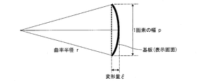
- a deformation amount ⁇ generated by rounding the display panel is defined as follows.
- FIG. 6 is a diagram for explaining a deformation amount generated by rounding the display panel in the organic EL device.
- both the substrates have an ability to bend at least by the amount described above. It is desirable. When both the substrates are bent in the same direction, the distance between the sealing substrate 23 and the insulating substrate 11 does not change. However, since both the substrates can bend in the opposite directions, in that case, the distance between the two substrates is reduced by an amount twice the amount of deformation ⁇ . That is, the distance between both substrates may be reduced by at least 5.06 ⁇ m.
- the sealing substrate 23 may come into contact with the organic EL element 10 due to deformation. When such contact occurs, the electrode material and the organic material constituting the organic EL element are damaged, so that the pixel is deteriorated and the display quality is adversely affected.
- the distance between the organic EL element 10 and the sealing substrate 23 it is necessary to set the distance between the organic EL element 10 and the sealing substrate 23 to a value that does not contact. Further, in view of temporary deformation exceeding the normal curvature radius and local strong deformation caused by pressing, it is desirable to make the distance between the organic EL element 10 and the sealing substrate 23 wider.
- the partition wall 17 is formed of an organic resin material as in the prior art, a number of problems occur, and it cannot be applied to an organic EL device having a flexible panel.
- a plating bank is formed as the partition wall 17, it is possible to form a pattern with a high cross-sectional aspect ratio (height / line width), which is suitable for an organic EL device having a flexible display panel. It is.
- the organic EL device 2 according to the present embodiment has the same configuration as the organic EL device 1 according to the first embodiment shown in FIG. However, the formation method of the partition wall 17 is different. That is, in the first embodiment, the partition wall 17 is formed by electroplating, but in this embodiment, the partition wall 17 is formed by electroless plating.
- a plating bank as the partition wall 17 is formed on each base electrode 21 by electroless plating.
- the electroless plating method is defined in the JIS standard “JIS 0400: 1998-6001, electroless plating and related processing terms”, and is a method of chemically reducing and depositing a metal without using an external power source.
- a plating bank made of copper (Cu) can be formed on each base electrode 21 by an electroless plating method based on a reduction reaction in a solution into which copper sulfate or copper cyanide is injected.
- a plating bank including at least one of metals such as nickel (Ni), zinc (Zn), chromium (Cr), and aluminum (Al).
- FIG. 7 are cross-sectional views showing a schematic configuration of a main part of the organic EL device 2 according to this example.
- a plurality of TFTs 12 for driving each organic EL element 10 on an insulating substrate 11 such as a glass substrate having a length of 400 mm, a width of 320 mm, and a thickness of 0.7 mm.
- the TFT 12 can be formed using a known material by a known method.
- a photosensitive acrylic resin is applied to the entire surface of the insulating substrate 11 by spin coating, and exposure and development are performed by photolithography to form an interlayer insulating film 13 having a plurality of contact holes 15. A part of each TFT 12 is exposed through the contact hole 15.
- the exposure is performed with an exposure amount of 360 J / cm 3 and the development is performed with an alkaline developer, but the present invention is not limited to this.
- the film thickness of the interlayer insulating film 13 is preferably about 2 ⁇ m, and the diameter of each contact hole 15 is preferably about 5 ⁇ m. Thereafter, baking is performed at 220 ° C. for 1 hour.
- an ITO film having a thickness of 100 nm is formed on the entire surface of the insulating substrate 11 by sputtering, exposed and developed by photolithography, and patterned by etching.
- a lower electrode 14 is formed so as to make a pair with each TFT 12.
- the base electrode 21 is also formed from the same material as the lower electrode 14. Thereafter, baking is performed at 220 ° C. for 1 hour.
- a SiO 2 film having a thickness of 150 nm is formed on the end portions of the lower electrode 14 and the base electrode 21 by sputtering, exposed and developed by a photoresist method, and etched.
- the edge cover 16 is formed by patterning using a method. The edge cover 16 is formed so that a part of the lower electrode 14 and the base electrode 21 is exposed.
- a resist film 31 is applied on the entire surface of the substrate by spin coating, exposed and developed by photolithography, and patterned so that a part of the base electrode 21 is exposed. Do.
- the electroless plating method is immersed in a solution into which copper sulfate or copper cyanide is injected in the same manner as the electroplating method, and the copper film 32 is formed on the entire surface of the substrate. Form.
- the resist film 31 is peeled off, as shown in FIG.
- the copper film as the partition wall 17 is left only on the lower electrode 21.
- a hole transport layer 18 and a light emitting layer 19 are formed on the edge cover 16 in each space partitioned by the partition walls 17. Further, the upper electrode 20 is formed on the entire insulating substrate 11 so as to cover the light emitting layer 19 and the partition wall 17.
- the hole transport layer 18, the light emitting layer 19, and the upper electrode 20 can be formed by a known process, description thereof is omitted here.
- an ultraviolet curable resin or a thermosetting resin is applied to the periphery of the sealing substrate 23, and the sealing substrate 23 made of a glass substrate or the like and the insulating substrate 11 are bonded in an inert gas atmosphere to thereby form an organic material.
- the EL element 10 is encapsulated. Thereby, a hollow portion 22 is formed between each organic EL element 10 and the sealing substrate 23. Note that a desiccant is bonded to the sealing substrate 23 in advance, and deterioration of the organic EL element 10 due to moisture can be more effectively reduced.
- the organic EL device 2 is manufactured by the above process.
- the organic EL device of the present invention is It is preferable that the partition includes at least one of Cu, Ni, Zn, Cr, and Al.
- the organic EL device of the present invention is It is preferable that a sealing substrate is formed on the upper electrode.
- the organic EL element can be prevented from being damaged by oxygen and water.
- the organic EL device of the present invention is The partition is preferably formed by electroplating.
- the partition wall has higher adhesion to the base and is less likely to be peeled off than a partition wall made of a conventional organic resin, so that damage to the organic EL element due to film peeling can be suppressed.
- the electroplating method is a general-purpose method that has been practiced in various fields, and can reduce the cost.
- the organic EL device of the present invention is Further comprising a base electrode made of the same material as the lower electrode,
- the partition is preferably formed on the base electrode.
- the partition wall is formed only on the base electrode, the line width of the partition wall can be freely controlled, and the pixel aperture ratio is not reduced, and high definition can be achieved.
- the base electrode is produced at the same time as the lower electrode of the organic EL device, the number of processes does not increase.
- the present invention can be applied to an organic EL device.
- a thick film partition can be easily formed, it is most suitable for a flexible organic EL device in which a collision easily occurs due to bending or pressing force.
Landscapes
- Engineering & Computer Science (AREA)
- Microelectronics & Electronic Packaging (AREA)
- Physics & Mathematics (AREA)
- Optics & Photonics (AREA)
- Electroluminescent Light Sources (AREA)
Abstract
有機EL装置(1)は、基板(11)と、基板(11)上に、発光領域のそれぞれに対応して形成された複数の下部電極(14)と、発光領域のそれぞれを取り囲むように形成された隔壁(17)と、発光領域のそれぞれにおいて、下部電極(14)上に形成された発光層(19)と、隔壁(17)上及び発光層(19)上に形成された上部電極(20)とを備え、隔壁(17)は、導電性を有するとともに、上部電極(20)と電気的に接続されている。
Description
本発明は、有機EL装置、電子機器及び有機EL装置の製造方法に関するものであり、特にフレキシブル(柔軟)な有機EL装置、電子機器及び有機EL装置の製造方法に関するものである。
近年、高度情報化に伴い、フラットパネルディスプレイに対する需要が高まっている。このようなディスプレイとして、非自発光型の液晶ディスプレイ(LCD)、自発光型のプラズマディスプレイ(PDP)、無機エレクトロルミネセンス(無機EL)ディスプレイ、および有機エレクトロルミネセンス(有機EL)ディスプレイ(例えば、特許文献1)等が知られている。この中でも、有機ELディスプレイは、自発光型のディスプレイであり、視野角が広い、コントラストが高い、応答速度が速い等、LCDにない特長を有しており、特に注目されている。
以下、有機ELディスプレイ等の電子機器に適用される一般的な有機EL装置について、図8を用いて説明する。図8は、従来の有機EL装置の要部の構成を概略的に示す断面図である。
図8に示すように、有機EL装置100には、有機EL素子110として、赤色光を発光する有機EL素子110a、緑色光を発光する有機EL素子110bおよび青色光を発光する有機EL素子110cが1単位として、マトリクス状に配列されており、隔壁(バンク)117により、各有機EL素子110の発光領域が画定されている。なお、各有機EL素子110は、下部電極(陽極)114、正孔輸送層118、発光層119、上部電極(陰極)120等から構成されている。
より具体的には、有機EL装置100には、ガラス基板等からなる絶縁基板111上に、駆動素子としてのTFT(Thin Film Transistor:薄膜トランジスタ)112が複数形成されている。このTFT112を覆うように、絶縁基板111全体に、酸化シリコン(SiO2)、窒化シリコン(SiN)等からなる層間絶縁膜113が形成されており、その上に、仕事関数の大きな電極材料、例えばITO(Indium Tin Oxide:インジウムスズ酸化物)やIZO(Indium Zinc Oxide:酸化インジウム・酸化亜鉛)等からなる下部電極114がTFT112と対をなすように形成されている。なお、層間絶縁膜113には、TFT112の数に応じて複数のコンタクトホール115が設けられており、各コンタクトホール115において、層間絶縁膜113を貫通する下部電極114と、TFT112とが電気的に接続されている。
隣り合う下部電極114の境界部分を覆うように、酸化シリコン(SiO2)等絶縁材料からなるエッジカバー116が複数形成されており、その上に、アクリル樹脂等有機樹脂材料からなる隔壁117が形成されている。なお、隔壁117は、アクリル材料をスピンコートにて塗布し、フォトリソグラフィ法で露光、現像を行って形成したものである。
隔壁117で区画された各空間内のエッジカバー116上に、例えば、酸化バナジウム(V2O5)および酸化モリブデン(MoO2)等の酸化物からなる正孔輸送層118が形成されており、その上に、発光層119として、公知の有機発光材料からなる赤色光を発光する発光層119a、緑色光を発光する発光層119b、青色光を発光する発光層119cがそれぞれ形成されている。即ち、隔壁117は、複数の有機EL素子110の発光層119を区分している。
発光層119及び隔壁117を覆うように、絶縁基板111の全体に上部電極(陰極)120が形成されている。つまり、上部電極120は、複数の有機EL素子110に共通するように、隔壁117で画定された発光層119の区域および隔壁117上に広がっている。
上部電極120上には、封止樹脂121が接着されており、その上にガラス基板等からなる封止基板122が設けられている。このように、有機EL素子110は、絶縁基板111と封止基板122との貼り合わせにより封入されている。この構成により、有機EL素子110が酸素及び水でダメージを受けることを防止できる。
このような有機EL装置100では、隔壁117が有機樹脂材料で形成されているため、これに起因する種々の問題が生じる。
先ず、有機樹脂材料は絶縁体であるため、隔壁117を覆う上部電極120に断線が発生する可能性がある。
また、有機樹脂膜は、一般的にスパッタ(Sputter)膜やCVD(Chemical Vapor Deposition)膜に比べて、下地(SiO2等)との密着性が低いため、有機樹脂材料からなる隔壁117は、剥がれやすく、有機EL素子110に損傷を与える可能性がある。
また、有機樹脂材料からなる隔壁117を形成する方法としては、フォトリソグラフィ法が挙げられるが、これは感光性のフォトレジストを露光、現像および焼成することで、所望の高さをもつパターン膜を形成する方法である。しかしながら、この方法を利用した場合、厚いフォトレジスト樹脂膜を形成することが材料的に困難であり、一般的にその膜厚は1~4μmと低く、また、フォトレジスト樹脂膜は焼成後も高い弾性率を有しているため、表示パネルを丸めたり、押圧したりすると、衝突が発生する虞がある。
具体的には、有機EL素子110は、上述したように絶縁基板111と封止基板122との貼り合わせにより封止されているが、封止方法としては、封止基板122周辺に塗られた封止樹脂にて有機EL素子110全体を封止する方法や、図8に示すように、絶縁基板111と封止基板122との間に充填された封止樹脂あるいは接着剤により両基板を貼り合わせることにより有機EL素子110毎に封止する方法等がある。このうち、前者の方法では、有機EL素子110上に中空部が形成されることになる。この中空部の幅、すなわち有機EL素子110と封止基板122との距離が充分でないと、有機EL装置100に押圧が加わったり、屈曲が発生した場合に、絶縁基板111や封止基板122が変形し、中空部内の有機EL素子110と封止基板122とが接触し、衝突が発生する虞がある。衝突が発生すると、有機EL素子110が損傷し、表示性能に悪影響を与える虞がある。また、後者の方法においては、絶縁基板111と封止基板122との間に封止樹脂あるいは接着剤が充填されているために、両基板の直接の接触は発生しない。しかしながら、その一方で、有機EL装置100に押圧が加わったり、屈曲が発生した場合には、封止基板122の押圧や応力が封止樹脂あるいは接着剤を介して有機EL素子110に伝達されることになる。加えて、封止樹脂あるいは接着剤自体の応力も有機EL素子110に伝達される。さらには、両基板、封止樹脂あるいは接着剤の熱膨張係数の差によっても応力が発生し、それが有機EL素子110に伝達される。有機EL素子110に加えられた押圧や応力は有機EL素子110を損傷させ、表示性能に悪影響を与える虞がある。高いフレキシブル性を有する有機EL装置100においては、後者の封止方法はより深刻な問題となる。
なお、上述のように、一般的に厚いフォトレジスト樹脂膜を形成することが材料的に困難であるが、例えば、膜厚10μmの厚いフォトレジスト樹脂膜を形成することができるフォトレジストがあったとしても、特殊な材料に限られ、高価なものとなり、有機EL装置100の高コスト化に繋がる。
さらに、断面アスペクト比(高さ÷線幅)の高いフォトレジスト樹脂膜を形成することが材料的に困難である。よって、所定の高さのフォトレジスト樹脂膜を形成しようとすると、線幅を広くする必要があるため、画素の開口率が低下し、高精細化が実現できなくなる。例えば、隔壁117の高さを10μmと設定し、線幅を10μmと設定した場合、断面アスペクト比は1が必要となる。この断面アスペクト比を実現することは一般的には難しく、仮に、該断面アスペクト比を達成するフォトレジストがあったとしても、特殊な材料に限られ、高価なものとなり、有機EL装置100の高コスト化に繋がる。また、断面アスペクト比を高くしたまま、10μm等の厚いフォトレジスト樹脂膜を形成するためには、垂直に近いテーパをもつフォトレジストが必要である。ここで、テーパとは、フォトレジストの側面が基板と成す角度のことを示し、90度未満を順テーパ、90度を越える場合を逆テーパと称する。順テーパや逆テーパの場合には、天井部または底部に行くほど線幅が細くなってしまうため、所望の高さと線幅を得ることは難しい。そこで、垂直に近いテーパをもつフォトレジストが用いられているが、上部電極120の蒸着時に、フォトレジスト側面には付着する量が少ないため、上部電極120は、隔壁117の側面で断線が発生しやすい。
このように、従来の有機EL装置では、隔壁が樹脂製であることに起因する種々の問題が生じる。
本発明は、上記の問題点に鑑みてなされたものであり、その目的は、断線が発生しにくく、信頼性が高い有機EL装置、電子機器、及び有機EL装置の製造方法を提供することにある。
さらには、低コスト化、高精細化が可能な有機EL装置、電子機器、及び有機EL装置の製造方法を提供することにある。
上記の課題を解決するために、本発明の有機EL装置は、
複数の発光領域を有する有機EL装置であって、
基板と、
前記基板上に、前記発光領域のそれぞれに対応して形成された複数の下部電極と、
前記発光領域のそれぞれを取り囲むように形成された隔壁と、
前記発光領域のそれぞれにおいて、前記下部電極上に形成された発光層と、
前記隔壁上及び前記発光層上に形成された上部電極と、を備え、
前記隔壁は、導電性を有するとともに、前記上部電極と電気的に接続されていることを特徴とする。
複数の発光領域を有する有機EL装置であって、
基板と、
前記基板上に、前記発光領域のそれぞれに対応して形成された複数の下部電極と、
前記発光領域のそれぞれを取り囲むように形成された隔壁と、
前記発光領域のそれぞれにおいて、前記下部電極上に形成された発光層と、
前記隔壁上及び前記発光層上に形成された上部電極と、を備え、
前記隔壁は、導電性を有するとともに、前記上部電極と電気的に接続されていることを特徴とする。
上記構成によれば、隔壁及び上部電極は、互いに電気的に接続されているため、隔壁による上部電極の断線を防止することができ、また、上部電極の低抵抗化を図ることができる。
よって、断線が発生しにくく、信頼性が高い有機EL装置を提供することができる。
本発明の電子機器は、
前記有機EL装置を備えていることを特徴とする。
前記有機EL装置を備えていることを特徴とする。
よって、断線が発生しにくく、信頼性が高い電子機器を提供することができる。
本発明の有機EL装置の製造方法は、
複数の発光領域を有する有機EL装置の製造方法であって、
基板上に前記発光領域のそれぞれに対応して複数の下部電極を形成するとともに、これと同時に、隣り合う下部電極の間に、前記下部電極と同一材料の下地電極を形成する工程と、
前記発光領域のそれぞれを取り囲むように、前記下地電極上に電気めっき法により隔壁を形成する工程と、
前記発光領域のそれぞれにおいて、前記下部電極上に発光層を形成する工程と、
前記隔壁上及び前記発光層上に、該隔壁と電気的に接続されるように上部電極を形成する工程と、
を含むことを特徴とする。
複数の発光領域を有する有機EL装置の製造方法であって、
基板上に前記発光領域のそれぞれに対応して複数の下部電極を形成するとともに、これと同時に、隣り合う下部電極の間に、前記下部電極と同一材料の下地電極を形成する工程と、
前記発光領域のそれぞれを取り囲むように、前記下地電極上に電気めっき法により隔壁を形成する工程と、
前記発光領域のそれぞれにおいて、前記下部電極上に発光層を形成する工程と、
前記隔壁上及び前記発光層上に、該隔壁と電気的に接続されるように上部電極を形成する工程と、
を含むことを特徴とする。
上記製造方法によれば、隔壁及び上部電極は、互いに電気的に接続されているため、隔壁による上部電極の断線を防止することができ、また、上部電極の低抵抗化を図ることができる。
また、隔壁は、従来の有機樹脂からなる隔壁と比較して、下地との密着性が高く剥がれにくいため、膜剥がれによる有機EL素子の損傷を抑制することができる。
また、隔壁の厚膜化が容易になるため、有機EL素子と封止基板が接触することを防止することができ、弾性率も有機樹脂の隔壁と比較して小さいため、変形し難くすることができる。よって、有機EL素子の損傷を抑制することができる。
また、電気めっき法は、従来から多方面で実施されている汎用の手法であり、低コスト化が可能である。
また、隔壁は下地電極上のみに形成されるため、隔壁の線幅を自由に制御でき、画素開口率の低下に繋がらなく、高精細化を実現することができる。
本発明の有機EL装置は、複数の発光領域を有する有機EL装置であって、基板と、前記基板上に、前記発光領域のそれぞれに対応して形成された複数の下部電極と、前記発光領域のそれぞれを取り囲むように形成された隔壁と、前記発光領域のそれぞれにおいて、前記下部電極上に形成された発光層と、前記隔壁上及び前記発光層上に形成された上部電極と、を備え、前記隔壁は、導電性を有するとともに、前記上部電極と電気的に接続されていることを特徴とする。
また、本発明の電子機器は、前記有機EL装置を備えていることを特徴とする。
また、本発明の有機EL装置の製造方法は、複数の発光領域を有する有機EL装置の製造方法であって、基板上に前記発光領域のそれぞれに対応して複数の下部電極を形成するとともに、これと同時に、隣り合う下部電極の間に、前記下部電極と同一材料の下地電極を形成する工程と、前記発光領域のそれぞれを取り囲むように、前記下地電極上に電気めっき法により隔壁を形成する工程と、前記発光領域のそれぞれにおいて、前記下部電極上に発光層を形成する工程と、前記隔壁上及び前記発光層上に、該隔壁と電気的に接続されるように上部電極を形成する工程と、を含むことを特徴とする。
それゆえ、断線が発生しにくく、信頼性が高い有機EL装置、電子機器、及び有機EL装置の製造方法を提供することができる。
以下、本発明の実施の形態について、詳細に説明する。
〔実施の形態1〕
本発明の一実施の形態について、図面に基づいて説明すれば以下のとおりである。本発明に係る有機EL装置は、テレビ用ディスプレイ、携帯電話機用ディスプレイ、PC用ディスプレイ等の種々の電子機器に適用することができるものである。
本発明の一実施の形態について、図面に基づいて説明すれば以下のとおりである。本発明に係る有機EL装置は、テレビ用ディスプレイ、携帯電話機用ディスプレイ、PC用ディスプレイ等の種々の電子機器に適用することができるものである。
(有機EL装置の断面構成)
先ず、図1に基づいて本実施の形態に係る有機EL装置の断面構成について説明する。
先ず、図1に基づいて本実施の形態に係る有機EL装置の断面構成について説明する。
図1は、本実施の形態に係る有機EL装置の要部の概略構成を示す断面図である。
図1に示すように、有機EL装置1には、有機EL素子10として、赤色光を発光する有機EL素子10a、緑色光を発光する有機EL素子10bおよび青色光を発光する有機EL素子10cが1単位として、マトリクス状に配列されており、導電性を有する隔壁(バンク)17により、各有機EL素子10の発光領域が画定されている。なお、各有機EL素子10は、下部電極(陽極)14、正孔輸送層18、発光層19、上部電極(陰極)20等から構成されている。
より具体的には、有機EL装置1には、絶縁基板11上に、有機EL素子10を駆動するための複数のTFT12が所定の間隔で形成されている。
ここで、絶縁基板11としては、例えば、ガラスまたは石英等からなる無機材料基板、または、ポリエチレンテレフタレート、ポリカルバゾール、またはポリイミド等からなるプラスティック基板等が挙げられる。
また、TFT12は、公知の材料を公知の方法によって形成することができる。
このTFT12を覆うように、絶縁基板11全体に、層間絶縁膜13が形成されており、その上に、仕事関数の大きな電極材料からなる下部電極14がTFT12と対をなすように形成されている。層間絶縁膜13には、TFT12の数に応じて複数のコンタクトホール15が設けられており、各コンタクトホール15おいて、層間絶縁膜13を貫通する下部電極14と、TFT12とが電気的に接続されている。
ここで、層間絶縁膜13は、公知の材料(無機材料または有機材料)を用いて形成することができる。無機材料として、例えば、酸化シリコン(SiO2)、窒化シリコン(SiN、又は、Si2N4)、または酸化タンタル(TaOまたはTa2O5)等が挙げられる。有機材料として、アクリル樹脂またはレジスト材料等が挙げられる。
また、下部電極14は、公知の仕事関数の大きな電極材料によって形成することができる。例えば、金(Au)、白金(Pt)、ニッケル(Ni)等の金属、および、インジウム(In)と錫(Sn)からなる酸化物(ITO)、錫(Sn)の酸化物(SnO2)インジウム(In)と亜鉛(Zn)からなる酸化物(IZO)等が透明電極材料として挙げられる。これらの材料なら、後述する発光層19への正孔の注入をより効率化できる。
層間絶縁膜13上には、隣り合う下部電極14の間に、隔壁17を形成するための下地電極21が所定の間隔で設けられており、各下部電極14及び下地電極21の一部が露出されるようにエッジカバー16が形成されている。
ここで、下地電極21は、下部電極14と同時に同じ材料で形成することが好ましい。これにより、工程を増加することがなく、隔壁17を形成するための下地電極21を形成することができる。
また、エッジカバー16は、光を透過する公知の絶縁材料、例えば、SiO、SiON、SiN、SiOC、SiC、HfSiON、ZrO、HfO、およびLaO等により形成することができる。
各下地電極21上には、電解質水溶液の電気分解による電気めっき法で、隔壁17としてのメッキバンクが形成されている。ここで、電気めっき法は、JIS規格『JISH0400:1998-1011 電気めっき及び関連処理用語』において規定されており、金属または非金属表面に金属を電気化学的に析出(電着)させる方法である。例えば、硫酸銅、またはシアン化銅が注入された電解質水溶液の電解分解による電気めっき法で、各下地電極21上に、銅(Cu)からなるメッキバンクを形成することができるが、これに限定されることなく、ニッケル(Ni)、亜鉛(Zn)、クロム(Cr)、アルミニウム(Al)等の金属から少なくとも何れかを含んでメッキバンクを形成することもできる。
隔壁17は、下地電極21上に、電気めっき法で形成されているため、線幅を自由に制御でき、高精細化に対応が可能である。
隔壁17で区画された各空間内のエッジカバー16上に、正孔輸送層18が形成されており、その上に、発光層19として、赤色光を発光する発光層19a、緑色光を発光する発光層19b、青色光を発光する発光層19cがそれぞれ形成されている。即ち、隔壁17は、複数の有機EL素子10の発光層19を区分している。
ここで、正孔輸送層18は、公知の材料で形成することができる。例えば、ポリフィリン誘導体、芳香族第三級アミン化合物、スチリルアミン誘導体、ポリビニルカルバゾール、ポリ-p-フェニレンビニレン、ポリシラン、トリアゾール誘導体、オキサジアゾール誘導体、イミダゾール誘導体、ポリアリールアルカン誘導体、ピラゾリン誘導体、ピラゾロン誘導体、フルオレノン誘導体、水素化アモルファスシリコン、水素化アモルファス炭化シリコン、硫化亜鉛、セレン化亜鉛が挙げられる。
また、発光層19は、下部電極14と上部電極20に電圧を印加した時に、両電極から注入される正孔および電子を再結合して、エネルギーを失活し、光を出射する機能を有しており、発光効率が高い材料で形成されている。具体的には、金属オキシノイド化合物[8-ヒドロキシキノリン金属錯体]、ナフタレン誘導体、アントラセン誘導体、ジフェニルエチレン誘導体、ビニルアセトン誘導体、トリフェニルアミン誘導体、ブタジエン誘導体、クマリン誘導体、ベンズオキサドール誘導体、オキサジアゾール誘導体、オキサドール誘導体、ベンズイミダゾール誘導体、チアジアゾール誘導体、ペリレン誘導体、ペリノン誘導体、ローダミン誘導体、フェノキサゾン、キナクリドン誘導体、ルブレン、ポリーp-フェニレンビニレン、ポリシラン等が挙げられる。
発光層19及び隔壁17を覆うように、絶縁基板11の全体に、仕事関数の小さな電極材料からなる上部電極(陰極)20が形成されている。つまり、上部電極20は、複数の有機EL素子10に共通するように、隔壁17で画定された発光層19の発光領域および隔壁17上に広がっている。なお、上部電極20と隔壁17とは電気的に接続されている。
ここで、上部電極20は、公知の仕事関数の小さな電極材料によって形成することができる。例えば、銀(Ag)、アルミニウム(Al)、バナジウム(V)、コバルト(Co)ニッケル(Ni)、タングステン(W)、金(Au)、カルシウム(Ca)、チタン(Ti)、イットリウム(Y)、ナトリウム(Na)、ルテニウム(Ru)、マンガン(Mn)、インジウム(In)、マグネシウム(Mg)、リチウム(Li)、イッテルビウム(YB)、等の金属材料、または、フッ化リチウム(LiF)/カルシウム(Ca)/アルミニウム(Al)等の合金が挙げられる。これらの材料なら、発光層19への電子の注入をより効率化できる。
隔壁17上に形成された上部電極20上には、ガラス基板等からなる封止基板23が設けられており、上部電極20と封止基板23とは、封止基板23の周辺に塗られた封止樹脂(図示せず)にて接着されている。有機EL素子10は、絶縁基板11と封止基板23との貼り合わせにより封入されているため、酸素及び水でダメージを受けることを防止できる。なお、各有機EL素子10と封止基板23との間には中空部22が形成されている。
本実施の形態においては、有機EL装置1は、下部電極14及び下地電極21を陽極と、上部電極20を陰極としているが、これに限定されることなく、積層構造を反転し、下部電極14及び下地電極21を陰極と、上部電極20を陽極とすることもできる。この場合、積層構造としては、下部より下部電極(陰極)14、発光層19、正孔輸送層18、上部電極(陽極)20の順になり、下部電極14と下地電極21及び上部電極20に用いられる材料も逆転する。例えば、下部電極14及び下地電極21を陰極として仕事関数の小さなAl(アルミニウム)を用い、上部電極20を陽極として仕事関数の大きなITOを用いることができる。さらには、求められる特性に応じて、有機EL素子10に、正孔注入層、電子輸送層や電子注入層を積層構造に適宜追加することもできる。また、正孔輸送層が正孔注入層を兼ねていてもよい。このように、有機EL素子10は、種々の構造を採用することができる。具体的には、有機EL素子10は、下記の構成(1)~(9)で適宜選択することが可能である。下記の各構成(1)~(9)において、陽極および陰極は省略している。
(1)発光層
(2)正孔輸送層/発光層
(3)発光層/電子輸送層
(4)正孔輸送層/発光層/電子輸送層
(5)正孔注入層/正孔輸送層/発光層/電子輸送層
(6)正孔注入層/正孔輸送層/発光層/電子輸送層/電子注入層
(7)正孔注入層/正孔輸送層/発光層/正孔防止層/電子輸送層
(8)正孔注入層/正孔輸送層/発光層/正孔防止層/電子輸送層/電子注入層
(9)正孔注入層/正孔輸送層/電子防止層/発光層/正孔防止層/電子輸送層/電子注入層
また、有機EL装置1は、絶縁基板11側から光を外部に放出するボトムエミッション構造、絶縁基板11側とは反対側から光を外部に放出するトップエミッション構造のどちらかの構造を採用することもできる。但し、トップエミッション構造の場合、下部電極14及び下地電極21にて光を反射し、上部電極20から光を取り出す必要があるため、例えば、下部電極14と下地電極21として、Alの上にITOを積層したものを用い、上部電極20として20nm程度の半透明のAgの上にITOを積層したものを用いてもよい。この場合、下部電極14及び下地電極21のAlは反射機能を担い、ITOは発光層19への正孔注入機能を担うと共に、上部電極20のAgは発光層19への電子注入機能を担い、ITOは陰極の抵抗を下げる補助電極としての機能を担うことができる。
(1)発光層
(2)正孔輸送層/発光層
(3)発光層/電子輸送層
(4)正孔輸送層/発光層/電子輸送層
(5)正孔注入層/正孔輸送層/発光層/電子輸送層
(6)正孔注入層/正孔輸送層/発光層/電子輸送層/電子注入層
(7)正孔注入層/正孔輸送層/発光層/正孔防止層/電子輸送層
(8)正孔注入層/正孔輸送層/発光層/正孔防止層/電子輸送層/電子注入層
(9)正孔注入層/正孔輸送層/電子防止層/発光層/正孔防止層/電子輸送層/電子注入層
また、有機EL装置1は、絶縁基板11側から光を外部に放出するボトムエミッション構造、絶縁基板11側とは反対側から光を外部に放出するトップエミッション構造のどちらかの構造を採用することもできる。但し、トップエミッション構造の場合、下部電極14及び下地電極21にて光を反射し、上部電極20から光を取り出す必要があるため、例えば、下部電極14と下地電極21として、Alの上にITOを積層したものを用い、上部電極20として20nm程度の半透明のAgの上にITOを積層したものを用いてもよい。この場合、下部電極14及び下地電極21のAlは反射機能を担い、ITOは発光層19への正孔注入機能を担うと共に、上部電極20のAgは発光層19への電子注入機能を担い、ITOは陰極の抵抗を下げる補助電極としての機能を担うことができる。
(有機EL装置の平面構成)
以下、図2に基づいて本実施の形態に係る有機EL装置の平面構成について説明する。
以下、図2に基づいて本実施の形態に係る有機EL装置の平面構成について説明する。
図2は、本実施の形態に係る有機EL装置の要部の概略構成を示す平面図である。
図2に示すように、有機EL装置1の表示領域において、複数のゲート配線G及び複数のソース配線Sとが互いに交差するように設けられており、各ゲート配線Gと各ソース配線Sとの交点に対応して、画素30が形成されている。
なお、各画素30は、赤色光を発光する有機EL素子10a、緑色光を発光する有機EL素子10bおよび青色光を発光する有機EL素子10cのいずれかを備えており、また、駆動用素子としてのTFT12を備えている。このTFT12のゲート電極には、ゲート配線Gが接続されており、ソース電極には、ソース配線Sが接続されており、ドレイン電極には、下部電極14が接続されており、各有機EL素子10は、TFT12により駆動される。
また、複数の画素30は、隔壁17としてのメッキバンクにより表示領域が画定されている。
(隔壁の構成)
以下、図3に基づいて本実施の形態に係る有機EL装置において、隔壁の構成についてさらに詳細に説明する。
以下、図3に基づいて本実施の形態に係る有機EL装置において、隔壁の構成についてさらに詳細に説明する。
図3は、本実施の形態に係る有機EL装置の要部の概略構成を示す平面図である。
図3に示すように、有機EL装置1には、絶縁基板11上に、赤色光を発光する有機EL素子10a、緑色光を発光する有機EL素子10b、青色光を発光する有機EL素子10cのいずれかを備えている画素30がマトリクス状に配列されている。なお、各有機EL素子10は、図1に示すように、下部電極14、正孔輸送層18、発光層19、上部電極20等が積層して構成されている。
各画素30の間には、下地電極21が下部電極14と同時に、同じ材料で形成されており、この下地電極21上には、電気めっき法により、隔壁17が形成されている。即ち、各画素30は、隔壁17としてのメッキバンクにより囲まれている。
発光層19及び隔壁17を覆うように、絶縁基板11の全体に、上部電極20(図示せず)が形成されている。
ここで、上述したように、電気めっき法により、隔壁17が形成されているため、以下の効果を奏する。
先ず、隔壁17としてのメッキバンクは、導電性を有しているため、隔壁17及び上部電極20は互いに電気的に接続され、隔壁17による上部電極20の断線を防止することができ、上部電極20の低抵抗化を図ることができる。例えば、画素30の長さを450μm、広さを150μm、隔壁17の線幅を10μm、高さ(厚み)を10μm、上部電極20の膜厚を200nmに設定し、隔壁17の導電率を上部電極20と同じように設定すると、隔壁17の高さは、上部電極20の膜厚の50倍、面積は1.78×10⁻³になるため、隔壁17のシート抵抗は、上部電極20のおよそ11倍になる。隔壁17と上部電極20とが並列に接続されることになるため、シート抵抗は11/12=0.92倍に低下する。なお、トップエミッション構造のように、上部電極20が薄い構造においては、さらに顕著な抵抗低減効果が生じる。例えば、上部電極20の膜厚を20nmに設定すると、シート抵抗は0.53倍に低下する。また、隔壁17の高さや線幅を増やすことにより、さらにシート抵抗を低減することができる。なお、同一の膜厚を得ようとする場合、電気めっきによる処理は、蒸着よりも遥かに短く、隔壁17の厚みを増やすことは容易である。また、隔壁17は、上部電極20よりも高導電率の材料を電気めっきで形成することも可能である。また、電気めっきを行うために、下地として下地電極21を形成しているため、これもシート抵抗を下げる効果を奏する。
また、隔壁17としてのメッキバンクは、従来の有機樹脂の隔壁と比較して、密着性が高く剥がれにくいため、膜剥がれによる有機EL素子10の損傷を抑制できる。
また、電気めっき法は、従来から多方面で実施されている汎用の手法であり、材料も特別なものではないので、低コスト化が可能である。
また、電気めっき法を利用すると、隔壁17の厚膜化が容易になるため、有機EL素子10と封止基板23が接触することを防止することができる。また、弾性率も有機樹脂の隔壁と比較して小さいため、変形し難く形成することができる。
以下、本発明の具体的な実施例に基づいて本実施の形態をさらに詳細に説明する。しかしながら、本発明はこれらの例に限定されない。説明の便宜上、実施の形態において説明した部材と同じ機能を有する部材については、各実施例においても同じ符号を付記する。
(実施例1)
以下、図4、図5に基づいて、本実施例に係る有機EL装置の製造プロセスについて説明する。
以下、図4、図5に基づいて、本実施例に係る有機EL装置の製造プロセスについて説明する。
図4の(a)~(d)は、本実施例に係る有機EL装置の要部の概略構成を示す断面図であり、図5は、本実施例に係る有機EL装置において、隔壁を形成する電気めっき法を説明するための図である。
先ず、図4の(a)に示すように、長さ400mm、広さ320mm、厚さ0.7mmのガラス基板等の絶縁基板11上に、各有機EL素子10を駆動するための複数のTFT12を所定の間隔で形成する。なお、TFT12は、公知の材料を公知の方法で形成することができる。その後、絶縁基板11の全面に、スピンコート法にて感光性のアクリル樹脂を塗布し、フォトリソグラフィ法により露光、現像を行い、複数のコンタクトホール15を備えた層間絶縁膜13を形成する。このコンタクトホール15により、各TFT12の一部が露出される。本実施例においては、露光量360J/cm3にて露光を行い、アルカリ現像液にて現像を行っているが、これに限定されない。層間絶縁膜13の膜厚は2μm程度、各コンタクトホール15の径は5μm程度が好ましい。その後、220℃で、1時間の焼成を行う。
次に、図4の(b)に示すように、絶縁基板11の全面に、スパッタ法にてITO膜を100nm成膜し、フォトリソグラフィ法により露光、現像を行い、エッチング法によりパターニングを行い、各TFT12と対をなすように下部電極14を形成する。なお、各コンタクトホール15において、層間絶縁膜13を貫通する下部電極14とTFT12とは電気的に接続される。同時に、下部電極14と同じ材料で下地電極21も形成する。その後、220℃で、1時間の焼成を行う。
次に、図4の(b)に示すように、下部電極14と下地電極21の端部に、スパッタ法にてSiO2膜を150nm成膜し、フォトレジスト法により露光、現像を行い、エッチング法を用いてパターンニングを行い、エッジカバー16を形成する。なお、エッジカバー16は、下部電極14及び下地電極21の一部が露出されるように形成する。
次に、図4の(b)に示すように、下地電極21に電流を流し、電気めっき法にて、隔壁17としてのメッキバンクを形成する。
隔壁17としてのメッキバンクを形成する方法は、具体的には、図5に示すように、電解質水溶液として硫酸銅、またはシアン化銅が注入された静止槽25に、引掛け治具26を吊るし、下地電極21をこの引掛け治具26に引掛ける。下地電極21を陰極とし、銅棒を陽極として両極に直流電流を流すと、流した部分だけに銅陽イオンが下地電極21に電着され、メッキバンクが形成される。この時、隔壁17としてのメッキバンクの膜厚は10μm程度が好ましい。
次に、図4の(c)に示すように、隔壁17で区画された各空間内のエッジカバー16上に、正孔輸送層18、発光層19を形成する。また、発光層19及び隔壁17を覆うように、絶縁基板11の全体に上部電極20を形成する。なお、正孔輸送層18、発光層19、上部電極20は、既知のプロセスにより形成するので説明を省略する。
次に、図4の(d)に示すように、封止基板23の周辺に、紫外線硬化樹脂または熱硬化樹脂等を塗布し、不活性ガス雰囲気中で、ガラス基板等からなる封止基板23と絶縁基板11とを接着させることにより、有機EL素子10を封入する。これにより、各有機EL素子10と封止基板23との間には中空部22が形成される。なお、封止基板23には、予め乾燥剤が貼り合わされ、水分による有機EL素子10の劣化をより効果的に低減できる。
以上のプロセスにより、有機EL装置1が作製される。
(実施例2)
本発明の有機EL装置に関する他の実施例について、図6に基づいて説明すれば、以下のとおりである。
本発明の有機EL装置に関する他の実施例について、図6に基づいて説明すれば、以下のとおりである。
なお、説明の便宜上、前記実施例1にて説明した図面と同じ機能を有する部材については、同じ符号を付記し、その説明を省略する。
本実施例に係る有機EL装置1は、フレキシブル(柔軟)な表示パネルを有する有機EL装置である。
即ち、有機EL装置1において、絶縁基板11及び封止基板23として、フレキシブルな基板が用いられる。具体的には、ポリエチレンテレフタレート、ポリエチレンナフタレート、ポリカルバゾール、またはポリイミド等からなるプラスティック基板等が挙げられる。
従来のように、有機樹脂材料で隔壁17を形成すると、厚い樹脂膜を形成することが材料的に困難であり、一般的にその膜厚は2μm程度と低い。また、断面アスペクト比(高さ÷線幅)の高いパターンを形成することが材料的に困難であり、非発光領域に形成する隔壁17は、線幅はできるだけ狭いことが望ましい。
そこで、フレキシブルな表示パネルを有する有機EL装置1において、表示パネルを丸めることにより、画素にどれだけの変形が生じるか、また最低でもいくら位の高さか必要であるか、下記定義を用いて算出した。
なお、フレキシブルな表示パネルを有する有機EL装置1において、表示パネルを丸めることにより発生する変形量ξを下記のように定義した。
図6は、有機EL装置において、表示パネルを丸めることにより発生する変形量を説明するための図である。
図6に示すように、曲率半径rで有機EL装置1の表示パネルを変形させた時、1画素の幅pにて発生する変形量ξは、

で示される。例えば、r=1cmとし、画素ピッチを縦450×横150μmとすると、縦方向においてξ=2.53μm、横方向においてξ=0.28μmとなる。即ち、曲率半径rにて、有機EL装置1の表示パネルを丸めた場合、少なくとも、表示パネルを構成する基板は、各画素で2.53μmだけ撓むことになる。
ところで、表示パネルが封止基板23と有機EL素子10が形成された絶縁基板11とを貼り合わせて構成されているとすると、両基板共に少なくとも上記の分だけの撓む能力を有していることが望ましい。両基板が各々同方向へ撓んだ場合、封止基板23と絶縁基板11との間の距離は変わらない。しかしながら、両基板が互いに逆方向へ撓むことも可能であるため、その場合には、上記の変形量ξの倍の量だけ、両基板間の距離は小さくなることになる。即ち、少なくとも5.06μmだけ両基板間の距離は小さくなる可能性がある。
画素の非発光領域にスペーサを形成し、封止基板23と絶縁基板11との距離を一定にして貼り合せた場合、発光領域に形成された有機EL素子10上には空間が生じており、表示パネルを丸めずに平坦とした時には、有機EL素子10と封止基板23との間には一定の距離が保たれている。しかしながら、表示パネルを丸めたり、平坦以外の形状とすると、上記のような変形が生じて、有機EL素子10と封止基板23との距離が小さくなる可能性がある。上記の例であれば、もし有機EL素子10と封止基板23との距離が5.06μm以下の場合には、変形により封止基板23が有機EL素子10に接触する虞がある。そのような接触が生じると、有機EL素子を構成する電極材料や有機材料が損傷を受けるため、画素の劣化が発生し、表示品位に悪影響を及ぼしてしまう。
したがって、有機EL素子10と封止基板23との距離は、接触しないような値に設定する必要がある。また、通常の曲率半径以上の一時的変形や押圧による局所的な強い変形が生じることを鑑みれば、有機EL素子10と封止基板23との距離はより広くしておくことが望ましい。
以上述べたように、隔壁17を従来のように有機樹脂材料で形成した場合には、数々の問題が発生するために、フレキシブルなパネルを有する有機EL装置に適用することができない。
そこで、本発明では、隔壁17としてメッキバンクを形成しているため、断面アスペクト比(高さ÷線幅)の高いパターンを形成することが可能となり、フレキシブルな表示パネルを有する有機EL装置に好適である。
〔実施の形態2〕
本発明の有機EL装置に関する他の実施形態について説明する。
本発明の有機EL装置に関する他の実施形態について説明する。
なお、説明の便宜上、前記実施の形態1にて説明した図面と同じ機能を有する部材については、同じ符号を付記する。
本実施の形態に係る有機EL装置2は、図1に示す実施の形態1に係る有機EL装置1と同じ構成を有する。但し、隔壁17の形成方法が相違する。即ち、実施の形態1において隔壁17は電気めっき法で形成されるが、本実施の形態において隔壁17は無電解めっき法で形成される。
具体的には、各下地電極21上には、無電解めっき法で、隔壁17としてのメッキバンクが形成されている。ここで、無電解めっき法は、JIS規格『JISH0400:1998-6001 無電解めっき及び関連処理用語』において規定されており、外部電源を用いずに、金属を化学的に還元析出させる方法である。例えば、硫酸銅、またはシアン化銅が注入された溶液中での還元反応による無電解めっき法で、各下地電極21上に、銅(Cu)からなるメッキバンクを形成することができるが、これに限定されることなく、ニッケル(Ni)、亜鉛(Zn)、クロム(Cr)、アルミニウム(Al)等の金属から少なくとも何れかを含んでメッキバンクを形成することもできる。
以下、本発明の具体的な実施例に基づいて本実施の形態をさらに詳細に説明する。しかしながら、本発明はこれらの例に限定されない。説明の便宜上、実施の形態において説明した部材と同じ機能を有する部材については、実施例においても同じ符号を付記する。
(実施例3)
以下、図7に基づいて、本実施例に係る有機EL装置2の製造プロセスについて説明する。
以下、図7に基づいて、本実施例に係る有機EL装置2の製造プロセスについて説明する。
図7の(a)~(f)は、本実施例に係る有機EL装置2の要部の概略構成を示す断面図である。
先ず、図7の(a)に示すように、長さ400mm、広さ320mm、厚さ0.7mmのガラス基板等の絶縁基板11上に、各有機EL素子10を駆動するための複数のTFT12を所定の間隔で形成する。なお、TFT12は、公知の材料を公知の方法で形成することができる。その後、絶縁基板11の全面に、スピンコート法にて感光性のアクリル樹脂を塗布し、フォトリソグラフィ法により露光、現像を行い、複数のコンタクトホール15を備えた層間絶縁膜13を形成する。このコンタクトホール15により、各TFT12の一部が露出される。本実施例においては、露光量360J/cm3にて露光を行い、アルカリ現像液にて現像を行っているが、これに限定されない。層間絶縁膜13の膜厚は2μm程度、各コンタクトホール15の径は5μm程度が好ましい。その後、220℃で、1時間の焼成を行う。
次に、図7の(b)に示すように、絶縁基板11の全面に、スパッタ法にてITO膜を100nm成膜し、フォトリソグラフィ法により露光、現像を行い、エッチング法によりパターニングを行い、各TFT12と対をなすように下部電極14を形成する。なお、各コンタクトホール15において、層間絶縁膜13を貫通する下部電極14とTFT12とは電気的に接続される。同時に、下部電極14と同じ材料で下地電極21も形成する。その後、220℃で、1時間の焼成を行う。
次に、図7の(b)に示すように、下部電極14と下地電極21の端部に、スパッタ法にてSiO2膜を150nm成膜し、フォトレジスト法により露光、現像を行い、エッチング法を用いてパターンニングを行い、エッジカバー16を形成する。なお、エッジカバー16は、下部電極14及び下地電極21の一部が露出されるように形成する。
次に、図7の(c)に示すように、基板全面にレジスト膜31をスピンコートにて塗布し、フォトリソグラフィにより露光、現像を行い、下地電極21の一部分が露出されるようにパターニングを行う。
次に、図7の(d)に示すように、無電解めっき法にて、電気めっき法と同様に硫酸銅、またはシアン化銅が注入された溶液中に浸漬し、基板全面に銅膜32を形成する。
その後、リフトオフ法(レジスト膜上にある金属膜を現像処理にて除去する方法)により、超音波洗浄をしたあとに、レジスト膜31の剥離を行い、図7の(e)に示すように、下部電極21上部のみに隔壁17としての銅膜を残す。
次に、図7の(f)に示すように、隔壁17で区画された各空間内のエッジカバー16上に、正孔輸送層18、発光層19を形成する。また、発光層19及び隔壁17を覆うように、絶縁基板11の全体に上部電極20を形成する。なお、正孔輸送層18、発光層19、上部電極20は、既知のプロセスにより形成することができるため、ここでは説明を省略する。
次に、封止基板23の周辺に紫外線硬化樹脂または熱硬化樹脂等を塗布し、不活性ガス雰囲気中で、ガラス基板等からなる封止基板23と絶縁基板11とを接着させることにより、有機EL素子10を封入する。これにより、各有機EL素子10と封止基板23との間には中空部22が形成される。なお、封止基板23には、予め乾燥剤が貼り合わされ、水分による有機EL素子10の劣化をより効果的に低減できる。
以上のプロセスにより、有機EL装置2が作製される。
本発明は上述した実施形態に限定されるものではなく、請求項に示した範囲で種々の変更が可能であり、異なる実施形態にそれぞれ開示された技術的手段を適宜組み合わせて得られる実施形態についても本発明の技術的範囲に含まれる。
本発明の有機EL装置は、
前記隔壁は、Cu、Ni、Zn、Cr及びAlの少なくとも何れかを含んで形成されていることが好ましい。
前記隔壁は、Cu、Ni、Zn、Cr及びAlの少なくとも何れかを含んで形成されていることが好ましい。
本発明の有機EL装置は、
前記上部電極上に、封止基板が形成されていることが好ましい。
前記上部電極上に、封止基板が形成されていることが好ましい。
上記構成によれば、有機EL素子が酸素及び水でダメージを受けることを防止することができる。
本発明の有機EL装置は、
前記隔壁は、電気めっき法により形成されていることが好ましい。
前記隔壁は、電気めっき法により形成されていることが好ましい。
上記構成によれば、隔壁は、従来の有機樹脂からなる隔壁と比較して、下地との密着性が高く剥がれにくいため、膜剥がれによる有機EL素子の損傷を抑制することができる。
また、隔壁の厚膜化が容易になるため、有機EL素子と封止基板が接触することを防止することができ、弾性率も有機樹脂の隔壁と比較して小さいため、変形し難くすることができる。
また、電気めっき法は、従来から多方面で実施されている汎用の手法であり、低コスト化が可能である。
本発明の有機EL装置は、
前記下部電極と同一材料からなる下地電極をさらに備え、
前記隔壁は、前記下地電極上に形成されていることが好ましい。
前記下部電極と同一材料からなる下地電極をさらに備え、
前記隔壁は、前記下地電極上に形成されていることが好ましい。
上記構成によれば、隔壁は下地電極上のみに形成されるため、隔壁の線幅を自由に制御でき、画素開口率の低下に繋がらなく、高精細化が可能である。
また、下地電極は有機EL装置の下部電極と同時に作製されるため、工程が増加することはない。
本発明は、有機EL装置に適用することができる。特に、厚膜の隔壁が容易に形成できることから、屈曲や押圧の力により衝突が発生しやすいフレキシブルな有機EL装置に最適である。
1,2 有機EL装置
10 有機EL素子
10a,10b,10c 有機EL素子
11 絶縁基板
12 TFT
13 層間絶縁膜
14 下部電極
15 コンタクトホール
16 エッジカバー
17 隔壁
18 正孔輸送層
19 発光層
19a,19b,19c 発光層
20 上部電極
21 下地電極
22 中空部
23 封止基板
25 静止槽
26 引掛け治具
30 画素
31 レジスト膜
32 銅膜
G ゲート配線
S ソース配線
10 有機EL素子
10a,10b,10c 有機EL素子
11 絶縁基板
12 TFT
13 層間絶縁膜
14 下部電極
15 コンタクトホール
16 エッジカバー
17 隔壁
18 正孔輸送層
19 発光層
19a,19b,19c 発光層
20 上部電極
21 下地電極
22 中空部
23 封止基板
25 静止槽
26 引掛け治具
30 画素
31 レジスト膜
32 銅膜
G ゲート配線
S ソース配線
Claims (7)
- 複数の発光領域を有する有機EL装置であって、
基板と、
前記基板上に、前記発光領域のそれぞれに対応して形成された複数の下部電極と、
前記発光領域のそれぞれを取り囲むように形成された隔壁と、
前記発光領域のそれぞれにおいて、前記下部電極上に形成された発光層と、
前記隔壁上及び前記発光層上に形成された上部電極と、を備え、
前記隔壁は、導電性を有するとともに、前記上部電極と電気的に接続されていることを特徴とする有機EL装置。 - 前記隔壁は、Cu、Ni、Zn、Cr及びAlの少なくとも何れかを含んで形成されていることを特徴とする請求項1に記載の有機EL装置。
- 前記上部電極上に、封止基板が形成されていることを特徴とする請求項1または2に記載の有機EL装置。
- 前記隔壁は、電気めっき法により形成されていることを特徴とする請求項1~3の何れか1項に記載の有機EL装置。
- 前記下部電極と同一材料からなる下地電極をさらに備え、
前記隔壁は、前記下地電極上に形成されていることを特徴とする請求項4に記載の有機EL装置。 - 請求項1~5の何れか1項に記載の有機EL装置を備えていることを特徴とする電子機器。
- 複数の発光領域を有する有機EL装置の製造方法であって、
基板上に前記発光領域のそれぞれに対応して複数の下部電極を形成するとともに、これと同時に、隣り合う下部電極の間に、前記下部電極と同一材料の下地電極を形成する工程と、
前記発光領域のそれぞれを取り囲むように、前記下地電極上に電気めっき法により隔壁を形成する工程と、
前記発光領域のそれぞれにおいて、前記下部電極上に発光層を形成する工程と、
前記隔壁上及び前記発光層上に、該隔壁と電気的に接続されるように上部電極を形成する工程と、
を含むことを特徴とする有機EL装置の製造方法。
Priority Applications (1)
| Application Number | Priority Date | Filing Date | Title |
|---|---|---|---|
| US13/696,285 US9018835B2 (en) | 2010-05-31 | 2011-01-26 | Organic EL device, electronic device, and process for production of organic EL device |
Applications Claiming Priority (2)
| Application Number | Priority Date | Filing Date | Title |
|---|---|---|---|
| JP2010-124627 | 2010-05-31 | ||
| JP2010124627 | 2010-05-31 |
Publications (1)
| Publication Number | Publication Date |
|---|---|
| WO2011152079A1 true WO2011152079A1 (ja) | 2011-12-08 |
Family
ID=45066468
Family Applications (1)
| Application Number | Title | Priority Date | Filing Date |
|---|---|---|---|
| PCT/JP2011/051492 Ceased WO2011152079A1 (ja) | 2010-05-31 | 2011-01-26 | 有機el装置、電子機器、及び有機el装置の製造方法 |
Country Status (2)
| Country | Link |
|---|---|
| US (1) | US9018835B2 (ja) |
| WO (1) | WO2011152079A1 (ja) |
Cited By (1)
| Publication number | Priority date | Publication date | Assignee | Title |
|---|---|---|---|---|
| CN112310055A (zh) * | 2019-08-01 | 2021-02-02 | 美科米尚技术有限公司 | 微型发光二极管透明显示器 |
Families Citing this family (6)
| Publication number | Priority date | Publication date | Assignee | Title |
|---|---|---|---|---|
| WO2013125435A1 (ja) * | 2012-02-20 | 2013-08-29 | 株式会社カネカ | 発光システム及び有機el装置 |
| KR20150056110A (ko) * | 2013-11-14 | 2015-05-26 | 삼성디스플레이 주식회사 | 도전성 스페이서를 갖는 액정표시장치 |
| KR102151754B1 (ko) * | 2013-11-20 | 2020-09-04 | 삼성디스플레이 주식회사 | 유기발광 디스플레이 장치 및 그 제조방법 |
| CN108831916B (zh) * | 2018-06-25 | 2020-06-05 | 京东方科技集团股份有限公司 | 显示基板及其制备方法、显示装置 |
| DE102021134032A1 (de) | 2020-12-29 | 2022-06-30 | Semiconductor Energy Laboratory Co., Ltd. | Licht emittierende Vorrichtung, Licht emittierende Einrichtung, elektronisches Gerät und Beleuchtungsvorrichtung |
| CN112786623B (zh) * | 2021-01-12 | 2022-05-31 | 武汉华星光电半导体显示技术有限公司 | 显示装置及其制作方法 |
Citations (3)
| Publication number | Priority date | Publication date | Assignee | Title |
|---|---|---|---|---|
| JP2001006881A (ja) * | 1999-06-23 | 2001-01-12 | Toray Ind Inc | 有機電界発光装置 |
| JP2007109629A (ja) * | 2005-09-15 | 2007-04-26 | Casio Comput Co Ltd | エレクトロルミネッセンス素子の製造方法及びエレクトロルミネッセンス素子 |
| WO2009133680A1 (ja) * | 2008-04-28 | 2009-11-05 | パナソニック株式会社 | 表示装置およびその製造方法 |
Family Cites Families (4)
| Publication number | Priority date | Publication date | Assignee | Title |
|---|---|---|---|---|
| JP4506460B2 (ja) | 2004-12-28 | 2010-07-21 | セイコーエプソン株式会社 | 有機エレクトロルミネッセンス装置の製造方法及び電子機器 |
| JP2007109829A (ja) | 2005-10-12 | 2007-04-26 | Dowa Holdings Co Ltd | 半田接合形成方法 |
| US7915816B2 (en) * | 2007-05-14 | 2011-03-29 | Sony Corporation | Organic electroluminescence display device comprising auxiliary wiring |
| US7834543B2 (en) * | 2007-07-03 | 2010-11-16 | Canon Kabushiki Kaisha | Organic EL display apparatus and method of manufacturing the same |
-
2011
- 2011-01-26 WO PCT/JP2011/051492 patent/WO2011152079A1/ja not_active Ceased
- 2011-01-26 US US13/696,285 patent/US9018835B2/en active Active
Patent Citations (3)
| Publication number | Priority date | Publication date | Assignee | Title |
|---|---|---|---|---|
| JP2001006881A (ja) * | 1999-06-23 | 2001-01-12 | Toray Ind Inc | 有機電界発光装置 |
| JP2007109629A (ja) * | 2005-09-15 | 2007-04-26 | Casio Comput Co Ltd | エレクトロルミネッセンス素子の製造方法及びエレクトロルミネッセンス素子 |
| WO2009133680A1 (ja) * | 2008-04-28 | 2009-11-05 | パナソニック株式会社 | 表示装置およびその製造方法 |
Cited By (2)
| Publication number | Priority date | Publication date | Assignee | Title |
|---|---|---|---|---|
| CN112310055A (zh) * | 2019-08-01 | 2021-02-02 | 美科米尚技术有限公司 | 微型发光二极管透明显示器 |
| CN112310055B (zh) * | 2019-08-01 | 2023-06-13 | 美科米尚技术有限公司 | 微型发光二极管透明显示器 |
Also Published As
| Publication number | Publication date |
|---|---|
| US9018835B2 (en) | 2015-04-28 |
| US20130057143A1 (en) | 2013-03-07 |
Similar Documents
| Publication | Publication Date | Title |
|---|---|---|
| US10777766B2 (en) | Organic light-emitting diode display device and method of fabricating the same | |
| CN110854156B (zh) | 有机发光二极管显示装置 | |
| EP2290726B1 (en) | Flexible display and method for manufacturing the same | |
| TWI496123B (zh) | 用於可撓性顯示裝置之基板部分、製造該基板部分之方法及製造該顯示裝置之方法 | |
| TWI399853B (zh) | 有機發光二極體顯示器 | |
| WO2011152079A1 (ja) | 有機el装置、電子機器、及び有機el装置の製造方法 | |
| CN105470279A (zh) | 有机发光显示装置及其制造方法 | |
| JP2005268099A (ja) | 有機el表示パネル、有機el表示装置、および有機el表示パネルの製造方法 | |
| US20210296407A1 (en) | Organic light emitting diode display device | |
| US8841832B2 (en) | Organic light emitting diode display having improved strength by preventing the exfoliation of a sealant | |
| JP4864546B2 (ja) | 有機el表示装置およびその製造方法 | |
| US20160218165A1 (en) | Organic light-emitting diode display and method of manufacturing the same | |
| WO2020065710A1 (ja) | 表示装置 | |
| TWI559380B (zh) | 用於有機發光顯示器之畫素結構之製造方法 | |
| CN111972043B (zh) | 显示装置及其制造方法 | |
| CN100463213C (zh) | 有机电致发光器件及其制造方法 | |
| CN111433929B (zh) | 显示装置 | |
| JP2010225293A (ja) | 機能性素子及び表示装置 | |
| CN114930435B (zh) | 显示装置 | |
| CN100481485C (zh) | 有机电致发光装置的制造方法 | |
| JP5169688B2 (ja) | 発光装置及び発光装置の製造方法 | |
| CN107535026A (zh) | 有机el显示装置 | |
| CN111837458B (zh) | 显示装置及其制造方法 | |
| KR20160046209A (ko) | 유기 발광 표시 장치 및 이의 제조 방법 | |
| KR101271850B1 (ko) | 유기 발광 표시장치의 제조방법 |
Legal Events
| Date | Code | Title | Description |
|---|---|---|---|
| 121 | Ep: the epo has been informed by wipo that ep was designated in this application |
Ref document number: 11789491 Country of ref document: EP Kind code of ref document: A1 |
|
| WWE | Wipo information: entry into national phase |
Ref document number: 13696285 Country of ref document: US |
|
| NENP | Non-entry into the national phase |
Ref country code: DE |
|
| 122 | Ep: pct application non-entry in european phase |
Ref document number: 11789491 Country of ref document: EP Kind code of ref document: A1 |
|
| NENP | Non-entry into the national phase |
Ref country code: JP |