WO2011152048A1 - スパッタリングターゲット - Google Patents
スパッタリングターゲット Download PDFInfo
- Publication number
- WO2011152048A1 WO2011152048A1 PCT/JP2011/003087 JP2011003087W WO2011152048A1 WO 2011152048 A1 WO2011152048 A1 WO 2011152048A1 JP 2011003087 W JP2011003087 W JP 2011003087W WO 2011152048 A1 WO2011152048 A1 WO 2011152048A1
- Authority
- WO
- WIPO (PCT)
- Prior art keywords
- oxide
- sintered body
- metal
- thin film
- gallium
- Prior art date
- Legal status (The legal status is an assumption and is not a legal conclusion. Google has not performed a legal analysis and makes no representation as to the accuracy of the status listed.)
- Ceased
Links
Images

Classifications
-
- H—ELECTRICITY
- H10—SEMICONDUCTOR DEVICES; ELECTRIC SOLID-STATE DEVICES NOT OTHERWISE PROVIDED FOR
- H10N—ELECTRIC SOLID-STATE DEVICES NOT OTHERWISE PROVIDED FOR
- H10N97/00—Electric solid-state thin-film or thick-film devices, not otherwise provided for
-
- C—CHEMISTRY; METALLURGY
- C04—CEMENTS; CONCRETE; ARTIFICIAL STONE; CERAMICS; REFRACTORIES
- C04B—LIME, MAGNESIA; SLAG; CEMENTS; COMPOSITIONS THEREOF, e.g. MORTARS, CONCRETE OR LIKE BUILDING MATERIALS; ARTIFICIAL STONE; CERAMICS; REFRACTORIES; TREATMENT OF NATURAL STONE
- C04B35/00—Shaped ceramic products characterised by their composition; Ceramics compositions; Processing powders of inorganic compounds preparatory to the manufacturing of ceramic products
-
- C—CHEMISTRY; METALLURGY
- C04—CEMENTS; CONCRETE; ARTIFICIAL STONE; CERAMICS; REFRACTORIES
- C04B—LIME, MAGNESIA; SLAG; CEMENTS; COMPOSITIONS THEREOF, e.g. MORTARS, CONCRETE OR LIKE BUILDING MATERIALS; ARTIFICIAL STONE; CERAMICS; REFRACTORIES; TREATMENT OF NATURAL STONE
- C04B33/00—Clay-wares
- C04B33/32—Burning methods
- C04B33/326—Burning methods under pressure
-
- C—CHEMISTRY; METALLURGY
- C04—CEMENTS; CONCRETE; ARTIFICIAL STONE; CERAMICS; REFRACTORIES
- C04B—LIME, MAGNESIA; SLAG; CEMENTS; COMPOSITIONS THEREOF, e.g. MORTARS, CONCRETE OR LIKE BUILDING MATERIALS; ARTIFICIAL STONE; CERAMICS; REFRACTORIES; TREATMENT OF NATURAL STONE
- C04B35/00—Shaped ceramic products characterised by their composition; Ceramics compositions; Processing powders of inorganic compounds preparatory to the manufacturing of ceramic products
- C04B35/01—Shaped ceramic products characterised by their composition; Ceramics compositions; Processing powders of inorganic compounds preparatory to the manufacturing of ceramic products based on oxide ceramics
-
- C—CHEMISTRY; METALLURGY
- C04—CEMENTS; CONCRETE; ARTIFICIAL STONE; CERAMICS; REFRACTORIES
- C04B—LIME, MAGNESIA; SLAG; CEMENTS; COMPOSITIONS THEREOF, e.g. MORTARS, CONCRETE OR LIKE BUILDING MATERIALS; ARTIFICIAL STONE; CERAMICS; REFRACTORIES; TREATMENT OF NATURAL STONE
- C04B35/00—Shaped ceramic products characterised by their composition; Ceramics compositions; Processing powders of inorganic compounds preparatory to the manufacturing of ceramic products
- C04B35/622—Forming processes; Processing powders of inorganic compounds preparatory to the manufacturing of ceramic products
- C04B35/626—Preparing or treating the powders individually or as batches ; preparing or treating macroscopic reinforcing agents for ceramic products, e.g. fibres; mechanical aspects section B
- C04B35/62605—Treating the starting powders individually or as mixtures
- C04B35/6261—Milling
- C04B35/6262—Milling of calcined, sintered clinker or ceramics
-
- C—CHEMISTRY; METALLURGY
- C23—COATING METALLIC MATERIAL; COATING MATERIAL WITH METALLIC MATERIAL; CHEMICAL SURFACE TREATMENT; DIFFUSION TREATMENT OF METALLIC MATERIAL; COATING BY VACUUM EVAPORATION, BY SPUTTERING, BY ION IMPLANTATION OR BY CHEMICAL VAPOUR DEPOSITION, IN GENERAL; INHIBITING CORROSION OF METALLIC MATERIAL OR INCRUSTATION IN GENERAL
- C23C—COATING METALLIC MATERIAL; COATING MATERIAL WITH METALLIC MATERIAL; SURFACE TREATMENT OF METALLIC MATERIAL BY DIFFUSION INTO THE SURFACE, BY CHEMICAL CONVERSION OR SUBSTITUTION; COATING BY VACUUM EVAPORATION, BY SPUTTERING, BY ION IMPLANTATION OR BY CHEMICAL VAPOUR DEPOSITION, IN GENERAL
- C23C14/00—Coating by vacuum evaporation, by sputtering or by ion implantation of the coating forming material
- C23C14/06—Coating by vacuum evaporation, by sputtering or by ion implantation of the coating forming material characterised by the coating material
- C23C14/08—Oxides
- C23C14/086—Oxides of zinc, germanium, cadmium, indium, tin, thallium or bismuth
-
- C—CHEMISTRY; METALLURGY
- C23—COATING METALLIC MATERIAL; COATING MATERIAL WITH METALLIC MATERIAL; CHEMICAL SURFACE TREATMENT; DIFFUSION TREATMENT OF METALLIC MATERIAL; COATING BY VACUUM EVAPORATION, BY SPUTTERING, BY ION IMPLANTATION OR BY CHEMICAL VAPOUR DEPOSITION, IN GENERAL; INHIBITING CORROSION OF METALLIC MATERIAL OR INCRUSTATION IN GENERAL
- C23C—COATING METALLIC MATERIAL; COATING MATERIAL WITH METALLIC MATERIAL; SURFACE TREATMENT OF METALLIC MATERIAL BY DIFFUSION INTO THE SURFACE, BY CHEMICAL CONVERSION OR SUBSTITUTION; COATING BY VACUUM EVAPORATION, BY SPUTTERING, BY ION IMPLANTATION OR BY CHEMICAL VAPOUR DEPOSITION, IN GENERAL
- C23C14/00—Coating by vacuum evaporation, by sputtering or by ion implantation of the coating forming material
- C23C14/22—Coating by vacuum evaporation, by sputtering or by ion implantation of the coating forming material characterised by the process of coating
- C23C14/34—Sputtering
-
- C—CHEMISTRY; METALLURGY
- C23—COATING METALLIC MATERIAL; COATING MATERIAL WITH METALLIC MATERIAL; CHEMICAL SURFACE TREATMENT; DIFFUSION TREATMENT OF METALLIC MATERIAL; COATING BY VACUUM EVAPORATION, BY SPUTTERING, BY ION IMPLANTATION OR BY CHEMICAL VAPOUR DEPOSITION, IN GENERAL; INHIBITING CORROSION OF METALLIC MATERIAL OR INCRUSTATION IN GENERAL
- C23C—COATING METALLIC MATERIAL; COATING MATERIAL WITH METALLIC MATERIAL; SURFACE TREATMENT OF METALLIC MATERIAL BY DIFFUSION INTO THE SURFACE, BY CHEMICAL CONVERSION OR SUBSTITUTION; COATING BY VACUUM EVAPORATION, BY SPUTTERING, BY ION IMPLANTATION OR BY CHEMICAL VAPOUR DEPOSITION, IN GENERAL
- C23C14/00—Coating by vacuum evaporation, by sputtering or by ion implantation of the coating forming material
- C23C14/22—Coating by vacuum evaporation, by sputtering or by ion implantation of the coating forming material characterised by the process of coating
- C23C14/34—Sputtering
- C23C14/3407—Cathode assembly for sputtering apparatus, e.g. Target
- C23C14/3414—Metallurgical or chemical aspects of target preparation, e.g. casting, powder metallurgy
-
- H—ELECTRICITY
- H10—SEMICONDUCTOR DEVICES; ELECTRIC SOLID-STATE DEVICES NOT OTHERWISE PROVIDED FOR
- H10D—INORGANIC ELECTRIC SEMICONDUCTOR DEVICES
- H10D30/00—Field-effect transistors [FET]
- H10D30/60—Insulated-gate field-effect transistors [IGFET]
- H10D30/67—Thin-film transistors [TFT]
- H10D30/674—Thin-film transistors [TFT] characterised by the active materials
- H10D30/6755—Oxide semiconductors, e.g. zinc oxide, copper aluminium oxide or cadmium stannate
-
- H—ELECTRICITY
- H10—SEMICONDUCTOR DEVICES; ELECTRIC SOLID-STATE DEVICES NOT OTHERWISE PROVIDED FOR
- H10D—INORGANIC ELECTRIC SEMICONDUCTOR DEVICES
- H10D99/00—Subject matter not provided for in other groups of this subclass
-
- H—ELECTRICITY
- H10—SEMICONDUCTOR DEVICES; ELECTRIC SOLID-STATE DEVICES NOT OTHERWISE PROVIDED FOR
- H10K—ORGANIC ELECTRIC SOLID-STATE DEVICES
- H10K71/00—Manufacture or treatment specially adapted for the organic devices covered by this subclass
- H10K71/10—Deposition of organic active material
- H10K71/16—Deposition of organic active material using physical vapour deposition [PVD], e.g. vacuum deposition or sputtering
-
- H—ELECTRICITY
- H10—SEMICONDUCTOR DEVICES; ELECTRIC SOLID-STATE DEVICES NOT OTHERWISE PROVIDED FOR
- H10P—GENERIC PROCESSES OR APPARATUS FOR THE MANUFACTURE OR TREATMENT OF DEVICES COVERED BY CLASS H10
- H10P14/00—Formation of materials, e.g. in the shape of layers or pillars
- H10P14/20—Formation of materials, e.g. in the shape of layers or pillars of semiconductor materials
- H10P14/34—Deposited materials, e.g. layers
- H10P14/3402—Deposited materials, e.g. layers characterised by the chemical composition
-
- C—CHEMISTRY; METALLURGY
- C04—CEMENTS; CONCRETE; ARTIFICIAL STONE; CERAMICS; REFRACTORIES
- C04B—LIME, MAGNESIA; SLAG; CEMENTS; COMPOSITIONS THEREOF, e.g. MORTARS, CONCRETE OR LIKE BUILDING MATERIALS; ARTIFICIAL STONE; CERAMICS; REFRACTORIES; TREATMENT OF NATURAL STONE
- C04B2235/00—Aspects relating to ceramic starting mixtures or sintered ceramic products
- C04B2235/02—Composition of constituents of the starting material or of secondary phases of the final product
- C04B2235/30—Constituents and secondary phases not being of a fibrous nature
- C04B2235/32—Metal oxides, mixed metal oxides, or oxide-forming salts thereof, e.g. carbonates, nitrates, (oxy)hydroxides, chlorides
- C04B2235/3231—Refractory metal oxides, their mixed metal oxides, or oxide-forming salts thereof
- C04B2235/3232—Titanium oxides or titanates, e.g. rutile or anatase
-
- C—CHEMISTRY; METALLURGY
- C04—CEMENTS; CONCRETE; ARTIFICIAL STONE; CERAMICS; REFRACTORIES
- C04B—LIME, MAGNESIA; SLAG; CEMENTS; COMPOSITIONS THEREOF, e.g. MORTARS, CONCRETE OR LIKE BUILDING MATERIALS; ARTIFICIAL STONE; CERAMICS; REFRACTORIES; TREATMENT OF NATURAL STONE
- C04B2235/00—Aspects relating to ceramic starting mixtures or sintered ceramic products
- C04B2235/02—Composition of constituents of the starting material or of secondary phases of the final product
- C04B2235/30—Constituents and secondary phases not being of a fibrous nature
- C04B2235/32—Metal oxides, mixed metal oxides, or oxide-forming salts thereof, e.g. carbonates, nitrates, (oxy)hydroxides, chlorides
- C04B2235/3231—Refractory metal oxides, their mixed metal oxides, or oxide-forming salts thereof
- C04B2235/3244—Zirconium oxides, zirconates, hafnium oxides, hafnates, or oxide-forming salts thereof
-
- C—CHEMISTRY; METALLURGY
- C04—CEMENTS; CONCRETE; ARTIFICIAL STONE; CERAMICS; REFRACTORIES
- C04B—LIME, MAGNESIA; SLAG; CEMENTS; COMPOSITIONS THEREOF, e.g. MORTARS, CONCRETE OR LIKE BUILDING MATERIALS; ARTIFICIAL STONE; CERAMICS; REFRACTORIES; TREATMENT OF NATURAL STONE
- C04B2235/00—Aspects relating to ceramic starting mixtures or sintered ceramic products
- C04B2235/02—Composition of constituents of the starting material or of secondary phases of the final product
- C04B2235/30—Constituents and secondary phases not being of a fibrous nature
- C04B2235/32—Metal oxides, mixed metal oxides, or oxide-forming salts thereof, e.g. carbonates, nitrates, (oxy)hydroxides, chlorides
- C04B2235/3286—Gallium oxides, gallates, indium oxides, indates, thallium oxides, thallates or oxide forming salts thereof, e.g. zinc gallate
-
- C—CHEMISTRY; METALLURGY
- C04—CEMENTS; CONCRETE; ARTIFICIAL STONE; CERAMICS; REFRACTORIES
- C04B—LIME, MAGNESIA; SLAG; CEMENTS; COMPOSITIONS THEREOF, e.g. MORTARS, CONCRETE OR LIKE BUILDING MATERIALS; ARTIFICIAL STONE; CERAMICS; REFRACTORIES; TREATMENT OF NATURAL STONE
- C04B2235/00—Aspects relating to ceramic starting mixtures or sintered ceramic products
- C04B2235/02—Composition of constituents of the starting material or of secondary phases of the final product
- C04B2235/30—Constituents and secondary phases not being of a fibrous nature
- C04B2235/32—Metal oxides, mixed metal oxides, or oxide-forming salts thereof, e.g. carbonates, nitrates, (oxy)hydroxides, chlorides
- C04B2235/3287—Germanium oxides, germanates or oxide forming salts thereof, e.g. copper germanate
-
- C—CHEMISTRY; METALLURGY
- C04—CEMENTS; CONCRETE; ARTIFICIAL STONE; CERAMICS; REFRACTORIES
- C04B—LIME, MAGNESIA; SLAG; CEMENTS; COMPOSITIONS THEREOF, e.g. MORTARS, CONCRETE OR LIKE BUILDING MATERIALS; ARTIFICIAL STONE; CERAMICS; REFRACTORIES; TREATMENT OF NATURAL STONE
- C04B2235/00—Aspects relating to ceramic starting mixtures or sintered ceramic products
- C04B2235/02—Composition of constituents of the starting material or of secondary phases of the final product
- C04B2235/30—Constituents and secondary phases not being of a fibrous nature
- C04B2235/32—Metal oxides, mixed metal oxides, or oxide-forming salts thereof, e.g. carbonates, nitrates, (oxy)hydroxides, chlorides
- C04B2235/3293—Tin oxides, stannates or oxide forming salts thereof, e.g. indium tin oxide [ITO]
-
- C—CHEMISTRY; METALLURGY
- C04—CEMENTS; CONCRETE; ARTIFICIAL STONE; CERAMICS; REFRACTORIES
- C04B—LIME, MAGNESIA; SLAG; CEMENTS; COMPOSITIONS THEREOF, e.g. MORTARS, CONCRETE OR LIKE BUILDING MATERIALS; ARTIFICIAL STONE; CERAMICS; REFRACTORIES; TREATMENT OF NATURAL STONE
- C04B2235/00—Aspects relating to ceramic starting mixtures or sintered ceramic products
- C04B2235/02—Composition of constituents of the starting material or of secondary phases of the final product
- C04B2235/50—Constituents or additives of the starting mixture chosen for their shape or used because of their shape or their physical appearance
- C04B2235/54—Particle size related information
- C04B2235/5409—Particle size related information expressed by specific surface values
-
- C—CHEMISTRY; METALLURGY
- C04—CEMENTS; CONCRETE; ARTIFICIAL STONE; CERAMICS; REFRACTORIES
- C04B—LIME, MAGNESIA; SLAG; CEMENTS; COMPOSITIONS THEREOF, e.g. MORTARS, CONCRETE OR LIKE BUILDING MATERIALS; ARTIFICIAL STONE; CERAMICS; REFRACTORIES; TREATMENT OF NATURAL STONE
- C04B2235/00—Aspects relating to ceramic starting mixtures or sintered ceramic products
- C04B2235/02—Composition of constituents of the starting material or of secondary phases of the final product
- C04B2235/50—Constituents or additives of the starting mixture chosen for their shape or used because of their shape or their physical appearance
- C04B2235/54—Particle size related information
- C04B2235/5418—Particle size related information expressed by the size of the particles or aggregates thereof
- C04B2235/5436—Particle size related information expressed by the size of the particles or aggregates thereof micrometer sized, i.e. from 1 to 100 micron
-
- C—CHEMISTRY; METALLURGY
- C04—CEMENTS; CONCRETE; ARTIFICIAL STONE; CERAMICS; REFRACTORIES
- C04B—LIME, MAGNESIA; SLAG; CEMENTS; COMPOSITIONS THEREOF, e.g. MORTARS, CONCRETE OR LIKE BUILDING MATERIALS; ARTIFICIAL STONE; CERAMICS; REFRACTORIES; TREATMENT OF NATURAL STONE
- C04B2235/00—Aspects relating to ceramic starting mixtures or sintered ceramic products
- C04B2235/02—Composition of constituents of the starting material or of secondary phases of the final product
- C04B2235/50—Constituents or additives of the starting mixture chosen for their shape or used because of their shape or their physical appearance
- C04B2235/54—Particle size related information
- C04B2235/5418—Particle size related information expressed by the size of the particles or aggregates thereof
- C04B2235/5445—Particle size related information expressed by the size of the particles or aggregates thereof submicron sized, i.e. from 0,1 to 1 micron
-
- C—CHEMISTRY; METALLURGY
- C04—CEMENTS; CONCRETE; ARTIFICIAL STONE; CERAMICS; REFRACTORIES
- C04B—LIME, MAGNESIA; SLAG; CEMENTS; COMPOSITIONS THEREOF, e.g. MORTARS, CONCRETE OR LIKE BUILDING MATERIALS; ARTIFICIAL STONE; CERAMICS; REFRACTORIES; TREATMENT OF NATURAL STONE
- C04B2235/00—Aspects relating to ceramic starting mixtures or sintered ceramic products
- C04B2235/65—Aspects relating to heat treatments of ceramic bodies such as green ceramics or pre-sintered ceramics, e.g. burning, sintering or melting processes
- C04B2235/656—Aspects relating to heat treatments of ceramic bodies such as green ceramics or pre-sintered ceramics, e.g. burning, sintering or melting processes characterised by specific heating conditions during heat treatment
- C04B2235/6562—Heating rate
-
- C—CHEMISTRY; METALLURGY
- C04—CEMENTS; CONCRETE; ARTIFICIAL STONE; CERAMICS; REFRACTORIES
- C04B—LIME, MAGNESIA; SLAG; CEMENTS; COMPOSITIONS THEREOF, e.g. MORTARS, CONCRETE OR LIKE BUILDING MATERIALS; ARTIFICIAL STONE; CERAMICS; REFRACTORIES; TREATMENT OF NATURAL STONE
- C04B2235/00—Aspects relating to ceramic starting mixtures or sintered ceramic products
- C04B2235/65—Aspects relating to heat treatments of ceramic bodies such as green ceramics or pre-sintered ceramics, e.g. burning, sintering or melting processes
- C04B2235/656—Aspects relating to heat treatments of ceramic bodies such as green ceramics or pre-sintered ceramics, e.g. burning, sintering or melting processes characterised by specific heating conditions during heat treatment
- C04B2235/6565—Cooling rate
-
- C—CHEMISTRY; METALLURGY
- C04—CEMENTS; CONCRETE; ARTIFICIAL STONE; CERAMICS; REFRACTORIES
- C04B—LIME, MAGNESIA; SLAG; CEMENTS; COMPOSITIONS THEREOF, e.g. MORTARS, CONCRETE OR LIKE BUILDING MATERIALS; ARTIFICIAL STONE; CERAMICS; REFRACTORIES; TREATMENT OF NATURAL STONE
- C04B2235/00—Aspects relating to ceramic starting mixtures or sintered ceramic products
- C04B2235/65—Aspects relating to heat treatments of ceramic bodies such as green ceramics or pre-sintered ceramics, e.g. burning, sintering or melting processes
- C04B2235/656—Aspects relating to heat treatments of ceramic bodies such as green ceramics or pre-sintered ceramics, e.g. burning, sintering or melting processes characterised by specific heating conditions during heat treatment
- C04B2235/6567—Treatment time
-
- C—CHEMISTRY; METALLURGY
- C04—CEMENTS; CONCRETE; ARTIFICIAL STONE; CERAMICS; REFRACTORIES
- C04B—LIME, MAGNESIA; SLAG; CEMENTS; COMPOSITIONS THEREOF, e.g. MORTARS, CONCRETE OR LIKE BUILDING MATERIALS; ARTIFICIAL STONE; CERAMICS; REFRACTORIES; TREATMENT OF NATURAL STONE
- C04B2235/00—Aspects relating to ceramic starting mixtures or sintered ceramic products
- C04B2235/65—Aspects relating to heat treatments of ceramic bodies such as green ceramics or pre-sintered ceramics, e.g. burning, sintering or melting processes
- C04B2235/658—Atmosphere during thermal treatment
-
- C—CHEMISTRY; METALLURGY
- C04—CEMENTS; CONCRETE; ARTIFICIAL STONE; CERAMICS; REFRACTORIES
- C04B—LIME, MAGNESIA; SLAG; CEMENTS; COMPOSITIONS THEREOF, e.g. MORTARS, CONCRETE OR LIKE BUILDING MATERIALS; ARTIFICIAL STONE; CERAMICS; REFRACTORIES; TREATMENT OF NATURAL STONE
- C04B2235/00—Aspects relating to ceramic starting mixtures or sintered ceramic products
- C04B2235/65—Aspects relating to heat treatments of ceramic bodies such as green ceramics or pre-sintered ceramics, e.g. burning, sintering or melting processes
- C04B2235/658—Atmosphere during thermal treatment
- C04B2235/6581—Total pressure below 1 atmosphere, e.g. vacuum
-
- C—CHEMISTRY; METALLURGY
- C04—CEMENTS; CONCRETE; ARTIFICIAL STONE; CERAMICS; REFRACTORIES
- C04B—LIME, MAGNESIA; SLAG; CEMENTS; COMPOSITIONS THEREOF, e.g. MORTARS, CONCRETE OR LIKE BUILDING MATERIALS; ARTIFICIAL STONE; CERAMICS; REFRACTORIES; TREATMENT OF NATURAL STONE
- C04B2235/00—Aspects relating to ceramic starting mixtures or sintered ceramic products
- C04B2235/65—Aspects relating to heat treatments of ceramic bodies such as green ceramics or pre-sintered ceramics, e.g. burning, sintering or melting processes
- C04B2235/658—Atmosphere during thermal treatment
- C04B2235/6583—Oxygen containing atmosphere, e.g. with changing oxygen pressures
-
- C—CHEMISTRY; METALLURGY
- C04—CEMENTS; CONCRETE; ARTIFICIAL STONE; CERAMICS; REFRACTORIES
- C04B—LIME, MAGNESIA; SLAG; CEMENTS; COMPOSITIONS THEREOF, e.g. MORTARS, CONCRETE OR LIKE BUILDING MATERIALS; ARTIFICIAL STONE; CERAMICS; REFRACTORIES; TREATMENT OF NATURAL STONE
- C04B2235/00—Aspects relating to ceramic starting mixtures or sintered ceramic products
- C04B2235/65—Aspects relating to heat treatments of ceramic bodies such as green ceramics or pre-sintered ceramics, e.g. burning, sintering or melting processes
- C04B2235/658—Atmosphere during thermal treatment
- C04B2235/6588—Water vapor containing atmospheres
-
- C—CHEMISTRY; METALLURGY
- C04—CEMENTS; CONCRETE; ARTIFICIAL STONE; CERAMICS; REFRACTORIES
- C04B—LIME, MAGNESIA; SLAG; CEMENTS; COMPOSITIONS THEREOF, e.g. MORTARS, CONCRETE OR LIKE BUILDING MATERIALS; ARTIFICIAL STONE; CERAMICS; REFRACTORIES; TREATMENT OF NATURAL STONE
- C04B2235/00—Aspects relating to ceramic starting mixtures or sintered ceramic products
- C04B2235/65—Aspects relating to heat treatments of ceramic bodies such as green ceramics or pre-sintered ceramics, e.g. burning, sintering or melting processes
- C04B2235/66—Specific sintering techniques, e.g. centrifugal sintering
- C04B2235/665—Local sintering, e.g. laser sintering
-
- C—CHEMISTRY; METALLURGY
- C04—CEMENTS; CONCRETE; ARTIFICIAL STONE; CERAMICS; REFRACTORIES
- C04B—LIME, MAGNESIA; SLAG; CEMENTS; COMPOSITIONS THEREOF, e.g. MORTARS, CONCRETE OR LIKE BUILDING MATERIALS; ARTIFICIAL STONE; CERAMICS; REFRACTORIES; TREATMENT OF NATURAL STONE
- C04B2235/00—Aspects relating to ceramic starting mixtures or sintered ceramic products
- C04B2235/65—Aspects relating to heat treatments of ceramic bodies such as green ceramics or pre-sintered ceramics, e.g. burning, sintering or melting processes
- C04B2235/66—Specific sintering techniques, e.g. centrifugal sintering
- C04B2235/666—Applying a current during sintering, e.g. plasma sintering [SPS], electrical resistance heating or pulse electric current sintering [PECS]
-
- C—CHEMISTRY; METALLURGY
- C04—CEMENTS; CONCRETE; ARTIFICIAL STONE; CERAMICS; REFRACTORIES
- C04B—LIME, MAGNESIA; SLAG; CEMENTS; COMPOSITIONS THEREOF, e.g. MORTARS, CONCRETE OR LIKE BUILDING MATERIALS; ARTIFICIAL STONE; CERAMICS; REFRACTORIES; TREATMENT OF NATURAL STONE
- C04B2235/00—Aspects relating to ceramic starting mixtures or sintered ceramic products
- C04B2235/70—Aspects relating to sintered or melt-casted ceramic products
-
- C—CHEMISTRY; METALLURGY
- C04—CEMENTS; CONCRETE; ARTIFICIAL STONE; CERAMICS; REFRACTORIES
- C04B—LIME, MAGNESIA; SLAG; CEMENTS; COMPOSITIONS THEREOF, e.g. MORTARS, CONCRETE OR LIKE BUILDING MATERIALS; ARTIFICIAL STONE; CERAMICS; REFRACTORIES; TREATMENT OF NATURAL STONE
- C04B2235/00—Aspects relating to ceramic starting mixtures or sintered ceramic products
- C04B2235/70—Aspects relating to sintered or melt-casted ceramic products
- C04B2235/72—Products characterised by the absence or the low content of specific components, e.g. alkali metal free alumina ceramics
- C04B2235/728—Silicon content
-
- C—CHEMISTRY; METALLURGY
- C04—CEMENTS; CONCRETE; ARTIFICIAL STONE; CERAMICS; REFRACTORIES
- C04B—LIME, MAGNESIA; SLAG; CEMENTS; COMPOSITIONS THEREOF, e.g. MORTARS, CONCRETE OR LIKE BUILDING MATERIALS; ARTIFICIAL STONE; CERAMICS; REFRACTORIES; TREATMENT OF NATURAL STONE
- C04B2235/00—Aspects relating to ceramic starting mixtures or sintered ceramic products
- C04B2235/70—Aspects relating to sintered or melt-casted ceramic products
- C04B2235/74—Physical characteristics
- C04B2235/76—Crystal structural characteristics, e.g. symmetry
- C04B2235/761—Unit-cell parameters, e.g. lattice constants
-
- C—CHEMISTRY; METALLURGY
- C04—CEMENTS; CONCRETE; ARTIFICIAL STONE; CERAMICS; REFRACTORIES
- C04B—LIME, MAGNESIA; SLAG; CEMENTS; COMPOSITIONS THEREOF, e.g. MORTARS, CONCRETE OR LIKE BUILDING MATERIALS; ARTIFICIAL STONE; CERAMICS; REFRACTORIES; TREATMENT OF NATURAL STONE
- C04B2235/00—Aspects relating to ceramic starting mixtures or sintered ceramic products
- C04B2235/70—Aspects relating to sintered or melt-casted ceramic products
- C04B2235/74—Physical characteristics
- C04B2235/76—Crystal structural characteristics, e.g. symmetry
- C04B2235/767—Hexagonal symmetry, e.g. beta-Si3N4, beta-Sialon, alpha-SiC or hexa-ferrites
-
- C—CHEMISTRY; METALLURGY
- C04—CEMENTS; CONCRETE; ARTIFICIAL STONE; CERAMICS; REFRACTORIES
- C04B—LIME, MAGNESIA; SLAG; CEMENTS; COMPOSITIONS THEREOF, e.g. MORTARS, CONCRETE OR LIKE BUILDING MATERIALS; ARTIFICIAL STONE; CERAMICS; REFRACTORIES; TREATMENT OF NATURAL STONE
- C04B2235/00—Aspects relating to ceramic starting mixtures or sintered ceramic products
- C04B2235/70—Aspects relating to sintered or melt-casted ceramic products
- C04B2235/74—Physical characteristics
- C04B2235/77—Density
-
- H—ELECTRICITY
- H10—SEMICONDUCTOR DEVICES; ELECTRIC SOLID-STATE DEVICES NOT OTHERWISE PROVIDED FOR
- H10P—GENERIC PROCESSES OR APPARATUS FOR THE MANUFACTURE OR TREATMENT OF DEVICES COVERED BY CLASS H10
- H10P14/00—Formation of materials, e.g. in the shape of layers or pillars
- H10P14/20—Formation of materials, e.g. in the shape of layers or pillars of semiconductor materials
- H10P14/22—Formation of materials, e.g. in the shape of layers or pillars of semiconductor materials using physical deposition, e.g. vacuum deposition or sputtering
-
- H—ELECTRICITY
- H10—SEMICONDUCTOR DEVICES; ELECTRIC SOLID-STATE DEVICES NOT OTHERWISE PROVIDED FOR
- H10P—GENERIC PROCESSES OR APPARATUS FOR THE MANUFACTURE OR TREATMENT OF DEVICES COVERED BY CLASS H10
- H10P14/00—Formation of materials, e.g. in the shape of layers or pillars
- H10P14/20—Formation of materials, e.g. in the shape of layers or pillars of semiconductor materials
- H10P14/34—Deposited materials, e.g. layers
- H10P14/3402—Deposited materials, e.g. layers characterised by the chemical composition
- H10P14/3434—Deposited materials, e.g. layers characterised by the chemical composition being oxide semiconductor materials
Definitions
- the present invention relates to an oxide sintered body, a sputtering target composed thereof, an oxide thin film produced using the target, and an oxide semiconductor element including the oxide thin film.
- silicon-based semiconductor films dominate switching elements that drive these display devices. This is because, in addition to the stability and workability of the silicon-based thin film, the switching speed is fast.
- This silicon-based thin film is generally produced by a chemical vapor deposition method (CVD) method.
- the switching speed is relatively slow, and there is a problem that an image cannot be displayed when a high-speed moving image or the like is displayed.
- the switching speed is relatively fast, but high temperature of 800 ° C. or higher, heating with a laser, etc. are necessary for crystallization, which requires a great deal of energy and process for manufacturing. Cost.
- the silicon-based thin film has excellent performance as a voltage element, a change in the characteristics with time is a problem when a current is passed.
- the following oxide sintered bodies and the like are provided.
- It contains indium (In), gallium (Ga) and positive trivalent and / or positive tetravalent metal X oxide, and the compounding amount of metal X with respect to the total of In and Ga is 100 to 10,000 ppm (weight) Oxide sintered body.
- Indium compound powder having an average particle size of less than 2 ⁇ m, gallium compound powder having an average particle size of less than 2 ⁇ m, and metal X compound powder having an average particle size of less than 2 ⁇ m, an atomic ratio of gallium to indium Ga / (In + Ga) 0.001 to 0.10, and the step of mixing so that the compounding amount of the metal X with respect to the sum of In and Ga is 100 to 10,000 ppm, the step of forming the mixture to prepare the molded body, and the molded body 8.
- a sputtering target comprising the oxide sintered body according to any one of 10.1 to 7.
- An active layer is formed of the oxide thin film according to 11 or 12.
- a non-silicon-based semiconductor thin film that can be used for an oxide semiconductor element, and an oxide sintered body and a sputtering target for forming the same can be provided.
- an oxide semiconductor element using a novel non-silicon based semiconductor thin film can be provided.
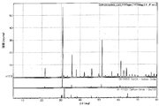
- FIG. 6 is a diagram showing a chart obtained by X-ray diffraction of Example 2.
- FIG. 6 is a diagram showing a chart obtained by X-ray diffraction in Example 3.
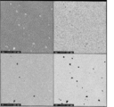
- FIG. It is a figure which shows the observation result by EPMA (electron beam microanalyzer) of Example 2.
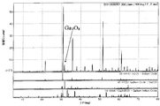
- FIG. It is a figure which shows the chart obtained by the X-ray diffraction of the comparative example 1.
- the oxide sintered body of the present invention contains indium (In), gallium (Ga), and an oxide of positive trivalent and / or positive tetravalent metal X. Further, the blending amount of X with respect to the total of In and Ga (hereinafter referred to as “X / (In + Ga)”) is 100 to 10,000 ppm (weight).
- the metal X is preferably one or more elements selected from Sn, Zr, Ti, Ge, and Hf.
- the metal X preferably contains at least Sn.
- the atomic ratio Ga / (In + Ga) is preferably 0.001 to 0.15. If Ga / (In + Ga) is less than 0.001, the change in lattice constant of the indium oxide crystal is small, and the effect of adding gallium may not appear. If it exceeds 0.15, InGaO 3 or the like may precipitate. is there. The more InGaO 3 or the like is deposited, the higher the electrical resistance of the target, and the more difficult the production by direct current sputtering with excellent productivity.
- the oxide sintered body of the present invention preferably consists essentially of oxides of indium, gallium and metal X. Preferably it does not contain silicon.
- “substantially” means that the effect as an oxide sintered body is due to the above, or 95 wt% to 100 wt% (preferably 98 wt% to 100 wt%) of the oxide sintered body.
- Means the following is an oxide of indium, gallium and metal X.
- the oxide sintered body of the present invention is substantially composed of oxides of indium, gallium, and metal X, and may contain other inevitable impurities as long as the effects of the present invention are not impaired.
- gallium and metal X are preferably dissolved and dispersed in an In 2 O 3 bixbite structure.
- the density of the oxide sintered body of the present invention is preferably 6.5 to 7.2 g / cm 3 . If the density is low, the surface of the sputtering target formed from the oxide sintered body may be blackened, causing abnormal discharge, and the sputtering rate may decrease. In order to increase the density of the sintered body, it is preferable to use a raw material having a particle diameter of 10 ⁇ m or less and to mix the raw materials uniformly. If the particle size is large, the reaction between the indium compound and the gallium compound may not proceed. Similarly, when not uniformly mixed, there is a possibility that unreacted or abnormally grown particles exist and the density does not increase.
- Ga is usually dispersed in indium oxide, but the diameter of the dispersed Ga aggregate is preferably 1 ⁇ m or less.
- the term “dispersion” used herein may mean that gallium ions are dissolved in the indium oxide crystal, or Ga compound particles may be finely dispersed in the indium oxide grains.
- Stable sputter discharge can be performed by finely dispersing Ga.
- the diameter of the Ga aggregate can be measured by EPMA (electron beam microanalyzer).
- the bulk resistance of the oxide sintered body of the present invention is preferably 10 m ⁇ cm or less.
- Ga is not completely dissolved and Ga 2 O 3 or the like is observed, abnormal discharge may be caused. More preferably, it is 5 m ⁇ cm or less. There is no particular lower limit, but it is not necessary to make it less than 1 m ⁇ cm.
- the oxide sintered body of the present invention contains 100 to 10,000 ppm of positive trivalent and / or positive tetravalent metal X with respect to In and Ga.
- a positive trivalent and / or positive tetravalent metal By including a positive trivalent and / or positive tetravalent metal, the resistance of the sintered body can be kept low.
- tin is preferable, and its concentration is preferably 100 ppm to 5000 ppm.
- the average particle diameter is measured by the method described in JIS R 1619.
- the indium compound, the gallium compound, and the metal X compound of the raw material powder to be used may be oxides or oxides after being fired (oxide precursors).
- Indium oxide precursors and metal X oxide precursors include indium or metal X sulfides, sulfates, nitrates, halides (chlorides, bromides, etc.), carbonates, organic acid salts (acetates, propions). Acid salt, naphthenate salt, etc.), alkoxide (methoxide, ethoxide, etc.), organometallic complex (acetylacetonate, etc.) and the like.
- nitrates, organic acid salts, alkoxides, or organometallic complexes are preferable in order to completely thermally decompose at low temperatures so that no impurities remain. It is optimal to use an oxide of each metal.
- the purity of each raw material is usually 99.9% by mass (3N) or more, preferably 99.99% by mass (4N) or more, more preferably 99.995% by mass or more, particularly preferably 99.999% by mass (5N ) That's it. If the purity of each raw material is 99.9% by mass (3N) or more, the semiconductor characteristics are not deteriorated by impurities such as metals other than the metal X that are positive tetravalent or higher, and impurities such as Fe, Ni, and Cu, and sufficient reliability is obtained. Can be retained. In particular, it is preferable that the content of Na, K, and Ca is 100 ppm or less because electrical resistance does not deteriorate over time when a thin film is produced.
- the mixing is preferably carried out by (i) solution method (coprecipitation method) or (ii) physical mixing method. More preferably, a physical mixing method is used for cost reduction.
- a physical mixing method is used for cost reduction.
- the raw material powder containing the above-mentioned indium compound, gallium compound and metal X compound is put in a mixer such as a ball mill, jet mill, pearl mill, or bead mill and mixed uniformly.
- the mixing time is preferably 1 to 200 hours. If it is less than 1 hour, the elements to be dispersed may be insufficiently homogenized, and if it exceeds 200 hours, it may take too much time and productivity may be deteriorated.
- a particularly preferred mixing time is 10 to 60 hours.
- the obtained raw material mixed powder preferably has an average particle size of 0.01 to 1.0 ⁇ m.
- the particle diameter is less than 0.01 ⁇ m, the powder is likely to aggregate, handling is poor, and a dense sintered body may not be obtained. On the other hand, if it exceeds 1.0 ⁇ m, a dense sintered body may not be obtained.
- a step of calcining the obtained mixture may be included.
- the mixture obtained in the above step is calcined.
- step (a) it is preferable to heat-treat the mixture obtained in step (a) at 200 to 1000 ° C. for 1 to 100 hours, more preferably 2 to 50 hours. If the heat treatment conditions are 200 ° C. or higher and 1 hour or longer, the raw material compound is sufficiently thermally decomposed. If the heat treatment conditions are 1000 ° C. or less and 100 hours or less, the particles are not coarsened.
- the mixture after calcining obtained here is pulverized before the subsequent molding step and sintering step.
- the mixture after calcination is suitably pulverized using a ball mill, roll mill, pearl mill, jet mill or the like.
- the average particle size of the mixture after calcining obtained after pulverization is, for example, 0.01 to 3.0 ⁇ m, preferably 0.1 to 2.0 ⁇ m. If the average particle size of the obtained mixture after calcining is 0.01 ⁇ m or more, it is preferable because a sufficient bulk specific gravity can be maintained and handling becomes easy.
- the average particle diameter of the mixture after calcining is 3.0 ⁇ m or less, it becomes easy to increase the density of the finally obtained sputtering target.
- the average particle diameter of the raw material powder can be measured by the method described in JIS R 1619.
- the mixed raw material powder can be molded by a known method such as pressure molding or cold isostatic pressing.
- a known molding method such as a cold press method or a hot press method can be used.
- the obtained mixed powder is filled in a mold and pressure-molded with a cold press machine.
- the pressure molding is performed, for example, at normal temperature (25 ° C.) at 100 to 100,000 kg / cm 2 .
- An oxide sintered body is manufactured by firing a compact of a raw material powder.
- the sintering temperature is 1200 to 1600 ° C, preferably 1250 to 1580 ° C, particularly preferably 1300 to 1550 ° C.
- gallium is easily dissolved in indium oxide, and the bulk resistance can be lowered. Moreover, by setting the sintering temperature to 1600 ° C. or less, transpiration of Ga and Sn can be suppressed.
- the sintering time is 2 to 96 hours, preferably 10 to 72 hours.
- the sintered density of the obtained oxide sintered body can be improved and the surface can be processed. Further, by setting the sintering time to 96 hours or less, the sintering can be performed in an appropriate time.
- Sintering is preferably performed in an oxygen gas atmosphere.
- an oxygen gas atmosphere By sintering in an oxygen gas atmosphere, the density of the obtained oxide sintered body can be increased, and abnormal discharge during sputtering of the oxide sintered body can be suppressed.
- the oxygen gas atmosphere is preferably an atmosphere having an oxygen concentration of, for example, 10 to 100 vol%. However, you may carry out in non-oxidizing atmosphere, for example, a vacuum or nitrogen atmosphere.
- sintering can be performed under atmospheric pressure or under pressure.
- the pressure is, for example, 9800 to 1000000 Pa, preferably 100000 to 500000 Pa.
- the oxide sintered body of the present invention can be manufactured by the method described above.
- the oxide sintered body of the present invention can be used as a sputtering target. Since the oxide sintered body of the present invention has high conductivity, a DC sputtering method having a high film formation rate can be applied when a sputtering target is used.
- the sputtering target of the present invention can be applied to any sputtering method such as an RF sputtering method, an AC sputtering method, and a pulsed DC sputtering method in addition to the DC sputtering method, and can perform sputtering without abnormal discharge.
- a sputtering method such as an RF sputtering method, an AC sputtering method, and a pulsed DC sputtering method in addition to the DC sputtering method, and can perform sputtering without abnormal discharge.
- the oxide thin film can be produced using the above oxide sintered body by vapor deposition, sputtering, ion plating, pulse laser vapor deposition, or the like.
- sputtering methods include RF magnetron sputtering, DC magnetron sputtering, AC magnetron sputtering, and pulsed DC magnetron sputtering.
- the sputtering gas a mixed gas of an inert gas such as argon and a reactive gas such as oxygen, water, or hydrogen can be used.
- the partial pressure of the reactive gas during sputtering varies depending on the discharge method and power, but is preferably about 0.1% or more and 20% or less. If it is less than 0.1%, the transparent amorphous film immediately after film formation has conductivity, and it may be difficult to use it as an oxide semiconductor. On the other hand, if it exceeds 20%, the transparent amorphous film becomes an insulator, and it may be difficult to use it as an oxide semiconductor. Preferably, it is 1 to 10%.
- the oxide thin film of the present invention is formed using the above-described sputtering target of the present invention.
- the oxide thin film of the present invention contains indium (In), gallium (Ga), and positive trivalent and / or positive tetravalent metal X oxide, and X / (In + Ga) is 100 to 10000 ppm.
- the atomic ratio Ga / (In + Ga) is preferably 0.005 to 0.08.
- the oxide thin film consists essentially of oxides of indium, gallium and metal X and does not contain silicon.
- the metal X is preferably at least one selected from Sn, Zr, Ti, Ge, and Hf.
- the oxide thin film of the present invention has an In 2 O 3 bixbite structure, gallium is dissolved in indium oxide, and an atomic ratio Ga / (In + Ga) is 0.001 to 0.15. is there.
- Gallium has the effect of reducing the lattice constant of indium oxide, and thus has the effect of increasing the mobility.
- the bonding strength with oxygen is strong, and there is an effect of reducing the amount of oxygen deficiency in the polycrystalline indium oxide thin film.
- Gallium has a region that completely dissolves with indium oxide, and is completely integrated with crystallized indium oxide, thereby reducing the lattice constant.
- the precipitated gallium oxide may cause scattering of electrons or may inhibit crystallization of indium oxide.
- the additive element X has an effect of increasing the heat conduction of the target. Therefore, cracks such as cracks can be prevented when bonding a large sintered body excellent in productivity.
- the ratio of Ga / (Ga + In) exceeds 0.10, the heat conduction of the target is extremely lowered, but this can be prevented by adding X.
- the oxide thin film of the present invention is usually composed of a single phase having a bixbite structure, and the lower limit of the lattice constant of the bixbite structure is not particularly limited, but is preferably not less than 10.01 ⁇ and less than 10.118 ⁇ .
- a low lattice constant means that the crystal lattice is reduced and the distance between metals is small. By reducing the distance between the metals, the speed of movement of electrons moving on the metal trajectory increases, and the mobility of the obtained thin film transistor increases. If the lattice constant is too large, it becomes equal to the crystal lattice of indium oxide itself, and the mobility is not improved.
- the diameter of the dispersed Ga aggregate is preferably less than 1 ⁇ m.
- the oxide thin film of the present invention can be used as an active layer of an oxide semiconductor element.
- the oxide semiconductor element include a thin film transistor, a power transistor, and a phase change memory.
- the oxide thin film of the present invention can be preferably used for a thin film transistor. In particular, it can be used as a channel layer.
- the oxide thin film can be used as it is or after heat treatment.
- the thin film transistor may be a channel etch type. Since the thin film of the present invention is crystalline and durable, a photolithographic process in which a metal thin film such as Al is etched to form a source / drain electrode and a channel portion in the manufacture of a thin film transistor using the thin film of the present invention is also possible. It becomes.
- the thin film transistor may be an etch stopper type.
- the etch stopper can protect the channel portion formed of the semiconductor layer, and a large amount of oxygen can be taken into the semiconductor film at the time of film formation. There is no need to supply oxygen.
- the source / drain electrodes and channel part are formed by etching a metal thin film such as Al, and at the same time, the semiconductor layer can be etched to shorten the photolithography process. Become.
- the thin film transistor may be a top contact type or a bottom contact type.
- contact resistance tends to occur at the interface with the oxide semiconductor due to the influence of moisture and oxide film adhering to the surface of the source / drain electrode. Therefore, by performing reverse sputtering or removing these by vacuum heating before the oxide semiconductor sputtering film formation, the contact resistance is reduced and a good transistor can be easily obtained.
- a method of manufacturing a thin film transistor includes a step of forming an oxide thin film using the sputtering target of the present invention, a step of heat-treating the oxide thin film in an oxygen atmosphere, and an oxide insulator layer on the heat-treated oxide thin film. Forming. Crystallize by heat treatment.
- an oxide insulator layer is preferably formed on the heat-treated oxide thin film in order to prevent deterioration of semiconductor characteristics over time.
- the oxide thin film is formed in a deposition gas having an oxygen content of 10% by volume or more.
- a deposition gas having an oxygen content of 10% by volume or more for example, a mixed gas of argon and oxygen or a mixed gas of argon and water vapor is used.
- the oxidation reaction proceeds with oxygen gas alone, but oxygen deficiency tends to remain. If there are many oxygen vacancies, it may act as a trap or donor near the conductor, leading to a decrease in the On / Off ratio and a decrease in the S value. Also, how the plasma spreads is important so that OH. In particular, in the case of a large substrate, uniformity can be ensured by slowing the swing speed of the magnet at the end.
- the concentration of water introduced during sputtering varies depending on the sputtering apparatus and manufacturing conditions, and is not simple, but depends on how the plasma spreads, the difference in the discharge method, the deposition rate, the substrate / target distance, and the like.
- hydrogen and oxygen may be introduced simultaneously instead of water.
- oxygen needs to be introduced at a ratio of 1: 2 or more with respect to hydrogen. Also in this case, it is important to control the concentration of OH.
- a lamp annealing device In the crystallization process of the oxide thin film, a lamp annealing device, a laser annealing device, a thermal plasma device, a hot air heating device, a contact heating device, or the like can be used in the presence or absence of oxygen.
- the temperature rising rate is usually 40 ° C./min or more, preferably 70 ° C./min or more, more preferably 80 ° C./min, and further preferably 100 ° C./min or more.
- the heating rate there is no upper limit to the heating rate, and in the case of heating by laser heating or thermal plasma, the temperature can be instantaneously increased to a desired heat treatment temperature.
- the cooling rate is also high, if the substrate speed is too high, the substrate may be cracked, or internal stress may remain in the thin film, which may lower the electrical characteristics. When the cooling rate is too low, the crystal may grow abnormally due to the annealing effect, and it is preferable to set the cooling rate similarly to the heating rate.
- the cooling rate is usually 5 to 300 ° C./min, more preferably 10 to 200 ° C./min, and still more preferably 20 to 100 ° C./min.
- the heat treatment of the oxide thin film is preferably performed at 250 to 500 ° C. for 0.5 to 1200 minutes. If it is less than 250 ° C., crystallization may not be achieved, and if it exceeds 500 ° C., the substrate and the semiconductor film may be damaged. In addition, if it is less than 0.5 minutes, the heat treatment time is too short, and crystallization may not be achieved, and if it is 1200 minutes, it may take too much time.
- Examples 1-8 The following oxide powder was used as the raw material powder.
- the average particle diameter was measured by a laser diffraction particle size distribution analyzer SALD-300V (manufactured by Shimadzu Corporation), and the specific surface area was measured by the BET method.
- B Gallium oxide powder: specific surface area 6 m 2 / g, average particle size 1.5 ⁇ m
- C Tin oxide powder: specific surface area 6 m 2 / g, average particle size 1.5 ⁇ m
- D Oxidized zirconia powder: specific surface area 6 m 2 / g, average particle size 1.5 ⁇ m
- Germanium oxide powder specific surface area 6 m 2 / g, average particle size 1.5 ⁇ m
- the specific surface area of the entire raw material mixed powder composed of (a) and (b) was 6.0 m 2 / g.
- the above powder was weighed so as to have a Ga / (In + Ga) ratio and X / (In + Ga) shown in Table 1, and mixed and ground using a wet medium stirring mill.
- a grinding medium 1 mm ⁇ zirconia beads were used.
- the specific surface area was increased by 2 m 2 / g from the specific surface area of the raw material mixed powder while confirming the specific surface area of the mixed powder.
- the mixed powder obtained by drying with a spray dryer was filled in a mold (350 mm ⁇ 20 mm thick) and pressure-molded with a cold press machine. After the molding, the sintered body was manufactured by sintering for 20 hours at a temperature shown in Table 1 in an oxygen atmosphere while circulating oxygen.
- the density of the manufactured sintered body was calculated from the weight and outer dimensions of the sintered body cut into a size of 200 mm ⁇ ⁇ 10 mm.
- the sintered compact for sputtering targets with a high density of a sintered compact was able to be obtained, without performing a calcination process.
- the bulk resistance (conductivity) (m ⁇ cm) of the sintered body was measured by a four-probe method using a resistivity meter (manufactured by Mitsubishi Oil Chemical Co., Ltd., Loresta).
- the elemental composition ratio (atomic ratio) of the sintered body was measured by an induction plasma emission analyzer (ICP-AES).
- the atomic ratio of the sintered body corresponded to the atomic ratio of the raw material. The results are shown in Table 1.
- FIG. 1 and 2 show X-ray charts of Examples 2 and 3.
- FIG. 3 shows the observation results of EPMA.
- FIG. 3 shows that Ga is uniformly dissolved in In 2 O 3 .
- Ga 2 O 3 is also observed in part, but the diameter is 1 ⁇ m or less.
- the obtained sintered body was bonded to a backing plate to obtain a 200 mm ⁇ sputtering target.
- a copper backing plate was placed on a hot plate, a 0.2 mm indium wire was placed thereon, and a sintered body was placed thereon. Thereafter, the hot plate was heated to 250 ° C., and indium was fused to obtain a sputtering target.
- a metal mask was placed to form a channel portion of L: 200 ⁇ m and W: 1000 ⁇ m, and source / drain electrodes were formed by vapor deposition of gold.
- the device was annealed in air in a heating furnace heated to 300 ° C. for 1 hour, and the XRD (X-ray diffraction) of the channel portion was measured.
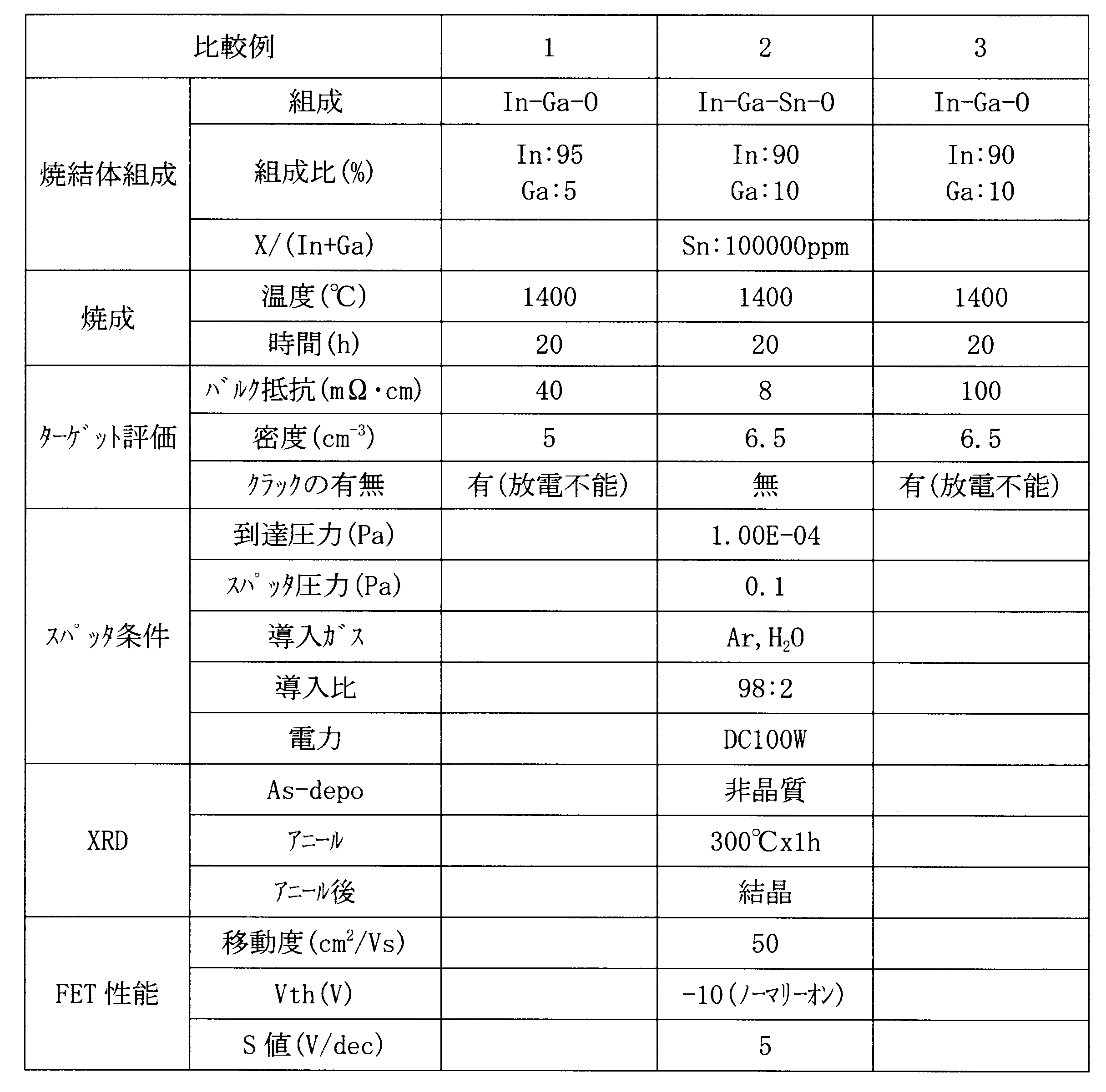
- Comparative Examples 1 to 3 A sintered body was produced and evaluated in the same manner as in Example 1 except that the raw material powders were mixed and sintered at the ratio shown in Table 2. The results are shown in Table 2.
- FIG. 4 shows a chart obtained by X-ray diffraction of Comparative Example 1. In addition to In 2 O 3 bixbite, a Ga 2 O 3 structure was also confirmed in the X-ray diffraction chart.
- the targets of Comparative Examples 1 and 3 cracked when bonded. This is presumably because the heat conduction was inferior due to the presence of two types of crystals.
- a transistor was fabricated and evaluated in the same manner as in Example 8 using the target of Comparative Example 2 in which no cracks occurred. As a result, the semiconductor of Comparative Example 2 had high conductivity due to the large amount of tin added, and the threshold voltage was -10 V, which was inferior to other semiconductors.
- the oxide sintered body of the present invention can be used as a sputtering target.
- a thin film formed using the sputtering target of the present invention can be used for a thin film transistor.
Landscapes
- Chemical & Material Sciences (AREA)
- Engineering & Computer Science (AREA)
- Ceramic Engineering (AREA)
- Materials Engineering (AREA)
- Organic Chemistry (AREA)
- Manufacturing & Machinery (AREA)
- Structural Engineering (AREA)
- Mechanical Engineering (AREA)
- Chemical Kinetics & Catalysis (AREA)
- Metallurgy (AREA)
- Inorganic Chemistry (AREA)
- Dispersion Chemistry (AREA)
- Microelectronics & Electronic Packaging (AREA)
- Physical Vapour Deposition (AREA)
- Compositions Of Oxide Ceramics (AREA)
- Thin Film Transistor (AREA)
Abstract
Description
1.インジウム(In)、ガリウム(Ga)及び正三価及び/又は正四価の金属Xの酸化物を含有し、InとGaの合計に対する金属Xの配合量が100~10000ppm(重量)であることを特徴とする酸化物焼結体。
2.金属Xが、Sn,Zr,Ti,Ge,Hfから選ばれる1種以上であることを特徴とする1に記載の酸化物焼結体。
3.前記金属Xが少なくともSnを含有することを特徴とする1又は2に記載の酸化物焼結体。
4.原子比Ga/(Ga+In)が、0.005~0.15であることを特徴とする1~3のいずれかに記載の酸化物焼結体。
5.バルク抵抗が10mΩcm以下であることを特徴とする1~4のいずれかに記載の酸化物焼結体。
6.分散しているガリウムの粒径が1μm以下であることを特徴とする1~5のいずれかに記載の酸化物焼結体。
7.In2O3のビックスバイト構造に、ガリウムと金属Xが固溶分散していることを特徴とする1~6のいずれかに記載の酸化物焼結体。
8.平均粒径が2μm未満のインジウム化合物粉末と、平均粒径が2μm未満のガリウム化合物粉末と、平均粒径が2μm未満の金属Xの化合物の粉末を、ガリウムとインジウムの原子比Ga/(In+Ga)=0.001~0.10、及びInとGaの合計に対する金属Xの配合量が100~10000ppmとなるように混合する工程、混合物を成形して成形体を調製する工程、及び前記成形体を1200℃~1600℃で2~96時間焼成する工程を含むことを特徴とする1~7のいずれかに記載の酸化物焼結体の製造方法。
9.焼成を酸素雰囲気中又は加圧下で行うことを特徴とする8に記載の酸化物焼結体の製造方法。
10.1~7のいずれかに記載の酸化物焼結体からなることを特徴とするスパッタリングターゲット。
11.10に記載のスパッタリングターゲットを用いて成膜されたことを特徴とする酸化物薄膜。
12.インジウム(In)、ガリウム(Ga)及び正三価及び/又は正四価の金属Xの酸化物を含有し、InとGaの合計に対する金属Xの配合量が100~10000ppm(重量)であることを特徴とする酸化物薄膜。
13.活性層が11又は12に記載の酸化物薄膜からなることを特徴とする酸化物半導体素子。
金属Xは、好ましくはSn,Zr,Ti,Ge,Hfから選ばれる1種以上の元素である。金属Xは好ましくは少なくともSnを含有する。
Ga/(In+Ga)が0.001未満では、酸化インジウム結晶の格子定数の変化が小さくなり、ガリウムを添加する効果が現れない場合があり、0.15超では、InGaO3等が析出する場合がある。InGaO3等が析出するほど、ターゲットの電気抵抗が高くなり、生産性に優れた直流スパッタによる生産が行いにくくなる。
好ましくはGa/(In+Ga)=0.005~0.15であり、より好ましくはGa/(In+Ga)=0.01~0.12であり、さらに好ましくはGa/(In+Ga)=0.03~0.10である。
本発明において「実質的」とは、酸化物焼結体としての効果が上記に起因すること、又は酸化物焼結体の95重量%以上100重量%以下(好ましくは98重量%以上100重量%以下)がインジウム、ガリウム及び金属Xの酸化物であることを意味する。
上記のように本発明の酸化物焼結体は、実質的にインジウム、ガリウム及び金属Xの酸化物からなり、本発明の効果を損なわない範囲で他に不可避不純物を含んでいてもよい。
焼結体の密度を上げるためには、原料の粒子径が10μm以下のものを使用し、原料を均質に混合すると好ましい。粒子径が大きいとインジウム化合物とガリウム化合物の反応が進まない恐れがある。均質に混合されない場合も同様に、未反応や、異常粒成長した粒子が存在し密度が上がらない恐れがある。
金属Xとインジウム金属の原子比は好ましくはX/(In+Ga)=200~5000ppmである。より好ましくはX/(In+Ga)=300~3000ppm、さらに好ましくはX/(In+Ga)=500~1000ppmである。
(a)平均粒径が2μm未満のIn化合物粉末と、平均粒径が2μm未満のGa化合物粉末と、平均粒径が2μm未満の金属Xの化合物粉末を、ガリウムとインジウムの原子比Ga/(In+Ga)=0.001~0.10、Xとインジウム・ガリウムとの原子比X/(In+Ga)=100~10000ppmで混合して混合物を調製する工程;
(b)前記混合物を成形して成形体を調製する工程;及び
(c)前記成形体を1200℃~1600℃で2~96時間焼成する工程を含む。
尚、平均粒径はJIS R 1619に記載の方法により測定する。
物理混合法では、上記のインジウム化合物、ガリウム化合物及び金属Xの化合物を含む原料粉体を、ボールミル、ジェットミル、パールミル、ビーズミル等の混合器に入れ、均一に混合する。
加圧成形は、コールドプレス(Cold Press)法やホットプレス(Hot Press)法等、公知の成形方法を用いることができる。例えば、得られた混合粉を金型に充填し、コールドプレス機にて加圧成形する。加圧成形は、例えば常温(25℃)下、100~100000kg/cm2で行われる。
焼結温度は1200~1600℃であり、好ましくは1250~1580℃であり、特に好ましくは1300~1550℃である。
焼結時間は2~96時間であり、好ましくは10~72時間である。
また、本発明の酸化物薄膜は、インジウム(In)、ガリウム(Ga)及び正三価及び/又は正四価の金属Xの酸化物を含有し、X/(In+Ga)が100~10000ppmである。原子比Ga/(In+Ga)は、好ましくは0.005~0.08である。好ましくは、酸化物薄膜は実質的にインジウム、ガリウム及び金属Xの酸化物のみからなり、珪素を含まない。
金属Xは、好ましくはSn,Zr,Ti,Ge,Hfから選ばれる1種以上である。また好ましくは、本発明の酸化物薄膜はIn2O3のビックスバイト構造を有し、ガリウムが酸化インジウムに固溶していて、原子比Ga/(In+Ga)が0.001~0.15である。
また、添加元素Xはターゲットの熱伝導を高める効果がある。従って、生産性に優れた大型の焼結体をボンディングする際に、クラック等の割れを防止することができる。
Ga/(Ga+In)の比が0.10を超えると、ターゲットの熱伝導は極端に低下するが、Xを添加することでこれを防止できる。
本発明の酸化物薄膜は好ましくは、分散しているGaの集合体の直径が1μm未満である。
本発明の酸化物薄膜は好ましくは薄膜トランジスタに使用できる。特にチャネル層として使用できる。酸化物薄膜はそのまま又は熱処理して使用できる。
成膜ガス中の酸素濃度を10体積%以上、あるいは水蒸気の濃度を1体積%以上とすることで、後に続く結晶化を安定化することができる。
In2O3-x+2xOH・→In2O3+xH2O
また、スパッタ中にOH・が基板全体に均一に行き渡るように、プラズマの広がり方も重要である。特に大型基板の場合、マグネットの揺動速度を端部で遅くすることで、均一性を確保することが可能となる。スパッタ中に導入する水の濃度は、スパッタ装置や製造条件により異なるため、単純ではないが、プラズマの広がり方、放電方式の違い、成膜速度、基板・ターゲット距離などに依存する。
冷却速度も高い方が好ましいが、基板速度が大きすぎる場合は基板が割れたり、薄膜に内部応力が残るために電気特性が下がる恐れがある。冷却速度が低すぎる場合は、アニール効果により、結晶が異常に成長する可能性があり、加熱速度と同様に冷却速度を設定することが好ましい。冷却速度は、通常、5~300℃/分、より好ましくは10~200℃/分、さらに好ましくは、20~100℃/分である。
原料粉体として、下記の酸化物粉末を使用した。尚、平均粒径はレーザ回折式粒度分布測定装置SALD-300V(島津製作所製)で、比表面積はBET法で測定した。
(a)酸化インジウム粉:比表面積6m2/g、平均粒径1.2μm
(b)酸化ガリウム粉:比表面積6m2/g、平均粒径1.5μm
(c)酸化錫粉:比表面積6m2/g、平均粒径1.5μm
(d)酸化ジルコニア粉:比表面積6m2/g、平均粒径1.5μm
(e)酸化チタン粉:比表面積6m2/g、平均粒径1.5μm
(f)酸化ゲルマニウム粉:比表面積6m2/g、平均粒径1.5μm
(a)及び(b)からなる原料混合粉体全体の比表面積は6.0m2/gであった。
また、この焼結体のバルク抵抗(導電性)(mΩcm)を、抵抗率計(三菱油化製、ロレスタ)を使用し四探針法により測定した。
この焼結体の元素組成比(原子比)は、誘導プラズマ発光分析装置(ICP-AES)により測定した。焼結体の原子比は原料の原子比と対応していた。結果を表1に示す。
チャートを分析した結果、実施例2,3の焼結体中には、In2O3のビックスバイト構造が観察された。また、Ga2O3構造はほとんど認めることができなかった。
また、実施例2で作製した焼結体をEPMAで観察した結果、In2O3中にGaが固溶しており、Gaの直径は1μm以下であることを確認した。
図3にEPMAの観察結果を示す。図3より、GaはIn2O3に均一固溶していることが分かる。図3の右上の像において、一部にGa2O3も観察されるが、直径は1μm以下である。
当該素子を、空気中、300℃に加熱した加熱炉内で1時間アニールし、チャネル部分のXRD(X線回折)を測定したところ全て結晶化していた。

表2に示す比で原料粉末を混合し、焼結した他は、実施例1と同様に焼結体を製造し、評価した。結果を表2に示す。
図4には比較例1のX線回折により得られたチャートを示す。X線回折チャートにはIn2O3のビックスバイトの他、Ga2O3構造も確認された。
クラックの入らなかった比較例2のターゲットを用いて、実施例8と同様にしてトランジスタを作製し、評価した。その結果、比較例2の半導体は錫の添加量が多いため導電性が高く、閾値電圧が-10Vと他の半導体に比べて劣っていた。
この明細書に記載の文献の内容を全てここに援用する。
Claims (13)
- インジウム(In)、ガリウム(Ga)及び正三価及び/又は正四価の金属Xの酸化物を含有し、InとGaの合計に対する金属Xの配合量が100~10000ppm(重量)であることを特徴とする酸化物焼結体。
- 金属Xが、Sn,Zr,Ti,Ge,Hfから選ばれる1種以上であることを特徴とする請求項1に記載の酸化物焼結体。
- 前記金属Xが少なくともSnを含有することを特徴とする請求項1又は2に記載の酸化物焼結体。
- 原子比Ga/(Ga+In)が、0.005~0.15であることを特徴とする請求項1~3のいずれかに記載の酸化物焼結体。
- バルク抵抗が10mΩcm以下であることを特徴とする請求項1~4のいずれかに記載の酸化物焼結体。
- 分散しているガリウムの粒径が1μm以下であることを特徴とする請求項1~5のいずれかに記載の酸化物焼結体。
- In2O3のビックスバイト構造に、ガリウムと金属Xが固溶分散していることを特徴とする請求項1~6のいずれかに記載の酸化物焼結体。
- 平均粒径が2μm未満のインジウム化合物粉末と、平均粒径が2μm未満のガリウム化合物粉末と、平均粒径が2μm未満の金属Xの化合物の粉末を、ガリウムとインジウムの原子比Ga/(In+Ga)=0.001~0.10、及びInとGaの合計に対する金属Xの配合量が100~10000ppmとなるように混合する工程、混合物を成形して成形体を調製する工程、及び前記成形体を1200℃~1600℃で2~96時間焼成する工程を含むことを特徴とする請求項1~7のいずれかに記載の酸化物焼結体の製造方法。
- 焼成を酸素雰囲気中又は加圧下で行うことを特徴とする請求項8に記載の酸化物焼結体の製造方法。
- 請求項1~7のいずれかに記載の酸化物焼結体からなることを特徴とするスパッタリングターゲット。
- 請求項10に記載のスパッタリングターゲットを用いて成膜されたことを特徴とする酸化物薄膜。
- インジウム(In)、ガリウム(Ga)及び正三価及び/又は正四価の金属Xの酸化物を含有し、InとGaの合計に対する金属Xの配合量が100~10000ppm(重量)であることを特徴とする酸化物薄膜。
- 活性層が請求項11又は12に記載の酸化物薄膜からなることを特徴とする酸化物半導体素子。
Priority Applications (5)
| Application Number | Priority Date | Filing Date | Title |
|---|---|---|---|
| US13/700,789 US20130140502A1 (en) | 2010-02-06 | 2011-06-01 | Sputtering target |
| CN201180027030.6A CN102918004B (zh) | 2010-06-02 | 2011-06-01 | 溅射靶 |
| KR1020187005081A KR101960233B1 (ko) | 2010-06-02 | 2011-06-01 | 스퍼터링 타겟 |
| KR1020127031466A KR102012853B1 (ko) | 2010-06-02 | 2011-06-01 | 스퍼터링 타겟 |
| JP2012518254A JP5763064B2 (ja) | 2010-06-02 | 2011-06-01 | スパッタリングターゲット |
Applications Claiming Priority (2)
| Application Number | Priority Date | Filing Date | Title |
|---|---|---|---|
| JP2010-126497 | 2010-02-06 | ||
| JP2010126497 | 2010-06-02 |
Publications (1)
| Publication Number | Publication Date |
|---|---|
| WO2011152048A1 true WO2011152048A1 (ja) | 2011-12-08 |
Family
ID=45066439
Family Applications (1)
| Application Number | Title | Priority Date | Filing Date |
|---|---|---|---|
| PCT/JP2011/003087 Ceased WO2011152048A1 (ja) | 2010-02-06 | 2011-06-01 | スパッタリングターゲット |
Country Status (6)
| Country | Link |
|---|---|
| US (1) | US20130140502A1 (ja) |
| JP (1) | JP5763064B2 (ja) |
| KR (2) | KR101960233B1 (ja) |
| CN (1) | CN102918004B (ja) |
| TW (1) | TWI527916B (ja) |
| WO (1) | WO2011152048A1 (ja) |
Cited By (3)
| Publication number | Priority date | Publication date | Assignee | Title |
|---|---|---|---|---|
| JPWO2013103034A1 (ja) * | 2012-01-06 | 2015-05-11 | Jx日鉱日石金属株式会社 | 水酸化ガリウムの製造方法、酸化ガリウム粉末の製造方法、酸化ガリウム粉末、該酸化ガリウムの焼結体及び該焼結体からなるスパッタリングターゲット |
| CN104798205A (zh) * | 2012-11-22 | 2015-07-22 | 住友金属矿山株式会社 | 氧化物半导体薄膜及其制造方法以及薄膜晶体管 |
| US10128108B2 (en) | 2014-11-25 | 2018-11-13 | Sumitomo Metal Mining Co., Ltd. | Oxide sintered body, sputtering target, and oxide semiconductor thin film obtained using sputtering target |
Families Citing this family (9)
| Publication number | Priority date | Publication date | Assignee | Title |
|---|---|---|---|---|
| JP6424892B2 (ja) * | 2014-06-26 | 2018-11-21 | 住友金属鉱山株式会社 | 酸化物焼結体、スパッタリング用ターゲット、及びそれを用いて得られる酸化物半導体薄膜 |
| EP3196892B1 (en) * | 2014-08-28 | 2020-02-26 | Fujitsu Ltd. | Solid electrolyte, method for manufacturing same, all-solid-state secondary cell, and method for manufacturing same |
| JP6418060B2 (ja) * | 2015-05-13 | 2018-11-07 | 住友金属鉱山株式会社 | 金属吸収層の製造方法と積層体フィルムの製造方法 |
| CN109641757B (zh) * | 2016-08-31 | 2022-02-25 | 出光兴产株式会社 | 石榴石型化合物、含有该化合物的烧结体以及溅射靶 |
| US20250326693A1 (en) * | 2021-03-12 | 2025-10-23 | Technische Universität Darmstadt | Method and device for producing ceramics and ceramic product |
| CN117083173A (zh) * | 2021-03-12 | 2023-11-17 | 达姆施塔特工业大学 | 用于生产陶瓷的方法和装置以及陶瓷产品 |
| CN113651598B (zh) * | 2021-08-11 | 2022-06-21 | 芜湖映日科技股份有限公司 | 一种izo掺杂靶材及其制备方法 |
| CN114481028B (zh) * | 2022-01-18 | 2024-03-29 | 浙江爱旭太阳能科技有限公司 | 一种异质结电池的tco薄膜及其制作方法 |
| CN119306475B (zh) * | 2024-09-04 | 2026-04-17 | 中山智隆新材料科技有限公司 | 一种氧化铟镓钛靶材及其制备方法和应用 |
Citations (4)
| Publication number | Priority date | Publication date | Assignee | Title |
|---|---|---|---|---|
| WO2000068456A1 (fr) * | 1999-05-10 | 2000-11-16 | Japan Energy Corporation | Cible de pulverisation cathodique et procede de production de celle-ci |
| WO2009008297A1 (ja) * | 2007-07-06 | 2009-01-15 | Sumitomo Metal Mining Co., Ltd. | 酸化物焼結体とその製造方法、ターゲット、及びそれを用いて得られる透明導電膜ならびに透明導電性基材 |
| WO2009148154A1 (ja) * | 2008-06-06 | 2009-12-10 | 出光興産株式会社 | 酸化物薄膜用スパッタリングターゲットおよびその製造法 |
| WO2010032422A1 (ja) * | 2008-09-19 | 2010-03-25 | 出光興産株式会社 | 酸化物焼結体及びスパッタリングターゲット |
Family Cites Families (1)
| Publication number | Priority date | Publication date | Assignee | Title |
|---|---|---|---|---|
| JP2004149883A (ja) | 2002-10-31 | 2004-05-27 | Mitsui Mining & Smelting Co Ltd | 高抵抗透明導電膜用スパッタリングターゲット及び高抵抗透明導電膜の製造方法 |
-
2011
- 2011-06-01 JP JP2012518254A patent/JP5763064B2/ja active Active
- 2011-06-01 WO PCT/JP2011/003087 patent/WO2011152048A1/ja not_active Ceased
- 2011-06-01 KR KR1020187005081A patent/KR101960233B1/ko active Active
- 2011-06-01 CN CN201180027030.6A patent/CN102918004B/zh active Active
- 2011-06-01 US US13/700,789 patent/US20130140502A1/en not_active Abandoned
- 2011-06-01 KR KR1020127031466A patent/KR102012853B1/ko active Active
- 2011-06-02 TW TW100119461A patent/TWI527916B/zh active
Patent Citations (4)
| Publication number | Priority date | Publication date | Assignee | Title |
|---|---|---|---|---|
| WO2000068456A1 (fr) * | 1999-05-10 | 2000-11-16 | Japan Energy Corporation | Cible de pulverisation cathodique et procede de production de celle-ci |
| WO2009008297A1 (ja) * | 2007-07-06 | 2009-01-15 | Sumitomo Metal Mining Co., Ltd. | 酸化物焼結体とその製造方法、ターゲット、及びそれを用いて得られる透明導電膜ならびに透明導電性基材 |
| WO2009148154A1 (ja) * | 2008-06-06 | 2009-12-10 | 出光興産株式会社 | 酸化物薄膜用スパッタリングターゲットおよびその製造法 |
| WO2010032422A1 (ja) * | 2008-09-19 | 2010-03-25 | 出光興産株式会社 | 酸化物焼結体及びスパッタリングターゲット |
Cited By (3)
| Publication number | Priority date | Publication date | Assignee | Title |
|---|---|---|---|---|
| JPWO2013103034A1 (ja) * | 2012-01-06 | 2015-05-11 | Jx日鉱日石金属株式会社 | 水酸化ガリウムの製造方法、酸化ガリウム粉末の製造方法、酸化ガリウム粉末、該酸化ガリウムの焼結体及び該焼結体からなるスパッタリングターゲット |
| CN104798205A (zh) * | 2012-11-22 | 2015-07-22 | 住友金属矿山株式会社 | 氧化物半导体薄膜及其制造方法以及薄膜晶体管 |
| US10128108B2 (en) | 2014-11-25 | 2018-11-13 | Sumitomo Metal Mining Co., Ltd. | Oxide sintered body, sputtering target, and oxide semiconductor thin film obtained using sputtering target |
Also Published As
| Publication number | Publication date |
|---|---|
| CN102918004A (zh) | 2013-02-06 |
| CN102918004B (zh) | 2016-03-30 |
| KR20180023033A (ko) | 2018-03-06 |
| JP5763064B2 (ja) | 2015-08-12 |
| US20130140502A1 (en) | 2013-06-06 |
| KR20130085947A (ko) | 2013-07-30 |
| TWI527916B (zh) | 2016-04-01 |
| JPWO2011152048A1 (ja) | 2013-07-25 |
| TW201144458A (en) | 2011-12-16 |
| KR102012853B1 (ko) | 2019-08-21 |
| KR101960233B1 (ko) | 2019-03-19 |
Similar Documents
| Publication | Publication Date | Title |
|---|---|---|
| JP5763064B2 (ja) | スパッタリングターゲット | |
| JP5759530B2 (ja) | 酸化物焼結体及びスパッタリングターゲット | |
| TWI595668B (zh) | 氧化物半導體薄膜及薄膜電晶體 | |
| CN106103380A (zh) | 氧化物烧结体、溅射用靶及使用该靶得到的氧化物半导体薄膜 | |
| JP6387823B2 (ja) | 酸化物焼結体、スパッタリング用ターゲット、及びそれを用いて得られる酸化物半導体薄膜 | |
| TWI591195B (zh) | 氧化物燒結體、濺鍍用靶、及使用其而獲得之氧化物半導體薄膜 | |
| TWI547573B (zh) | 氧化物燒結體、濺鍍用靶、及使用其而獲得之氧化物半導體薄膜 | |
| TWI622568B (zh) | 氧化物燒結體及濺鍍用靶 | |
| TW201638013A (zh) | 氧化物燒結體、濺鍍用靶、及使用其而得之氧化物半導體薄膜 | |
| TW202347771A (zh) | 半導體膜及半導體膜之製造方法 | |
| JP2017168572A (ja) | 酸化物半導体薄膜、酸化物焼結体、薄膜トランジスタ及び表示装置 |
Legal Events
| Date | Code | Title | Description |
|---|---|---|---|
| WWE | Wipo information: entry into national phase |
Ref document number: 201180027030.6 Country of ref document: CN |
|
| 121 | Ep: the epo has been informed by wipo that ep was designated in this application |
Ref document number: 11789461 Country of ref document: EP Kind code of ref document: A1 |
|
| WWE | Wipo information: entry into national phase |
Ref document number: 2012518254 Country of ref document: JP |
|
| ENP | Entry into the national phase |
Ref document number: 20127031466 Country of ref document: KR Kind code of ref document: A |
|
| NENP | Non-entry into the national phase |
Ref country code: DE |
|
| WWE | Wipo information: entry into national phase |
Ref document number: 13700789 Country of ref document: US |
|
| 122 | Ep: pct application non-entry in european phase |
Ref document number: 11789461 Country of ref document: EP Kind code of ref document: A1 |