WO2011149044A1 - 電気二重層キャパシタ - Google Patents
電気二重層キャパシタ Download PDFInfo
- Publication number
- WO2011149044A1 WO2011149044A1 PCT/JP2011/062183 JP2011062183W WO2011149044A1 WO 2011149044 A1 WO2011149044 A1 WO 2011149044A1 JP 2011062183 W JP2011062183 W JP 2011062183W WO 2011149044 A1 WO2011149044 A1 WO 2011149044A1
- Authority
- WO
- WIPO (PCT)
- Prior art keywords
- electrode
- layer capacitor
- electric double
- double layer
- polarizable
- Prior art date
- Legal status (The legal status is an assumption and is not a legal conclusion. Google has not performed a legal analysis and makes no representation as to the accuracy of the status listed.)
- Ceased
Links
Images


Classifications
-
- H—ELECTRICITY
- H01—ELECTRIC ELEMENTS
- H01G—CAPACITORS; CAPACITORS, RECTIFIERS, DETECTORS, SWITCHING DEVICES, LIGHT-SENSITIVE OR TEMPERATURE-SENSITIVE DEVICES OF THE ELECTROLYTIC TYPE
- H01G11/00—Hybrid capacitors, i.e. capacitors having different positive and negative electrodes; Electric double-layer [EDL] capacitors; Processes for the manufacture thereof or of parts thereof
- H01G11/04—Hybrid capacitors
-
- H—ELECTRICITY
- H01—ELECTRIC ELEMENTS
- H01G—CAPACITORS; CAPACITORS, RECTIFIERS, DETECTORS, SWITCHING DEVICES, LIGHT-SENSITIVE OR TEMPERATURE-SENSITIVE DEVICES OF THE ELECTROLYTIC TYPE
- H01G11/00—Hybrid capacitors, i.e. capacitors having different positive and negative electrodes; Electric double-layer [EDL] capacitors; Processes for the manufacture thereof or of parts thereof
- H01G11/22—Electrodes
- H01G11/30—Electrodes characterised by their material
- H01G11/32—Carbon-based
- H01G11/36—Nanostructures, e.g. nanofibres, nanotubes or fullerenes
-
- H—ELECTRICITY
- H01—ELECTRIC ELEMENTS
- H01G—CAPACITORS; CAPACITORS, RECTIFIERS, DETECTORS, SWITCHING DEVICES, LIGHT-SENSITIVE OR TEMPERATURE-SENSITIVE DEVICES OF THE ELECTROLYTIC TYPE
- H01G11/00—Hybrid capacitors, i.e. capacitors having different positive and negative electrodes; Electric double-layer [EDL] capacitors; Processes for the manufacture thereof or of parts thereof
- H01G11/66—Current collectors
- H01G11/70—Current collectors characterised by their structure
-
- H—ELECTRICITY
- H01—ELECTRIC ELEMENTS
- H01G—CAPACITORS; CAPACITORS, RECTIFIERS, DETECTORS, SWITCHING DEVICES, LIGHT-SENSITIVE OR TEMPERATURE-SENSITIVE DEVICES OF THE ELECTROLYTIC TYPE
- H01G11/00—Hybrid capacitors, i.e. capacitors having different positive and negative electrodes; Electric double-layer [EDL] capacitors; Processes for the manufacture thereof or of parts thereof
- H01G11/78—Cases; Housings; Encapsulations; Mountings
- H01G11/82—Fixing or assembling a capacitive element in a housing, e.g. mounting electrodes, current collectors or terminals in containers or encapsulations
-
- B—PERFORMING OPERATIONS; TRANSPORTING
- B82—NANOTECHNOLOGY
- B82Y—SPECIFIC USES OR APPLICATIONS OF NANOSTRUCTURES; MEASUREMENT OR ANALYSIS OF NANOSTRUCTURES; MANUFACTURE OR TREATMENT OF NANOSTRUCTURES
- B82Y30/00—Nanotechnology for materials or surface science, e.g. nanocomposites
-
- Y—GENERAL TAGGING OF NEW TECHNOLOGICAL DEVELOPMENTS; GENERAL TAGGING OF CROSS-SECTIONAL TECHNOLOGIES SPANNING OVER SEVERAL SECTIONS OF THE IPC; TECHNICAL SUBJECTS COVERED BY FORMER USPC CROSS-REFERENCE ART COLLECTIONS [XRACs] AND DIGESTS
- Y02—TECHNOLOGIES OR APPLICATIONS FOR MITIGATION OR ADAPTATION AGAINST CLIMATE CHANGE
- Y02E—REDUCTION OF GREENHOUSE GAS [GHG] EMISSIONS, RELATED TO ENERGY GENERATION, TRANSMISSION OR DISTRIBUTION
- Y02E60/00—Enabling technologies; Technologies with a potential or indirect contribution to GHG emissions mitigation
- Y02E60/13—Energy storage using capacitors
Definitions
- the present invention relates to an electric double layer capacitor.
- the present invention relates to an electric double layer capacitor including carbon nanotubes and operating at a high voltage, and a method for manufacturing the same.
- a battery such as a lithium ion battery, stores energy in a chemical reactant that can generate a charge
- an electric double layer capacitor is an electrochemical energy storage system that stores energy directly and physically as a charge.
- An electric double layer capacitor is a pair of electrodes for collecting and taking out charges so that a pair of polarizable electrodes facing each other through an ion-permeable separator is immersed in an electrolytic solution and face the entire side surface of the polarizable electrode.
- the current collector is disposed, and a cell is formed as a structure in which a barrier member is disposed so as to enclose an electrolytic solution.
- the electric double layer capacitor is provided as a product in which a plurality of the cells are stacked.
- the energy density of electric double layer capacitors (10 Wh / kg or less) is lower than that of batteries (100 Wh / kg or more), but its output is remarkably high, rapid charge / discharge is possible, it is relatively difficult to deteriorate, and it has a long life. Therefore, it is expected to be used for various purposes.
- activated carbon with a large specific surface area (“Activated Carbon”, hereinafter referred to as AC) is used as an electrode in the conventional electric double layer capacitor.
- AC activated Carbon
- the voltage that can be applied is limited to 3 V because impurities and functional groups on the AC surface promote deterioration, and the life of the electrode is shortened under the condition that a higher voltage is applied. was there.
- Patent Document 1 discloses the specific surface area of AC and the size of AC and CNT. It is disclosed that the resistance component is reduced by adjusting the ratio.
- Patent Document 2 discloses that capacity characteristics are improved by not using a resin component as a binder when AC and CNT are paper-formed.
- the voltage that can be applied is limited to 3 V, and it has not been possible to solve the problem that the life of the electrode is shortened under the condition that a higher voltage is applied.
- a conventional electric double layer capacitor needs to be provided with a pair of current collectors so as to face the entire side surfaces of the pair of polarizable electrodes across the separator, and this current collector is generally formed of a metal. The Since the electric double layer capacitor has a structure in which cells are stacked, the current collector affects the volume and weight of the electric double layer capacitor, and becomes an obstacle to miniaturization and weight reduction of the electric double layer capacitor.
- the first and second polarizability includes a carbon nanotube aggregate formed by aggregating a plurality of carbon nanotubes, and an electrolyte is immersed between the plurality of carbon nanotubes.
- An electrode, a separator disposed between the first and second polarizable electrodes, an electrode partially connected to the first and / or second polarizable electrodes, and the first and second polarizabilities A barrier member that surrounds the electrode, and the polarizable electrode has a conductivity of 0.5 S / cm or more, so that the electric charge is horizontally and vertically within the first and / or second polarizable electrode.
- An electric double layer capacitor is provided that flows toward
- the first and second polarizable electrodes each including a carbon nanotube aggregate formed by aggregating a plurality of carbon nanotubes, and the first and second polarizable electrodes are arranged.
- a separator provided, an electrode partially connected to the first and / or second polarizable electrodes, and a barrier member surrounding the first and second polarizable electrodes, the first and / or
- an electric double layer capacitor is provided in which the second polarizable electrode includes 1 mass% or less of metal impurities and is driven with a driving voltage of 3.5 V or more and less than 4.5 V.
- the carbon nanotube aggregate has a specific surface area of 800 m 2 / g or more and 2600 m 2 / g or less, a density of 0.5 g / cm 3 or more and 1.5 g / cm 3 or less, and a pore size distribution maximum of 1 nm or more and 10 nm or less. Also good.
- the electrode may be disposed on a side surface of the first and second polarizable electrodes, and the electrode may have a mesh shape.
- the electrode may include an external electrode terminal disposed on a side surface of the first and second polarizable electrodes and arranged in an array.
- the electrode may be disposed at an end portion of the first and second polarizable electrodes.
- a small and lightweight electric double layer that is long-life, operates at a high voltage, and does not require a current collector disposed on the entire side surface of the polarizable electrode.
- a capacitor is provided.
- FIG. 1 is a schematic diagram of an electric double layer capacitor 100 according to an embodiment of the present invention.
- the schematic diagram of the electric double layer capacitor 200 which concerns on one Example of this invention.
- (A) is the flowchart of manufacturing process S100 of the electric double layer capacitor which concerns on Example 1
- (b) is the schematic diagram.
- the schematic diagram of the electric double layer capacitor 300 which concerns on one Example of this invention.
- the schematic diagram of the electric double layer capacitor 400 which concerns on one Example of this invention.
- the schematic diagram of the electric double layer capacitor 500 which concerns on one Example of this invention.
- the schematic diagram of the electric double layer capacitor 600 which concerns on one Example of this invention. It is a SEM image observed from the side of polarizable electrode 110, and (b) is a cyclic voltammogram.
- FIG. 3 is a diagram showing a capacity density in a current density range of 1 A / g to 50 A / g.
- A is a figure which shows the internal resistance of an electrical double layer capacitor
- (b) is a figure which shows the discharge energy from the electrode in various discharge power. It is a figure which shows the result of the stability test of the electrode when performing charging / discharging. It is a figure which shows the 1st, 100th, and 1000th charge-discharge cycle of a durability test, (a) shows the result of the electric double layer capacitor 200 of Example 1, (b) shows the electric double layer capacitor of the comparative example 1.
- An impedance board plot is shown, (a) shows impedance amplitude, and (b) shows phase. It is a figure which shows the performance prediction of the electric double layer capacitor which concerns on an Example.
- (A) is a schematic diagram which shows the manufacturing process of AC electrode 710,
- (b) is a SEM image of AC electrode 710.
- the electric double layer capacitor according to the present invention includes an electrode including a carbon nanotube aggregate.
- the electric double layer capacitor and the manufacturing method thereof according to the present invention are not construed as being limited to the description of the embodiments and examples shown below. Note that in the drawings referred to in this embodiment mode and examples to be described later, the same portions or portions having similar functions are denoted by the same reference numerals, and description thereof is not repeated.
- Equation (1) shows the relationship between voltage and energy
- Equation (2) shows the relationship between voltage and maximum power density
- E energy
- C capacity
- V voltage
- P max the maximum power density
- R s the internal resistance.
- the voltage has a square effect on the maximum power density. Therefore, if the operating voltage can be increased, the effect obtained is the square of the difference from the conventional electric double layer capacitor. If an electric double layer capacitor that operates at a high voltage and has a long life can be obtained, high energy and high power density can be output, and it can be used for a wide range of applications in place of the conventional battery of an electric double layer capacitor.
- the present inventors diligently studied the factors that cause the above-described conventional electric double layer capacitor to operate stably and with a long life under high voltage conditions.
- An SEM image of the conventional AC electrode 710 is shown in FIG.
- the conventional AC electrode 710 is formed by irregularly arranging AC and carbon black. Since the electrodes of the conventional electric double layer capacitor still have many resistance components, the present inventors require a current collector, and because there are chemical reactors and impurities, the operation of high voltage and long life is achieved. I found it impossible. Therefore, it was examined that an electrode is formed using a material having high conductivity and low impurities and applied to an electric double layer capacitor.
- the present inventors have so far studied a highly oriented CNT structure using chemical vapor deposition (hereinafter referred to as CVD).
- CVD chemical vapor deposition
- a single-walled CNT structure and a method for producing the same see Science. 306, 1362-1364 (2004) and International Publication WO2006 / 011655.
- the double-walled CNT (hereinafter referred to as double-walled CNT) structure and the method for producing the same were reported in Nature Nanotechnology 1, 131-136 (2006) and Japanese Patent Application Laid-Open No. 2007-145634.
- the CNT structure with high orientation using the above-described CVD (hereinafter referred to as super-growth method) was applied to the electric double layer capacitor, and the present inventors found that the CNT is metallic (conductive).
- the semiconductor CNT containing the semiconducting CNT is used as an electrode material for an electric double layer capacitor, the semiconducting CNT is polarized in contact with the electrolyte solution.
- the semiconductor CNT containing the semiconducting CNT is used as an electrode material for an electric double layer capacitor, the semiconducting CNT is polarized in contact with the electrolyte solution.
- p-doping and n-doping selective doping
- the density per unit volume of the electrode material is preferably 0.2 to 1.0 g / cm 3 , more preferably 0.5 to 0.9 g / cm 3 , still more preferably 0.6 to 0.7 g / cm 3. It has been reported that there is an advantage that the electric capacity per unit volume can be greatly increased by using the aligned CNT bulk aggregate having a higher density.
- FIG. 1 shows a schematic diagram of an electric double layer capacitor 100 according to an embodiment of the present invention.
- the electric double layer capacitor 100 of the present invention includes a polarizable electrode 110, an ion permeable separator 120, and a barrier member 160.
- the separator 120 is disposed between the first polarizable electrode and the second polarizable electrode by the two polarizable electrodes 110 so as to face each other.
- the first polarizable electrode and the second polarizable electrode are immersed in an electrolytic solution.
- the barrier member 160 is disposed so as to surround the polarizable electrode 110 and the separator 120, and the barrier member 160 can enclose the electrolyte in the polarizable electrode 110 and the separator 120. Note that FIG. 1 does not show the upper surface and the front barrier member 160 for explaining the internal configuration.
- the separator 120 of the electric double layer capacitor 100 only needs to be able to electrically insulate between the two polarizable electrodes, such as cellulosic special paper, porous resin sheet, resin nonwoven fabric, glass fiber nonwoven fabric, porous ceramic sheet, etc. Can be used. Two polarizable electrodes may be separated by a spatial gap.
- the barrier member 160 may be any form and material that can seal the electrolytic solution, and can be formed of only a conventional sealing material. For example, various polymers and plastics such as a polyimide film can be applied. Further, the function of the electric double layer capacitor 100 is not limited, and the material is not limited to these as long as it is a chemically stable and lightweight substance.
- an organic electrolytic solution as the electrolytic solution sealed in the polarizable electrode 110 and the separator 120 of the electric double layer capacitor 100 of the present embodiment.
- aprotic solvents such as propylene carbonate, 1-butylene carbonate, sulfolane, acetonitrile, ⁇ -butyllactone, dimethylformamide, tetraethylammonium tetrafluoroborate, tetraethylammonium hexafluorophosphate, tetrabutylammonium perchlorate, etc.
- An organic solute, or an inorganic solute composed of a cation such as lithium or quaternary phosphonium and an anion such as BF 4 ⁇ , PF 6 ⁇ , ClO 4 ⁇ or CF 2 SO 2 — can be used.
- the electric double layer capacitor 100 can operate at a high voltage for a long life by using an organic electrolyte.
- the aggregate of carbon nanotubes used for the polarizable electrode 110 according to the present embodiment of the present invention is obtained by peeling a vertically aligned structure of single-walled CNTs synthesized using a super-growth method from a synthetic substrate and performing a densification process described later. Can be obtained by applying
- the specific surface area of the aggregate of carbon nanotubes used for the polarizable electrode 110 is preferably 800 m 2 / g or more, and more preferably 1000 m 2 / g or more if unopened single-walled CNT is mainly used.
- the specific surface area of the aggregate of carbon nanotubes used for the polarizable electrode 110 is preferably 1300 m 2 / g or more, and more preferably 1500 m 2 / g or more if the single-walled CNT having an opening is mainly used.
- the specific surface area of the aggregate of carbon nanotubes is preferably as large as possible, but according to theoretical calculations, the unopened one is about 1300 m 2 / g, and the opened one is about 2600 m 2 / g. ing.
- the aggregate of carbon nanotubes having such a high specific surface area is suitable for an electric double layer capacitor.
- the aggregate of carbon nanotubes mainly composed of single-walled CNT having a specific surface area of less than 800 m 2 / g may contain several tens of percent (about 20%) of metal impurities, carbon impurities, etc. It is not suitable for use in a polarizable electrode.
- the conductivity of the carbon nanotube aggregate and / or the polarizable electrode 110 in the present invention is 0.5 S / cm or more, preferably 1 S / cm or more.
- the conductivity of 500 S / cm or less is sufficient, and the conductivity of the carbon nanotube itself is 1000 S / cm or less.
- an aggregate of carbon nanotubes mainly composed of unopened single-walled CNTs is preferably used for a polarizable electrode that operates at a high voltage. Can do.
- a carbon nanotube aggregate mainly composed of single-walled CNTs with openings can be suitably used for a polarizable electrode having a high energy density.
- the specific surface area of the carbon nanotube aggregate can be determined by measuring the adsorption and desorption isotherm of liquid nitrogen at 77K.
- the adsorption / desorption isotherm curve of the carbon nanotube aggregate mainly composed of unopened single-walled CNT shows high linearity in a region where the relative pressure is 0.5 or less.
- the ⁇ s plot also shows linearity in a region of 1.5 or less.
- the adsorption / desorption isothermal curve of the carbon nanotube aggregate mainly composed of the single-walled CNT having an opening shows a convex shape in a region where the initial adsorption rise is large and the relative pressure is 0.5 or less.
- the ⁇ s plot shows that the rate of increase in the amount of adsorption is relatively large in the region of 0.7 or less, relatively small in the region above 0.7, and convex in the region of 1.0 or less. That is, by obtaining the adsorption / desorption isothermal curve, it is possible to identify whether the CNT is not opened or opened.
- the lower limit of the weight density of the carbon nanotube aggregate is 0.3 g / cm 3 , preferably 0.4 g / cm 3 , more preferably 0.5 g / cm 3
- the upper limit of the weight density is 1.5 g / cm 3.
- Preferably 1.2 g / cm 3 more preferably 1.0 g / cm 3
- the aggregate of carbon nanotubes in such a weight density range has a sufficient mechanical strength, a high specific surface area, a high conductivity, a pore diameter accessible to ions, and a small volume. It can be suitably used for a polarizable electrode.
- the aggregate of carbon nanotubes having a weight density range of 0.5 g / cm 3 or more and 1.0 g / cm 3 or less has a pore diameter with good access to ions, and can be suitably used for a polarizable electrode.
- the weight density is larger than 1.0 g / cm 3 , the pore size becomes small and anion ion access begins to be inhibited.
- the weight density is larger than 1.2 g / cm 3
- the pore diameter becomes small and access to the cation ions begins to be inhibited.
- the weight density is larger than 1.5 g / cm 3
- the CNTs constituting the carbon nanotube aggregate are brought into close contact with each other, and the specific surface area is reduced.
- the aggregate of carbon nanotubes used for the polarizable electrode 110 is water, alcohols (isopropanol, ethanol, methanol), acetones (acetone) described in JP-A-2007-182352. ), Hexane, toluene, cyclohexane, DMF (dimethylformamide), etc., when the density is increased, the solvent used remains in the aggregate of carbon nanotubes, and the remaining liquid reacts under high voltage conditions. The operation of the double layer capacitor under high voltage conditions is hindered, and the life is shortened.
- the density it is preferable to increase the density by using the same electrolytic solution as that immersed in the polarizable electrode 110 of the electric double layer capacitor 100 of the present embodiment.
- the electric double layer capacitor 100 of the present embodiment it is preferable to perform high-density operation using an organic electrolyte so that a long-life operation at a high voltage is possible.
- the polarizable electrode 110 is formed of a carbon nanotube aggregate having high conductivity and high purity, and the carbon nanotube aggregate is oriented in a direction parallel to the separator 120. Arrange so that.
- the carbon nanotube aggregate of the polarizable electrode 110 has, for example, a typical value of a single-walled CNT content of 99% (double-walled CNT and multilayered CNT obtained from a transmission electron microscope image of the carbon nanotube aggregate).
- the distribution maximum of the pore size (pore size) is 1 nm to 10 nm, the metal impurity is 1 mass% or less, the carbon purity is 98 mass% or more, the conductivity is 100 S / ⁇ or less, the G / D ratio is 2.5 to 40, and the average outer diameter is
- the width is 2.8 nm, the half width is 2 nm, and the Herman orientation coefficient is 0.7. Since single-walled CNT has a larger specific surface area than double-walled CNT and multilayered CNT, a carbon nanotube aggregate mainly composed of single-walled CNT can be suitably used for a polarizable electrode.
- the carbon purity is 98 mass% or more and / or the metal impurity is 1 mass% or less. Impurities react with the electrolyte under the application of voltage (secondary reaction), hindering the operation of the electric double layer capacitor at a high voltage and shortening the life.
- An electric double layer capacitor including a carbon nanotube aggregate having a carbon purity of 98 mass% or more and / or a metal impurity of 1 mass% or less and / or the polarizable electrode 110 has the above-mentioned side reaction suppressed, and has a high voltage. This is preferable because the operation can be performed and the life is extended.
- the carbon purity Although there is no upper limit to the carbon purity, it is difficult to obtain a carbon purity of 99.9999% or more for convenience of production. Although there is no lower limit of metal impurities, it is difficult to reduce the metal impurities to 0.0001% or less for convenience of production. If the carbon purity is less than 95%, it is difficult to obtain a specific surface area exceeding 1000 m 2 / g in the case of unopened single-walled CNTs. When the carbon purity is 98% or less and / or the metal impurity is 1 mass% or less, a side reaction occurs under voltage application, and the operation of the electric double layer capacitor at a high voltage is hindered, and the lifetime Becomes shorter.
- the aggregate of carbon nanotubes used for the polarizable electrode 110 has a pore diameter (pore size) distribution maximum having a lower limit of 1 nm or more, preferably 2 nm or more, and a pore diameter (pore size) distribution.
- the upper limit of the maximum is 10 nm or less, preferably 5 nm or less.
- the lower limit of the pore size distribution maximum is 2 nm or less, diffusion of ions begins to be inhibited in the aggregate of carbon nanotubes, and if the lower limit is 1 nm or less, diffusion becomes difficult.
- the upper limit of the distribution maximum of the pore diameter is 5 nm or more, the volume in the carbon nanotube aggregate is increased, and the size of the electric double layer capacitor is increased. If the upper limit of the pore size distribution maximum is 10 nm or more, the mechanical strength in the aggregate of carbon nanotubes decreases, and it becomes difficult to produce a stable electric double layer capacitor.
- the nano-sized pore diameter between the single-walled CNTs can be obtained from an adsorption isotherm of liquid nitrogen at 77K.
- the BJH method (see J. Amer. Chem. Soc., Vol. 73 (1951), p. 373), which assumes that the pores are cylindrical, is used as the theoretical formula for determining the pore size distribution. Good.
- the pore diameter defined in the present specification is determined by the BJH method from the adsorption isotherm of liquid nitrogen at 77K.
- the polarizable electrode 110 has a high orientation when the density is increased by using a carbon nanotube aggregate in which single-walled CNTs are uniformly and highly selectively formed. Since single-walled CNTs are formed by carbon bonds, it is possible to provide a polarizable electrode 110 that is sufficiently stable even under high voltage conditions.
- the aggregate of carbon nanotubes contains almost no metal impurities, and only the electrolytic solution is used for densification, so that no binder is required unlike the AC electrode.
- the polarizable electrode 110 formed with high purity can operate chemically and stably even under high voltage conditions.
- AC electrodes require a binder, chemical stability cannot be ensured under high voltage conditions.
- the polarizable electrode is arranged so as to be oriented perpendicular to the current collector 450 and the separator 120, but FIG. As shown in FIG. 2, the polarizable electrode 110 according to the present invention is arranged so as to be oriented parallel to the separator 120.
- the polarizable electrode 110 formed so as to have an orientation parallel to the separator 120 can easily be a thin electrode.
- the polarizable electrode 110 exhibits excellent electrical and electrochemical characteristics by using a carbon nanotube aggregate composed of single-walled CNTs having high purity and oriented parallel to the separator 120. And functions as a current collector.
- the electric double layer capacitor 100 since the conductivity of the electrode is low, it is necessary to dispose the current collector on the entire side surface of the pair of AC electrodes disposed so as to face each other.
- the electric double layer capacitor 100 according to the present embodiment of the present invention has a high conductivity of the aggregate of carbon nanotubes constituting the polarizable electrode 110, and therefore collects over the entire side surface of the polarizable electrode 110. It is not necessary to arrange the electric bodies so as to face each other.
- the polarizable electrode 110 itself has a function as a current collector. Therefore, in the electric double layer capacitor 100 according to this embodiment of the present invention, an electrical connection is made by disposing an electrode at a part of the end of the polarizable electrode 110 in order to collect charges flowing through the polarizable electrode 110. You can take Such an electrode for taking out the charge only needs to be electrically connected to the polarizable electrode 110, and does not need to cover the entire side surface of the polarizable electrode 110, and can be partially connected to an arbitrary portion. Further, the entire side surface of the polarizable electrode 110 may be covered.
- the carbon nanotube aggregate has high conductivity in the alignment direction, it is preferable to connect the electrode to the polarizable electrode 110 in a shape extending perpendicularly to the alignment direction.
- the polarizable electrode 110 plays a role as a current collector, and electric charges are horizontally (first direction) and vertical (first direction) in the polarizable electrode 110.
- the second direction orthogonal to the direction of the electrode
- the charge flows in the vertical direction and the horizontal direction in the polarizable electrode 110.
- the electric double layer capacitor 100 is different from the conventional electric double layer capacitor. Even if the current collectors are not disposed so as to face each other, the operation is possible even under high voltage conditions. Therefore, the electric double layer capacitor 100 according to the present embodiment of the present invention uses the polarizable electrode 110 that also has a function as a current collector, compared with a conventional electric double layer capacitor that requires a current collector. Thus, a lightweight and small electric double layer capacitor can be provided.
- the conductivity of the aggregate of carbon nanotubes and / or the polarizable electrode 110 used for the polarizable electrode 110 is 0.5 S / cm or more, preferably 1 S / cm or more.
- the function of the polarizable electrode 110 as a current collector is weakened. It is preferable that the current collectors face each other.
- the carbon nanotube aggregate and / or the conductivity of the polarizable electrode 110 is 1 S / cm or less, the polarizable electrode 110 functions as a current collector, but it is difficult to arbitrarily set the size of the electrode. Become.
- the contact area between the polarizable electrode 110 and the electrode is preferably 1% or more and 50% or less of the total surface area of the outer side surface of the polarizable electrode 110.
- a lightweight and small electric double layer capacitor can be provided while the polarizable electrode 110 functions as a current collector.
- the total surface area is 1% or less, performance deterioration is observed in a large electric double layer capacitor.
- the total surface area is 50% or more, a high-performance electric double layer capacitor can be obtained, but the electric double layer capacitor becomes heavy by the weight of the electrode.
- the current collector functions to make the potential in the electrode uniform, and the potential distribution in the electrode exists only in the thickness direction of the electrode. If the current collector is not disposed on the AC electrode, the conventional electric double layer capacitor cannot be operated because the conductivity of the electrode is low.
- the polarizable electrode 110 also functions as a current collector, and the polarizable electrode 110 has better electrical characteristics than the AC electrode. Operation is possible even under high voltage conditions without disposing them so as to face each other. Thereby, the electric double layer capacitor 100 according to the present invention of the embodiment can provide a small and lightweight electric double layer capacitor.
- Table 1 shows the relationship between the characteristics of the polarizable electrode used as the polarizable electrode according to this embodiment and the influence on the electric double layer capacitor.
- the polarizable electrode used as the polarizable electrode in the present embodiment is made of a carbon nanotube aggregate having high carbon purity and few metal impurities, thereby enabling operation under high voltage conditions, and chemical reaction of the electrolyte solution.
- a long-life electric double layer capacitor can be realized by being formed of a highly conductive carbon nanotube aggregate that is minimized.
- an electric double layer capacitor having high power is realized by facilitating ion diffusion.
- the electric double layer capacitor according to the present invention can be driven with a drive voltage of 3.5 V or more and less than 4.5 V as shown in the embodiment.
- the polarizable electrode functions as a current collector, and the charge flows not only in the vertical direction but also in the horizontal direction inside the polarizable electrode 110. Therefore, it is not necessary to use a current collector as in the prior art, and a lightweight and small electric double layer capacitor can be provided. Therefore, the electric double layer capacitor of the present invention according to the present embodiment can be operated at a high voltage and a long life, and has a larger electric density and power density than the conventional electric double layer capacitor.
- FIG. 2 is a schematic diagram of an electric double layer capacitor 200 according to an embodiment of the present invention.
- the electric double layer capacitor 200 of the present invention according to the present embodiment includes two polarizable electrodes 110 as a first polarizable electrode and a second polarizable electrode, an ion permeable separator 120, and a barrier member 160. Have. Further, the electric double layer capacitor 200 of the present invention according to the present embodiment includes an electrode 231 for extracting charges and an external electrode terminal 240. In the electric double layer capacitor 200 of the present invention according to the present embodiment, the separator 120 is disposed between the first polarizable electrode and the second polarizable electrode by the two polarizable electrodes 110 so as to face each other.
- the electrode 231 is disposed so as to be opposed to a part of the outer side surface of the opposing polarizable electrode 110 in a shape extending perpendicularly to the orientation direction of the CNT nanotubes of the carbon nanotube aggregate.
- the electrode 231 is provided with external electrode terminals 240 arranged in an array, and the polarizable electrode 110 is immersed in an electrolyte. With this configuration, electrical connection among the polarizable electrode 110, the electrode 231 and the external electrode terminal 240 is configured.
- the barrier member 160 is disposed so as to surround the polarizable electrode 110, the separator 120, and the electrode 231, and the barrier member 160 can enclose the electrolyte in the polarizable electrode 110 and the separator 120.
- FIG. 2 shows an example of the electric double layer capacitor 200 in which the electrode 231 is arranged at the end of the outer side surface of the first polarizable electrode and the second polarizable electrode. Note that FIG. 2 does not show the upper surface and the front barrier member 160 for explaining the internal configuration.
- the electric double layer capacitor 200 according to the first embodiment of the present invention has an operating voltage of 3.5 V or more and less than 4.5 V, and uses single-walled CNTs. Since the electrode 231 does not cover the entire side surface of the polarizable electrode 110, the polarizable electrode 110 serves as a current collector, and as shown by the arrows in FIG. And it flows in the vertical direction and flows toward the electrode 231.
- FIG. 3 shows a manufacturing process S100 of the electric double layer capacitor 200 according to the first embodiment.
- FIG. 3A is a flowchart of the manufacturing process S100 of the electric double layer capacitor 200 according to the first embodiment. Is a schematic diagram thereof.
- the manufacturing process S100 includes, for example, a carbon nanotube aggregate forming process S110 used as a polarizable electrode, a carbon nanotube aggregate peeling process S120, a carbon nanotube aggregate drying process S130, a carbon nanotube aggregate shearing process S140, and a polarizability.
- An electrode assembly step S150 and a carbon nanotube aggregate densification step S160 are included.
- the carbon nanotube aggregate forming step S110 is a process of forming a carbon nanotube aggregate oriented in a direction perpendicular to the substrate surface.
- the carbon nanotube aggregate is formed using the super-growth method, which is a CVD method performed previously under the condition of adding water vapor, which was previously reported by the present inventors. did.
- the carbon nanotube aggregate 30 is formed by forming catalyst particles (not shown) on the substrate 10 and growing single-walled CNTs 31 from the catalyst particles in a direction perpendicular to the substrate surface.
- the substrate 10 for forming the carbon nanotube aggregate 30 is appropriately selected as long as it is a nonmetallic member capable of supporting a catalyst for growing CNTs on its surface and can maintain its shape even at a high temperature of 400 ° C. or higher. Can be used.
- a 10 mm ⁇ 10 mm silicon substrate was used as the substrate 10.
- Example 1 iron was used as a catalyst, and alumina (Al 2 O 3 ) was used as a promoter.
- alumina Al 2 O 3
- a high-frequency sputtering deposition method was used for the formation of the catalyst layer on the substrate surface.
- a 10 nm thick promoter layer made of alumina (Al 2 O 3 ) was formed on the upper surface of the substrate 10, and a 1 nm thick catalyst layer made of iron (Fe) was formed on the alumina layer (S 112).
- the substrate on which the catalyst layer was thus formed was reduced to form catalyst particles.
- the substrate 10 on which the catalyst layer is formed is transported and installed in a synthesis furnace of a CVD apparatus held at a furnace pressure: 1.02 ⁇ 10 5 Pa, so that the total gas flow rate in the synthesis furnace is 1000 sccm. 600sccm He as the atmosphere gas, and H 2 as the reducing gas at a rate of 400 sccm, was introduced from the gas supply pipe 15 minutes. During this 15 minutes, the furnace temperature was raised from room temperature to 750 ° C.
- He atmospheric gas
- H 2 reducing gas
- a furnace pressure 1.02 ⁇ 10 5 Pa
- atmospheric pressure 400 sccm
- H 2 O-containing He relative humidity 23%)
- catalyst activation material mixed in carrier gas 90 sccm was supplied for 5 minutes to perform the water addition treatment.
- the carbon nanotube aggregate 30 thus obtained is peeled off from the catalyst particles formed on the substrate 10 (S120).
- the separation of the carbon nanotube aggregate 30 can be performed by, for example, lightly pressing the carbon nanotube aggregate 30 against the substrate 10 using tweezers.
- the peeled carbon nanotube aggregate 30 has an area of 10 mm ⁇ 10 mm, a thickness of 500 ⁇ m to 1 mm, a carbon purity of 99.9%, a metal impurity of 0.013 mass%, and a specific surface area of 1100 m 2 / g. It was.
- the aggregate of carbon nanotubes has a bonding force by being 500 ⁇ m to 1 mm in length, and enables high density.
- the peeled carbon nanotube aggregate 30 was vacuum-dried at 150 ° C. for 8 hours or longer (S130). Under an inert environment (a glove box is filled with argon, an oxygen concentration of 2 ppm or less, a dew point temperature of ⁇ 80 ° C. or less), the carbon nanotube aggregate 30 vacuum-dried is a vertically aligned carbon nanotube aggregate 30 in the horizontal direction. Quasi-densification (density: 0.2 g / cc) is performed by shearing between the slide glasses 40 so as to be transformed into the oriented single-walled CNT-oriented sheet 35 (S140).
- S140 oriented single-walled CNT-oriented sheet 35
- a cellulose porous paper having a thickness of 40 ⁇ m used as the separator 120 is used so that two semi-densified single-walled CNT-oriented sheets 35 having the same weight and thickness (9 mm ⁇ 9 mm ⁇ 0.075 mm) face each other.
- the electric double layer capacitor 200 is assembled by sandwiching (S150). Subsequently, platinum mesh electrodes 231 are arranged at the ends of the two single-walled CNT alignment sheets 35, respectively.
- the contact area of the electrode 231 is 5% of the total surface area of the outer side surface of the polarizable electrode 110.
- the polarizable electrode 110 serves as a current collector, and the electric charge flows in the polarizable electrode 110 in the horizontal and vertical directions toward the electrode 231. .
- the same voltage (2V + 2V in this embodiment) is applied to the two polarizable electrodes 110, it is important to use polarizable electrodes having the same weight (same thickness). If one electrode is heavier (thick) than the other electrode, non-uniform voltage distribution occurs, an excessive current flows through the light (thin) electrode, and the capacitor is damaged.
- the assembled electric double layer capacitor 200 is filled with an organic electrolyte, and the single-walled CNT oriented sheet 35 is densified.
- an organic electrolyte rather than an aqueous electrolyte.
- the organic electrolyte used for densification the same electrolyte as that enclosed in the polarizable electrode 110 and the separator 120 of the electric double layer capacitor 200 is used.
- 1M tetraethylammonium tetrafluoroborate is used.
- a propylene carbonate solution was used.
- the electric double layer capacitor 200 was placed in a vacuum (100 Torr or less) for 30 minutes in order to completely infiltrate the electrolyte into the polarizable electrode 110 and completely remove the gas in the capacitor.
- the semi-densified single-walled CNT oriented sheet 35 is densified to become the polarizable electrode 110, and good ion access to the electrode surface is ensured. What is important here is to allow the electrolytic solution to permeate the polarizable electrode 110.
- the polarizable electrode When the polarizable electrode is densified with a liquid other than the electrolyte, the liquid that remains after vacuum drying is absorbed on the surface of the single-walled CNT, and the remaining liquid reacts at a high voltage, resulting in a 4 V The operation of the electric double layer capacitor will be hindered.
- the characteristics of the densified carbon nanotube aggregate constituting the polarizable electrode 110 obtained in this way are as follows.
- the aggregate of carbon nanotubes subjected to the densification treatment used in this example has a conductivity of 20 S / cm, a single-walled CNT content of 99%, a density of 0.5 g / cm 3 , and a G / D ratio of 2.5 to 40, BET-specific surface area of 1100 m 2 / g, average outer diameter of 2.8 nm, half width of 2 nm, carbon purity of 99.9 mass%, metal impurities of 0.013 mass%, maximum pore size distribution Was 4 nm and the Herman orientation coefficient was 0.7.
- the polarizable electrode 110 had a conductivity of 7 S / cm, and after polarization, the conductivity was 300 S / cm. Moreover, content of a metal impurity is 0.008 mass%, and a weight density is 0.93 g / cm ⁇ 3 >.
- the polarizable electrode 110 formed of the above-described high purity and highly conductive carbon nanotube aggregate is used.
- the ion access in the electrolytic solution of the electric double layer capacitor is improved, and as will be described later, an electric double layer capacitor that can be used under high voltage conditions can be provided.
- the barrier member 160 is disposed and the electrolytic solution is enclosed.
- the barrier member 160 may be in any form and material that can seal the electrolytic solution, and can be formed of only a conventional sealing material. For example, various polymers and plastics such as a polyimide film can be applied.
- the function of the electric double layer capacitor 200 is not limited, and the material is not limited to these as long as it is a chemically stable and lightweight substance. It is preferable to use an organic electrolytic solution as the electrolytic solution sealed in the polarizable electrode 110 and the separator 120 of the electric double layer capacitor 200 of the present embodiment.
- an organic electrolytic solution as the electrolytic solution sealed in the polarizable electrode 110 and the separator 120 of the electric double layer capacitor 200 of the present embodiment.
- a propylene carbonate solution of 1M tetraethylammonium tetrafluoroborate used for densification of the single-walled CNT-oriented sheet 35 was used.
- the electric double layer capacitor 200 can operate at a high voltage for a long life by using an organic electrolyte.
- the polarizable electrode 110 of this example is arranged so that the aggregate of carbon nanotubes is oriented in a direction parallel to the separator 120, and the electrode 231 is partially formed on the side surface of the polarizable electrode 110. Connect.
- the polarizable electrode 110 used as a polarizable electrode exhibits excellent electrical characteristics by using a highly pure and highly conductive carbon nanotube aggregate, and has a function as an electrode and a function as a current collector. In the conventional electric double layer capacitor, it is necessary to dispose the current collector on the entire side surfaces of the pair of AC electrodes disposed so as to face each other.
- the conductivity is high, the ion access in the electrolyte is good, and the polarizable electrode 110 also functions as a current collector.
- the electrode 231 is partially connected to the side surface of the polarizable electrode 110, so that it can operate even under high voltage conditions. That is, the electrode 231 according to the present embodiment of the present invention only needs to have a function of extracting charges from the polarizable electrode 110 and does not need a function as a current collector.
- the electric double layer capacitor 200 combines the polarizable electrode 110 that also functions as a current collector and the electrode 231, so that the conventional electric current requiring a current collector is obtained.
- An electric double layer capacitor that is lighter and smaller than the double layer capacitor can be provided.
- a metal such as aluminum or platinum, a metal alloy thereof, a metal compound such as titanium nitride, a conductive polymer such as poly 3-methyl thiophene, CNT rubber, or the like may be used. It can.
- the electrode 231 may be a thin film or a mesh member, and a member having a DC conductivity of 100 S / cm or more or a sheet resistance of 1 ohm / square or less is preferably used.
- the contact area and thickness of the electrode 231 differ depending on the member to be used, and it is only necessary to collect charges flowing in the polarizable electrode.
- the contact area of the electrode 231 may be an area corresponding to a part of the side surface of the polarizable electrode 110 described above. .
- any of physical vapor deposition such as sputtering, resistance heating vapor deposition, electron beam vapor deposition, or CVD can be used. In FIG.
- the electrode 231 is disposed so as to face the end portions of the two polarizable electrodes 110 with the separator 120 interposed therebetween, but the arrangement of the electrode 231 is not limited to this, If arrangement
- the electrode 231 may cover the entire side surface of the polarizable electrode 110.
- the current collector functions to make the potential in the electrode uniform, and the potential distribution in the electrode exists only in the thickness direction of the electrode.
- the electric double layer capacitor 200 uses the electrode 231 so that the potential distribution in the electrode extends over the entire electrode.
- the electric conductivity of the AC electrode is low, so that it is impossible to collect charges flowing in the electrode, and the conventional electric double layer capacitor cannot be operated.
- the polarizable electrode 110 also functions as a current collector, and the polarizable electrode 110 has conductivity superior to that of the AC electrode, so that the electrode 231 is applied. It becomes possible.
- the polarizable electrode used as the polarizable electrode in this example is made of a carbon nanotube aggregate having high carbon purity and few metal impurities, thus enabling operation under high voltage conditions, and chemical reaction of the electrolytic solution.
- a long-life electric double layer capacitor can be realized by being formed of a highly conductive carbon nanotube aggregate that is minimized.
- an electric double layer capacitor having high power is realized by facilitating ion diffusion.
- the electric double layer capacitor according to the present embodiment can be driven with a drive voltage of 3.5 V or more and less than 4.5 V as shown in the embodiment.
- the polarizable electrode functions as a current collector, and the charge flows not only in the vertical direction but also in the horizontal direction inside the polarizable electrode 110.
- the electric double layer capacitor of the present invention can be operated at a high voltage and a long life, and has a larger electric density and power density than the conventional electric double layer capacitor.
- Example 2 In the present embodiment, as a modification of the first embodiment, a plurality of electrodes 335 are partially connected to the side surface of the polarizable electrode 110 used as the polarizable electrode, and electrically connected to the polarizable electrode 110 at a plurality of different locations.
- the example which comprises the electrical double layer capacitor 300 connected to is demonstrated. In this way, even in a large polarizable electrode 110, it is possible to efficiently collect charges flowing through the polarizable electrode 110 without using a current collector that covers the entire side surface.
- FIG. 4 shows a schematic diagram of an electric double layer capacitor 300 according to Embodiment 2 of the present invention.
- the separator 120 is sandwiched between two polarizable electrodes 110 (a first polarizable electrode and a second polarizable electrode).
- a plurality of electrodes 335 are partially connected to the outer side surface of the polarizable electrode 110, and external electrode terminals 240 (not shown) are respectively connected.
- the polarizable electrode 110 is filled with an electrolytic solution. With this configuration, electrical connection among the polarizable electrode 110, the electrode 335, and the external electrode terminal 240 is configured.
- the barrier member 160 is disposed so as to surround the polarizable electrode 110, the separator 120, and the electrode 335, and the barrier member 160 can enclose the electrolyte in the polarizable electrode 110 and the separator 120. Note that FIG. 4 does not show the barrier member 160 for explaining the internal configuration.
- the external electrode terminal 240 may be a circuit printed on the package of the barrier member 160 of the electric double layer capacitor 300 that covers the polarizable electrode 110.
- the polarizable electrode 110, the separator 120, and the electrolytic solution described in the first embodiment can be used, and the details of each are omitted here.
- the electrode 335 according to the second embodiment of the present invention can be formed on the side surface of the polarizable electrode 110 using the same member as the electrode 231 according to the first embodiment. Although the contact area and thickness of the electrode 335 differ depending on the member to be used, it is only necessary to collect charges flowing in the polarizable electrode. The area corresponding to a part may be sufficient.
- any of physical vapor deposition such as sputtering, resistance heating vapor deposition, electron beam vapor deposition, or CVD can be used.
- the electrodes 335 may be arranged symmetrically on the outer side surfaces of the two polarizable electrodes 110 with the separator 120 interposed therebetween, or may be arranged asymmetrically.
- a current collector is disposed on the entire side surface of an electrode disposed so as to face each other with a separator interposed therebetween.
- the electrode 335 according to the second embodiment only needs to collect charges flowing in the polarizable electrode, and can be dispersed and arranged as small spots on the side surface of the polarizable electrode 110. Is much smaller. Therefore, the electric double layer capacitor 300 according to the second embodiment of the present invention can realize a lighter and thinner electric double layer capacitor than the conventional electric double layer capacitor by using the electrode 335.
- the current collector functions to make the electric potential in the electrode uniform, and the electric potential distribution in the electrode exists only in the thickness direction of the electrode.
- the electric double layer capacitor 300 combines the polarizable electrode 110 that also functions as a current collector and the electrode 335, so that the potential distribution in the electrode extends over the entire electrode.
- the conventional electric double layer capacitor cannot operate.
- the polarizable electrode 110 also functions as a current collector, and the polarizable electrode 110 has better electrical characteristics than the AC electrode, so that the electrode 335 can be applied. It becomes.
- the electric double layer capacitor according to the present example is made of a carbon nanotube aggregate having high carbon purity and few metal impurities, thereby enabling operation under high voltage conditions.
- a long-life electric double layer capacitor can be realized by being formed of a highly conductive carbon nanotube aggregate with minimal chemical reaction.
- a polarizable electrode formed of a highly conductive carbon nanotube aggregate that facilitates ion diffusion can be provided by using a carbon nanotube aggregate having a high density and appropriate pore diameter.
- the electric double layer capacitor according to the embodiment of the present invention can be operated with a high voltage and a long life, and has a larger electric density and power density than the conventional electric double layer capacitor. Have. Thereby, the electric double layer capacitor according to the present embodiment can be driven with a drive voltage of 3.5 V or more and less than 4.5 V as shown in the embodiment.
- the voltage application members described in the first and second embodiments may be used in combination. That is, a combination in which the electrode 231 of the first embodiment is used for one polarizable electrode of the electric double layer capacitor and the electrode 335 of the second embodiment is used for the other polarizable electrode may be used.
- FIG. 5 shows a schematic diagram of an electric double layer capacitor 400 according to Embodiment 3 of the present invention.
- the separator 120 is sandwiched between two polarizable electrodes 110 (a first polarizable electrode and a second polarizable electrode).
- Two current collectors 450 are arranged so as to face the entire outer side surface of the two polarizable electrodes 110, and the external electrode terminal 240 is connected.
- the polarizable electrode 110 is filled with an electrolytic solution.
- the barrier member 160 is disposed so as to surround the polarizable electrode 110, the separator 120, and the current collector 450, and the barrier member 160 can enclose the electrolyte in the polarizable electrode 110 and the separator 120. Note that FIG. 5 does not show the upper surface and the front barrier member 160 for explaining the internal configuration.
- the polarizable electrode 110, the separator 120, and the electrolytic solution described in the first embodiment can be used, and the details of each are omitted here.
- the electric double layer capacitor 400 according to the third embodiment has the same configuration as the electric double layer capacitor 200 except that the current collector 450 is provided. Therefore, up to the assembly process of sandwiching the porous paper separator 120 of 40 ⁇ m thick so that the two quasi-dense single-walled CNT oriented sheets 35 of 9 mm ⁇ 9 mm ⁇ 0.075 mm face each other. Used a manufacturing method similar to that of the electric double layer capacitor 200.
- Two current collectors 450 were arranged on the outer side surface of the two single-walled CNT-oriented sheets 35 with the separator 120 interposed therebetween.
- a metal member such as aluminum or platinum having a DC conductivity of 10,000 S / cm or more or a sheet resistance of 0.01 ohm / square or less can be used.
- the shape of the current collector 450 may be a thin film or a mesh-like member, and the thickness varies depending on the member used, but is formed on the entire side surface of the polarizable electrode 110.
- the electric double layer capacitor 400 assembled in this manner was densified using a propylene carbonate solution of 1M tetraethylammonium tetrafluoroborate in the same manner as in Example 1 to form the polarizable electrode 110.
- the characteristics of the carbon nanotube aggregate subjected to densification treatment constituting the polarizable electrode 110 are to measure the characteristics of the carbon nanotube aggregate subjected to densification treatment using only the solvent (propylene carbonate solution). And can be evaluated.
- the aggregate of carbon nanotubes subjected to the densification treatment used in this example has a conductivity of 20 S / cm, a single-walled CNT content of 99%, a density of 0.5 g / cm 3 , and a G / D ratio of 2.5 to 40, BET-specific surface area of 1100 m 2 / g, average outer diameter of 2.8 nm, half width of 2 nm, carbon purity of 99.9 mass%, metal impurities of 0.013 mass%, maximum pore size distribution Was 4 nm and the Herman orientation coefficient was 0.7.
- the polarizable electrode 110 thus obtained had a conductivity of 7 S / cm, and after being polarized, the conductivity was 300 S / cm. Moreover, content of a metal impurity is 0.008 mass%, and a weight density is 0.93 g / cm ⁇ 3 >.
- the electric double layer capacitor 400 uses the conventional current collector 450, the electric double layer capacitor described in the first and second embodiments is not as light and small as the electric double layer capacitor.
- the electric double layer capacitor 400 according to the present embodiment serves to make the potential in the polarizable electrode 110 uniform by disposing the current collector 450 over the entire side surface of the polarizable electrode 110.
- the potential distribution in 110 exists only in the thickness direction of the electrode. Therefore, the electric charge flows only in the vertical direction inside the polarizable electrode 110. Therefore, the electric double layer capacitor 400 has higher current collection efficiency than the electric double layer capacitors according to the first and second embodiments using the voltage application member.
- the electric double layer capacitor 400 can be suitably used for a large-capacity capacitor that operates at a high voltage.
- the electric double layer capacitor 400 is more suitable than the electric double layer capacitor 400 that uses an electrode with less deterioration in performance even when the size is increased. is there.
- the weight can be reduced as compared with the electric double layer capacitor formed by the current collector 450.
- a platinum mesh is used as the current collector 450.
- the electric double layer capacitor according to the present example is made of a carbon nanotube aggregate having high carbon purity and few metal impurities, thereby enabling operation under high voltage conditions.
- a long-life electric double layer capacitor can be realized by being formed of a highly conductive carbon nanotube aggregate with minimal chemical reaction.
- a carbon nanotube aggregate having a high density and appropriate pore diameter an electric double layer capacitor having high power is realized by facilitating ion diffusion.
- the electric double layer capacitor according to the embodiment of the present invention can be operated with a high voltage and a long life, and has a larger electric density and power density than the conventional electric double layer capacitor. Have. Thereby, the electric double layer capacitor according to the present embodiment can be driven with a drive voltage of 3.5 V or more and less than 4.5 V as shown in the embodiment.
- the polarizable electrode also functions as a current collector, and the charge flows not only in the vertical direction but also in the horizontal direction inside the polarizable electrode 110. . Therefore, it is not necessary to use a current collector as in the prior art, and it is possible to use a mesh-like electrode having a function of taking in and out charges, which can be reduced in weight compared to the case where a current collector is used.
- Example 4 The electric double layer capacitor forms a structure in which a plurality of capacitors are stacked in order to increase the output voltage. Therefore, although electrical contact (ohmic contact) between adjacent capacitors is necessary, it is necessary to prevent ionic contact (electrolyte flow) between adjacent capacitors. Since the conventional AC electrode has low conductivity, a current collector of a metal layer (generally aluminum) covers the entire side surface of the electrode, and this current collector prevents ionic contact between adjacent capacitors. It also has a role. In this example, in order to increase the output voltage, a method of stacking the electric double layer capacitor without the current collector described in the embodiment will be described.
- the current collector is a bipolar plate, and the addition of such a current collector increases the weight of the entire electric double layer capacitor.
- the requirement for the sealing property and corrosion resistance of the current collector complicates the structure of the electric double layer capacitor.
- the current collector is a metal, it has high thermal conductivity, and if one capacitor breaks and heat is released, the entire stacked electric double layer capacitor is affected by breakage.
- an electric double layer capacitor 500 that does not require a bipolar current collector and electrically connects adjacent polarizable electrodes 110 via a barrier member is shown.
- the polarizable electrode 110, the separator 120, and the electrolytic solution described in the first embodiment can be used, and details of each are omitted here.
- FIG. 6 is a schematic diagram of an electric double layer capacitor 500.
- an electric double layer capacitor disposed so that the separator 120 faces between the two polarizable electrodes 110 is laminated via a barrier member 563.
- the barrier member 160 is disposed so as to surround the polarizable electrode 110, the separator 120, and the barrier member 563, and the barrier member 160 can enclose the electrolyte in the polarizable electrode 110 and the separator 120.
- FIG. 6 does not show the upper surface and the front barrier member 160 for explaining the internal configuration.
- the barrier member 563 for example, a conductive polymer such as poly 3-methyl thiophene or a thin film of a flexible plastic conductor such as CNT rubber can be used.
- the barrier member 563 is not limited to these as long as it has a sealing property, does not contain oxygen and oxide, is electrochemically stable, and has a DC conductivity of 100 S / cm or more.
- the electric double layer capacitor 500 can electrically connect adjacent polarizable electrodes 110 by using a conductive barrier member 563.
- the barrier member 563 according to the present embodiment does not have a high DC conductivity as compared with the current collector, but enables operation by using the polarizable electrode 110 having excellent conductivity.
- the stacked electric double layer capacitor 500 can be formed even using the barrier member 563 having low conductivity. Since the barrier member 563 does not use metal, the barrier member 563 is flexible. Therefore, the electric double layer capacitor 500 according to the present embodiment using the barrier member 563 is also more flexible than the conventional stacked electric double layer capacitor. It is not limited by the shape of the electric double layer capacitor as a product.
- the electric double layer capacitor according to the present example is made of a carbon nanotube aggregate having high carbon purity and few metal impurities, thereby enabling operation under high voltage conditions.
- a long-life electric double layer capacitor can be realized by being formed of a highly conductive carbon nanotube aggregate with minimal chemical reaction.
- the electric double layer capacitor according to the embodiment of the present invention can be operated with a high voltage and a long life, and has a larger electric density and power density than the conventional electric double layer capacitor. Have. Thereby, the electric double layer capacitor according to the present embodiment can be driven with a drive voltage of 3.5 V or more and less than 4.5 V as shown in the embodiment.
- a polarizable electrode formed by a highly conductive carbon nanotube aggregate that facilitates ion diffusion is provided.
- the charge flows not only in the vertical direction but also in the horizontal direction inside the polarizable electrode. Therefore, it is not necessary to use a current collector as in the past, and an electric double layer capacitor can be stacked using a combination of conductive barrier members having a function of taking in and out charges instead of the current collector.
- an electric double layer capacitor that is lighter, smaller and more flexible than conventional ones.
- the sealing layer has a lower thermal conductivity than metal, the heat conduction to the adjacent electric double layer capacitor is limited, and even if one electric double layer capacitor breaks, The impact can be minimized.
- Example 5 In the fourth embodiment, the electric double layer capacitor that seals the adjacent polarizable electrode 110 through the barrier member has been described. However, in the present embodiment, a conventional current collector is applied to the polarizable electrode 110 according to the present invention. The electric double layer capacitor to be used will be described. For the electric double layer capacitor 600 according to the fifth embodiment of the present invention, the polarizable electrode 110, the separator 120, and the electrolytic solution described in the first embodiment can be used, and the details of each are omitted here.
- FIG. 7 is a schematic diagram of an electric double layer capacitor 600.
- an electric double layer capacitor disposed so that the separator 120 is opposed between the two polarizable electrodes 110 is laminated via a current collector 675.
- the barrier member 160 is disposed so as to surround the polarizable electrode 110, the separator 120, and the current collector 675, and the barrier member 160 can enclose the electrolyte in the polarizable electrode 110 and the separator 120. Note that FIG. 7 does not show the upper surface and the front barrier member 160 for the purpose of explaining the internal configuration.
- the current collector 675 is made of a metal member such as aluminum or platinum that has a DC conductivity of 10,000 S / cm or more or a sheet resistance of 0.01 ohm / square or less. Can be used. However, since the current collector 675 is required to have a sealing property, a mesh member cannot be used.
- the electric double layer capacitor 600 can electrically connect adjacent polarizable electrodes 110 while ensuring sealing performance.
- the electric double layer capacitor 600 according to the present example uses a current collector 675, so that the electric double layer capacitor of Example 4 using a barrier member is not as light and flexible as the electric double layer capacitor of Example 4, but has excellent conductivity.
- a large-capacity electric double layer capacitor can be provided by combining a polar electrode and a current collector with high current collection efficiency.
- the electric double layer capacitor according to this example is formed of a carbon nanotube aggregate having high carbon purity and few metal impurities, thereby enabling operation under high voltage conditions and minimizing chemical reaction of the electrolyte.
- a long-life electric double layer capacitor can be realized by being suppressed and formed of an aggregate of highly conductive carbon nanotubes.
- an electric double layer capacitor having high power is realized by facilitating ion diffusion.
- the electric double layer capacitor according to the present embodiment can be driven with a drive voltage of 3.5 V or more and less than 4.5 V as shown in the embodiment.
- the stacked electric double layer capacitor according to the embodiment of the present invention can be operated with a high voltage and a long life, and has a larger electric density and power density than a conventional electric double layer capacitor. Have.
- the electric double layer capacitors according to the first to fifth embodiments of the present invention can be operated under high voltage conditions by being formed of carbon nanotube aggregates having high carbon purity and few metal impurities.
- the chemical reaction of the electrolytic solution can be minimized, and a long-life electric double layer capacitor can be realized by being formed of a highly conductive carbon nanotube aggregate.
- a carbon nanotube aggregate having a high density and appropriate pore diameter an electric double layer capacitor having high power is realized by facilitating ion diffusion.
- the polarizable electrode functions as a current collector, and an electric double layer capacitor can be configured without using a current collector.
- a double layer capacitor can be provided.
- Comparative Example 1 (Conventional method of manufacturing an electric double layer capacitor using an AC electrode) As Comparative Example 1, an electric double layer capacitor using a conventional AC electrode was manufactured.
- the electric double layer capacitor 700 (not shown) of Comparative Example 1 has the same configuration as the electric double layer capacitor 400 of Example 3 except that the AC electrode 710 is used instead of the polarizable electrode 110.
- FIG. 16A is a schematic diagram illustrating a manufacturing process of the AC electrode 710
- FIG. 16B is an SEM image of the AC electrode 710.
- AC powder (hereinafter referred to as AC) (manufactured by Kuraray Chemical Co., Ltd., YP17, specific surface area 1640 m 2 / g), carbon black as a conductive aid, and binder Polytetrafluoroethylene (PTFE) was used.
- the AC mixture was obtained by grinding and mixing AC at 80 mass%, carbon black at 10 mass%, and PTFE at 10 mass%. Next, the AC mixture was flattened with a roller, and further pressed and heated to form an AC electrode 710.
- the AC electrode 710 after vacuum drying as in Example 6 has a density of 0.6 g / cc, a specific surface area of 1400 m 2 / g, a conductivity of 0.3 S / cm, a carbon purity of 99% or more, and a metal impurity of 1%.
- the pore diameter distribution maximum, 1 nm or more and 2 nm or less, and the size of 9 mm ⁇ 9 mm ⁇ 0.075 mm is used in combination with the separator 120 and the current collector 450 in the same manner as in Example 3 using two AC electrodes 710.
- the electric double layer capacitor 700 of Comparative Example 1 was manufactured.
- Comparative Example 2 (Method of manufacturing an electric double layer capacitor using a conventional AC electrode having no current collector)
- Comparative Example 2 An electric double layer capacitor 800 having the same configuration as the electric double layer capacitor 200 of Example 1 was manufactured using the AC electrode 710 described in Comparative Example 1. That is, the electric double layer capacitor 800 of Comparative Example 2 differs from Comparative Example 1 in that the electrode 231 is used instead of the current collector 450.
- FIG. 8A is an SEM image observed from the side surface of the polarizable electrode 110 used in Example 1 and Example 3.
- FIG. The polarizable electrode 110 is formed of an aggregate of carbon nanotubes having excellent orientation.
- the AC electrode 710 is formed by irregularly arranging AC and carbon black.
- FIG. 8 (b) is a cyclic voltammogram (Cyclic voltammogram: hereinafter referred to as CV plot) of Example 1, Example 3 and Comparative Example 1 when polarized to 0-4V, the horizontal axis indicates the potential, and the vertical axis The axis indicates the current density.
- the electric double layer capacitor 200 of Example 1 and the electric double layer capacitor 400 of Example 3 show symmetrical plots, indicating that the polarizable electrode is stable over the entire polarized potential range.
- the electric double layer capacitor 700 of Comparative Example 1 shows an asymmetric plot with a peak at 3 V or higher, and it can be seen that the AC electrode is damaged at 3 V or higher.
- the electric double layer capacitor 200 of the first embodiment and the electric double layer capacitor 400 of the third embodiment are damaged at 4.5 V or higher.
- FIG. 9A shows a 3V constant current discharge profile at 1 A / g
- FIG. 9B shows a 4V constant current discharge profile.
- the electric double layer capacitor 800 of Comparative Example 2 did not operate because there is no current collector 450.
- the electric double layer capacitor 200 of Example 1 and the electric double layer capacitor 400 of Example 3 are the same as the electric double layer capacitor 700 of Comparative Example 1 even in the discharge profile of 4V.
- the discharge profile was better than that.
- FIG. 10 shows the capacity density in the current density range of 1 A / g to 50 A / g. In addition, it normalizes by the sum total of the weight of two electrodes.
- the capacitance density of the polarizable electrode of the electric double layer capacitor 400 of Example 3 is about 160 F / g, and hardly changes even when the discharge amount increases.
- the capacitance density of the AC electrode of the electric double layer capacitor 700 of the comparative example 1 is about 100 F / g, attenuates with an increase in discharge amount, and does not operate when exceeding 20 F / g.
- the initial value of the capacitance density of the polarizable electrode of the electric double layer capacitor 200 of Example 1 is 130 F / g, which is better than that of Comparative Example 1, but attenuated to half of the initial value by 20 F / g. .
- FIG. 11A shows the internal resistance of the electric double layer capacitor as an initial voltage drop at the start of discharge (hereinafter referred to as IR drop).
- IR drop an initial voltage drop at the start of discharge
- the electric double layer capacitor 400 of Example 3 since the IR drop and the current density show a linear relationship, it can be seen that the polarizable electrode has high ion transport and no diffusion limitation.
- the electric double layer capacitor 700 of Comparative Example 1 shows a non-linear IR drop, it can be seen that diffusion is limited in the ion transport of the AC electrode.
- the polarizable electrode of the electric double layer capacitor 200 of Example 1 has a larger internal resistance than that of Example 3, but is smaller than that of Comparative Example 1.
- the maximum discharge power was 210 kW / kg
- the electric double layer capacitor 700 of Comparative Example 1 it was 60 kW / kg (two electrodes Normalized by weight).
- V Charged is the voltage of the charged electric double layer capacitor
- 2IR S is the initial voltage drop
- the capacitance was determined from the slope of the discharge curve.
- FIG. 11B shows the discharge energy from the electrode at various discharge forces. From the electric double layer capacitor 400 of Example 3, the discharge energy is larger than that at all discharge powers (greater than 50 Wk / kg which is the limit of the discharge energy of the AC electrode), and both the discharge energy and the discharge power are excellent. I understand. Further, the electric double layer capacitor 200 of Example 1 also released larger energy than the electric double layer capacitor 700 of Comparative Example 1.
- the value of the discharge energy was calculated by integrating the discharge curve as shown in Equation (4).
- FIG. 12 shows the results of the electrode stability test when the current density was 1 A / g and the charge / discharge operation was performed 1000 times in the potential range of 0V to 4V.
- the capacitance density decreased only slightly by less than 3%.
- the electric double layer capacitor 700 of Comparative Example 1 was implemented in a small potential range of 0V to 3.5V. It showed a significant attenuation of 46%.
- the electric double layer capacitor 200 of Example 1 was inferior to the electric double layer capacitor 400 of Example 3.
- FIG. 13 is a diagram showing the first, 100th, and 1000th charge / discharge cycles of the durability test
- FIG. 13A shows the result of the electric double layer capacitor 200 of Example 1
- FIG. 13B is a comparison.
- the result of the electric double layer capacitor 700 of Example 1 is shown.
- the attenuation rate at the 1000th time remained at 3.6%, but the electric double layer capacitor 700 of Comparative Example 1 was attenuated by 46% at the 1000th time.
- FIG. 14 shows an impedance Bode plot
- FIG. 14 (a) shows the impedance amplitude
- FIG. 14 (b) shows the phase.
- the electric double layer capacitor 400 of Example 3 has the smallest internal resistance. Although the internal resistance of the electric double layer capacitor 200 of Example 1 increases, it is smaller than that of the electric double layer capacitor 700 of Comparative Example 1. Assuming that the device is not charged (0V DC bias), the capacitance value estimated from the impedance spectrum in the low frequency region is low. Here, the value was normalized by the dry weight of the working electrode and the counter electrode.
- the charge / discharge effect of the electric double layer capacitor is mainly related to the internal resistance such as IR loss. As a result, the charge / discharge effect depends on the test conditions used.
- the charge / discharge effect is the difference between the energy (E-charged) used in the charge period and the energy recovered in the discharge period (E-discharged) estimated by E-charged.
- the charge / discharge effect at 1 A / g is 89% for the electric double layer capacitor 400 (charged from 0 V to 4 V and discharged between 0 V) in Example 3, and the electric double layer capacitor 200 (0 V in Example 1). To 4V and discharged between 0V) was 83%, and the electric double layer capacitor 700 of Comparative Example 1 (charged from 0V to 3.5V and discharged between 0V) was 67%.
- FIG. 15 is a diagram showing performance prediction of the packaged electric double layer capacitor.
- the electric double layer capacitor 200 having the polarizable electrode shown in the first embodiment is not packaged, the performance of the electric double layer capacitor 200 of the first embodiment is compared with the performance of the conventional commercial electric double layer capacitor. did.
- the electric double layer capacitor 200 has an energy density (17 Wh / kg) comparable to that of a lead storage battery, and the maximum power density is predicted to be 100 times (24 kW / kg).
- a represents the potential difference of the electric double layer capacitor charged and discharged with 4 V
- b represents twice the internal resistance (R S )
- I represents the discharged current.
- the electric double layer capacitor provided with the polarizable electrode according to the present invention can be driven with a high driving voltage of 3.5 V or more and less than 4.5 V, and can be charged and discharged 1000 times or more. This provides an excellent effect of providing a long-life electric double layer capacitor that hardly deteriorates.
- the electric double layer capacitor provided with the polarizable electrode according to the present invention does not require the use of a conventional current collector because the polarizable electrode also functions as a current collector.
- An electric double layer capacitor can be provided.
Landscapes
- Engineering & Computer Science (AREA)
- Power Engineering (AREA)
- Microelectronics & Electronic Packaging (AREA)
- Chemical & Material Sciences (AREA)
- Crystallography & Structural Chemistry (AREA)
- Nanotechnology (AREA)
- Materials Engineering (AREA)
- Electric Double-Layer Capacitors Or The Like (AREA)
Abstract
長寿命で、高電圧で動作し、分極性電極の側面全面に配設された集電体が必要ないため、小型化及び軽量化が容易な電気二重層キャパシタを提供すること。本発明によると、複数のカーボンナノチューブが集合して形成されたカーボンナノチューブ集合体を含み、かつ前記複数のカーボンナノチューブ間に電解液が浸設してなる第1及び第2分極性電極と、前記第1と第2分極性電極間に配設されたセパレータと、前記第1及び/又は第2分極性電極に部分的に接続された電極と、前記第1及び第2分極性電極を囲うバリア部材と、を備え、前記分極性電極が導電性0.5S/cm以上を備え、よって電荷が前記第1及び/又は第2分極性電極内を水平方向かつ垂直方向に前記電極へ向けて流れることを特徴とする電気二重層キャパシタが提供される。
Description
本発明は、電気二重層キャパシタに関する。特に、カーボンナノチューブを備え、高電圧で動作する電気二重層キャパシタ、及びその製造方法に関する。
例えばリチウムイオン電池のようなバッテリーが電荷を生じうる化学反応物質にエネルギーを蓄えるのに対して、電気二重層キャパシタは、電荷としてエネルギーを直接且つ物理的に貯える電気化学的なエネルギー貯蔵システムである。電気二重層キャパシタは、イオン透過性のセパレータを介して対向する一対の分極性電極が電解液で浸設され、分極性電極の側面全面に対向するように電荷を集電して取り出すための一対の集電体が配設され、さらに電解液を封入するようにバリア部材が配設された構造体であるセルで形成される。電気二重層キャパシタは、このセルを複数積層した製品として提供される。
電気二重層キャパシタのエネルギー密度(10Wh/kg以下)はバッテリー(100Wh/kg以上)に比して低いが、その出力は著しく高く、急速な充放電が可能で、比較的劣化しにくく、長寿命であることから様々な用途への利用が期待されている。
しかし、従来の電気二重層キャパシタには比表面積が大きな活性炭(“Activated Carbon”、以下、ACという)が電極として用いられているが、粉末であるACを電極に成型するには導電性の結合剤が必要であり、また、AC表面の不純物や官能基が劣化を促進するため印加できる電圧は3Vまでに限られ、それ以上の高電圧を印加する条件下では電極の寿命が短くなるという問題があった。
分極電流の導電性を向上させるために、ACに導電材料としてカーボンナノチューブ(以下、CNTという)を添加することが提案され、例えば、特許文献1には、ACの比表面積やACとCNTの大きさの比率を調整することで抵抗成分を低下させることが開示されている。
また、特許文献2にはACとCNTを抄紙成型する際に、バインダーである樹脂成分を用いないことで容量特性を向上させることが開示されている。
しかし、従来の電気二重層キャパシタでは、印加できる電圧は3Vまでに限られ、それ以上の高電圧を印加する条件下では電極の寿命が短くなるという問題を解決するには至っていなかった。また、従来の電気二重層キャパシタは、セパレータを挟んだ一対の分極性電極の側面全面に対向するように一対の集電体を配設する必要があり、この集電体は一般に金属で形成される。電気二重層キャパシタはセルが積層された構造であるため、集電体は電気二重層キャパシタの体積や重量に影響し、電気二重層キャパシタの小型化や軽量化の障害となる。
本発明は長寿命で、高電圧で動作し、分極性電極の側面全面に配設された集電体が必要ないため、小型化及び軽量化が容易な電気二重層キャパシタを提供することを課題とする。
本発明の一実施形態によると、複数のカーボンナノチューブが集合して形成されたカーボンナノチューブ集合体を含み、かつ前記複数のカーボンナノチューブ間に電解液が浸設してなる第1及び第2分極性電極と、前記第1と第2分極性電極間に配設されたセパレータと、前記第1及び/又は第2分極性電極に部分的に接続された電極と、前記第1及び第2分極性電極を囲うバリア部材と、を備え、前記分極性電極が導電性0.5S/cm以上を備え、よって電荷が前記第1及び/又は第2分極性電極内を水平方向かつ垂直方向に前記電極へ向けて流れることを特徴とする電気二重層キャパシタが提供される。
また、本発明の一実施形態によると、複数のカーボンナノチューブが集合して形成されたカーボンナノチューブ集合体を備える第1と第2分極性電極と、前記第1と第2分極性電極間に配設されたセパレータと、前記第1及び/又は第2分極性電極に部分的に接続された電極と、前記第1及び第2分極性電極を囲うバリア部材と、を備え、前記第1及び/又は第2分極性電極が金属不純物1mass%以下を備え、3.5V以上4.5V未満の駆動電圧で駆動する電気二重層キャパシタが提供される。
前記カーボンナノチューブ集合体は、比表面積800m2/g以上2600m2/g以下、密度0.5g/cm3以上1.5g/cm3以下、細孔径の分布極大が1nm以上10nm以下を有してもよい。
前記電極は、前記第1及び第2分極性電極の側面に配設され、かつ前記電極が、網目状であってもよい。
前記電極は、前記第1及び第2分極性電極の側面に配設され、かつ配列して設けられた外部電極用端子を備えてもよい。
前記電極は、前記第1及び第2分極性電極の端部に配置されてもよい。
本発明の方法によると長寿命で、高電圧で動作し、分極性電極の側面全面に配設された集電体が必要ないため、小型化及び軽量化が容易な小型で軽量の電気二重層キャパシタが提供される。
以下、図面を参照して本発明に係る電気二重層キャパシタとその製造方法について説明する。本発明に係る電気二重層キャパシタは、カーボンナノチューブ集合体を含む電極を備えている。本発明の電気二重層キャパシタとその製造方法は、以下に示す実施の形態及び実施例の記載内容に限定して解釈されるものではない。なお、本実施の形態及び後述する実施例で参照する図面において、同一部分又は同様な機能を有する部分には同一の符号を付し、その繰り返しの説明は省略する。
ここで、電気二重層キャパシタにおける電圧と性能の関係について説明する。式(1)は電圧とエネルギーの関係を示し、式(2)は電圧と最大パワー密度の関係を示す。


式(1)において、Eはエネルギー、Cは容量、Vは電圧を示す。式(1)からわかるように、電圧はエネルギーに対して2乗で影響する。式(2)において、Pmaxは最大パワー密度、Rsは内部抵抗を示す。式(2)からわかるように、電圧は最大パワー密度に対して2乗で影響する。したがって、動作電圧を高くできれば、得られる効果は従来の電気二重層キャパシタとの差の2乗となる。高電圧で動作し、且つ、長寿命な電気二重層キャパシタが得られれば、高エネルギー、高パワー密度が出力可能となり、電気二重層キャパシタの従来のバッテリーに替わって広範な用途に利用できる。
本発明者らは、上述した従来の電気二重層キャパシタが、高電圧条件下で安定して長寿命に動作できない要因について鋭意検討した。従来のAC電極710のSEM像を図16(b)に示す。従来のAC電極710は、ACとカーボンブラックが不規則に配置して形成されている。本発明者らは、従来の電気二重層キャパシタの電極には依然として抵抗成分が多いため、集電体を必要とし、また、化学反応器や不純物が存在するため、高電圧・長寿命の動作ができないことを見出した。したがって、高導電性で、且つ不純物の少ない材料を用いて電極を形成し、電気二重層キャパシタに適用することを検討した。
本発明者らは、これまでに、化学気相成長法(以下、CVDという)を用いた配向性の高いCNT構造体について研究し、例えば、単層CNT構造体及びその製造方法については、Science 306, 1362-1364 (2004)や、国際公開WO2006/011655号において報告した。また、二層CNT(以下、二層CNTという)構造体及びその製造方法については、Nature Nanotechnology 1, 131-136 (2006)や、特開2007-145634号公報において報告した。
上述のようなCVD(以下、スーパーグロース法という)を用いた配向性の高いCNT構造体を電気二重層キャパシタに応用する検討を行い、本発明者らは、CNTには金属性(導電性)のものと半導体性のものがあり、この半導体性のCNTを含んだものを電気二重層キャパシタの電極材料として用いると、その半導体性のCNTが電解質溶液と接した状態で分極したとき、電気化学的ドーピング(p-ドープとn-ドープ)を起こしてキャリア密度を上昇させ、シリコンやゲルマニウムのような真性半導体と同様な挙動を示し、電気容量を向上させることを見出し、特開2007-81384号公報において報告した。
また、配向CNTバルク集合体を液体でさらした後、乾燥させることにより高密度化すると、隣同士のCNTはファン・デア・ワールス力により強く結合し、且つこれらのCNTは所定の方向に配向し、電極材料の単位体積当たりの密度が好ましくは0.2~1.0g/cm3、より好ましくは0.5~0.9g/cm3、さらに好ましくは0.6~0.7g/cm3となること、高密度化した配向CNTバルク集合体を用いると、単位体積当たりの電気容量を大幅に大きくすることができる利点があることを報告した。
また、スーパーグロース法を用いると、後述するように基板上に形成した触媒粒子(金属粒子)からCNTを容易に分離可能であるため、電極に用いるCNTへの金属粒子の持ち込みを低減できる。しかし、上述の電気二重層キャパシタは、充放電を含む安定した動作は2.5V程度であったことから、3Vを超える高電圧で動作し、且つ、長寿命な電気二重層キャパシタを実現すべくさらに検討を行った。
(実施形態)
図1に本発明の実施形態に係る電気二重層キャパシタ100の模式図を示す。
図1に本発明の実施形態に係る電気二重層キャパシタ100の模式図を示す。
本実施形態に係る本発明の電気二重層キャパシタ100は、分極性電極110と、イオン透過性のセパレータ120と、バリア部材160とを有している。本実施形態に係る本発明の電気二重層キャパシタ100においては、2つの分極性電極110による第1の分極性電極と第2の分極性電極との間にセパレータ120が対向するように配設され、第1の分極性電極と第2の分極性電極とは電解液が浸設している。バリア部材160は、分極性電極110及びセパレータ120を囲うように配設されており、バリア部材160によって電解液を分極性電極110及びセパレータ120に封入することができる。なお、図1は、内部の構成を説明のため、上面及び手前のバリア部材160は図示していない。
電気二重層キャパシタ100のセパレータ120は、2つの分極性電極の間を電気的に絶縁できればよく、セルロース性特殊紙や多孔質樹脂シート、樹脂製不織布、ガラス繊維性不織布、多孔質セラミックシート等を用いることができる。また2つの分極性電極を空間的隙間で分けても良い。また、バリア部材160は電解液を密閉できる形態、材料であればよく、従来のシール材のみで形成することができ、例えば、ポリイミドフィルムのような様々なポリマーやプラスチックを適用できる。また、電気二重層キャパシタ100の機能を制限するものでなく、化学的に安定で、軽量な物質であれば、これらに限定されるものではない。本実施形態の電気二重層キャパシタ100の分極性電極110及びセパレータ120に封入する電解液には、有機系電解液を用いることが好ましい。例えばプロピレンカーボネート、1-ブチレンカーボネート、スルホラン、アセトニトリル、γ-ブチルラクトン、ジメチルホルムアミドなどの非プロトン性溶媒に、テトラエチルアンモニウムテトラフルオロボレートやテトラエチルアンモニウムヘキサフルオロホスファート、テトラブチルアンモニウム過塩素酸塩などの有機溶質、または、リチウム、第4級ホスホニウム等のカチオンとBF4
-、PF6
-、ClO4
-、CF2SO2
-などのアニオンからなる無機溶質を溶解したものなどを使用することができる。電気二重層キャパシタ100は、有機系電解液を用いることで、高電圧での長寿命の動作が可能となる。
本発明の本実施形態に係る分極性電極110に用いるカーボンナノチューブ集合体は、スーパーグロース法を用いて合成された、単層CNTの垂直配向構造体を合成基板から剥離し、後述の高密化処理を施すことで得ることができる。分極性電極110に用いるカーボンナノチューブ集合体の比表面積は、未開口の単層CNTが主であれば、800m2/g以上が好ましく、1000m2/g以上がより好ましい。分極性電極110に用いるカーボンナノチューブ集合体の比表面積は、開口の単層CNTが主であれば1300m2/g以上が好ましく、1500m2/g以上がより好ましい。カーボンナノチューブ集合体の比表面積は、大きければ大きいほど好ましいが、理論的計算によれば、未開口のものは1300m2/g程度であり、開口したものは2600m2/g程度であると説明されている。このような高比表面積を有するカーボンナノチューブ集合体は、電気二重層キャパシタに好適である。方や比表面積が800m2/gに満たない単層CNTを主とするカーボンナノチューブ集合体は、金属不純物や炭素不純物などを重量の数十パーセント(20%程度)含む可能性があり、CNT本来の機能を発現することができず、分極性電極に使用するのに適していない。
ここで、本発明における、カーボンナノチューブ集合体、および/または、分極性電極110の導電性は0.5S/cm以上、好ましくは1S/cm以上である。導電性の上限は、高ければ高いほど、分極性電極110の集電体としての機能が高まるため、分極性電極110に部分的に接続される電極が小さく(もしくは不必要)となるため好ましいが、500S/cm以下の導電性があれば十分で、カーボンナノチューブ自体の導電性により、1000S/cm以下であるとされている。
未開口の単層CNTは、化学反応基が少ないため化学的に安定であるため、主として未開口の単層CNTからなるカーボンナノチューブ集合体は、高電圧で作動する分極性電極に好適に用いることができる。方や、開口の単層CNTは、比表面積が増大するため、主として開口の単層CNTからなるカーボンナノチューブ集合体は、高エネルギー密度の分極性電極に好適に用いることができる。
カーボンナノチューブ集合体の比表面積は、液体窒素の77Kでの吸脱着等温線の計測によって求めることができる。未開口の単層CNTが主であるカーボンナノチューブ集合体の吸脱着等温曲線は、相対圧が0.5以下の領域において高い直線性を示す。また、αsプロットも1.5以下の領域において直線性を示す。開口の単層CNTが主であるカーボンナノチューブ集合体の吸脱着等温曲線は、初期吸着立ち上がりが大きく、および相対圧が0.5以下の領域において凸型を示す。また、αsプロットは、吸着量の増加率は、0.7以下の領域では比較的大きく、0.7超の領域では比較的小さく、1.0以下の領域で凸型を示す。つまり、吸脱着等温曲線を求めることにより、CNTが未開口か開口かを識別することができる。
カーボンナノチューブ集合体の重量密度は、下限が0.3g/cm3、好ましくは0.4g/cm3、さらに好ましくは0.5g/cm3であり、重量密度の上限が1.5g/cm3、好ましくは1.2g/cm3、さらに好ましくは1.0g/cm3である。このような重量密度範囲にある、カーボンナノチューブ集合体は、十分な機械的強度があり、比表面積も高く、導電性も高く、イオンのアクセスが可能な細孔径を有し、体積も小さいため、分極性電極に好適に用いることができる。
重量密度が、0.3g/cm3より小さいと、機械的にもろくなって十分な機械的強度が得られなくなり、0.4g/cm3より小さいと体積が大きく、小型な電気二重層キャパシタを製造する上で不利になる。重量密度範囲が0.5g/cm3以上、1.0g/cm3以下のカーボンナノチューブ集合体は、イオンのアクセスが良好な細孔径になり、分極性電極に好適に用いることができる。重量密度が、1.0g/cm3より大きいと、細孔径が小さくなりアニオンイオンのアクセスが阻害されはじめる。重量密度が、1.2g/cm3より大きいと、細孔径が小さくなりカチオンイオンのアクセスが阻害されはじめる。重量密度が、1.5g/cm3より大きいと、カーボンナノチューブ集合体を構成するCNT同士が密着し、比表面積が低下する。
詳細は後述するが、本発明の本実施形態に係る分極性電極110に用いるカーボンナノチューブ集合体は、特開2007-182352に記載の水、アルコール類(イソプロパノール、エタノール、メタノール)、アセトン類(アセトン)、ヘキサン、トルエン、シクロヘキサン、DMF(ジメチルホルムアミド)等を用いて、高密度化を行うと、用いた溶媒がカーボンナノチューブ集合体に残余し、残存した液体が高電圧条件下で反応し、電気二重層キャパシタの高電圧条件下での動作を阻害することとなるとともに、寿命が短くなる。この課題を解決するためには、本実施形態の電気二重層キャパシタ100の分極性電極110に浸設する電解液と同じ電解液を用いて高密度化するとよい。本実施形態の電気二重層キャパシタ100において、有機系電解液を用いて高密度化を行うことで、高電圧での長寿命の動作が可能となり、好適である。
図1に示したように、本実施形態に係る分極性電極110は高導電性、高純度を有するカーボンナノチューブ集合体で形成され、カーボンナノチューブ集合体がセパレータ120に対して平行な方向に配向するよう配置する。本実施形態において、分極性電極110のカーボンナノチューブ集合体は、例えば、典型値として、単層CNT含有率が99%(カーボンナノチューブ集合体の透過型電子顕微鏡像から求めた二層CNT及び多層CNTに対する単層CNTの本数割合)以上、BET-比表面積800m2/g、好ましくは1000m2/g以上、以上2600m2/g以下、密度0.5g/cm3以上1.5g/cm3以下、細孔径(ポアサイズ)の分布極大が1nm以上10nm以下、金属不純物が1mass%以下、炭素純度が98mass%以上、導電性100S/Ω以下、G/D比が2.5~40、平均外径が2.8nm、半値幅2nm、ヘルマンの配向係数0.7である。単層CNTは、二層CNT及び多層CNTと比較して比表面積が大きいため、単層CNTを主としてなるカーボンナノチューブ集合体は好適に分極性電極に用いることができる。
本実施形態に係る分極性電極110、および/または、カーボンナノチューブ集合体においては、炭素純度98mass%以上、および/または、金属不純物が1mass%以下であることが好ましい。不純物は、電圧印可下で、電解液と反応し(副次反応)、電気二重層キャパシタの高電圧での動作を阻害するとともに、寿命を短くする。炭素純度98mass%以上、および/または、金属不純物が1mass%以下のカーボンナノチューブ集合体、および/または、分極性電極110を備える電気二重層キャパシタは、上記の副次反応が抑制され、高電圧での動作が可能になるとともに、寿命が長くなるために好適である。炭素純度に上限はないが、製造上の都合から、99.9999%以上の炭素純度を得ることは困難である。金属不純物の下限はないが、製造上の都合から金属不純物を0.0001%以下にすることは困難である。炭素純度が95%に満たないと、未開口単層CNTの場合、1000m2/gを超える比表面積を得ることが困難となる。炭素純度が98%以下、および/または、金属不純物が1mass%以下であると、電圧印加下で、副次反応が発生し、電気二重層キャパシタの高電圧での動作が阻害されるとともに、寿命が短くなる。
本発明の本実施形態に係る分極性電極110に用いるカーボンナノチューブ集合体は、細孔径(ポアサイズ)の分布極大の下限が1nm以上、好ましくは2nm以上、であり、また細孔径(ポアサイズ)の分布極大の上限は10nm以下、好ましくは5nm以下である。細孔径のカーボンナノチューブ集合体を分極性電極に用いると、カーボンナノチューブ集合体中をイオンが高速に拡散できるため、ハイパワーな電気二重層キャパシタが実現でき、好適である。方や、細孔径の分布極大の下限が2nm以下であると、イオンが、カーボンナノチューブ集合体中を拡散が阻害されはじめ、下限が1nm以下であると、拡散が困難となる。方や、細孔径の分布極大の上限が5nm以上であると、カーボンナノチューブ集合体中の体積が大きくなり、電気二重層キャパシタのサイズが大きくなる。細孔径の分布極大の上限が10nm以上であると、カーボンナノチューブ集合体中の機械的強度が低下するため、安定した電気二重層キャパシタの製造が困難となる。
ここで、単層CNT間のナノサイズの細孔径は、液体窒素の77Kでの吸着等温線から求めることができる。細孔径分布を求める理論式としては、細孔がシリンダ状であると仮定したBJH法(J. Amer. Chem. Soc.誌、第73巻(1951年)、第373頁参照)を用いるのがよい。本明細書で定義する細孔径は、液体窒素の77Kでの吸着等温線からBJH法で求めたものである。
本実施形態に係る分極性電極110は、均一、且つ、高選択的に単層CNTを形成したカーボンナノチューブ集合体を用いることで、高密度化すると高い配向性を有する。単層CNTは炭素結合により形成されるため高電圧条件下でも十分に安定な分極性電極110を提供することが出来る。上述したように、カーボンナノチューブ集合体は金属の不純物をほとんど含まず、高密度化においても電解液のみを用いるため、AC電極のようにバインダーを必要としない。また、AC電極のように、他の導電性物質や表面に官能基も含まないため、高純度に形成された分極性電極110は高電圧条件下でも化学的に安定に動作することができる。一方、AC電極はバインダーが必要なため、高電圧条件下では化学的な安定性を確保できない。
また、特開2007-81384号公報において報告した電気二重層キャパシタでは、分極性電極が集電体450及びセパレータ120に対して垂直な配向となるように配置していたが、図1(a)に示したように、本発明に係る分極性電極110はセパレータ120に対して平行な配向となるように配置する。セパレータ120に対して平行な配向となるように形成された分極性電極110は、容易に、厚みの薄い電極とすることができる。またカーボンナノチューブ集合体の導電性を用いて、分極性電極に集電体としての機能をもたせることが容易で、従来の電気二重層キャパシタとは異なり、全面に集電体を対向するように配設することなく高電圧条件下でも動作が可能となる。
また、本実施形態において分極性電極110は、高純度、且つセパレータ120に対して平行に配向した単層CNTからなるカーボンナノチューブ集合体を用いることで優れた電気および電気化学特性を示し、電極としての機能と集電体としての機能とを有する。従来の電気二重層キャパシタにおいては、電極の導電性が低いために、集電体を対向するように配設された一対のAC電極の側面全面に配置する必要があった。図1に示したように、本発明の本実施形態に係る電気二重層キャパシタ100は、分極性電極110を構成するカーボンナノチューブ集合体の導電性が高いため、分極性電極110の側面全面に集電体を対向するように配設する必要はない。すなわち、本発明の本実施形態に係る電気二重層キャパシタ100は、分極性電極110自体が集電体としての機能とを有するため、分極性電極110から電荷を取り出せればよい。したがって、本発明の本実施形態に係る電気二重層キャパシタ100には、分極性電極110を流れる電荷を集めるために分極性電極110の端部の一部分に電極を配設することで電気的な接続をとればよい。このような電荷を取り出すための電極は、分極性電極110と電気的に接続されていればよく、分極性電極110の側面全面を覆う必要はなく、任意の部分に部分的に接続可能であり、また、分極性電極110の側面全面を覆っても良い。その場合、カーボンナノチューブ集合体の配向方向の導電性が高いので、配向方向に垂直に延伸させた形状で、電極を分極性電極110と接続させると好適である。このような配設された、分極性電極110は、分極性電極110が集電体としての役割を果たし、電荷が分極性電極110内部を水平方向(第1の方向)かつ垂直方向(第1の方向と直交する第2の方向)に、電極へ向けて、もしくは電極から分極性電極110へ流れる。このように、分極性電極110内部を垂直方向、かつ水平方向に電荷が流れることは、本発明の電気二重層キャパシタ100の特徴の一つである。
分極性電極110に高導電性のカーボンナノチューブ集合体を用いることで、分極性電極110は集電体としても機能するため、電気二重層キャパシタ100は、従来の電気二重層キャパシタとは異なり、全面に集電体を対向するように配設しなくても高電圧条件下でも動作が可能となる。したがって、本発明の本実施形態に係る電気二重層キャパシタ100は、集電体としての機能も有する分極性電極110を用いることで、集電体を必要とする従来の電気二重層キャパシタに比して、軽量且つ小型な電気二重層キャパシタを提供することができる。ここで、上述したとおり、分極性電極110に用いる、カーボンナノチューブ集合体、および/または、分極性電極110の導電性は0.5S/cm以上、好ましくは1S/cm以上である。導電性の上限は、高ければ高いほど、分極性電極110の集電体としての機能が高まるため、分極性電極110に部分的に接続される電極が小さく(もしくは不必要)となるため好ましいが、500S/cm以下であれば導電性があれば十分で、カーボンナノチューブ自体の導電性により、1000S/cm以下であるとされている。カーボンナノチューブ集合体、および/または、分極性電極110の導電性が0.5S/cm以下の場合は、分極性電極110の集電体としての機能が弱くなるため、従来のように、全面に集電体を対向することが好ましくなる。カーボンナノチューブ集合体、および/または、分極性電極110の導電性が1S/cm以下の場合は、分極性電極110が集電体として機能するが、電極のサイズを任意に設定することが困難となる。
分極性電極110と電極の接触面積は、分極性電極110の外側側面の総表面積の1%以上、50%以下であることが好ましい。この範囲に分極性電極110と電極の接触面積があると、分極性電極110を集電体として機能させつつ、軽量且つ小型な電気二重層キャパシタを提供することができる。総表面積の1%以下であると、大型の電気二重層キャパシタにおいては、性能の劣化が見られる。総表面積の50%以上であると、高性能の電気二重層キャパシタが得られるが、電極の重量分、電気二重層キャパシタが重くなる。
集電体は電極内の電位を均一にする働きをし、電極内の電位の分布を電極の厚さ方向のみに存在させる。AC電極に集電体を配設しない場合、電極の導電性が低いため、従来の電気二重層キャパシタは動作できなくなる。実施形態の本発明に係る電気二重層キャパシタ100は、分極性電極110が集電体としての機能も担い、分極性電極110がAC電極より優れ電気特性を有することで、全面に集電体を対向するように配設することなく高電圧条件下でも動作が可能となる。これにより、実施形態の本発明に係る電気二重層キャパシタ100は、小型で軽量な電気二重層キャパシタを提供することができる。
上述した本実施形態に係る分極性電極として用いる分極性電極の特性と電気二重層キャパシタへの影響の関係を表1に示す。
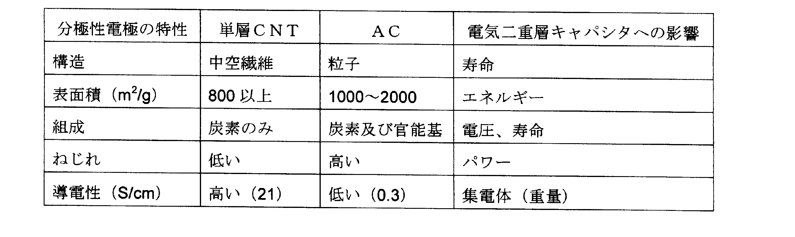
本実施形態において分極性電極として用いる分極性電極は、炭素純度が高く、金属不純物が少ないカーボンナノチューブ集合体により形成されることで高電圧条件下での動作を可能とし、電解液の化学反応が最小限に抑えられ、高導電性のカーボンナノチューブ集合体により形成されることで長寿命な電気二重層キャパシタを実現できる。また、高密度化され、適切な細孔経を有するカーボンナノチューブ集合体を用いることで、イオンの拡散を容易にし、高いパワーを有する電気二重層キャパシタを実現している。これにより、本発明に係る電気二重層キャパシタは、実施例に示すように3.5V以上4.5V未満の駆動電圧で駆動することができる。さらに、高導電性を有するカーボンナノチューブ集合体を用いることで、分極性電極が集電体としても機能し、電荷が分極性電極110の内部を垂直方向のみならず水平方向にも流れる。そのため、従来のような集電体を用いる必要がなく、軽量且つ小型の電気二重層キャパシタを提供できる。したがって、本実施形態に係る本発明の電気二重層キャパシタは、高電圧で、且つ、長寿命に動作させることが出来き、且つ、従来の電気二重層キャパシタに比して大きな電気密度、パワー密度を有する。
上述した本発明に係る電気二重層キャパシタの例について、以下に詳細に説明する。なお、以下の実施例は、一例であって本発明の電気二重層キャパシタはこれらに限定されるものではない。
(実施例1)
図2に本発明の実施例に係る電気二重層キャパシタ200の模式図を示す。
図2に本発明の実施例に係る電気二重層キャパシタ200の模式図を示す。
本実施例に係る本発明の電気二重層キャパシタ200は、第1の分極性電極と第2分極性電極として2つの分極性電極110と、イオン透過性のセパレータ120と、バリア部材160と、を有している。また、本実施例に係る本発明の電気二重層キャパシタ200は、電荷を取り出すための電極231及び外部電極用端子240を備える。本実施例に係る本発明の電気二重層キャパシタ200においては、2つの分極性電極110による第1の分極性電極と第2分極性電極との間にセパレータ120が対向するように配設され、対向する分極性電極110の外側の側面の一部分にカーボンナノチューブ集合体のCNTナノチューブの配向方向に垂直に延伸させた形状で、電極231を対向するように配設している。また、電極231には配列して設けられた外部電極用端子240を備え、分極性電極110には電解液が浸設している。この構成により分極性電極110、電極231及び外部電極用端子240の間での電気的な接続が構成される。バリア部材160は、分極性電極110、セパレータ120及び電極231を囲うように配設されており、バリア部材160によって電解液を分極性電極110及びセパレータ120に封入することができる。図2には、電気二重層キャパシタ200は、第1の分極性電極及び第2分極性電極の外側の側面の端部に電極231を配置した一例を示した。なお、図2は、内部の構成を説明のため、上面及び手前のバリア部材160は図示していない。
(製造方法)
以下に、電気二重層キャパシタ200の製造方法を具体的に説明する。本発明の実施例1に係る電気二重層キャパシタ200は、その動作電圧が3.5V以上4.5V未満であり、単層CNTを用いている。電極231は分極性電極110の側面の全面を覆わないため、分極性電極110が集電体としての役割を果たし、図2の矢印に示すように、電荷が分極性電極110の内部を水平方向かつ垂直方向に流れ、電極231へ向けて流れる。
以下に、電気二重層キャパシタ200の製造方法を具体的に説明する。本発明の実施例1に係る電気二重層キャパシタ200は、その動作電圧が3.5V以上4.5V未満であり、単層CNTを用いている。電極231は分極性電極110の側面の全面を覆わないため、分極性電極110が集電体としての役割を果たし、図2の矢印に示すように、電荷が分極性電極110の内部を水平方向かつ垂直方向に流れ、電極231へ向けて流れる。
図3は実施例1に係る電気二重層キャパシタ200の製造工程S100を示し、図3(a)は実施例1に係る電気二重層キャパシタ200の製造工程S100のフローチャートであり、図3(b)はその模式図である。製造工程S100は、例えば、分極性電極として用いるカーボンナノチューブ集合体の形成工程S110、カーボンナノチューブ集合体の剥離工程S120、カーボンナノチューブ集合体の乾燥工程S130、カーボンナノチューブ集合体の剪断工程S140、分極性電極組立工程S150及びカーボンナノチューブ集合体の高密度化工程S160を有する。
カーボンナノチューブ集合体の形成工程S110は、基板面に対して垂直方向に配向したカーボンナノチューブ集合体を形成する工程である。実施例1に係るカーボンナノチューブ集合体の形成工程S110においては、本発明者らが以前に報告した、水蒸気を添加した条件下で行うCVD法であるスーパーグロース法を用いてカーボンナノチューブ集合体を形成した。カーボンナノチューブ集合体30は、基板10に触媒粒子(図示せず)を形成し、触媒粒子から単層CNT31が基板面に対して垂直方向に成長することで形成される。
カーボンナノチューブ集合体30を形成するための基板10としては、その表面にCNTを成長させる触媒を担持することのできる非金属部材であり、400℃以上の高温でも形状を維持できるものであれば適宜のものを用いることができる。実施例1においては、基板10として、10mm×10mmのシリコン基板を用いた。
実施例1においては、触媒として鉄を、助触媒としてアルミナ(Al2O3)を用いた。基板表面への触媒層の形成には、高周波スパッタリング蒸着法を用いた。基板10の上部表面に、アルミナ(Al2O3)からなる厚さ10nmの助触媒層を形成し、アルミナ層上に鉄(Fe)からなる厚さ1nmの触媒層を形成した(S112)。このように触媒層を形成した基板を還元して、触媒粒子を形成した。
触媒層を形成した基板10を炉内圧力:1.02×10⁵Paに保持されたCVD装置の合成炉内に搬送・設置し、合成炉内のガス流量の総量が1000sccmとなるように、雰囲気ガスとしてHeを600sccm、還元ガスとしてH2を400sccmの割合で、15分間でガス供給管から導入した。この15分間で炉内温度を室温から750℃まで昇温した。
次に、炉内温度:750℃、炉内圧力:1.02×10⁵Pa(大気圧)に保持された状態の合成炉内に、He(雰囲気ガス):510sccm、H2(還元ガス):400sccm、H2O含有He(相対湿度23%)(キャリアガスに混入した触媒賦活物質):90sccmを、5分間供給することで水分添加処理を行った。
つづいて、炉内温度:750℃、炉内圧力:1.02×10⁵Pa(大気圧)に保持された状態の合成炉内に、ガス流量の総量が1000sccmとなるようにHe(雰囲気ガス):850sccm、エチレン(C2H4)(原料ガス):100sccm、H2O含有He(相対湿度23%)(キャリアガスに混入した触媒賦活物質):50sccmを10分間供給することでCNT31を形成し、カーボンナノチューブ集合体30を得た。本実施例においては、カーボンナノチューブ集合体30の密度は、0.03g/ccであった。
このようにして得たカーボンナノチューブ集合体30を基板10に形成した触媒粒子から剥離する(S120)。カーボンナノチューブ集合体30の剥離は、例えば、ピンセットを用いてカーボンナノチューブ集合体30を基板10に対して水平方向に軽く押すことで行うことができる。剥離されたカーボンナノチューブ集合体30は、面積が10mm×10mm、厚さが500μm~1mmであり、炭素純度99.9%、金属不純物が0.013mass%で、比表面積が1100m2/gであった。カーボンナノチューブ集合体は500μm~1mmの長さであることで結合力を有し、高密度化を可能にする。
ここで、カーボンナノチューブ集合体30に金属粒子が残存すると高電圧下で反応を起こすため、鉄触媒のような金属粒子をカーボンナノチューブ集合体30に残存させないように、基板10に形成した触媒粒子からカーボンナノチューブ集合体30を剥離することが重要である。本発明に係る実施例1のカーボンナノチューブ集合体30は基板10上に形成した触媒粒子から単層CNT31を成長させているため、上述のカーボンナノチューブ集合体の剥離工程においては、触媒粒子が基板10上から脱離することが殆ど無く、カーボンナノチューブ集合体30に触媒粒子が殆ど残存しない。
次に、剥離したカーボンナノチューブ集合体30は150℃で8時間以上かけて真空乾燥させた(S130)。不活性環境下(グローブボックスをアルゴンで満たし、酸素濃度2ppm以下、露点温度-80℃以下)で、真空乾燥したカーボンナノチューブ集合体30は、垂直方向に配向したカーボンナノチューブ集合体30を水平方向に配向した単層CNT配向シート35に変形するように、スライドガラス40の間で剪断することで準高密度化(密度:0.2g/cc)する(S140)。ここで、高電圧で動作させるためには分極性電極110内の湿気や酸素の残存量を最小限にすることが重要である。したがって、これ以降の工程は上述の不活性環境下で行う必要がある。
同じ重さと厚さ(9mm×9mm×0.075mm)を有する2枚の準高密度化した単層CNT配向シート35が互いに向かい合うように、セパレータ120として用いる厚さ40μmのセルロースの多孔質紙を挟み、電気二重層キャパシタ200を組立てる(S150)。つづいて、2枚の単層CNT配向シート35の端部にプラチナメッシュの電極231をそれぞれ配置する。電極231の接触面積は分極性電極110の外側側面の総表面積の5%である。電極231は分極性電極110の側面の全面を覆わないため、分極性電極110が集電体としての役割を果たし、電荷が分極性電極110内部を水平方向かつ垂直方向に電極231へ向けて流れる。
ここで、2つの分極性電極110には同じ大きさの電圧(本実施例においては、2V+2V)を印加するため、同じ重さ(同じ厚さ)の分極性電極を用いることが重要である。一方の電極が他方の電極よりも重い(厚い)と、不均一な電圧分布となり、軽い(薄い)電極に過剰な電流が流れ、キャパシタが破損する。
組立てた電気二重層キャパシタ200は有機系電解液で満たし、単層CNT配向シート35を高密度化する。本発明の本実施例に係る電気二重層キャパシタ200においては、水系電解液よりも有機系電解液を用いることが望ましい。有機系電解液を用いることで、高電圧条件下での動作が可能となる。高密度化に用いる有機系電解液には、電気二重層キャパシタ200の分極性電極110及びセパレータ120に封入する電解液と同じ電解液を用い、本実施例においては、1M テトラフルオロホウ酸テトラエチルアンモニウムの炭酸プロピレン溶液を用いた。分極性電極110に電解液を完全に浸透させ、キャパシタ内の気体を完全に取り除くために、電気二重層キャパシタ200は真空下(100Torr以下)に30分間置いた。電解液を浸透させることで、準高密度化した単層CNT配向シート35が高密度化されて分極性電極110となり、電極表面への良好なイオンアクセスが確保される。ここで重要なのは、分極性電極110に電解液を浸透させることである。電解液以外の液体で分極性電極の高密度化を行うと、真空乾燥後にも残存した液体が単層CNTの表面に吸収された状態となり、残存した液体が高電圧で反応し、4Vでの電気二重層キャパシタの動作を阻害することとなる。
このようにして得られた分極性電極110を構成する、高密度化処理されたカーボンナノチューブ集合体の特性は、溶媒(炭酸プロピレン溶液)のみを用いて高密度化処理を施した、カーボンナノチューブ集合体の特性を計測することで、評価できる。本実施例で用いた、高密度化処理を施した、カーボンナノチューブ集合体は導電性が20S/cm、単層CNT含有率が99%、密度が0.5g/cm3、G/D比が2.5~40、BET-比表面積が1100m2/g、平均外径が2.8nm、半値幅2nm、炭素純度が99.9mass%、金属不純物が0.013mass%、細孔経の分布極大が4nm、ヘルマンの配向係数0.7であった。分極性電極110は、導電性が7S/cmであり、分極させた後は、導電性が300S/cmであった。また、金属不純物の含有量は0.008mass%であり、重量密度は0.93g/cm3である。
本発明の本実施例に係る分極性電極として、上述した高純度、且つ高導電性のカーボンナノチューブ集合体で形成した分極性電極110を用いる。これにより、電気二重層キャパシタの電解液中のイオンアクセスが向上し、後述するように、高電圧条件下で使用可能な電気二重層キャパシタを提供することができる。このように組立てた電気二重層キャパシタ200は、バリア部材160を配置し、電解液を封入する。バリア部材160は電解液を密閉できる形態、材料であればよく、従来のシール材のみで形成することができ、例えば、ポリイミドフィルムのような様々なポリマーやプラスチックを適用できる。また、電気二重層キャパシタ200の機能を制限するものでなく、化学的に安定で、軽量な物質であれば、これらに限定されるものではない。本実施形態の電気二重層キャパシタ200の分極性電極110及びセパレータ120に封入する電解液には、有機系電解液を用いることが好ましい。本実施例においては、単層CNT配向シート35の高密度化に用いた1M テトラフルオロホウ酸テトラエチルアンモニウムの炭酸プロピレン溶液を用いた。電気二重層キャパシタ200は、有機系電解液を用いることで、高電圧での長寿命の動作が可能となる。
図2に示したように、本実施例の分極性電極110は、カーボンナノチューブ集合体がセパレータ120に対して平行な方向に配向するよう配置し、分極性電極110の側面に部分的に電極231を接続する。分極性電極として用いる分極性電極110は、高純度、且つ高導電性のカーボンナノチューブ集合体を用いることで優れ電気特性を示し、電極としての機能と集電体としての機能とを有する。従来の電気二重層キャパシタにおいては、集電体を対向するように配設された一対のAC電極の側面全面に配置する必要があった。分極性電極110に高純度のカーボンナノチューブ集合体を用いることで、導電性が高く、電解液中のイオンアクセスが良好となり、分極性電極110は集電体としても機能するため、電気二重層キャパシタ200は、従来の電気二重層キャパシタとは異なり、分極性電極110の側面に部分的に電極231を接続することで、高電圧条件下でも動作が可能となる。つまり、本発明の本実施例に係る電極231は、分極性電極110から電荷を取り出す機能があればよく、集電体としての機能は必要としない。したがって、本発明の本実施例に係る電気二重層キャパシタ200は、集電体としての機能も有する分極性電極110と、電極231とを組合せることで、集電体を必要とする従来の電気二重層キャパシタに比して、軽量且つ小型な電気二重層キャパシタを提供することができる。
本発明の本実施例に係る電極231には、アルミニウムやプラチナ等の金属や、その金属合金、窒化チタン等の金属化合物、poly 3-methyl thiophene等の導電性ポリマー、CNTゴムなどを用いることができる。また、電極231は、薄膜でも網目状の部材でもよく、直流導電率が100S/cm以上、または、シート抵抗が1 ohm/square以下の部材を用いるとよい。
電極231の接触面積及び厚さは、用いる部材により異なり、分極性電極内を流れる電荷を集められればよく、電極231の接触面積は上述した分極性電極110の側面の一部分に相当する面積で良い。また、電極231を分極性電極110に蒸着させる場合には、スパッタリング、抵抗加熱蒸着や電子ビーム蒸着等の物理蒸着やCVDのいずれも用いることができる。図2において、電極231はセパレータ120を間に配設した2つの分極性電極110の端部に対向するように配置しているが、電極231の配置はこれに限定されるものではなく、電極231の配置は分極性電極内を流れる電荷を集められれば、前後左右、適宜変更可能である。したがって、本実施例に係る電気二重層キャパシタ200は、従来の集電体に代えて、電極231を用いることで、軽量、且つ、薄型の電気二重層キャパシタを提供することができる。なお、電極231は、分極性電極110の側面の全面を覆ってもよい。
集電体は電極内の電位を均一にする働きをし、電極内の電位の分布を電極の厚さ方向のみに存在させる。一方、電気二重層キャパシタ200は、電極231を用いることで、電極内の電位の分布が電極全体にわたることになる。このような電極231をAC電極に用いた場合、AC電極の導電性が低いため、電極内を流れる電荷を集めることができなくなり、従来の電気二重層キャパシタは動作できなくなる。実施例1の本発明に係る電気二重層キャパシタ200は、分極性電極110が集電体としての機能も担い、分極性電極110がAC電極より優れた導電性を有することで、電極231が適用可能となる。
本実施例において分極性電極として用いる分極性電極は、炭素純度が高く、金属不純物が少ないカーボンナノチューブ集合体により形成されることで高電圧条件下での動作を可能とし、電解液の化学反応が最小限に抑えられ、高導電性のカーボンナノチューブ集合体により形成されることで長寿命な電気二重層キャパシタを実現できる。また、高密度化され、適切な細孔経を有するカーボンナノチューブ集合体を用いることで、イオンの拡散を容易にし、高いパワーを有する電気二重層キャパシタを実現している。これにより、本実施に係る電気二重層キャパシタは、実施例に示すように3.5V以上4.5V未満の駆動電圧で駆動することができる。さらに、高導電性を有するカーボンナノチューブ集合体を用いることで、分極性電極が集電体としても機能し、電荷が分極性電極110の内部を垂直方向のみならず水平方向にも流れる。
そのため、従来のような集電体を用いる必要がなく、分極性電極に接続する電極は電荷を出し入れする機能があればよく、軽量且つ小型の電気二重層キャパシタを提供できる。したがって、本実施形態に係る本発明の電気二重層キャパシタは、高電圧で、且つ、長寿命に動作させることが出来き、且つ、従来の電気二重層キャパシタに比して大きな電気密度、パワー密度を有する。
(実施例2)
本実施例においては、実施例1の変形例として、分極性電極として用いる分極性電極110の側面に部分的に電極335を複数接続して、複数の異なる箇所で、分極性電極110と電気的に接続された、電気二重層キャパシタ300を構成する例について説明する。このようにすれば、大型の分極性電極110においても、側面全面を覆う集電体を用いることなしに、分極性電極110を流れる電荷を効率良く集めることができ、好適である。図4に本発明の実施例2に係る電気二重層キャパシタ300の模式図を示す。電気二重層キャパシタ300は、セパレータ120を2つの分極性電極110(第1の分極性電極及び第2分極性電極)で挟み込む。分極性電極110の外側の側面に部分的に電極335を複数接続し、外部電極用端子240(図示せず)をそれぞれ接続する。分極性電極110は電解液で満たされている。この構成により分極性電極110、電極335及び外部電極用端子240の間での電気的な接続が構成される。バリア部材160は、分極性電極110、セパレータ120及び電極335を囲うように配設されており、バリア部材160によって電解液を分極性電極110及びセパレータ120に封入することができる。なお、図4は、内部の構成を説明のため、バリア部材160は図示していない。なお、外部電極用端子240は、分極性電極110を覆う電気二重層キャパシタ300のバリア部材160のパッケージにプリントした回路としてもよい。
本実施例においては、実施例1の変形例として、分極性電極として用いる分極性電極110の側面に部分的に電極335を複数接続して、複数の異なる箇所で、分極性電極110と電気的に接続された、電気二重層キャパシタ300を構成する例について説明する。このようにすれば、大型の分極性電極110においても、側面全面を覆う集電体を用いることなしに、分極性電極110を流れる電荷を効率良く集めることができ、好適である。図4に本発明の実施例2に係る電気二重層キャパシタ300の模式図を示す。電気二重層キャパシタ300は、セパレータ120を2つの分極性電極110(第1の分極性電極及び第2分極性電極)で挟み込む。分極性電極110の外側の側面に部分的に電極335を複数接続し、外部電極用端子240(図示せず)をそれぞれ接続する。分極性電極110は電解液で満たされている。この構成により分極性電極110、電極335及び外部電極用端子240の間での電気的な接続が構成される。バリア部材160は、分極性電極110、セパレータ120及び電極335を囲うように配設されており、バリア部材160によって電解液を分極性電極110及びセパレータ120に封入することができる。なお、図4は、内部の構成を説明のため、バリア部材160は図示していない。なお、外部電極用端子240は、分極性電極110を覆う電気二重層キャパシタ300のバリア部材160のパッケージにプリントした回路としてもよい。
本発明の実施例2に係る電気二重層キャパシタ300には、実施例1で説明した分極性電極110、セパレータ120及び電解液を用いることができ、それぞれの詳細については、ここでは省略する。本発明の実施例2に係る電極335には、分極性電極110の側面に実施例1の電極231と同様の部材を用いて形成することができる。電極335の接触面積及び厚さは用いる部材により異なるが、分極性電極内を流れる電荷を集められればよく、電極335の総接触面積は、セパレータ120を介して対向する分極性電極110の側面の一部分に相当する面積でよい。また、電極335を分極性電極110に蒸着させる場合には、スパッタリング、抵抗加熱蒸着や電子ビーム蒸着等の物理蒸着やCVDのいずれも用いることができる。電極335はセパレータ120を間に配設した2つの分極性電極110の外側の側面にそれぞれ対称に配置してもよく、非対称に配置してもよい。
従来の電気二重層キャパシタはセパレータを介して対向するように配置された電極の側面全体に集電体を配置していた。一方、実施例2の電極335は、分極性電極内を流れる電荷を集められればよく、分極性電極110の側面に小さなスポットとして分散配置することができるため、集電体に比して総面積が遥かに小さい。したがって、実施例2の本発明に係る電気二重層キャパシタ300は、電極335を用いることで、従来の電気二重層キャパシタよりも軽量且つ薄い電気二重層キャパシタを実現できる。
集電体は、電極内の電位を均一にする働きをし、電極内の電位の分布を電極の厚さ方向のみに存在させる。一方、電気二重層キャパシタ300は、集電体としての機能も有する分極性電極110と、電極335とを組合せることで、電極内の電位の分布が電極全体にわたることになる。このような電極335をAC電極に用いた場合、従来の電気二重層キャパシタは動作できなくなる。実施例2の本発明に係る電気二重層キャパシタ300は、分極性電極110が集電体としての機能も担い、分極性電極110がAC電極より優れ電気特性を有することで、電極335が適用可能となる。
以上説明したように、本実施例に係る電気二重層キャパシタは、炭素純度が高く、金属不純物が少ないカーボンナノチューブ集合体により形成されることで高電圧条件下での動作を可能とし、電解液の化学反応が最小限に抑えられ、高導電性のカーボンナノチューブ集合体により形成されることで長寿命な電気二重層キャパシタを実現できる。また、高密度化され、適切な細孔経を有するカーボンナノチューブ集合体を用いることで、イオンの拡散を容易にした高導電性のカーボンナノチューブ集合体により形成された分極性電極が提供されることで、図4の矢印に示すように、電荷が分極性電極110の内部を垂直方向のみならず水平方向にも流れる。そのため、従来のような集電体を用いる必要がなく、分極性電極110に部分的に接続される電極は電荷を出し入れする機能があればよく、軽量且つ小型の電気二重層キャパシタを提供することができる優れた効果を奏する。また、本発明の実施例に係る電気二重層キャパシタは、高電圧で、且つ、長寿命で動作させることが出来き、且つ、従来の電気二重層キャパシタに比して大きな電気密度、パワー密度を有する。これにより、本実施に係る電気二重層キャパシタは、実施例に示すように3.5V以上4.5V未満の駆動電圧で駆動することができる。なお、実施例1及び2において説明した電圧印加用部材は、組合せて用いてもよい。すなわち、電気二重層キャパシタの一方の分極性電極に実施例1の電極231を用い、もう一方の分極性電極に実施例2の電極335を用いるような組み合わせでもよい。
(実施例3)
本実施例においては、本発明に係る分極性電極として用いる分極性電極110に従来の集電体を適用した電気二重層キャパシタ400について説明する。図5に本発明の実施例3に係る電気二重層キャパシタ400の模式図を示す。電気二重層キャパシタ400は、セパレータ120を2つの分極性電極110(第1の分極性電極及び第2分極性電極)で挟み込む。2つの分極性電極110の外側の側面全体に2枚の集電体450を対向するように配置し、外部電極用端子240を接続する。分極性電極110は電解液で満たされている。この構成により分極性電極110、集電体450及び外部電極用端子240の間での電気的な接続が構成される。バリア部材160は、分極性電極110、セパレータ120及び集電体450を囲うように配設されており、バリア部材160によって電解液を分極性電極110及びセパレータ120に封入することができる。なお、図5は、内部の構成を説明のため、上面及び手前のバリア部材160は図示していない。
本実施例においては、本発明に係る分極性電極として用いる分極性電極110に従来の集電体を適用した電気二重層キャパシタ400について説明する。図5に本発明の実施例3に係る電気二重層キャパシタ400の模式図を示す。電気二重層キャパシタ400は、セパレータ120を2つの分極性電極110(第1の分極性電極及び第2分極性電極)で挟み込む。2つの分極性電極110の外側の側面全体に2枚の集電体450を対向するように配置し、外部電極用端子240を接続する。分極性電極110は電解液で満たされている。この構成により分極性電極110、集電体450及び外部電極用端子240の間での電気的な接続が構成される。バリア部材160は、分極性電極110、セパレータ120及び集電体450を囲うように配設されており、バリア部材160によって電解液を分極性電極110及びセパレータ120に封入することができる。なお、図5は、内部の構成を説明のため、上面及び手前のバリア部材160は図示していない。
本発明の実施例3に係る電気二重層キャパシタ400には、実施例1で説明した分極性電極110、セパレータ120及び電解液を用いることができ、それぞれの詳細については、ここでは省略する。実施例3の電気二重層キャパシタ400は、図5に示したように、集電体450を備えること以外は電気二重層キャパシタ200と同様の構成である。したがって、9mm×9mm×0.075mmの大きさの2枚の準高密度化した単層CNT配向シート35が互いに向かい合うように、厚さ40μmのセルロースの多孔質紙のセパレータ120を挟む組立工程までは、電気二重層キャパシタ200と同様の製造方法を用いた。
セパレータ120を挟んだ2枚の単層CNT配向シート35の外側の側面に、2枚の集電体450を配置した。集電体450には、アルミニウムやプラチナ等の直流導電率が10000S/cm以上、または、シート抵抗が0.01 ohm/square以下の金属部材を用いることができる。集電体450の形状は薄膜でも網目状の部材でもよく、厚さは用いる部材により異なるが、分極性電極110の側面全体に形成する。
このようにして組立てた電気二重層キャパシタ400を実施例1と同様に、1M テトラフルオロホウ酸テトラエチルアンモニウムの炭酸プロピレン溶液を用いて高密度化することで分極性電極110を形成した。
分極性電極110を構成する、高密度化処理されたカーボンナノチューブ集合体の特性は、溶媒(炭酸プロピレン溶液)のみを用いて高密度化処理を施した、カーボンナノチューブ集合体の特性を計測することで、評価できる。本実施例で用いた、高密度化処理を施した、カーボンナノチューブ集合体は導電性が20S/cm、単層CNT含有率が99%、密度が0.5g/cm3、G/D比が2.5~40、BET-比表面積が1100m2/g、平均外径が2.8nm、半値幅2nm、炭素純度が99.9mass%、金属不純物が0.013mass%、細孔経の分布極大が4nm、ヘルマンの配向係数0.7であった。このようにして得られた分極性電極110は、導電性が7S/cmであり、分極させた後は、導電性が300S/cmであった。また、金属不純物の含有量は0.008mass%であり、重量密度は0.93g/cm3である。
電気二重層キャパシタ400は、従来の集電体450を用いるため、実施例1及び2で説明した電気二重層キャパシタ程は軽量且つ小型の電気二重層キャパシタにはならない。しかし、本実施例に係る電気二重層キャパシタ400は、分極性電極110の側面全体に集電体450を配置することで、分極性電極110内の電位を均一にする働きをし、分極性電極110内の電位の分布を電極の厚さ方向のみに存在させる。そのため、電荷が分極性電極110の内部を垂直方向のみに流れる。そのため、電気二重層キャパシタ400は、電圧印加用部材を用いた実施例1及び2に係る電気二重層キャパシタに比して集電効率が高い。このため、電気二重層キャパシタ400は、高電圧で作動する大容量のキャパシタに好適に用いることができ、電極を用いた電気二重層キャパシタ400よりも、大型化しても性能の劣化が少なく好適である。
また、薄膜の集電体450に代えて、分極性電極110の側面に網目状の部材である電極を用いた場合、集電体450で形成した電気二重層キャパシタよりも軽量化することができる。本実施例においては、集電体450としてプラチナメッシュを用いた。
以上説明したように、本実施例に係る電気二重層キャパシタは、炭素純度が高く、金属不純物が少ないカーボンナノチューブ集合体により形成されることで高電圧条件下での動作を可能とし、電解液の化学反応が最小限に抑えられ、高導電性のカーボンナノチューブ集合体により形成されることで長寿命な電気二重層キャパシタを実現できる。また、高密度化され、適切な細孔経を有するカーボンナノチューブ集合体を用いることで、イオンの拡散を容易にし、高いパワーを有する電気二重層キャパシタを実現している。高導電性のカーボンナノチューブ集合体により形成された分極性電極と、集電効率が高い集電体とを組み合わせることで、大容量の電気二重層キャパシタを提供する優れた効果を奏する。また、本発明の実施例に係る電気二重層キャパシタは、高電圧で、且つ、長寿命で動作させることが出来き、且つ、従来の電気二重層キャパシタに比して大きな電気密度、パワー密度を有する。これにより、本実施に係る電気二重層キャパシタは、実施例に示すように3.5V以上4.5V未満の駆動電圧で駆動することができる。上述したように、高導電性を有するカーボンナノチューブ集合体を用いることで、分極性電極が集電体としても機能し、電荷が分極性電極110の内部を垂直方向のみならず水平方向にも流れる。そのため、従来のような集電体を用いる必要がなく、電荷を出し入れする機能を有する網目状の電極を用いることもでき、集電体を用いた場合よりも軽量化することができる。
(実施例4)
電気二重層キャパシタは、出力電圧を増加させるために複数のキャパシタを積層した構造を形成する。そのため、隣接したキャパシタ間の電気的な接触(オーミックコンタクト)は必要であるが、隣接したキャパシタ間のイオン的な接触(電解液の流れ)を防ぐ必要がある。従来のAC電極では導電性が低いため、金属層(一般的にはアルミニウム)の集電体で電極の側面全体を覆っており、この集電体が隣接したキャパシタ間のイオン的な接触を防ぐ役割も担っている。本実施例においては、出力電圧を増加させるために、実施形態で説明した集電体を有さない電気二重層キャパシタを積層する方法について説明する。
電気二重層キャパシタは、出力電圧を増加させるために複数のキャパシタを積層した構造を形成する。そのため、隣接したキャパシタ間の電気的な接触(オーミックコンタクト)は必要であるが、隣接したキャパシタ間のイオン的な接触(電解液の流れ)を防ぐ必要がある。従来のAC電極では導電性が低いため、金属層(一般的にはアルミニウム)の集電体で電極の側面全体を覆っており、この集電体が隣接したキャパシタ間のイオン的な接触を防ぐ役割も担っている。本実施例においては、出力電圧を増加させるために、実施形態で説明した集電体を有さない電気二重層キャパシタを積層する方法について説明する。
集電体は双極性の板で、このような集電体を追加すると、電気二重層キャパシタ全体の重量が増加する。また、集電体のシール性と耐腐食性の要求は、電気二重層キャパシタの構成を複雑にする。さらに、集電体は金属であるため熱伝導性が高く、1つのキャパシタが破損し熱が放出されると、積層された電気二重層キャパシタ全体に破損の影響が及ぶこととなる。
本実施例においては、双極性の集電体を必要としない、バリア部材を介して隣接する分極性電極110を電気的に接続する電気二重層キャパシタ500を示す。本発明の実施例4に係る電気二重層キャパシタ500には、実施例1で説明した分極性電極110、セパレータ120及び電解液を用いることができ、それぞれの詳細については、ここでは省略する。
図6は電気二重層キャパシタ500の模式図である。電気二重層キャパシタ500は、2つの分極性電極110の間にセパレータ120が対向するように配設された電気二重層キャパシタがバリア部材563を介して積層される。バリア部材160は、分極性電極110、セパレータ120及びバリア部材563を囲うように配設されており、バリア部材160によって電解液を分極性電極110及びセパレータ120に封入することができる。なお、図6は、内部の構成を説明のため、上面及び手前のバリア部材160は図示していない。バリア部材563には、例えば、poly 3-methyl thiophene等の導電性ポリマー、CNTゴムなどの柔軟なプラスチック導電体の薄膜を用いることができる。バリア部材563は、シール性を有し、酸素や酸化物を含まず、電気化学的に安定で100S/cm以上の直流導電率を有する部材であれば、これらに限定されるものではない。電気二重層キャパシタ500は、導電性を有するバリア部材563を用いることで、隣接する分極性電極110を電気的に接続することができる。また、本実施例に係るバリア部材563は、集電体に比して直流導電率が高くはないが、導電性に優れた分極性電極110を用いることで動作を可能にする。
上述したように、分極性電極110は双極性の集電体を必要としないため、導電性の低いバリア部材563を用いても積層した電気二重層キャパシタ500形成することができる。バリア部材563には金属を用いないため柔軟性に富み、したがって、バリア部材563を用いた本実施例に係る電気二重層キャパシタ500も、従来の積層した電気二重層キャパシタに比して柔軟性を有し、製品としての電気二重層キャパシタの形状に制約を受けない。
以上説明したように、本実施例に係る電気二重層キャパシタは、炭素純度が高く、金属不純物が少ないカーボンナノチューブ集合体により形成されることで高電圧条件下での動作を可能とし、電解液の化学反応が最小限に抑えられ、高導電性のカーボンナノチューブ集合体により形成されることで長寿命な電気二重層キャパシタを実現できる。また、本発明の実施例に係る電気二重層キャパシタは、高電圧で、且つ、長寿命で動作させることが出来き、且つ、従来の電気二重層キャパシタに比して大きな電気密度、パワー密度を有する。これにより、本実施に係る電気二重層キャパシタは、実施例に示すように3.5V以上4.5V未満の駆動電圧で駆動することができる。高密度化され、適切な細孔経を有するカーボンナノチューブ集合体を用いることで、イオンの拡散を容易にした高導電性のカーボンナノチューブ集合体により形成された分極性電極が提供されることで、電荷が分極性電極の内部を垂直方向のみならず水平方向にも流れる。そのため、従来のような集電体を用いる必要がなく、集電体に代わって電荷を出し入れする機能を有する導電性のバリア部材を組合せて用いて電気二重層キャパシタを積層することができるため、従来に比して軽量かつ小型で柔軟な電気二重層キャパシタを提供する優れた効果を奏する。また、シール層は金属に比して熱伝導性が低いため、隣接する電気二重層キャパシタへの熱伝導を制限し、1つの電気二重層キャパシタが破損しても隣接する電気二重層キャパシタへの影響を最小限にすることができる。
(実施例5)
実施例4においては、バリア部材を介して隣接する分極性電極110をシールする電気二重層キャパシタについて説明したが、本実施例においては、本発明に係る分極性電極110に従来の集電体を用いる電気二重層キャパシタについて説明する。本発明の実施例5に係る電気二重層キャパシタ600には、実施例1で説明した分極性電極110、セパレータ120及び電解液を用いることができ、それぞれの詳細については、ここでは省略する。
実施例4においては、バリア部材を介して隣接する分極性電極110をシールする電気二重層キャパシタについて説明したが、本実施例においては、本発明に係る分極性電極110に従来の集電体を用いる電気二重層キャパシタについて説明する。本発明の実施例5に係る電気二重層キャパシタ600には、実施例1で説明した分極性電極110、セパレータ120及び電解液を用いることができ、それぞれの詳細については、ここでは省略する。
図7は電気二重層キャパシタ600の模式図である。電気二重層キャパシタ600は、2つの分極性電極110の間にセパレータ120が対向するように配設された電気二重層キャパシタが集電体675を介して積層される。バリア部材160は、分極性電極110、セパレータ120及び集電体675を囲うように配設されており、バリア部材160によって電解液を分極性電極110及びセパレータ120に封入することができる。なお、図7は、内部の構成を説明のため、上面及び手前のバリア部材160は図示していない。集電体675には、実施例3で説明した集電体と同様に、アルミニウムやプラチナ等の直流導電率が10000S/cm以上、または、シート抵抗が0.01 ohm/square以下の金属部材を用いることができる。ただし、集電体675はシール性を要求されるため、網目状の部材を用いることはできない。電気二重層キャパシタ600は、集電体675を用いることで、シール性を確保しつつ、隣接する分極性電極110を電気的に接続することができる。また、本実施例に係る電気二重層キャパシタ600は集電体675を用いることで、バリア部材を用いた実施例4の電気二重層キャパシタ程は軽量で柔軟ではないが、導電性に優れた分極性電極と、集電効率が高い集電体とを組み合わせることで、大容量の電気二重層キャパシタを提供することができる。
本実施例に係る電気二重層キャパシタは、炭素純度が高く、金属不純物が少ないカーボンナノチューブ集合体により形成されることで高電圧条件下での動作を可能とし、電解液の化学反応が最小限に抑えられ、高導電性のカーボンナノチューブ集合体により形成されることで長寿命な電気二重層キャパシタを実現できる。また、高密度化され、適切な細孔経を有するカーボンナノチューブ集合体を用いることで、イオンの拡散を容易にし、高いパワーを有する電気二重層キャパシタを実現している。これにより、本実施に係る電気二重層キャパシタは、実施例に示すように3.5V以上4.5V未満の駆動電圧で駆動することができる。高導電性のカーボンナノチューブ集合体により形成された分極性電極と、集電効率が高い集電体とを組み合わせることで、積層した大容量の電気二重層キャパシタを提供する優れた効果を奏する。また、本発明の実施例に係る積層した電気二重層キャパシタは、高電圧で、且つ、長寿命で動作させることが出来き、従来の電気二重層キャパシタに比して大きな電気密度、パワー密度を有する。
以上説明したように、本発明の実施例1~5に係る電気二重層キャパシタは、炭素純度が高く、金属不純物が少ないカーボンナノチューブ集合体により形成されることで高電圧条件下での動作を可能とし、電解液の化学反応が最小限に抑えられ、高導電性のカーボンナノチューブ集合体により形成されることで長寿命な電気二重層キャパシタを実現できる。また、高密度化され、適切な細孔経を有するカーボンナノチューブ集合体を用いることで、イオンの拡散を容易にし、高いパワーを有する電気二重層キャパシタを実現している。さらに、高導電性を有するカーボンナノチューブ集合体を用いることで、分極性電極が集電体としても機能し、集電体を用いずに電気二重層キャパシタ構成することもでき、軽量且つ小型の電気二重層キャパシタを提供することができる。
(比較例1)
(従来のAC電極を用いた電気二重層キャパシタの製造方法)
比較例1として、従来のAC電極を用いた電気二重層キャパシタを製造した。比較例1の電気二重層キャパシタ700(図示せず)は、分極性電極110の代わりにAC電極710を用いた以外は実施例3の電気二重層キャパシタ400と同様の構成である。図16(a)はAC電極710の製造工程を示す模式図であり、図16(b)はAC電極710のSEM像である。
(従来のAC電極を用いた電気二重層キャパシタの製造方法)
比較例1として、従来のAC電極を用いた電気二重層キャパシタを製造した。比較例1の電気二重層キャパシタ700(図示せず)は、分極性電極110の代わりにAC電極710を用いた以外は実施例3の電気二重層キャパシタ400と同様の構成である。図16(a)はAC電極710の製造工程を示す模式図であり、図16(b)はAC電極710のSEM像である。
AC電極710の製造には公知の材料であるAC粉末(以下、ACという)(クラレケミカル株式会社製、YP17、比表面積1640m2/g)、導電助剤としてカーボンブラック(Carbon black)及びバインダーとしてポリテトラフルオロエチレン(PTFE)を用いた。ACを80mass%、カーボンブラックを10mass%及びPTFEを10mass%で粉砕・混合してAC混合物を得た。次に、AC混合物をローラーで平板化し、さらに加圧・加熱成型してAC電極710を形成した。実施例6と同様に真空乾燥した後のAC電極710は、密度が0.6g/cc、比表面積1400m2/g、導電性が0.3S/cm、炭素純度99%以上、金属不純物1%以下、細孔経分布極大、1nm以上2nm以下、9mm×9mm×0.075mmの大きさで、このAC電極710を2枚用いて、実施例3と同様にセパレータ120、集電体450と組合せて比較例1の電気二重層キャパシタ700を製造した。
(比較例2)
(集電体を有しない従来のAC電極を用いた電気二重層キャパシタの製造方法)
比較例2として、比較例1で説明したAC電極710を用いて、実施例1の電気二重層キャパシタ200と同様の構成の電気二重層キャパシタ800を製造した。すなわち、比較例2の電気二重層キャパシタ800は、集電体450の代わりに電極231を用いる点で比較例1と異なる。
(集電体を有しない従来のAC電極を用いた電気二重層キャパシタの製造方法)
比較例2として、比較例1で説明したAC電極710を用いて、実施例1の電気二重層キャパシタ200と同様の構成の電気二重層キャパシタ800を製造した。すなわち、比較例2の電気二重層キャパシタ800は、集電体450の代わりに電極231を用いる点で比較例1と異なる。
(単層CNT電気二重層キャパシタの特性)
上述のように製造した実施例1、実施例3、比較例1及び比較例2の電気二重層キャパシタの特性をそれぞれ評価した。図8(a)は実施例1及び実施例3に用いた分極性電極110の側面から観察したSEM像である。分極性電極110は優れた配向性を有するカーボンナノチューブ集合体で形成されている。一方、図16(b)に示したように、AC電極710はACとカーボンブラックが不規則に配置して形成されている。
上述のように製造した実施例1、実施例3、比較例1及び比較例2の電気二重層キャパシタの特性をそれぞれ評価した。図8(a)は実施例1及び実施例3に用いた分極性電極110の側面から観察したSEM像である。分極性電極110は優れた配向性を有するカーボンナノチューブ集合体で形成されている。一方、図16(b)に示したように、AC電極710はACとカーボンブラックが不規則に配置して形成されている。
(実施例と比較例との対比)
図8(b)は0~4Vに分極した時の実施例1、実施例3及び比較例1のサイクリックボルタモグラム(Cyclic voltammogram:以下、CVプロットという)であり、横軸は電位を示し、縦軸は電流密度を示す。実施例1の電気二重層キャパシタ200及び実施例3の電気二重層キャパシタ400は対称なプロットを示し、分極させた電位範囲全体にわたり分極性電極が安定していることがわかる。一方、比較例1の電気二重層キャパシタ700は3V以上でピークのある非対称なプロットを示し、3V以上ではAC電極が破損することがわかる。また、図示しないが、実施例1の電気二重層キャパシタ200及び実施例3の電気二重層キャパシタ400は、4.5V以上では破損する。
図8(b)は0~4Vに分極した時の実施例1、実施例3及び比較例1のサイクリックボルタモグラム(Cyclic voltammogram:以下、CVプロットという)であり、横軸は電位を示し、縦軸は電流密度を示す。実施例1の電気二重層キャパシタ200及び実施例3の電気二重層キャパシタ400は対称なプロットを示し、分極させた電位範囲全体にわたり分極性電極が安定していることがわかる。一方、比較例1の電気二重層キャパシタ700は3V以上でピークのある非対称なプロットを示し、3V以上ではAC電極が破損することがわかる。また、図示しないが、実施例1の電気二重層キャパシタ200及び実施例3の電気二重層キャパシタ400は、4.5V以上では破損する。
次に、電極の容量と初期抵抗を確認するために充放電試験を行った。図9(a)は1A/gにおける3Vの定電流放電プロファイルを示し、図9(b)は、4Vの定電流放電プロファイルを示す。図9(a)に示すように、比較例2の電気二重層キャパシタ800は、集電体450がないため動作しなかった。また、図9(b)に示すように、4Vの放電プロファイルにおいても、実施例1の電気二重層キャパシタ200及び実施例3の電気二重層キャパシタ400は、比較例1の電気二重層キャパシタ700に比して良好な放電プロファイルを示した。
図10は1A/g~50A/gの電流密度範囲での容量密度を示す。なお、2つの電極の重さの合計で正規化している。図10からわかるように、実施例3の電気二重層キャパシタ400の分極性電極の容量密度は約160F/gであり、放電量が増加してもほとんど変化しない。一方、比較例1の電気二重層キャパシタ700のAC電極の容量密度は100F/g程度で、放電量の増加とともに減衰し、20F/gを超えると動作しない。実施例1の電気二重層キャパシタ200の分極性電極の容量密度の初期値は130F/gで、比較例1に比して良好ではあるが、20F/gまでには初期値の半分に減衰した。
図11(a)は、放電開始時の初期電圧降下(以下、IR降下という)として電気二重層キャパシタの内部抵抗を示す。実施例3の電気二重層キャパシタ400においてはIR降下と電流密度が直線関係を示すことから、分極性電極でイオン輸送が速く拡散の制限がないことがわかる。一方、比較例1の電気二重層キャパシタ700においては非線形のIR降下を示すことから、AC電極のイオン輸送では拡散が制限されることがわかる。実施例1の電気二重層キャパシタ200の分極性電極は、実施例3に比して内部抵抗が大きいが、比較例1よりは小さい。ここで、IR降下を適合した結果、実施例3の電気二重層キャパシタ400では最大放電力が210kW/kgであり、比較例1の電気二重層キャパシタ700では60kW/kgであった(2つの電極の重さで正規化)。
ここで、容量密度とIR降下は、定電流放電プロファイルに単純直列RC曲線モデル(式(3))を当てはめて求めた。

VChargedは充電された電気二重層キャパシタの電圧、2IRSは初期電圧降下を示し、静電容量は放電曲線のスロープから決定した。
VChargedは充電された電気二重層キャパシタの電圧、2IRSは初期電圧降下を示し、静電容量は放電曲線のスロープから決定した。
図11(b)は、様々な放電力における電極からの放電エネルギーを示す。実施例3の電気二重層キャパシタ400からは全ての放電力において、よりも放電エネルギーが大きく(AC電極の放電エネルギーの限界である50Wk/kgより大きい)、放電エネルギー、放電力ともに優れていることがわかる。また、実施例1の電気二重層キャパシタ200からも比較例1の電気二重層キャパシタ700より大きなエネルギーが放出された。
ここで、放電エネルギーの値は、式(4)に示すように放電曲線を積分して計算した。

図12は、電流密度が1A/g、0V~4Vの電位範囲での1000回の充放電を行った時の電極の安定性試験の結果を示す。実施例3の電気二重層キャパシタ400では3%未満の僅かな容量密度の減少にとどまったが、比較例1の電気二重層キャパシタ700では0V~3.5Vの小さな電位範囲で実施したにもかかわらず46%の顕著な減衰を示した。また、実施例1の電気二重層キャパシタ200においても、実施例3の電気二重層キャパシタ400と遜色のない結果であった。
図13は耐久性試験の1、100、1000回目の充放電サイクルを示す図であり、図13(a)は実施例1の電気二重層キャパシタ200の結果を示し、図13(b)は比較例1の電気二重層キャパシタ700の結果を示す。実施例1の電気二重層キャパシタ200は1000回目での減衰率は3.6%に留まったが、比較例1の電気二重層キャパシタ700は1000回目では46%も減衰した。
図14はインピーダンスのボードプロットを示し、図14(a)はインピーダンスの振幅を示し、図14(b)はフェーズを示す。実施例3の電気二重層キャパシタ400は内部抵抗が最も小さい。実施例1の電気二重層キャパシタ200の内部抵抗は増加するが、比較例1の電気二重層キャパシタ700に比して小さい。デバイスが充電されていないものとして(0V直流バイアス)、低周波数領域のインピーダンススペクトルから見積もった静電容量の値は低い。ここで、値は作用電極と対極の乾燥重量で正規化した。
電気二重層キャパシタの充放電効果は、例えばIR損失のような内部抵抗に主として関係する。その結果、充放電効果は用いた試験条件に依存する。充放電効果は、充電期間に利用したエネルギー(E-charged)と、E-chargedにより見積もられた放電期間に回復したエネルギー(E-discharged)の差である。ここで、1A/gでの充放電効果は、実施例3の電気二重層キャパシタ400(0Vから4Vまで充電し、0V間で放電)は89%、実施例1の電気二重層キャパシタ200(0Vから4Vまで充電し、0V間で放電)は83%、比較例1の電気二重層キャパシタ700(0Vから3.5Vまで充電し、0V間で放電)は67%であった。
図15はパッケージ化した電気二重層キャパシタの性能予測を示す図である。実施例1に示した分極性電極を備えた電気二重層キャパシタ200はパッケージ化していないが、上述の実施例1の電気二重層キャパシタ200の性能と従来の商用電気二重層キャパシタの性能とを比較した。電気二重層キャパシタ200は、鉛蓄電池と同程度のエネルギー密度(17Wh/kg)を有し、最大パワー密度は100倍(24kW/kg)と予測される。
ここで、最大パワー密度は、式(5)に示すIRdrop値の線形適応から求めたRS値を用いて計算した。

aは4Vを充放電した電気二重層キャパシタの電位の差を示し、bは内部抵抗(RS)の2倍を示し、Iは放電した電流を示す。

aは4Vを充放電した電気二重層キャパシタの電位の差を示し、bは内部抵抗(RS)の2倍を示し、Iは放電した電流を示す。
以上説明したように、本発明に係る分極性電極を備えた電気二重層キャパシタは、3.5V以上4.5V未満の高駆動電圧で駆動し、且つ、1000回以上の充放電を行ってもほとんど劣化しない長寿命な電気二重層キャパシタを提供する優れた効果を奏する。また、本発明に係る分極性電極を備えた電気二重層キャパシタは、分極性電極が集電体としても機能することで、従来のような集電体を用いる必要がないため、軽量且つ小型の電気二重層キャパシタを提供できる。
10:基板、20:触媒粒子、30:カーボンナノチューブ集合体、31:CNT、35:単層CNT配向シート、40:スライドガラス、100:本発明に係る電気二重層キャパシタ、110:分極性電極、120:セパレータ、160:バリア部材、200:電気2重層キャパシタ、231:電極、240:外部電極用端子、300:電気二重層キャパシタ、335:電極、400:電気二重層キャパシタ、450:集電体、500:電気二重層キャパシタ、563:バリア部材、600:電気二重層キャパシタ、675:双極性プレート、700:従来の電気二重層キャパシタ、710:従来のAC電極、800:従来の二重層電気キャパシタ、S100:実施例1の製造工程、S110:カーボンナノチューブ集合体の形成工程、S120:カーボンナノチューブ集合体の分離工程、S130:カーボンナノチューブ集合体の乾燥工程、S140:カーボンナノチューブ集合体の剥離工程、S150:分極性電極組立工程、S160:カーボンナノチューブ集合体の高密度化工程
Claims (10)
- 複数のカーボンナノチューブが集合して形成されたカーボンナノチューブ集合体を含み、かつ前記複数のカーボンナノチューブ間に電解液が浸設してなる第1及び第2分極性電極と、
前記第1と第2分極性電極間に配設されたセパレータと、
前記第1及び/又は第2分極性電極に部分的に接続された電極と、
前記第1及び第2分極性電極を囲うバリア部材と、
を備え、
前記分極性電極が導電性0.5S/cm以上を備え、よって電荷が前記第1及び/又は第2分極性電極内を水平方向かつ垂直方向に前記電極へ向けて流れることを特徴とする電気二重層キャパシタ。 - 前記カーボンナノチューブ集合体は、比表面積800m2/g以上2600m2/g以下、密度0.5g/cm3以上1.5g/cm3以下、細孔径の分布極大が1nm以上10nm以下を有する請求項1に記載の電気二重層キャパシタ。
- 前記電極は、前記第1及び第2分極性電極の側面に配設され、かつ前記電極が、網目状であることを特徴とする請求項1に記載の電気二重層キャパシタ。
- 前記電極は、前記第1及び第2分極性電極の側面に配設され、かつ配列して設けられた外部電極用端子を備えることを特徴とする請求項1に記載の電気二重層キャパシタ。
- 前記電極は、前記第1及び第2分極性電極の端部に配置されることを特徴とする請求項1に記載の電気二重層キャパシタ。
- 複数のカーボンナノチューブが集合して形成されたカーボンナノチューブ集合体を備える第1と第2分極性電極と、
前記第1と第2分極性電極間に配設されたセパレータと、
前記第1及び/又は第2分極性電極に部分的に接続された電極と、
前記第1及び第2分極性電極を囲うバリア部材と、
を備え、
前記第1及び/又は第2分極性電極が金属不純物1mass%以下を備え、よって3.5V以上4.5V未満の駆動電圧で駆動する電気二重層キャパシタ。 - 前記カーボンナノチューブ集合体は、比表面積800m2/g以上2600m2/g以下、密度0.5g/cm3以上1.5g/cm3以下、細孔径の分布極大が1nm以上10nm以下を有する請求項6に記載の電気二重層キャパシタ。
- 前記電極は、前記第1及び第2分極性電極の側面に配設され、かつ前記電極が、網目状であることを特徴とする請求項6に記載の電気二重層キャパシタ。
- 前記電極は、前記第1及び第2分極性電極の側面に配設され、かつ配列して設けられた外部電極用端子を備えることを特徴とする請求項6に記載の電気二重層キャパシタ。
- 前記電極は、前記第1及び第2分極性電極の端部に配置されることを特徴とする請求項6に記載の電気二重層キャパシタ。
Priority Applications (2)
| Application Number | Priority Date | Filing Date | Title |
|---|---|---|---|
| CN201180026424XA CN103003904A (zh) | 2010-05-28 | 2011-05-27 | 双电层电容器 |
| US13/687,222 US20130176659A1 (en) | 2010-05-28 | 2012-11-28 | Electric double-layer capacitor |
Applications Claiming Priority (2)
| Application Number | Priority Date | Filing Date | Title |
|---|---|---|---|
| JP2010123182A JP5500547B2 (ja) | 2010-05-28 | 2010-05-28 | 電気二重層キャパシタ |
| JP2010-123182 | 2010-05-28 |
Related Child Applications (1)
| Application Number | Title | Priority Date | Filing Date |
|---|---|---|---|
| US13/687,222 Continuation US20130176659A1 (en) | 2010-05-28 | 2012-11-28 | Electric double-layer capacitor |
Publications (1)
| Publication Number | Publication Date |
|---|---|
| WO2011149044A1 true WO2011149044A1 (ja) | 2011-12-01 |
Family
ID=45004027
Family Applications (1)
| Application Number | Title | Priority Date | Filing Date |
|---|---|---|---|
| PCT/JP2011/062183 Ceased WO2011149044A1 (ja) | 2010-05-28 | 2011-05-27 | 電気二重層キャパシタ |
Country Status (4)
| Country | Link |
|---|---|
| US (1) | US20130176659A1 (ja) |
| JP (1) | JP5500547B2 (ja) |
| CN (1) | CN103003904A (ja) |
| WO (1) | WO2011149044A1 (ja) |
Cited By (1)
| Publication number | Priority date | Publication date | Assignee | Title |
|---|---|---|---|---|
| US20160035499A1 (en) * | 2012-02-29 | 2016-02-04 | Yazaki Corporation | Purified carbon nanotubes and applications thereof |
Families Citing this family (9)
| Publication number | Priority date | Publication date | Assignee | Title |
|---|---|---|---|---|
| JP6286636B2 (ja) * | 2012-07-19 | 2018-03-07 | 俊 保坂 | センサ・デバイスおよびその製造方法 |
| JP2014225508A (ja) * | 2013-05-15 | 2014-12-04 | 住友電気工業株式会社 | 蓄電デバイス用電極、蓄電デバイスおよび蓄電デバイス用電極の製造方法 |
| JPWO2016063925A1 (ja) * | 2014-10-23 | 2017-08-10 | 国立研究開発法人産業技術総合研究所 | プレーナ型エネルギーセル構造体、それを用いたエネルギーセル構造体アレイ、マイクロエネルギーデバイス及びその製造方法 |
| CN107851524B (zh) * | 2015-09-17 | 2019-07-26 | 株式会社村田制作所 | 双电层电容器及其制造方法 |
| US9994741B2 (en) * | 2015-12-13 | 2018-06-12 | International Business Machines Corporation | Enhanced adhesive materials and processes for 3D applications |
| JP6827699B2 (ja) * | 2016-02-17 | 2021-02-10 | 株式会社キャタラー | キャパシタ用炭素材料及びキャパシタ |
| US20210028463A1 (en) * | 2018-03-29 | 2021-01-28 | Nissan Chemical Corporation | Undercoat layer-forming composition for energy storage device |
| JP7280564B2 (ja) * | 2018-08-31 | 2023-05-24 | 株式会社アイシン | カーボンナノチューブ電極及びこれを用いた蓄電デバイス |
| JP7669897B2 (ja) * | 2020-10-09 | 2025-04-30 | artience株式会社 | カーボンナノチューブ分散液およびその利用 |
Citations (5)
| Publication number | Priority date | Publication date | Assignee | Title |
|---|---|---|---|---|
| JPS63244837A (ja) * | 1987-03-31 | 1988-10-12 | 日立コンデンサ株式会社 | 電気二重層コンデンサ |
| JP2001274045A (ja) * | 2000-03-24 | 2001-10-05 | Daido Steel Co Ltd | 電気二重層コンデンサ |
| JP2007182352A (ja) * | 2006-01-06 | 2007-07-19 | National Institute Of Advanced Industrial & Technology | 配向カーボンナノチューブ・バルク集合体ならびにその製造方法および用途 |
| JP2008016560A (ja) * | 2006-07-04 | 2008-01-24 | Daikin Ind Ltd | 電気二重層キャパシタ |
| JP2010083722A (ja) * | 2008-09-30 | 2010-04-15 | Nippon Chemicon Corp | 高密度カーボンナノチューブ集合体及びその製造方法 |
Family Cites Families (8)
| Publication number | Priority date | Publication date | Assignee | Title |
|---|---|---|---|---|
| US5953204A (en) * | 1994-12-27 | 1999-09-14 | Asahi Glass Company Ltd. | Electric double layer capacitor |
| JP2002025867A (ja) * | 2000-07-04 | 2002-01-25 | Jeol Ltd | 電気二重層キャパシタおよび電気二重層キャパシタ用炭素材料 |
| JP2005019796A (ja) * | 2003-06-27 | 2005-01-20 | Meidensha Corp | 電気二重層キャパシタ及びその製造方法 |
| US20050266298A1 (en) * | 2003-07-09 | 2005-12-01 | Maxwell Technologies, Inc. | Dry particle based electro-chemical device and methods of making same |
| US7972437B2 (en) * | 2004-03-22 | 2011-07-05 | The Regents Of The University Of California | Hollow nanocrystals and method of making |
| US7419745B2 (en) * | 2004-03-31 | 2008-09-02 | Sanjay Chaturvedi | Method of forming an electrode structure useful in energy storage devices |
| WO2006068291A1 (ja) * | 2004-12-21 | 2006-06-29 | Teijin Limited | 電気二重層キャパシタ |
| US8437116B2 (en) * | 2006-07-27 | 2013-05-07 | Corning Incorporated | Electric double layer capacitors, capacitor materials and methods of making the same |
-
2010
- 2010-05-28 JP JP2010123182A patent/JP5500547B2/ja not_active Expired - Fee Related
-
2011
- 2011-05-27 CN CN201180026424XA patent/CN103003904A/zh active Pending
- 2011-05-27 WO PCT/JP2011/062183 patent/WO2011149044A1/ja not_active Ceased
-
2012
- 2012-11-28 US US13/687,222 patent/US20130176659A1/en not_active Abandoned
Patent Citations (5)
| Publication number | Priority date | Publication date | Assignee | Title |
|---|---|---|---|---|
| JPS63244837A (ja) * | 1987-03-31 | 1988-10-12 | 日立コンデンサ株式会社 | 電気二重層コンデンサ |
| JP2001274045A (ja) * | 2000-03-24 | 2001-10-05 | Daido Steel Co Ltd | 電気二重層コンデンサ |
| JP2007182352A (ja) * | 2006-01-06 | 2007-07-19 | National Institute Of Advanced Industrial & Technology | 配向カーボンナノチューブ・バルク集合体ならびにその製造方法および用途 |
| JP2008016560A (ja) * | 2006-07-04 | 2008-01-24 | Daikin Ind Ltd | 電気二重層キャパシタ |
| JP2010083722A (ja) * | 2008-09-30 | 2010-04-15 | Nippon Chemicon Corp | 高密度カーボンナノチューブ集合体及びその製造方法 |
Cited By (3)
| Publication number | Priority date | Publication date | Assignee | Title |
|---|---|---|---|---|
| US20160035499A1 (en) * | 2012-02-29 | 2016-02-04 | Yazaki Corporation | Purified carbon nanotubes and applications thereof |
| US9672991B2 (en) | 2012-02-29 | 2017-06-06 | Yazaki Corporation | Purified carbon nanotubes |
| US9799460B2 (en) * | 2012-02-29 | 2017-10-24 | Yazaki Corporation | Purified carbon nanotubes and applications thereof |
Also Published As
| Publication number | Publication date |
|---|---|
| JP5500547B2 (ja) | 2014-05-21 |
| US20130176659A1 (en) | 2013-07-11 |
| CN103003904A (zh) | 2013-03-27 |
| JP2011249673A (ja) | 2011-12-08 |
Similar Documents
| Publication | Publication Date | Title |
|---|---|---|
| JP5500547B2 (ja) | 電気二重層キャパシタ | |
| CA2624188C (en) | Electrochemical double-layer capacitor using organosilicon electrolytes | |
| Huang et al. | High-performance and flexible electrochemical capacitors based on graphene/polymer composite films | |
| CN103380469B (zh) | 电极箔、集电体、电极及使用这些对象的蓄电组件 | |
| Liu et al. | High-performance flexible asymmetric supercapacitors based on a new graphene foam/carbon nanotube hybrid film | |
| CN102149632B (zh) | 中孔金属氧化物石墨烯纳米复合材料 | |
| RU2469442C1 (ru) | Система для высокоэффективного преобразования и аккумулирования энергии с использованием углеродных наноструктурированных материалов | |
| Chrisma et al. | A review on the electrochemical behavior of graphene–transition metal oxide nanocomposites for energy storage applications | |
| US8531818B2 (en) | Electric double layer capacitor and method for manufacturing the same | |
| EP2769960B1 (en) | Graphene-nanomaterial composite, electrode and electric device including the same, and method of manufacturing the graphene-nanomaterial composite | |
| CN102859625B (zh) | 具有含锂电解质的电化学电容器 | |
| US9978534B2 (en) | Electrode structure having rolled graphene film | |
| US8072733B2 (en) | Electrochemical capacitor and electrode material for use therein | |
| Trigueiro et al. | Nanocomposites of graphene nanosheets/multiwalled carbon nanotubes as electrodes for in-plane supercapacitors | |
| CN101517678B (zh) | 电化学电容器 | |
| Cai et al. | Performance of lithium-ion capacitors using pre-lithiated multiwalled carbon nanotubes/graphite composite as negative electrode | |
| US20100178568A1 (en) | Process for producing carbon nanostructure on a flexible substrate, and energy storage devices comprising flexible carbon nanostructure electrodes | |
| Xie et al. | Flexible asymmetric supercapacitors based on nitrogen‐doped graphene hydrogels with embedded nickel hydroxide nanoplates | |
| Senokos et al. | Transparent and flexible high-power supercapacitors based on carbon nanotube fibre aerogels | |
| EP2457242B1 (en) | Nickel-cobalt supercapacitors and methods of making same | |
| KR20110000099A (ko) | 수퍼커패시터 및 이의 제조방법 | |
| FENG | Ultra-flexible halloysite/polyaniline composite electrode based on graphene electrode | |
| US20180082797A1 (en) | Electrode material for electronic device and electronic device comprising the same | |
| Jyothis et al. | 8 Phosphorene-Based | |
| JP2026003827A (ja) | 蓄電デバイス及びその製造方法 |
Legal Events
| Date | Code | Title | Description |
|---|---|---|---|
| 121 | Ep: the epo has been informed by wipo that ep was designated in this application |
Ref document number: 11786741 Country of ref document: EP Kind code of ref document: A1 |
|
| NENP | Non-entry into the national phase |
Ref country code: DE |
|
| 122 | Ep: pct application non-entry in european phase |
Ref document number: 11786741 Country of ref document: EP Kind code of ref document: A1 |