WO2011148973A1 - 圧力センサおよび圧力センサの製造方法 - Google Patents
圧力センサおよび圧力センサの製造方法 Download PDFInfo
- Publication number
- WO2011148973A1 WO2011148973A1 PCT/JP2011/061970 JP2011061970W WO2011148973A1 WO 2011148973 A1 WO2011148973 A1 WO 2011148973A1 JP 2011061970 W JP2011061970 W JP 2011061970W WO 2011148973 A1 WO2011148973 A1 WO 2011148973A1
- Authority
- WO
- WIPO (PCT)
- Prior art keywords
- pressure chamber
- diaphragm
- hole
- reference pressure
- etching stop
- Prior art date
- Legal status (The legal status is an assumption and is not a legal conclusion. Google has not performed a legal analysis and makes no representation as to the accuracy of the status listed.)
- Ceased
Links
Images

































































































Classifications
-
- G—PHYSICS
- G01—MEASURING; TESTING
- G01L—MEASURING FORCE, STRESS, TORQUE, WORK, MECHANICAL POWER, MECHANICAL EFFICIENCY, OR FLUID PRESSURE
- G01L9/00—Measuring steady of quasi-steady pressure of fluid or fluent solid material by electric or magnetic pressure-sensitive elements; Transmitting or indicating the displacement of mechanical pressure-sensitive elements, used to measure the steady or quasi-steady pressure of a fluid or fluent solid material, by electric or magnetic means
- G01L9/0041—Transmitting or indicating the displacement of flexible diaphragms
- G01L9/0042—Constructional details associated with semiconductive diaphragm sensors, e.g. etching, or constructional details of non-semiconductive diaphragms
-
- B—PERFORMING OPERATIONS; TRANSPORTING
- B81—MICROSTRUCTURAL TECHNOLOGY
- B81C—PROCESSES OR APPARATUS SPECIALLY ADAPTED FOR THE MANUFACTURE OR TREATMENT OF MICROSTRUCTURAL DEVICES OR SYSTEMS
- B81C1/00—Manufacture or treatment of devices or systems in or on a substrate
- B81C1/00015—Manufacture or treatment of devices or systems in or on a substrate for manufacturing microsystems
- B81C1/00134—Manufacture or treatment of devices or systems in or on a substrate for manufacturing microsystems comprising flexible or deformable structures
- B81C1/00158—Diaphragms, membranes
-
- G—PHYSICS
- G01—MEASURING; TESTING
- G01L—MEASURING FORCE, STRESS, TORQUE, WORK, MECHANICAL POWER, MECHANICAL EFFICIENCY, OR FLUID PRESSURE
- G01L9/00—Measuring steady of quasi-steady pressure of fluid or fluent solid material by electric or magnetic pressure-sensitive elements; Transmitting or indicating the displacement of mechanical pressure-sensitive elements, used to measure the steady or quasi-steady pressure of a fluid or fluent solid material, by electric or magnetic means
- G01L9/0041—Transmitting or indicating the displacement of flexible diaphragms
- G01L9/0042—Constructional details associated with semiconductive diaphragm sensors, e.g. etching, or constructional details of non-semiconductive diaphragms
- G01L9/0045—Diaphragm associated with a buried cavity
-
- G—PHYSICS
- G01—MEASURING; TESTING
- G01L—MEASURING FORCE, STRESS, TORQUE, WORK, MECHANICAL POWER, MECHANICAL EFFICIENCY, OR FLUID PRESSURE
- G01L9/00—Measuring steady of quasi-steady pressure of fluid or fluent solid material by electric or magnetic pressure-sensitive elements; Transmitting or indicating the displacement of mechanical pressure-sensitive elements, used to measure the steady or quasi-steady pressure of a fluid or fluent solid material, by electric or magnetic means
- G01L9/0041—Transmitting or indicating the displacement of flexible diaphragms
- G01L9/0051—Transmitting or indicating the displacement of flexible diaphragms using variations in ohmic resistance
- G01L9/0052—Transmitting or indicating the displacement of flexible diaphragms using variations in ohmic resistance of piezoresistive elements
- G01L9/0054—Transmitting or indicating the displacement of flexible diaphragms using variations in ohmic resistance of piezoresistive elements integral with a semiconducting diaphragm
-
- G—PHYSICS
- G01—MEASURING; TESTING
- G01L—MEASURING FORCE, STRESS, TORQUE, WORK, MECHANICAL POWER, MECHANICAL EFFICIENCY, OR FLUID PRESSURE
- G01L9/00—Measuring steady of quasi-steady pressure of fluid or fluent solid material by electric or magnetic pressure-sensitive elements; Transmitting or indicating the displacement of mechanical pressure-sensitive elements, used to measure the steady or quasi-steady pressure of a fluid or fluent solid material, by electric or magnetic means
- G01L9/0041—Transmitting or indicating the displacement of flexible diaphragms
- G01L9/0072—Transmitting or indicating the displacement of flexible diaphragms using variations in capacitance
- G01L9/0073—Transmitting or indicating the displacement of flexible diaphragms using variations in capacitance using a semiconductive diaphragm
-
- H—ELECTRICITY
- H10—SEMICONDUCTOR DEVICES; ELECTRIC SOLID-STATE DEVICES NOT OTHERWISE PROVIDED FOR
- H10P—GENERIC PROCESSES OR APPARATUS FOR THE MANUFACTURE OR TREATMENT OF DEVICES COVERED BY CLASS H10
- H10P90/00—Preparation of wafers not covered by a single main group of this subclass, e.g. wafer reinforcement
- H10P90/19—Preparing inhomogeneous wafers
- H10P90/1904—Preparing vertically inhomogeneous wafers
- H10P90/1906—Preparing SOI wafers
-
- H—ELECTRICITY
- H10—SEMICONDUCTOR DEVICES; ELECTRIC SOLID-STATE DEVICES NOT OTHERWISE PROVIDED FOR
- H10W—GENERIC PACKAGES, INTERCONNECTIONS, CONNECTORS OR OTHER CONSTRUCTIONAL DETAILS OF DEVICES COVERED BY CLASS H10
- H10W10/00—Isolation regions in semiconductor bodies between components of integrated devices
- H10W10/01—Manufacture or treatment
- H10W10/011—Manufacture or treatment of isolation regions comprising dielectric materials
- H10W10/014—Manufacture or treatment of isolation regions comprising dielectric materials using trench refilling with dielectric materials, e.g. shallow trench isolations
-
- H—ELECTRICITY
- H10—SEMICONDUCTOR DEVICES; ELECTRIC SOLID-STATE DEVICES NOT OTHERWISE PROVIDED FOR
- H10W—GENERIC PACKAGES, INTERCONNECTIONS, CONNECTORS OR OTHER CONSTRUCTIONAL DETAILS OF DEVICES COVERED BY CLASS H10
- H10W10/00—Isolation regions in semiconductor bodies between components of integrated devices
- H10W10/01—Manufacture or treatment
- H10W10/061—Manufacture or treatment using SOI processes together with lateral isolation, e.g. combinations of SOI and shallow trench isolations
-
- H—ELECTRICITY
- H10—SEMICONDUCTOR DEVICES; ELECTRIC SOLID-STATE DEVICES NOT OTHERWISE PROVIDED FOR
- H10W—GENERIC PACKAGES, INTERCONNECTIONS, CONNECTORS OR OTHER CONSTRUCTIONAL DETAILS OF DEVICES COVERED BY CLASS H10
- H10W10/00—Isolation regions in semiconductor bodies between components of integrated devices
- H10W10/10—Isolation regions comprising dielectric materials
- H10W10/17—Isolation regions comprising dielectric materials formed using trench refilling with dielectric materials, e.g. shallow trench isolations
-
- H—ELECTRICITY
- H10—SEMICONDUCTOR DEVICES; ELECTRIC SOLID-STATE DEVICES NOT OTHERWISE PROVIDED FOR
- H10W—GENERIC PACKAGES, INTERCONNECTIONS, CONNECTORS OR OTHER CONSTRUCTIONAL DETAILS OF DEVICES COVERED BY CLASS H10
- H10W10/00—Isolation regions in semiconductor bodies between components of integrated devices
- H10W10/10—Isolation regions comprising dielectric materials
- H10W10/181—Semiconductor-on-insulator [SOI] isolation regions, e.g. buried oxide regions of SOI wafers
-
- B—PERFORMING OPERATIONS; TRANSPORTING
- B81—MICROSTRUCTURAL TECHNOLOGY
- B81B—MICROSTRUCTURAL DEVICES OR SYSTEMS, e.g. MICROMECHANICAL DEVICES
- B81B2201/00—Specific applications of microelectromechanical systems
- B81B2201/02—Sensors
- B81B2201/0264—Pressure sensors
-
- B—PERFORMING OPERATIONS; TRANSPORTING
- B81—MICROSTRUCTURAL TECHNOLOGY
- B81B—MICROSTRUCTURAL DEVICES OR SYSTEMS, e.g. MICROMECHANICAL DEVICES
- B81B2203/00—Basic microelectromechanical structures
- B81B2203/01—Suspended structures, i.e. structures allowing a movement
- B81B2203/0127—Diaphragms, i.e. structures separating two media that can control the passage from one medium to another; Membranes, i.e. diaphragms with filtering function
-
- B—PERFORMING OPERATIONS; TRANSPORTING
- B81—MICROSTRUCTURAL TECHNOLOGY
- B81C—PROCESSES OR APPARATUS SPECIALLY ADAPTED FOR THE MANUFACTURE OR TREATMENT OF MICROSTRUCTURAL DEVICES OR SYSTEMS
- B81C2201/00—Manufacture or treatment of microstructural devices or systems
- B81C2201/01—Manufacture or treatment of microstructural devices or systems in or on a substrate
- B81C2201/0101—Shaping material; Structuring the bulk substrate or layers on the substrate; Film patterning
- B81C2201/0128—Processes for removing material
- B81C2201/013—Etching
- B81C2201/0135—Controlling etch progression
- B81C2201/014—Controlling etch progression by depositing an etch stop layer, e.g. silicon nitride, silicon oxide, metal
Definitions
- the present invention relates to a pressure sensor and a manufacturing method thereof.
- the present invention relates to a capacitance type pressure sensor and a manufacturing method thereof.
- Pressure sensors manufactured by MEMS (Micro Electro Mechanical Systems) technology are used, for example, for pressure sensors and pressure switches provided in industrial machines and the like.
- Such a pressure sensor includes, for example, a diaphragm formed by partially thinning a substrate as a pressure receiving portion, and detects stress and displacement generated when the diaphragm is deformed by receiving pressure.
- a pressure sensor for example, a pressure sensor configured by joining two substrates is known (see, for example, Patent Document 1).
- a LOCOS oxide film is formed on a surface of a first substrate so as to surround a predetermined region, and a second LOCOS oxide film is formed on the surface of the LOCOS oxide film. Bond the substrates. Thereby, a space is formed between the two substrates in the predetermined area. Then, the surface of the first substrate opposite to the surface on which the LOCOS oxide film is formed is cut and polished until the LOCOS oxide film is exposed. As a result, the remaining portion of the first substrate surrounded by the LOCOS oxide film becomes a diaphragm.
- a piezoresistive pressure sensor can be obtained by forming a piezoresistor in the diaphragm. In addition, by forming electrodes on both the first substrate (diaphragm portion) and the second substrate (portion facing the diaphragm portion), a capacitive pressure sensor can be obtained.
- a pressure sensor includes a substrate having a reference pressure chamber formed therein, and a part of the substrate, and a surface layer portion ( A diaphragm formed in a region in the substrate near the surface) and formed with a through hole communicating with the reference pressure chamber, an etching stop layer formed on a surface of the diaphragm facing the reference pressure chamber, and in the through hole Embedded material.
- the reference pressure chamber (space) is formed in one substrate, and the diaphragm is formed in a part of the substrate. Therefore, it is not necessary to form the reference pressure chamber and the diaphragm by joining the two substrates, so that the cost can be reduced.
- the pressure sensor since the pressure sensor is configured by one substrate, the pressure sensor can be reduced in size as compared with the case where the pressure sensor is configured by joining two substrates.
- the reference pressure chamber can be sealed.
- the reference pressure chamber can be formed by isotropic etching performed by introducing an etching agent from the through hole. At this time, the etching stop layer formed on the surface of the diaphragm facing the reference pressure chamber prevents the etching of the substrate material constituting the diaphragm.
- the pressure sensor can improve sensitivity and suppress variations in sensitivity.
- the pressure sensor preferably further includes a piezoresistor formed on a surface of the diaphragm opposite to a surface facing the reference pressure chamber. Accordingly, it is possible to configure a piezoresistive pressure sensor that detects distortion due to the pressure received by the diaphragm as a change in the resistance value of the piezoresistor.
- the pressure sensor further includes a separation layer that surrounds the diaphragm and separates the diaphragm from other portions of the substrate. As a result, the diaphragm is partitioned by the separation layer, so that the diaphragm can be formed with a target dimension with high accuracy. Therefore, the pressure sensor can improve sensitivity and suppress variations in sensitivity.
- the separation layer preferably extends into the substrate to a position deeper than the bottom surface of the reference pressure chamber.
- the pressure sensor preferably further includes a second etching stop layer formed on a bottom surface facing the etching stop layer on the inner wall surface of the reference pressure chamber.
- the reference pressure chamber is sandwiched and partitioned by the etching stop layer and the second etching stop layer in the thickness direction of the substrate. Can do.
- the pressure sensor further includes a sidewall layer that is formed in a cylindrical shape so as to cover the sidewall of the through hole and protrudes from the etching stop layer into the reference pressure chamber.
- a sidewall layer that is formed in a cylindrical shape so as to cover the sidewall of the through hole and protrudes from the etching stop layer into the reference pressure chamber.
- the pressure sensor further includes an integrated circuit unit having an integrated circuit device formed on the substrate.
- a pressure sensor and an integrated circuit part can be formed in the same board
- the pressure sensor manufacturing method of the present invention includes a step of forming an etching stop layer at a predetermined depth from the surface of the substrate, and a through-hole having a depth penetrating the etching stop layer from the surface of the substrate. Forming a reference pressure chamber below the etching stop layer by introducing an etching agent into the through hole to etch the substrate material under the etching stop layer, and forming the reference pressure chamber on the etching stop layer. And an etching process for forming a diaphragm, and a process for disposing a filling material in the through hole.
- the pressure sensor having the above-described structure can be obtained.
- the reference pressure chamber is formed under the etching stop layer by etching the substrate material with the etching agent introduced into the through hole.
- a diaphragm is formed on the etching stop layer.
- the diaphragm is shielded from the etching agent in the reference pressure chamber by the etching stop layer.
- the diaphragm is not eroded by the etching agent for forming the reference pressure chamber, so that the thickness of the diaphragm can be accurately set to the target thickness. Therefore, it is possible to easily manufacture a pressure sensor that can improve sensitivity and suppress variations in sensitivity.
- the reference pressure chamber and the diaphragm can be formed by a small number of processes using only one substrate without bonding the two substrates. Easy to manufacture. Further, the reference pressure chamber under the etching stop layer can be sealed by disposing the filling material in the through hole. Thereby, the completed pressure sensor can detect the pressure received by the diaphragm as a relative pressure with respect to the reference pressure by setting the pressure in the reference pressure chamber as the reference pressure.
- the step of forming the etching stop layer preferably includes an ion implantation step of implanting nitrogen ions or oxygen ions into the substrate and a heat treatment step of performing a heat treatment on the substrate after the ion implantation step.
- Nitrogen ions or oxygen ions implanted into the substrate are activated by a heat treatment process, whereby an etching stop layer made of a nitride film or an oxide film can be formed at a predetermined depth from the surface of the substrate.
- the heat treatment step preferably includes a step of epitaxially growing a semiconductor layer on the surface of the substrate after the ion implantation step.
- the etching stop layer is disposed below the semiconductor layer after the heat treatment step, it is reliably formed at a predetermined depth from the surface of the substrate. Further, since nitrogen ions or oxygen ions are simultaneously activated by heating the substrate during epitaxial growth, it is not necessary to separately perform heat treatment for ion activation.
- the pressure sensor manufacturing method of the present invention preferably further includes a step of forming a piezoresistor on the surface of the diaphragm opposite to the surface facing the reference pressure chamber.
- a piezoresistive pressure sensor can be obtained that detects the strain due to the pressure received by the diaphragm by the change in the resistance value of the piezoresistor.
- an annular trench surrounding a region where the through hole is to be formed on the surface of the substrate is to be a bottom surface of the reference pressure chamber in the substrate before the etching step.
- the method further includes a trench forming step of forming a deeper portion than the portion and a trench embedding step of embedding an isolation insulating layer in the annular trench.
- the diaphragm and the reference pressure chamber are partitioned and formed by the separation insulating layer, the diaphragm can be accurately formed with a target dimension. Therefore, it is possible to manufacture a pressure sensor that can improve sensitivity and suppress variations in sensitivity.
- the etching of the reference pressure chamber stops at the separation insulating layer, not only the diaphragm but also the reference pressure chamber can be accurately formed with the target dimensions.
- the second etching stop layer is formed at a depth at which the bottom surface of the reference pressure chamber is to be formed in the substrate.
- the method further includes the step of forming.
- the reference pressure chamber is formed by being partitioned by the etching stop layer and the second etching stop layer in the thickness direction of the substrate. Can be formed.
- the etching step further includes a step of forming a sidewall insulating layer on the sidewall of the through hole and a step of isotropically etching the material of the substrate by introducing an etching agent into the through hole. Since the side wall insulating layer is formed in advance on the side wall of the through hole, it is possible to prevent the etching agent introduced into the through hole from etching the side wall (diaphragm portion) of the through hole.
- the sidewall insulating layer protrudes from the etching stop layer into the reference pressure chamber.
- the side wall insulating layer abuts against the inner wall surface of the reference pressure chamber, thereby restricting excessive deformation of the diaphragm. Therefore, damage to the diaphragm can be prevented.
- the method for manufacturing a pressure sensor according to the present invention further includes a step of forming an integrated circuit device in a region other than a region where the reference pressure chamber is formed in the substrate.
- a pressure sensor and an integrated circuit part can be formed in the same board
- the pressure sensor unit and the integrated circuit unit preferably share at least a part of the manufacturing process.
- the contact hole forming process and the wiring process may be performed simultaneously on the pressure sensor unit and the integrated circuit unit.
- the capacitance type pressure sensor of the present invention comprises a semiconductor substrate having a reference pressure chamber formed therein and a part of the semiconductor substrate, and a surface layer portion of the semiconductor substrate so as to partition the reference pressure chamber.
- a diaphragm formed in (a substrate inner region near the surface) and having a through hole communicating with the reference pressure chamber, and an inner wall surface of the reference pressure chamber on a surface facing the reference pressure chamber of the diaphragm
- An etching stop layer formed on at least one of a certain ceiling surface and a bottom surface facing the ceiling surface, an embedding material disposed in the through-hole, and surrounding the diaphragm, and the diaphragm is disposed on the semiconductor substrate And an isolation insulating layer that separates from other portions.
- a reference pressure chamber space
- a diaphragm is formed in a part of the semiconductor substrate. Therefore, it is not necessary to form the reference pressure chamber and the diaphragm by joining the two semiconductor substrates, so that the cost can be reduced.
- the capacitance type pressure sensor is constituted by one semiconductor substrate, the capacitance type pressure sensor is compared with the case where the capacitance type pressure sensor is constituted by joining two semiconductor substrates. The sensor can be reduced in size.
- the reference pressure chamber can be sealed.
- the pressure received by the diaphragm can be detected as a relative pressure with respect to the reference pressure.
- the diaphragm deforms according to the difference between the pressure on the reference pressure chamber side and the pressure on the side opposite to the reference pressure chamber.
- the distance between the diaphragm and the bottom surface of the reference pressure chamber changes.
- the capacitance between the diaphragm and the bottom surface of the reference pressure chamber changes. By detecting this capacitance, the pressure applied to the diaphragm can be detected.
- the reference pressure chamber can be formed by isotropic etching performed by introducing an etching agent from the through hole.
- the etching stop layer is formed on at least one of the ceiling surface and the bottom surface of the inner wall surface of the reference pressure chamber, the reference pressure chamber becomes the etching stop layer when forming the reference pressure chamber. Partitioned. Thereby, it can form with the dimension which aimed at the reference
- an isolation insulating layer surrounds the periphery of the diaphragm and separates the diaphragm from other parts of the semiconductor substrate.
- the etching stop layer is preferably an insulating layer.
- the capacitive pressure sensor preferably further includes a first wiring connected to the diaphragm and a second wiring connected to a portion of the semiconductor substrate that is insulated from the diaphragm by the isolation insulating layer. Accordingly, it is possible to provide a capacitance type pressure sensor having a simple configuration in which the portion and the diaphragm in the same semiconductor substrate are used as electrodes.
- the isolation insulating layer extends into the semiconductor substrate to a position deeper than the bottom surface of the reference pressure chamber.
- the isolation insulating layer extends into the semiconductor substrate to a position deeper than the bottom surface of the reference pressure chamber.
- the capacitance type pressure sensor further includes a side wall insulating layer that is formed in a cylindrical shape so as to cover the side wall of the through hole and protrudes from the diaphragm into the reference pressure chamber.
- a side wall insulating layer that is formed in a cylindrical shape so as to cover the side wall of the through hole and protrudes from the diaphragm into the reference pressure chamber.
- the capacitive pressure sensor preferably further includes an integrated circuit unit having an integrated circuit device formed on the semiconductor substrate. Thereby, the capacitive pressure sensor and the integrated circuit portion can be formed on the same semiconductor substrate.
- the method of manufacturing a capacitive pressure sensor according to the present invention includes a step of forming a first etching stop layer at a predetermined depth from a surface of a semiconductor substrate, and the first etching in the semiconductor substrate.
- the capacitive pressure sensor having the above-described structure can be obtained.
- the substrate material is etched by the etching agent introduced into the hole penetrating the first etching stop layer, whereby the reference pressure is obtained.
- a chamber is formed.
- a diaphragm is formed on the first etching stop layer.
- the diaphragm is blocked from the etching agent in the reference pressure chamber by the first etching stop layer.
- the diaphragm is not eroded by the etching agent for forming the reference pressure chamber, so that the thickness of the diaphragm can be accurately set to the target thickness.
- the isolation insulating layer embedded in the annular trench formed so as to be deeper than the first etching stop layer surrounds the diaphragm in a predetermined region above the first etching stop layer.
- the reference pressure chamber can be accurately formed with a target dimension. As described above, it is possible to easily manufacture a capacitive pressure sensor that can improve sensitivity and suppress variation in sensitivity. Further, according to this method, the reference pressure chamber and the diaphragm can be formed by a small number of processes using only one semiconductor substrate without bonding the two semiconductor substrates. A capacitive pressure sensor can be easily manufactured.
- the reference pressure chamber under the first etching stop layer can be sealed by disposing the filling material in the hole.
- the completed capacitive pressure sensor can detect the pressure received by the diaphragm as a relative pressure with respect to the reference pressure by setting the pressure in the reference pressure chamber as the reference pressure. More specifically, the diaphragm deforms according to the difference between the pressure on the reference pressure chamber side and the pressure on the side opposite to the reference pressure chamber. As a result, the distance between the diaphragm and the bottom surface of the reference pressure chamber changes. As a result, the capacitance between the diaphragm and the bottom surface of the reference pressure chamber changes. By detecting this capacitance, the pressure applied to the diaphragm can be detected.
- a method of manufacturing a capacitive pressure sensor comprising: forming a first etching stop layer at a predetermined depth from a surface of a semiconductor substrate; and the first etching stop in the semiconductor substrate. Forming a second etching stop layer at a deeper position than the first layer; and forming an annular trench surrounding a predetermined region above the first etching stop layer in the semiconductor substrate than the first etching stop layer.
- a reference pressure chamber is formed between the first etching stop layer and the second etching stop layer by introducing a etching agent to etch the substrate material under the first etching stop layer, An etching process for forming a diaphragm on the first etching stop layer; and a process for disposing a filling material in the hole.
- the capacitive pressure sensor having the above-described structure can be obtained.
- the substrate material is formed by the etching agent introduced into the hole penetrating the first etching stop layer. Is etched to form a reference pressure chamber.
- a diaphragm is formed on the first etching stop layer.
- the diaphragm is blocked from the etching agent in the reference pressure chamber by the first etching stop layer.
- the diaphragm is not eroded by the etching agent for forming the reference pressure chamber, so that the thickness of the diaphragm can be accurately set to the target thickness.
- the isolation insulating layer embedded in the annular trench formed so as to be deeper than the first etching stop layer surrounds the diaphragm in a predetermined region above the first etching stop layer.
- the reference pressure chamber is defined by being sandwiched between the first etching stop layer and the second etching stop layer, the reference pressure chamber can be accurately formed with a target dimension. . As described above, it is possible to easily manufacture a capacitive pressure sensor that can improve sensitivity and suppress variation in sensitivity.
- the reference pressure chamber and the diaphragm can be formed by a small number of processes using only one semiconductor substrate without bonding the two semiconductor substrates.
- a capacitive pressure sensor can be easily manufactured.
- the reference pressure chamber under the first etching stop layer can be sealed by disposing the filling material in the hole.
- the completed capacitive pressure sensor can detect the pressure received by the diaphragm as a relative pressure with respect to the reference pressure by setting the pressure in the reference pressure chamber as the reference pressure. More specifically, the diaphragm deforms according to the difference between the pressure on the reference pressure chamber side and the pressure on the side opposite to the reference pressure chamber. As a result, the distance between the diaphragm and the bottom surface of the reference pressure chamber changes. As a result, the capacitance between the diaphragm and the bottom surface of the reference pressure chamber changes. By detecting this capacitance, the pressure applied to the diaphragm can be detected.
- the method of manufacturing a capacitive pressure sensor according to the present invention includes a step of forming a second etching stop layer at a predetermined depth from the surface of the semiconductor substrate, and the second etching in the semiconductor substrate.
- a trench forming step of forming an annular trench surrounding a predetermined region above the stop layer, a trench embedding step of embedding an isolation insulating layer in the annular trench, and a hole shallower than the second etching stop layer from the surface of the semiconductor substrate Forming a reference pressure chamber on the second etching stop layer by introducing an etching agent into the hole to etch the substrate material below the hole, and forming the reference pressure chamber
- the capacitive pressure sensor having the above-described structure can be obtained.
- the substrate material under the hole is etched with the etching agent introduced into the hole shallower than the second etching stop layer, thereby forming the second etching stop layer.
- a reference pressure chamber is formed above.
- a diaphragm is formed on the reference pressure chamber.
- the reference pressure chamber can be accurately formed with a target dimension.
- the isolation insulating layer embedded in the annular trench surrounds the diaphragm in the predetermined region above the second etching stop layer.
- the reference pressure chamber and the diaphragm can be formed by a small number of processes using only one semiconductor substrate without bonding the two semiconductor substrates.
- a capacitive pressure sensor can be easily manufactured.
- the reference pressure chamber under the hole can be sealed.
- the completed capacitive pressure sensor can detect the pressure received by the diaphragm as a relative pressure with respect to the reference pressure by setting the pressure in the reference pressure chamber as the reference pressure. More specifically, the diaphragm deforms according to the difference between the pressure on the reference pressure chamber side and the pressure on the side opposite to the reference pressure chamber. As a result, the distance between the diaphragm and the bottom surface of the reference pressure chamber changes. As a result, the capacitance between the diaphragm and the bottom surface of the reference pressure chamber changes. By detecting this capacitance, the pressure applied to the diaphragm can be detected.
- the step of forming the etching stop layer includes an ion implantation step of implanting nitrogen ions or oxygen ions into the semiconductor substrate, and a heat treatment step of performing a heat treatment on the semiconductor substrate after the ion implantation step.
- Nitrogen ions or oxygen ions implanted into the semiconductor substrate are activated by a heat treatment step, whereby an etching stop layer made of a nitride film or an oxide film can be formed at a predetermined depth from the surface of the semiconductor substrate. .
- the method of manufacturing a capacitive pressure sensor according to the present invention includes a step of connecting a first wiring to the diaphragm, and a step of connecting a second wiring to a portion of the semiconductor substrate that is insulated from the diaphragm by the isolation insulating layer. It is preferable that these are further included. Thereby, it is possible to easily manufacture a capacitance-type pressure sensor having a simple configuration in which each of the portion and the diaphragm in the same semiconductor substrate is an electrode.
- the etching step further includes a step of forming a sidewall insulating layer on the sidewall of the hole and a step of isotropically etching the material of the semiconductor substrate by introducing an etching agent into the hole. Since the sidewall insulating layer is formed in advance on the side wall of the hole, it is possible to prevent the etching agent introduced into the hole from etching the side wall (diaphragm portion) of the hole.
- the method for manufacturing a capacitive pressure sensor according to the present invention preferably further includes a step of forming an integrated circuit device in a region other than a region where the reference pressure chamber is formed in the semiconductor substrate. As a result, the capacitive pressure sensor and the integrated circuit unit can be formed on the same substrate. It is preferable that at least a part of the manufacturing process is shared between the pressure sensor unit and the integrated circuit unit. For example, the contact hole forming process and the wiring process are simultaneously performed on the pressure sensor unit and the integrated circuit unit.
- the method of manufacturing a capacitive pressure sensor includes a step of forming a recess in a semiconductor substrate, a step of forming an insulating layer on the inner wall surface of the recess, and a step of embedding a conductor layer in the recess.
- a step of burying a filling material in the through hole includes a step of forming a recess in a semiconductor substrate, a step of forming an insulating layer on the inner wall surface of the recess, and a step of embedding a conductor layer in the recess.
- the conductor layer and the semiconductor substrate can be insulated by the insulating layer.
- the reference pressure chamber is formed below the insulating layer by introducing the etching agent into the through hole penetrating the conductor layer and the insulating layer.
- the conductor layer in the recess is a diaphragm that deforms in response to pressure fluctuations.
- the reference pressure chamber and the diaphragm can be formed with a small number of processes using only one semiconductor substrate without bonding the two semiconductor substrates.
- Easy to manufacture Since the diaphragm and the semiconductor substrate are insulated from each other by the insulating layer, the diaphragm is not eroded by the etching agent for etching the substrate material below the insulating layer. Can be formed with different dimensions. Therefore, it is possible to easily manufacture a capacitive pressure sensor that can improve sensitivity and suppress variations in sensitivity.
- the reference pressure chamber under the through hole can be sealed.
- the completed capacitive pressure sensor can detect the pressure received by the diaphragm as a relative pressure with respect to the reference pressure by setting the pressure in the reference pressure chamber as the reference pressure. More specifically, the diaphragm deforms according to the difference between the pressure on the reference pressure chamber side and the pressure on the side opposite to the reference pressure chamber. As a result, the distance between the diaphragm and the bottom surface of the reference pressure chamber changes. As a result, the capacitance between the diaphragm and the bottom surface of the reference pressure chamber changes. By detecting this capacitance, the pressure applied to the diaphragm can be detected.
- the step of forming the reference pressure chamber includes a step of etching the material of the semiconductor substrate below the insulating layer so that the reference pressure chamber reaches a region wider than the recess.
- a movable film having a diaphragm and an outer peripheral film portion formed around the diaphragm is formed above the reference pressure chamber. Since the diaphragm is located in the central region inside the outer peripheral film portion, it is greatly displaced when the movable film is bent. This improves the response of the diaphragm to minute pressure fluctuations. Therefore, the sensitivity of the capacitive pressure sensor can be improved.
- the method for manufacturing a capacitive pressure sensor according to the present invention includes an annular trench that surrounds a region where the recess is to be formed and is deeper than a depth at which the reference pressure chamber is to be formed before the recess is formed.
- the method includes a step of forming a semiconductor substrate on the semiconductor substrate, and a trench embedding step of embedding an etching stop layer in the annular trench.
- the diaphragm in the recess is defined by the etching stop layer of the annular trench.
- the lateral etching when forming the reference pressure chamber stops at the etching stop layer.
- the step of forming the through hole includes a step of forming a first hole extending from the surface of the conductor layer to the insulating layer, a step of forming a side wall insulating layer on an inner wall of the first hole, and the side wall. Forming a second hole penetrating the insulating layer in a region inside the insulating layer.
- the through hole is constituted by the first hole and the second hole. Since the sidewall insulating layer is formed on the inner wall of the first hole, it is possible to prevent the inner wall of the first hole from being eroded by the etching agent introduced into the through hole. Then, after forming the side wall insulating layer on the inner side wall of the first hole portion, the through hole is completed by forming the second hole portion that penetrates the insulating layer. The layer does not protrude from the through hole into the reference pressure chamber. For this reason, the capacitance does not fluctuate due to the protrusion of the sidewall insulating layer.
- the capacitance between the diaphragm and the bottom surface of the reference pressure chamber can be determined without considering the influence of the side wall insulating layer, which facilitates the design.
- the step of forming the bottom surface of the reference pressure chamber in the semiconductor substrate is performed at a position where the bottom surface of the reference pressure chamber is to be formed before the step of forming the recess in the semiconductor substrate.
- the method further includes the step of forming the second etching stop layer. In this case, when the etching agent is introduced into the through hole to etch the material of the semiconductor substrate below the insulating layer, the material of the semiconductor substrate below the second etching stop layer is not eroded by the etching agent.
- the reference pressure chamber is partitioned by being sandwiched between the insulating layer and the second etching stop layer, so that the reference pressure chamber can be accurately formed with a target dimension. That is, since the distance between the diaphragm (conductor layer) and the bottom surface of the reference pressure chamber can be accurately adjusted to the design value, the variation in capacitance between them can be suppressed. Therefore, it is possible to easily manufacture a capacitive pressure sensor that can improve sensitivity and suppress variations in sensitivity.
- the method for manufacturing a capacitive pressure sensor of the present invention further includes a step of forming an integrated circuit device in a region other than a region where the reference pressure chamber is formed in the semiconductor substrate.
- the capacitive pressure sensor and the integrated circuit unit can be formed on the same substrate. It is preferable that at least a part of the manufacturing process is shared between the pressure sensor unit and the integrated circuit unit. For example, the contact hole forming process and the wiring process may be performed simultaneously on the pressure sensor unit and the integrated circuit unit.
- the capacitance-type pressure sensor of the present invention has a diaphragm including a conductor layer, an insulating layer in contact with a peripheral end surface and a lower surface of the diaphragm, and a reference pressure chamber defined by the insulating layer below the diaphragm.
- a through hole that extends through the conductor layer and the insulating layer to reach the reference pressure chamber, and a filling material is formed in the through hole. Is embedded.
- one semiconductor substrate supports the peripheral portion of the diaphragm via the insulating layer in contact with the peripheral end surface and the lower surface of the diaphragm including the conductor layer, and the reference pressure chamber (space) is located below the diaphragm. )have. Therefore, it is not necessary to form the reference pressure chamber and the diaphragm by joining the two semiconductor substrates, so that the cost can be reduced.
- the capacitance type pressure sensor is constituted by one semiconductor substrate, the capacitance type pressure sensor is compared with the case where the capacitance type pressure sensor is constituted by joining two semiconductor substrates.
- the sensor can be reduced in size.
- the embedded material is embedded in the through hole that penetrates the insulating layer and the conductor layer that define the reference pressure chamber and reaches the reference pressure chamber, the reference pressure chamber can be sealed.
- the pressure received by the diaphragm can be detected as a relative pressure with respect to the reference pressure.
- the diaphragm deforms according to the difference between the pressure on the reference pressure chamber side and the pressure on the side opposite to the reference pressure chamber.
- the distance between the diaphragm and the bottom surface of the reference pressure chamber changes.
- the capacitance between the diaphragm (conductor layer) and the bottom surface of the reference pressure chamber changes. By detecting this capacitance, the pressure applied to the diaphragm can be detected.
- the reference pressure chamber is formed so as to reach a region wider than the conductor layer. More specifically, it is preferable that a movable film having a diaphragm and an outer peripheral film portion formed around the diaphragm is formed above the reference pressure chamber. As a result, the diaphragm is positioned in the central region inside the outer peripheral film portion, and thus is greatly displaced when the movable film is bent. Accordingly, the responsiveness of the diaphragm to minute pressure fluctuations is improved. Therefore, the sensitivity of the capacitive pressure sensor can be improved.
- the capacitive pressure sensor further includes an etching stop layer that surrounds the reference pressure chamber so as to define a side surface of the reference pressure chamber and extends into the semiconductor substrate to a position deeper than a bottom surface of the reference pressure chamber. Is preferred. Thereby, in the manufacturing process of the capacitance type pressure sensor, the lateral etching when forming the reference pressure chamber is stopped at the etching stop layer. Therefore, the reference pressure chamber can be accurately formed with the aimed dimensions. Therefore, it is possible to improve the sensitivity of the capacitive pressure sensor and to suppress variations in sensitivity.
- the capacitive pressure sensor preferably further includes a sidewall insulating layer formed in a cylindrical shape so as to cover the inner wall of the through hole and disposed in the through hole so as not to protrude into the reference pressure chamber. . Since the side wall insulating layer is formed on the inner wall of the through hole, the inner wall of the through hole is prevented from being eroded by the etching agent introduced into the through hole during the etching for forming the reference pressure chamber. it can. Therefore, variation in the area of the diaphragm (conductor layer) can be suppressed.
- the capacitance does not fluctuate due to the protrusion of the side wall insulating layer.
- the electrostatic capacity between the diaphragm and the bottom surface of the reference pressure chamber can be determined without considering the influence of the side wall insulating layer, which facilitates the design. Therefore, the sensitivity of the capacitive pressure sensor can be improved, and variations in sensitivity can be suppressed.
- the capacitive pressure sensor further includes a second etching stop layer formed on the bottom surface of the reference pressure chamber.
- the reference pressure chamber is partitioned by being sandwiched between the insulating layer and the second etching stop layer, so that the reference pressure chamber can be accurately formed with a target dimension. That is, since the distance between the diaphragm (conductor layer) and the bottom surface of the reference pressure chamber can be adjusted to the design value with high accuracy, variations in capacitance between them can be suppressed. Therefore, the sensitivity of the capacitive pressure sensor can be improved, and variations in sensitivity can be suppressed.
- the capacitive pressure sensor preferably further includes an integrated circuit unit having an integrated circuit device formed on the semiconductor substrate. Thereby, the capacitive pressure sensor and the integrated circuit portion can be formed on the same semiconductor substrate.
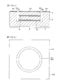
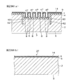
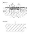
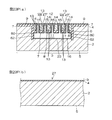
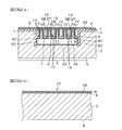
- FIG. 1 is a schematic plan view of a silicon substrate used in the manufacturing process of a pressure sensor according to an embodiment of the present invention.
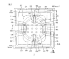
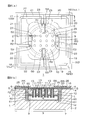
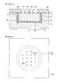
- FIG. 2 is an enlarged plan view of the pressure sensor according to the first embodiment.
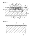
- 3A is a cross-sectional view taken along the section line AA of FIG. 2
- FIG. 3B is a cross-sectional view of the main part of the pressure sensor in the integrated circuit region of FIG.
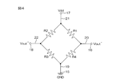
- FIG. 4 is a circuit diagram of a bridge circuit composed of metal wiring and piezoresistors.
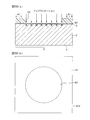
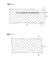
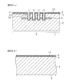
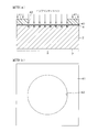
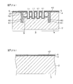
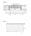
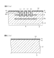
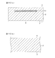
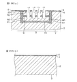
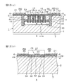
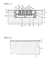
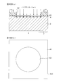
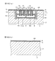
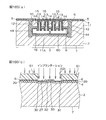
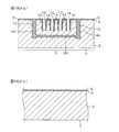
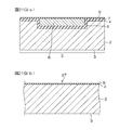
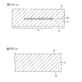
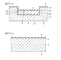
- FIG. 5A (a) is a schematic cross-sectional view showing a manufacturing process of the pressure sensor shown in FIGS. 2 and 3, and shows a cut surface at the same position as FIG. 3 (a).
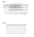
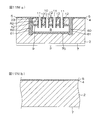
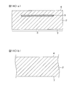
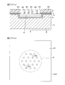
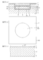
- FIG. 5B (a) is a schematic cross-sectional view showing the next step of FIG. 5A (a)
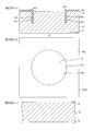
- FIG. 5B (b) is a plan view in the state of FIG. 5B (a)
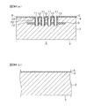
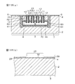
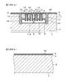
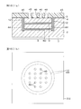
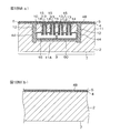
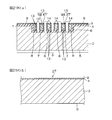
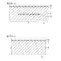
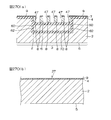
- FIG. 5C (a) is a schematic cross-sectional view showing the next step of FIG. 5B (a)
- FIG. 5C (b) is the same as FIG. 3 (b) at the same time as FIG. 5C (a).
- the cut surface at the position is shown.
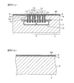
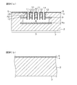
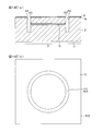
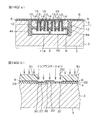
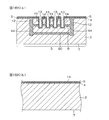
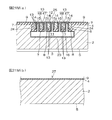
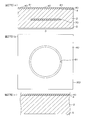
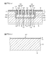
- 5D (a) is a schematic cross-sectional view showing the next step of FIG. 5C (a)
- FIG. 5D (b) is a plan view in the state of FIG.
- FIG. 5D (a), and FIG. ) Shows the cut surface at the same position as FIG. 3B at the same time as FIG. 5D (a).
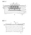
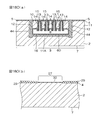
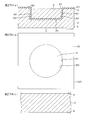
- FIG. 5E (a) is a schematic cross-sectional view showing the next step of FIG. 5D (a)
- FIG. 5E (b) is a plan view in the state of FIG. 5E (a).
- FIG. 5F (a) is a schematic cross-sectional view showing the next step of FIG. 5E (a)
- FIG. 5F (b) is the same as FIG. 3 (b) at the same time as FIG. 5F (a).
- the cut surface at the position is shown.
- FIG. 5G (a) is a schematic cross-sectional view showing the next step of FIG. 5F (a), and FIG.
- FIG. 5G (b) is the same as FIG. 3 (b) at the same time as FIG. 5G (a).
- the cut surface at the position is shown.
- FIG. 5H (a) is a schematic cross-sectional view showing the next step of FIG. 5G (a)
- FIG. 5H (b) is the same as FIG. 3 (b) at the same time as FIG. 5H (a).
- the cut surface at the position is shown.
- FIG. 5I (a) is a schematic cross-sectional view showing the next step of FIG. 5H (a)
- FIG. 5I (b) is the same as FIG. 3 (b) at the same time as FIG. 5I (a).
- the cut surface at the position is shown.
- 5J (a) is a schematic cross-sectional view showing the next step of FIG. 5I (a), and FIG. 5J (b) is the same as FIG. 3 (b) at the same time as FIG. 5J (a).
- the cut surface at the position is shown.
- 5K (a) is a schematic cross-sectional view showing the next step of FIG. 5J (a), and FIG. 5K (b) is the same as FIG. 3 (b) at the same time as FIG. 5K (a).
- the cut surface at the position is shown.
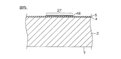
- FIG. 5L is a schematic cross-sectional view showing a step subsequent to FIG. 5K (b).
- FIG. 5M (a) is a schematic cross-sectional view at the same position as FIG. 3 (a), showing the next step of FIG.
- FIG. 5N is a schematic cross-sectional view showing a step subsequent to FIG. 5M (b).
- FIG. 5O (a) is a schematic cross-sectional view at the same position as FIG. 3 (a), showing the next step of FIG. 5N, and FIG. 5O (b) is the same time point as FIG. 5O (a).
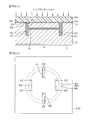
- FIG. 6A is an enlarged plan view of the pressure sensor according to the second embodiment, and FIG. 6B is a cross-sectional view taken along the section line BB in FIG. 6A.
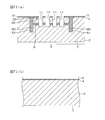
- FIG. 7A (a) is a schematic cross-sectional view showing the manufacturing process of the pressure sensor shown in FIG. 6, showing a cut surface at the same position as FIG. 6 (b), and FIG. It is principal part sectional drawing of the pressure sensor in the integrated circuit area
- FIG. 7B (a) is a schematic cross-sectional view showing the next step of FIG. 7A (a)
- FIG. 7B (b) is a plan view in the state of FIG. 7B (a).
- FIG. 7C (a) is a schematic cross-sectional view showing the next step of FIG. 7B (a), and FIG. 7C (b) is the same as FIG. 7A (b) at the same time as FIG.
- FIG. 7D (a) is a schematic cross-sectional view showing the next step of FIG. 7C (a)
- FIG. 7D (b) is a plan view in the state of FIG. 7D (a)
- FIG. ) Shows a cut surface at the same position as FIG. 7A (b) at the same time as FIG. 7D (a).
- FIG. 7E (a) is a schematic cross-sectional view showing the next step of FIG. 7D (a)
- FIG. 7E (b) is a plan view in the state of FIG. 7E (a).
- FIG. 7F is a schematic cross-sectional view showing a step subsequent to FIG. 7E (a).
- FIG. 7G (a) is a schematic cross-sectional view showing the next step of FIG. 7F
- FIG. 7G (b) is a plan view in the state of FIG. 7G (a).
- FIG. 7H (a) is a schematic cross-sectional view showing the next step of FIG. 7G (a)
- FIG. 7H (b) is a plan view in the state of FIG. 7H (a).
- FIG. 7I (a) is a schematic cross-sectional view showing the next step of FIG. 7H (a)
- FIG. 7I (b) is the same as FIG. 7A (b) at the same time as FIG. 7I (a). The cut surface at the position is shown.
- FIG. 7J (a) is a schematic cross-sectional view showing the next step of FIG.
- FIG. 7I (a), and FIG. 7J (b) is the same as FIG. 7A (b) at the same time as FIG. 7J (a).
- the cut surface at the position is shown.
- FIG. 7K (a) is a schematic cross-sectional view showing the next step of FIG. 7J (a)
- FIG. 7K (b) is the same as FIG. 7A (b) at the same time as FIG. 7K (a).
- the cut surface at the position is shown.
- 7L (a) is a schematic cross-sectional view showing the next step of FIG. 7K (a)
- FIG. 7L (b) is the same as FIG. 7A (b) at the same time as FIG. 7L (a).
- the cut surface at the position is shown.
- FIG. 7K (a) is a schematic cross-sectional view showing the next step of FIG. 7K (a)
- FIG. 7L (b) is the same as FIG. 7A (b) at the same time as FIG. 7L (a
- FIG. 7M (a) is a schematic cross-sectional view showing the next step of FIG. 7L (a), and FIG. 7M (b) is the same as FIG. 7A (b) at the same time as FIG. 7M (a).
- the cut surface at the position is shown.
- FIG. 7N (a) is a schematic cross-sectional view showing the next step of FIG. 7M (a), and FIG. 7N (b) is the same as FIG. 7A (b) at the same time as FIG. 7N (a).
- FIG. 7O is a schematic cross-sectional view showing a step subsequent to FIG. 7N (b).
- FIG. 7P (a) is a schematic cross-sectional view at the same position as FIG.
- FIG. 7Q is a schematic cross-sectional view showing a step subsequent to FIG. 7P (b).
- 7R (a) is a schematic cross-sectional view at the same position as FIG. 6 (b), showing the next step of FIG. 7Q, and FIG. 7R (b) is the same time point as FIG. 7R (a).
- the cut surface in the same position as FIG. 7A (b) is shown.
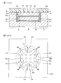
- FIG. 8A is an enlarged plan view of the pressure sensor according to the third embodiment, and FIG.
- FIG. 8B is a cross-sectional view taken along the section line CC in FIG. 8A.
- FIG. 9A (a) is a schematic cross-sectional view showing the manufacturing process of the pressure sensor shown in FIG. 8, showing a cut surface at the same position as FIG. 8 (b), and FIG. It is principal part sectional drawing of the pressure sensor in the integrated circuit area
- FIG. 9B (a) is a schematic cross-sectional view showing the next step of FIG. 9A (a), and FIG. 9B (b) is a plan view in the state of FIG. 9B (a).
- 9C (a) is a schematic cross-sectional view showing the next step of FIG. 9B (a), and FIG.
- FIG. 9C (b) is the same as FIG. 9A (b) at the same time as FIG. 9C (a).
- the cut surface at the position is shown.
- FIG. 9D is a schematic cross-sectional view showing the next step of FIG. 9C (a).
- FIG. 9E is a schematic cross-sectional view showing a step subsequent to FIG. 9D.
- 9F (a) is a schematic cross-sectional view showing the next step of FIG. 9E
- FIG. 9F (b) is a plan view in the state of FIG. 9F (a)
- FIG. 9F (c) 9C shows a cut surface at the same position as FIG. 9A (b) at the same time as FIG. 9F (a).
- FIG. 9D is a schematic cross-sectional view showing the next step of FIG. 9C (a).
- FIG. 9E is a schematic cross-sectional view showing a step subsequent to FIG. 9D.
- 9F (a) is a schematic cross-sectional view showing
- 9G (a) is a schematic cross-sectional view showing the next step of FIG. 9F (a), and FIG. 9G (b) is a plan view in the state of FIG. 9G (a).
- 9H (a) is a schematic cross-sectional view showing the next step of FIG. 9G (a), and FIG. 9H (b) is the same as FIG. 9A (b) at the same time as FIG. 9H (a).
- the cut surface at the position is shown.
- 9I (a) is a schematic cross-sectional view showing the next step of FIG. 9H (a)
- FIG. 9I (b) is the same as FIG. 9A (b) at the same time as FIG. 9I (a).
- the cut surface at the position is shown.
- 9J (a) is a schematic cross-sectional view showing the next step of FIG. 9I (a), and FIG. 9J (b) is the same as FIG. 9A (b) at the same time as FIG. 9J (a).
- the cut surface at the position is shown.
- 9K (a) is a schematic cross-sectional view showing the next step of FIG. 9J (a), and FIG. 9K (b) is the same as FIG. 9A (b) at the same time as FIG. 9K (a).
- the cut surface at the position is shown.
- 9L (a) is a schematic cross-sectional view showing the next step of FIG. 9K (a), and FIG. 9L (b) is the same as FIG. 9A (b) at the same time as FIG. 9L (a).
- FIG. 9M (a) is a schematic cross-sectional view showing the next step of FIG. 9L (a), and FIG. 9M (b) is the same as FIG. 9A (b) at the same time as FIG. 9M (a).
- FIG. 9N is a schematic cross-sectional view showing a step subsequent to FIG. 9M (b).
- FIG. 9O (a) is a schematic cross-sectional view at the same position as FIG. 8 (b), showing the next step of FIG. 9N, and FIG. 9O (b) is the same time point as FIG. 9O (a).
- FIG. 9B shows a cut surface at the same position as FIG. 9A (b).
- FIG. 9P is a schematic cross-sectional view showing a step subsequent to FIG. 9O (b).
- FIG. 9Q (a) is a schematic cross-sectional view at the same position as FIG. 8 (b) showing the next step of FIG. 9P, and
- FIG. 9Q (b) is the same time point as FIG. 9Q (a).
- FIG. 9B shows a cut surface at the same position as FIG. 9A (b).
- FIG. 10A is an enlarged plan view of a pressure sensor according to the fourth embodiment, and FIG. 10B is a cross-sectional view taken along a section line DD in FIG. 10A.
- FIG. 11A (a) is a schematic cross-sectional view showing the manufacturing process of the pressure sensor shown in FIG. 10, showing a cut surface at the same position as FIG.
- FIG. 11B (a) is a schematic cross-sectional view showing the next step of FIG. 11A (a), and FIG. 11B (b) is a plan view in the state of FIG. 11B (a).
- 11C (a) is a schematic cross-sectional view showing the next step of FIG. 11B (a), and FIG. 11C (b) is the same as FIG. 11A (b) at the same time as FIG. 11C (a). The cut surface at the position is shown.
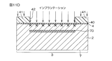
- FIG. 11D is a schematic cross-sectional view showing a step subsequent to FIG. 11C (a).
- FIG. 11E is a schematic cross-sectional view showing a step subsequent to FIG. 11D.
- 11F (a) is a schematic cross-sectional view showing the next step of FIG. 11E
- FIG. 11F (b) is a plan view in the state of FIG. 11F (a)
- FIG. 11F (c) FIG. 11B shows a cut surface at the same position as FIG. 11A (b) at the same time as FIG. 11F (a).
- FIG. 11G (a) is a schematic cross-sectional view showing the next step of FIG. 11F (a)
- FIG. 11G (b) is a plan view in the state of FIG. 11G (a).
- FIG. 11H is a schematic cross-sectional view showing a step subsequent to FIG. 11G (a).
- FIG. 11H is a schematic cross-sectional view showing a step subsequent to FIG. 11G (a).
- FIG. 11I (a) is a schematic cross-sectional view showing the next step of FIG. 11H
- FIG. 11I (b) is a plan view in the state of FIG. 11I (a).
- FIG. 11J (a) is a schematic cross-sectional view showing the next step of FIG. 11I (a)
- FIG. 11J (b) is a plan view in the state of FIG. 11J (a).
- FIG. 11K (a) is a schematic cross-sectional view showing the next step of FIG. 11J (a)
- FIG. 11K (b) is the same as FIG. 11A (b) at the same time as FIG. 11K (a).
- the cut surface at the position is shown.
- 11L (a) is a schematic cross-sectional view showing the next step of FIG.
- FIG. 11K (a), and FIG. 11L (b) is the same as FIG. 11A (b) at the same time as FIG. 11L (a).
- the cut surface at the position is shown.
- 11M (a) is a schematic cross-sectional view showing the next step of FIG. 11L (a), and FIG. 11M (b) is the same as FIG. 11A (b) at the same time as FIG. 11M (a).
- the cut surface at the position is shown.
- 11N (a) is a schematic cross-sectional view showing the next step of FIG. 11M (a), and FIG. 11N (b) is the same as FIG. 11A (b) at the same time as FIG. 11N (a).
- the cut surface at the position is shown.
- FIG. 11O (a) is a schematic cross-sectional view showing the next step of FIG. 11N (a), and FIG. 11O (b) is the same as FIG. 11A (b) at the same time as FIG. 11O (a).
- the cut surface at the position is shown.
- 11P (a) is a schematic cross-sectional view showing the next step of FIG. 11O (a), and FIG. 11P (b) is the same as FIG. 11A (b) at the same time as FIG. 11P (a).
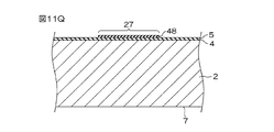
- FIG. 11Q is a schematic cross-sectional view showing a step subsequent to FIG. 11P (b).
- FIG. 11R (a) is a schematic cross-sectional view at the same position as FIG. 10 (b), showing the next step of FIG.
- FIG. 11Q, and FIG. 11R (b) is the same time as FIG. 11R (a).
- FIG. 11B shows a cut surface at the same position as FIG. 11A (b).
- FIG. 11S is a schematic cross-sectional view showing a step subsequent to FIG. 11R (b).
- 11T (a) is a schematic cross-sectional view at the same position as FIG. 10 (b), showing the next step of FIG. 11S, and FIG. 11T (b) is at the same time as FIG. 11T (a).
- FIG. 11B shows a cut surface at the same position as FIG. 11A (b).
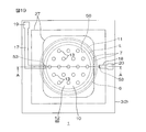
- FIG. 12 is an enlarged plan view of a pressure sensor according to the fifth embodiment.
- 13A is a cross-sectional view taken along the section line AA of FIG.
- FIG. 14A (a) is a schematic cross-sectional view showing the manufacturing process of the pressure sensor of the fifth embodiment, showing a cut surface at the same position as FIG. 13 (a), and FIG. 14A (b)
- FIG. 14B shows a cut surface at the same position as FIG. 13B at the same time as FIG. 14A (a).
- FIG. 14B (a) is a schematic cross-sectional view showing the next step of FIG. 14A (a)
- FIG. 14B (b) is a plan view in the state of FIG. 14B (a).
- 14C (a) is a schematic cross-sectional view showing the next step of FIG.
- FIG. 14B (a), and FIG. 14C (b) is the same as FIG. 13 (b) at the same time as FIG. 14C (a).
- the cut surface at the position is shown.
- 14D (a) is a schematic cross-sectional view showing the next step of FIG. 14C (a)
- FIG. 14D (b) is a plan view in the state of FIG. 14D (a)
- FIG. ) Shows a cut surface at the same position as FIG. 13B at the same time as FIG. 14D (a).
- FIG. 14E (a) is a schematic cross-sectional view showing the next step of FIG. 14D (a)
- FIG. 14E (b) is a plan view in the state of FIG. 14E (a).
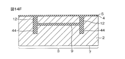
- FIG. 14F is a schematic cross-sectional view showing a step subsequent to FIG. 14E (a).
- FIG. 14G (a) is a schematic cross-sectional view showing the next step of FIG. 14F
- FIG. 14G (b) is a plan view in the state of FIG. 14G (a).
- 14H (a) is a schematic cross-sectional view showing the next step of FIG. 14G (a)
- FIG. 14H (b) is the same as FIG. 13 (b) at the same time as FIG. 14H (a).
- the cut surface at the position is shown.
- 14I (a) is a schematic cross-sectional view showing the next step of FIG. 14H (a)
- FIG. 14I (b) is the same as FIG. 13 (b) at the same time as FIG.
- FIG. 14J (a) is a schematic cross-sectional view showing the next step of FIG. 14I (a), and FIG. 14J (b) is the same as FIG. 13 (b) at the same time as FIG. 14J (a).
- the cut surface at the position is shown.
- 14K (a) is a schematic cross-sectional view showing the next step of FIG. 14J (a), and FIG. 14K (b) is the same as FIG. 13 (b) at the same time as FIG. 14K (a).
- the cut surface at the position is shown.
- 14L (a) is a schematic cross-sectional view showing the next step of FIG. 14K (a), and FIG. 14L (b) is the same as FIG.
- FIG. 14M (a) is a schematic cross-sectional view showing the next step of FIG. 14L (a), and FIG. 14M (b) is the same as FIG. 13 (b) at the same time as FIG. 14M (a).
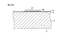
- FIG. 14N is a schematic cross-sectional view showing a step subsequent to FIG. 14M (b).
- 14A (a) shows a cut surface at the same position as FIG. 13 (a), showing the next step of FIG. 14N
- FIG. 14O (b) shows FIG. 13 at the same time as FIG. 14O (a).
- the cut surface in the same position as (b) is shown.
- FIG. 14P is a schematic cross-sectional view showing a step subsequent to FIG. 14O (b).
- FIG. 14Q (a) shows a cut surface at the same position as FIG. 13 (a), showing the next step of FIG. 14P, and
- FIG. 14Q (b) shows FIG. 13 at the same time as FIG. 14Q (a).
- the cut surface in the same position as (b) is shown.
- FIG. 15 is a cross-sectional view taken along line AA in FIG. 12 in the case of the pressure sensor of the sixth embodiment.
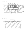
- FIG. 16A (a) is a schematic cross-sectional view showing the manufacturing process of the pressure sensor of the sixth embodiment, showing a cut surface at the same position as FIG. 15, and FIG.
- FIG. 16B (a) is a schematic cross-sectional view showing the next step of FIG. 16A (a), and FIG. 16B (b) is a plan view in the state of FIG. 16B (a).
- 16C (a) is a schematic cross-sectional view showing the next step of FIG. 16B (a), and FIG. 16C (b) is the same as FIG. 13 (b) at the same time as FIG. 16C (a).
- the cut surface at the position is shown.
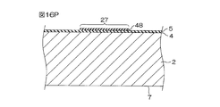
- FIG. 16D is a schematic cross-sectional view showing a step subsequent to FIG. 16C (a).
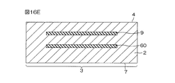
- FIG. 16E is a schematic cross-sectional view showing a step subsequent to FIG. 16D.
- FIG. 16F (a) is a schematic cross-sectional view showing the next step of FIG. 16E
- FIG. 16F (b) is a plan view in the state of FIG. 16F (a)
- FIG. 16F (c) The cut surface in the same position as FIG.13 (b) in the same time as FIG.16F (a) is shown.
- FIG. 16G (a) is a schematic cross-sectional view showing the next step of FIG. 16F (a)
- FIG. 16G (b) is a plan view in the state of FIG. 16G (a).
- FIG. 16H is a schematic sectional view showing a step subsequent to FIG. 16G (a).
- FIG. 16I (a) is a schematic cross-sectional view showing the next step of FIG. 16H, and FIG.
- 16I (b) is a plan view in the state of FIG. 16I (a).
- 16J (a) is a schematic cross-sectional view showing the next step of FIG. 16I (a)
- FIG. 16J (b) is the same as FIG. 13 (b) at the same time as FIG. 16J (a).
- the cut surface at the position is shown.
- 16K (a) is a schematic cross-sectional view showing the next step of FIG. 16J (a)
- FIG. 16K (b) is the same as FIG. 13 (b) at the same time as FIG. 16K (a).
- the cut surface at the position is shown.
- 16L (a) is a schematic cross-sectional view showing the next step of FIG. 16K (a)
- FIG. 16L (b) is the same as FIG.
- FIG. 16M (a) is a schematic cross-sectional view showing the next step of FIG. 16L (a), and FIG. 16M (b) is the same as FIG. 13 (b) at the same time as FIG. 16M (a).
- the cut surface at the position is shown.
- 16N (a) is a schematic cross-sectional view showing the next step of FIG. 16M (a), and FIG. 16N (b) is the same as FIG. 13 (b) at the same time as FIG. 16N (a).
- FIG. 16O (a) is a schematic cross-sectional view showing the next step of FIG. 16N (a), and FIG.
- FIG. 16O (b) is the same as FIG. 13 (b) at the same time as FIG. 16O (a).
- the cut surface at the position is shown.
- FIG. 16P is a schematic cross-sectional view showing a step subsequent to FIG. 16O (b).
- FIG. 16Q (a) shows a cut surface at the same position as FIG. 15 showing the next step of FIG. 16P
- FIG. 16Q (b) shows FIG. 13 (b) at the same time as FIG. 16Q (a).
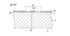
- FIG. 16R is a schematic cross-sectional view showing a step subsequent to FIG. 16Q (b).
- FIG. 16S (a) shows a cut surface at the same position as FIG. 15 showing the next step of FIG. 16R, and FIG.
- FIG. 16S (b) shows FIG. 13 (b) at the same time as FIG. 16S (a).
- the cut surface at the same position is shown.
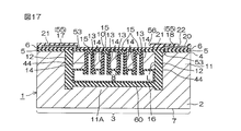
- FIG. 17 is a cross-sectional view taken along line AA in FIG. 12 in the case of the pressure sensor of the seventh embodiment.
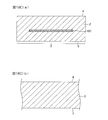
- 18A (a) is a schematic cross-sectional view showing the manufacturing process of the pressure sensor of the seventh embodiment, showing a cut surface at the same position as FIG. 17, and
- FIG. 18A (b) is a cross-sectional view of FIG.
- the cut surface in the same position as FIG.13 (b) in the same time as (a) is shown.
- FIG. 18B (a) is a schematic cross-sectional view showing the next step of FIG. 18A (a), and FIG.
- 18B (b) is a plan view in the state of FIG. 18B (a).
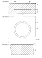
- 18C (a) is a schematic cross-sectional view showing the next step of FIG. 18B (a)
- FIG. 18C (b) is the same as FIG. 13 (b) at the same time as FIG. 18C (a).
- the cut surface at the position is shown.
- 18D (a) is a schematic cross-sectional view showing the next step of FIG. 18C (a)
- FIG. 18D (b) is a plan view in the state of FIG. 18D (a)
- FIG. ) Shows a cut surface at the same position as FIG. 13B at the same time point as FIG. 8D (a).
- FIG. 18E (a) is a schematic cross-sectional view showing the next step of FIG.
- FIG. 18D (a), and FIG. 18E (b) is a plan view in the state of FIG. 18E (a).
- FIG. 18F is a schematic cross-sectional view showing a step subsequent to FIG. 18E (a).
- FIG. 18G (a) is a schematic cross-sectional view showing the next step of FIG. 18F
- FIG. 18G (b) is a plan view in the state of FIG. 18G (a).
- 18H (a) is a schematic cross-sectional view showing the next step of FIG. 18G (a)
- FIG. 18H (b) is the same as FIG. 13 (b) at the same time as FIG. 18H (a).
- the cut surface at the position is shown.
- 18I (a) is a schematic cross-sectional view showing the next step of FIG.
- FIG. 18H (a), and FIG. 18I (b) is the same as FIG. 13 (b) at the same time as FIG. 18I (a).
- the cut surface at the position is shown.
- 18J (a) is a schematic cross-sectional view showing the next step of FIG. 18I (a), and FIG. 18J (b) is the same as FIG. 13 (b) at the same time as FIG. 18J (a).
- the cut surface at the position is shown.
- FIG. 18K (a) is a schematic cross-sectional view showing the next step of FIG. 18J (a), and FIG. 18K (b) is the same as FIG. 13 (b) at the same time as FIG. 18K (a).
- the cut surface at the position is shown.
- 18L (a) is a schematic cross-sectional view showing the next step of FIG. 18K (a), and FIG. 18L (b) is the same as FIG. 13 (b) at the same time as FIG. 18L (a).
- the cut surface at the position is shown.
- 18M (a) is a schematic cross-sectional view showing the next step of FIG. 18L (a), and FIG. 18M (b) is the same as FIG. 13 (b) at the same time as FIG. 18M (a).
- the cut surface at the position is shown.
- FIG. 18N is a schematic cross-sectional view showing a step subsequent to FIG. 18M (b).
- FIG. 18O (a) shows a cut surface at the same position as FIG. 17 showing the next step of FIG. 18N, and FIG.
- FIG. 18O (b) shows FIG. 13 (b) at the same time as FIG. 18O (a).
- the cut surface at the same position is shown.
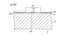
- FIG. 18P is a schematic cross-sectional view showing a step subsequent to FIG. 18O (b).
- FIG. 18Q (a) shows a cut surface at the same position as FIG. 17 showing the next step of FIG. 18P
- FIG. 18Q (b) shows FIG. 13 (b) at the same time as FIG. 18Q (a).
- FIG. 19 is an enlarged plan view of a pressure sensor according to the eighth embodiment.
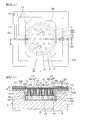
- 20A is a cross-sectional view taken along the section line AA of FIG. 19, and FIG.
- FIG. 20B is a cross-sectional view of the main part of the pressure sensor in the integrated circuit region of FIG.
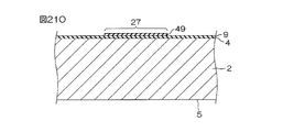
- FIG. 21A (a) is a schematic cross-sectional view showing the manufacturing process of the pressure sensor of the eighth embodiment, showing a cut surface at the same position as FIG. 20 (a), and FIG. The cut surface in the same position as FIG.20 (b) in the same time as FIG.21A (a) is shown.
- FIG. 21B (a) is a schematic cross-sectional view showing the next step of FIG. 21A (a)
- FIG. 21B (b) is a plan view in the state of FIG. 21B (a)
- FIG. ) Shows a cut surface at the same position as FIG. 20B at the same time as FIG. 21B (a).
- FIG. 21A (a) is a schematic cross-sectional view showing the manufacturing process of the pressure sensor of the eighth embodiment, showing a cut surface at the same position as FIG. 20 (a), and FIG. The cut surface in the same position as FIG
- FIG. 21C is a schematic cross-sectional view showing a step subsequent to FIG. 21B (a).
- FIG. 21D (a) is a schematic cross-sectional view showing the next step of FIG. 21C
- FIG. 21D (b) is the same position as FIG. 20 (b) at the same time as FIG. 21D (a).
- the cut surface is shown.
- FIG. 21E (a) is a schematic cross-sectional view showing the next step of FIG. 21D (a)
- FIG. 21E (b) is the same as FIG. 20 (b) at the same time as FIG. 21E (a).
- the cut surface at the position is shown.
- 21F (a) is a schematic cross-sectional view showing the next step of FIG. 21E (a), FIG.
- FIG. 21F (b) is a plan view in the state of FIG. 21F (a), and FIG. ) Shows a cut surface at the same position as FIG. 20B at the same time as FIG. 21F (a).
- FIG. 21G (a) is a schematic cross-sectional view showing the next step of FIG. 21F (a), and FIG. 21G (b) is the same as FIG. 20 (b) at the same time as FIG. 21G (a). The cut surface at the position is shown.
- FIG. 21H (a) is a schematic cross-sectional view showing the next step of FIG. 21G (a), and FIG. 21H (b) is a plan view in the state of FIG. 21H (a).
- FIG. 21H (a) is a schematic cross-sectional view showing the next step of FIG. 21G (a)
- FIG. 21H (b) is a plan view in the state of FIG. 21H (a).
- 21I (a) is a schematic cross-sectional view showing the next step of FIG. 21H (a), and FIG. 21I (b) is the same as FIG. 20 (b) at the same time as FIG. 21I (a).
- the cut surface at the position is shown.
- 21J (a) is a schematic cross-sectional view showing the next step of FIG. 21I (a), and FIG. 21J (b) is the same as FIG. 20 (b) at the same time as FIG. 21J (a).
- the cut surface at the position is shown.
- 21K (a) is a schematic cross-sectional view showing the next step of FIG. 21J (a), and FIG. 21K (b) is the same as FIG. 20 (b) at the same time as FIG. 21K (a).
- FIG. 21L (a) is a schematic cross-sectional view showing the next step of FIG. 21K (a), and FIG. 21L (b) is the same as FIG. 20 (b) at the same time as FIG. 21L (a).
- the cut surface at the position is shown.
- 21M (a) is a schematic cross-sectional view showing the next step of FIG. 21L (a), and FIG. 21M (b) is the same as FIG. 20 (b) at the same time as FIG. 21M (a).
- the cut surface at the position is shown.
- 21N (a) is a schematic cross-sectional view showing the next step of FIG. 21M (a), and FIG. 21N (b) is the same as FIG. 20 (b) at the same time as FIG.
- FIG. 21N (a).
- the cut surface at the position is shown.
- FIG. 21O is a schematic cross-sectional view showing a step subsequent to FIG. 21N (b).
- FIG. 21P (a) shows a cut surface at the same position as FIG. 20 (a), showing the next step of FIG. 21O
- FIG. 21P (b) is a view at the same time as FIG. 21P (a).
- the cut surface in the same position as (b) is shown.
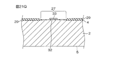
- FIG. 21Q is a schematic cross-sectional view showing a step subsequent to FIG. 21P (b).
- FIG. 21R (a) shows a cut surface at the same position as FIG. 20 (a), showing the next step of FIG. 21Q
- FIG. 21R (b) is a view at the same time as FIG.
- FIG. 22A is an enlarged plan view of the pressure sensor according to the ninth embodiment
- FIG. 22B is a cross-sectional view taken along the line BB in FIG. 22A
- FIG. 23A (a) is a schematic cross-sectional view showing the manufacturing process of the pressure sensor of the ninth embodiment, showing a cut surface at the same position as FIG. 22B, and FIG. The cut surface in the same position as FIG.20 (b) in the same time as FIG.23A (a) is shown.
- FIG. 23B (a) is a schematic cross-sectional view showing the next step of FIG. 23A (a)
- FIG. 23B (b) is a plan view in the state of FIG.
- FIG. 23B (a), and FIG. ) Shows a cut surface at the same position as FIG. 20B at the same time as FIG. 23B (a).
- FIG. 23C (a) is a schematic cross-sectional view showing the next step of FIG. 23B (a), and FIG. 23C (b) is a plan view in the state of FIG. 23C (a).
- FIG. 23D (a) is a schematic cross-sectional view showing the next step of FIG. 23C (a), and FIG. 23D (b) is the same as FIG. 20 (b) at the same time as FIG. 23D (a).
- the cut surface at the position is shown.
- FIG. 23E (a) is a schematic cross-sectional view showing the next step of FIG. 23D (a), FIG.
- FIG. 23E (b) is a plan view in the state of FIG. 23E (a), and FIG. ) Shows a cut surface at the same position as FIG. 20B at the same time as FIG.
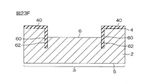
- FIG. 23F is a schematic cross-sectional view showing a step subsequent to FIG. 23E (a).
- FIG. 23G (a) is a schematic cross-sectional view showing the next step of FIG. 23F
- FIG. 23G (b) is the same position as FIG. 20 (b) at the same time as FIG. 23G (a).
- the cut surface is shown.
- FIG. 23H (a) is a schematic cross-sectional view showing the next step of FIG. 23G (a)
- FIG. 23H (b) is the same as FIG. 20 (b) at the same time as FIG.
- FIG. 23I (a) is a schematic cross-sectional view showing the next step of FIG. 23H (a)
- FIG. 23I (b) is a plan view in the state of FIG. 23I (a)
- FIG. ) Shows a cut surface at the same position as FIG. 20B at the same time as FIG.
- FIG. 23J (a) is a schematic cross-sectional view showing the next step of FIG. 23I (a)
- FIG. 23J (b) is the same as FIG. 20 (b) at the same time as FIG. 23J (a).
- FIG. 23K (a) is a schematic cross-sectional view showing the next step of FIG. 23J (a)
- FIG. 23K (a) is a schematic cross-sectional view showing the next step of FIG. 23J (a)
- 23K (b) is a plan view in the state of FIG. 23K (a).
- 23L (a) is a schematic cross-sectional view showing the next step of FIG. 23K (a)
- FIG. 23L (b) is the same as FIG. 20 (b) at the same time as FIG. 23L (a).
- the cut surface at the position is shown.
- FIG. 23M (a) is a schematic cross-sectional view showing the next step of FIG. 23L (a)
- FIG. 23M (b) is the same as FIG. 20 (b) at the same time as FIG. 23M (a).
- the cut surface at the position is shown.
- 23N (a) is a schematic cross-sectional view showing the next step of FIG. 23M (a), and FIG.
- FIG. 23N (b) is the same as FIG. 20 (b) at the same time as FIG. 23N (a).
- the cut surface at the position is shown.
- FIG. 23O (a) is a schematic cross-sectional view showing the next step of FIG. 23N (a)
- FIG. 23O (b) is the same as FIG. 20 (b) at the same time as FIG. 23O (a).
- the cut surface at the position is shown.
- FIG. 23P (a) is a schematic cross-sectional view showing the next step of FIG. 23O (a)
- FIG. 23P (b) is the same as FIG. 20 (b) at the same time as FIG. 23P (a).
- the cut surface at the position is shown.
- FIG. 23Q (a) is a schematic cross-sectional view showing the next step of FIG. 23P (a), and FIG. 23Q (b) is the same as FIG. 20 (b) at the same time as FIG. 23Q (a).
- the cut surface at the position is shown.
- FIG. 23R is a schematic cross-sectional view showing a step subsequent to FIG. 23Q (b).
- FIG. 23S (a) shows a cut surface at the same position as FIG. 22 (b), showing the next step of FIG. 23R, and FIG. 23S (b) is a view at the same time as FIG. 23S (a).
- FIG. 23T is a schematic cross-sectional view showing a step subsequent to FIG. 23S (b).
- FIG. 23U (a) shows a cut surface at the same position as FIG. 22 (b), showing the next step of FIG. 23T
- FIG. 23U (b) is a view at the same time as FIG. 23U (a).
- the cut surface in the same position as (b) is shown.
- FIG. 24A is an enlarged plan view of the pressure sensor according to the tenth embodiment
- FIG. 24B is a cross-sectional view taken along the section line CC in FIG.
- FIG. 25A (a) is a schematic cross-sectional view showing the manufacturing process of the pressure sensor of the tenth embodiment, showing a cut surface at the same position as FIG. 24 (b), FIG.
- FIG. 25A (b) The cut surface in the same position as FIG.20 (b) in the same time as FIG.25A (a) is shown.
- FIG. 25B (a) is a schematic cross-sectional view showing the next step of FIG. 25A (a)
- FIG. 25B (b) is a plan view in the state of FIG. 25B (a).
- FIG. 25C (a) is a schematic cross-sectional view showing the next step of FIG. 25B (a)
- FIG. 25C (b) is the same as FIG. 20 (b) at the same time as FIG. 25C (a).
- the cut surface at the position is shown.
- 25D (a) is a schematic cross-sectional view showing the next step of FIG. 25C (a), and FIG.
- 25D (b) is the same as FIG. 20 (b) at the same time as FIG. 25D (a).
- the cut surface at the position is shown.
- 25E (a) is a schematic cross-sectional view showing the next step of FIG. 25D (a)
- FIG. 25E (b) is a plan view in the state of FIG. 25E (a)
- FIG. ) Shows a cut surface at the same position as FIG. 20B at the same time as FIG. 25E (a).
- FIG. 25F is a schematic sectional view showing a step subsequent to FIG. 25E (a).
- FIG. 25G (a) is a schematic cross-sectional view showing the next step of FIG. 25F
- FIG. 25G (b) is the same position as FIG.
- FIG. 25H (a) is a schematic cross-sectional view showing the next step of FIG. 25G (a)
- FIG. 25H (b) is the same as FIG. 20 (b) at the same time as FIG. 25H (a).
- the cut surface at the position is shown.
- FIG. 25I (a) is a schematic cross-sectional view showing the next step of FIG. 25H (a)
- FIG. 25I (b) is a plan view in the state of FIG. 25I (a)
- FIG. ) Shows a cut surface at the same position as FIG. 20B at the same time as FIG. 25I (a).
- 25J (a) is a schematic cross-sectional view showing the next step of FIG.
- FIG. 25I (a), and FIG. 25J (b) is the same as FIG. 20 (b) at the same time as FIG. 25J (a).
- the cut surface at the position is shown.
- FIG. 25K (a) is a schematic cross-sectional view showing the next step of FIG. 25J (a)
- FIG. 25K (b) is a plan view in the state of FIG. 25K (a).
- 25L (a) is a schematic cross-sectional view showing the next step of FIG. 25K (a)
- FIG. 25L (b) is the same as FIG. 20 (b) at the same time as FIG. 25L (a).
- the cut surface at the position is shown.
- 25M (a) is a schematic cross-sectional view showing the next step of FIG. 25L (a), and FIG.
- 25M (b) is the same as FIG. 20 (b) at the same time as FIG. 25M (a).
- the cut surface at the position is shown.
- 25N (a) is a schematic cross-sectional view showing the next step of FIG. 25M (a)
- FIG. 25N (b) is the same as FIG. 20 (b) at the same time as FIG. 25N (a).
- the cut surface at the position is shown.
- FIG. 25O (a) is a schematic cross-sectional view showing the next step of FIG. 25N (a)
- FIG. 25O (b) is the same as FIG. 20 (b) at the same time as FIG. 25O (a).
- the cut surface at the position is shown.
- FIG. 25P (a) is a schematic cross-sectional view showing the next step of FIG.
- FIG. 25O (a), and FIG. 25P (b) is the same as FIG. 20 (b) at the same time as FIG. 25P (a).
- the cut surface at the position is shown.
- FIG. 25Q (a) is a schematic cross-sectional view showing the next step of FIG. 25P (a), and FIG. 25Q (b) is the same as FIG. 20 (b) at the same time as FIG. 25Q (a).
- the cut surface at the position is shown.
- FIG. 25R is a schematic sectional view showing a step subsequent to FIG. 25Q (b).
- FIG. 25S (a) shows a cut surface at the same position as FIG. 24 (b), showing the next step of FIG. 25R, and
- FIG. 25S (b) is a view at the same time as FIG. 25S (a).
- FIG. 25T is a schematic cross-sectional view showing a step subsequent to FIG. 25S (b).
- FIG. 25U (a) shows a cut surface at the same position as FIG. 24 (b), showing the next step of FIG. 25T, and
- FIG. 25U (b) is a view at the same time as FIG. 25U (a).
- FIG. 26A is an enlarged plan view of the pressure sensor according to the eleventh embodiment, and
- FIG. 26B is a cross-sectional view taken along the section line DD in FIG. FIG.
- FIG. 27A (a) is a schematic cross-sectional view showing the manufacturing process of the pressure sensor of the eleventh embodiment, showing a cut surface at the same position as FIG. 26 (b), and FIG. The cut surface in the same position as FIG.20 (b) in the same time as FIG.27A (a) is shown.
- FIG. 27B (a) is a schematic cross-sectional view showing the next step of FIG. 27A (a), and FIG. 27B (b) is a plan view in the state of FIG. 27B (a).
- 27C (a) is a schematic cross-sectional view showing the next step of FIG. 27B (a), and FIG. 27C (b) is the same as FIG. 20 (b) at the same time as FIG. 27C (a).
- FIG. 27D (a) is a schematic cross-sectional view showing the next step of FIG. 27C (a), and FIG. 27D (b) is the same as FIG. 20 (b) at the same time as FIG. 27D (a).
- the cut surface at the position is shown.
- 27E (a) is a schematic cross-sectional view showing the next step of FIG. 27D (a)
- FIG. 27E (b) is a plan view in the state of FIG. 27E (a)
- FIG. ) Shows a cut surface at the same position as FIG. 20B at the same time as FIG.
- FIG. 27F (a) is a schematic cross-sectional view showing the next step of FIG. 27E (a), and FIG.
- FIG. 27F (b) is a plan view in the state of FIG. 27F (a).
- FIG. 27G (a) is a schematic cross-sectional view showing the next step of FIG. 27F (a)
- FIG. 27G (b) is the same as FIG. 20 (b) at the same time as FIG. 27G (a).
- the cut surface at the position is shown.
- 27H (a) is a schematic cross-sectional view showing the next step of FIG. 27G (a)
- FIG. 27H (b) is a plan view in the state of FIG. 27H (a)
- FIG. ) Shows the cut surface at the same position as FIG. 20B at the same time as FIG. 27H (a).
- FIG. 27I is a schematic cross-sectional view showing a step subsequent to FIG.
- FIG. 27J (a) is a schematic cross-sectional view showing the next step of FIG. 27I
- FIG. 27J (b) is the same position as FIG. 20 (b) at the same time as FIG. 27J (a).
- the cut surface is shown.
- FIG. 27K (a) is a schematic cross-sectional view showing the next step of FIG. 27J (a)
- FIG. 27K (b) is the same as FIG. 20 (b) at the same time as FIG. 27K (a).
- the cut surface at the position is shown.
- 27L (a) is a schematic cross-sectional view showing the next step of FIG. 27K (a)
- FIG. 27L (b) is a plan view in the state of FIG. 27L (a)
- FIG. 27M (a) is a schematic cross-sectional view showing the next step of FIG. 27L (a), and FIG. 27M (b) is the same as FIG. 20 (b) at the same time as FIG. 27M (a).
- FIG. 27N (a) is a schematic cross-sectional view showing the next step of FIG. 27M (a)
- FIG. 27N (b) is a plan view in the state of FIG. 27N (a).
- 27O (a) is a schematic cross-sectional view showing the next step of FIG. 27N (a)
- FIG. 27O (b) is the same as FIG.
- FIG. 27P (a) is a schematic cross-sectional view showing the next step of FIG. 27O (a)
- FIG. 27P (b) is the same as FIG. 20 (b) at the same time as FIG. 27P (a).
- the cut surface at the position is shown.
- FIG. 27Q (a) is a schematic cross-sectional view showing the next step of FIG. 27P (a)
- FIG. 27Q (b) is the same as FIG. 20 (b) at the same time as FIG. 27Q (a).
- the cut surface at the position is shown.
- 27R (a) is a schematic cross-sectional view showing the next step of FIG. 27Q (a), and FIG.
- FIG. 27R (b) is the same as FIG. 20 (b) at the same time as FIG. 27R (a).
- the cut surface at the position is shown.
- 27S (a) is a schematic cross-sectional view showing the next step of FIG. 27R (a)
- FIG. 27S (b) is the same as FIG. 20 (b) at the same time as FIG. 27S (a).
- the cut surface at the position is shown.
- FIG. 27T (a) is a schematic cross-sectional view showing the next step of FIG. 27S (a)
- FIG. 27T (b) is the same as FIG. 20 (b) at the same time as FIG. 27T (a).
- the cut surface at the position is shown.
- FIG. 27U is a schematic cross-sectional view showing a step subsequent to FIG.
- FIG. 27V (a) shows a cut surface at the same position as FIG. 26 (b), showing the next step of FIG. 27U
- FIG. 27V (b) shows FIG. 20 at the same time as FIG. 27V (a).
- the cut surface in the same position as (b) is shown.
- FIG. 27W is a schematic cross-sectional view showing a step subsequent to FIG. 27V (b).
- FIG. 27X (a) shows a cut surface at the same position as FIG. 26 (b), showing the next step of FIG. 27W, and FIG. 27X (b) shows FIG. 20 at the same time as FIG. 27X (a).
- the cut surface in the same position as (b) is shown.
- 28A is a plan view of a circular diaphragm
- FIG. 28B is a plan view of a quadrangular diaphragm with four corners being perpendicular, and FIG. 28C is a rounded corner. It is a top view of the obtained square-shaped diaphragm.
- FIG. 29 is a graph showing the relationship between the diaphragm diameter and the sensitivity of the pressure sensor.
- FIG. 30 is a graph showing the relationship between the diaphragm thickness and the sensitivity of the pressure sensor.
- FIG. 1 is a schematic plan view of a silicon substrate used in the manufacturing process of a pressure sensor according to an embodiment of the present invention.
- the silicon substrate 2 is made of silicon that is crystal-grown while adding P-type or N-type impurities.
- the silicon substrate 2 is preferably a low resistance having a specific resistance of 5 to 100 m ⁇ ⁇ cm, for example.
- FIG. 2 is an enlarged plan view of a pressure sensor according to a first embodiment.
- 3A is a cross-sectional view taken along the section line AA of FIG. 2
- FIG. 3B is a cross-sectional view of the main part of the pressure sensor in the integrated circuit region of FIG.
- FIG. 4 is a circuit diagram of a bridge circuit composed of metal wiring and piezoresistors.
- each pressure sensor 1 includes a silicon substrate 2 having a size corresponding to the rectangular region 3.
- the surface 4 of the silicon substrate 2 is covered with a covering layer 5.
- an insulating layer 6 is formed on the surface of the covering layer 5.
- the covering layer 5 and the insulating layer 6 are both made of, for example, silicon oxide (SiO 2 ).
- the back surface 7 of the silicon substrate 2 is an exposed surface.
- a reference pressure chamber 8 is formed inside the silicon substrate 2.
- the reference pressure chamber 8 is a flat cavity (flat space) that extends parallel to the front surface 4 and the back surface 7 of the silicon substrate 2 and has a low height in the vertical direction (thickness direction of the silicon substrate 2). is there. That is, the reference pressure chamber 8 has a dimension in a direction parallel to the front surface 4 and the back surface 7 larger than a dimension in the height direction.
- One reference pressure chamber 8 is formed for each pressure sensor 1.
- the reference pressure chamber 8 is formed in a circular shape in plan view (three-dimensionally cylindrical). Inside the silicon substrate 2, an etching stop layer 9 having a circular shape in plan view that partitions the reference pressure chamber 8 from the upper side (surface 4 side) is formed. The etching stop layer 9 has a larger diameter than the reference pressure chamber 8.
- the reference pressure chamber 8 Since the reference pressure chamber 8 is formed in the silicon substrate 2, the portion facing the reference pressure chamber 8 (including the etching stop layer 9) on the surface 4 side of the silicon substrate 2 is thinner than the remaining portion.
- the silicon substrate 2 has a diaphragm 10 having a circular shape in plan view on the surface 4 side with respect to the reference pressure chamber 8.
- the diaphragm 10 is a thin film that can be displaced in the direction facing the reference pressure chamber 8 (the thickness direction of the silicon substrate 2).
- the diaphragm 10 is a part of the silicon substrate 2 and is formed on the surface layer portion of the silicon substrate 2 so as to partition the reference pressure chamber 8.
- the etching stop layer 9 is formed on the surface (lower surface) facing the reference pressure chamber 8 in the diaphragm 10, and forms a part of the diaphragm 10.
- the surface opposite to the lower surface of the diaphragm 10 is the surface 4 of the silicon substrate 2.
- the diameter of the diaphragm 10 is almost the same as the diameter of the reference pressure chamber 8, and is 200 to 600 ⁇ m in this embodiment.
- the thickness of the diaphragm 10 is, for example, 0.5 to 1 ⁇ m. However, in FIG. 3A, the thickness of the diaphragm 10 is exaggerated in order to clearly represent the structure.
- the diaphragm 10 is integrally supported by the remaining portion of the silicon substrate 2. In this embodiment, the diaphragm 10 is disposed at substantially the center of the rectangular region 3 in plan view (see FIG. 2).
- the diaphragm 10 is formed with a plurality of circular through-holes 11 in a plan view at predetermined equal intervals over the entire area inside the outline of the diaphragm 10 (in other words, the outline of the reference pressure chamber 8 in a plan view). (See FIG. 2).
- the plurality of through holes 11 are regularly arranged in a matrix along two directions intersecting in plan view. All the through holes 11 pass through a portion (including the coating layer 5 and the etching stop layer 9) between the coating layer 5 and the reference pressure chamber 8 on the surface 4 of the silicon substrate 2, and communicate with the reference pressure chamber 8. ing.
- the diameter of each through hole 11 is 0.5 ⁇ m, for example.
- the depth of each through hole 11 is, for example, 2 to 7 ⁇ m in this embodiment.
- the inner wall surface of the through hole 11 is covered with a protective thin film 12 (side wall layer, side wall insulating layer) made of silicon oxide (SiO 2 ).
- a protective thin film 12 (side wall layer, side wall insulating layer) made of silicon oxide (SiO 2 ).
- an oxide film made of silicon oxide (SiO 2 ) formed by a CVD (Chemical Vapor Deposition) method is filled and embedded inside the protective thin film 12.
- the oxide film filler 13 epibedding material
- the reference pressure whose internal pressure is used as a reference for pressure detection.
- the chamber 8 is sealed.
- the reference pressure chamber 8 is maintained in a vacuum or a reduced pressure state (for example, 10 ⁇ 5 Torr).
- the oxide film filled in the through holes 11 forms a filler 13 that closes each through hole 11 at each upper portion of the through hole 11.
- the oxide film further forms a coating film 14 that is continuous below the filler 13.
- the coating film 14 reaches the inside of the reference pressure chamber 8 and covers the entire inner wall surface of the reference pressure chamber 8.
- each pressure sensor 1 further includes piezoresistors R1 to R4 as strain gauges, metal terminals 15 to 18, and metal wirings 19 to 22.
- Piezoresistors R1 to R4 are diffused resistors formed in the surface layer portion (around the surface 4) of the silicon substrate 2 by introducing impurities such as boron (B) into the silicon substrate 2, and are also referred to as “gauges”.
- the four piezoresistors R 1 to R 4 are arranged at substantially equal intervals along the circumferential direction of the substantially circular diaphragm 10.
- the pair of piezoresistors R1 and R3 facing each other across the center of the diaphragm 10 is a rod extending along the radial direction of the circular contour L of the diaphragm 10, and is formed so as to straddle the inside and outside of the diaphragm 10 in plan view.
- the other pair of piezoresistors R2 and R4 facing each other across the center of the diaphragm 10 has a rod shape extending along the tangential direction with respect to the contour L of the diaphragm 10, and is formed so as to be accommodated inside the diaphragm 10 in plan view. ing.
- Relay wires 23 are connected to both ends of each of the piezoresistors R1 to R4.
- the relay wiring 23 is also formed in the surface layer portion of the silicon substrate 2 by introducing impurities into the silicon substrate 2 in the same manner as the piezoresistors R1 to R4.
- the relay wiring 23 is, for example, a P + region formed by introducing a high concentration of P-type impurities, and extends from the connected piezoresistor to the outside of the contour L of the diaphragm 10.
- the metal terminals 15 to 18 include a ground terminal 15 (GND), a negative side voltage output terminal 16 (Vout ⁇ ), a voltage application terminal 17 (Vdd), and a positive side voltage output terminal 18 (Vout + ). It is out. These four metal terminals 15 to 18 are formed on the insulating layer 6 (see FIG. 3A), and are arranged one by one at the four corners of the rectangular region 3.
- the metal terminals 15 to 18 are made of aluminum (Al) in this embodiment.
- the metal wirings 19 to 22 are wirings for forming a bridge circuit (Wheatstone bridge) shown in FIG. 4 by bridge-connecting the piezoresistors R1 to R4.
- the metal wiring 19 is a grounding wiring 19 that connects the piezoresistor R 3 and the piezoresistor R 4 outside the diaphragm 10 and is connected to the ground terminal 15.
- the metal wiring 20 is a negative output wiring 20 that connects the piezoresistor R1 and the piezoresistor R4 outside the diaphragm 10 and is connected to the negative voltage output terminal 16.
- the metal wiring 21 is a voltage application wiring 21 that connects the piezoresistor R1 and the piezoresistance R2 outside the diaphragm 10 and is connected to the voltage application terminal 17.
- the metal wiring 22 is a positive output wiring 22 that connects the piezoresistor R 2 and the piezoresistor R 3 outside the diaphragm 10 and is connected to the positive voltage output terminal 18.
- these metal wirings 19 to 22 are made of aluminum (Al) and are formed on the insulating layer 6 (see FIG. 3A).
- Each of the metal wirings 19 to 22 extends linearly from the corresponding piezoresistor along the radial direction of the diaphragm 10, bends at a substantially right angle in the vicinity of the outer peripheral edge of the rectangular region 3, and forms the outer peripheral edge of the rectangular region 3. It extends in a straight line along and is connected to a corresponding metal terminal.
- the metal wirings 19 to 22 and the piezo resistors R1 to R4 are relayed by the relay wiring 23.
- the metal terminals 15 to 18 (metal terminal 16 in FIG. 3A) and the metal wirings 19 to 22 (metal wirings 20 and 21 in FIG. 3A) are nitrided. It is covered with a passivation film 25 made of silicon (SiN). In the passivation film 25, openings 26 for exposing the metal terminals 15 to 18 as pads are formed. In FIG. 2, illustration of the passivation film 25 is omitted.
- the diaphragm 10 receives pressure (for example, gas pressure) from the surface 4 side of the silicon substrate 2, a differential pressure is generated between the inside and the outside of the reference pressure chamber 8, so that the diaphragm 10 is made of silicon. It is displaced in the thickness direction of the substrate 2. Due to the displacement, the silicon crystals constituting the piezo resistors R1 to R4 are distorted, and the resistance values of the piezo resistors R1 to R4 are changed.
- pressure for example, gas pressure
- the voltage between the output terminals 16 and 18 changes according to changes in the resistance values of the piezoresistors R1 to R4. Therefore, the magnitude of the pressure generated in the pressure sensor 1 can be detected based on the voltage change.
- the outer peripheral edge specifically, the portion extending linearly along the outer peripheral edge of rectangular region 3 in each of metal wirings 19 to 22
- An integrated circuit area 27 (area surrounded by a two-dot chain line) is provided between the diaphragm 10 and the diaphragm 10.
- the integrated circuit region 27 is a substantially rectangular annular region surrounding the diaphragm 10 in plan view.
- the pressure sensor 1 includes an integrated circuit portion 28 formed on the silicon substrate 2 on which the diaphragm 10 and the like are formed.
- the integrated circuit region 27 is insulated and isolated from other regions of the silicon substrate 2 by the LOCOS layer 29.
- a source 30 and a drain 31 are formed in the surface layer portion of the silicon substrate 2 in the integrated circuit region 27, and a gate oxide film 32 is formed in a portion corresponding to the integrated circuit region 27 on the surface 4 of the silicon substrate 2. It is formed across the source 30 and the drain 31.
- a gate electrode 33 is formed so as to face a portion between the source 30 and the drain 31 (a portion where a channel is formed).
- An insulating layer 6 is formed on the LOCOS layer 29 and the gate oxide film 32 so as to cover the gate electrode 33.
- a source-side metal wiring 35 and a drain-side metal wiring 36 are provided on the surface of the insulating layer 6.
- the source side metal wiring 35 is connected to the source 30 through the insulating layer 6 and the gate oxide film 32.
- the drain side metal wiring 36 penetrates through the insulating layer 6 and the gate oxide film 32 and is connected to the drain 31.
- a passivation film 25 is formed on the surface of the insulating layer 6 so as to cover the source-side metal wiring 35 and the drain-side metal wiring 36.
- the component group arranged in the integrated circuit region 27 is referred to as an integrated circuit unit 28.
- FIGS. 5A to 5O show a manufacturing process of the pressure sensor shown in FIGS.
- the upper cross-sectional view shows a cut surface at the same position as FIG. 3A
- the lower cross-sectional view shows FIG. The cut surface in the same position as (b) is shown.
- a silicon substrate 2 wafer
- the thickness of the silicon substrate 2 at this point is about 300 ⁇ m.
- the thickness is reduced to 300 ⁇ m.
- the state is shown in FIG. 5A.
- an oxide film 40 having a thickness of several hundreds of millimeters is formed on the surface 4 of the silicon substrate 2 by thermal oxidation or CVD.
- a resist pattern 41 is formed on the oxide film 40 by photolithography.
- the resist pattern 41 has one round opening 42 corresponding to the etching stop layer 9 (see FIG. 3A) (see FIG. 5B).
- impurities for example, nitrogen (N) ions or oxygen (O) ions
- the acceleration voltage at the time of ion implantation may be about 50 to 120 keV, for example.
- the oxide film 40 suppresses damage to the surface 4 caused by ion implantation.
- a process of epitaxially growing a semiconductor layer on the surface 4 of the silicon substrate 2 is performed. Since the silicon substrate 2 is heated during the epitaxial growth, the impurity ions implanted into the silicon substrate 2 are activated. Thereby, as shown in FIG. 5C (a), an etching stop layer 9 made of silicon oxide (SiO 2 ) or silicon nitride (SiN) is formed at a predetermined depth from the surface 4 of the silicon substrate 2. .
- the portion above the etching stop layer 9 (between the etching stop layer 9 and the surface 4) is an epitaxially grown silicon layer (epitaxial layer).
- the thickness of the epitaxial layer is, for example, about 0.5 to 1 ⁇ m.
- the etching stop layer 9 is placed at a predetermined depth from the surface 4 of the silicon substrate 2 (for example, 0.5 to 0.5 from the surface 4) only by heat treatment of the silicon substrate 2 (drive-in for implantation ion diffusion). To a depth of about 1 ⁇ m).
- the acceleration voltage of the implantation is increased, and the impurity ions (oxygen ions or nitrogen ions) are supplied from the surface 4 of the silicon substrate 2 to the predetermined value.
- the acceleration voltage of impurity ions is, for example, about 200 to 400 keV.
- an etching stop layer 9 made of oxide or nitride is formed at a predetermined depth from the surface 4 of the silicon substrate 2. Thereafter, the oxide film 40 (see FIG. 5B (a)) is removed.
- the silicon substrate 2 can be made thinner by the absence of the epitaxial layer.
- FIG. 5D (a) an oxide film 43 having a thickness of several hundreds of millimeters is formed on the surface 4 of the silicon substrate 2 by thermal oxidation or CVD, and then the surface layer portion of the silicon substrate 2 is formed. Then, impurities (for example, boron (B)) are implanted through a mask 44 having a predetermined pattern. Subsequently, the oxide film 43 and the mask 44 are removed, and drive-in is performed. By this drive-in, ions of impurities implanted into the silicon substrate 2 are activated, and piezoresistors (gauges) R1 to R4 are formed on the surface layer portion of the silicon substrate 2 (see also FIG. 5D (b)). .
- FIG. 5D (a) shows only the piezoresistor R2 among the piezoresistors R1 to R4.
- relay wiring (P + region) 23 is formed on the silicon substrate 2 so as to be continuous with each of the piezoresistors R1 to R4 in the same procedure as that for the piezoresistors R1 to R4. That is, formation of an oxide film and a resist mask on the surface of the silicon substrate 2, implantation of P-type impurity ions (for example, boron ions), removal of the oxide film and the resist mask, and drive-in are sequentially performed. In this case, the resist mask has an opening corresponding to the pattern of the relay wiring 23.
- P-type impurity ions for example, boron ions
- a coating layer 5 made of silicon oxide (SiO 2 ) is formed on the surface 4 of the silicon substrate 2 by a CVD method.
- a resist pattern 45 is formed on the coating layer 5 by photolithography.
- the resist pattern 45 has a plurality of openings 46 corresponding to the plurality of through holes 11 (see FIGS. 2 and 3A).
- the opening 46 is formed in a circular shape accordingly.
- the diameter of each opening 46 is about 0.5 ⁇ m, similar to the through hole 11.
- each opening 46 is formed at a position that does not overlap with the piezoresistors R1 to R4 and each relay wiring 23 (see FIG. 5E (b)).
- FIG. 5E shows a state where the plasma etching is finished.
- the silicon substrate 2 is dug down by anisotropic deep RIE (Reactive Ion Etching) using the resist pattern 45 as a mask.
- the through holes 11 are formed at positions corresponding to the openings 46 of the resist pattern 45 in the silicon substrate 2 (in other words, portions selectively removed in the coating layer 5). It is formed. If the opening 46 is circular, the through-hole 11 having a cylindrical concave shape extending downward from the coating layer 5 on the surface 4 is formed. Each through hole 11 penetrates the etching stop layer 9 and is formed so that the bottom surface of each through hole 11 is located below the etching stop layer 9. When the through hole 11 is formed, the resist pattern 45 is simultaneously etched and thinned. After the through hole 11 is formed, the remaining portion of the resist pattern 45 is peeled off.
- Deep RIE for forming the through hole 11 may be performed by a so-called Bosch process.
- Bosch process the process of etching the silicon substrate 2 using SF 6 (sulfur hexafluoride) and the process of forming a protective film on the etched surface using C 4 F 8 (perfluorocyclobutane) are alternated. Repeated. Thereby, the silicon substrate 2 can be etched with a high aspect ratio.
- the entire inner surface that is, the circumferential surface and the bottom surface of the through hole 11
- the coating layer 5 that define each through hole 11 in the silicon substrate 2 by thermal oxidation or CVD.
- a protective thin film 12 made of silicon oxide (SiO 2 ) is formed on the surface.
- the thickness of the protective thin film 12 is about 1000 mm.
- the protective thin film 12 in each through hole 11 has a cylindrical shape (specifically, a cylindrical shape) that covers the sidewall of the through hole 11 and penetrates the etching stop layer 9, and is formed at the lower end of the through hole 11. It has a bottom part.
- an etching agent is introduced into each through hole 11 from the surface 4 side of the silicon substrate 2 (isotropic etching). For example, when dry etching such as plasma etching is applied, an etchant gas is introduced into the through hole 11. In addition, when wet etching is applied, an etching solution is introduced into the through hole 11.
- the substrate material around the bottom of each through hole 11 in the silicon substrate 2 (that is, below the etching stop layer 9) is equalized using the coating layer 5 and the protective thin film 12 on the inner surface of each through hole 11 as a mask.
- a reference pressure chamber 8 (flat space) communicating with each through hole 11 is formed inside the silicon substrate 2 below the etching stop layer 9 and around the bottom of each through hole 11. It is formed.
- a diaphragm 10 is formed on the etching stop layer 9.
- the depth of the completed reference pressure chamber 8 (the dimension in the thickness direction of the silicon substrate 2) is, for example, 10 to 15 ⁇ m.
- each through hole 11 is filled with an oxide film and closed by a CVD method. More specifically, an oxide film is formed on the upper portion of the inner side portion of the protective thin film 12 on the circumferential surface of the through hole 11 so as to close the through hole 11.
- This oxide film is the filler 13 described above. That is, in this step, the filler 13 is disposed in each through hole 11.
- the oxide film for closing the through-hole 11 is not limited to the inside of the through-hole 11 but reaches the inside of the reference pressure chamber 8 from the bottom of the through-hole 11 continuously as the above-described coating film 14 to the filler 13.
- the entire inner wall surface of the reference pressure chamber 8 is covered. Since the reference pressure chamber 8 has a sufficient depth (10 to 15 ⁇ m), it is not filled with the coating film 14. In addition, since the through-hole 11 is obstruct
- the integrated circuit region 27 is a region other than the region where the reference pressure chamber 8 and the diaphragm 10 are formed in the silicon substrate 2.
- a nitride film 48 made of silicon nitride (SiN) is formed on the surface of the coating layer 5 of the silicon substrate 2.
- the nitride film 48 is selectively removed by plasma etching through a mask (not shown) having a predetermined pattern. As a result, the nitride film 48 remains only in the portion that is to become the integrated circuit region 27.
- the surface portion of the surrounding silicon substrate 2 is thermally oxidized to form a LOCOS layer 29 around the nitride film 48.
- the nitride film 48 and the underlying coating layer 5 are removed, and the above-described gate oxide film 32 is newly formed by, for example, a thermal oxidation method.
- FIG. 5M (b) A region where the gate oxide film 32 is formed in the silicon substrate 2 (region separated by the LOCOS layer 29) becomes an integrated circuit region 27.
- a polysilicon film is deposited on the gate oxide film 32 in the integrated circuit region 27.
- a gate electrode 33 is formed on the gate oxide film 32 as shown in FIG. 5N.
- a resist pattern 51 is formed on the surface of the silicon substrate 2.
- the resist pattern 51 has one opening 52 corresponding to the integrated circuit region 27.
- impurities for example, arsenic (As) ions
- the source 30 and the drain 31 are formed in regions facing each other with the gate electrode 33 interposed therebetween.
- the insulating layer 6 covering the surface of the silicon substrate 2 is formed by the CVD method. Specifically, the insulating layer 6 is formed so as to cover the covering layer 5 shown in FIG. 5O (a) and the LOCOS layer 29 and the gate oxide film 32 shown in FIG. 5O (b).
- an opening (contact hole) 53 is formed so as to penetrate the insulating layer 6 and the covering layer 5 by photolithography. The opening 53 is formed at a position where a part of the relay wiring 23 continuous to the piezoresistors R1 to R4 is exposed.
- contact holes 54 for the source 30 and the drain 31 are formed.
- the contact hole 54 is formed so as to penetrate the insulating layer 6 and the gate oxide film 32 so as to expose each part of the source 30 and the drain 31. Although not shown, in the same process, a contact hole connected to the gate electrode 33 is formed so as to penetrate the insulating layer 6.
- aluminum is deposited on the insulating layer 6 by sputtering to form an aluminum deposited film 55.
- the aluminum deposited film 55 is connected to each of the piezoresistors R1 to R4, the source 30, the drain 31, and the gate electrode 33 through contact holes 53, 54, and the like.
- a resist pattern (not shown) is formed on the aluminum deposited film 55 by photolithography, and then the aluminum deposited film 55 is selectively removed by plasma etching using the resist pattern as a mask. Thereby, the metal terminals 15 to 18 and the metal wirings 19 to 22 are formed simultaneously (see FIG. 2).
- a metal wiring (such as the source-side metal wiring 35 and the drain-side metal wiring 36 described above) and a metal terminal (not shown) connected to the source 30, the drain 31 and the gate electrode 33 of the integrated circuit portion 28 are formed at the same time. The Thereafter, the resist pattern is peeled off.
- a passivation film 25 is formed on the insulating layer 6 by the CVD method. Thereafter, as shown in FIG. 3A, the openings for exposing the metal terminals 15 to 18 (including metal terminals (not shown) on the integrated circuit portion 28 side) as pads are formed in the passivation film 25 by photolithography and etching. 26 is formed.
- FIG. 3A shows an opening 26 through which the metal terminal 16 is exposed.
- region surrounding all the through-holes 11 in the insulating layer 6 is formed in the passivation film 25 by photolithography and etching.
- the opening 56 is, for example, a circular shape that is similar to the reference pressure chamber 8 in plan view.
- the pressure sensor 1 according to the first embodiment shown in FIGS. 2 and 3 is obtained.
- the reason why the opening 56 is formed in the passivation film 25 and the diaphragm 10 is exposed from the opening 56 is to make the diaphragm 10 bend easily.
- the passivation film 25 exists on the diaphragm 10 the diaphragm 10 is difficult to bend and the sensitivity of the pressure sensor 1 is lowered.
- the substrate material is etched with the etching agent introduced into the through hole 11.
- the reference pressure chamber 8 is formed under the etching stop layer 9, while the diaphragm 10 is formed over the etching stop layer 9.
- the diaphragm 10 is cut off from the etching agent introduced into the reference pressure chamber 8 by the etching stop layer 9.
- the reference pressure chamber 8 and the diaphragm 10 can be formed by a small number of processes using only one silicon substrate 2 without bonding the two silicon substrates 2.
- the cost and small (thin) pressure sensor 1 can be easily manufactured.
- the pressure sensor 1 is configured by joining two silicon substrates 2, leakage is likely to occur at the joint portion between the two silicon substrates 2.
- the diaphragm 10 which is a movable part is a part of the silicon substrate 2, the reference pressure chamber 8 can be maintained in a sealed space where no leakage occurs.
- the sensor 1 can be provided.
- the reference pressure chamber 8 under the etching stop layer 9 can be sealed by disposing the filler 13 in the through hole 11.
- the completed pressure sensor 1 can detect the pressure received by the diaphragm 10 as a relative magnitude with respect to the pressure in the reference pressure chamber 8 (reference pressure).
- the etching agent introduced into the through hole 11 in the etching process etches the side wall of the through hole 11. Can be prevented.
- the protective thin film 12 that covers the side wall of the through hole 11 and has a cylindrical shape enters the reference pressure chamber 8 from the etching stop layer 9. Protruding.
- the protective thin film 12 comes into contact with the bottom surface of the reference pressure chamber 8 and excessive deformation of the diaphragm 10 is caused. regulate. Therefore, damage to the diaphragm 10 can be prevented.
- the pressure sensor 1 and the integrated circuit portion 28 are placed on the same silicon substrate 2 (specifically, each rectangular shape in FIG. 1). Region 3) can be formed at once.
- the diaphragm 10 is configured by using a part of the silicon substrate 2, the pressure sensor 1 is formed while the surface 4 of the silicon substrate 2 is kept flat (FIG. 3A). )), And the integrated circuit portion 28 can be formed in a region other than the diaphragm 10 on the flat surface 4 of each rectangular region 3.
- the main body portion (the portion where the diaphragm 10 is formed) of the pressure sensor 1 and the integrated circuit portion 28 (LSI) can be configured by one chip (one chip) (see FIG. 2).
- the integrated circuit unit 28 may include, for example, a circuit that processes an output signal from the piezoresistor.
- FIG. 6A is an enlarged plan view of the pressure sensor according to the second embodiment
- FIG. 6B is a cross-sectional view taken along the section line BB in FIG. 6A.
- the separation layer 60 separation insulation surrounding the periphery of the diaphragm 10 is provided. Layer).
- the separation layer 60 is an annular vertical wall that partitions the diaphragm 10 in plan view (see FIG. 6A). As shown in FIG. 6B, the inner peripheral edge of the separation layer 60 and the outline of the diaphragm 10 L matches.
- the separation layer 60 extends from the coating layer 5 on the surface 4 of the silicon substrate 2 into the silicon substrate 2 to a position deeper than the bottom surface of the reference pressure chamber 8. Therefore, the separation layer 60 defines not only the diaphragm 10 but also the reference pressure chamber 8. Further, the separation layer 60 is connected to the etching stop layer 9 at a midpoint in the vertical direction (thickness direction of the silicon substrate 2). Using the etching stop layer 9 as a reference, the etching stop layer 9 is connected to the separation layer 60 so as to bisect the inside of the separation layer 60 in the vertical direction.
- the reference pressure chamber 8 exists below the diaphragm 10 (including the etching stop layer 9) in the thickness direction of the silicon substrate 2, and the separation layer 60 is provided outside the diaphragm 10 in the direction orthogonal to the thickness direction. Because it exists, the diaphragm 10 is separated from other parts of the silicon substrate 2.
- 7A to 7R show a manufacturing process of the pressure sensor shown in FIG.
- the upper cross-sectional view shows a cut surface at the same position as FIG. 6B
- the lower cross-sectional view shows The cut surface in the same position as FIG.3 (b) is shown.
- a silicon substrate 2 is prepared as shown in FIG. 7A, and an oxide film 40 is formed on the surface 4 of the silicon substrate 2 as described in FIG. 5A.
- impurity ions are implanted into the surface layer portion of the silicon substrate 2 using the resist pattern 41 as a mask.
- epitaxial growth is performed, and the etching stop layer 9 is formed at a predetermined depth from the surface 4 of the silicon substrate 2.
- the acceleration voltage for implantation is high, only drive-in may be performed instead of epitaxial growth.
- 7D an oxide film 43 is formed on the surface 4 of the silicon substrate 2, and a resist pattern (not shown) is formed on the oxide film 43 by photolithography. This resist pattern has an annular opening corresponding to the separation layer 60 (see FIG. 6).
- FIG. 7D shows a state in which the plasma etching is completed, and an annular opening 62 is formed in the oxide film 43.
- the silicon substrate 2 is dug down by anisotropic deep RIE using the oxide film 43 as a mask, and an annular trench 61 is formed in the silicon substrate 2 as shown in FIG. 7E.
- the annular trench 61 is an annular vertical groove, and the outer peripheral edge of the etching stop layer 9 is scraped over the entire circumference. Since the through hole 11 is formed in the region where the etching stop layer 9 is present (see FIG.
- the annular trench 61 surrounds the region where the through hole 11 is to be formed on the surface 4 of the silicon substrate 2. Formed. Further, the annular trench 61 is formed so as to be deeper than a portion (refer to FIG. 6B) that becomes the bottom surface of the reference pressure chamber 8 in the silicon substrate 2.
- the annular trench 61 is filled with an oxide film by the CVD method.
- the oxide film in the annular trench 61 is the separation layer 60 described above. That is, in this step, the separation layer 60 is embedded in the annular trench 61. At this time, although the oxide film protrudes from the annular trench 61, the surface of the oxide film 43 becomes uneven, but the surface of the oxide film 43 is flattened by a resist etch back method.
- Subsequent processes are the same as the processes after FIG. 5D of the first embodiment. That is, first, referring to FIG. 7G, as described with reference to FIG.
- the oxide film 43 (including the mask 44 described above) has been removed. Note that the process of forming the piezoresistors R1 to R4 and the relay wiring 23 does not have to be performed immediately after the formation of the etching stop layer 9, and may be performed at another appropriate timing in the subsequent processes.
- FIG. 7H shows a state where the plasma etching is finished.
- the silicon substrate 2 is dug down by anisotropic deep RIE using the resist pattern 45 as a mask, and as shown in FIG. 11 is formed, and the remaining portion of the resist pattern 45 is peeled off.
- the protective thin film 12 is formed on the circumferential surface and bottom surface of the through hole 11 and the surface of the coating layer 5 by thermal oxidation or CVD, as shown in FIG. 7J (a).
- the portion on the bottom surface of the through hole 11 and the portion on the surface of the coating layer 5 in the protective thin film 12 are removed by RIE.
- the filler 13 is disposed in each through hole 11 and the entire inner wall surface of the reference pressure chamber 8 is covered by the coating film 14. Covered. Next, a step of forming the integrated circuit portion 28 (see FIG. 3B) in the integrated circuit region 27 is performed.
- a nitride film 48 is formed on the surface of the coating layer 5 of the silicon substrate 2 as shown in FIG. 7N.
- the nitride film 48 remains only in a portion to be the integrated circuit region 27 by plasma etching through a mask (not shown) having a predetermined pattern. .
- the LOCOS layer 29 is formed, and then the gate oxide film 32 is formed.
- the gate electrode 33 is formed on the gate oxide film 32 as shown in FIG. 7Q.
- the source 30 and the drain 31 are formed in the surface layer portion of the silicon substrate 2 in the integrated circuit region 27, as shown in FIG. 7R (b).
- the insulating layer 6 is formed, and as described with reference to FIG. 3, the metal terminals 15 to 18 and the metal wirings 19 to 22 (see FIG. 6A) are formed simultaneously as shown in FIG.
- the metal wiring connected to each of the source 30, drain 31 and gate electrode 33 of the integrated circuit portion 28 (the source-side metal wiring 35, the drain-side metal wiring 36, etc., see FIG. 3B) and the metal terminal (Not shown) is also formed.
- a passivation film 25 is formed on the insulating layer 6, and an opening 26 and an opening 56 are formed on the passivation film 25 to expose the metal terminals 15 to 18 (including metal terminals (not shown) on the integrated circuit portion 28 side) as pads. Is formed (see FIG. 6B).
- the pressure sensor 1 of 2nd Embodiment is obtained by the above.
- the second embodiment in addition to the effects described in the first embodiment, the following effects can be achieved. That is, in the etching process (see FIGS. 7J to 7L), the diaphragm 10 and the reference pressure chamber 8 are defined by the separation layer 60 in the direction orthogonal to the thickness direction of the silicon substrate 2, so that the diaphragm 10 , It can be formed with high accuracy in the targeted dimensions. Therefore, it is possible to manufacture the pressure sensor 1 that can improve sensitivity and suppress variations in sensitivity.
- FIG. 8A is an enlarged plan view of the pressure sensor according to the third embodiment
- FIG. 8B is a cross-sectional view taken along the section line CC in FIG. 8A.
- the bottom surface of the reference pressure chamber 8 is defined as shown in FIG. 8B.
- a second etching stop layer 70 is provided at a position (position deeper than the etching stop layer 9).
- the bottom surface of the reference pressure chamber 8 is a surface facing the etching stop layer 9 from below on the inner wall surface of the reference pressure chamber 8.
- the second etching stop layer 70 has a circular shape in plan view having the same size as that of the etching stop layer 9 (hereinafter referred to as “first etching stop layer 9” for convenience of explanation).
- the first etching stop layer 9 and the second etching stop layer 70 are vertically opposed to each other with an interval corresponding to the vertical dimension (depth) of the reference pressure chamber 8.
- 9A to 9Q show manufacturing steps of the pressure sensor shown in FIG.
- the upper cross-sectional view shows a cut surface at the same position as FIG. 8B
- the lower cross-sectional view shows The cut surface in the same position as FIG.3 (b) is shown.
- a silicon substrate 2 is prepared as shown in FIG. 9A, and an oxide film 40 is formed on the surface 4 of the silicon substrate 2 as described with reference to FIG. 5A.
- impurity ions oxygen ions or nitrogen ions
- the second etching stop layer 70 is formed at a predetermined depth from the surface 4 of the silicon substrate 2.
- the position where the second etching stop layer 70 is formed is a position where the bottom surface of the reference pressure chamber 8 is to be formed in the silicon substrate 2 (for example, a depth of 10 to 17 ⁇ m from the surface 4) ( (Refer FIG.8 (b)).
- impurity ions oxygen ions
- the first etching stop layer 9 is located on the surface 4 side of the second etching stop layer 70 and at a predetermined depth (for example, 0.5 to 1 ⁇ m) from the surface 4. Is formed.
- the second etching stop layer 70 is formed if only the drive-in is performed when the first etching stop layer 9 is formed and when the second etching stop layer 70 is formed. Therefore, it is necessary to set the acceleration voltage for the implantation to be higher than the acceleration voltage for the implantation for forming the first etching stop layer 9. Then, each etching stop layer is formed in the silicon substrate 2 such that the second etching stop layer 70 is located deeper than the first etching stop layer 9.
- FIG. 9G shows a state where the plasma etching is finished.
- the silicon substrate 2 is dug down by anisotropic deep RIE using the resist pattern 45 as a mask, and penetrates through the first etching stop layer 9 as shown in FIG. 9H (a).
- the through hole 11 is formed, and the remaining portion of the resist pattern 45 is removed.
- the bottom surface of each through hole 11 is located at a depth between the first etching stop layer 9 and the second etching stop layer 70.
- the protective thin film 12 is formed on the circumferential surface and bottom surface of the through hole 11 and the surface of the coating layer 5 by thermal oxidation or CVD, as shown in FIG. 9I (a).
- FIG. 9I a
- FIG. 9J a
- the portion on the bottom surface of the through hole 11 and the portion on the surface of the coating layer 5 in the protective thin film 12 are removed by RIE.
- the first etching stop layer 9 and the second etching stop layer 70 are formed inside the silicon substrate 2 by isotropic etching.
- a reference pressure chamber 8 is formed between and around the bottom of each through hole 11.
- a diaphragm 10 is formed on the first etching stop layer 9.
- the presence of the first etching stop layer 9 does not etch the substrate material on the surface 4 side of the first etching stop layer 9, but the second etching stop layer 70 exists. Therefore, the substrate material on the back surface 7 side from the second etching stop layer 70 is not etched.
- the filler 13 is disposed in each through hole 11, and the entire inner wall surface of the reference pressure chamber 8 is covered by the coating film 14. Covered.
- a step of forming the integrated circuit portion 28 (see FIG. 3B) in the integrated circuit region 27 is performed.
- a nitride film 48 is formed on the surface of the coating layer 5 of the silicon substrate 2 as shown in FIG. 9M.
- the nitride film 48 remains only in the portion to be the integrated circuit region 27 by plasma etching through a mask (not shown) having a predetermined pattern. .
- the LOCOS layer 29 is formed, and then the gate oxide film 32 is formed.
- the gate electrode 33 is formed on the gate oxide film 32 as shown in FIG. 9P.
- the source 30 and the drain 31 are formed in the surface layer portion of the silicon substrate 2 in the integrated circuit region 27 as shown in FIG. 9Q (b).
- the insulating layer 6 is formed, and the metal terminals 15 to 18 and the metal wirings 19 to 22 (see FIG. 8A) are simultaneously formed as shown in FIG. 8 as described in FIG.
- the metal wiring connected to each of the source 30, drain 31 and gate electrode 33 of the integrated circuit portion 28 (the source-side metal wiring 35, the drain-side metal wiring 36, etc., see FIG. 3B) and the metal terminal (Not shown) is also formed.
- a passivation film 25 is formed on the insulating layer 6, and an opening 26 and an opening 56 are formed on the passivation film 25 to expose the metal terminals 15 to 18 (including metal terminals (not shown) on the integrated circuit portion 28 side) as pads. Is formed (see FIG. 8B).
- the pressure sensor 1 of 3rd Embodiment is obtained by the above.
- the third embodiment in addition to the effects described in the first embodiment, the following effects can be achieved. That is, in the etching process (FIGS. 9I to 9K), the reference pressure chamber 8 is formed by being partitioned by the first etching stop layer 9 and the second etching stop layer 70 in the thickness direction of the silicon substrate 2. Therefore, the reference pressure chamber 8 can be accurately formed with the targeted depth dimension.
- the fourth embodiment will be described.
- the same reference is made to the portions corresponding to the portions described in the first to third embodiments. Reference numerals are assigned and explanations thereof are omitted. Further, regarding the manufacturing process of the pressure sensor 1 of the fourth embodiment, detailed description of the same manufacturing processes as those described in the first to third embodiments is omitted.
- FIG. 10A is an enlarged plan view of a pressure sensor according to the fourth embodiment
- FIG. 10B is a cross-sectional view taken along a section line DD in FIG. 10A.
- the pressure sensor 1 according to the fourth embodiment in addition to the configuration of the first embodiment (see FIG. 3A), as shown in FIG. 10, the separation layer 60 of the second embodiment, The second etching stop layer 70 of the third embodiment is provided.
- the isolation layer 60 extends into the silicon substrate 2 to a position deeper than the second etching stop layer 70. Therefore, the separation layer 60 is connected to the first etching stop layer 9 at a midpoint in the vertical direction (thickness direction of the silicon substrate 2), and is also connected to the second etching stop layer 70 at the lower end thereof. ing.
- the second etching stop layer 70 is connected to the separation layer 60 so as to cover the inside of the separation layer 60 from below.
- the diaphragm 10 is separated from other parts in the silicon substrate 2.
- the reference pressure chamber 8 is partitioned in the thickness direction of the silicon substrate 2 by the first etching stop layer 9 and the second etching stop layer 70, and further in the direction perpendicular to the thickness direction, the separation layer 60. It is divided by. 11A to 11T show manufacturing steps of the pressure sensor shown in FIG.
- the upper cross-sectional view shows a cut surface at the same position as FIG. 10B
- the lower cross-sectional view shows The cut surface in the same position as FIG.3 (b) is shown.
- a silicon substrate 2 is prepared as shown in FIG. 11A, and an oxide film 40 is formed on the surface 4 of the silicon substrate 2 as described in FIG. 9A.
- impurity ions are implanted into the surface layer portion of the silicon substrate 2 using the resist pattern 41 as a mask.
- the second etching stop layer 70 is formed at a predetermined depth from the surface 4 of the silicon substrate 2.
- impurity ions are implanted again into the surface layer portion of the silicon substrate 2 using the newly provided resist pattern 41 as a mask.
- the first etching stop layer 9 is located on the surface 4 side of the second etching stop layer 70 and at a predetermined depth from the surface 4. Is formed.
- an oxide film 43 is formed on the surface 4 of the silicon substrate 2, and a resist pattern (not shown) is formed on the oxide film 43 by photolithography.
- This resist pattern has an annular opening corresponding to the separation layer 60 (see FIG. 10).
- the oxide film 43 is selectively removed by plasma etching using this resist pattern (not shown) as a mask, and an annular opening 62 is formed in the oxide film 43.
- FIG. 11F shows a state where the plasma etching is finished.
- the silicon substrate 2 is dug down by anisotropic deep RIE using the oxide film 43 as a mask, and an annular trench 61 is formed as shown in FIG. 11G (a).
- the annular trench 61 is deeper than the second etching stop layer 70, and the outer peripheral edge portions of the first etching stop layer 9 and the second etching stop layer 70 are scraped over the entire circumference.
- the annular trench 61 is completely filled with an oxide film, and the separation layer 60 is embedded in the annular trench 61. Further, as described above, the surface of the oxide film 43 is planarized by the resist etch back method. Subsequent processes are the same as the processes after FIG. 5D of the first embodiment. That is, referring to FIG. 11I, first, as described in FIG. 5D, the piezoresistors R1 to R4 and the relay wiring 23 are formed in the surface layer portion of the silicon substrate 2. When the formation of the piezoresistors R1 to R4 and the relay wiring 23 is completed, the oxide film 43 (including the mask 44 described above) has been removed. Note that the step of forming the piezoresistors R1 to R4 and the relay wiring 23 does not have to be performed immediately after the formation of the etching stop layers 9 and 70, and may be performed at other appropriate timing in the subsequent steps.
- the coating layer 5 is formed on the surface 4 of the silicon substrate 2 by the CVD method, and then the resist pattern formed on the coating layer 5 by photolithography.
- the coating layer 5 is selectively removed by plasma etching using 45 as a mask.
- FIG. 11J shows a state where the plasma etching is finished.
- the silicon substrate 2 is dug down by anisotropic deep RIE using the resist pattern 45 as a mask, and penetrates through the first etching stop layer 9 as shown in FIG. 11K (a).
- the through-hole 11 is formed, and the remaining portion of the resist pattern 45 is removed.
- the bottom surface of each through hole 11 is located at a depth between the first etching stop layer 9 and the second etching stop layer 70.
- the protective thin film 12 is formed on the circumferential surface and bottom surface of the through hole 11 and the surface of the coating layer 5 by thermal oxidation or CVD, as shown in FIG. 11L (a).
- the portion on the bottom surface of the through hole 11 and the portion on the surface of the coating layer 5 in the protective thin film 12 are removed by RIE.
- the first etching stop layer 9 and the second etching stop layer 70 are formed inside the silicon substrate 2 by isotropic etching.
- a reference pressure chamber 8 is formed between and around the bottom of each through hole 11.
- a diaphragm 10 is formed on the first etching stop layer 9.
- the presence of the first etching stop layer 9 does not etch the substrate material on the surface 4 side of the first etching stop layer 9, but the second etching stop layer 70 exists. Therefore, the substrate material on the back surface 7 side from the second etching stop layer 70 is not etched.
- the separation layer 60 exists, the substrate material outside the separation layer 60 is not etched in the direction orthogonal to the thickness direction of the silicon substrate 2.
- the filler 13 is disposed in each through-hole 11, and the entire inner wall surface of the reference pressure chamber 8 is covered by the coating film 14. Covered.
- a step of forming the integrated circuit portion 28 (see FIG. 3B) in the integrated circuit region 27 is performed.
- a nitride film 48 is formed on the surface of the coating layer 5 of the silicon substrate 2 as shown in FIG. 11P.
- the nitride film 48 remains only in a portion to be the integrated circuit region 27 by plasma etching through a mask (not shown) having a predetermined pattern. .
- the LOCOS layer 29 is formed, and then the gate oxide film 32 is formed.
- the gate electrode 33 is formed on the gate oxide film 32 as shown in FIG. 11S.
- the source 30 and the drain 31 are formed in the surface layer portion of the silicon substrate 2 in the integrated circuit region 27, as shown in FIG.
- the insulating layer 6 is formed, and the metal terminals 15 to 18 and the metal wirings 19 to 22 (see FIG. 10A) are simultaneously formed as shown in FIG. 10 as described in FIG.
- the metal wiring connected to each of the source 30, drain 31 and gate electrode 33 of the integrated circuit portion 28 (the source-side metal wiring 35, the drain-side metal wiring 36, etc., see FIG. 3B) and the metal terminal (Not shown) is also formed.
- a passivation film 25 is formed on the insulating layer 6, and an opening 26 and an opening 56 are formed on the passivation film 25 to expose the metal terminals 15 to 18 (including metal terminals (not shown) on the integrated circuit portion 28 side) as pads. Is formed (see FIG. 10B).
- FIG. 12 is an enlarged plan view of a pressure sensor according to a fifth embodiment.
- each pressure sensor 1 includes a silicon substrate 2 having a size corresponding to the rectangular region 3.
- the surface 4 of the silicon substrate 2 is covered with a covering layer 5.
- an insulating layer 6 is formed on the surface of the covering layer 5.
- the covering layer 5 and the insulating layer 6 are both made of, for example, silicon oxide (SiO 2).
- the back surface 7 of the silicon substrate 2 is an exposed surface.
- a reference pressure chamber 8 is formed inside the silicon substrate 2.
- the reference pressure chamber 8 is a flat cavity (flat space) that extends parallel to the front surface 4 and the back surface 7 of the silicon substrate 2 and has a low height in the vertical direction (thickness direction of the silicon substrate 2). is there. That is, the reference pressure chamber 8 has a dimension in a direction parallel to the front surface 4 and the back surface 7 larger than a dimension in the height direction.
- One reference pressure chamber 8 is formed for each pressure sensor 1.
- the reference pressure chamber 8 is formed in a circular shape in plan view (three-dimensionally cylindrical).
- a first etching stop layer 9 is formed as an insulating layer having a circular shape in plan view that partitions the reference pressure chamber 8 from the upper side (surface 4 side).
- the diameter of the first etching stop layer 9 is substantially the same as the diameter of the reference pressure chamber 8.
- the portion facing the reference pressure chamber 8 is made thinner than the remaining portion on the surface 4 side of the silicon substrate 2. ing.
- the silicon substrate 2 has a diaphragm 10 having a circular shape in plan view on the surface 4 side with respect to the reference pressure chamber 8.
- the diaphragm 10 is a thin film that can be displaced in the direction facing the reference pressure chamber 8 (the thickness direction of the silicon substrate 2).
- the diaphragm 10 is a part of the silicon substrate 2 and is formed in the surface layer portion of the silicon substrate 2 so as to partition the reference pressure chamber 8 from above.
- the first etching stop layer 9 is formed on the ceiling surface of the inner wall surface of the reference pressure chamber 8, which is a surface facing the reference pressure chamber 8 of the diaphragm 10, and forms a part of the diaphragm 10.
- the bottom surface faces the ceiling surface from below.
- the diameter of the diaphragm 10 is substantially the same as the diameter of the reference pressure chamber 8, and is 200 to 600 ⁇ m in this embodiment.
- the thickness of the diaphragm 10 is, for example, 0.5 to 1 ⁇ m. However, in FIG. 13A, the thickness of the diaphragm 10 is exaggerated in order to clearly represent the structure.
- Diaphragm 10 is integrally supported by another portion (referred to as remaining portion 11) in silicon substrate 2. In this embodiment, the diaphragm 10 is arrange
- an isolation insulating layer 12 surrounding the periphery of the diaphragm 10 is formed on the silicon substrate 2, an isolation insulating layer 12 surrounding the periphery of the diaphragm 10 is formed.
- the isolation insulating layer 12 is an annular vertical wall that partitions the diaphragm 10 in plan view, and the inner peripheral edge of the isolation insulating layer 12 and the contour L of the diaphragm 10 coincide (see FIG. 12).
- the isolation insulating layer 12 extends from the coating layer 5 on the surface 4 of the silicon substrate 2 into the silicon substrate 2 to a position deeper than the bottom surface of the reference pressure chamber 8.
- the isolation insulating layer 12 defines the reference pressure chamber 8 and the diaphragm 10 in a direction orthogonal to the thickness direction of the silicon substrate 2.
- the diaphragm 10 is made of silicon.
- the substrate 2 is insulated and isolated from other parts (residual part 11).
- the diaphragm 10 is formed with a large number of through-holes 13 having a circular shape in plan view at predetermined equal intervals over the entire area inside the outline L of the diaphragm 10 (in other words, the inner peripheral edge of the isolation insulating layer 12). (See FIG. 12).
- the plurality of through holes 13 are regularly arranged in a matrix along two directions that intersect in a plan view.
- All the through holes 13 pass through a portion (including the coating layer 5 and the first etching stop layer 9) between the coating layer 5 and the reference pressure chamber 8 on the surface 4 of the silicon substrate 2, and the reference pressure chamber 8. Communicating with The diameter of each through hole 13 is, for example, 0.5 ⁇ m in this embodiment. The depth of each through hole 13 is, for example, 2 to 7 ⁇ m in this embodiment.
- the inner wall surface of the through hole 13 is covered with a protective thin film 14 (side wall insulating layer) made of silicon oxide (SiO 2).
- a protective thin film 14 side wall insulating layer made of silicon oxide (SiO 2).
- an oxide film made of silicon oxide (SiO 2) formed by a CVD (Chemical Vapor Deposition) method is filled and embedded inside the protective thin film 14.
- the oxide film filling body 15 epibedding material
- the internal pressure of the reference pressure chamber 8 below the through holes 13 is used as a reference for pressure detection. Sealed as a reference pressure chamber.
- the reference pressure chamber 8 is held in a vacuum or a reduced pressure state (for example, 10-5 Torr).
- the oxide film filled in the through-holes 13 forms a filler 15 that closes each through-hole 13 at each upper portion of the through-hole 13.
- the oxide film further forms a coating film 16 that is continuous below the filler 15.
- the coating film 16 reaches the inside of the reference pressure chamber 8 and covers the entire inner wall surface of the reference pressure chamber 8.
- the first metal wiring 17 (first wiring) is connected to the diaphragm 10, and the remaining portion 11 insulated and separated from the diaphragm 10 by the isolation insulating layer 12 in the silicon substrate 2
- Metal wiring 18 (second wiring) is connected.
- the first metal wiring 17 and the second metal wiring 18 are made of aluminum (Al) in this embodiment, and are provided on the insulating layer 6.
- the first metal wiring 17 penetrates the insulating layer 6 and the covering layer 5 and is connected to the diaphragm 10.
- the second metal wiring 18 passes through the insulating layer 6 and the coating layer 5 and is connected to the remaining portion 11.
- a first metal terminal 19 is connected to the first metal wiring 17, and a second metal terminal 20 is connected to the second metal wiring 18.
- the first metal terminal 19 and the second metal terminal 20 are made of aluminum (Al) and are formed on the insulating layer 6 (see FIG. 13A).
- the first metal terminals 19 are arranged at any of the four corners of the rectangular region 3 in plan view.
- the second metal terminal 20 is disposed in the vicinity of the substantially central position in the longitudinal direction of one side of the rectangular region 3.
- the first metal wiring 17 extends linearly along the radial direction of the diaphragm 10, bends at a substantially right angle around the outer peripheral edge of the rectangular region 3, and extends linearly along the outer peripheral edge of the rectangular region 3.
- the first metal terminal 19 is connected.
- the second metal wiring 18 extends linearly along the radial direction of the diaphragm 10 and is connected to the second metal terminal 20.
- the first metal wiring 17, the second metal wiring 18, the first metal terminal 19, and the second metal terminal 20 are covered with a passivation film 21 made of silicon nitride (SiN).
- SiN silicon nitride
- the first metal terminal 19 does not appear on the cut surface of FIG.
- the passivation film 21 is formed with an opening 22 that exposes the first metal terminal 19 and the second metal terminal 20 as pads. In FIG. 12, illustration of the passivation film 21 is omitted.
- the diaphragm 10 serves as a movable electrode, and in the remaining portion 11, a capacitor structure (capacitor) is formed in which a portion facing the diaphragm 10 from below with the reference pressure chamber 8 interposed therebetween is a fixed electrode 11A.
- Diaphragm 10 and fixed electrode 11 ⁇ / b> A are insulated by isolation insulating layer 12.
- a bias voltage is applied to each of the first metal terminal 19 and the second metal terminal 20, and the potential difference between the movable electrode (diaphragm 10) and the fixed electrode 11A is constant.
- the diaphragm 10 receives pressure (for example, gas pressure) from the surface 4 side of the silicon substrate 2, a differential pressure is generated between the inside and outside of the reference pressure chamber 8, so that the diaphragm 10 is attached to the silicon substrate 2. Displaces in the thickness direction. As a result, the distance between the diaphragm 10 and the fixed electrode 11A (the depth of the reference pressure chamber 8) changes, and the capacitance between the diaphragm 10 and the fixed electrode 11A changes. Based on the change in capacitance, the magnitude of the pressure generated in the pressure sensor 1 can be detected. That is, the pressure sensor 1 is a capacitive pressure sensor.
- pressure sensor 1 is a capacitive pressure sensor.
- each rectangular region 3 of silicon substrate 2 its outer peripheral edge (specifically, a portion extending linearly along the outer peripheral edge of rectangular region 3 in first metal wiring 17) and diaphragm 10.
- an integrated circuit region 27 region surrounded by a two-dot chain line
- the integrated circuit region 27 is a substantially rectangular annular region surrounding the diaphragm 10 in plan view.
- an integrated circuit section 28 including transistors, resistors, and other integrated circuit devices (functional elements) is formed. That is, the pressure sensor 1 includes an integrated circuit portion 28 formed on the silicon substrate 2 on which the diaphragm 10 and the like are formed.
- the integrated circuit region 27 is insulated and isolated from other regions of the silicon substrate 2 by the LOCOS layer 29.
- a source 30 and a drain 31 are formed in the surface layer portion of the silicon substrate 2 in the integrated circuit region 27, and a gate oxide film 32 is formed in a portion corresponding to the integrated circuit region 27 on the surface 4 of the silicon substrate 2. It is formed across the source 30 and the drain 31.
- a gate electrode 33 is formed so as to face a portion between the source 30 and the drain 31 (a portion where a channel is formed).
- An insulating layer 6 is formed on the LOCOS layer 29 and the gate oxide film 32 so as to cover the gate electrode 33.
- a source-side metal wiring 35 and a drain-side metal wiring 36 are provided on the surface of the insulating layer 6.
- the source side metal wiring 35 is connected to the source 30 through the insulating layer 6 and the gate oxide film 32.
- the drain side metal wiring 36 penetrates through the insulating layer 6 and the gate oxide film 32 and is connected to the drain 31.
- a passivation film 21 is formed on the surface of the insulating layer 6 so as to cover the source side metal wiring 35 and the drain side metal wiring 36.
- the component group arranged in the integrated circuit region 27 is referred to as an integrated circuit unit 28.
- FIGS. 14A to 14Q show a manufacturing process of the pressure sensor of the fifth embodiment.
- the upper cross-sectional view shows a cut surface at the same position as FIG. 13A
- the lower cross-sectional view shows FIG. The cut surface in the same position as (b) is shown.
- a silicon substrate 2 wafer
- the thickness of the silicon substrate 2 at this point is about 300 ⁇ m.
- the thickness is reduced to 300 ⁇ m.
- the state is shown in FIG. 14A.
- an oxide film 40 having a thickness of several hundreds of millimeters is formed on the surface 4 of the silicon substrate 2 by thermal oxidation or CVD.
- a resist pattern 41 is formed on the oxide film 40 by photolithography.
- the resist pattern 41 has one round opening 42 corresponding to the first etching stop layer 9 (see FIG. 13A) (see FIG. 14B (b)).
- impurities for example, nitrogen (N) ions or oxygen (O) ions
- the acceleration voltage at the time of ion implantation may be about 50 to 120 keV, for example.
- the oxide film 40 suppresses damage to the surface 4 caused by ion implantation.
- the first etching stop layer 9 made of silicon oxide (SiO 2) or silicon nitride (SiN) is formed at a predetermined depth from the surface 4 of the silicon substrate 2. Is done.
- the portion above the etching stop layer 9 (between the etching stop layer 9 and the surface 4) is an epitaxially grown silicon layer (epitaxial layer).
- the thickness of the epitaxial layer is, for example, about 0.5 to 1 ⁇ m.
- the first etching stop layer 9 is placed at a predetermined depth from the surface 4 of the silicon substrate 2 (for example, from the surface 4 to 0. 0 by the heat treatment (implanted ion diffusion drive-in) of the silicon substrate 2). (Depth of about 5 to 1 ⁇ m).
- the acceleration voltage of the implantation is increased, and the impurity ions (oxygen ions or nitrogen ions) are supplied from the surface 4 of the silicon substrate 2 to the predetermined value.
- the acceleration voltage of impurity ions is, for example, about 200 to 400 keV.
- a first etching stop layer 9 made of oxide or nitride is formed at a predetermined depth from the surface 4 of the silicon substrate 2. . Thereafter, the oxide film 40 (see FIG. 14B (a)) is removed.
- the silicon substrate 2 can be made thinner by the absence of the epitaxial layer.
- a coating layer 5 made of silicon oxide (SiO 2) is formed on the surface 4 of the silicon substrate 2 by thermal oxidation or CVD, and a resist pattern (not shown) is formed on the coating layer 5 by photolithography. .
- This resist pattern has an annular opening corresponding to the isolation insulating layer 12 (see FIGS. 12 and 13A).
- the coating layer 5 is selectively removed by plasma etching using this resist pattern (not shown) as a mask.
- FIG. 14D shows a state in which the plasma etching is completed, and an annular opening 43 is formed in the coating layer 5.
- annular trench 44 is formed as shown in FIG. 14E.
- the annular trench 44 is an annular vertical groove, and the outer peripheral edge of the first etching stop layer 9 is scraped over the entire circumference. Therefore, the annular trench 44 is formed so as to surround at least a predetermined region above the first etching stop layer 9 in the silicon substrate 2. Further, the annular trench 44 is formed so as to be deeper than a portion (see FIG. 13A) that is to be the bottom surface of the reference pressure chamber 8 in the silicon substrate 2. Therefore, the annular trench 44 is formed to be deeper than the first etching stop layer 9 scheduled to be located on the ceiling surface of the reference pressure chamber 8.
- the annular trench 44 is filled with an oxide film by the CVD method.
- the oxide film in the annular trench 44 is the isolation insulating layer 12 described above. That is, in this step, the isolation insulating layer 12 is embedded in the annular trench 44. At this time, although the oxide film protrudes from the annular trench 44, the surface of the coating layer 5 becomes uneven, but the surface of the coating layer 5 is flattened by a resist etch back method.
- a resist pattern 45 is formed on the coating layer 5 by photolithography.
- the resist pattern 45 has a plurality of openings 46 corresponding to the plurality of through holes 13 (see FIGS. 12 and 13A).
- the opening 46 is formed in a circular shape accordingly.
- the diameter of each opening 46 is about 0.5 ⁇ m, similar to the through hole 13.
- all the openings 46 are formed inside the annular trench 44 (isolation insulating layer 12) (see FIG. 14G (b)).
- FIG. 14G shows a state where the plasma etching is finished.
- the silicon substrate 2 is dug down by anisotropic deep RIE using the resist pattern 45 as a mask.
- the through holes 13 are formed at positions corresponding to the openings 46 of the resist pattern 45 in the silicon substrate 2 (in other words, portions selectively removed in the coating layer 5). It is formed. If the opening 46 is circular, the through-hole 13 having a cylindrical concave shape extending downward from the coating layer 5 on the surface 4 at a predetermined depth is formed. Each through hole 13 penetrates the first etching stop layer 9 and is formed so that the bottom surface of each through hole 13 is located above (shallow position) from the bottom surface of the annular trench 44 (isolation insulating layer 12). These through holes 13 are formed in a predetermined region surrounded by the annular trench 44 (isolation insulating layer 12). When the through hole 13 is formed, the resist pattern 45 is simultaneously etched and thinned. After the through hole 13 is formed, the remaining portion of the resist pattern 45 is peeled off.
- Deep RIE for forming the through hole 13 may be performed by a so-called Bosch process.
- Bosch process the process of etching the silicon substrate 2 using SF6 (sulfur hexafluoride) and the process of forming a protective film on the etched surface using C4F8 (perfluorocyclobutane) are alternately repeated. Thereby, the silicon substrate 2 can be etched with a high aspect ratio.
- the entire inner surface that is, the circumferential surface and the bottom surface of the through-hole 13
- the coating layer 5 that define each through-hole 13 in the silicon substrate 2 by thermal oxidation or CVD.
- a protective thin film 14 made of silicon oxide (SiO 2) is formed on the surface.
- the thickness of the protective thin film 14 is about 1000 mm.
- the protective thin film 14 in each through hole 13 has a cylindrical shape (specifically, a cylindrical shape) that covers the side wall of the through hole 13 and penetrates the first etching stop layer 9. 13 has a bottom surface portion at the lower end.
- FIG. 14J (a) the portion on the bottom surface of the through-hole 13 in the protective thin film 14 (the bottom surface portion in the cylindrical protective thin film 14) and the portion on the surface of the coating layer 5 are removed by RIE. Is done. Thereby, the crystal plane of the silicon substrate 2 is exposed from the bottom surface of the through hole 13.
- an etching agent is introduced into each through-hole 13 from the surface 4 side of the silicon substrate 2. For example, when dry etching such as plasma etching is applied, an etching gas is introduced into the through hole 13. When wet etching is applied, an etching solution is introduced into the through hole 13.
- the silicon substrate 2 is under the first etching stop layer 9 (strictly, around the bottom of each through hole 13).
- the substrate material is isotropically etched. Specifically, the silicon substrate 2 is etched in the thickness direction and in the direction perpendicular to the thickness direction, starting from the bottom of each through-hole 13.
- the first etching stop layer 9 since the first etching stop layer 9 is present, the substrate material on the surface 4 side from the first etching stop layer 9 is not etched, but since the isolation insulating layer 12 is present, silicon The substrate material outside the isolation insulating layer 12 is not etched in the direction orthogonal to the thickness direction of the substrate 2.
- a reference pressure chamber 8 (flat space) communicating with each through hole 13 is formed below the first etching stop layer 9 inside the silicon substrate 2.
- a diaphragm 10 is formed above the first etching stop layer 9.
- the depth of the reference pressure chamber 8 (the dimension in the thickness direction of the silicon substrate 2) can be adjusted according to the amount of the etchant introduced.
- the depth of the reference pressure chamber 8 can be adjusted according to the interval between the adjacent through holes 13. In this case, for example, if the interval between the through holes 13 is narrow, the space that extends from the adjacent through holes 13 by etching in a relatively short time is continuously formed. Accordingly, the height of the reference pressure chamber 8 is relatively low. On the other hand, if the interval between the through holes 13 is wide, etching must be performed for a relatively long time before the spaces extending from the adjacent through holes 13 are connected. Accordingly, the height of the reference pressure chamber 8 is increased.
- the depth of the reference pressure chamber 8 By adjusting the depth of the reference pressure chamber 8 in this way, the distance between the diaphragm 10 (movable electrode) and the remaining portion 11 (fixed electrode 11A) can be controlled, and the pressure sensor 1 (see FIG. The sensitivity of a) can be adjusted.
- the isotropic etching the substrate material around the bottom of each through-hole 13 is etched.
- the portion below (bottom side) the first etching stop layer 9 in the cylindrical protective thin film 14 formed on the inner wall of each through-hole 13 is the diaphragm 10. And protrudes into the reference pressure chamber 8 and faces the bottom surface of the reference pressure chamber 8 from above at a predetermined interval. Therefore, the reference pressure chamber 8 is not completely cylindrical, and is recessed inward (downward) at the position of each through hole 13 in the top surface portion.
- each through hole 13 is filled with an oxide film and closed by the CVD method. More specifically, an oxide film is formed on the upper portion of the inner side of the protective thin film 14 on the circumferential surface of the through hole 13 so as to close the through hole 13.
- This oxide film is the filler 15 described above. That is, in this step, the filler 15 is disposed in each through hole 13.
- the reference pressure chamber 8 is sealed in a vacuum state. At this time, the oxide film protrudes from the through hole 13 to make the surface of the coating layer 5 uneven, but the surface of the coating layer 5 is flattened by a resist etch back method. The larger the through-hole 13 is, the more easily the surface of the coating layer 5 is made uneven.
- the oxide film for closing the through-hole 13 is not limited to the inside of the through-hole 13 but reaches the inside of the reference pressure chamber 8 from the bottom of the through-hole 13 continuously as the above-described coating film 16 to the filler 15.
- the entire inner wall surface of the reference pressure chamber 8 is covered. Since the reference pressure chamber 8 has a sufficient depth (for example, 10 to 15 ⁇ m), it is not filled with the coating film 16. Note that the smaller the diameter of the through hole 13, the faster the through hole 13 is closed, and thus the thinner the coating film 16.
- the integrated circuit region 27 is a region other than the region where the reference pressure chamber 8 and the diaphragm 10 are formed in the silicon substrate 2.
- a nitride film 48 made of silicon nitride (SiN) is formed on the surface of the coating layer 5 of the silicon substrate 2.
- the nitride film 48 is selectively removed by plasma etching through a mask (not shown) having a predetermined pattern. As a result, the nitride film 48 remains only in the portion that is to become the integrated circuit region 27.
- the surface portion of the surrounding silicon substrate 2 is oxidized to form a LOCOS layer 29 around the nitride film 48.
- the nitride film 48 and the underlying coating layer 5 are removed, and the above-described gate oxide film 32 is newly formed by, for example, a thermal oxidation method.
- the state where the gate oxide film 32 is formed is shown in FIG. 14O (b). A region where the gate oxide film 32 is formed in the silicon substrate 2 (region separated by the LOCOS layer 29) becomes an integrated circuit region 27.
- a polysilicon film is deposited on the gate oxide film 32 in the integrated circuit region 27.
- a gate electrode 33 is formed on the gate oxide film 32 as shown in FIG. 14P.
- a resist pattern 51 is formed on the surface of the silicon substrate 2.
- the resist pattern 51 has one opening 52 corresponding to the integrated circuit region 27.
- impurities for example, arsenic (As) ions
- the source 30 and the drain 31 are formed in regions facing each other with the gate electrode 33 interposed therebetween.
- the insulating layer 6 covering the surface of the silicon substrate 2 is formed by the CVD method. Specifically, the insulating layer 6 is formed so as to cover the covering layer 5 shown in FIG. 14Q (a) and the LOCOS layer 29 and the gate oxide film 32 shown in FIG. 14Q (b).
- an opening (contact hole) 53 is formed so as to penetrate the insulating layer 6 and the covering layer 5 by photolithography. The contact hole 53 is formed at a position where a part of the diaphragm 10 is exposed. At the same time, another contact hole 53 is formed so as to penetrate the insulating layer 6 and the covering layer 5. The contact hole 53 is formed at a position where a part of the remaining portion 11 is exposed.
- contact holes 54 for the source 30 and the drain 31 are formed.
- the contact hole 54 is formed so as to penetrate the insulating layer 6 and the gate oxide film 32 so as to expose each part of the source 30 and the drain 31.
- a contact hole connected to the gate electrode 33 is formed so as to penetrate the insulating layer 6.
- aluminum is deposited on the insulating layer 6 by sputtering to form an aluminum deposited film 55.
- the aluminum deposited film 55 is connected to each of the diaphragm 10, the remaining portion 11, the source 30, the drain 31, and the gate electrode 33 through contact holes 53 and 54.
- a resist pattern (not shown) is formed on the aluminum deposited film 55 by photolithography, and then the aluminum deposited film 55 is selectively removed by plasma etching using the resist pattern as a mask. Thereby, the 1st metal wiring 17, the 2nd metal wiring 18, the 1st metal terminal 19, and the 2nd metal terminal 20 are formed simultaneously (refer FIG. 12).
- the first metal wiring 17 is connected to the diaphragm 10 through the corresponding contact hole 53, and the second metal wiring 18 is connected to the remaining portion 11 through the corresponding contact hole 53 (FIG. 13 ( a)).
- metal wiring source side metal wiring 35, drain side metal wiring 36, etc.
- metal terminals (not shown) connected to the source 30, drain 31 and gate electrode 33 of the integrated circuit portion 28 are also formed. . Thereafter, the resist pattern is peeled off.
- a passivation film 21 is formed on the insulating layer 6 by the CVD method.
- the first metal terminal 19 and the second metal terminal 20 are formed on the passivation film 21 by photolithography and etching. Openings 22 that are exposed as pads are formed.
- FIG. 13A shows an opening 22 through which the second metal terminal 20 is exposed.
- region namely, substantially the whole area of the diaphragm 10) which surrounds all the through-holes 13 in the insulating layer 6 is formed in the passivation film 21 by photolithography and etching.
- the opening 56 has a shape similar to the reference pressure chamber 8 in a plan view, for example.
- the pressure sensor 1 of the fifth embodiment is obtained.
- the reason why the opening 56 is formed in the passivation film 21 and the diaphragm 10 is exposed from the opening 56 is to make the diaphragm 10 bend easily. If the passivation film 21 exists on the diaphragm 10, the diaphragm 10 becomes difficult to bend and the sensitivity of the pressure sensor 1 decreases.
- the reference pressure chamber 8 is formed by etching the substrate material with the introduced etching agent.
- a diaphragm 10 is formed on the first etching stop layer 9.
- the diaphragm 10 is blocked from the etching agent in the reference pressure chamber 8 by the first etching stop layer 9. Thereby, since the diaphragm 10 is not eroded by the etching agent for forming the reference pressure chamber 8, the thickness of the diaphragm 10 can be accurately set to the target thickness.
- the isolation insulating layer 12 embedded in the annular trench 44 formed so as to be deeper than the first etching stop layer 9 has the diaphragm 10 in a predetermined region above the first etching stop layer 9. Surrounding.
- the diaphragm 10 is partitioned by the separation insulating layer 12, so that the diaphragm 10 can be accurately formed with a target dimension.
- the isolation insulating layer 12 separates the diaphragm 10 from the other remaining portions 11 of the silicon substrate 2.
- the reference pressure chamber 8 since the top surface of the reference pressure chamber 8 is partitioned by the first etching stop layer 9 in the thickness direction of the silicon substrate 2, the reference pressure chamber 8 is accurately formed with a target dimension. can do. As described above, it is possible to easily manufacture the pressure sensor 1 (see FIG. 13A) that can improve sensitivity and suppress variations in sensitivity.
- the reference pressure chamber 8 and the diaphragm 10 can be formed by a small number of steps using only one silicon substrate 2 without bonding the two silicon substrates 2.
- a small (thin) pressure sensor 1 can be easily manufactured.
- the pressure sensor 1 is configured by joining two silicon substrates 2, leakage is likely to occur at the joint portion between the two silicon substrates 2.
- the diaphragm 10 which is a movable part is a part of the silicon substrate 2
- the reference pressure chamber 8 can be maintained in a sealed space where no leakage occurs.
- the diaphragm 10 and the fixed electrode 11 ⁇ / b> A of the remaining portion 11 are insulated by the separation insulating layer 12. Therefore, a highly reliable pressure sensor 1 can be configured by a single silicon substrate 2.
- the reference pressure chamber 8 under the first etching stop layer 9 can be sealed by disposing the filler 15 in the through hole 13. Thereby, the completed pressure sensor 1 can detect the pressure received by the diaphragm 10 as a relative pressure with respect to the reference pressure by setting the pressure in the reference pressure chamber 8 as the reference pressure.
- the isolation insulating layer 12 extends into the silicon substrate 2 to a position deeper than the bottom surface of the reference pressure chamber 8, not only the diaphragm 10 but also the reference pressure in the direction perpendicular to the thickness direction of the silicon substrate 2.
- the chamber 8 is also partitioned by the isolation insulating layer 12.
- both the diaphragm 10 and the reference pressure chamber 8 can be formed with the aimed dimension. That is, the dimension of the fixed electrode 11 ⁇ / b> A (the portion defining the bottom surface of the reference pressure chamber 8) facing the diaphragm 10 in the silicon substrate 2 is accurately determined. Therefore, the capacitance of the capacitor structure formed by the diaphragm 10 and the fixed electrode 11A can be accurately controlled to the design value. Thereby, the dispersion
- the first metal wiring 17 is connected to the diaphragm 10, and the second metal wiring 18 is connected to the remaining portion 11, so that the remaining portion 11 (fixed) in the same silicon substrate 2 is fixed.
- the pressure sensor 1 having a simple configuration using the electrodes 11A) and the diaphragm 10 as electrodes.
- the diaphragm 10 and the remaining portion 11 (fixed electrode 11A) can be used as electrodes as they are, so that ions can be separately added to the diaphragm 10 and the remaining portion 11, respectively. It is possible to save the trouble of providing electrodes by implantation (implantation).
- the protective thin film 14 is formed in advance on the side wall of the through hole 13, the etching agent introduced into the through hole 13 in the etching process is passed through the through hole 13. It is possible to prevent the etching of the side wall (portion that becomes the diaphragm 10).
- the protective thin film 14 protrudes from the diaphragm 10 into the reference pressure chamber 8.
- the protective thin film 14 comes into contact with the inner wall surface of the reference pressure chamber 8 and restricts excessive deformation of the diaphragm 10. Therefore, damage to the diaphragm 10 can be prevented.
- the pressure sensor 1 and the integrated circuit section 28 are formed on the same silicon substrate 2 (strictly, each rectangular area 3). (See FIG. 13B).
- the diaphragm 10 is configured using a part of the silicon substrate 2
- the pressure sensor 1 is maintained while the surface 4 of the silicon substrate 2 is kept flat. Since it is formed, the integrated circuit portion 28 can be formed together in a region other than the diaphragm 10 on the flat surface 4 of each rectangular region 3.
- the main body portion (the portion where the diaphragm 10 is formed) of the pressure sensor 1 and the integrated circuit portion 28 (LSI) can be configured with one chip (one chip) (see FIG. 12).
- the sixth embodiment will be described.
- the same reference numerals are assigned to the portions corresponding to the portions described in the fifth embodiment. The description is omitted. Further, regarding the manufacturing process of the pressure sensor 1 of the sixth embodiment, detailed description of the same manufacturing process as that described in the fifth embodiment is omitted.
- FIG. 15 is a cross-sectional view taken along line AA in FIG. 12 in the case of the pressure sensor of the sixth embodiment.
- the second etching stop layer 60 is provided at a position deeper than the first etching stop layer 9.
- the bottom surface of the reference pressure chamber 8 is a surface facing the first etching stop layer 9 from below on the inner wall surface of the reference pressure chamber 8.
- the second etching stop layer 60 is an insulating layer having a circular shape in plan view and having the same size as the first etching stop layer 9.
- the first etching stop layer 9 and the second etching stop layer 60 are opposed to each other vertically with an interval corresponding to the vertical dimension (depth) of the reference pressure chamber 8.
- the isolation insulating layer 12 extends into the silicon substrate 2 to a position deeper than the second etching stop layer 60. Therefore, the isolation insulating layer 12 is connected to the first etching stop layer 9 at a midpoint in the vertical direction (thickness direction of the silicon substrate 2), and also to the second etching stop layer 60 at the lower end thereof. linked.
- the second etching stop layer 60 is connected to the isolation insulating layer 12 so as to cover the inside of the isolation insulating layer 12 from below.
- the reference pressure chamber 8 is partitioned in the thickness direction of the silicon substrate 2 by the first etching stop layer 9 and the second etching stop layer 60, and further in the direction perpendicular to the thickness direction, the isolation insulating layer 12.
- 16A to 16S show a manufacturing process of the pressure sensor of the sixth embodiment. In each of FIG. 16A to FIG. 16S, when two cross-sectional views are shown, the upper cross-sectional view shows a cut surface at the same position as FIG. 15, and the lower cross-sectional view shows FIG. The cut surface at the same position is shown.
- a silicon substrate 2 is prepared as shown in FIG. 16A, and an oxide film 40 is formed on the surface 4 of the silicon substrate 2 as described with reference to FIG. 14A.
- impurity ions nitrogen ions or oxygen ions
- the acceleration voltage at the time of ion implantation is, for example, 50 to 120 keV.
- the second etching stop layer 60 is formed at a predetermined depth (for example, a depth of 10 to 17 ⁇ m) from the surface 4 of the silicon substrate 2.
- the position where the second etching stop layer 60 is formed is a position where the bottom surface of the reference pressure chamber 8 is to be formed in the silicon substrate 2 (for example, a depth of 10 to 17 ⁇ m from the surface 4) ( FIG. 15).
- impurity ions nitrogen
- Ions or oxygen ions are implanted.
- the acceleration voltage at the time of ion implantation is, for example, 50 to 120 keV.
- epitaxial growth is performed again.
- the first etching stop layer 9 is located on the surface 4 side of the second etching stop layer 60 and at a predetermined depth from the surface 4 (for example, 0.5 to 1 ⁇ m). Is formed.
- the second etching stop layer 60 is formed if only the drive-in is performed in both the case where the first etching stop layer 9 is formed and the case where the second etching stop layer 60 is formed. Therefore, it is necessary to set the acceleration voltage for the implantation to be higher than the acceleration voltage for the implantation for forming the first etching stop layer 9. Then, each etching stop layer is formed in the silicon substrate 2 so that the second etching stop layer 60 is located deeper than the first etching stop layer 9.
- the coating layer 5 is formed on the surface 4 of the silicon substrate 2, and a resist pattern (not shown) is formed on the coating layer 5 by photolithography.
- This resist pattern has an annular opening corresponding to the isolation insulating layer 12 (see FIG. 15).
- the coating layer 5 is selectively removed by plasma etching using this resist pattern (not shown) as a mask, and an annular opening 43 is formed in the coating layer 5.
- FIG. 16F shows a state where the plasma etching is finished.
- the silicon substrate 2 is dug down by anisotropic deep RIE using the coating layer 5 as a mask, and an annular trench 44 is formed as shown in FIG. 16G (a).
- the annular trench 44 is deeper than the second etching stop layer 60, and the outer peripheral edge portions of the first etching stop layer 9 and the second etching stop layer 60 are scraped over the entire circumference.
- the annular trench 44 is filled with an oxide film, and the isolation insulating layer 12 is embedded in the annular trench 44. Further, as described above, the surface of the coating layer 5 is flattened by the resist etch back method. Subsequent steps are the same as the steps after FIG. 14G of the fifth embodiment. That is, first, referring to FIG. 16I, as described in FIG. 14G, the covering layer 5 is selectively removed by plasma etching using the resist pattern 45 formed on the covering layer 5 by photolithography as a mask. The FIG. 16I shows a state where the plasma etching is finished.
- the silicon substrate 2 is dug down by anisotropic deep RIE using the resist pattern 45 as a mask, and as shown in FIG. A through hole 13 penetrating through the etching stop layer 9 is formed. Further, the remaining part of the resist pattern 45 is peeled off. Here, the bottom surface of each through hole 13 is located at a depth between the first etching stop layer 9 and the second etching stop layer 60.
- the protective thin film 14 is formed on the circumferential surface and bottom surface of the through hole 13 and the surface of the coating layer 5 by thermal oxidation or CVD, as shown in FIG. 16K (a).
- FIG. 16K a
- FIG. 14J as shown in FIG. 16L (a)
- the portion on the bottom surface of the through-hole 13 and the portion on the surface of the coating layer 5 in the protective thin film 14 are removed by RIE.
- an etching agent is introduced into each through-hole 13 to etch the substrate material under the first etching stop layer 9 isotropically. Is done.
- the reference pressure chamber 8 is formed in the silicon substrate 2 between the first etching stop layer 9 and the second etching stop layer 60 and around the bottom of each through hole 13.
- a diaphragm 10 is formed on the first etching stop layer 9.
- the presence of the first etching stop layer 9 does not etch the substrate material on the surface 4 side of the first etching stop layer 9, but the second etching stop layer 60 exists.
- the substrate material on the back surface 7 side from the second etching stop layer 60 is not etched. Further, since the isolation insulating layer 12 exists, the substrate material outside the isolation insulating layer 12 is not etched in the direction orthogonal to the thickness direction of the silicon substrate 2.
- the filler 15 is disposed in each through-hole 13 and the entire inner wall surface of the reference pressure chamber 8 is covered by the coating film 16. Is coated.
- a step of forming the integrated circuit portion 28 (see FIG. 13B) in the integrated circuit region 27 is performed.
- a nitride film 48 is formed on the surface of the coating layer 5 of the silicon substrate 2 as shown in FIG. 16O.
- the nitride film 48 remains only in the portion to be the integrated circuit region 27 by plasma etching through a mask (not shown) having a predetermined pattern. .
- the LOCOS layer 29 is formed, and then the gate oxide film 32 is formed. 14P, the gate electrode 33 is formed on the gate oxide film 32 as shown in FIG. 16R.
- the source 30 and the drain 31 are formed in the surface layer portion of the silicon substrate 2 in the integrated circuit region 27.
- the insulating layer 6 is formed, and as described with reference to FIG. 13, as shown in FIG. 15, the first metal wiring 17, the second metal wiring 18, the first metal terminal 19, and the second metal terminal 20 (FIG. 12). Reference) is formed.
- the metal wiring connected to each of the source 30, the drain 31 and the gate electrode 33 of the integrated circuit section 28 (the source-side metal wiring 35, the drain-side metal wiring 36, etc., see FIG. 13B) and the metal terminal (Not shown) is also formed.
- a passivation film 21 is formed on the insulating layer 6, and the first metal terminal 19 and the second metal terminal 20 (including a metal terminal (not shown) on the integrated circuit portion 28 side) are exposed to the passivation film 21 as pads.
- An opening 22 and an opening 56 are formed.
- the pressure sensor 1 of 6th Embodiment is obtained by the above. According to the sixth embodiment, in addition to the effects described in the fifth embodiment, the following effects can be achieved. As shown in FIG. 16M (a), in the etching process, in the silicon substrate 2, between the first etching stop layer 9 and the second etching stop layer 60, the first etching stop layer 9 is penetrated.
- the reference pressure chamber 8 is formed by etching the substrate material with the etching agent introduced into the holes 13.
- a diaphragm 10 is formed on the first etching stop layer 9.
- the reference pressure chamber 8 is sandwiched and partitioned by the first etching stop layer 9 and the second etching stop layer 60, the reference pressure chamber 8 is It is possible to accurately form the target dimension and control the facing distance between the movable electrode (diaphragm 10) and the fixed electrode 11A (residual portion 11). Therefore, it is possible to easily manufacture the pressure sensor 1 that can improve sensitivity and suppress variations in sensitivity.
- first etching stop layer 9 and the second etching stop layer 60 when forming the first etching stop layer 9 and the second etching stop layer 60, nitrogen ions or oxygen ions implanted into the silicon substrate 2 are activated by heat treatment. Is done. Thereby, the first etching stop layer 9 and the second etching stop layer 60 made of a nitride film or an oxide film can be formed.
- first etching stop layer 9 and second etching stop layer 60 are insulating layers. Thereby, since the electrostatic capacitance between the diaphragm 10 and the bottom face of the reference pressure chamber 8 can be increased, the sensitivity can be increased. If either the first etching stop layer 9 or the second etching stop layer 60 is an insulating layer, this effect can be obtained. (7) Seventh Embodiment Next, the seventh embodiment will be described. In the seventh embodiment, the same reference is made to the portion corresponding to the portion described in the fifth and sixth embodiments. Reference numerals are assigned and explanations thereof are omitted. Further, regarding the manufacturing process of the pressure sensor 1 of the seventh embodiment, detailed description of the same manufacturing processes as those described in the fifth and sixth embodiments is omitted.
- FIG. 17 is a cross-sectional view taken along line AA in FIG. 12 in the case of the pressure sensor of the seventh embodiment.
- the second etching stop layer 60 (see FIG. 15) is used instead of the first etching stop layer 9. ) Is provided.
- the reference pressure chamber 8 and the diaphragm 10 are adjacent to each other with the coating film 16 interposed therebetween, and the reference pressure chamber 8 and the diaphragm 10 include the separation insulating layer 12 and the second insulating layer 12.
- the etching stop layer 60 insulates and isolates other remaining portions 11 in the silicon substrate 2 from each other.
- 18A to 18Q show the manufacturing process of the pressure sensor of the seventh embodiment. In each of FIG. 18A to FIG. 18Q, when two cross-sectional views are shown, the upper cross-sectional view shows a cut surface at the same position as FIG. 17, and the lower cross-sectional view shows FIG. The cut surface at the same position is shown.
- a silicon substrate 2 is prepared as shown in FIG. 18A, and an oxide film 40 is formed on the surface 4 of the silicon substrate 2 as described with reference to FIG. 14A.
- impurity ions nitrogen ions or oxygen ions
- the acceleration voltage at the time of ion implantation is 50 to 120 keV.
- the second etching stop layer 60 is formed at a predetermined depth from the surface 4 of the silicon substrate 2 (for example, a depth of 10 to 17 ⁇ m).
- the position where the second etching stop layer 60 is formed is a position where the bottom surface of the reference pressure chamber 8 is to be formed in the silicon substrate 2 (for example, a depth of 10 to 17 ⁇ m from the surface 4) ( FIG. 17).
- FIG. 18D As described in FIG. 14D, the coating layer 5 is formed on the surface 4 of the silicon substrate 2, and the coating layer 5 is selectively formed by plasma etching using a resist pattern (not shown) as a mask. As a result, an annular opening 43 is formed in the coating layer 5.
- the silicon substrate 2 is dug down by anisotropic deep RIE using the covering layer 5 as a mask, and an annular trench 44 is formed as shown in FIG. 18E (a).
- the annular trench 44 is deeper than the second etching stop layer 60, and the outer peripheral edge of the second etching stop layer 60 is scraped over the entire circumference, and above the second etching stop layer 60 in the silicon substrate 2.
- the predetermined area is surrounded.
- the annular trench 44 is filled with an oxide film, and the isolation insulating layer 12 is embedded in the annular trench 44. Further, as described above, the surface of the coating layer 5 is flattened by the resist etch back method.
- the coating layer 5 is selectively removed by plasma etching using the resist pattern 45 formed on the coating layer 5 by photolithography as a mask.
- FIG. 18G shows a state where the plasma etching is finished.
- the silicon substrate 2 is dug down by anisotropic deep RIE using the resist pattern 45 as a mask, and is recessed from the surface 4 side of the silicon substrate 2 as shown in FIG. 18H (a).
- a through-hole 13 is formed. Further, the remaining part of the resist pattern 45 is peeled off.
- the bottom surface of each through-hole 13 is at a position shallower than the second etching stop layer 60.
- the protective thin film 14 is formed on the circumferential surface and bottom surface of the through hole 13 and the surface of the coating layer 5 by thermal oxidation or CVD, as shown in FIG. 18I (a).
- the portion on the bottom surface of the through-hole 13 and the portion on the surface of the coating layer 5 in the protective thin film 14 are removed by RIE.
- an etching agent is introduced into each through hole 13 to form a substrate below each through hole 13 (around the bottom of each through hole 13).
- the material is etched isotropically.
- the reference pressure chamber 8 is formed inside the silicon substrate 2 above the second etching stop layer 60 and around the bottom of each through hole 13.
- a diaphragm 10 is formed above the reference pressure chamber 8.
- the substrate material on the back surface 7 side from the second etching stop layer 60 is not etched.
- the isolation insulating layer 12 exists, the substrate material outside the isolation insulating layer 12 is not etched in the direction orthogonal to the thickness direction of the silicon substrate 2.
- the filler 15 is disposed in each through-hole 13 and the entire inner wall surface of the reference pressure chamber 8 is covered by the coating film 16. Is coated.
- a step of forming the integrated circuit portion 28 (see FIG. 13B) in the integrated circuit region 27 is performed.
- a nitride film 48 is formed on the surface of the coating layer 5 of the silicon substrate 2 as shown in FIG. 18M.
- the nitride film 48 remains only in the portion to be the integrated circuit region 27 by plasma etching through a mask (not shown) having a predetermined pattern. .
- the LOCOS layer 29 is formed, and then the gate oxide film 32 is formed. 14P, the gate electrode 33 is formed on the gate oxide film 32 as shown in FIG. 18P.
- the source 30 and the drain 31 are formed in the surface layer portion of the silicon substrate 2 in the integrated circuit region 27.
- the insulating layer 6 is formed, and as described with reference to FIG. 13, as shown in FIG. 17, the first metal wiring 17, the second metal wiring 18, the first metal terminal 19, and the second metal terminal 20 (FIG. 12). Reference) is formed.
- the metal wiring connected to each of the source 30, the drain 31 and the gate electrode 33 of the integrated circuit section 28 (the source-side metal wiring 35, the drain-side metal wiring 36, etc., see FIG. 13B) and the metal terminal (Not shown) is also formed.
- a passivation film 21 is formed on the insulating layer 6, and the first metal terminal 19 and the second metal terminal 20 (including a metal terminal (not shown) on the integrated circuit portion 28 side) are exposed to the passivation film 21 as pads.
- An opening 22 and an opening 56 are formed.
- the pressure sensor 1 of the seventh embodiment is obtained.
- the seventh embodiment in addition to the effects described in the fifth and sixth embodiments, the following effects can be achieved.
- the substrate material below the through hole 13 is etched in the silicon substrate 2 with the etching agent introduced into the through hole 13 shallower than the second etching stop layer 60.
- the reference pressure chamber 8 is formed on the second etching stop layer 60.
- a diaphragm 10 is formed on the reference pressure chamber 8.
- FIG. 19 is an enlarged plan view of a pressure sensor according to an eighth embodiment.
- 20A is a cross-sectional view taken along the section line AA of FIG. 19, and
- FIG. 20B is a cross-sectional view of the main part of the pressure sensor in the integrated circuit region of FIG.
- each pressure sensor 1 includes a silicon substrate 2 having a size corresponding to the rectangular region 3.
- a recess 6 that is recessed toward the back surface 5 of the silicon substrate 2 is formed on the front surface 4 of the silicon substrate 2.
- the recess 6 is circular (three-dimensionally cylindrical) in plan view.
- the bottom surface of the recess 6 is flat and extends parallel to the surface 4.
- the back surface 5 of the silicon substrate 2 is an exposed surface.
- the surface 4 of the silicon substrate 2 (including the portion defining the recess 6) is covered with an insulating layer 7 made of silicon oxide (SiO2).
- the insulating layer 7 also covers the side surface (cylindrical surface) and the bottom surface of the recess 6.
- a polysilicon layer 8 (conductor layer) is embedded in the recess 6.
- the polysilicon layer 8 is formed in a cylindrical shape that fits in the recess 6.
- the polysilicon layer 8 is flat in the thickness direction of the silicon substrate 2.
- the top surface of the polysilicon layer 8 and the surface of the insulating layer 7 in a region other than the recess 6 are substantially flush.
- the polysilicon layer 8 is made of polysilicon whose resistance is reduced by adding a P-type or N-type impurity.
- the specific resistance of the polysilicon layer 8 is, for example, 5 to 500 m ⁇ ⁇ cm.
- a covering layer 9 is formed on both the top surface of the polysilicon layer 8 and the surface of the insulating layer 7 in a region other than the recess 6. Furthermore, a surface insulating layer 10 is formed on the surface of the covering layer 9.
- the covering layer 9 and the surface insulating layer 10 are both made of silicon oxide (SiO 2), for example.
- a reference pressure chamber 11 is formed below the recess 6. Therefore, the polysilicon layer 8 is located directly above the reference pressure chamber 11 (on the front surface 4 side) with the insulating layer 7 provided at the bottom of the recess 6 interposed therebetween.
- the reference pressure chamber 11 extends in parallel with the front surface 4 and the back surface 5 of the silicon substrate 2 and is a flat cavity (flat space) whose height in the vertical direction (thickness direction of the silicon substrate 2) is low. It is. That is, the reference pressure chamber 11 has a dimension in a direction parallel to the front surface 4 and the back surface 5 larger than the vertical dimension.
- One reference pressure chamber 11 is formed for each pressure sensor 1.
- the reference pressure chamber 11 is formed in a circular shape in plan view (three-dimensionally cylindrical).
- the insulating layer 7 provided at the bottom of the recess 6 partitions the reference pressure chamber 11 from the upper side (surface 4 side).
- the diameter of the reference pressure chamber 11 is slightly larger than the diameter of the recess 6. Therefore, the reference pressure chamber 11 is formed so as to reach a region wider than the polysilicon layer 8 provided in the recess 6 in the direction orthogonal to the thickness direction of the silicon substrate 2. That is, in the plan view, the formation region of the reference pressure chamber 11 includes the formation region of the polysilicon layer 8. Thereby, the outer peripheral film in which the outer peripheral region (outer region opposite to the polysilicon layer 8) of the insulating layer 7 provided on the cylindrical surface of the recess 6 in the silicon substrate 2 has a film thickness substantially equal to that of the polysilicon layer 8. Part 24.
- the movable film 25 including the polysilicon layer 8, the insulating layer 7 provided on the cylindrical surface of the recess 6 and the outer peripheral film portion 24 is configured.
- the movable film 25 is a thin film having a film thickness substantially equal to that of the polysilicon layer 8.
- the entire movable film 25 can be displaced in the direction facing the reference pressure chamber 11.
- the polysilicon layer 8 is located in the central region of the movable film 25 that is inside the outer peripheral film portion 24.
- the polysilicon layer 8 constitutes a diaphragm 12 having a circular shape in plan view.
- the diaphragm 12 is formed in the surface layer portion of the silicon substrate 2 so as to partition the reference pressure chamber 11 from above.
- the diaphragm 12 is a thin film that can be displaced in the direction facing the reference pressure chamber 11 (the thickness direction of the silicon substrate 2).
- the diaphragm 12 forms a part of the movable film 25 and is located in the central region of the movable film 25.
- the diameter of the diaphragm 12 is slightly smaller than the diameter of the reference pressure chamber 11, and is 500 to 600 ⁇ m in this embodiment.
- the thickness of the diaphragm 12 is, for example, 0.5 to 1 ⁇ m. However, in FIG. 20A, the thickness of the diaphragm 12 is exaggerated in order to clearly represent the structure.
- the insulating layer 7 provided on the side surface and the bottom surface of the recess 6 is in contact with the entire area of the peripheral end surface and the entire lower surface of the diaphragm 12.
- the silicon substrate 2 supports the peripheral edge of the diaphragm 12 via an insulating layer 7 disposed in the recess 6.
- the diaphragm 12 is embedded in the silicon substrate 2 and insulated and separated from the silicon substrate 2 by the insulating layer 7.
- the diaphragm 12 is disposed substantially at the center of the rectangular region 3 (pressure sensor 1) in plan view (see FIG. 19).
- a large number of through holes 13 having a circular shape in plan view are formed in the diaphragm 12 at predetermined equal intervals over the entire area inside the outline L of the diaphragm 12 (see FIG. 19).
- the plurality of through holes 13 are regularly arranged in a matrix along two directions intersecting in plan view. All the through holes 13 pass through a portion between the covering layer 9 on the surface of the diaphragm 12 and the reference pressure chamber 11 (including the polysilicon layer 8, the covering layer 9 and the insulating layer 7 at the bottom of the recess 6), It communicates with the reference pressure chamber 11.
- the diameter of each through hole 13 is 0.5 ⁇ m, for example.
- the depth of each through hole 13 is, for example, 2 to 20 ⁇ m in this embodiment.
- the inner wall surface of the through hole 13 is covered with a protective thin film 14 (side wall insulating layer) made of silicon oxide (SiO 2).
- the protective thin film 14 is formed in a cylindrical shape (here, cylindrical) so as to cover the inner wall surface of the through-hole 13, and is disposed in the through-hole 13 so as not to protrude into the reference pressure chamber 11.
- an oxide film made of silicon oxide (SiO 2) formed by a CVD (Chemical Vapor Deposition) method is filled and embedded inside the protective thin film 14.
- all the through holes 13 are closed by the oxide film filling body 15 (embedding material), and the flat space below the through holes 13 is a reference pressure whose internal pressure is used as a reference for pressure detection.
- the chamber 11 is sealed.
- the reference pressure chamber 11 is maintained in a vacuum or a reduced pressure state (for example, 10-5 Torr).
- the oxide film filled in the through-holes 13 forms a filler 15 that closes each through-hole 13 at each upper portion of the through-hole 13.
- the oxide film further forms a coating film 16 that is continuous below the filler 15.
- the coating film 16 reaches the inside of the reference pressure chamber 11 and covers the entire inner wall surface of the reference pressure chamber 11.
- a first metal wire 17 (first wire) is connected to the diaphragm 12, and a second metal wire 18 (first wire) is isolated from the diaphragm 12 by the insulating layer 7. 2 wires) are connected.
- the first metal wiring 17 and the second metal wiring 18 are made of aluminum (Al) in this embodiment, and are provided on the surface insulating layer 10.
- the first metal wiring 17 penetrates the surface insulating layer 10 and the covering layer 9 and is connected to the diaphragm 12.
- the second metal wiring 18 passes through the surface insulating layer 10, the covering layer 9 and the insulating layer 7 and is connected to the silicon substrate 2.
- a first metal terminal 19 is connected to the first metal wiring 17, and a second metal terminal 20 is connected to the second metal wiring 18.
- the first metal terminal 19 and the second metal terminal 20 are made of aluminum (Al) and are formed on the surface insulating layer 10 (see FIG. 20A).
- the first metal terminals 19 are arranged at any of the four corners of the rectangular region 3 in plan view.
- the second metal terminal 20 is disposed in the vicinity of the substantially central position in the longitudinal direction of one side of the rectangular region 3.
- the first metal wiring 17 extends linearly along the radial direction of the diaphragm 12, bends at a substantially right angle near the outer peripheral edge of the rectangular region 3, and extends linearly along the outer peripheral edge of the rectangular region 3.
- the first metal terminal 19 is connected.
- the second metal wiring 18 extends linearly along the radial direction of the diaphragm 12 and is connected to the second metal terminal 20.
- the first metal wiring 17, the second metal wiring 18, the first metal terminal 19, and the second metal terminal 20 are covered with a passivation film 21 made of silicon nitride (SiN).
- SiN silicon nitride
- the first metal terminal 19 does not appear on the cut surface of FIG.
- the passivation film 21 is formed with an opening 22 that exposes the first metal terminal 19 and the second metal terminal 20 as pads. In FIG. 19, illustration of the passivation film 21 is omitted.
- a capacitor structure (capacitor) is configured in which the diaphragm 12 serves as a movable electrode and the silicon substrate 2 serves as a fixed electrode. Specifically, in the silicon substrate 2, a portion facing the diaphragm 12 from below with the reference pressure chamber 11 interposed therebetween is the fixed electrode portion 23.
- the potential difference between the movable electrode (diaphragm 12) and the fixed electrode portion 23 becomes constant.
- the diaphragm 12 When the diaphragm 12 receives pressure (for example, gas pressure) from the surface 4 side of the silicon substrate 2, a differential pressure is generated between the inside and outside of the reference pressure chamber 11 (between both surfaces of the diaphragm 12), thereby causing the diaphragm 12.
- the entire movable film 25 including is displaced in the thickness direction of the silicon substrate 2.
- the diaphragm 12 in the central area is displaced (bends) most greatly.
- the distance between the diaphragm 12 and the fixed electrode portion 23 depth of the reference pressure chamber 11
- the capacitance between the diaphragm 12 and the fixed electrode portion 23 changes. Based on the change in capacitance, the magnitude of the pressure generated in the pressure sensor 1 can be detected. That is, the pressure sensor 1 is a capacitive pressure sensor.
- the diaphragm 12 is embedded in the silicon substrate 2 so that only the peripheral edge of the diaphragm 12 is supported by the silicon substrate 2, thereby reducing the opposing area between the diaphragm 12 and the fixed electrode portion 23 as much as possible, thereby reducing the parasitic capacitance. It can be kept small.
- the outer peripheral edge specifically, the portion extending linearly along the outer peripheral edge of rectangular region 3 in first metal wiring 17
- diaphragm 12 between the two.
- an integrated circuit region 27 region surrounded by a two-dot chain line
- the integrated circuit region 27 is a substantially rectangular annular region surrounding the diaphragm 12 in plan view.
- an integrated circuit section 28 including transistors and other integrated circuit devices (functional elements) is formed. That is, the pressure sensor 1 includes an integrated circuit portion 28 formed on the silicon substrate 2 on which the diaphragm 12 and the like are formed.
- the integrated circuit region 27 is insulated and isolated from other regions of the silicon substrate 2 by the LOCOS layer 29.
- a source 30 and a drain 31 are formed in the surface layer portion of the silicon substrate 2 in the integrated circuit region 27, and a gate oxide film 32 is formed in a portion corresponding to the integrated circuit region 27 on the surface 4 of the silicon substrate 2. It is formed across the source 30 and the drain 31.
- a gate electrode 33 is formed so as to face a portion between the source 30 and the drain 31 (a portion where a channel is formed).
- a surface insulating layer 10 is formed on the LOCOS layer 29 and the gate oxide film 32 so as to cover the gate electrode 33.
- a source-side metal wiring 35 and a drain-side metal wiring 36 are provided on the surface of the surface insulating layer 10.
- the source-side metal wiring 35 is connected to the source 30 through the surface insulating layer 10 and the gate oxide film 32.
- the drain side metal interconnection 36 is connected to the drain 31 through the surface insulating layer 10 and the gate oxide film 32.
- a passivation film 21 is formed on the surface of the surface insulating layer 10 so as to cover the source side metal wiring 35 and the drain side metal wiring 36.
- the component group arranged in the integrated circuit region 27 is referred to as an integrated circuit unit 28.
- FIGS. 21A to 21R show the manufacturing process of the pressure sensor of the eighth embodiment.
- the upper cross-sectional view shows a cut surface at the same position as FIG. 20A
- the lower cross-sectional view shows FIG. The cut surface in the same position as (b) is shown.
- a silicon substrate 2 wafer
- the thickness of the silicon substrate 2 at this point is about 300 ⁇ m.
- the thickness is reduced to 300 ⁇ m.
- the state is shown in FIG. 21A.
- an oxide film 40 having a thickness of several hundreds of millimeters is formed on the surface 4 of the silicon substrate 2 by thermal oxidation or CVD, and a resist pattern (not shown) is formed on the oxide film 40 by photolithography. .
- This resist pattern has a circular opening corresponding to the recess 6 (see FIG. 20A).
- the oxide film 40 is selectively removed by plasma etching using this resist pattern (not shown) as a mask.
- FIG. 21B shows a state in which the plasma etching is completed, and a circular opening 41 is formed in the oxide film 40.
- the silicon substrate 2 is dug down by anisotropic etching (for example, CDE (Chemical Dry Etching)) using the oxide film 40 as a mask, and a recess 6 is formed in the silicon substrate 2 as shown in FIG. 21C.
- the depth of the recess 6 is about 1 ⁇ m.
- the oxide film 40 is removed.
- an insulating layer 7 is formed on the surface 4 of the silicon substrate 2 by thermal oxidation or CVD. At this time, since the insulating layer 7 covers the entire surface of the silicon substrate 2, it is also formed on the inner wall surface (side surface and bottom surface) of the recess 6.
- a polysilicon film 42 made of polysilicon is formed on the surface of the insulating layer 7 by CVD.
- the thickness dimension of the polysilicon film 42 is substantially the same as the depth dimension (about 1 ⁇ m) of the recess 6.
- impurities for example, phosphorus (P) ions or boron (B) ions
- P phosphorus
- B boron
- the polysilicon film 42 protruding from the recess 6 is polished and removed by CMP (Chemical Mechanical Polishing).
- CMP Chemical Mechanical Polishing
- the insulating layer 7 on the integrated circuit region 27 side is removed.
- FIG. 21G the surface of the insulating layer 7 in the region other than the recess 6, the top surface of the polysilicon layer 8, and the surface of the silicon substrate 2 on the integrated circuit region 27 side by thermal oxidation or CVD. 4
- a coating layer 9 made of silicon oxide (SiO 2) is formed.
- FIG. 21H (a) a resist pattern 45 is formed on the coating layer 9 by photolithography.
- the resist pattern 45 has a plurality of openings 46 corresponding to the plurality of through holes 13 (see FIGS. 19 and 20A).
- the opening 46 is formed in a circular shape accordingly.
- the diameter of each opening 46 is about 0.5 ⁇ m, similar to the through hole 13.
- all the openings 46 are formed inside the polysilicon layer 8 (see FIG. 21H (b)).
- FIG. 21H shows a state where the plasma etching is finished.
- the polysilicon layer 8 is dug down by anisotropic deep RIE (Reactive Ion Etching) using the resist pattern 45 as a mask.
- the first hole is located at a position corresponding to each opening 46 of the resist pattern 45 in the polysilicon layer 8 (in other words, a portion selectively removed in the covering layer 9).
- a portion 47 is formed. If the opening 46 is circular, a cylindrical hole-shaped first hole 47 is formed.
- the first hole 47 extends downward at a depth from the covering layer 9 on the surface of the polysilicon layer 8 to the insulating layer 7 at the bottom of the recess 6, and the bottom surface of each first hole 47 is the bottom of the recess 6. Is formed so as to coincide with the surface of the insulating layer 7. That is, the first hole 47 does not penetrate the insulating layer 7.
- the resist pattern 45 is simultaneously etched and thinned. After the first hole 47 is formed, the remaining portion of the resist pattern 45 is peeled off.
- the deep digging RIE for forming the first hole 47 may be performed by a so-called Bosch process.
- Bosch process the step of etching the polysilicon layer 8 using SF6 (sulfur hexafluoride) and the step of forming a protective film on the etching surface using C4F8 (perfluorocyclobutane) are alternately repeated. .
- the polysilicon layer 8 can be etched with a high aspect ratio.
- the entire inner wall defining each first hole 47 in the polysilicon layer 8 (that is, the circumferential surface of the first hole 47, and the thermal oxidation method or the CVD method)
- a protective thin film 14 made of silicon oxide (SiO 2) is formed on the bottom surface and the surface of the covering layer 9.
- the thickness of the protective thin film 14 is about 1000 mm.
- the protective thin film 14 in each first hole 47 has a cylindrical shape (specifically, a cylindrical shape) that covers the inner wall of the first hole 47, and a bottom surface at the lower end of the first hole 47. Has a part.
- the portion on the bottom surface of the first hole 47 in the protective thin film 14 (the bottom surface portion in the cylindrical protective thin film 14) and the portion on the surface of the covering layer 9 are formed by RIE. Is removed.
- the portion of the insulating layer 7 at the bottom of the recess 6 is removed immediately below each first hole 47.
- a second hole 48 penetrating the insulating layer 7 is formed immediately below each first hole 47 in a region inside the protective thin film 14 on the inner wall of the first hole 47.
- the first hole 47 and the second hole 48 arranged in the vertical direction communicate with each other.
- the through-hole 13 penetrating the polysilicon layer 8 and the insulating layer 7 (the insulating layer 7 at the bottom of the recess 6) from the surface of the polysilicon layer 8 is completed.
- an etching agent is introduced into each through-hole 13 from the surface 4 side of the silicon substrate 2 (isotropic etching). For example, when dry etching such as plasma etching is applied, an etching gas is introduced into the through hole 13. When wet etching is applied, an etching solution is introduced into the through hole 13.
- the substrate material (strictly, around the bottom of each through-hole 13) is etched isotropically. Specifically, the silicon substrate 2 is etched in the thickness direction and in the direction perpendicular to the thickness direction, starting from the bottom of each through-hole 13.
- the polysilicon layer 8 is covered with the covering layer 9, the protective thin film 14, and the insulating layer 7, the polysilicon layer 8 above the insulating layer 7 is not etched.
- a reference pressure chamber 11 communicating with each through hole 13 is formed in the silicon substrate 2 below the insulating layer 7 at the bottom of the recess 6.
- the polysilicon layer 8 above the reference pressure chamber 11 becomes the diaphragm 12.
- the depth of the completed reference pressure chamber 11 (the dimension in the thickness direction of the silicon substrate 2) is, for example, 10 to 15 ⁇ m.
- the material of the silicon substrate 2 below the insulating layer 7 is etched so that the reference pressure chamber 11 reaches a region wider than the polysilicon layer 8 in the recess 6, and the thickness of the silicon substrate 2 is The reference pressure chamber 11 is formed so as to reach a region wider than the polysilicon layer 8 in a direction orthogonal to the direction.
- the above-described outer peripheral film portion 24 is formed, and the movable film 25 described above is configured by the polysilicon layer 8, the insulating layer 7 provided on the cylindrical surface of the recess 6, and the outer peripheral film portion 24.
- the depth of the reference pressure chamber 11 can be adjusted according to the amount of the etchant introduced. Further, the depth of the reference pressure chamber 11 can be adjusted according to the interval between the adjacent through holes 13. In this case, for example, when the interval between the through holes 13 is narrow, the space that extends from the adjacent through holes 13 by etching in a relatively short time is continuously formed. Therefore, the height of the reference pressure chamber 11 is relatively low. On the other hand, if the interval between the through holes 13 is wide, etching must be performed for a relatively long time before the spaces extending from the adjacent through holes 13 are connected. Accordingly, the height of the reference pressure chamber 11 is increased.
- the depth of the reference pressure chamber 11 By adjusting the depth of the reference pressure chamber 11 in this way, the distance between the diaphragm 12 (movable electrode) and the fixed electrode portion 23 of the silicon substrate 2 can be controlled, and the pressure sensor 1 (FIG. The sensitivity of a) can be adjusted. Further, since the member above the insulating layer 7 is not etched, the cylindrical protective thin film 14 in each through hole 13 (first hole 47) protrudes into the reference pressure chamber 11 in a state where the reference pressure chamber 11 is completed. There is nothing. Therefore, the top surface of the reference pressure chamber 11 is flat, and the reference pressure chamber 11 has a substantially complete cylindrical shape.
- each through hole 13 is filled with an oxide film and closed by the CVD method. More specifically, an oxide film is formed on the upper portion of the inner portion of the protective thin film 14 on the circumferential surface of the first hole portion 47 constituting the through hole 13 so as to close the through hole 13.
- This oxide film is the filler 15 described above. That is, in this step, the filler 15 is embedded in each through hole 13.
- the reference pressure chamber 11 is sealed in a vacuum state.
- the oxide film protrudes from the through-hole 13 to make the surface of the coating layer 9 uneven, but the surface of the coating layer 9 is flattened by a resist etch back method. The larger the through-hole 13 is, the more easily the surface of the coating layer 9 is made uneven.
- the oxide film for closing the through-hole 13 is not limited to the inside of the through-hole 13 but reaches the inside of the reference pressure chamber 11 from the bottom of the through-hole 13 continuously to the filler 15 as the above-described coating film 16.
- the entire inner wall surface of the reference pressure chamber 11 is covered. Since the reference pressure chamber 11 has a sufficient depth (10 to 15 ⁇ m), it is not filled with the coating film 16. Note that the smaller the diameter of the through hole 13, the faster the through hole 13 is closed, and thus the thinner the coating film 16.
- the integrated circuit region 27 is a region other than the region where the reference pressure chamber 11 and the diaphragm 12 are formed in the silicon substrate 2.
- a nitride film 49 made of silicon nitride (SiN) is formed on the surface of the covering layer 9 of the silicon substrate 2.
- the nitride film 49 is selectively removed by plasma etching through a mask (not shown) having a predetermined pattern. As a result, the nitride film 49 remains only in the portion that is to become the integrated circuit region 27.
- the surface portion of the surrounding silicon substrate 2 is oxidized to form a LOCOS layer 29 around the nitride film 49.
- nitride film 49 and underlying coating layer 9 are removed, and gate oxide film 32 is newly formed by, for example, a thermal oxidation method.
- the state where the gate oxide film 32 is formed is shown in FIG. 21P (b). A region where the gate oxide film 32 is formed in the silicon substrate 2 (region separated by the LOCOS layer 29) becomes an integrated circuit region 27.
- a polysilicon film is deposited on the gate oxide film 32 in the integrated circuit region 27.
- a gate electrode 33 is formed on the gate oxide film 32 as shown in FIG. 21Q.
- a resist pattern 51 is formed on the surface of the silicon substrate 2.
- the resist pattern 51 has one opening 52 corresponding to the integrated circuit region 27.
- impurities for example, arsenic (As) ions
- the source 30 and the drain 31 are formed in regions facing each other with the gate electrode 33 interposed therebetween.
- the surface insulating layer 10 covering the surface of the silicon substrate 2 is formed by the CVD method. Specifically, the surface insulating layer 10 is formed so as to cover the covering layer 9 shown in FIG. 21R (a) and the LOCOS layer 29 and the gate oxide film 32 shown in FIG. 21R (b).
- the surface insulating layer 10 is made of, for example, silicon oxide.
- an opening (contact hole) 53 is formed so as to penetrate the surface insulating layer 10 and the covering layer 9 by photolithography. The contact hole 53 is formed at a position where a part of the diaphragm 12 is exposed.
- another contact hole 53 is formed so as to penetrate the surface insulating layer 10, the covering layer 9 and the insulating layer 7.
- the contact hole 53 is formed at a position where a part of the silicon substrate 2 is exposed.
- contact holes 54 for the source 30 and the drain 31 are formed as shown in FIG.
- the contact hole 54 is formed so as to penetrate the surface insulating layer 10 and the gate oxide film 32 and expose a part of the source 30 and the drain 31.
- a contact hole connected to the gate electrode 33 is formed so as to penetrate the surface insulating layer 10.
- aluminum is deposited on the surface insulating layer 10 by sputtering to form an aluminum deposited film 55.
- the aluminum deposited film 55 is connected to each of the diaphragm 12, the silicon substrate 2, the source 30, the drain 31, and the gate electrode 33 through contact holes 53, 54, and the like.
- a resist pattern (not shown) is formed on the aluminum deposited film 55 by photolithography, and then the aluminum deposited film 55 is selectively removed by plasma etching using the resist pattern as a mask. Thereby, the first metal wiring 17, the second metal wiring 18, the first metal terminal 19, and the second metal terminal 20 are formed simultaneously (see FIG. 19).
- the first metal wiring 17 is connected to the diaphragm 12 through the corresponding contact hole 53, and the second metal wiring 18 is connected to the silicon substrate 2 through the corresponding contact hole 53 (FIG. a)).
- a metal wiring (source side metal wiring 35, drain side metal wiring 36, etc.) and a metal terminal (not shown) connected to each of the source 30, the drain 31 and the gate electrode 33 of the integrated circuit portion 28 are formed at the same time. Thereafter, the resist pattern is peeled off.
- a passivation film 21 is formed on the surface insulating layer 10 by a CVD method.
- the first metal terminal 19 and the second metal terminal 20 are formed on the passivation film 21 by photolithography and etching. Openings 22 that are exposed as pads are formed.
- FIG. 20A shows an opening 22 through which the second metal terminal 20 is exposed.
- region namely, substantially the whole region of the diaphragm 12 which surrounds all the through-holes 13 in the surface insulating layer 10 is formed in the passivation film 21 by photolithography and etching.
- the opening 56 has, for example, a shape similar to the reference pressure chamber 11 in plan view, and is circular here (see FIG. 19).
- the pressure sensor 1 of the eighth embodiment is obtained.
- the reason why the opening 56 is formed in the passivation film 21 and the diaphragm 12 is exposed from the opening 56 is to make the diaphragm 12 bend easily. When the passivation film 21 exists on the diaphragm 12, the diaphragm 12 is difficult to bend, and the sensitivity of the pressure sensor 1 is lowered.
- the step of forming the integrated circuit section 28 forms the reference pressure chamber 11 from the step of forming the coating layer 9 on the surface 4 of the silicon substrate 2 on the integrated circuit region 27 side (see FIG. 21G (b)). Therefore, it may be performed until the step of forming the resist pattern 45 on the covering layer 9 (FIG. 21H) (the same applies to the following embodiments).
- the insulating layer 7 is formed on the inner wall surface of the recess 6 formed in the silicon substrate 2 (see FIG. 21D (a)), and the polysilicon layer 8 is embedded in the recess 6 (FIG. 21E (a)), the polysilicon layer 8 and the silicon substrate 2 can be insulated by the insulating layer 7 (see FIG. 21F (a)).
- the reference pressure chamber 11 is formed below the insulating layer 7 by introducing an etching agent into the through hole 13 penetrating the polysilicon layer 8 and the insulating layer 7.
- the polysilicon layer 8 in the recess 6 becomes a diaphragm 12 that deforms in response to pressure fluctuations.
- the reference pressure chamber 11 and the diaphragm 12 can be formed by a small number of processes using only one silicon substrate 2 without bonding the two silicon substrates 2. (See FIG. 20A) can be easily manufactured. Since the diaphragm 12 and the silicon substrate 2 are insulated from each other by the insulating layer 7, the diaphragm 12 is not eroded by the etching agent that etches the substrate material below the insulating layer 7, so that the thickness of the diaphragm 12 is reduced. Can be formed with high accuracy and with the targeted dimensions. Therefore, it is possible to easily manufacture the pressure sensor 1 that can improve sensitivity and suppress variations in sensitivity.
- the reference pressure chamber 11 under the through hole 13 can be sealed by embedding the filler 15 in the through hole 13. Accordingly, as shown in FIG. 20A, the completed pressure sensor 1 detects the pressure received by the diaphragm 12 as a relative pressure with respect to the reference pressure by setting the pressure in the reference pressure chamber 11 as the reference pressure. can do.
- the material of the silicon substrate 2 below the insulating layer 7 is etched so that the reference pressure chamber 11 reaches a region wider than the recess 6 (see FIG. 21L (a)). Therefore, when the pressure sensor 1 is completed, the movable film 25 having the diaphragm 12 and the outer peripheral film portion 24 formed around the diaphragm 12 is formed above the reference pressure chamber 11. Since the diaphragm 12 is located in the central region inside the outer peripheral film portion 24, the diaphragm 12 is largely displaced when the movable film 25 is bent. Thereby, the responsiveness of the diaphragm 12 with respect to minute pressure fluctuations is improved. Therefore, the sensitivity of the pressure sensor 1 can be improved.
- the through hole 13 includes a first hole 47 and a second hole 48. Since the protective thin film 14 is formed on the inner wall of the first hole 47, the inner wall of the first hole 47 (the portion that becomes the diaphragm 12) is eroded by the etching agent introduced into the through hole 13. Can be prevented (see FIG. 21L (a)). Thereby, the dispersion
- the through-hole 13 is completed (refer FIG. 21K (a)).
- the protective thin film 14 does not protrude into the reference pressure chamber 11 from the through hole 13.
- the capacitance does not fluctuate due to the protrusion of the protective thin film 14.
- the integrated circuit portion 28 is formed in the integrated circuit region 27 other than the region where the reference pressure chamber 11 is formed in the silicon substrate 2, so that the pressure sensor 1 and the integrated circuit portion 28 are formed. Can be formed on the same silicon substrate 2 (specifically, each rectangular region 3 in FIG. 1). In particular, since the diaphragm 12 is embedded in the silicon substrate 2 (see FIG. 20A), the pressure sensor 1 is configured while the surface 4 of the silicon substrate 2 is kept flat, so that each rectangle An integrated circuit portion 28 can be formed in a region other than the diaphragm 12 on the flat surface 4 of the region 3.
- the main body portion (the portion where the diaphragm 12 is formed) of the pressure sensor 1 and the integrated circuit portion 28 (LSI) can be configured in one chip (one chip) (see FIG. 19).
- the ninth embodiment will be described.
- the same reference numerals are assigned to the portions corresponding to the portions described in the eighth embodiment. The description is omitted. Further, regarding the manufacturing process of the pressure sensor 1 of the ninth embodiment, detailed description of the same manufacturing process as that described in the eighth embodiment will be omitted.
- FIG. 22A is an enlarged plan view of the pressure sensor according to the ninth embodiment
- FIG. 22B is a cross-sectional view taken along the line BB in FIG. 22A.
- the pressure sensor 1 according to the ninth embodiment includes an etching stop layer 60 as shown in FIG. 22B.
- the etching stop layer 60 is formed so as to partition the side surfaces of the reference pressure chamber 11 and the diaphragm 12.
- the etching stop layer 60 forms a cylindrical vertical wall surrounding the reference pressure chamber 11 and the diaphragm 12 in plan view (see FIG. 22A). Thus, the side surfaces of the reference pressure chamber 11 and the diaphragm 12 are partitioned by the etching stop layer 60. In plan view, the inner peripheral edge of the etching stop layer 60 and the contour L of the diaphragm 12 coincide.
- the etching stop layer 60 is continuous with the insulating layer 7 covering the surface 4 of the silicon substrate 2 and extends toward the deep part of the silicon substrate 2. More specifically, the etching stop layer 60 extends into the silicon substrate 2 to a position deeper than the bottom surface of the reference pressure chamber 11.
- the etching stop layer 60 is connected to the insulating layer 7 provided at the bottom of the recess 6 in the middle position in the vertical direction (thickness direction of the silicon substrate 2).
- the insulating layer 7 provided at the bottom of the recess 6 is connected to the middle position in the vertical direction of the etching stop layer 60 so as to bisect the etching stop layer 60 in the vertical direction.
- the portion above the insulating layer 7 provided at the bottom of the recess 6 covers the side surface (cylindrical inner peripheral surface) of the recess 6.
- the diaphragm 12 Since the reference pressure chamber 11 exists below the diaphragm 12 (including the insulating layer 7 at the bottom of the recess 6) and the etching stop layer 60 exists outside the diaphragm 12, the diaphragm 12 is electrically connected to the silicon substrate 2.
- Is isolated. 23A to 23U show a manufacturing process of the pressure sensor of the ninth embodiment. In each of FIGS. 23A to 23U, when two cross-sectional views are shown, the upper cross-sectional view shows a cut surface at the same position as FIG. 22B, and the lower cross-sectional view shows FIG. The cut surface in the same position as (b) is shown.
- a silicon substrate 2 is prepared as shown in FIG. 23A, and an oxide film 40 is formed on the surface 4 of the silicon substrate 2 as described in FIG. 21A.
- a resist pattern (not shown) is formed on the oxide film 40 by photolithography. This resist pattern has an annular opening corresponding to the etching stop layer 60 (see FIG. 22).
- FIG. 23B shows a state in which the plasma etching is completed, and an annular opening 61 is formed in the oxide film 40.
- the silicon substrate 2 is dug down by anisotropic deep RIE using the oxide film 40 as a mask, and an annular trench 62 is formed in the silicon substrate 2 as shown in FIG. 23C.
- the annular trench 62 is an annular longitudinal groove.
- the annular trench 62 is formed so as to surround a region where the recess 6 (in other words, the diaphragm 12) is to be formed on the surface 4 of the silicon substrate 2 (see FIG. 22B). Further, the annular trench 62 is formed so as to be deeper than a portion (see FIG. 22B) that is to be the bottom surface of the reference pressure chamber 11 in the silicon substrate 2.
- the annular trench 62 is filled with an oxide film by the CVD method.
- the oxide film in the annular trench 62 is the etching stop layer 60. That is, in this step, the etching stop layer 60 is embedded in the annular trench 62. At this time, although the oxide film protrudes from the annular trench 62, the surface of the oxide film 40 becomes uneven, but the surface of the oxide film 40 is flattened by a resist etch back method.
- a resist pattern (not shown) is formed on the oxide film 40 by photolithography.
- This resist pattern has an opening corresponding to the recess 6 (see FIG. 22B).
- the opening of the resist pattern is circular.
- the oxide film 40 is selectively removed by plasma etching using the resist pattern (not shown) as a mask, and when the plasma etching is completed, as shown in FIG. A circular opening 41 is formed in the film 40. In plan view, the outline of the opening 41 and the inner peripheral edge of the etching stop layer 60 coincide.
- the silicon substrate 2 is dug down by anisotropic etching (for example, CDE) using the oxide film 40 as a mask, and as shown in FIG. A recess 6 having a depth of about 1 ⁇ m is formed. The recess 6 is formed shallower than the depth of the lower end of the etching stop layer 60. Thereafter, the oxide film 40 on the surface 4 of the silicon substrate 2 is removed. At this time, the etching stop layer 60 above the bottom of the recess 6 continues to exist and defines the circumferential surface of the recess 6.
- the insulating layer 7 is formed on the surface 4 of the silicon substrate 2 by the thermal oxidation method or the CVD method. At this time, the insulating layer 7 is also formed on the inner wall surface of the recess 6. However, since the etching stop layer 60 already exists on the circumferential surface of the recess 6 and functions as the insulating layer 7, the insulating layer 7 is newly formed on the bottom surface of the recess 6 this time.
- a polysilicon film 42 is formed on the surface of the insulating layer 7 by the CVD method.
- impurities are implanted into the polysilicon film 42, and then the silicon substrate 2 is subjected to heat treatment. Thereby, the resistance of the polysilicon film 42 is reduced.
- FIG. 23I (a) the polysilicon film 42 protruding outside the recess 6 is polished and removed, whereby the remaining polysilicon film 42 is removed from the polysilicon.
- the layer 8 is embedded in the recess 6. Thereafter, the insulating layer 7 (see FIG. 23I (c)) on the integrated circuit region 27 side is removed.
- a coating layer 9 made of silicon oxide (SiO 2) is formed by thermal oxidation or CVD.
- the coating layer 9 is selectively removed by plasma etching using the resist pattern 45 formed on the coating layer 9 by photolithography as a mask. Is done.
- the polysilicon layer 8 is dug down by anisotropic deep RIE using the resist pattern 45 as a mask.
- the first hole 47 is formed in the polysilicon layer 8 and the remaining portion of the resist pattern 45 is peeled off.
- FIG. 21J (a) As shown in FIG. 23M (a), the circumferential surface and the bottom surface of the first hole 47 and the surface of the coating layer 9 are formed by thermal oxidation or CVD. A protective thin film 14 is formed.
- FIG. 21K (a) As shown in FIG. 23N (a), the second hole 48 is formed immediately below each first hole 47 by RIE, and the through hole 13 is completed. .
- an etching agent is introduced into each through-hole 13, and in the silicon substrate 2, below the insulating layer 7 at the bottom of the recess 6
- the substrate material is isotropically etched.
- the polysilicon layer 8 is not etched, but since the etching stop layer 60 exists, the substrate outside the etching stop layer 60 in the direction orthogonal to the thickness direction of the silicon substrate 2. The material is not etched.
- the reference pressure chamber 11 is formed.
- the polysilicon layer 8 above the reference pressure chamber 11 becomes the diaphragm 12.
- the reference pressure chamber 11 and the diaphragm 12 are partitioned by the etching stop layer 60 in a direction orthogonal to the thickness direction of the silicon substrate 2.
- the filler 15 is embedded in each through-hole 13 by CVD method. Further, the surface of the coating layer 9 is planarized by a resist etch back method.
- a step of forming the integrated circuit portion 28 (see FIG. 20B) in the integrated circuit region 27 is performed.
- a nitride film 49 is formed on the surface of the coating layer 9 of the silicon substrate 2 as shown in FIG. 23Q.
- the nitride film 49 remains only in the portion to be the integrated circuit region 27 by plasma etching through a mask (not shown) having a predetermined pattern. .
- the LOCOS layer 29 is formed, and then the gate oxide film 32 is formed.
- the gate electrode 33 is formed on the gate oxide film 32 as shown in FIG. 23T.
- the source 30 and the drain 31 are formed in the surface layer portion of the silicon substrate 2 in the integrated circuit region 27, as shown in FIG.
- the surface insulating layer 10 is formed, and as described with reference to FIG. 20, as shown in FIG. 22, the first metal wiring 17, the second metal wiring 18, the first metal terminal 19 and the second metal terminal 20 (FIG. 22 (a)) is formed.
- metal wiring source side metal wiring 35, drain side metal wiring 36, etc., see FIG. 20B
- metal terminals (see FIG. 20B) connected to the source 30, drain 31 and gate electrode 33 of the integrated circuit portion 28, respectively. (Not shown) is also formed.
- a passivation film 21 is formed on the surface insulating layer 10, and the first metal terminal 19 and the second metal terminal 20 (including a metal terminal (not shown) on the integrated circuit portion 28 side) are exposed on the passivation film 21 as pads.
- An opening 22 and an opening 56 are formed.
- the pressure sensor 1 of the ninth embodiment is obtained.
- the ninth embodiment in addition to the effects obtained in the eighth embodiment, the following effects can also be achieved.
- the diaphragm 12 in the recess 6 is partitioned by the etching stop layer 60 of the annular trench 62. Further, the lateral etching when forming the reference pressure chamber 11 stops at the etching stop layer 60 (see FIG. 23O (a)).
- each of the diaphragm 12 and the reference pressure chamber 11 can be accurately formed with the target dimensions. Therefore, it is possible to easily manufacture the pressure sensor 1 that can improve sensitivity and suppress variations in sensitivity. (10) Tenth Embodiment Next, a tenth embodiment will be described. In the tenth embodiment, portions corresponding to those described in the eighth embodiment are denoted by the same reference numerals. The description is omitted. Further, regarding the manufacturing process of the pressure sensor 1 of the tenth embodiment, detailed description of the same manufacturing process as that described in the eighth embodiment is omitted.
- FIG. 24A is an enlarged plan view of the pressure sensor according to the tenth embodiment
- FIG. 24B is a cross-sectional view taken along the section line CC in FIG.
- the bottom surface of the reference pressure chamber 11 is partitioned as shown in FIG. A second etching stop layer 70 is provided at the position.
- the bottom surface of the reference pressure chamber 11 is a surface facing the insulating layer 7 at the bottom of the recess 6 from below on the inner wall surface of the reference pressure chamber 11.
- the second etching stop layer 70 is an insulating layer having a circular shape larger in diameter than the reference pressure chamber 11 in plan view.
- the insulating layer 7 at the bottom of the recess 6 and the second etching stop layer 70 are vertically opposed to each other with an interval corresponding to the vertical dimension (depth dimension) of the reference pressure chamber 11. Therefore, the reference pressure chamber 11 is defined by being sandwiched between the insulating layer 7 at the bottom of the recess 6 and the second etching stop layer 70 in the vertical direction.
- FIGS. 25A to 25U show a manufacturing process of the pressure sensor of the tenth embodiment.
- the upper cross-sectional view shows a cut surface at the same position as FIG. 24B
- the lower cross-sectional view shows The cut surface in the same position as FIG.20 (b) is shown.
- a silicon substrate 2 is prepared, and as shown in FIG. 25A, an oxide film 73 having a thickness of several hundreds of millimeters is formed on the surface 4 of the silicon substrate 2.
- a resist pattern 71 is formed on the oxide film 73 by photolithography.
- the resist pattern 71 has one round opening 72 corresponding to the second etching stop layer 70 (see FIG. 24B) (see FIG. 25B (b)).
- impurities for example, nitrogen (N) ions or oxygen (O) ions
- the acceleration voltage at the time of ion implantation may be 20 to 120 keV, for example.
- the oxide film 73 suppresses damage to the surface 4 caused by ion implantation.
- a process of epitaxially growing a semiconductor layer on the surface 4 of the silicon substrate 2 is performed. Since the silicon substrate 2 is heated during the epitaxial growth, the impurity ions implanted into the silicon substrate 2 are activated. As a result, as shown in FIG. 25C (a), a second etching stop layer 70 made of silicon oxide (SiO 2) or silicon nitride (SiN) is formed at a predetermined depth from the surface 4 of the silicon substrate 2. Is done.
- the predetermined depth position is a depth position where the bottom surface of the reference pressure chamber 11 is to be formed in the silicon substrate 2 (see FIG. 24B).
- a portion above the second etching stop layer 70 (between the second etching stop layer 70 and the surface 4) is an epitaxially grown silicon layer (epitaxial layer).
- the thickness of the epitaxial layer is, for example, about 10 to 17 ⁇ m.
- the second etching stop layer 70 is moved from the surface 4 of the silicon substrate 2 to the position (for example, the surface 4) only by heat treatment of the silicon substrate 2 (drive-in for implantation ion diffusion). To a depth of about 10 to 17 ⁇ m.
- the acceleration voltage of the implantation is increased, and the impurity ions (oxygen ions or nitrogen ions) are supplied from the surface 4 of the silicon substrate 2 to the predetermined value. Type in to the depth position.
- the acceleration voltage of impurity ions is, for example, 200 to 1000 keV.
- a second etching stop layer 70 made of oxide or nitride is formed at a position of the predetermined depth from the surface 4 of the silicon substrate 2. . Thereafter, the oxide film 73 (see FIG. 25B (a)) is removed.
- the silicon substrate 2 can be made thinner by the absence of the epitaxial layer.
- Subsequent steps are the same as the steps after FIG. 21A of the eighth embodiment. That is, first, as described in FIG. 21A, as shown in FIG. 25D, an oxide film 40 is formed on the surface 4 of the silicon substrate 2, and a resist pattern (not shown) is formed on the oxide film 40 by photolithography. The This resist pattern has a circular opening corresponding to the recess 6 (see FIG. 24B).
- the oxide film 40 is selectively removed by plasma etching using this resist pattern (not shown) as a mask.
- a circular opening 41 is formed in the film 40.
- the silicon substrate 2 is dug down by anisotropic etching (for example, CDE) using the oxide film 40 as a mask, and as shown in FIG. 25F, a recess having a depth of about 1 ⁇ m is formed. 6 is formed.
- the insulating layer 7 is formed on the surface 4 of the silicon substrate 2 by thermal oxidation or CVD. At this time, the insulating layer 7 is also formed on the inner wall surface (circumferential surface and bottom surface) of the recess 6.
- a polysilicon film 42 is formed on the surface of the insulating layer 7 by the CVD method.
- a coating layer 9 made of silicon oxide (SiO 2) is formed by thermal oxidation or CVD.
- the coating layer 9 is selectively removed by plasma etching using the resist pattern 45 formed on the coating layer 9 by photolithography as a mask. Is done.
- the polysilicon layer 8 is dug down by anisotropic deep RIE using the resist pattern 45 as a mask. Thereby, as described in FIG. 21I (a), as shown in FIG. 25L (a), the first hole 47 is formed in the polysilicon layer 8 and the remaining portion of the resist pattern 45 is peeled off.
- FIG. 21J (a) As shown in FIG. 25M (a), the circumferential surface and the bottom surface of the first hole 47 and the surface of the covering layer 9 are formed by thermal oxidation or CVD. A protective thin film 14 is formed.
- FIG. 21K (a) As shown in FIG. 25N (a), the second hole 48 is formed immediately below each first hole 47 by RIE, and the through hole 13 is completed. .
- an etching agent is introduced into each through-hole 13, and the silicon substrate 2 has a bottom of the insulating layer 7 below the recess 6.
- the substrate material is isotropically etched.
- the polysilicon layer 8 is not etched, but since the second etching stop layer 70 exists, the substrate material below the second etching stop layer 70 in the silicon substrate 2. Is not etched.
- the reference pressure chamber 11 is formed as a result of the isotropic etching.
- the polysilicon layer 8 above the reference pressure chamber 11 becomes the diaphragm 12.
- the reference pressure chamber 11 is defined by being sandwiched between the insulating layer 7 at the bottom of the recess 6 and the second etching stop layer 70. Further, at the same time as the diaphragm 12 is formed, the outer peripheral film portion 24 is formed, whereby the movable film 25 is formed.
- the filler 15 is embedded in each through-hole 13 by the CVD method. Further, the surface of the coating layer 9 is planarized by a resist etch back method. Next, a step of forming the integrated circuit portion 28 (see FIG. 20B) in the integrated circuit region 27 is performed.
- a nitride film 49 is formed on the surface of the coating layer 9 of the silicon substrate 2 as shown in FIG. 25Q.
- the nitride film 49 remains only in a portion to be the integrated circuit region 27 by plasma etching through a mask (not shown) having a predetermined pattern. .
- the LOCOS layer 29 is formed, and then the gate oxide film 32 is formed.
- the gate electrode 33 is formed on the gate oxide film 32 as shown in FIG. 25T.
- the source 30 and the drain 31 are formed in the surface layer portion of the silicon substrate 2 in the integrated circuit region 27 as shown in FIG. 25U (b).
- the surface insulating layer 10 is formed, and as described with reference to FIG. 20, as shown in FIG. 24, the first metal wiring 17, the second metal wiring 18, the first metal terminal 19, and the second metal terminal 20 (FIG. 24 (a)) is formed.
- metal wiring source side metal wiring 35, drain side metal wiring 36, etc., see FIG. 20B
- metal terminals (see FIG. 20B) connected to the source 30, drain 31 and gate electrode 33 of the integrated circuit portion 28, respectively. (Not shown) is also formed.
- a passivation film 21 is formed on the surface insulating layer 10, and the first metal terminal 19 and the second metal terminal 20 (on the integrated circuit portion 28 side, not shown) are formed on the passivation film 21.
- An opening 22 and an opening 56 are formed to expose each of them as a pad.
- the pressure sensor 1 of the tenth embodiment is obtained. According to the tenth embodiment, in addition to the effects obtained in the eighth embodiment, the following effects can also be achieved.
- the second etching stop layer 70 is formed on the bottom surface of the reference pressure chamber 11 in the silicon substrate 2.
- the reference pressure chamber 11 is partitioned by being sandwiched between the insulating layer 7 and the second etching stop layer 70, the reference pressure chamber 11 can be accurately formed with a target dimension. That is, since the distance between the diaphragm 12 (polysilicon layer 8) and the bottom surface (fixed electrode portion 23) of the reference pressure chamber 11 can be adjusted to the design value with high accuracy, variation in capacitance between them can be achieved. Can be suppressed.
- FIG. 26A is an enlarged plan view of the pressure sensor according to the eleventh embodiment
- FIG. 26B is a cross-sectional view taken along the section line DD in FIG.
- the etching stop layer of the second embodiment is used. 60 and the second etching stop layer 70 of the third embodiment.
- the etching stop layer 60 is referred to as a “first etching stop layer 60” for convenience of explanation.
- the first etching stop layer 60 extends into the silicon substrate 2 to the depth of the second etching stop layer 70.
- the first etching stop layer 60 is connected to the insulating layer 7 at the bottom of the recess 6 at a midpoint in the vertical direction (thickness direction of the silicon substrate 2), and the second etching stop layer 70 at the lower end thereof. It is also connected to.
- the second etching stop layer 70 is connected to the first etching stop layer 60 so as to cover the inside of the first etching stop layer 60 from below.
- the reference pressure chamber 11 is partitioned in the thickness direction of the silicon substrate 2 by the insulating layer 7 at the bottom of the recess 6 and the second etching stop layer 70, and further in the direction perpendicular to the thickness direction.
- the etching stop layer 60 is used.
- 27A to 27X show the manufacturing process of the pressure sensor of the eleventh embodiment.
- the upper cross-sectional view shows a cut surface at the same position as FIG. 26 (b)
- the lower cross-sectional view shows The cut surface in the same position as FIG.20 (b) is shown.
- an oxide film 73 is formed on the surface 4 of the silicon substrate 2 as illustrated in FIG. 27A.
- impurities are implanted into the surface layer portion of the silicon substrate 2 using the resist pattern 71 formed on the oxide film 73 as a mask.
- FIG. 27C (a) After the oxide film 73 and the resist pattern 71 are removed, a process of epitaxially growing a semiconductor layer on the surface 4 of the silicon substrate 2 is performed.
- a second etching stop layer 70 is formed at a predetermined depth from the surface 4 of the silicon substrate 2.
- the acceleration voltage for implantation is high, only drive-in may be performed instead of epitaxial growth.
- Subsequent steps are the same as the steps after FIG. 23A of the ninth embodiment. That is, first, as described with reference to FIG. 23A, the oxide film 40 is formed on the surface 4 of the silicon substrate 2 as shown in FIG. 27D. Next, a resist pattern (not shown) is formed on the oxide film 40 by photolithography. This resist pattern has an annular opening corresponding to the etching stop layer 60 (see FIG. 26).
- FIG. 27E shows a state in which the plasma etching has been completed, and an annular opening 61 is formed in the oxide film 40.
- the silicon substrate 2 is dug down by anisotropic deep RIE using the oxide film 40 as a mask, and an annular trench 62 is formed as shown in FIG. 27F.
- the annular trench 62 is formed so as to surround a region where the recess 6 (in other words, the diaphragm 12) is to be formed on the surface 4 of the silicon substrate 2 (see FIG. 26B).
- annular trench 62 is formed so as to be deeper than a portion (see FIG. 26B) that is to be the bottom surface of the reference pressure chamber 11 in the silicon substrate 2.
- the lower end portion of the formed annular trench 62 coincides with the peripheral edge portion of the second etching stop layer 70.
- the etching stop layer 60 is embedded in the annular trench 62 by the CVD method.
- the surface of the oxide film 40 is planarized by a resist etch back method.
- a resist pattern (not shown) is formed on the oxide film 40 by photolithography. This resist pattern has a circular opening corresponding to the recess 6 (see FIG. 26B).
- the oxide film 40 is selectively removed by plasma etching using this resist pattern (not shown) as a mask.
- a circular opening 41 is formed in the film 40.
- the silicon substrate 2 is dug down by anisotropic etching (for example, CDE) using the oxide film 40 as a mask, and as shown in FIG. A recess 6 having a depth of about 1 ⁇ m is formed.
- the oxide film 40 on the surface 4 of the silicon substrate 2 is removed.
- the etching stop layer 60 above the bottom of the recess 6 continues to exist.
- the insulating layer 7 is formed on the surface 4 of the silicon substrate 2 by thermal oxidation or CVD. At this time, the insulating layer 7 is also formed on the inner wall surface of the recess 6. However, since the etching stop layer 60 already exists on the circumferential surface of the recess 6 and functions as the insulating layer 7, the insulating layer 7 is newly formed on the bottom surface of the recess 6 this time.
- a polysilicon film 42 is formed on the surface of the insulating layer 7 by the CVD method.
- impurities are implanted into the polysilicon film 42, and then the silicon substrate 2 is subjected to heat treatment. Thereby, the resistance of the polysilicon film 42 is reduced.
- the polysilicon film 42 that protrudes outside the recess 6 is polished and removed, whereby the remaining polysilicon film 42 is removed. Is buried in the recess 6 as the polysilicon layer 8. Thereafter, the insulating layer 7 (see FIG. 27L (c)) on the integrated circuit region 27 side is removed.
- a coating layer 9 made of silicon oxide (SiO 2) is formed by thermal oxidation or CVD.
- the coating layer 9 is selectively removed by plasma etching using the resist pattern 45 formed on the coating layer 9 by photolithography as a mask. Is done.
- the polysilicon layer 8 is dug down by anisotropic deep RIE using the resist pattern 45 as a mask.
- the first hole 47 is formed in the polysilicon layer 8 and the remaining portion of the resist pattern 45 is peeled off.
- the protective thin film 14 is formed on the circumferential surface and bottom surface of the first hole 47 and the surface of the coating layer 9 by thermal oxidation or CVD. Is formed.
- the second hole portion 48 is formed immediately below each first hole portion 47 by RIE, and the through hole 13 is completed.
- an etching agent is introduced into each through-hole 13, and in the silicon substrate 2, below the insulating layer 7 at the bottom of the recess 6.
- the substrate material is isotropically etched.
- the polysilicon layer 8 is not etched, but since the first etching stop layer 60 exists, the first etching stop is performed in the direction orthogonal to the thickness direction of the silicon substrate 2.
- the substrate material outside layer 60 is not etched.
- the second etching stop layer 70 exists, the substrate material below the second etching stop layer 70 in the silicon substrate 2 is not etched.
- the reference pressure chamber 11 is formed as a result of the isotropic etching.
- the polysilicon layer 8 above the reference pressure chamber 11 becomes the diaphragm 12.
- the reference pressure chamber 11 and the diaphragm 12 are partitioned by the first etching stop layer 60 in a direction orthogonal to the thickness direction of the silicon substrate 2.
- the reference pressure chamber 11 is defined by being sandwiched between the insulating layer 7 at the bottom of the recess 6 and the second etching stop layer 70.
- the filler 15 is embedded in each through-hole 13 by CVD method. Further, the surface of the coating layer 9 is planarized by a resist etch back method. Next, a step of forming the integrated circuit portion 28 (see FIG. 20B) in the integrated circuit region 27 is performed.
- a nitride film 49 is formed on the surface of the coating layer 9 of the silicon substrate 2 as shown in FIG. 27T.
- the nitride film 49 remains only in a portion that is to become the integrated circuit region 27 by plasma etching through a mask (not shown) having a predetermined pattern. .
- the LOCOS layer 29 is formed, and then the gate oxide film 32 is formed.
- the gate electrode 33 is formed on the gate oxide film 32 as shown in FIG. 27W.
- the source 30 and the drain 31 are formed in the surface layer portion of the silicon substrate 2 in the integrated circuit region 27.
- the surface insulating layer 10 is formed.
- the first metal wiring 17, the second metal wiring 18, the first metal terminal 19, and the second metal terminal 20 (FIG. 26 (a)) is formed.
- metal wiring source side metal wiring 35, drain side metal wiring 36, etc., see FIG. 20B
- metal terminals (see FIG. 20B) connected to the source 30, drain 31 and gate electrode 33 of the integrated circuit portion 28, respectively. (Not shown) is also formed.
- a passivation film 21 is formed on the surface insulating layer 10, and the first metal terminal 19 and the second metal terminal 20 (on the integrated circuit portion 28 side, not shown) are formed on the passivation film 21.
- An opening 22 and an opening 56 are formed to expose each of them as a pad.
- the pressure sensor 1 of the eleventh embodiment is obtained. According to the eleventh embodiment, the effects obtained in the eighth to tenth embodiments can be achieved. (12) Others
- the example in which the diaphragm 10 has a thin disk shape having a large number of through holes 11 has been described.
- the diaphragm 10 can be thinned by reducing its diameter.
- the sensitivity of the pressure sensor 1 can vary depending on the diameter, thickness, and shape of the diaphragm 10.
- FIG. 28A is a plan view of a circular diaphragm
- FIG. 28B is a plan view of a quadrangular diaphragm with four corners being perpendicular
- FIG. 28C is a rounded corner. It is a top view of the obtained square-shaped diaphragm.
- FIG. 29 is a graph showing the relationship between the diaphragm diameter and the sensitivity of the pressure sensor.
- FIG. 30 is a graph showing the relationship between the diaphragm thickness and the sensitivity of the pressure sensor.
- the planar shape of diaphragm 10 includes a square shape (see FIG. 28B), a square shape with rounded four corners, in addition to the circular shape described above (see FIG. 28A). (Referred to as a corner shape, see FIG. 28C).
- the inscribed circles (see FIGS. 28B and 28C) indicated by dotted lines in the square-shaped and corner-shaped diaphragms 10 are the same as the circular diaphragm 10 shown in FIG. It is a circle of the same size.
- FIG. 29 shows the relationship between the diameter of the diaphragm 10 (diaphragm diameter) and the sensitivity of the pressure sensor 1 under the condition that the thickness of the diaphragm 10 (diaphragm thickness) is constant (here, 4.5 ⁇ m).
- the sensitivity here is the voltage change value ⁇ V between the output terminals 16 and 18 (see FIG. 4) when the pressure acting on the diaphragm 10 is changed by 90 kPa ( ⁇ P) (unit: mV).
- ⁇ P 90 kPa
- the sensitivity is higher as ⁇ V is larger (the same applies to FIG. 14).
- the diameter of the inscribed circle described above corresponds to the diaphragm diameter (see FIGS. 28B and 28C).
- the horizontal axis represents the diaphragm diameter
- the vertical axis represents the sensitivity.
- the sensitivity increases as the diaphragm diameter increases.
- the square shape and the corner shape are more sensitive than the circular shape.
- the quadrangular shape is slightly more sensitive than the corner shape.
- FIG. 30 shows the relationship between the diaphragm thickness and the sensitivity of the pressure sensor 1 under the condition that the diaphragm diameter is constant (here, 500 ⁇ m).
- the diaphragm diameter is constant (here, 500 ⁇ m).
- the quadrangular shape and the corner shape are more sensitive than the circular shape.
- the quadrangular shape and the corner shape are more sensitive than the circular shape. The reason is that the quadrangular shape and the corner shape are more than the circular shape by the amount of the four corners. Is also large (see FIG. 28).
- the piezoresistors R1 to R4 see FIG. 2 are easily distorted. Accordingly, the sensitivity of the pressure sensor 1 is increased.
- the rectangular shape is likely to be damaged because local forces are easily applied at the four corners. Conversely, such a breakage is unlikely to occur in the circular diaphragm 10. Therefore, the shape of the diaphragm 10 is appropriately selected depending on which of the sensitivity and durability is to be emphasized. If the corners have round corners, both sensitivity and durability can be satisfied. Of course, the diaphragm 10 may be formed in a polygonal shape other than a rectangular shape.
- the integrated circuit portion 28 is formed on the silicon substrate 2 in which the pressure sensor 1 is formed is shown, but the integrated circuit portion 28 may not be formed on the silicon substrate 2. .
Landscapes
- Physics & Mathematics (AREA)
- General Physics & Mathematics (AREA)
- Engineering & Computer Science (AREA)
- Manufacturing & Machinery (AREA)
- Chemical & Material Sciences (AREA)
- Analytical Chemistry (AREA)
- Microelectronics & Electronic Packaging (AREA)
- Measuring Fluid Pressure (AREA)
- Pressure Sensors (AREA)
Abstract
Description
このような圧力センサは、たとえば、基板を部分的に薄く加工して形成されたダイヤフラムを受圧部として備え、ダイヤフラムが圧力を受けて変形するときに発生する応力や変位を検出する。
特許文献1に記載の圧力センサを製造するためには、まず、第1の基板の表面に、所定領域を取り囲むようにLOCOS酸化膜を形成し、このLOCOS酸化膜の表面に対して第2の基板を接合する。これにより、前記所定領域には、2枚の基板の間に空間が形成される。そして、第1の基板において、LOCOS酸化膜が形成された表面とは反対側の表面を、LOCOS酸化膜が露出するまで切削研磨する。この結果、第1の基板においてLOCOS酸化膜に取り囲まれた残存部分が、ダイヤフラムとなる。
また、1つの圧力センサを製造するために2枚の基板を用いる分だけ、圧力センサの製造工程数が増えてしまう。特に、2枚の基板で静電容量型の圧力センサを製造する場合、ダイヤフラムを有する第1の基板と、空間を挟んでダイヤフラムと対向する部分を有する第2の基板との両方に電極を形成しなければならない。
また、本発明の別の目的は、低コストかつ小型な圧力センサを簡単に製造することができる圧力センサの製造方法を提供することである。
また、1枚の基板によって圧力センサが構成されることから、2枚の基板を接合することで圧力センサを構成する場合に比べて、圧力センサを小型にすることができる。
基準圧室は、貫通孔からエッチング剤を導入して行う等方性エッチングによって形成することができる。このとき、ダイヤフラムにおいて基準圧室に臨む表面に形成されたエッチングストップ層は、ダイヤフラムを構成する基板材料のエッチングを防ぐ。これにより、ダイヤフラムが、基準圧室のエッチング剤によって不必要にエッチングされることがないので、ダイヤフラムの厚さを、正確に狙いの厚さにすることができる。そのため、圧力センサでは、感度の向上を図れるとともに感度のばらつきを抑えることができる。
前記圧力センサは、前記ダイヤフラムの周囲を取り囲み、当該ダイヤフラムを前記基板の他の部分から分離する分離層をさらに含むことが好ましい。これにより、ダイヤフラムが分離層によって区画されることから、ダイヤフラムを、精度良く、狙った寸法で形成することができる。そのため、圧力センサでは、感度の向上を図れるとともに感度のばらつきを抑えることができる。
前記圧力センサは、前記基準圧室の内壁面において、前記エッチングストップ層に対向する底面に形成された第2のエッチングストップ層をさらに含むことが好ましい。これにより、基板の厚さ方向において、基準圧室が、エッチングストップ層と第2のエッチングストップ層とによって挟まれて区画されるので、基準圧室を、精度良く、狙った寸法で形成することができる。
また、本発明の圧力センサの製造方法は、基板の表面から所定の深さの位置にエッチングストップ層を形成する工程と、前記基板の表面から前記エッチングストップ層を貫通する深さの貫通孔を形成する工程と、前記貫通孔内にエッチング剤を導入して前記エッチングストップ層下の基板材料をエッチングすることにより、前記エッチングストップ層の下方に基準圧室を形成し、前記エッチングストップ層の上にダイヤフラムを形成するエッチング工程と、前記貫通孔内に埋め込み材を配置する工程とを含む。
また、貫通孔内に埋め込み材を配置することによって、エッチングストップ層の下の基準圧室を密閉することができる。これにより、完成した圧力センサは、基準圧室内の圧力を基準圧力としておくことにより、ダイヤフラムが受ける圧力を基準圧力に対する相対的な圧力として検出することができる。
本発明の圧力センサの製造方法は、前記エッチング工程の前に、前記基板の表面において前記貫通孔が形成される予定の領域を取り囲む環状トレンチを、前記基板において前記基準圧室の底面となる予定の部分より深くなるように形成するトレンチ形成工程と、前記環状トレンチに分離絶縁層を埋め込むトレンチ埋め込み工程とをさらに含んでいることが好ましい。
貫通孔の側壁に側壁絶縁層が予め形成されるので、貫通孔内に導入されるエッチング剤が貫通孔の側壁(ダイヤフラム部分)をエッチングしてしまうことを防止できる。
また、1枚の半導体基板によって静電容量型圧力センサが構成されることから、2枚の半導体基板を接合することで静電容量型圧力センサを構成する場合に比べて、静電容量型圧力センサを小型にすることができる。
静電容量型圧力センサは、前記ダイヤフラムに接続された第1配線と、前記半導体基板において前記分離絶縁層によって前記ダイヤフラムから絶縁された部分に接続された第2配線とをさらに含むことが好ましい。これにより、同一の半導体基板における当該部分およびダイヤフラムのそれぞれを電極とする簡素な構成の静電容量型圧力センサを提供することができる。
また、本発明の静電容量型圧力センサの製造方法は、半導体基板の表面から所定の深さの位置に第1のエッチングストップ層を形成する工程と、前記半導体基板において、前記第1のエッチングストップ層の上方の所定領域を取り囲む環状トレンチを、前記第1のエッチングストップ層よりも深くなるように形成するトレンチ形成工程と、前記環状トレンチに分離絶縁層を埋め込むトレンチ埋め込み工程と、前記半導体基板の表面から前記第1のエッチングストップ層を貫通する深さの孔を形成する工程と、前記孔内にエッチング剤を導入して前記第1のエッチングストップ層下の基板材料をエッチングすることにより、前記第1のエッチングストップ層の下方に基準圧室を形成し、前記第1のエッチングストップ層の上にダイヤフラムを形成するエッチング工程と、前記孔内に埋め込み材を配置する工程とを含む。
また、この際、第1のエッチングストップ層よりも深くなるように形成された環状トレンチに埋め込まれた分離絶縁層が、第1のエッチングストップ層の上方の所定領域にあるダイヤフラムを取り囲む。これにより、ダイヤフラムが分離絶縁層によって区画されることから、ダイヤフラムを、狙った寸法で精度良く形成することができる。また、分離絶縁層が、ダイヤフラムを半導体基板の他の部分から分離することで、ダイヤフラムと当該部分とが絶縁されるから、ダイヤフラムと基準圧室の底面を区画する部分の半導体基板とによって、キャパシタ構造を形成できる。
以上により、感度の向上を図れるとともに感度のばらつきを抑えることができる静電容量型圧力センサを簡単に製造することができる。
また、この方法によれば、2枚の半導体基板を接合しなくても、半導体基板を1枚だけ用いた少ない工程で基準圧室およびダイヤフラムを形成することができるので、低コストかつ小型な静電容量型圧力センサを簡単に製造することができる。
また、この際、第1のエッチングストップ層よりも深くなるように形成された環状トレンチに埋め込まれた分離絶縁層が、第1のエッチングストップ層の上方の所定領域にあるダイヤフラムを取り囲む。これにより、ダイヤフラムが分離絶縁層によって区画されることから、ダイヤフラムを、狙った寸法で精度良く形成することができる。また、分離絶縁層が、ダイヤフラムを半導体基板の他の部分から分離することで、ダイヤフラムと当該部分とが絶縁されるから、ダイヤフラムと基準圧室の底面を区画する部分の半導体基板とによって、キャパシタ構造を形成できる。
以上により、感度の向上を図れるとともに感度のばらつきを抑えることができる静電容量型圧力センサを簡単に製造することができる。
また、孔内に埋め込み材を配置することによって、第1のエッチングストップ層の下の基準圧室を密閉することができる。これにより、完成した静電容量型圧力センサは、基準圧室内の圧力を基準圧力としておくことにより、ダイヤフラムが受ける圧力を基準圧力に対する相対的な圧力として検出することができる。より具体的には、ダイヤフラムは、基準圧室側の圧力と、基準圧室とは反対側の圧力との差に応じて変形する。これにより、ダイヤフラムと、基準圧室の底面との間の距離が変化する。その結果、ダイヤフラムと、基準圧室の底面との間の静電容量が変化する。この静電容量を検出することによって、ダイヤフラムが受ける圧力を検出できる。
また、この際、環状トレンチに埋め込まれた分離絶縁層が、第2のエッチングストップ層の上方の所定領域にあるダイヤフラムを取り囲む。これにより、ダイヤフラムが分離絶縁層によって区画されることから、ダイヤフラムを、狙った寸法で精度良く形成することができる。また、分離絶縁層が、ダイヤフラムを半導体基板の他の部分から分離することで、ダイヤフラムと当該部分とが絶縁されるから、ダイヤフラムと基準圧室の底面を区画する部分の半導体基板とによって、キャパシタ構造を形成できる。
また、この方法によれば、2枚の半導体基板を接合しなくても、半導体基板を1枚だけ用いた少ない工程で基準圧室およびダイヤフラムを形成することができるので、低コストかつ小型な静電容量型圧力センサを簡単に製造することができる。
孔の側壁に側壁絶縁層が予め形成されるので、孔内に導入されるエッチング剤が孔の側壁(ダイヤフラム部分)をエッチングしてしまうことを防止できる。
本発明の静電容量型圧力センサの製造方法は、前記半導体基板において前記基準圧室が形成される領域以外の領域に集積回路デバイスを形成する工程をさらに含むことが好ましい。これにより、静電容量型圧力センサおよび集積回路部を同一基板に形成することができる。圧力センサ部および集積回路部は、少なくとも一部の製造工程が共有されることが好ましい。たとえば、コンタクト孔形成工程や、配線工程は、圧力センサ部および集積回路部に対して同時に行われる。
そして、絶縁層によってダイヤフラムと半導体基板とが絶縁されているから、絶縁層の下方の基板材料をエッチングするエッチング剤によってダイヤフラムが侵食されることがないので、ダイヤフラムの厚さを、精度よく、狙った寸法で形成することができる。そのため、感度の向上を図れるとともに感度のばらつきを抑えることができる静電容量型圧力センサを簡単に製造することができる。
この場合、静電容量型圧力センサが完成すると、基準圧室の上方には、ダイヤフラムおよびその周囲に形成された外周膜部を有する可動膜が形成される。ダイヤフラムは外周膜部の内側の中央領域に位置するので、可動膜が撓んだときに、大きく変位する。これにより、微小な圧力変動に対するダイヤフラムの応答性が良くなる。そのため、静電容量型圧力センサの感度を向上できる。
この場合、凹部内のダイヤフラムが、環状トレンチのエッチングストップ層によって区画される。また、基準圧室を形成するときの横方向へのエッチングが、エッチングストップ層で停止する。
前記貫通孔を形成する工程は、前記導体層の表面から前記絶縁層に至る第1孔部を形成する工程と、前記第1孔部の内側壁に側壁絶縁層を形成する工程と、前記側壁絶縁層の内側の領域において前記絶縁層を貫通する第2孔部を形成する工程とを含むことが好ましい。
そして、第1孔部の内側壁に側壁絶縁層を形成してから、絶縁層を貫通する第2孔部を形成することで貫通孔を完成させるので、貫通孔が完成した状態で、側壁絶縁層が貫通孔から基準圧室内に突出しない。そのため、側壁絶縁層の突出に起因する静電容量の変動が生じない。これにより、ダイヤフラムと基準圧室の底面との間の静電容量を、側壁絶縁層の影響を考慮することなく定めることができから、設計が容易になる。その結果として、感度の向上を図れるとともに、感度のばらつきを抑えることができる静電容量型圧力センサを簡単に製造することができる。
この場合、貫通孔内にエッチング剤を導入して絶縁層の下方の半導体基板の材料をエッチングする際に、第2のエッチングストップ層より下側の半導体基板の材料は、エッチング剤によって侵食されない。そのため、基準圧室が、絶縁層と第2のエッチングストップ層とに挟まれて区画されることから、基準圧室を、狙った寸法で精度良く形成することができる。すなわち、ダイヤフラム(導体層)と基準圧室の底面との間の距離を精度良く設計値に合わせ込むことができるから、それらの間の静電容量のばらつきを抑制できる。そのため、感度の向上を図れるとともに、感度のばらつきを抑えることができる静電容量型圧力センサを簡単に製造することができる。
また、基準圧室を区画する絶縁層と導体層とを貫通して基準圧室に至る貫通孔に埋め込み材が埋め込まれているので、基準圧室を密閉することができる。これにより、基準圧室内の圧力を基準圧力としておけば、ダイヤフラムが受ける圧力を基準圧力に対する相対的な圧力として検出することができる。ダイヤフラムは、基準圧室側の圧力と、基準圧室とは反対側の圧力との差に応じて変形する。これにより、ダイヤフラムと、基準圧室の底面との間の距離が変化する。その結果、ダイヤフラム(導体層)と、基準圧室の底面との間の静電容量が変化する。この静電容量を検出することによって、ダイヤフラムが受ける圧力を検出できる。
貫通孔の内側壁に側壁絶縁層が形成されているから、基準圧室を形成するためのエッチングの際に貫通孔内に導入されたエッチング剤によって貫通孔の内側壁が侵食されることを防止できる。したがって、ダイヤフラム(導体層)の面積のばらつきを抑制できる。
圧力センサ1は、その構造および製造方法に応じた複数の形態を有することができる。以下では、圧力センサ1の代表的な実施形態を説明する。
(1)第1の実施形態
図2は、第1の実施形態に係る圧力センサの拡大平面図である。図3(a)は、図2の切断面線A-Aにおける断面図であり、図3(b)は、図2の集積回路領域における圧力センサの要部断面図である。図4は、金属配線およびピエゾ抵抗により構成されるブリッジ回路の回路図である。
ピエゾ抵抗R1~R4は、シリコン基板2にボロン(B)等の不純物を導入することによりシリコン基板2の表層部(表面4の周辺)に形成された拡散抵抗であり、「ゲージ」とも呼ばれる。この実施形態では、4つのピエゾ抵抗R1~R4は、略円形のダイヤフラム10の周方向に沿って略等間隔に配置されている。ダイヤフラム10の中心を挟んで対向する一対のピエゾ抵抗R1およびR3は、ダイヤフラム10の円形の輪郭Lの半径方向に沿って延びる棒状であり、平面視でダイヤフラム10の内外に跨るように形成されている。同じくダイヤフラム10の中心を挟んで対向する他の一対のピエゾ抵抗R2およびR4は、ダイヤフラム10の輪郭Lに対する接線方向に沿って延びる棒状であり、平面視でダイヤフラム10の内側に収まるように形成されている。
具体的には、金属配線19は、ピエゾ抵抗R3とピエゾ抵抗R4とをダイヤフラム10外で接続し、接地端子15に接続される接地用配線19である。金属配線20は、ピエゾ抵抗R1とピエゾ抵抗R4とをダイヤフラム10外で接続し、負側電圧出力端子16に接続される負側出力配線20である。また、金属配線21は、ピエゾ抵抗R1とピエゾ抵抗R2とをダイヤフラム10外で接続し、電圧印加用端子17に接続される電圧印加用配線21である。そして、金属配線22は、ピエゾ抵抗R2とピエゾ抵抗R3とをダイヤフラム10外で接続し、正側電圧出力端子18に接続される正側出力配線22である。
図2を参照して、シリコン基板2の各矩形領域3において、その外周縁(詳しくは、金属配線19~22のそれぞれにおいて矩形領域3の外周縁に沿って直線状に延びている部分)とダイヤフラム10との間には、集積回路領域27(2点鎖線で囲まれた領域)が設けられている。集積回路領域27は、平面視でダイヤフラム10を取り囲む略矩形の環状領域である。集積回路領域27には、トランジスタや抵抗その他の集積回路デバイス(機能素子)を含む集積回路部28が形成されている。すなわち、この圧力センサ1は、ダイヤフラム10等が形成されたシリコン基板2上に形成された集積回路部28を含んでいる。
絶縁層6の表面には、ソース側金属配線35およびドレイン側金属配線36を覆うように、パッシベーション膜25が形成されている。ここでは、集積回路領域27に配置された構成要素群を集積回路部28と呼ぶ。
圧力センサ1を製造するには、図5Aに示すように、シリコン基板2(ウエハ)が準備される。この時点でのシリコン基板2の厚さは、この実施形態では、約300μmである。具体的には、直径が6インチで厚さが約625μmのシリコン基板2、または、直径が8インチで厚さが約725μmのシリコン基板2のいずれかを選択して、300μmまで薄くした後の状態が、図5Aに示されている。
次いで、図5B(a)および図5B(b)に示すように、酸化膜40上に、フォトリソグラフィにより、レジストパターン41が形成される。レジストパターン41は、エッチングストップ層9(図3(a)参照)に対応した1つの丸い開口42を有している(図5B(b)参照)。そして、シリコン基板2の表層部(図5B(a)において「×」を付けた部分)に、レジストパターン41をマスクとして、不純物(たとえば、窒素(N)イオンまたは酸素(O)イオン)が打ち込まれる(イオン注入。インプランテーション)。イオン注入の際の加速電圧は、たとえば、50~120keV程度とすればよい。酸化膜40は、イオン注入による表面4の損傷を抑制する。
次いで、図5E(a)に示すように、CVD法により、シリコン基板2の表面4に、酸化シリコン(SiO2)からなる被覆層5が形成される。
次いで、レジストパターン45をマスクとする異方性のディープRIE(Reactive Ion Etching:反応性イオンエッチング)により、シリコン基板2が掘り下げられる。
次いで、図5I(a)に示すように、シリコン基板2の表面4側から各貫通孔11内にエッチング剤が導入される(等方性エッチング)。たとえば、プラズマエッチング等のドライエッチングを適用する場合にはエッチンガスが貫通孔11に導入される。また、ウェットエッチングを適用する場合にはエッチング液が貫通孔11に導入される。これにより、被覆層5と各貫通孔11の内側面の保護薄膜12とをマスクとして、シリコン基板2における各貫通孔11の底の周囲(つまり、エッチングストップ層9より下)の基板材料が等方的にエッチングされる。具体的には、各貫通孔11の底を起点として、シリコン基板2が、その厚さ方向と、厚さ方向に直交する方向とにエッチングされる。この際、エッチングストップ層9が存在することにより、エッチングストップ層9より表面4側の基板材料がエッチングされることはない。
そして、図5J(a)に示すように、CVD法により、各貫通孔11を酸化膜で埋め尽くして閉塞する。より詳細には、貫通孔11の円周面にある保護薄膜12の内側部分における上方部に、貫通孔11を閉塞するように酸化膜が形成される。この酸化膜が、前述した充填体13である。つまり、この工程では、各貫通孔11内に充填体13が配置される。各貫通孔11が閉塞されることによって、基準圧室8が真空状態で密閉される。
まず、図5Kに示すように、シリコン基板2の被覆層5の表面に、窒化シリコン(SiN)からなる窒化膜48が形成される。
次いで、残った窒化膜48をマスクにして、その周囲のシリコン基板2の表面部を熱酸化して窒化膜48の周りにLOCOS層29を形成する。その後、窒化膜48およびその下の被覆層5を除去して、前述したゲート酸化膜32をたとえば熱酸化法によって新たに形成する。ゲート酸化膜32が形成された状態が、図5M(b)に示されている。シリコン基板2においてゲート酸化膜32が形成された領域(LOCOS層29によって分離された領域)が、集積回路領域27となる。
次いで、図5O(b)に示すように、シリコン基板2の表面上に、レジストパターン51が形成される。レジストパターン51は、集積回路領域27に対応した1つの開口52を有している。そして、シリコン基板2の表層部に、レジストパターン51およびゲート電極33をマスクとして、不純物(たとえば、砒素(As)のイオン)が注入される。これにより、集積回路領域27におけるシリコン基板2の表層部には、ゲート電極33を挟んで対向する領域にソース30とドレイン31とが形成される。
次いで、図3(a)に示すように、フォトリソグラフィにより、開口(コンタクトホール)53が、絶縁層6および被覆層5を貫通するように形成される。開口53は、ピエゾ抵抗R1~R4に連続した中継配線23の一部を露出させる位置に形成される。同時に、図3(b)に示すように、ソース30およびドレイン31のためのコンタクトホール54が形成される。コンタクトホール54は、絶縁層6およびゲート酸化膜32を貫通して、ソース30およびドレイン31の各一部を露出させるように形成される。なお、図示していないが、同じ工程において、ゲート電極33につながるコンタクトホールが、絶縁層6を貫通するように形成される。
次いで、フォトリソグラフィにより、アルミニウム堆積膜55上にレジストパターン(図示せず)が形成され、その後、このレジストパターンをマスクとするプラズマエッチングにより、アルミニウム堆積膜55が選択的に除去される。これにより、金属端子15~18および金属配線19~22が同時に形成される(図2参照)。また、集積回路部28のソース30、ドレイン31およびゲート電極33のそれぞれにつながる金属配線(前述したソース側金属配線35やドレイン側金属配線36等)や金属端子(図示せず)も同時に形成される。その後、このレジストパターンは、剥離される。
以上により、図2および図3に示す第1の実施形態の圧力センサ1が得られる。パッシベーション膜25に開口56を形成して開口56からダイヤフラム10を露出させるのは、ダイヤフラム10を撓みやすくするためである。ダイヤフラム10上にパッシベーション膜25が存在すると、ダイヤフラム10が撓みにくくなり、圧力センサ1の感度が下がる。
また、図5I(a)に示すように、貫通孔11の側壁に保護薄膜12が形成されているので、エッチング工程で貫通孔11内に導入されたエッチング剤が貫通孔11の側壁をエッチングしてしまうことを防止できる。
(2)第2の実施形態
次に、第2の実施形態について説明するが、第2の実施形態において、第1の実施形態で説明した部分と対応する部分には、同一の参照符号を付し、その説明を省略する。また、第2の実施形態の圧力センサ1の製造工程に関し、第1の実施形態で説明した製造工程と同じものについては、詳細な説明を省略する。
第2の実施形態に係る圧力センサ1では、第1の実施形態の構成(図3(a)参照)に加えて、図6に示すように、ダイヤフラム10の周囲を取り囲む分離層60(分離絶縁層)が備えられている。
分離層60は、シリコン基板2の表面4の被覆層5から連続して、基準圧室8の底面よりも深い位置までシリコン基板2内に延びている。そのため、分離層60は、ダイヤフラム10だけでなく、基準圧室8も区画している。また、分離層60は、その縦方向(シリコン基板2の厚さ方向)における途中位置でエッチングストップ層9につながっている。エッチングストップ層9を基準とすると、エッチングストップ層9は、分離層60の内部を縦方向において二分するように分離層60につながっている。
図7A~図7Rは、図6に示す圧力センサの製造工程を示す。ここで、図7A~図7Rのそれぞれにおいて、断面図が2つ示されている場合、上側の断面図は、図6(b)と同じ位置での切断面を示し、下側の断面図は、図3(b)と同じ位置での切断面を示す。
次いで、図7Bを参照して、図5Bで説明したように、レジストパターン41をマスクとして、シリコン基板2の表層部に不純物イオンが注入される。
次いで、図7Dを参照して、シリコン基板2の表面4に、酸化膜43が形成され、フォトリソグラフィにより、酸化膜43上に、図示しないレジストパターンが形成される。このレジストパターンは、分離層60(図6参照)に対応した円環状の開口を有している。
次いで、酸化膜43をマスクとする異方性のディープRIEにより、シリコン基板2が掘り下げられ、図7Eに示すように、シリコン基板2に環状トレンチ61が形成される。環状トレンチ61は、円環状の縦溝であり、エッチングストップ層9の外側周縁部を全周に亘って削り取っている。エッチングストップ層9がある領域に貫通孔11が形成されるから(図6(b)参照)、環状トレンチ61は、シリコン基板2の表面4において貫通孔11が形成される予定の領域を取り囲むように形成される。さらに、環状トレンチ61は、シリコン基板2において基準圧室8の底面となる予定の部分(図6(b)参照)より深くなるように形成される。
つまり、まず、図7Gを参照して、図5Dで説明したように、シリコン基板2の表層部に、ピエゾ抵抗R1~R4および中継配線23が形成される。ピエゾ抵抗R1~R4および中継配線23の形成が完了した時点では、酸化膜43(前述したマスク44も含む)は、除去されている。なお、ピエゾ抵抗R1~R4および中継配線23を形成する工程は、エッチングストップ層9の形成直後に行う必要はなく、以降の工程における適切な他のタイミングで実施されてもよい。
次いで、図5Fで説明したように、レジストパターン45をマスクとする異方性のディープRIEによってシリコン基板2が掘り下げられ、図7I(a)に示すように、エッチングストップ層9を貫通する貫通孔11が形成されるとともに、レジストパターン45の残った部分が剥離される。
次いで、図5Hで説明したように、図7K(a)に示すように、RIEにより、保護薄膜12における貫通孔11の底面上の部分と被覆層5の表面上の部分とが除去される。
次に、集積回路領域27に集積回路部28(図3(b)参照)を形成する工程が実施される。
次いで、図5Lで説明したように、図7Oに示すように、所定パターンのマスク(図示せず)を介したプラズマエッチングにより、集積回路領域27になる予定の部分にだけ、窒化膜48が残る。
次いで、図5Nで説明したように、図7Qに示すように、ゲート酸化膜32上にゲート電極33が形成される。
その後、絶縁層6が形成され、図3で説明したように、図6に示すように、金属端子15~18および金属配線19~22(図6(a)参照)が同時に形成される。同時に、集積回路部28のソース30、ドレイン31およびゲート電極33のそれぞれにつながる金属配線(前述したソース側金属配線35やドレイン側金属配線36等であり、図3(b)参照)や金属端子(図示せず)も形成される。また、絶縁層6上にパッシベーション膜25が形成され、パッシベーション膜25に、金属端子15~18(集積回路部28側の図示しない金属端子も含む)をそれぞれパッドとして露出させる開口26と開口56とが形成される(図6(b)参照)。
第2の実施形態によれば、第1の実施形態で説明した効果に加えて、以下の効果を奏することができる。
つまり、エッチング工程(図7J~図7L参照)では、シリコン基板2の厚さ方向に直交する方向において、ダイヤフラム10および基準圧室8が分離層60によって区画されて形成されるので、ダイヤフラム10を、狙った寸法で精度良く形成することができる。そのため、感度の向上を図れるとともに感度のばらつきを抑えることができる圧力センサ1を製造することができる。また、基準圧室8のエッチングが分離層60で停止することにより、ダイヤフラム10だけでなく、基準圧室8も、シリコン基板2の厚さ方向に直交する方向において、狙った寸法で精度良く形成することができる。
(3)第3の実施形態
次に、第3の実施形態について説明するが、第3の実施形態において、第1の実施形態で説明した部分と対応する部分には、同一の参照符号を付し、その説明を省略する。また、第3の実施形態の圧力センサ1の製造工程に関し、第1の実施形態で説明した製造工程と同じものについては、詳細な説明を省略する。
第3の実施形態に係る圧力センサ1では、第1の実施形態の構成(図3(a)参照)に加えて、図8(b)に示すように、基準圧室8の底面を区画する位置(エッチングストップ層9よりも深い位置)に第2のエッチングストップ層70が備えられている。ここで、基準圧室8の底面は、基準圧室8の内壁面においてエッチングストップ層9に下から対向する面である。
図9A~図9Qは、図8に示す圧力センサの製造工程を示す。ここで、図9A~図9Qのそれぞれにおいて、断面図が2つ示されている場合、上側の断面図は、図8(b)と同じ位置での切断面を示し、下側の断面図は、図3(b)と同じ位置での切断面を示す。
次いで、図9Bを参照して、図5Bで説明したように、レジストパターン41をマスクとして、シリコン基板2の表層部に不純物イオン(酸素イオンまたは窒素イオン)が注入される。
次いで、図9Eを参照して、再び、エピタキシャル成長が行われる。このとき、シリコン基板2では、第2のエッチングストップ層70よりも表面4側であって表面4から所定の深さ(たとえば、0.5~1μm)の位置に、第1のエッチングストップ層9が形成される。
つまり、まず、図9Fを参照して、図5Dで説明したように、シリコン基板2の表層部に、ピエゾ抵抗R1~R4および中継配線23が形成される。ピエゾ抵抗R1~R4および中継配線23の形成が完了した時点では、酸化膜43(前述したマスク44も含む)は、除去されている。なお、ピエゾ抵抗R1~R4および中継配線23を形成する工程は、エッチングストップ層9,70の形成直後に行う必要はなく、以降の工程における適切な他のタイミングで実施されてもよい。
次いで、図5Fで説明したように、レジストパターン45をマスクとする異方性のディープRIEによってシリコン基板2が掘り下げられ、図9H(a)に示すように、第1のエッチングストップ層9を貫通する貫通孔11が形成されるとともに、レジストパターン45の残った部分が除去される。ここで、各貫通孔11の底面は、第1のエッチングストップ層9と第2のエッチングストップ層70との間の深さの位置にある。
次いで、図5Hで説明したように、図9J(a)に示すように、RIEにより、保護薄膜12における貫通孔11の底面上の部分と被覆層5の表面上の部分とが除去される。
次に、集積回路領域27に集積回路部28(図3(b)参照)を形成する工程が実施される。
次いで、図5Lで説明したように、図9Nに示すように、所定パターンのマスク(図示せず)を介したプラズマエッチングにより、集積回路領域27になる予定の部分にだけ、窒化膜48が残る。
次いで、図5Nで説明したように、図9Pに示すように、ゲート酸化膜32上にゲート電極33が形成される。
次いで、図5Oで説明したように、図9Q(b)に示すように、集積回路領域27におけるシリコン基板2の表層部に、ソース30とドレイン31とが形成される。
第3の実施形態によれば、第1の実施形態で説明した効果に加えて、以下の効果を奏することができる。
つまり、エッチング工程(図9I~図9K)では、シリコン基板2の厚さ方向において、基準圧室8が、第1のエッチングストップ層9と第2のエッチングストップ層70とによって区画されて形成されるので、基準圧室8を、狙った深さ寸法で精度良く形成することができる。
(4)第4の実施形態
次に、第4の実施形態について説明するが、第4の実施形態において、第1~第3の実施形態で説明した部分と対応する部分には、同一の参照符号を付し、その説明を省略する。また、第4の実施形態の圧力センサ1の製造工程に関し、第1~第3の実施形態で説明した製造工程と同じものについては、詳細な説明を省略する。
第4の実施形態に係る圧力センサ1では、第1の実施形態の構成(図3(a)参照)に加えて、図10に示すように、第2の実施形態の分離層60と、第3の実施形態の第2のエッチングストップ層70とが備えられている。
図11A~図11Tは、図10に示す圧力センサの製造工程を示す。ここで、図11A~図11Tのそれぞれにおいて、断面図が2つ示されている場合、上側の断面図は、図10(b)と同じ位置での切断面を示し、下側の断面図は、図3(b)と同じ位置での切断面を示す。
次いで、図11Bを参照して、図9Bで説明したように、レジストパターン41をマスクとして、シリコン基板2の表層部に不純物イオンが注入される。
次いで、図11Dを参照して、図9Dで説明したように、新たに設けたレジストパターン41をマスクとして、再度、シリコン基板2の表層部に不純物イオンが注入される。
次いで、図11Eを参照して、図9Eで説明したように、第2のエッチングストップ層70よりも表面4側であって表面4から所定の深さの位置に、第1のエッチングストップ層9が形成される。
次いで、このレジストパターン(図示せず)をマスクとするプラズマエッチングにより、酸化膜43が選択的に除去され、酸化膜43には、環状の開口62が形成される。図11Fでは、プラズマエッチングが終了した状態が示されている。
その後の工程は、第1の実施形態の図5D以降の工程と同じである。
つまり、まず、図11Iを参照して、図5Dで説明したように、シリコン基板2の表層部に、ピエゾ抵抗R1~R4および中継配線23が形成される。ピエゾ抵抗R1~R4および中継配線23の形成が完了した時点では、酸化膜43(前述したマスク44も含む)は、除去されている。なお、ピエゾ抵抗R1~R4および中継配線23を形成する工程は、エッチングストップ層9,70の形成直後に行う必要はなく、以降の工程における適切な他のタイミングで実施されてもよい。
次いで、図5Hで説明したように、図11M(a)に示すように、RIEにより、保護薄膜12における貫通孔11の底面上の部分と被覆層5の表面上の部分とが除去される。
次に、集積回路領域27に集積回路部28(図3(b)参照)を形成する工程が実施される。
次いで、図5Lで説明したように、図11Qに示すように、所定パターンのマスク(図示せず)を介したプラズマエッチングにより、集積回路領域27になる予定の部分にだけ、窒化膜48が残る。
次いで、図5Nで説明したように、図11Sに示すように、ゲート酸化膜32上にゲート電極33が形成される。
次いで、図5Oで説明したように、図11T(b)に示すように、集積回路領域27におけるシリコン基板2の表層部に、ソース30とドレイン31とが形成される。
第4の実施形態によれば、第1~第3の実施形態で得られる効果を奏することができる。特に、基準圧室8を、シリコン基板2の厚さ方向、および、厚さ方向に直交する方向のそれぞれにおいて、狙った寸法で形成することができる。(5)第5の実施形態
図12は、第5の実施形態に係る圧力センサの拡大平面図である。
図13(a)に示すように、個々の圧力センサ1は、矩形領域3に相当する大きさのシリコン基板2を含んでいる。シリコン基板2の表面4は、被覆層5で被覆されている。さらに、被覆層5の表面には、絶縁層6が形成されている。被覆層5および絶縁層6は、たとえば、いずれも、酸化シリコン(SiO2)からなる。シリコン基板2の裏面7は、露出面である。
分離絶縁層12は、平面視でダイヤフラム10を区画する円環状の縦壁であり、分離絶縁層12の内周縁とダイヤフラム10の輪郭Lとは一致している(図12参照)。
分離絶縁層12は、シリコン基板2の表面4の被覆層5から連続して、基準圧室8の底面よりも深い位置までシリコン基板2内に延びている。分離絶縁層12は、シリコン基板2の厚さ方向に対する直交方向において、基準圧室8およびダイヤフラム10を区画している。
ダイヤフラム10には、平面視円形の貫通孔13が、ダイヤフラム10の輪郭L(換言すれば、分離絶縁層12の内周縁)よりも内側の全域にわたって、所定の等間隔を隔てて多数形成されている(図12参照)。この実施形態では、複数の貫通孔13は、平面視において交差する2方向に沿って行列状に規則配列されている。全ての貫通孔13は、シリコン基板2における表面4の被覆層5と基準圧室8との間の部分(被覆層5および第1のエッチングストップ層9も含む)を貫通し、基準圧室8に連通している。各貫通孔13の直径は、この実施形態では、たとえば、0.5μmである。また、各貫通孔13の深さは、この実施形態では、たとえば、2~7μmである。
図13(a)に示すように、第1金属配線17、第2金属配線18、第1金属端子19および第2金属端子20は、窒化シリコン(SiN)からなるパッシベーション膜21により被覆されている。ただし、第1金属端子19は、図13(a)の切断面には表れていない。パッシベーション膜21には、第1金属端子19および第2金属端子20をそれぞれパッドとして露出させる開口22が形成されている。図12では、パッシベーション膜21の図示が省略されている。
そして、第1金属端子19および第2金属端子20のそれぞれにバイアス電圧が与えられ、可動電極(ダイヤフラム10)と固定電極11Aとの電位差が一定になっている。ここで、ダイヤフラム10がシリコン基板2の表面4側から圧力(たとえば、気体圧力)を受けると、基準圧室8の内部と外部との間に差圧が生じることによってダイヤフラム10がシリコン基板2の厚さ方向に変位する。これに伴い、ダイヤフラム10と固定電極11Aとの間隔(基準圧室8の深さ)が変化し、ダイヤフラム10と固定電極11Aとの間の静電容量が変化する。この静電容量の変化に基づいて、圧力センサ1に生じた圧力の大きさを検出することができる。つまり、この圧力センサ1は、静電容量型圧力センサである。
絶縁層6の表面には、ソース側金属配線35およびドレイン側金属配線36を覆うように、パッシベーション膜21が形成されている。ここでは、集積回路領域27に配置された構成要素群を集積回路部28と呼ぶ。
圧力センサ1を製造するには、図14Aに示すように、シリコン基板2(ウエハ)が準備される。この時点でのシリコン基板2の厚さは、この実施形態では、約300μmである。具体的には、直径が6インチで厚さが約625μmのシリコン基板2、または、直径が8インチで厚さが約725μmのシリコン基板2のいずれかを選択して、300μmまで薄くした後の状態が、図14Aに示されている。
次いで、図14B(a)に示すように、酸化膜40上に、フォトリソグラフィにより、レジストパターン41が形成される。レジストパターン41は、第1のエッチングストップ層9(図13(a)参照)に対応した1つの丸い開口42を有している(図14B(b)参照)。そして、シリコン基板2の表層部(図14B(a)において「×」を付けた部分)に、レジストパターン41をマスクとして、不純物(たとえば、窒素(N)イオンや酸素(O)イオン)が打ち込まれる(イオン注入。インプランテーション)。イオン注入の際の加速電圧は、たとえば、50~120keV程度とすればよい。酸化膜40は、イオン注入による表面4の損傷を抑制する。
次いで、このレジストパターン(図示せず)をマスクとするプラズマエッチングにより、被覆層5が選択的に除去される。図14Dでは、プラズマエッチングが終了した状態が示されており、被覆層5には、円環状の開口43が形成されている。
次いで、レジストパターン45をマスクとする異方性のディープRIEにより、シリコン基板2が掘り下げられる。
次いで、図14K(a)に示すように、シリコン基板2の表面4側から各貫通孔13内にエッチング剤が導入される。たとえば、プラズマエッチング等のドライエッチングを適用する場合にはエッチングガスが貫通孔13に導入される。また、ウェットエッチングを適用する場合にはエッチング液が貫通孔13に導入される。これにより、被覆層5と各貫通孔13の内側面の保護薄膜14とをマスクとして、シリコン基板2において第1のエッチングストップ層9の下(厳密には、各貫通孔13の底の周囲)の基板材料が等方的にエッチングされる。具体的には、各貫通孔13の底を起点として、シリコン基板2が、その厚さ方向と、厚さ方向に直交する方向とにエッチングされる。ここで、第1のエッチングストップ層9が存在することにより、第1のエッチングストップ層9より表面4側の基板材料がエッチングされることはないが、分離絶縁層12が存在することから、シリコン基板2の厚さ方向に直交する方向において分離絶縁層12より外側の基板材料がエッチングされることもない。
ここで、エッチング液の導入量に応じて、基準圧室8の深さ(シリコン基板2の厚さ方向における寸法)を調整することができる。また、隣り合う貫通孔13の間隔に応じて基準圧室8の深さを調整することもできる。この場合、たとえば、貫通孔13の間隔が狭いと、比較的短時間のエッチングで隣接する貫通孔13から広がった空間が連続して基準圧室8が形成される。したがって、基準圧室8の高さは比較的低くなる。一方、貫通孔13の間隔が広いと、隣接する貫通孔13から広がる空間がつながるまでに比較的長時間エッチングしなければならない。それに応じて、基準圧室8の高さが高くなる。
また、等方性エッチングの結果、各貫通孔13の底の周囲の基板材料がエッチングされる。これにより、基準圧室8が完成した状態で、各貫通孔13の内壁に形成された筒状の保護薄膜14において第1のエッチングストップ層9より下側(底側)の部分は、ダイヤフラム10から基準圧室8内に突出し、基準圧室8の底面に対して、所定の間隔を隔てて上から対向している。そのため、基準圧室8は、完全な円筒形状ではなく、その天面部分において、各貫通孔13の位置で内側(下側)に凹んでいる。
まず、図14Mに示すように、シリコン基板2の被覆層5の表面に、窒化シリコン(SiN)からなる窒化膜48が形成される。
次いで、残った窒化膜48をマスクにして、その周囲のシリコン基板2の表面部を酸化して窒化膜48の周りにLOCOS層29を形成する。その後、窒化膜48およびその下の被覆層5を除去して、前述したゲート酸化膜32をたとえば熱酸化法によって新たに形成する。ゲート酸化膜32が形成された状態が、図14O(b)に示されている。シリコン基板2においてゲート酸化膜32が形成された領域(LOCOS層29によって分離された領域)が、集積回路領域27となる。
次いで、図14Q(b)に示すように、シリコン基板2の表面上に、レジストパターン51が形成される。レジストパターン51は、集積回路領域27に対応した1つの開口52を有している。そして、シリコン基板2の表層部に、レジストパターン51およびゲート電極33をマスクとして、不純物(たとえば、砒素(As)イオン)が注入される。これにより、集積回路領域27におけるシリコン基板2の表層部には、ゲート電極33を挟んで対向する領域にソース30とドレイン31とが形成される。
次いで、図13(a)に示すように、フォトリソグラフィにより、開口(コンタクトホール)53が、絶縁層6および被覆層5を貫通するように形成される。コンタクトホール53は、ダイヤフラム10の一部を露出させる位置に形成される。同時に、別のコンタクトホール53が、絶縁層6および被覆層5を貫通するように形成される。このコンタクトホール53は、残余部分11の一部を露出させる位置に形成される。同時に、図13(b)に示すように、ソース30およびドレイン31のためのコンタクトホール54が形成される。コンタクトホール54は、絶縁層6およびゲート酸化膜32を貫通して、ソース30およびドレイン31の各一部を露出させるように形成される。なお、図示していないが、同じ工程において、ゲート電極33につながるコンタクトホールが、絶縁層6を貫通するように形成される。
次いで、フォトリソグラフィにより、アルミニウム堆積膜55上にレジストパターン(図示せず)が形成され、その後、このレジストパターンをマスクとするプラズマエッチングにより、アルミニウム堆積膜55が選択的に除去される。これにより、第1金属配線17、第2金属配線18、第1金属端子19および第2金属端子20が同時に形成される(図12参照)。この際、第1金属配線17は、対応するコンタクトホール53を介してダイヤフラム10に接続され、第2金属配線18は、対応するコンタクトホール53を介して残余部分11に接続される(図13(a)参照)。同時に、集積回路部28のソース30、ドレイン31およびゲート電極33のそれぞれにつながる金属配線(前述したソース側金属配線35やドレイン側金属配線36等)や金属端子(図示せず)も形成される。その後、このレジストパターンは、剥離される。
以上により、第5の実施形態の圧力センサ1が得られる。パッシベーション膜21に開口56を形成して開口56からダイヤフラム10を露出させるのは、ダイヤフラム10を撓みやすくするためである。ダイヤフラム10上にパッシベーション膜21が存在すると、ダイヤフラム10が撓みにくくなり、圧力センサ1の感度が下がる。
また、この際、第1のエッチングストップ層9よりも深くなるように形成された環状トレンチ44に埋め込まれた分離絶縁層12が、第1のエッチングストップ層9の上方の所定領域にあるダイヤフラム10を取り囲む。これにより、シリコン基板2の厚さ方向に直交する方向において、ダイヤフラム10が分離絶縁層12によって区画されることから、ダイヤフラム10を、狙った寸法で精度良く形成することができる。ここで、分離絶縁層12が、ダイヤフラム10をシリコン基板2の他の残余部分11から分離している。これにより、ダイヤフラム10と残余部分11とが絶縁されているから、ダイヤフラム10と残余部分11の固定電極11Aとによってキャパシタ構造を形成できる。
以上により、感度の向上を図れるとともに感度のばらつきを抑えることができる圧力センサ1(図13(a)参照)を簡単に製造することができる。
そして、貫通孔13の下端側におけるシリコン基板2の材料を等方性エッチングすると、保護薄膜14がダイヤフラム10から基準圧室8内に突出する。これにより、ダイヤフラム10が基準圧室8側へ大きく撓んだときに、保護薄膜14が基準圧室8の内壁面に当接して、ダイヤフラム10の過大な変形を規制する。そのため、ダイヤフラム10の損傷を防止できる。
特に、図13(a)を参照して、ダイヤフラム10を、シリコン基板2の一部を用いて構成していることから、シリコン基板2の表面4が平坦な状態を維持しつつ圧力センサ1を形成しているので、各矩形領域3の平坦な表面4においてダイヤフラム10以外の領域に、集積回路部28を併せて形成することができる。これにより、圧力センサ1の本体部分(ダイヤフラム10が形成された部分)と集積回路部28(LSI)とを1チップで構成すること(1チップ化)が可能となる(図12参照)。
(6)第6の実施形態
次に、第6の実施形態について説明するが、第6の実施形態において、第5の実施形態で説明した部分と対応する部分には、同一の参照符号を付し、その説明を省略する。また、第6の実施形態の圧力センサ1の製造工程に関し、第5の実施形態で説明した製造工程と同じものについては、詳細な説明を省略する。
第6の実施形態に係る圧力センサ1では、第5の実施形態の構成(図13(a)参照)に加えて、図15に示すように、基準圧室8の底面を区画する位置(第1のエッチングストップ層9よりも深い位置)に第2のエッチングストップ層60が備えられている。ここで、基準圧室8の底面は、基準圧室8の内壁面において第1のエッチングストップ層9に下から対向する面である。
ここで、分離絶縁層12は、第2のエッチングストップ層60よりも深い位置までシリコン基板2内に延びている。そのため、分離絶縁層12は、その縦方向(シリコン基板2の厚さ方向)における途中位置で第1のエッチングストップ層9につながっているとともに、その下端部において第2のエッチングストップ層60にもつながっている。第2のエッチングストップ層60は、分離絶縁層12の内部に下から蓋をするように分離絶縁層12につながっている。
図16A~図16Sは、第6の実施形態の圧力センサの製造工程を示す。図16A~図16Sのそれぞれにおいて、断面図が2つ示されている場合、上側の断面図は、図15と同じ位置での切断面を示し、下側の断面図は、図13(b)と同じ位置での切断面を示す。
次いで、図16Bを参照して、図14Bで説明したように、レジストパターン41をマスクとして、シリコン基板2の表層部に不純物イオン(窒素イオンまたは酸素イオン)が注入される。イオン注入の際の加速電圧は、たとえば、50~120keVである。
次いで、図16Eを参照して、再び、エピタキシャル成長が行われる。このとき、シリコン基板2では、第2のエッチングストップ層60よりも表面4側であって表面4から所定の深さの位置(たとえば、0.5~1μm)に、第1のエッチングストップ層9が形成される。
次いで、このレジストパターン(図示せず)をマスクとするプラズマエッチングにより、被覆層5が選択的に除去され、被覆層5には、環状の開口43が形成される。図16Fでは、プラズマエッチングが終了した状態が示されている。
その後の工程は、第5の実施形態の図14G以降の工程と同じである。
つまり、まず、図16Iを参照して、図14Gで説明したように、フォトリソグラフィによって被覆層5上に形成されたレジストパターン45をマスクとするプラズマエッチングにより、被覆層5が選択的に除去される。図16Iでは、プラズマエッチングが終了した状態が示されている。
次いで、図14Jで説明したように、図16L(a)に示すように、RIEにより、保護薄膜14における貫通孔13の底面上の部分と被覆層5の表面上の部分とが除去される。
次に、集積回路領域27に集積回路部28(図13(b)参照)を形成する工程が実施される。
次いで、図14Nで説明したように、図16Pに示すように、所定パターンのマスク(図示せず)を介したプラズマエッチングにより、集積回路領域27になる予定の部分にだけ、窒化膜48が残る。
次いで、図14Pで説明したように、図16Rに示すように、ゲート酸化膜32上にゲート電極33が形成される。
次いで、図14Qで説明したように、図16Sに示すように、集積回路領域27におけるシリコン基板2の表層部に、ソース30とドレイン31とが形成される。
第6の実施形態によれば、第5の実施形態で説明した効果に加えて、以下の効果を奏することができる。
図16M(a)に示すように、エッチング工程では、シリコン基板2において、第1のエッチングストップ層9と第2のエッチングストップ層60との間では、第1のエッチングストップ層9を貫通する貫通孔13内に導入されたエッチング剤で基板材料がエッチングされることによって基準圧室8が形成される。その一方で、第1のエッチングストップ層9の上にダイヤフラム10が形成される。
(7)第7の実施形態
次に、第7の実施形態について説明するが、第7の実施形態において、第5および第6の実施形態で説明した部分と対応する部分には、同一の参照符号を付し、その説明を省略する。また、第7の実施形態の圧力センサ1の製造工程に関し、第5および第6の実施形態で説明した製造工程と同じものについては、詳細な説明を省略する。
第7の実施形態に係る圧力センサ1では、第5の実施形態の構成(図13(a)参照)において、第1のエッチングストップ層9の代わりに第2のエッチングストップ層60(図15参照)が備えられている。
図18A~図18Qは、第7実施形態の圧力センサの製造工程を示す。図18A~図18Qのそれぞれにおいて、断面図が2つ示されている場合、上側の断面図は、図17と同じ位置での切断面を示し、下側の断面図は、図13(b)と同じ位置での切断面を示す。
次いで、図18Bを参照して、図14Bで説明したように、レジストパターン41をマスクとして、シリコン基板2の表層部に不純物イオン(窒素イオンまたは酸素イオン)が注入される。イオン注入の際の加速電圧は、50~120keVである。
つまり、図18Dを参照して、図14Dで説明したように、シリコン基板2の表面4に被覆層5が形成され、図示しないレジストパターンをマスクとするプラズマエッチングにより、被覆層5が選択的に除去され、被覆層5には、環状の開口43が形成される。
次いで、図14Eで説明したように、被覆層5をマスクとする異方性のディープRIEにより、シリコン基板2が掘り下げられ、図18E(a)に示すように、環状トレンチ44が形成される。環状トレンチ44は、第2のエッチングストップ層60よりも深く、第2のエッチングストップ層60の外側周縁部を全周に亘って削り取っており、シリコン基板2において第2のエッチングストップ層60の上方の所定領域を取り囲んでいる。
次いで、図18Gを参照して、図14Gで説明したように、フォトリソグラフィによって被覆層5上に形成されたレジストパターン45をマスクとするプラズマエッチングにより、被覆層5が選択的に除去される。図18Gでは、プラズマエッチングが終了した状態が示されている。
次いで、図14Jで説明したように、図18J(a)に示すように、RIEにより、保護薄膜14における貫通孔13の底面上の部分と被覆層5の表面上の部分とが除去される。
次に、集積回路領域27に集積回路部28(図13(b)参照)を形成する工程が実施される。
次いで、図141Nで説明したように、図18Nに示すように、所定パターンのマスク(図示せず)を介したプラズマエッチングにより、集積回路領域27になる予定の部分にだけ、窒化膜48が残る。
次いで、図14Pで説明したように、図18Pに示すように、ゲート酸化膜32上にゲート電極33が形成される。
次いで、図14Qで説明したように、図18Qに示すように、集積回路領域27におけるシリコン基板2の表層部に、ソース30とドレイン31とが形成される。
第7の実施形態によれば、第5および第6の実施形態で説明した効果に加えて、以下の効果を奏することができる。
図18K(a)に示すように、エッチング工程では、シリコン基板2において、第2のエッチングストップ層60よりも浅い貫通孔13内に導入されたエッチング剤で貫通孔13の下部の基板材料がエッチングされることによって、第2のエッチングストップ層60の上に基準圧室8が形成される。その一方で、基準圧室8の上にダイヤフラム10が形成される。
(8)第8の実施形態
図19は、第8の実施形態の圧力センサの拡大平面図である。図20(a)は、図19の切断面線A-Aにおける断面図であり、図20(b)は、図19の集積回路領域における圧力センサの要部断面図である。
シリコン基板2の内部において、凹部6の下方には、基準圧室11が形成されている。そのため、基準圧室11の真上(表面4側)には、凹部6の底に設けられた絶縁層7を挟んで、ポリシリコン層8が位置している。
凹部6の側面および底面に設けられた絶縁層7は、ダイヤフラム12の周端面の全域および下面の全域に接している。シリコン基板2は、凹部6に配置された絶縁層7を介して、ダイヤフラム12の周縁部を支持している。この状態で、ダイヤフラム12は、シリコン基板2に埋め込まれており、絶縁層7によって、シリコン基板2から絶縁分離されている。この実施形態では、ダイヤフラム12は、平面視において矩形領域3(圧力センサ1)の略中央に配置されている(図19参照)。
全ての貫通孔13において、保護薄膜14の内側にはCVD(Chemical Vapor Deposition:化学的気相成長)法によって形成された酸化シリコン(SiO2)からなる酸化膜が充填されて埋め込まれている。これにより、全ての貫通孔13が酸化膜の充填体15(埋め込み材)により閉塞されていて、貫通孔13の下方の扁平空間は、その内部圧力が圧力検出の際の基準とされる基準圧室11として密閉されている。基準圧室11は、この実施形態では、真空または減圧状態(たとえば、10-5Torr)に保持されている。貫通孔13に充填された酸化膜は、貫通孔13の各上方部において各貫通孔13を閉塞する充填体15をなしている。この酸化膜は、さらに、充填体15の下部に連続する被覆膜16をなしている。被覆膜16は、基準圧室11内に至り、基準圧室11の内壁面の全域を被覆している。
図20(a)に示すように、第1金属配線17、第2金属配線18、第1金属端子19および第2金属端子20は、窒化シリコン(SiN)からなるパッシベーション膜21により被覆されている。ただし、第1金属端子19は図20(a)の切断面には表れていない。パッシベーション膜21には、第1金属端子19および第2金属端子20をそれぞれパッドとして露出させる開口22が形成されている。図19では、パッシベーション膜21の図示が省略されている。
そして、第1金属端子19および第2金属端子20のそれぞれにバイアス電圧が与えられると、可動電極(ダイヤフラム12)と固定電極部23との電位差が一定になる。ダイヤフラム12がシリコン基板2の表面4側から圧力(たとえば、気体圧力)を受けると、基準圧室11の内部と外部との間(ダイヤフラム12の両表面間)に差圧が生じることによってダイヤフラム12を含む可動膜25全体がシリコン基板2の厚さ方向に変位する。この際、可動膜25では、その中央領域にあるダイヤフラム12が最も大きく変位する(撓む)。これに伴い、ダイヤフラム12と固定電極部23との間隔(基準圧室11の深さ)が変化し、ダイヤフラム12と固定電極部23との間の静電容量が変化する。この静電容量の変化に基づいて、圧力センサ1に生じた圧力の大きさを検出することができる。つまり、この圧力センサ1は、静電容量型圧力センサである。
図19を参照して、シリコン基板2の各矩形領域3において、その外周縁(詳しくは、第1金属配線17において矩形領域3の外周縁に沿って直線状に延びている部分)とダイヤフラム12との間には、集積回路領域27(2点鎖線で囲まれた領域)が設けられている。集積回路領域27は、平面視でダイヤフラム12を取り囲む略矩形の環状領域である。集積回路領域27には、トランジスタその他の集積回路デバイス(機能素子)を含む集積回路部28が形成されている。すなわち、この圧力センサ1は、ダイヤフラム12等が形成されたシリコン基板2上に形成された集積回路部28を含んでいる。
表面絶縁層10の表面には、ソース側金属配線35およびドレイン側金属配線36を覆うように、パッシベーション膜21が形成されている。ここでは、集積回路領域27に配置された構成要素群を集積回路部28と呼ぶ。
圧力センサ1を製造するには、図21Aに示すように、シリコン基板2(ウエハ)が準備される。この時点でのシリコン基板2の厚さは、この実施形態では、約300μmである。具体的には、直径が6インチで厚さが約625μmのシリコン基板2、または、直径が8インチで厚さが約725μmのシリコン基板2のいずれかを選択して、300μmまで薄くした後の状態が、図21Aに示されている。
次いで、このレジストパターン(図示せず)をマスクとするプラズマエッチングにより、酸化膜40が選択的に除去される。図21Bでは、プラズマエッチングが終了した状態が示されており、酸化膜40には、円形状の開口41が形成されている。
次いで、図21Dに示すように、熱酸化法またはCVD法により、シリコン基板2の表面4には、絶縁層7が形成される。このとき、絶縁層7は、シリコン基板2の全表面を被覆するので、凹部6の内壁面(側面および底面)にも形成される。
次いで、このポリシリコン膜42に対して、不純物(たとえば、リン(P)イオンやボロン(B)イオン)が打ち込まれる(イオン注入。インプランテーション)。その後、シリコン基板2に熱処理が施される。これにより、ポリシリコン膜42が低抵抗化される。
次いで、図21Gに示すように、熱酸化法またはCVD法により、凹部6以外の領域における絶縁層7の表面と、ポリシリコン層8の天面と、集積回路領域27側におけるシリコン基板2の表面4とには、酸化シリコン(SiO2)からなる被覆層9が形成される。
次いで、図21H(a)に示すように、フォトリソグラフィにより、被覆層9上に、レジストパターン45が形成される。レジストパターン45は、複数の貫通孔13(図19および図20(a)参照)に対応した複数の開口46を有している。貫通孔13の断面を円形に形成するときには、それに応じて、開口46は、円形に形成される。各開口46の直径は、貫通孔13と同様に、約0.5μmである。平面視において、全ての開口46は、ポリシリコン層8の内側に形成される(図21H(b)参照)。
次いで、レジストパターン45をマスクとする異方性のディープRIE(Reactive Ion Etching:反応性イオンエッチング)により、ポリシリコン層8が掘り下げられる。
次いで、図21L(a)に示すように、シリコン基板2の表面4側から各貫通孔13内にエッチング剤が導入される(等方性エッチング)。たとえば、プラズマエッチング等のドライエッチングを適用する場合にはエッチングガスが貫通孔13に導入される。また、ウェットエッチングを適用する場合にはエッチング液が貫通孔13に導入される。これにより、被覆層9と各第1孔部47(貫通孔13)の内側面の保護薄膜14と、絶縁層7とをマスクとして、シリコン基板2において、凹部6の底における絶縁層7の下(厳密には、各貫通孔13の底の周囲)の基板材料が等方的にエッチングされる。具体的には、各貫通孔13の底を起点として、シリコン基板2が、その厚さ方向と、厚さ方向に直交する方向とにエッチングされる。ここで、ポリシリコン層8は、被覆層9、保護薄膜14および絶縁層7に被覆されているので、絶縁層7より上側のポリシリコン層8がエッチングされることはない。
また、絶縁層7より上側の部材がエッチングされないから、基準圧室11が完成した状態で、各貫通孔13(第1孔部47)における円筒状の保護薄膜14が基準圧室11内にはみ出ることはない。そのため、基準圧室11の天面は平坦であり、基準圧室11は、ほぼ完全な円筒形状をなしている。
まず、図21Nに示すように、シリコン基板2の被覆層9の表面に、窒化シリコン(SiN)からなる窒化膜49が形成される。
次いで、残った窒化膜49をマスクにして、その周囲のシリコン基板2の表面部を酸化して窒化膜49の周りにLOCOS層29を形成する。その後、窒化膜49およびその下の被覆層9を除去して、ゲート酸化膜32をたとえば熱酸化法によって新たに形成する。ゲート酸化膜32が形成された状態が、図21P(b)に示されている。シリコン基板2においてゲート酸化膜32が形成された領域(LOCOS層29によって分離された領域)が、集積回路領域27となる。
次いで、図21R(b)に示すように、シリコン基板2の表面上に、レジストパターン51が形成される。レジストパターン51は、集積回路領域27に対応した1つの開口52を有している。そして、シリコン基板2の表層部に、レジストパターン51およびゲート電極33をマスクとして、不純物(たとえば、砒素(As)イオン)が注入される。これにより、集積回路領域27におけるシリコン基板2の表層部には、ゲート電極33を挟んで対向する領域にソース30とドレイン31とが形成される。
次いで、図20(a)に示すように、フォトリソグラフィにより、開口(コンタクトホール)53が、表面絶縁層10および被覆層9を貫通するように形成される。コンタクトホール53は、ダイヤフラム12の一部を露出させる位置に形成される。同時に、別のコンタクトホール53が、表面絶縁層10、被覆層9および絶縁層7を貫通するように形成される。このコンタクトホール53は、シリコン基板2の一部を露出させる位置に形成される。さらに、同時に、図20(b)に示すように、ソース30およびドレイン31のためのコンタクトホール54が形成される。コンタクトホール54は、表面絶縁層10およびゲート酸化膜32を貫通して、ソース30およびドレイン31の各一部を露出させるように形成される。なお、図示していないが、同じ工程において、ゲート電極33につながるコンタクトホールが、表面絶縁層10を貫通するように形成される。
次いで、フォトリソグラフィにより、アルミニウム堆積膜55上にレジストパターン(図示せず)が形成され、その後、このレジストパターンをマスクとするプラズマエッチングにより、アルミニウム堆積膜55が選択的に除去される。これにより、第1金属配線17、第2金属配線18、第1金属端子19および第2金属端子20が同時に形成される(図19参照)。この際、第1金属配線17は、対応するコンタクトホール53を介してダイヤフラム12に接続され、第2金属配線18は、対応するコンタクトホール53を介してシリコン基板2に接続される(図20(a)参照)。また、集積回路部28のソース30、ドレイン31およびゲート電極33のそれぞれにつながる金属配線(ソース側金属配線35やドレイン側金属配線36等)や金属端子(図示せず)も同時に形成される。その後、このレジストパターンは、剥離される。
以上により、第8の実施形態の圧力センサ1が得られる。パッシベーション膜21に開口56を形成して開口56からダイヤフラム12を露出させるのは、ダイヤフラム12を撓みやすくするためである。ダイヤフラム12上にパッシベーション膜21が存在すると、ダイヤフラム12が撓みにくくなり、圧力センサ1の感度が下がる。
第8の実施形態によれば、シリコン基板2に形成した凹部6の内壁面に絶縁層7を形成し(図21D(a)参照)、凹部6内にポリシリコン層8を埋め込むことによって(図21E(a)参照)、ポリシリコン層8とシリコン基板2とを絶縁層7で絶縁することができる(図21F(a)参照)。そして、図21L(a)に示すように、ポリシリコン層8および絶縁層7を貫通する貫通孔13内にエッチング剤が導入されることによって、絶縁層7の下方に基準圧室11が形成される。その一方で、凹部6内のポリシリコン層8が、圧力変動に応じて変形するダイヤフラム12となる。
そして、絶縁層7によってダイヤフラム12とシリコン基板2とが絶縁されているから、絶縁層7の下方の基板材料をエッチングするエッチング剤によってダイヤフラム12が侵食されることがないので、ダイヤフラム12の厚さを、精度よく、狙った寸法で形成することができる。そのため、感度の向上を図れるとともに感度のばらつきを抑えることができる圧力センサ1を簡単に製造することができる。
(9)第9の実施形態
次に、第9の実施形態について説明するが、第9の実施形態において、第8の実施形態で説明した部分と対応する部分には、同一の参照符号を付し、その説明を省略する。また、第9の実施形態の圧力センサ1の製造工程に関し、第8の実施形態で説明した製造工程と同じものについては、詳細な説明を省略する。
第9の実施形態に係る圧力センサ1では、第8の実施形態の構成(図20(a)参照)に加えて、図22(b)に示すように、エッチングストップ層60が備えられている。エッチングストップ層60は、基準圧室11およびダイヤフラム12のそれぞれの側面を区画するように形成されている。
図23A~図23Uは、第9の実施形態の圧力センサの製造工程を示す。図23A~図23Uのそれぞれにおいて、断面図が2つ示されている場合、上側の断面図は、図22(b)と同じ位置での切断面を示し、下側の断面図は、図20(b)と同じ位置での切断面を示す。
次いで、フォトリソグラフィにより、酸化膜40上に、図示しないレジストパターンが形成される。このレジストパターンは、エッチングストップ層60(図22参照)に対応した円環状の開口を有している。
次いで、酸化膜40をマスクとする異方性のディープRIEにより、シリコン基板2が掘り下げられ、図23Cに示すように、シリコン基板2に環状トレンチ62が形成される。環状トレンチ62は、円環状の縦溝である。環状トレンチ62は、シリコン基板2の表面4において凹部6(換言すれば、ダイヤフラム12)が形成される予定の領域を取り囲むように形成される(図22(b)参照)。さらに、環状トレンチ62は、シリコン基板2において基準圧室11の底面となる予定の部分(図22(b)参照)よりも深くなるように形成される。
つまり、まず、フォトリソグラフィにより、酸化膜40上に、図示しないレジストパターンが形成される。このレジストパターンは、凹部6(図22(b)参照)に対応した開口を有している。ここでは、凹部6は円形状なので、レジストパターンの開口は円形状をなす。
次いで、図21Cで説明したように、酸化膜40をマスクとする異方性のエッチング(たとえば、CDE)により、シリコン基板2が掘り下げられ、図23Fに示すように、エッチングストップ層60の内側に、1μm程度の深さの凹部6が形成される。凹部6は、エッチングストップ層60の下端の深さよりも浅く形成される。その後、シリコン基板2の表面4上の酸化膜40が除去される。このとき、凹部6の底より上側のエッチングストップ層60は、引き続き存在していて、凹部6の円周面を区画している。
次いで、このポリシリコン膜42に対して、不純物が注入され、その後、シリコン基板2に熱処理が施される。これにより、ポリシリコン膜42が低抵抗化される。
次いで、図21Fで説明したように、図23I(a)に示すように、凹部6の外にはみ出たポリシリコン膜42が研磨されて除去され、これにより、残ったポリシリコン膜42がポリシリコン層8として凹部6内に埋め込まれた状態となる。その後、集積回路領域27側の絶縁層7(図23I(c)参照)は除去される。
次いで、図21H(a)で説明したように、図23Kに示すように、フォトリソグラフィにより被覆層9上に形成されたレジストパターン45をマスクとするプラズマエッチングにより、被覆層9が選択的に除去される。
これにより、図21I(a)で説明したように、図23L(a)に示すように、ポリシリコン層8に第1孔部47が形成されるとともに、レジストパターン45の余った部分が剥離される。
次いで、図21K(a)で説明したように、図23N(a)に示すように、RIEにより、各第1孔部47の真下に第2孔部48が形成され、貫通孔13が完成する。
そして、図21M(a)で説明したように、図23P(a)に示すように、CVD法により、各貫通孔13内に充填体15が埋め込まれる。また、レジストエッチバック法により、被覆層9の表面が平坦化される。
まず、図21Nで説明したように、図23Qに示すように、シリコン基板2の被覆層9の表面に窒化膜49が形成される。
次いで、図21Oで説明したように、図23Rに示すように、所定パターンのマスク(図示せず)を介したプラズマエッチングにより、集積回路領域27になる予定の部分にだけ、窒化膜49が残る。
次いで、図21Qで説明したように、図23Tに示すように、ゲート酸化膜32上にゲート電極33が形成される。
次いで、図21Rで説明したように、図23U(b)に示すように、集積回路領域27におけるシリコン基板2の表層部に、ソース30とドレイン31とが形成される。
第9の実施形態によれば、第8の実施形態で得られる効果に加えて、以下の効果も奏することができる。
第9の実施形態によれば、図22(b)に示すように、凹部6内のダイヤフラム12が、環状トレンチ62のエッチングストップ層60によって区画される。また、基準圧室11を形成するときの横方向へのエッチングが、エッチングストップ層60で停止する(図23O(a)参照)。
(10)第10の実施形態
次に、第10の実施形態について説明するが、第10の実施形態において、第8の実施形態で説明した部分と対応する部分には、同一の参照符号を付し、その説明を省略する。また、第10の実施形態の圧力センサ1の製造工程に関し、第8の実施形態で説明した製造工程と同じものについては、詳細な説明を省略する。
第10の実施形態に係る圧力センサ1では、第8の実施形態の構成(図20(a)参照)に加えて、図24(b)に示すように、基準圧室11の底面を区画する位置に第2のエッチングストップ層70が備えられている。ここで、基準圧室11の底面は、基準圧室11の内壁面において凹部6の底の絶縁層7に下から対向する面である。
第10の実施形態の圧力センサ1を製造するには、シリコン基板2が準備され、図25Aに示すように、シリコン基板2の表面4に、数百Åの厚さの酸化膜73が形成される。
つまり、まず、図21Aで説明したように、図25Dに示すように、シリコン基板2の表面4に酸化膜40が形成され、フォトリソグラフィにより、酸化膜40上に、図示しないレジストパターンが形成される。このレジストパターンは、凹部6(図24(b)参照)に対応した円形状の開口を有している。
次いで、図21Cで説明したように、酸化膜40をマスクとする異方性のエッチング(たとえば、CDE)により、シリコン基板2が掘り下げられ、図25Fに示すように、1μm程度の深さの凹部6が形成される。
次いで、図21Eで説明したように、図25Hに示すように、CVD法により、絶縁層7の表面にポリシリコン膜42が形成される。
次いで、図21Fで説明したように、図25I(a)に示すように、凹部6の外にはみ出たポリシリコン膜42が研磨されて除去され、これにより、残ったポリシリコン膜42がポリシリコン層8として凹部6内に埋め込まれた状態となる。その後、集積回路領域27側の絶縁層7(図25I(c)参照)が除去される。
次いで、図21H(a)で説明したように、図25Kに示すように、フォトリソグラフィにより被覆層9上に形成されたレジストパターン45をマスクとするプラズマエッチングにより、被覆層9が選択的に除去される。
これにより、図21I(a)で説明したように、図25L(a)に示すように、ポリシリコン層8に第1孔部47が形成されるとともに、レジストパターン45の余った部分が剥離される。
次いで、図21K(a)で説明したように、図25N(a)に示すように、RIEにより、各第1孔部47の真下に第2孔部48が形成され、貫通孔13が完成する。
次に、集積回路領域27に集積回路部28(図20(b)参照)を形成する工程が実施される。
次いで、図21Oで説明したように、図25Rに示すように、所定パターンのマスク(図示せず)を介したプラズマエッチングにより、集積回路領域27になる予定の部分にだけ、窒化膜49が残る。
次いで、図21Qで説明したように、図25Tに示すように、ゲート酸化膜32上にゲート電極33が形成される。
次いで、図21Rで説明したように、図25U(b)に示すように、集積回路領域27におけるシリコン基板2の表層部に、ソース30とドレイン31とが形成される。
第10の実施形態によれば、第8の実施形態で得られる効果に加えて、以下の効果を奏することもできる。
第10の実施形態では、シリコン基板2において基準圧室11の底面に第2のエッチングストップ層70を形成する。
(11)第11の実施形態
次に、第11の実施形態について説明するが、第11の実施形態において、第8~第10の実施形態で説明した部分と対応する部分には、同一の参照符号を付し、その説明を省略する。また、第11の実施形態の圧力センサ1の製造工程に関し、第8~第10の実施形態で説明した製造工程と同じものについては、詳細な説明を省略する。
第11の実施形態に係る圧力センサ1では、第8の実施形態の構成(図20(a)参照)に加えて、図26(b)に示すように、第2の実施形態のエッチングストップ層60と、第3の実施形態の第2のエッチングストップ層70とが備えられている。以下では、エッチングストップ層60を、説明の便宜上、「第1のエッチングストップ層60」という。
図27A~図27Xは、第11の実施形態の圧力センサの製造工程を示す。ここで、図27A~図27Xのそれぞれにおいて、断面図が2つ示されている場合、上側の断面図は、図26(b)と同じ位置での切断面を示し、下側の断面図は、図20(b)と同じ位置での切断面を示す。
次いで、図25B(a)で説明したように、図27B(a)に示すように、酸化膜73上に形成されたレジストパターン71をマスクとして、シリコン基板2の表層部に不純物が打ち込まれる。
つまり、まず、図23Aで説明したように、図27Dに示すように、シリコン基板2の表面4に酸化膜40が形成される。
次いで、フォトリソグラフィにより、酸化膜40上に、図示しないレジストパターンが形成される。このレジストパターンは、エッチングストップ層60(図26参照)に対応した円環状の開口を有している。
次いで、図23Cで説明したように、酸化膜40をマスクとする異方性のディープRIEにより、シリコン基板2が掘り下げられ、図27Fに示すように、環状トレンチ62が形成される。環状トレンチ62は、シリコン基板2の表面4において凹部6(換言すれば、ダイヤフラム12)が形成される予定の領域を取り囲むように形成される(図26(b)参照)。さらに、環状トレンチ62は、シリコン基板2において基準圧室11の底面となる予定の部分(図26(b)参照)より深くなるように形成される。形成された環状トレンチ62の下端部は、第2のエッチングストップ層70の周縁部に一致している。
次いで、フォトリソグラフィにより、酸化膜40上に、図示しないレジストパターンが形成される。このレジストパターンは、凹部6(図26(b)参照)に対応した円形状の開口を有している。
次いで、図23Fで説明したように、酸化膜40をマスクとする異方性のエッチング(たとえば、CDE)により、シリコン基板2が掘り下げられ、図27Iに示すように、エッチングストップ層60の内側に、1μm程度の深さの凹部6が形成される。その後、シリコン基板2の表面4上の酸化膜40が除去される。このとき、凹部6の底より上側のエッチングストップ層60は、引き続き存在している。
次いで、このポリシリコン膜42に対して、不純物がインプランテーションされ、その後、シリコン基板2に熱処理が施される。これにより、ポリシリコン膜42が低抵抗化される。
次いで、図23Jで説明したように、図27Mに示すように、凹部6以外の領域における絶縁層7の表面と、ポリシリコン層8の天面と、集積回路領域27側におけるシリコン基板2の表面4とには、熱酸化法またはCVD法により、酸化シリコン(SiO2)からなる被覆層9が形成される。
次いで、レジストパターン45をマスクとする異方性のディープRIEにより、ポリシリコン層8が掘り下げられる。
次いで、図23M(a)で説明したように、図27Pに示すように、熱酸化法またはCVD法により、第1孔部47の円周面および底面、ならびに被覆層9の表面に保護薄膜14が形成される。
次いで、図23O(a)で説明したように、図27R(a)に示すように、各貫通孔13内にエッチング剤が導入され、シリコン基板2において、凹部6の底における絶縁層7の下の基板材料が等方的にエッチングされる。ここで、前述したようにポリシリコン層8がエッチングされることはないが、第1のエッチングストップ層60が存在することから、シリコン基板2の厚さ方向に直交する方向において第1のエッチングストップ層60より外側の基板材料がエッチングされることもない。また、第2のエッチングストップ層70が存在することから、シリコン基板2において第2のエッチングストップ層70より下側の基板材料がエッチングされることもない。
次に、集積回路領域27に集積回路部28(図20(b)参照)を形成する工程が実施される。
次いで、図23Rで説明したように、図27Uに示すように、所定パターンのマスク(図示せず)を介したプラズマエッチングにより、集積回路領域27になる予定の部分にだけ、窒化膜49が残る。
次いで、図23Tで説明したように、図27Wに示すように、ゲート酸化膜32上にゲート電極33が形成される。
次いで、図23U(b)で説明したように、図27X(b)に示すように、集積回路領域27におけるシリコン基板2の表層部に、ソース30とドレイン31とが形成される。
第11の実施形態によれば、第8~10の実施形態で得られる効果を奏することができる。
(12)その他
以上の実施形態では、ダイヤフラム10が、多数の貫通孔11を有する薄い円板形状である例を示した。ダイヤフラム10を形成する際、その直径を小さくすればダイヤフラム10を薄くできる。また、圧力センサ1の感度は、ダイヤフラム10の直径、厚さおよび形状に応じて変化し得る。
図28(a)は、円形状のダイヤフラムの平面図であり、図28(b)は、四隅が直角になった四角形状のダイヤフラムの平面図であり、図28(c)は、四隅が丸められた四角形状のダイヤフラムの平面図である。図29は、ダイヤフラム径と圧力センサの感度との関係を示すグラフである。図30は、ダイヤフラム厚さと圧力センサの感度との関係を示すグラフである。
以上のように、ダイヤフラム10の形状に関し、四角形状およびコーナー形状の方が、円形状よりも感度が高いのだが、その理由として、四角形状およびコーナー形状の方が、四隅の分だけ円形状よりも面積が大きいことが挙げられる(図28参照)。ダイヤフラム10の面積が大きくなるほどダイヤフラム10が撓みやすくなり、その分、ピエゾ抵抗R1~R4(図2参照)が歪みやすくなるので、圧力センサ1の感度が高くなる。
以上、本発明の実施形態を説明したが、その他、特許請求の範囲に記載された事項の範囲で種々の設計変更を施すことが可能である。
Claims (40)
- 内部に基準圧室が形成された基板と、
前記基板の一部からなり、前記基準圧室を区画するように前記基板の表層部に形成され、前記基準圧室に連通した貫通孔が形成されたダイヤフラムと、
前記ダイヤフラムの前記基準圧室に臨む表面に形成されたエッチングストップ層と、
前記貫通孔内に配置された埋め込み材とを含む、圧力センサ。 - 前記ダイヤフラムにおいて前記基準圧室に臨む表面とは反対側の表面に形成されたピエゾ抵抗をさらに含む、請求項1に記載の圧力センサ。
- 前記ダイヤフラムの周囲を取り囲み、当該ダイヤフラムを前記基板の他の部分から分離する分離層をさらに含む、請求項2に記載の圧力センサ。
- 前記分離層が、前記基準圧室の底面よりも深い位置まで前記基板内に延びている、請求項3に記載の圧力センサ。
- 前記基準圧室の内壁面において、前記エッチングストップ層に対向する底面に形成された第2のエッチングストップ層をさらに含む、請求項1に記載の圧力センサ。
- 前記貫通孔の側壁を覆うように筒状に形成され、前記エッチングストップ層から前記基準圧室内に突出した側壁層をさらに含む、請求項1に記載の圧力センサ。
- 前記基板に形成された集積回路デバイスを有する集積回路部をさらに含む、請求項1~6のいずれか一項に記載の圧力センサ。
- 基板の表面から所定の深さの位置にエッチングストップ層を形成する工程と、
前記基板の表面から前記エッチングストップ層を貫通する深さの貫通孔を形成する工程と、
前記貫通孔内にエッチング剤を導入して前記エッチングストップ層下の基板材料をエッチングすることにより、前記エッチングストップ層の下方に基準圧室を形成し、前記エッチングストップ層の上にダイヤフラムを形成するエッチング工程と、
前記貫通孔内に埋め込み材を配置する工程とを含む、圧力センサの製造方法。 - 前記エッチングストップ層を形成する工程が、前記基板に窒素イオンまたは酸素イオンを打ち込むイオン打ち込み工程と、前記イオン打ち込み工程後に前記基板に対して熱処理を施す熱処理工程とを含む、請求項8に記載の圧力センサの製造方法。
- 前記熱処理工程が、前記イオン打ち込み工程後に前記基板の表面に半導体層をエピタキシャル成長させる工程を含む、請求項9に記載の圧力センサの製造方法。
- 前記ダイヤフラムにおいて前記基準圧室に臨む表面とは反対側の表面にピエゾ抵抗を形成する工程をさらに含む、請求項8に記載の圧力センサの製造方法。
- 前記エッチング工程の前に、前記基板の表面において前記貫通孔が形成される予定の領域を取り囲む環状トレンチを、前記基板において前記基準圧室の底面となる予定の部分より深くなるように形成するトレンチ形成工程と、
前記環状トレンチに分離絶縁層を埋め込むトレンチ埋め込み工程とをさらに含む、請求項8に記載の圧力センサの製造方法。 - 前記基板に前記貫通孔を形成する工程の前に、前記基板において前記基準圧室の底面が形成される予定の深さの位置に第2のエッチングストップ層を形成する工程をさらに含む、請求項8に記載の圧力センサの製造方法。
- 前記エッチング工程は、
前記貫通孔の側壁に側壁絶縁層を形成する工程と、
前記貫通孔内にエッチング剤を導入して前記基板の材料を等方性エッチングする工程とをさらに含む、請求項8に記載の圧力センサの製造方法。 - 前記基板において前記基準圧室が形成される領域以外の領域に集積回路デバイスを形成する工程をさらに含む、請求項8に記載の圧力センサの製造方法。
- 内部に基準圧室が形成された半導体基板と、
前記半導体基板の一部からなり、前記基準圧室を区画するように前記半導体基板の表層部に形成され、前記基準圧室に連通した貫通孔が形成されたダイヤフラムと、
前記基準圧室の内壁面のうち、前記ダイヤフラムの前記基準圧室への対向面である天井面と、この天井面に対向する底面との少なくとも一方に形成されたエッチングストップ層と、
前記貫通孔内に配置された埋め込み材と、
前記ダイヤフラムの周囲を取り囲み、当該ダイヤフラムを前記半導体基板の他の部分から分離する分離絶縁層とを含む、静電容量型圧力センサ。 - 前記エッチングストップ層が絶縁層である、請求項16に記載の静電容量型圧力センサ。
- 前記ダイヤフラムに接続された第1配線と、
前記半導体基板において前記分離絶縁層によって前記ダイヤフラムから絶縁された部分に接続された第2配線とをさらに含む、請求項17に記載の静電容量型圧力センサ。 - 前記分離絶縁層が、前記基準圧室の底面よりも深い位置まで前記半導体基板内に延びている、請求項16に記載の静電容量型圧力センサ。
- 前記貫通孔の側壁を覆うように筒状に形成され、前記ダイヤフラムから前記基準圧室内に突出した側壁絶縁層をさらに含む、請求項16に記載の静電容量型圧力センサ。
- 前記半導体基板に形成された集積回路デバイスを有する集積回路部をさらに含む、請求項16に記載の静電容量型圧力センサ。
- 半導体基板の表面から所定の深さの位置に第1のエッチングストップ層を形成する工程と、
前記半導体基板において、前記第1のエッチングストップ層の上方の所定領域を取り囲む環状トレンチを、前記第1のエッチングストップ層よりも深くなるように形成するトレンチ形成工程と、
前記環状トレンチに分離絶縁層を埋め込むトレンチ埋め込み工程と、
前記半導体基板の表面から前記第1のエッチングストップ層を貫通する深さの孔を形成する工程と、
前記孔内にエッチング剤を導入して前記第1のエッチングストップ層下の基板材料をエッチングすることにより、前記第1のエッチングストップ層の下方に基準圧室を形成し、前記第1のエッチングストップ層の上にダイヤフラムを形成するエッチング工程と、
前記孔内に埋め込み材を配置する工程とを含む、静電容量型圧力センサの製造方法。 - 半導体基板の表面から所定の深さの位置に第1のエッチングストップ層を形成する工程と、
前記半導体基板において前記第1のエッチングストップ層よりも深い位置に第2のエッチングストップ層を形成する工程と、
前記半導体基板において、前記第1のエッチングストップ層の上方の所定領域を取り囲む環状トレンチを、前記第1のエッチングストップ層よりも深くなるように形成するトレンチ形成工程と、
前記環状トレンチに分離絶縁層を埋め込むトレンチ埋め込み工程と、
前記半導体基板の表面から前記第1のエッチングストップ層を貫通して前記第1のエッチングストップ層と前記第2のエッチングストップ層との間の深さ位置に底面を有する孔を形成する工程と、
前記孔内にエッチング剤を導入して前記第1のエッチングストップ層下の基板材料をエッチングすることにより、前記第1のエッチングストップ層と前記第2のエッチングストップ層との間に基準圧室を形成し、前記第1のエッチングストップ層の上にダイヤフラムを形成するエッチング工程と、
前記孔内に埋め込み材を配置する工程とを含む、静電容量型圧力センサの製造方法。 - 半導体基板の表面から所定の深さの位置に第2のエッチングストップ層を形成する工程と、
前記半導体基板において、前記第2のエッチングストップ層の上方の所定領域を取り囲む環状トレンチを形成するトレンチ形成工程と、
前記環状トレンチに分離絶縁層を埋め込むトレンチ埋め込み工程と、
前記半導体基板の表面から前記第2のエッチングストップ層よりも浅い孔を形成する工程と、
前記孔内にエッチング剤を導入して前記孔の下部の基板材料をエッチングすることにより、前記第2のエッチングストップ層の上に基準圧室を形成し、前記基準圧室の上方にダイヤフラムを形成するエッチング工程と、
前記孔内に埋め込み材を配置する工程とを含む、静電容量型圧力センサの製造方法。 - 前記エッチングストップ層を形成する工程が、前記半導体基板に窒素イオンまたは酸素イオンを打ち込むイオン打ち込み工程と、前記イオン打ち込み工程後に前記半導体基板に対して熱処理を施す熱処理工程とを含む、請求項22に記載の静電容量型圧力センサの製造方法。
- 前記ダイヤフラムに第1配線を接続する工程と、
前記半導体基板において前記分離絶縁層によって前記ダイヤフラムから絶縁された部分に第2配線を接続する工程とをさらに含む、請求項22に記載の静電容量型圧力センサの製造方法。 - 前記エッチング工程は、
前記孔の側壁に側壁絶縁層を形成する工程と、
前記孔内にエッチング剤を導入して前記半導体基板の材料を等方性エッチングする工程とをさらに含む、請求項22に記載の静電容量型圧力センサの製造方法。 - 前記半導体基板において前記基準圧室が形成される領域以外の領域に集積回路デバイスを形成する工程をさらに含む、請求項22に記載の静電容量型圧力センサの製造方法。
- 半導体基板に凹部を形成する工程と、
前記凹部の内壁面に絶縁層を形成する工程と、
前記凹部内に導体層を埋め込む工程と、
前記導体層の表面から前記導体層および絶縁層を貫通する貫通孔を形成する工程と、
前記貫通孔内にエッチング剤を導入することにより、前記絶縁層の下方に基準圧室を形成する工程と、
前記貫通孔に埋め込み材を埋め込む工程とを含む、静電容量型圧力センサの製造方法。 - 前記基準圧室を形成する工程が、前記基準圧室が前記凹部よりも広い領域に至るように前記絶縁層の下方の前記半導体基板の材料をエッチングする工程を含む、請求項29に記載の静電容量型圧力センサの製造方法。
- 前記凹部を形成する前に、前記凹部を形成する予定の領域を取り囲み、かつ、前記基準圧室を形成する予定の深さよりも深い環状トレンチを前記半導体基板に形成する工程と、
前記環状トレンチにエッチングストップ層を埋め込むトレンチ埋め込み工程とを含む、請求項30に記載の静電容量型圧力センサの製造方法。 - 前記貫通孔を形成する工程は、
前記導体層の表面から前記絶縁層に至る第1孔部を形成する工程と、
前記第1孔部の内側壁に側壁絶縁層を形成する工程と、
前記側壁絶縁層の内側の領域において前記絶縁層を貫通する第2孔部を形成する工程とを含む、請求項29に記載の静電容量型圧力センサの製造方法。 - 前記半導体基板に前記凹部を形成する工程の前に、前記半導体基板において前記基準圧室の底面が形成される予定の深さの位置に第2のエッチングストップ層を形成する工程をさらに含む、請求項29に記載の静電容量型圧力センサの製造方法。
- 前記半導体基板において前記基準圧室が形成される領域以外の領域に集積回路デバイスを形成する工程をさらに含む、請求項29に記載の静電容量型圧力センサの製造方法。
- 導体層を含むダイヤフラムと、
前記ダイヤフラムの周端面および下面に接する絶縁層と、
前記絶縁層によって区画された基準圧室を前記ダイヤフラムの下方に有し、前記絶縁層を介して前記ダイヤフラムの周縁部を支持する半導体基板とを含み、
前記導体層および絶縁層を貫通して前記基準圧室に至る貫通孔が形成されており、この貫通孔に埋め込み材が埋め込まれている、静電容量型圧力センサ。 - 前記基準圧室が前記導体層よりも広い領域に至るように形成されていることを特徴とする、請求項35に記載の静電容量型圧力センサ。
- 前記基準圧室の側面を区画するように前記基準圧室を取り囲み、前記基準圧室の底面よりも深い位置まで前記半導体基板内に延びるエッチングストップ層をさらに含む、請求項36に記載の静電容量型圧力センサ。
- 前記貫通孔の内側壁を覆うように筒状に形成され、前記基準圧室にはみ出ないように前記貫通孔内に配置された側壁絶縁層をさらに含む、請求項35に記載の静電容量型圧力センサ。
- 前記基準圧室の底面に形成された第2のエッチングストップ層をさらに含む、請求項35に記載の静電容量型圧力センサ。
- 前記半導体基板に形成された集積回路デバイスを有する集積回路部をさらに含む、請求項35に記載の静電容量型圧力センサ。
Priority Applications (2)
| Application Number | Priority Date | Filing Date | Title |
|---|---|---|---|
| US13/699,614 US8829630B2 (en) | 2010-05-25 | 2011-05-25 | Pressure sensor and method for manufacturing pressure sensor |
| JP2012517295A JP5838156B2 (ja) | 2010-05-25 | 2011-05-25 | 圧力センサおよび圧力センサの製造方法 |
Applications Claiming Priority (6)
| Application Number | Priority Date | Filing Date | Title |
|---|---|---|---|
| JP2010-119705 | 2010-05-25 | ||
| JP2010119705 | 2010-05-25 | ||
| JP2010119704 | 2010-05-25 | ||
| JP2010-119704 | 2010-05-25 | ||
| JP2010-146360 | 2010-06-28 | ||
| JP2010146360 | 2010-06-28 |
Publications (1)
| Publication Number | Publication Date |
|---|---|
| WO2011148973A1 true WO2011148973A1 (ja) | 2011-12-01 |
Family
ID=45003962
Family Applications (1)
| Application Number | Title | Priority Date | Filing Date |
|---|---|---|---|
| PCT/JP2011/061970 Ceased WO2011148973A1 (ja) | 2010-05-25 | 2011-05-25 | 圧力センサおよび圧力センサの製造方法 |
Country Status (3)
| Country | Link |
|---|---|
| US (1) | US8829630B2 (ja) |
| JP (1) | JP5838156B2 (ja) |
| WO (1) | WO2011148973A1 (ja) |
Cited By (5)
| Publication number | Priority date | Publication date | Assignee | Title |
|---|---|---|---|---|
| US20130193534A1 (en) * | 2012-02-01 | 2013-08-01 | Rohm Co., Ltd. | Capacitive pressure sensor and method of manufacturing the same |
| JP2013156061A (ja) * | 2012-01-27 | 2013-08-15 | Fuji Electric Co Ltd | Son構造を有する物理量センサおよびその製造方法。 |
| CN109678103A (zh) * | 2018-12-28 | 2019-04-26 | 杭州士兰集成电路有限公司 | Mems结构及其制造方法 |
| WO2019082689A1 (ja) * | 2017-10-26 | 2019-05-02 | ソニーセミコンダクタソリューションズ株式会社 | 半導体装置、固体撮像素子、製造方法、および電子機器 |
| JP7790129B2 (ja) | 2021-12-14 | 2025-12-23 | 富士電機株式会社 | 半導体装置の製造方法 |
Families Citing this family (23)
| Publication number | Priority date | Publication date | Assignee | Title |
|---|---|---|---|---|
| JP5649474B2 (ja) * | 2011-01-26 | 2015-01-07 | ローム株式会社 | 静電容量型圧力センサおよび静電容量型圧力センサの製造方法 |
| JP5950226B2 (ja) * | 2012-06-07 | 2016-07-13 | ローム株式会社 | 静電容量型圧力センサおよびその製造方法、圧力センサパッケージ |
| US20140269046A1 (en) * | 2013-03-15 | 2014-09-18 | Micron Technology, Inc. | Apparatuses and methods for use in selecting or isolating memory cells |
| US9499399B2 (en) | 2013-06-14 | 2016-11-22 | United Microelectronics Corp. | Method for forming MEMS structure with an etch stop layer buried within inter-dielectric layer |
| FI127168B (en) | 2014-05-20 | 2017-12-29 | Murata Manufacturing Co | Method for making a MEMS structure and use of the method |
| CN105314586A (zh) * | 2014-07-29 | 2016-02-10 | 精工爱普生株式会社 | 物理量传感器、压力传感器、高度计、电子设备以及移动体 |
| JP6340985B2 (ja) * | 2014-08-12 | 2018-06-13 | セイコーエプソン株式会社 | 物理量センサー、圧力センサー、高度計、電子機器および移動体 |
| JP2016095284A (ja) * | 2014-11-17 | 2016-05-26 | セイコーエプソン株式会社 | 電子デバイス、物理量センサー、圧力センサー、高度計、電子機器および移動体 |
| CN107529985B (zh) | 2015-03-31 | 2020-03-31 | 加州理工学院 | 用于长期可植入传感器和电子装置的生物相容性封装 |
| CN105036059B (zh) * | 2015-06-24 | 2017-01-25 | 上海芯赫科技有限公司 | 一种电容式mems传感器的加工方法及传感器结构 |
| EP3301425B1 (en) * | 2016-09-30 | 2021-01-20 | Sciosense B.V. | Pressure sensor device and method for forming a pressure sensor device |
| US10307265B2 (en) | 2016-10-18 | 2019-06-04 | Institute for Musculoskeletal Science and Education, Ltd. | Implant with deployable blades |
| EP3621512B1 (en) | 2017-05-12 | 2024-02-28 | California Institute of Technology | Implantable extracompartmental pressure sensor |
| US10466126B2 (en) * | 2018-02-27 | 2019-11-05 | Globalfoundries Inc. | MEMS capacitive pressure sensors in fully depleted semiconductor on insulator (FDSOI) |
| DE102018214634B3 (de) | 2018-08-29 | 2019-09-12 | Robert Bosch Gmbh | Sensoreinrichtung und Verfahren zur Herstellung einer Sensoreinrichtung |
| US11701504B2 (en) | 2020-01-17 | 2023-07-18 | California Institute Of Technology | Implantable intracranial pressure sensor |
| US11573143B2 (en) | 2021-04-21 | 2023-02-07 | Vitesco Technologies USA, LLC | Mems pressure sensing element with stress adjustors to minimize thermal hysteresis induced by electrical field |
| DE102020214792A1 (de) | 2020-11-25 | 2022-05-25 | Robert Bosch Gesellschaft mit beschränkter Haftung | Mikromechanisches Bauelement |
| CN112924058B (zh) * | 2021-01-22 | 2025-04-01 | 慧石(上海)测控科技有限公司 | 压力传感器及其制造方法 |
| JP7080372B1 (ja) * | 2021-03-30 | 2022-06-03 | 三菱電機株式会社 | 半導体圧力センサ及び圧力センサ装置 |
| US12515942B2 (en) | 2021-06-25 | 2026-01-06 | Stmicroelectronics S.R.L. | MEMS device comprising an insulated suspended diaphragm, in particular pressure sensor, and manufacturing process thereof |
| JP7708601B2 (ja) * | 2021-07-13 | 2025-07-15 | ローム株式会社 | Memsモジュール及びその製造方法 |
| CN113776721B (zh) * | 2021-09-07 | 2024-06-07 | 上海韦尔半导体股份有限公司 | 传感器集成芯片及其制造方法 |
Citations (4)
| Publication number | Priority date | Publication date | Assignee | Title |
|---|---|---|---|---|
| JPH05114743A (ja) * | 1991-03-26 | 1993-05-07 | Oki Electric Ind Co Ltd | 半導体圧力センサとその製造方法 |
| JPH09257618A (ja) * | 1996-03-26 | 1997-10-03 | Toyota Central Res & Dev Lab Inc | 静電容量型圧力センサおよびその製造方法 |
| JPH11135806A (ja) * | 1997-10-28 | 1999-05-21 | Denso Corp | 半導体圧力センサおよびその製造方法 |
| JP2002071493A (ja) * | 2000-06-13 | 2002-03-08 | Denso Corp | 半導体圧力センサ |
Family Cites Families (2)
| Publication number | Priority date | Publication date | Assignee | Title |
|---|---|---|---|---|
| US5163329A (en) * | 1989-12-29 | 1992-11-17 | Kabushiki Kaisha Toyota Chuo Kenkyusho | Semiconductor pressure sensor |
| JP2850558B2 (ja) | 1991-03-28 | 1999-01-27 | 株式会社デンソー | 半導体圧力センサおよびその製造方法 |
-
2011
- 2011-05-25 US US13/699,614 patent/US8829630B2/en active Active
- 2011-05-25 WO PCT/JP2011/061970 patent/WO2011148973A1/ja not_active Ceased
- 2011-05-25 JP JP2012517295A patent/JP5838156B2/ja not_active Expired - Fee Related
Patent Citations (4)
| Publication number | Priority date | Publication date | Assignee | Title |
|---|---|---|---|---|
| JPH05114743A (ja) * | 1991-03-26 | 1993-05-07 | Oki Electric Ind Co Ltd | 半導体圧力センサとその製造方法 |
| JPH09257618A (ja) * | 1996-03-26 | 1997-10-03 | Toyota Central Res & Dev Lab Inc | 静電容量型圧力センサおよびその製造方法 |
| JPH11135806A (ja) * | 1997-10-28 | 1999-05-21 | Denso Corp | 半導体圧力センサおよびその製造方法 |
| JP2002071493A (ja) * | 2000-06-13 | 2002-03-08 | Denso Corp | 半導体圧力センサ |
Cited By (8)
| Publication number | Priority date | Publication date | Assignee | Title |
|---|---|---|---|---|
| JP2013156061A (ja) * | 2012-01-27 | 2013-08-15 | Fuji Electric Co Ltd | Son構造を有する物理量センサおよびその製造方法。 |
| US20130193534A1 (en) * | 2012-02-01 | 2013-08-01 | Rohm Co., Ltd. | Capacitive pressure sensor and method of manufacturing the same |
| JP2013160532A (ja) * | 2012-02-01 | 2013-08-19 | Rohm Co Ltd | 静電容量型圧力センサおよびその製造方法 |
| US8975714B2 (en) * | 2012-02-01 | 2015-03-10 | Rohm Co., Ltd. | Capacitive pressure sensor and method of manufacturing the same |
| WO2019082689A1 (ja) * | 2017-10-26 | 2019-05-02 | ソニーセミコンダクタソリューションズ株式会社 | 半導体装置、固体撮像素子、製造方法、および電子機器 |
| JPWO2019082689A1 (ja) * | 2017-10-26 | 2020-12-03 | ソニーセミコンダクタソリューションズ株式会社 | 半導体装置、固体撮像素子、製造方法、および電子機器 |
| CN109678103A (zh) * | 2018-12-28 | 2019-04-26 | 杭州士兰集成电路有限公司 | Mems结构及其制造方法 |
| JP7790129B2 (ja) | 2021-12-14 | 2025-12-23 | 富士電機株式会社 | 半導体装置の製造方法 |
Also Published As
| Publication number | Publication date |
|---|---|
| JPWO2011148973A1 (ja) | 2013-07-25 |
| JP5838156B2 (ja) | 2015-12-24 |
| US20130062713A1 (en) | 2013-03-14 |
| US8829630B2 (en) | 2014-09-09 |
Similar Documents
| Publication | Publication Date | Title |
|---|---|---|
| JP5838156B2 (ja) | 圧力センサおよび圧力センサの製造方法 | |
| US7763487B2 (en) | Integrated differential pressure sensor and manufacturing process thereof | |
| JP5649474B2 (ja) | 静電容量型圧力センサおよび静電容量型圧力センサの製造方法 | |
| CN111704104B (zh) | 用于制造mems压力传感器的方法和相应的mems压力传感器 | |
| TWI685464B (zh) | 壓力感測器及其製造方法 | |
| US8975671B2 (en) | Microelectromechanical semiconductor component that is sensitive to mechanical stresses, and comprises an ion implantation masking material defining a channel region | |
| CN106257254B (zh) | 生成具有降低的环境温度依赖性的换能信号的压力传感器及其制造方法 | |
| US8558327B2 (en) | Micromechanical component and corresponding production method | |
| US8359928B2 (en) | Pressure sensor and method for manufacturing the pressure sensor | |
| US11054327B2 (en) | Microelectromechanical piezoresistive pressure sensor with self-test capability and corresponding manufacturing process | |
| US7832279B2 (en) | Semiconductor device including a pressure sensor | |
| US20140054731A1 (en) | Mems pressure sensor with multiple membrane electrodes | |
| JP2002250665A (ja) | 静電容量式センサ及びその製造方法 | |
| CN105293418A (zh) | 微机电构件和用于微机电构件的制造方法 | |
| US20240302236A1 (en) | Sensor Package With A Sensor Die | |
| JP5950226B2 (ja) | 静電容量型圧力センサおよびその製造方法、圧力センサパッケージ | |
| US12552665B2 (en) | Method for manufacturing an integrated system including a capacitive pressure sensor and an inertial sensor, and integrated system | |
| CN119023126A (zh) | 电容式mems压力变换器和相关制造方法 |
Legal Events
| Date | Code | Title | Description |
|---|---|---|---|
| 121 | Ep: the epo has been informed by wipo that ep was designated in this application |
Ref document number: 11786672 Country of ref document: EP Kind code of ref document: A1 |
|
| WWE | Wipo information: entry into national phase |
Ref document number: 2012517295 Country of ref document: JP |
|
| WWE | Wipo information: entry into national phase |
Ref document number: 13699614 Country of ref document: US |
|
| NENP | Non-entry into the national phase |
Ref country code: DE |
|
| 122 | Ep: pct application non-entry in european phase |
Ref document number: 11786672 Country of ref document: EP Kind code of ref document: A1 |