WO2011136446A1 - Optical package and method of manufacturing the same - Google Patents
Optical package and method of manufacturing the same Download PDFInfo
- Publication number
- WO2011136446A1 WO2011136446A1 PCT/KR2010/006895 KR2010006895W WO2011136446A1 WO 2011136446 A1 WO2011136446 A1 WO 2011136446A1 KR 2010006895 W KR2010006895 W KR 2010006895W WO 2011136446 A1 WO2011136446 A1 WO 2011136446A1
- Authority
- WO
- WIPO (PCT)
- Prior art keywords
- layer
- reflective layer
- optical package
- insulating layer
- metal
- Prior art date
- Legal status (The legal status is an assumption and is not a legal conclusion. Google has not performed a legal analysis and makes no representation as to the accuracy of the status listed.)
- Ceased
Links
Images




Classifications
-
- H—ELECTRICITY
- H10—SEMICONDUCTOR DEVICES; ELECTRIC SOLID-STATE DEVICES NOT OTHERWISE PROVIDED FOR
- H10H—INORGANIC LIGHT-EMITTING SEMICONDUCTOR DEVICES HAVING POTENTIAL BARRIERS
- H10H20/00—Individual inorganic light-emitting semiconductor devices having potential barriers, e.g. light-emitting diodes [LED]
- H10H20/80—Constructional details
- H10H20/85—Packages
- H10H20/8506—Containers
-
- H—ELECTRICITY
- H10—SEMICONDUCTOR DEVICES; ELECTRIC SOLID-STATE DEVICES NOT OTHERWISE PROVIDED FOR
- H10H—INORGANIC LIGHT-EMITTING SEMICONDUCTOR DEVICES HAVING POTENTIAL BARRIERS
- H10H20/00—Individual inorganic light-emitting semiconductor devices having potential barriers, e.g. light-emitting diodes [LED]
- H10H20/80—Constructional details
- H10H20/85—Packages
- H10H20/855—Optical field-shaping means, e.g. lenses
- H10H20/856—Reflecting means
-
- H—ELECTRICITY
- H10—SEMICONDUCTOR DEVICES; ELECTRIC SOLID-STATE DEVICES NOT OTHERWISE PROVIDED FOR
- H10H—INORGANIC LIGHT-EMITTING SEMICONDUCTOR DEVICES HAVING POTENTIAL BARRIERS
- H10H20/00—Individual inorganic light-emitting semiconductor devices having potential barriers, e.g. light-emitting diodes [LED]
- H10H20/01—Manufacture or treatment
- H10H20/036—Manufacture or treatment of packages
-
- H—ELECTRICITY
- H10—SEMICONDUCTOR DEVICES; ELECTRIC SOLID-STATE DEVICES NOT OTHERWISE PROVIDED FOR
- H10H—INORGANIC LIGHT-EMITTING SEMICONDUCTOR DEVICES HAVING POTENTIAL BARRIERS
- H10H20/00—Individual inorganic light-emitting semiconductor devices having potential barriers, e.g. light-emitting diodes [LED]
- H10H20/80—Constructional details
- H10H20/85—Packages
- H10H20/852—Encapsulations
- H10H20/853—Encapsulations characterised by their shape
-
- H—ELECTRICITY
- H10—SEMICONDUCTOR DEVICES; ELECTRIC SOLID-STATE DEVICES NOT OTHERWISE PROVIDED FOR
- H10W—GENERIC PACKAGES, INTERCONNECTIONS, CONNECTORS OR OTHER CONSTRUCTIONAL DETAILS OF DEVICES COVERED BY CLASS H10
- H10W72/00—Interconnections or connectors in packages
- H10W72/071—Connecting or disconnecting
- H10W72/073—Connecting or disconnecting of die-attach connectors
-
- H—ELECTRICITY
- H10—SEMICONDUCTOR DEVICES; ELECTRIC SOLID-STATE DEVICES NOT OTHERWISE PROVIDED FOR
- H10W—GENERIC PACKAGES, INTERCONNECTIONS, CONNECTORS OR OTHER CONSTRUCTIONAL DETAILS OF DEVICES COVERED BY CLASS H10
- H10W72/00—Interconnections or connectors in packages
- H10W72/071—Connecting or disconnecting
- H10W72/075—Connecting or disconnecting of bond wires
-
- H—ELECTRICITY
- H10—SEMICONDUCTOR DEVICES; ELECTRIC SOLID-STATE DEVICES NOT OTHERWISE PROVIDED FOR
- H10W—GENERIC PACKAGES, INTERCONNECTIONS, CONNECTORS OR OTHER CONSTRUCTIONAL DETAILS OF DEVICES COVERED BY CLASS H10
- H10W72/00—Interconnections or connectors in packages
- H10W72/50—Bond wires
- H10W72/551—Materials of bond wires
- H10W72/552—Materials of bond wires comprising metals or metalloids, e.g. silver
- H10W72/5522—Materials of bond wires comprising metals or metalloids, e.g. silver comprising gold [Au]
-
- H—ELECTRICITY
- H10—SEMICONDUCTOR DEVICES; ELECTRIC SOLID-STATE DEVICES NOT OTHERWISE PROVIDED FOR
- H10W—GENERIC PACKAGES, INTERCONNECTIONS, CONNECTORS OR OTHER CONSTRUCTIONAL DETAILS OF DEVICES COVERED BY CLASS H10
- H10W90/00—Package configurations
- H10W90/701—Package configurations characterised by the relative positions of pads or connectors relative to package parts
- H10W90/751—Package configurations characterised by the relative positions of pads or connectors relative to package parts of bond wires
- H10W90/756—Package configurations characterised by the relative positions of pads or connectors relative to package parts of bond wires between a chip and a stacked lead frame, conducting package substrate or heat sink
Definitions
- the present invention relates to an optical package and a method of manufacturing the same, and more particularly, to an optical package and a method of manufacturing the same, which are capable of reducing the volume and thickness of the package, increasing the degree of integration, and improving luminance and photoefficiency.
- a Light Emitting Diode refers to an intermetallic compound junction diode which produces minority carriers (i.e., electrons or holes) injected using a p-n junction structure of semiconductors and emits light by changing electric energy into light energy through a recombination of the carriers. That is, when forward voltage is applied to a semiconductor of a specific element, electrons and holes are moved through the junction of a positive pole and a negative pole and then recombined. Energy when the electrons and holes are recombined is smaller than energy when the electrons and the holes are separated from each other. Accordingly, the LED emits light because of a difference in the energy.
- the LED is being used for not only common display devices, but also lighting devices or the backlight elements of LCDs, and the applications of the LED are gradually widened.
- the LED has advantages of being driven with a relatively low voltage, having low generation of heat because of high energy efficiency, and having a long lifespan. It is expected that as technology capable of providing white light of high brightness which was difficult to be implemented conventionally is developed, the LED can replace current most light source devices.
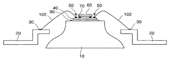
- FIG. 1 is a cross-sectional view of an LED package according to an embodiment of the prior art.
- the LED package is configured to electrify leading wires through gold wires 102, bonded to a GaN compound chip emitting light, and to discharge heat through an underlying heat sink 10. Further, electricity is supplied to the LED package through metal leads 20 wire-bonded to an external support and an LED package portion, and thus the LED package is configured to emit light.
- the above structure forms one package for each chip 60.
- the above conventional LED package forms a package type of a lead frame type.
- the lead frame type is difficult to integrate the LED chips because it has a low available package region.
- the lead frame type inevitably increases the thickness or an external area of a product when the lead frame type is mounted on the product because a package size for a chip size is relatively large.
- the conventional LED package further requires underlying heat sinks for discharging heat generated from the LED chips, and thus the thickness and volume of the LED package are increased that much.
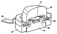
- FIG. 2 is a cross-sectional view of an LED package according to another embodiment of the prior art.
- a plastic lens 25 is used in order to the linearity and photoefficiency of light. This serves as a limit to a reduction in the above-described LED package and generates the cost problem in terms of the process.
- the present invention has been made in view of the above problems, and it is an object of the present invention to provide an optical package and a method of manufacturing the same, which are capable of reducing the volume of the optical package with a low cost, reducing the thickness and an external volume of a final product, and enabling integration and a reduction in the size.
- another object of the present invention is to provide an optical package and a method of manufacturing the same, which can reduce the absorption of light by an insulating layer and can increase luminance and photoefficiency by plating a metal layer, functioning as a heat sink and a support, or plating a light reflective layer and forming a white reflective layer on a top surface or surfaces of the insulating layer or forming a metal reflective layer and a plating layer on the surfaces of the insulating layer.
- an optical package comprises a metal layer configured to have a circuit pattern formed therein, an insulating layer formed on the metal layer and configured to include holes, an optical element mounted on one of the holes, connection units configured to electrically connect the optical element and the circuit pattern, and a resin unit configured to bury the optical element and the connection units. Accordingly, optical packages can be reduced in size and integrated using the insulating film of a tape type without using a lead frame.
- the optical package further comprises a reflective layer formed on part of a surface or the entire surface of the insulating layer. Accordingly, luminance and photoefficiency can be increased through the reflective layer.
- the reflective layer be a white reflective layer or a metal reflective layer.
- the optical package can further comprise a light reflective layer or a plating layer formed on the metal layer exposed through the holes.
- the reflective layer have inclined planes on the sides of the insulating layer so that light is upwardly reflected.
- the white reflective layer bury the sides of the insulating layer in a thickness of 10 ⁇ m to 100 ⁇ m.
- the white reflective layer can be formed by printing any one of a silver paste, a white solder resist, and white epoxy.
- the metal reflective layer include at least one of silver (Ag), nickel (Ni), copper (Cu), platinum (Pt), palladium (Pd), and gold (Au).
- the light reflective layer or the plating layer be further formed on the other side of the metal layer having the insulating layer stacked thereon.
- the light reflective layer can contain silver (Ag), or the plating layer includes at least one of silver (Ag), nickel (Ni), copper (Cu), platinum (Pt), palladium (Pd), and gold (Au).
- the metal layer be a copper (Cu) layer or the insulating layer is a polyimide film.
- the resin unit have a convex lens shape and include a fluorescent substance and a transparent resin.
- the transparent resin be made of silicon (Si).
- a method of manufacturing an optical package comprises the steps of (a) forming holes in an insulating layer, (b) laminating a metal layer below the insulating layer and forming a circuit pattern in the metal layer, (c) mounting an optical element on one of the holes and electrically connecting the optical element and the circuit pattern through connection units, and (d) forming a resin unit for burying the optical element and the connection units.
- the optical package can further comprise the step (b') of forming a reflective layer on part of a surface or an entire surface of the insulating layer, after the step (b).
- step (b') include forming a white reflective layer or a metal reflective layer.
- the method can further comprise the step (b-1) of forming a light reflective layer on the metal layer exposed through the holes, after the step (b).
- the method can further comprise the step (b-2) of forming a plating layer on the metal layer exposed through the holes, after the step (b).
- step (b-1) further include forming the light reflective layer on the other side having the insulating layer stacked thereon.
- step (b-2) further include forming a plating layer on the other side having the insulating layer stacked thereon.
- the entire volume and thickness of a package can be reduced by forming a package according to the existing lead frame method through a package using a tape substrate. Further, packages with a high degree of integration can be produced by forming a package of a surface emitting method in a dot-emitting method. Furthermore, the cost can be reduced, the process can be simplified, and the productivity can be improved by performing an encapsulation process and a process of forming a lens shape at the same time. Luminance and photoefficiency can be improved through a plated light reflective layer and a plated white reflective layer or a metal reflective layer and a plating layer formed on the surface of an insulating layer.
- FIG. 1 is a cross-sectional view of an LED package according to an embodiment of the prior art
- FIG. 2 is a cross-sectional view of an LED package according to another embodiment of the prior art
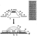
- FIG. 3 is a cross-sectional view showing a comparison of an LED package according to an embodiment of the prior art and an optical package according to an embodiment of the present invention
- FIGS. 4 to 6 are cross-sectional views showing an optical package according to another embodiment of the present invention.
- FIG. 7 is a top view of the polyimide face and the circuit pattern unit of the optical package according to an embodiment of the present invention.
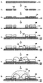
- FIG. 8 is a cross-sectional view illustrating a process of manufacturing the optical package according to an embodiment of the present invention.
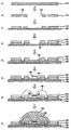
- FIGS. 9 and 10 are cross-sectional views illustrating a process of manufacturing the optical package according to another embodiment of the present invention.
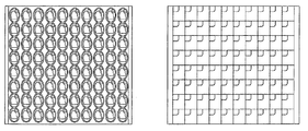
- FIG. 11 is a cross-sectional view and a top view, in detail, showing the degree of integration of optical packages according to the prior art and the present invention.
- FIG. 3 is a cross-sectional view showing a comparison of an LED package according to an embodiment of the prior art and an optical package according to an embodiment of the present invention
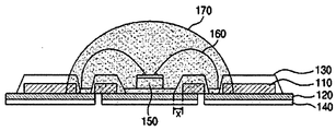
- FIGS. 4 to 6 are cross-sectional views showing an optical package according to another embodiment of the present invention.
- an insulating layer 110 including holes is formed on a metal layer 120 having a circuit pattern formed therein.
- the structure further includes an optical element 150 mounted on the holes, connection units 160 configured to electrically connect the optical element 150 and the circuit pattern, and a resin unit 170 configured to bury the optical element 150 and the connection units 160.
- a white reflective layer 130 i.e., a reflective layer
- a light reflective layer 140 be plated on the metal layer 120 exposed through the holes.
- the insulating layer 110 be a polyimide film and the metal layer 120 be made of copper (Cu).
- the white reflective layer 130 is formed on the top surface of the insulating layer 110. It is preferred that the white reflective layer 130 be formed by printing any one of silver paste, a white solder resist, and white epoxy white epoxy.
- the white reflective layer 130 not a green-series solder resist is formed on the top surface of the insulating layer 110 in order to increase brightness.
- the white reflective layer 130 can be formed not only on the surface (i.e., the top surface) of the insulating layer 110, but also on the sides of the insulating layer 110, as shown in FIG. 4 or 5. It is preferred that the sides of the insulating layer 110 be buried in a thickness of 10 ⁇ m to 100 ⁇ m.
- the white reflective layer 130 has inclined planes on the sides of the insulating layer 110 so that light generated from the optical element 150 can be better upwardly reflected as shown in FIG. 5, but it is preferred that a distance between the side of the insulating layer 110 and a bottom surface of the inclined plane of the white reflective layer 130 (i.e., X in FIG. 5) be 10 ⁇ m to 100 ⁇ m. As described above, light generated from the optical element 150 through the inclined planes of the white reflective layer 130 is upwardly reflected by the inclined planes of the white reflective layer 130, thereby being capable of increasing photoefficiency.
- the white reflective layer 130 serves as a reflective layer and thus increases photoefficiency. Further, the white reflective layer 130 serves as a barrier rib and functions to partition the boundary, when the resin unit 170 is subsequently formed.
- the light reflective layer 140 may be plated on the metal layer 120 which is exposed through the holes, from the metal layer 120 in which the white reflective layer 130 is not formed. As shown, it is preferred that the light reflective layer 140 be plated on the other side of the metal layer 120 on which the insulating layer 110 is stacked. It is preferred that the plating of the light reflective layer 140 be silver (Ag) or plating including silver (Ag).
- the light reflective layer 140 including silver (Ag) is formed. Accordingly, brightness is improved, thermal conductivity is increased, and a heat dissipation effect according to heat generated from the optical element is increased. Consequently, reflexibility can be increased, the absorption of light can be prevented, and photoefficiency can be maximized.
- an LED chip i.e., the optical element 150
- gold (Au) wires 160 i.e., the connection units
- an LED package type of a tape type in which the LED chip 150 and the wires 160 are buried using the resin unit 170 be performed.
- the resin unit 170 have a convex lens shape and include a fluorescent substance and a transparent resin and the transparent resin be silicon (Si).
- the present invention can implement the integrated optical package having a reduced size through the insulating film 110 of a film type and the underlying circuit pattern layer 120 without using an underlying heat sink and a metal lead portion.
- the circuit pattern layer 120 is formed below the insulating layer 110, and the circuit pattern layer 120 serves as not only a circuit board, but also a heat sink. Further, the wire bonding has an effect in that bonding strength is excellent because of a different in the RZ according to a surface roughness.
- FIG. 6 is a diagram showing a cross-sectional view of an optical package according to another embodiment of the present invention.
- a metal layer 120 having a circuit pattern formed therein exists below an insulating layer 110 having holes formed therein.
- a metal reflective layer 135 is formed on the surfaces of the insulating layer 110, and a plating layer 145 is formed on the metal reflective layer 135 and on the metal layer 120 exposed through the holes.
- the insulating layer 110 be a polyimide film.
- the metal layer 120 be a copper (Cu) layer.
- the metal reflective layer 135 is formed on the surfaces (i.e., a top surface and sides) of the insulating layer 110. It is preferred that the metal reflective layer 135 be printed by coating a conductive paste, such as silver (Ag), nickel (Ni), copper (Cu), palladium (Pd), platinum (Pt), gold (Au), or carbon. It is most preferred that the metal reflective layer 135 be printed by coating silver paste from among the conductive pastes.
- a conductive paste such as silver (Ag), nickel (Ni), copper (Cu), palladium (Pd), platinum (Pt), gold (Au), or carbon. It is most preferred that the metal reflective layer 135 be printed by coating silver paste from among the conductive pastes.
- Common polyimide has a brown color or a yellow-series color. The polyimide is problematic in that it has low brightness because it absorbs light rather it reflects light.
- the metal reflective layer 135 and the plating layer 145 are formed not only on the top surface of the polyimide layer 110, but also on the sides therereof.
- the absorption of light by the polyimide layer 110 can be reduced, and photoefficiency can be increased.
- the metal reflective layer 135 be formed such that the insulating layer 110 is buried in a right angle form of a barrier rib shape, but such that the barrier rib has an angle (that is, an inclined plane) on the sides of the insulating layer 110, as shown in FIG. 6. Accordingly, light generated from an optical element 150 via the inclined planes of the metal reflective layer 135 is upwardly reflected by the inclined planes of the metal reflective layer 135, thereby being capable of increasing photoefficiency.
- the plating layer 145 may be formed on the metal reflective layer 135 and the metal layer 120 exposed through the holes. It is preferred that, as shown in FIG. 6, the plating layer 145 be plated on the other side of the metal layer 120 having the insulating layer 110 stacked thereon. It is preferred that the plating layer 145 be made of any one of silver (Ag), nickel (Ni), copper (Cu), palladium (Pd), platinum (Pt), and gold (Au). As described above, not gold (Au) plating for wire bonding, but the silver (Ag), nickel (Ni), copper (Cu), palladium (Pd), platinum (Pt), or gold (Au) plating layer 140 is formed. Accordingly, brightness is improved, thermal conductivity is increased, and a heat dissipation effect according to heat generated from the LED chip is increased. Consequently, reflexibility can be increased, the absorption of light can be prevented, and photoefficiency can be maximized.
- connection units 160 connection units 160
- resin unit 170 in FIG. 6 are the same as those of FIGS. 3 to 5, and descriptions thereof are omitted.
- FIG. 7 is a top view of the polyimide face and the circuit pattern of an optical package according to an embodiment of the present invention. As shown in FIG. 7, the optical package of the present invention is excellent in the degree of integration as compared with a top view of the conventional LED package (refer to the figure on the right side of FIG. 3).
- FIGS. 8 and 9 are cross-sectional views illustrating a process of manufacturing the optical package according to another embodiment of the present invention.
- holes 115 and 116 are formed in the insulating film 110 through punching (S2, P2). It is preferred that the insulating film 110 be a polyimide film.
- the holes 115 and 116 include a device hole 115 (i.e., a center hole where the optical element will be placed) and via holes 116 to which wires (i.e., the connection units 160) will be bonded in order to supply a power source to the optical element 150.
- the metal layer 120 is laminated (S3, P3). It is preferred that the metal layer 120 be made of copper (Cu).
- a photoresist is coated on the surface, and exposure and development processes are performed. After the development process is completed, necessary circuits are formed through an etching process, and the photoresist is peeled off, thereby forming the circuit pattern layer 120.
- the white reflective layer 130 is formed on the insulating layer 110 other than a surface for bonding and the via holes for the supply of an external power source (S4).
- polyimide In general, polyimide is electrically stable, but is problematic in that it has poor reflexibility because of its brown or yellow-series color and thus has low photoefficiency. Photoefficiency can be increased by putting color through the white reflective layer 130. It is preferred that the white reflective layer 130 be printed by coating any one of a silver paste, a white solder resist, and white epoxy not a common green-series solder resist.
- the white reflective layer 130 be formed not only on the top surface of the insulating layer 110, but also on the sides of the insulating layer 110, as shown in FIG. 9, in order to improve brightness and photoefficiency (P4). It is more effective to increase luminance and photoefficiency when the white reflective layer 130 buries the sides of the insulating layer 110 in a thickness of 10 ⁇ m to 100 ⁇ m.
- the insulating layer 110 may be buried in a right angle form of a barrier rib form as shown in FIG. 4, it is preferred that the inclined planes be formed on the sides of the insulating layer 110 so that light generated from the optical element 150 is upwardly reflected as shown in FIG. 9. It is preferred that a distance between the side of the insulating layer 110 and a bottom surface of the inclined plane of the white reflective layer 130 (i.e., X in FIG. 9) be 10 ⁇ m to 100 ⁇ m.
- the light reflective layer 140 is formed by plating the metal layer 120 exposed through the underlying via holes 115 and 116 (i.e., the holes) through surface processing so that the metal layer 120 can be bonded (S5, P5).
- the light reflective layer 140 also be plated on a circuit face (i.e., the other side of the metal layer 120 on which the insulating layer 110 is stacked) as shown in the drawings.
- the plating of the light reflective layer 140 be silver (Ag) or plating including silver (Ag). Since not gold (Au) plating, but silver (Ag) plating is performed as described above, the absorption of light by the polyimide film 110 can be reduced, and photoefficiency can be increased.
- the optical element 150 is mounted on the plated light reflective layer 140 where the optical element 150 will be placed, in the via hole formed in the insulating layer 110, through die bonding (S6, P6). It is preferred that the optical element 150 (i.e., an LED chip) be mounted using adhesives.
- the gold (Au) wires 160 are bonded to the light reflective layer 140 plated with silver (Ag), thereby electrically connecting the circuit pattern layer 120 and the LED chip 150 (S7, P7).
- the resin unit 170 is formed to bury the LED chip 150 and the Au wires 160 (S8, P8).
- the resin unit 170 of a convex lens shape is formed by excessively coating a fluorescent substance and a transparent resin for a white LED at the boundary portion of the white solder resist, thereby completing the optical package.
- the resin unit 170 of a convex lens shape such as that shown in drawings, is formed because of surface tension. Accordingly, the existing encapsulation process and the existing process of forming the plastic lens shape can be performed at the same time.
- FIG. 10 is a cross-sectional view illustrating a process of manufacturing the optical package according to another embodiment of the present invention. Steps Q1 to Q3 and Q6 to Q8 in FIG. 10 are similar to the steps S1 (P1) to S3 (P3), and S6 (P6) to S8 (P8), and thus differences Q4 and Q5 are chiefly described.
- the holes 115 and 116 are formed in the insulating film 110 through punching (Q2).
- the metal layer 120 is laminated to form the circuit pattern layer 120 (Q3).
- the metal reflective layer 135 (i.e., a reflective layer) is formed on part of the entire insulating layer 110 (Q4). It is preferred that the metal reflective layer 135 be printed by coating a conductive paste, such as silver (Ag), nickel (Ni), copper (Cu), palladium (Pd), platinum (Pt), gold (Au), or carbon. It is most preferred that the metal reflective layer 135 be printed by coating the silver (Ag) paste.
- the insulating layer 110 may be buried in a right angle form of a barrier rib form, it is preferred that the inclined planes be formed on the sides of the insulating layer 110 so that light generated from the optical element 150 is upwardly reflected as shown in FIG. 10.
- the plating layer 145 is formed on the metal reflective layer 135 and on the metal layer 120, exposed through the holes 115 and 116, through surface processing so that it can be bonded (Q5).
- the plating layer 145 also be formed on a circuit face (i.e., the other side of the metal layer 120 having the insulating layer 110 staked thereon) as shown in FIG. 10.
- the plating layer 145 be made of silver (Ag), nickel (Ni), copper (Cu), palladium (Pd), platinum (Pt), or gold (Au).
- polyimide is electrically stable, but is problematic in that it has poor reflexibility because of its brown or yellow-series color and thus has low photoefficiency.
- the polyimide regions 110 disappear, brilliance is increased through the plating layer 145 as described above, and photoefficiency can be further increased.
- the steps following the step Q6 are similar to those of FIGS. 8 and 9 as described above, and descriptions thereof are omitted.
- FIG. 11 is a cross-sectional view and a top view, in detail, showing the degree of integration of optical packages according to the prior art and the present invention. From FIG. 11, it can be seen that in case where LED packages are formed in the same area, a larger number of LED packages can be formed in the case of the present invention (refer to the drawing on the right side of FIG. 11), as compared with the arrangement of LED chips each having the metal lead portion 20 and the lower heat sink 10 (refer to FIG. 3 and the drawing on the left side of FIG. 11).
Landscapes
- Led Device Packages (AREA)
Abstract
The present invention relates to an optical package and a method of manufacturing the same, which are capable of reducing the entire volume and thickness of the package by forming a package according to the existing lead frame method through a package using a tape substrate and of producing packages with a high degree of integration by forming a package of a surface emitting method in a dot-emitting method. Further, in accordance with the present invention, luminance and photoefficiency can be increased through a light reflective layer and a white reflective layer or a metal reflective layer and a plating layer.
Description
The present invention relates to an optical package and a method of manufacturing the same, and more particularly, to an optical package and a method of manufacturing the same, which are capable of reducing the volume and thickness of the package, increasing the degree of integration, and improving luminance and photoefficiency.
A Light Emitting Diode (LED) refers to an intermetallic compound junction diode which produces minority carriers (i.e., electrons or holes) injected using a p-n junction structure of semiconductors and emits light by changing electric energy into light energy through a recombination of the carriers. That is, when forward voltage is applied to a semiconductor of a specific element, electrons and holes are moved through the junction of a positive pole and a negative pole and then recombined. Energy when the electrons and holes are recombined is smaller than energy when the electrons and the holes are separated from each other. Accordingly, the LED emits light because of a difference in the energy. The LED is being used for not only common display devices, but also lighting devices or the backlight elements of LCDs, and the applications of the LED are gradually widened. In particular, the LED has advantages of being driven with a relatively low voltage, having low generation of heat because of high energy efficiency, and having a long lifespan. It is expected that as technology capable of providing white light of high brightness which was difficult to be implemented conventionally is developed, the LED can replace current most light source devices.
FIG. 1 is a cross-sectional view of an LED package according to an embodiment of the prior art. Referring to FIG. 1, the LED package is configured to electrify leading wires through gold wires 102, bonded to a GaN compound chip emitting light, and to discharge heat through an underlying heat sink 10. Further, electricity is supplied to the LED package through metal leads 20 wire-bonded to an external support and an LED package portion, and thus the LED package is configured to emit light. The above structure forms one package for each chip 60.
The above conventional LED package forms a package type of a lead frame type. However, the lead frame type is difficult to integrate the LED chips because it has a low available package region. Further, the lead frame type inevitably increases the thickness or an external area of a product when the lead frame type is mounted on the product because a package size for a chip size is relatively large.
Further, the conventional LED package further requires underlying heat sinks for discharging heat generated from the LED chips, and thus the thickness and volume of the LED package are increased that much.
FIG. 2 is a cross-sectional view of an LED package according to another embodiment of the prior art.
Referring to FIG. 2, in an encapsulation process of protecting the bonding of wires 102, after a fluorescent substance and a resin complex are coated, a plastic lens 25 is used in order to the linearity and photoefficiency of light. This serves as a limit to a reduction in the above-described LED package and generates the cost problem in terms of the process.
Accordingly, there is a need for technology which can manufacture an LED package with a low cost, a more reduced size, and a simplified process.
Accordingly, the present invention has been made in view of the above problems, and it is an object of the present invention to provide an optical package and a method of manufacturing the same, which are capable of reducing the volume of the optical package with a low cost, reducing the thickness and an external volume of a final product, and enabling integration and a reduction in the size. Further, another object of the present invention is to provide an optical package and a method of manufacturing the same, which can reduce the absorption of light by an insulating layer and can increase luminance and photoefficiency by plating a metal layer, functioning as a heat sink and a support, or plating a light reflective layer and forming a white reflective layer on a top surface or surfaces of the insulating layer or forming a metal reflective layer and a plating layer on the surfaces of the insulating layer.
To achieve the above objects, an optical package according to an embodiment of the present invention comprises a metal layer configured to have a circuit pattern formed therein, an insulating layer formed on the metal layer and configured to include holes, an optical element mounted on one of the holes, connection units configured to electrically connect the optical element and the circuit pattern, and a resin unit configured to bury the optical element and the connection units. Accordingly, optical packages can be reduced in size and integrated using the insulating film of a tape type without using a lead frame.
In particular, the optical package further comprises a reflective layer formed on part of a surface or the entire surface of the insulating layer. Accordingly, luminance and photoefficiency can be increased through the reflective layer.
Further, it is preferred that the reflective layer be a white reflective layer or a metal reflective layer.
Further, the optical package can further comprise a light reflective layer or a plating layer formed on the metal layer exposed through the holes.
Further, it is preferred that the reflective layer have inclined planes on the sides of the insulating layer so that light is upwardly reflected.
Further, it is preferred that the white reflective layer bury the sides of the insulating layer in a thickness of 10 ㎛ to 100 ㎛.
Further, the white reflective layer can be formed by printing any one of a silver paste, a white solder resist, and white epoxy.
Further, it is preferred that the metal reflective layer include at least one of silver (Ag), nickel (Ni), copper (Cu), platinum (Pt), palladium (Pd), and gold (Au).
Further, it is preferred that the light reflective layer or the plating layer be further formed on the other side of the metal layer having the insulating layer stacked thereon.
Further, the light reflective layer can contain silver (Ag), or the plating layer includes at least one of silver (Ag), nickel (Ni), copper (Cu), platinum (Pt), palladium (Pd), and gold (Au).
Further, it is preferred that the metal layer be a copper (Cu) layer or the insulating layer is a polyimide film.
Further, it is preferred that the resin unit have a convex lens shape and include a fluorescent substance and a transparent resin.
Further, it is preferred that the transparent resin be made of silicon (Si).
A method of manufacturing an optical package according to an embodiment of the present invention comprises the steps of (a) forming holes in an insulating layer, (b) laminating a metal layer below the insulating layer and forming a circuit pattern in the metal layer, (c) mounting an optical element on one of the holes and electrically connecting the optical element and the circuit pattern through connection units, and (d) forming a resin unit for burying the optical element and the connection units.
In particular, the optical package can further comprise the step (b') of forming a reflective layer on part of a surface or an entire surface of the insulating layer, after the step (b).
Further, it is preferred that the step (b') include forming a white reflective layer or a metal reflective layer.
Further, the method can further comprise the step (b-1) of forming a light reflective layer on the metal layer exposed through the holes, after the step (b).
Further, the method can further comprise the step (b-2) of forming a plating layer on the metal layer exposed through the holes, after the step (b).
Further, it is preferred that the step (b-1) further include forming the light reflective layer on the other side having the insulating layer stacked thereon.
Further, it is preferred that the step (b-2) further include forming a plating layer on the other side having the insulating layer stacked thereon.
In accordance with the present invention, the entire volume and thickness of a package can be reduced by forming a package according to the existing lead frame method through a package using a tape substrate. Further, packages with a high degree of integration can be produced by forming a package of a surface emitting method in a dot-emitting method. Furthermore, the cost can be reduced, the process can be simplified, and the productivity can be improved by performing an encapsulation process and a process of forming a lens shape at the same time. Luminance and photoefficiency can be improved through a plated light reflective layer and a plated white reflective layer or a metal reflective layer and a plating layer formed on the surface of an insulating layer.
FIG. 1 is a cross-sectional view of an LED package according to an embodiment of the prior art;
FIG. 2 is a cross-sectional view of an LED package according to another embodiment of the prior art;
FIG. 3 is a cross-sectional view showing a comparison of an LED package according to an embodiment of the prior art and an optical package according to an embodiment of the present invention;
FIGS. 4 to 6 are cross-sectional views showing an optical package according to another embodiment of the present invention;
FIG. 7 is a top view of the polyimide face and the circuit pattern unit of the optical package according to an embodiment of the present invention;
FIG. 8 is a cross-sectional view illustrating a process of manufacturing the optical package according to an embodiment of the present invention;
FIGS. 9 and 10 are cross-sectional views illustrating a process of manufacturing the optical package according to another embodiment of the present invention; and
FIG. 11 is a cross-sectional view and a top view, in detail, showing the degree of integration of optical packages according to the prior art and the present invention.
Hereinafter, some preferred embodiments of the present invention are described in detail with reference to the accompanying drawings. However, the present invention can be modified in various forms and should not be construed to be limited to the following embodiments. The embodiments of the present invention are provided to those skilled in the art in order to more fully describe the embodiments. Accordingly, in the drawings, the shape, etc. of an element has been enlarged for clarity, and the same reference numbers are used throughout the drawings to refer to the same parts.
FIG. 3 is a cross-sectional view showing a comparison of an LED package according to an embodiment of the prior art and an optical package according to an embodiment of the present invention, and FIGS. 4 to 6 are cross-sectional views showing an optical package according to another embodiment of the present invention.
As shown in FIG. 3, in the package structure of the present invention, an insulating layer 110 including holes is formed on a metal layer 120 having a circuit pattern formed therein. The structure further includes an optical element 150 mounted on the holes, connection units 160 configured to electrically connect the optical element 150 and the circuit pattern, and a resin unit 170 configured to bury the optical element 150 and the connection units 160. A white reflective layer 130 (i.e., a reflective layer) is formed on a top surface of the insulating layer 110. It is preferred that a light reflective layer 140 be plated on the metal layer 120 exposed through the holes. Here, it is preferred that the insulating layer 110 be a polyimide film and the metal layer 120 be made of copper (Cu). In the present invention, the white reflective layer 130 is formed on the top surface of the insulating layer 110. It is preferred that the white reflective layer 130 be formed by printing any one of silver paste, a white solder resist, and white epoxy white epoxy.
Common polyimide has a brown color or a yellow-series color. The polyimide is problematic in that it has low brightness because it absorbs light rather it reflects light. Accordingly, the white reflective layer 130 not a green-series solder resist is formed on the top surface of the insulating layer 110 in order to increase brightness. In order to further increase brightness, the white reflective layer 130 can be formed not only on the surface (i.e., the top surface) of the insulating layer 110, but also on the sides of the insulating layer 110, as shown in FIG. 4 or 5. It is preferred that the sides of the insulating layer 110 be buried in a thickness of 10 ㎛ to 100 ㎛. The white reflective layer 130 has inclined planes on the sides of the insulating layer 110 so that light generated from the optical element 150 can be better upwardly reflected as shown in FIG. 5, but it is preferred that a distance between the side of the insulating layer 110 and a bottom surface of the inclined plane of the white reflective layer 130 (i.e., X in FIG. 5) be 10 ㎛ to 100 ㎛. As described above, light generated from the optical element 150 through the inclined planes of the white reflective layer 130 is upwardly reflected by the inclined planes of the white reflective layer 130, thereby being capable of increasing photoefficiency. The white reflective layer 130 serves as a reflective layer and thus increases photoefficiency. Further, the white reflective layer 130 serves as a barrier rib and functions to partition the boundary, when the resin unit 170 is subsequently formed.
Further, the light reflective layer 140 may be plated on the metal layer 120 which is exposed through the holes, from the metal layer 120 in which the white reflective layer 130 is not formed. As shown, it is preferred that the light reflective layer 140 be plated on the other side of the metal layer 120 on which the insulating layer 110 is stacked. It is preferred that the plating of the light reflective layer 140 be silver (Ag) or plating including silver (Ag).
As described above, not gold (Au) plating for wire bonding, but the light reflective layer 140 including silver (Ag), is formed. Accordingly, brightness is improved, thermal conductivity is increased, and a heat dissipation effect according to heat generated from the optical element is increased. Consequently, reflexibility can be increased, the absorption of light can be prevented, and photoefficiency can be maximized. Furthermore, in the present invention, it is preferred that an LED chip (i.e., the optical element 150) be mounted on the light reflective layer 140, gold (Au) wires 160 (i.e., the connection units) for an electrical connection between the chip 150 and the circuit pattern be bonded, and an LED package type of a tape type in which the LED chip 150 and the wires 160 are buried using the resin unit 170 be performed. It is preferred that the resin unit 170 have a convex lens shape and include a fluorescent substance and a transparent resin and the transparent resin be silicon (Si). As described above, the present invention can implement the integrated optical package having a reduced size through the insulating film 110 of a film type and the underlying circuit pattern layer 120 without using an underlying heat sink and a metal lead portion. Further, the circuit pattern layer 120 is formed below the insulating layer 110, and the circuit pattern layer 120 serves as not only a circuit board, but also a heat sink. Further, the wire bonding has an effect in that bonding strength is excellent because of a different in the RZ according to a surface roughness.
FIG. 6 is a diagram showing a cross-sectional view of an optical package according to another embodiment of the present invention. Referring to FIG. 6, in the package structure of the present invention, a metal layer 120 having a circuit pattern formed therein exists below an insulating layer 110 having holes formed therein. Further, a metal reflective layer 135 is formed on the surfaces of the insulating layer 110, and a plating layer 145 is formed on the metal reflective layer 135 and on the metal layer 120 exposed through the holes. It is preferred that the insulating layer 110 be a polyimide film. It is also preferred that the metal layer 120 be a copper (Cu) layer. Further, in the present embodiment, as described above, the metal reflective layer 135 is formed on the surfaces (i.e., a top surface and sides) of the insulating layer 110. It is preferred that the metal reflective layer 135 be printed by coating a conductive paste, such as silver (Ag), nickel (Ni), copper (Cu), palladium (Pd), platinum (Pt), gold (Au), or carbon. It is most preferred that the metal reflective layer 135 be printed by coating silver paste from among the conductive pastes. Common polyimide has a brown color or a yellow-series color. The polyimide is problematic in that it has low brightness because it absorbs light rather it reflects light. For this reason, the metal reflective layer 135 and the plating layer 145 are formed not only on the top surface of the polyimide layer 110, but also on the sides therereof. Thus, the absorption of light by the polyimide layer 110 can be reduced, and photoefficiency can be increased. It is preferred that the metal reflective layer 135 be formed such that the insulating layer 110 is buried in a right angle form of a barrier rib shape, but such that the barrier rib has an angle (that is, an inclined plane) on the sides of the insulating layer 110, as shown in FIG. 6. Accordingly, light generated from an optical element 150 via the inclined planes of the metal reflective layer 135 is upwardly reflected by the inclined planes of the metal reflective layer 135, thereby being capable of increasing photoefficiency. Further, the plating layer 145, as described above, may be formed on the metal reflective layer 135 and the metal layer 120 exposed through the holes. It is preferred that, as shown in FIG. 6, the plating layer 145 be plated on the other side of the metal layer 120 having the insulating layer 110 stacked thereon. It is preferred that the plating layer 145 be made of any one of silver (Ag), nickel (Ni), copper (Cu), palladium (Pd), platinum (Pt), and gold (Au). As described above, not gold (Au) plating for wire bonding, but the silver (Ag), nickel (Ni), copper (Cu), palladium (Pd), platinum (Pt), or gold (Au) plating layer 140 is formed. Accordingly, brightness is improved, thermal conductivity is increased, and a heat dissipation effect according to heat generated from the LED chip is increased. Consequently, reflexibility can be increased, the absorption of light can be prevented, and photoefficiency can be maximized.
The optical element 150, connection units 160, and a resin unit 170 in FIG. 6 are the same as those of FIGS. 3 to 5, and descriptions thereof are omitted.
FIG. 7 is a top view of the polyimide face and the circuit pattern of an optical package according to an embodiment of the present invention. As shown in FIG. 7, the optical package of the present invention is excellent in the degree of integration as compared with a top view of the conventional LED package (refer to the figure on the right side of FIG. 3).
FIGS. 8 and 9 are cross-sectional views illustrating a process of manufacturing the optical package according to another embodiment of the present invention. Referring to FIGS. 8 and 9, first, holes 115 and 116 are formed in the insulating film 110 through punching (S2, P2). It is preferred that the insulating film 110 be a polyimide film. The holes 115 and 116 include a device hole 115 (i.e., a center hole where the optical element will be placed) and via holes 116 to which wires (i.e., the connection units 160) will be bonded in order to supply a power source to the optical element 150.
Next, the metal layer 120 is laminated (S3, P3). It is preferred that the metal layer 120 be made of copper (Cu). Next, after a surface is activated through several chemical processing, a photoresist is coated on the surface, and exposure and development processes are performed. After the development process is completed, necessary circuits are formed through an etching process, and the photoresist is peeled off, thereby forming the circuit pattern layer 120. Next, the white reflective layer 130 is formed on the insulating layer 110 other than a surface for bonding and the via holes for the supply of an external power source (S4).
In general, polyimide is electrically stable, but is problematic in that it has poor reflexibility because of its brown or yellow-series color and thus has low photoefficiency. Photoefficiency can be increased by putting color through the white reflective layer 130. It is preferred that the white reflective layer 130 be printed by coating any one of a silver paste, a white solder resist, and white epoxy not a common green-series solder resist.
It is preferred that the white reflective layer 130 be formed not only on the top surface of the insulating layer 110, but also on the sides of the insulating layer 110, as shown in FIG. 9, in order to improve brightness and photoefficiency (P4). It is more effective to increase luminance and photoefficiency when the white reflective layer 130 buries the sides of the insulating layer 110 in a thickness of 10 ㎛ to 100 ㎛. In particular, although the insulating layer 110 may be buried in a right angle form of a barrier rib form as shown in FIG. 4, it is preferred that the inclined planes be formed on the sides of the insulating layer 110 so that light generated from the optical element 150 is upwardly reflected as shown in FIG. 9. It is preferred that a distance between the side of the insulating layer 110 and a bottom surface of the inclined plane of the white reflective layer 130 (i.e., X in FIG. 9) be 10 ㎛ to 100 ㎛.
Next, the light reflective layer 140 is formed by plating the metal layer 120 exposed through the underlying via holes 115 and 116 (i.e., the holes) through surface processing so that the metal layer 120 can be bonded (S5, P5). Here, it is preferred that the light reflective layer 140 also be plated on a circuit face (i.e., the other side of the metal layer 120 on which the insulating layer 110 is stacked) as shown in the drawings. Further, it is preferred that the plating of the light reflective layer 140 be silver (Ag) or plating including silver (Ag). Since not gold (Au) plating, but silver (Ag) plating is performed as described above, the absorption of light by the polyimide film 110 can be reduced, and photoefficiency can be increased.
Next, the optical element 150 is mounted on the plated light reflective layer 140 where the optical element 150 will be placed, in the via hole formed in the insulating layer 110, through die bonding (S6, P6). It is preferred that the optical element 150 (i.e., an LED chip) be mounted using adhesives. Next, the gold (Au) wires 160 are bonded to the light reflective layer 140 plated with silver (Ag), thereby electrically connecting the circuit pattern layer 120 and the LED chip 150 (S7, P7). Next, the resin unit 170 is formed to bury the LED chip 150 and the Au wires 160 (S8, P8). More particularly, the resin unit 170 of a convex lens shape is formed by excessively coating a fluorescent substance and a transparent resin for a white LED at the boundary portion of the white solder resist, thereby completing the optical package. In case where the fluorescent substance and the transparent resin are excessively coated, the resin unit 170 of a convex lens shape, such as that shown in drawings, is formed because of surface tension. Accordingly, the existing encapsulation process and the existing process of forming the plastic lens shape can be performed at the same time.
FIG. 10 is a cross-sectional view illustrating a process of manufacturing the optical package according to another embodiment of the present invention. Steps Q1 to Q3 and Q6 to Q8 in FIG. 10 are similar to the steps S1 (P1) to S3 (P3), and S6 (P6) to S8 (P8), and thus differences Q4 and Q5 are chiefly described. First, the holes 115 and 116 are formed in the insulating film 110 through punching (Q2). The metal layer 120 is laminated to form the circuit pattern layer 120 (Q3).
Next, the metal reflective layer 135 (i.e., a reflective layer) is formed on part of the entire insulating layer 110 (Q4). It is preferred that the metal reflective layer 135 be printed by coating a conductive paste, such as silver (Ag), nickel (Ni), copper (Cu), palladium (Pd), platinum (Pt), gold (Au), or carbon. It is most preferred that the metal reflective layer 135 be printed by coating the silver (Ag) paste. Although the insulating layer 110 may be buried in a right angle form of a barrier rib form, it is preferred that the inclined planes be formed on the sides of the insulating layer 110 so that light generated from the optical element 150 is upwardly reflected as shown in FIG. 10. Next, the plating layer 145 is formed on the metal reflective layer 135 and on the metal layer 120, exposed through the holes 115 and 116, through surface processing so that it can be bonded (Q5). Here, it is preferred that the plating layer 145 also be formed on a circuit face (i.e., the other side of the metal layer 120 having the insulating layer 110 staked thereon) as shown in FIG. 10. Further, it is preferred that the plating layer 145 be made of silver (Ag), nickel (Ni), copper (Cu), palladium (Pd), platinum (Pt), or gold (Au). In general, polyimide is electrically stable, but is problematic in that it has poor reflexibility because of its brown or yellow-series color and thus has low photoefficiency. Accordingly, if a silver (Ag) paste is coated as in the present invention, the polyimide regions 110 disappear, brilliance is increased through the plating layer 145 as described above, and photoefficiency can be further increased. The steps following the step Q6 are similar to those of FIGS. 8 and 9 as described above, and descriptions thereof are omitted.
FIG. 11 is a cross-sectional view and a top view, in detail, showing the degree of integration of optical packages according to the prior art and the present invention. From FIG. 11, it can be seen that in case where LED packages are formed in the same area, a larger number of LED packages can be formed in the case of the present invention (refer to the drawing on the right side of FIG. 11), as compared with the arrangement of LED chips each having the metal lead portion 20 and the lower heat sink 10 (refer to FIG. 3 and the drawing on the left side of FIG. 11).
The most suitable embodiments have been disclosed in the drawings and specification. Although the specific terms have been used, they are used for the purpose of merely describing the present invention, but are not used to limit their meanings or the scope of the present invention written in the claims. Thus, those skilled in the art will understand that a variety of modifications and other equivalent embodiments can be possible from the above embodiments. Accordingly, the true technical scope of the present invention should be defined by the appended claims.
Claims (20)
- An optical package, comprising:a metal layer configured to have a circuit pattern formed therein;an insulating layer formed on the metal layer and configured to include holes;an optical element mounted on one of the holes;connection units configured to electrically connect the optical element and the circuit pattern; anda resin unit configured to bury the optical element and the connection units.
- The optical package of claim 1, further comprising a reflective layer formed on part of a surface or an entire surface of the insulating layer.
- The optical package of claim 2, wherein the reflective layer is a white reflective layer or a metal reflective layer.
- The optical package of claim 1, further comprising a light reflective layer or a plating layer formed on the metal layer exposed through the holes.
- The optical package of claim 2, wherein the reflective layer has inclined planes on sides of the insulating layer so that light is upwardly reflected.
- The optical package of claim 3, wherein the white reflective layer buries sides of the insulating layer in a thickness of 10 ㎛ to 100 ㎛.
- The optical package of claim 3, wherein the white reflective layer is formed by printing any one of a silver paste, a white solder resist, and white epoxy.
- The optical package of claim 3, wherein the metal reflective layer includes at least one of silver (Ag), nickel (Ni), copper (Cu), platinum (Pt), palladium (Pd), and gold (Au).
- The optical package of claim 4, wherein the light reflective layer or the plating layer is further formed on the other side of the metal layer having the insulating layer stacked thereon.
- The optical package of claim 4 or 9, wherein the light reflective layer contains silver (Ag), or the plating layer includes at least one of silver (Ag), nickel (Ni), copper (Cu), platinum (Pt), palladium (Pd), and gold (Au).
- The optical package of claim 1, wherein the metal layer is a copper (Cu) layer or the insulating layer is a polyimide film.
- The optical package of claim 1, wherein the resin unit has a convex lens shape and includes a fluorescent substance and a transparent resin.
- The optical package of claim 12, wherein the transparent resin is made of silicon (Si).
- A method of manufacturing an optical package, comprising the steps of:(a) forming holes in an insulating layer;(b) laminating a metal layer below the insulating layer and forming a circuit pattern in the metal layer;(c) mounting an optical element on one of the holes and electrically connecting the optical element and the circuit pattern through connection units; and(d) forming a resin unit for burying the optical element and the connection units.
- The method of claim 14, further comprising the step (b') of forming a reflective layer on part of a surface or an entire surface of the insulating layer, after the step (b).
- The method of claim 15, wherein the step (b') includes forming a white reflective layer or a metal reflective layer.
- The method of claim 14, further comprising the step (b-1) of forming a light reflective layer on the metal layer exposed through the holes, after the step (b).
- The method of claim 14, further comprising the step (b-2) of forming a plating layer on the metal layer exposed through the holes, after the step (b).
- The method of claim 17, wherein the step (b-1) further includes forming the light reflective layer on the other side having the insulating layer stacked thereon.
- The method of claim 18, wherein the step (b-2) further includes forming a plating layer on the other side having the insulating layer stacked thereon.
Applications Claiming Priority (8)
| Application Number | Priority Date | Filing Date | Title |
|---|---|---|---|
| KR1020100039715A KR101129002B1 (en) | 2010-04-28 | 2010-04-28 | Optical package and manufacturing method of the same |
| KR10-2010-0039715 | 2010-04-28 | ||
| KR1020100042047A KR101146656B1 (en) | 2010-05-04 | 2010-05-04 | Optical package and manufacturing method of the same |
| KR1020100042044A KR101136392B1 (en) | 2010-05-04 | 2010-05-04 | Optical package and manufacturing method of the same |
| KR10-2010-0042045 | 2010-05-04 | ||
| KR1020100042045A KR101146659B1 (en) | 2010-05-04 | 2010-05-04 | Optical package and manufacturing method of the same |
| KR10-2010-0042047 | 2010-05-04 | ||
| KR10-2010-0042044 | 2010-05-04 |
Publications (1)
| Publication Number | Publication Date |
|---|---|
| WO2011136446A1 true WO2011136446A1 (en) | 2011-11-03 |
Family
ID=44861716
Family Applications (1)
| Application Number | Title | Priority Date | Filing Date |
|---|---|---|---|
| PCT/KR2010/006895 Ceased WO2011136446A1 (en) | 2010-04-28 | 2010-10-08 | Optical package and method of manufacturing the same |
Country Status (2)
| Country | Link |
|---|---|
| TW (1) | TWI472067B (en) |
| WO (1) | WO2011136446A1 (en) |
Cited By (4)
| Publication number | Priority date | Publication date | Assignee | Title |
|---|---|---|---|---|
| WO2013120760A1 (en) * | 2012-02-13 | 2013-08-22 | Tridonic Jennersdorf Gmbh | Led module having a highly reflective carrier |
| EP2626918A3 (en) * | 2012-02-13 | 2013-10-16 | Tridonic Jennersdorf GmbH | LED module with highly reflective support |
| JP2016162972A (en) * | 2015-03-04 | 2016-09-05 | パナソニックIpマネジメント株式会社 | Mounting board and LED module using the same |
| TWI580084B (en) * | 2015-12-31 | 2017-04-21 | 綠點高新科技股份有限公司 | Light-emitting component and manufacturing method thereof |
Families Citing this family (1)
| Publication number | Priority date | Publication date | Assignee | Title |
|---|---|---|---|---|
| TWM579383U (en) * | 2018-12-25 | 2019-06-11 | 同泰電子科技股份有限公司 | Substrate structure with high reflectivity |
Citations (5)
| Publication number | Priority date | Publication date | Assignee | Title |
|---|---|---|---|---|
| KR100853963B1 (en) * | 2007-04-12 | 2008-08-25 | 주식회사 이츠웰 | High Current Surface Mount LED Lamp Using Circuit Board |
| US20080224161A1 (en) * | 2007-03-13 | 2008-09-18 | Sharp Kabushiki Kaisha | Semiconductor Light Emitting Device and Multiple Lead Frame for Semiconductor Light Emitting Device |
| US20090146155A1 (en) * | 2007-12-11 | 2009-06-11 | Foxsemicon Integrated Technology, Inc. | Light-emitting diode |
| US20090206358A1 (en) * | 2008-02-20 | 2009-08-20 | Advanced Optoelectronic Technology Inc. | Package structure of compound semiconductor device and fabricating method thereof |
| WO2009132618A1 (en) * | 2008-04-29 | 2009-11-05 | Osram Opto Semiconductors Gmbh | Surface-mounted led module and method for producing a surface-mounted led module |
Family Cites Families (3)
| Publication number | Priority date | Publication date | Assignee | Title |
|---|---|---|---|---|
| TW200802956A (en) * | 2006-06-16 | 2008-01-01 | Gigno Technology Co Ltd | Light emitting diode module |
| TWI355050B (en) * | 2007-06-22 | 2011-12-21 | Light Ocean Technology Corp | Thin double-sided package substrate and manufactur |
| TWI376819B (en) * | 2008-08-01 | 2012-11-11 | Silicon Base Dev Inc | Photo diode package base structure and manufacturing method of the same |
-
2010
- 2010-10-06 TW TW99133993A patent/TWI472067B/en not_active IP Right Cessation
- 2010-10-08 WO PCT/KR2010/006895 patent/WO2011136446A1/en not_active Ceased
Patent Citations (5)
| Publication number | Priority date | Publication date | Assignee | Title |
|---|---|---|---|---|
| US20080224161A1 (en) * | 2007-03-13 | 2008-09-18 | Sharp Kabushiki Kaisha | Semiconductor Light Emitting Device and Multiple Lead Frame for Semiconductor Light Emitting Device |
| KR100853963B1 (en) * | 2007-04-12 | 2008-08-25 | 주식회사 이츠웰 | High Current Surface Mount LED Lamp Using Circuit Board |
| US20090146155A1 (en) * | 2007-12-11 | 2009-06-11 | Foxsemicon Integrated Technology, Inc. | Light-emitting diode |
| US20090206358A1 (en) * | 2008-02-20 | 2009-08-20 | Advanced Optoelectronic Technology Inc. | Package structure of compound semiconductor device and fabricating method thereof |
| WO2009132618A1 (en) * | 2008-04-29 | 2009-11-05 | Osram Opto Semiconductors Gmbh | Surface-mounted led module and method for producing a surface-mounted led module |
Cited By (5)
| Publication number | Priority date | Publication date | Assignee | Title |
|---|---|---|---|---|
| WO2013120760A1 (en) * | 2012-02-13 | 2013-08-22 | Tridonic Jennersdorf Gmbh | Led module having a highly reflective carrier |
| EP2626918A3 (en) * | 2012-02-13 | 2013-10-16 | Tridonic Jennersdorf GmbH | LED module with highly reflective support |
| US10586901B2 (en) | 2012-02-13 | 2020-03-10 | Tridonic Jennersdorf Gmbh | LED module having a highly reflective carrier |
| JP2016162972A (en) * | 2015-03-04 | 2016-09-05 | パナソニックIpマネジメント株式会社 | Mounting board and LED module using the same |
| TWI580084B (en) * | 2015-12-31 | 2017-04-21 | 綠點高新科技股份有限公司 | Light-emitting component and manufacturing method thereof |
Also Published As
| Publication number | Publication date |
|---|---|
| TWI472067B (en) | 2015-02-01 |
| TW201138163A (en) | 2011-11-01 |
Similar Documents
| Publication | Publication Date | Title |
|---|---|---|
| US8357934B2 (en) | Semiconductor-based sub-mounts for optoelectronic devices with conductive paths | |
| US20110121339A1 (en) | Light-emitting diode module and manufacturing method thereof | |
| CN106783817A (en) | LED package assemblings, LED modules and its manufacture method | |
| WO2011136446A1 (en) | Optical package and method of manufacturing the same | |
| KR101051488B1 (en) | Method for manufacturing light emitting diode unit, and light emitting diode unit manufactured by this method | |
| KR101179579B1 (en) | LED light module and manufacturing methode of thesame | |
| KR101498682B1 (en) | Light emitting diode module | |
| CN220796789U (en) | Laminated packaging structure for realizing integration of control chip and LED light-emitting chip | |
| KR101221568B1 (en) | Backlight Unit having LEDs and Method for manufacturing the same | |
| CN112271175B (en) | LED packaging structure and packaging method | |
| CN101728370B (en) | Encapsulation modular structure of compound semiconductor elements and manufacturing method thereof | |
| TW201123413A (en) | A light emission module with high-efficiency light emission and high-efficiency heat dissipation and applications thereof | |
| KR101051690B1 (en) | Optical package and its manufacturing method | |
| KR101129002B1 (en) | Optical package and manufacturing method of the same | |
| KR101250381B1 (en) | Optical package and manufacturing method of the same | |
| TW201123412A (en) | A light emission module with high-efficiency light emission and high-efficiency heat dissipation and applications thereof | |
| CN201788969U (en) | A light-emitting module and application device with high heat conduction and light conduction functions | |
| KR101146656B1 (en) | Optical package and manufacturing method of the same | |
| CN113471347A (en) | LED embedded packaging substrate and manufacturing method thereof | |
| KR101128991B1 (en) | Side view optical package and manufacturing method of the same | |
| KR101146659B1 (en) | Optical package and manufacturing method of the same | |
| KR101136392B1 (en) | Optical package and manufacturing method of the same | |
| WO2011136470A2 (en) | Optical package and manufacturing method thereof | |
| CN217768371U (en) | MicroLED packaging structure | |
| KR101956128B1 (en) | Tape type optical component package and manufacturing method thereof |
Legal Events
| Date | Code | Title | Description |
|---|---|---|---|
| 121 | Ep: the epo has been informed by wipo that ep was designated in this application |
Ref document number: 10850812 Country of ref document: EP Kind code of ref document: A1 |
|
| NENP | Non-entry into the national phase |
Ref country code: DE |
|
| 122 | Ep: pct application non-entry in european phase |
Ref document number: 10850812 Country of ref document: EP Kind code of ref document: A1 |